GSC catalogue
6
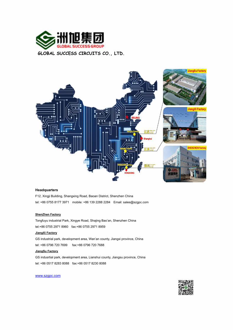
GLOBAL SUCCESS CIRCUITS CO., LTD. Headquarters F12, Xingji Building, Shangxing Road, Baoan District, Shenzhen China tel: +86 0755 8177 3971 mobile: +86 139 2288 2284 Email: [email protected] ShenZhen Factory Tongfuyu industrial Park, Xingye Road, Shajing Bao’an, Shenzhen China tel:+86 0755 2971 8960 fax:+86 0755 2971 8959 JiangXi Factory GS industrial park, development area, Wan’an county, Jiangxi province, China tel: +86 0796 720 7699 fax:+86 0796 720 7688 JiangSu Factory GS indusrtial park, development area, Lianshui county, Jiangsu province, China tel: +86 0517 8283 8088 fax:+86 0517 8230 8088 www.szgpc.com
-
Upload
angela-xia -
Category
Documents
-
view
28 -
download
3
Transcript of GSC catalogue
GLOBAL SUCCESS CIRCUITS CO., LTD.
HeadquartersF12, Xingji Building, Shangxing Road, Baoan District, Shenzhen China
tel: +86 0755 8177 3971 mobile: +86 139 2288 2284 Email: [email protected]
ShenZhen Factory
Tongfuyu industrial Park, Xingye Road, Shajing Bao’an, Shenzhen China
tel:+86 0755 2971 8960 fax:+86 0755 2971 8959
JiangXi Factory
GS industrial park, development area, Wan’an county, Jiangxi province, China
tel: +86 0796 720 7699 fax:+86 0796 720 7688
JiangSu Factory
GS indusrtial park, development area, Lianshui county, Jiangsu province, China
tel: +86 0517 8283 8088 fax:+86 0517 8230 8088
www.szgpc.com

Company Profile
Global Success Circuit Co.,Ltd. was
established in Shenzhen of China on May 2005,
which is a professional PCB manufacturer of
single side , double-layer, multilayer
board(2-20layers),high-precision pcb and
Aluminum- pcb With accurate market positioning,
customer-centric service concept and excellent
corporate culture. "Global Success Group" "with
three factories located in shenzhen,Jiangxi and
Jiangsu, and employs more than 1,000 people.
Shenzhen Global Success Circuits covers about 6000 square meters, with more than 150 people, mainly focus on sample
fabrication, small and medium quantity orders. Relying on our strong market and technical capacity, Shenzhen factory has very
mature quality control system on high-precision multilayer, buried-blind vias, impedance boards, high-frequency boards. For
quick-turn sample and small quantities board, we have very stable delivery and process capability which can assure 12-36 hours
of delivery to the users hand. The monthly production capacity up to 12,000 square meters.the business philosophies of fast
delivery, stable quality and excellent service, we have a good reputation in the various industries.
Jiangxi Global Success Circuits was founded in 2010. invests USD$10million to build a professionally big PCB enterprise
manufacturing double layer and multi-layer Glass plate PCB and Metal core PCB. Cover15,000 square meters. The new plant
completely purchasesadvanced automatic production equipments importing from developed countries. And also it employs
senior productive and administrative personnels and carries out ERP system efficiently controlling production process. It has
stable ability to deliver fast and guarantee best quality . Regarding important clients having orders of mass quantity of PCBs.
What's more, its capacity of manufacture PCB can reach 50,000 square meters and started production with orders oriented by
large and medium scaled quantity of PCBs from June, 2011.
Jiangsu Global Success Circuits was founded in 2014. The factory area is 25000 square meters. Using the newest,
automation , efficiency, technology and equipment .The capacity per moth is 50000 square meters .
Recent years, GSC ( Global Success Circuits) is developing quickly at 40% of growthrate per year continuously over the past
five years. All the products have wholly passed through the test of European Union "SGS-ROHS" and "SGS-REACH".What's more,
company has got ISO9001 Quality Management System Authentification, ULcertificate and ISO14001 nEnvironment
Management System Authentification, ISO/TS16949 Car Quality Management System Authentification And OHSAS18001
Occupation Health and Safety Management System certificate.
As the world's leading PCB manufacturer, "Global Success Group" has always adhere to the core Values of
customer-centric,marketorientation, sincere cooperation and commitment, Strive to provide high quality services to customers
around the world,. We not only effort to Achieve a win-win situation with customers and partners, but also actively fulfill social
Responsibility to be a practitioner of the time responsibility and spreaders of civilization as a corporate citizen.

Production Capacity
Items Specification
MaterialsFR4(High Tg150, 170, 180) , Aluminum base , Thick copper , FR2 , CEM3, Rogers,
PTFE
Finished Board
Thickness0.016" ~ 0.128" (0.4mm ~3.2mm)
Maximum Dimension 24" x 24" (610mm x 610mm) 30.5”X13” (1200mmX508mm)
Minimum Line Width
/ Spacing0.004" / 0.004" (0.1mm / 0.1mm)
Minimum Hole
Diameter0.010" (0.25mm)
Minimum Solder PAD
Diameter0.010" (0.25mm)
Hole Position
Precision0.003" (0.075mm)
Hole Spacing 0.012" (0.3mm)
Minimum Hole
Spacing0.02" (0.5mm)
Surface Treatmentlead-free HAL, Flash gold , immersion gold , immersion tin , immersion siliver , OSP,
gold finger plating, carbon ink printing, and peelable blue
Rough Plating of Wall <0.0012 (0.021mm)
Maximum Aspect
Ratio6.0 : 1
Minimum Ring 0.0045 (0.115mm)
Maximum Thickness
of WiringInner Layer: 2.5oz, Outer Layer:3.0oz
Minimum Spacing for
Weld Separation0.008 (0.2mm)
Minimum Width for
Weld Separation0.003 (0.075mm)
Minimum Height of
Characters0.032 (0.8mm)
Minimum Size of
Punched Hole0.1 (2.5mm)
Controlled Impedance +/- 10%
Outline Precision
(CNC)0.004mil (0.1mm)
Outline Precision
(Punch)0.002 mil (0.05mm)
HDI Construction BVH/ Build up/ 1+N+1/ 2+N+2

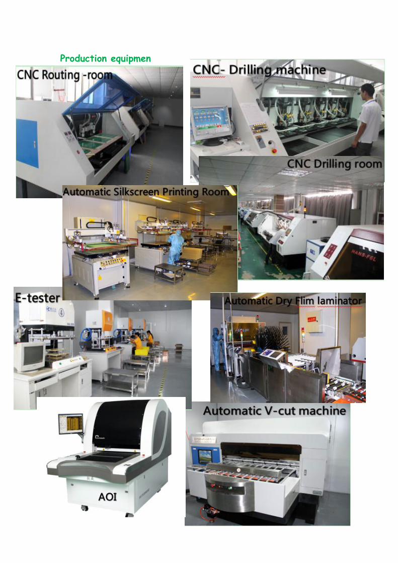
Production equipmen
Administrator
打字机文本
Administrator
打字机文本
Administrator
打字机文本
t
Administrator
打字机文本