GS2972 DS - mouser.com
126
1 of 125 GS2972 3G/HD/SD-SDI Serializer with Complete SMPTE Audio & Video Support Final Data Sheet Rev. 9 GENDOC-047479 September 2013 3G/HD/SD-SDI Serializer with Complete SMPTE Audio & Video Support GS2972 www.semtech.com Key Features • Operation at 2.970Gb/s, 2.970/1.001Gb/s, 1.485Gb/s, 1.485/1.001Gb/s and 270Mb/s • Supports SMPTE ST 425 (Level A and Level B), SMPTE ST 424, SMPTE ST 292, SMPTE ST 259-C and DVB-ASI • Integrated Cable Driver • Integrated, low-noise VCO • Integrated Narrow-Bandwidth PLL • Integrated Audio Embedder for up to 8 channels of 48kHz audio • Ancillary data insertion • Optional conversion from SMPTE ST 425 Level A to Level B for 1080p 50/60 4:2:2 10-bit • Parallel data bus selectable as either 20-bit or 10-bit • SMPTE video processing including TRS calculation and insertion, line number calculation and insertion, line based CRC calculation and insertion, illegal code re-mapping, SMPTE ST 352 payload identifier generation and insertion • GSPI host interface • +1.2V digital core power supply, +1.2V and +3.3V analog power supplies, and selectable +1.8V or +3.3V I/O power supply • -20ºC to +85ºC operating temperature range • Low power operation (typically at 400mW, including Cable Driver) • Small 11mm x 11mm 100-ball BGA package • Pb-free and RoHS compliant Applications Application: 1080p 50/60 Camera/Camcorder ADC Audio Processor Video Processor CCD 20-bit GS2972 3G-SDI HV F/PCLK CTRL/TIME CODE AES - IN AUDIO 1/2 AUDIO 3/4 Audio Clocks Storage: Tape/Disc /Solid State MIC OPTICS Application: Dual Link (HD-SDI) to Single Link (3G-SDI) Converter HD-SDI Deserializer (GS1559 or GS2970) Link A FIFO W R Deserializer Link B FIFO W R GS2972 GS4910 10-bit 3G-SDI HVF XTAL HV F/PCLK HV F/PCLK HV F/PCLK (GS1559 or GS2970) 10-bit 10-bit 10-bit HD-SDI HD-SDI HD-SDI EQ EQ GS2974B GS2974B Application: Multi-format Audio Embedder Module SD/HD/3G-SDI PCLK 10-bit GS2970 GS2972 ADC Switch Logic & Buffers SD/HD/3G-SDI Analog Audio Inputs AES Audio Inputs AUDIO 1/2 AUDIO 3/4 AUDIO 5/6 AUDIO 7/8 SRC GS4911 XTAL HVF Audio Clocks EQ GS2974B
Transcript of GS2972 DS - mouser.com

1 of 125
GS2972 3G/HD/SD-SDI Serializer with Complete SMPTE Audio & Video SupportFinal Data Sheet Rev. 9GENDOC-047479 September 2013
3G/HD/SD-SDI Serializer with Complete SMPTE Audio & Video Support
GS2972
www.semtech.com
Key Features• Operation at 2.970Gb/s, 2.970/1.001Gb/s, 1.485Gb/s,
1.485/1.001Gb/s and 270Mb/s
• Supports SMPTE ST 425 (Level A and Level B), SMPTE ST 424, SMPTE ST 292, SMPTE ST 259-C and DVB-ASI
• Integrated Cable Driver
• Integrated, low-noise VCO
• Integrated Narrow-Bandwidth PLL
• Integrated Audio Embedder for up to 8 channels of 48kHz audio
• Ancillary data insertion
• Optional conversion from SMPTE ST 425 Level A to Level B for 1080p 50/60 4:2:2 10-bit
• Parallel data bus selectable as either 20-bit or 10-bit
• SMPTE video processing including TRS calculation and insertion, line number calculation and insertion, line based CRC calculation and insertion, illegal code re-mapping, SMPTE ST 352 payload identifier generation and insertion
• GSPI host interface
• +1.2V digital core power supply, +1.2V and +3.3V analog power supplies, and selectable +1.8V or +3.3V I/O power supply
• -20ºC to +85ºC operating temperature range
• Low power operation (typically at 400mW, including Cable Driver)
• Small 11mm x 11mm 100-ball BGA package
• Pb-free and RoHS compliant
Applications
Application: 1080p 50/60 Camera/Camcorder
ADC AudioProcessor
VideoProcessor
CCD
20-bitGS2972
3G-SDI
HVF/PCLK
CTRL/TIMECODE
AES - INAUDIO 1/2
AUDIO 3/4Audio Clocks
Storage:Tape/Disc /Solid State
MIC
OPTICS
Application: Dual Link (HD-SDI) to Single Link (3G-SDI) Converter
HD-SDIDeserializer(GS1559 or
GS2970)
Link A
FIFO
W R
DeserializerLink B
FIFO
W R
GS2972
GS4910
10-bit
3G-SDI
HVF
XTAL
HVF/PCLK
HVF/PCLK
HVF/PCLK
(GS1559 orGS2970)
10-bit
10-bit
10-bit
HD-SDIHD-SDI
HD-SDI
EQ
EQ
GS2974B
GS2974B
Application: Multi-format Audio Embedder Module
SD/HD/3G-SDI
PCLK
10-bit
GS2970
GS2972
ADC
Switch Logic
&Buffers
SD/HD/3G-SDI
AnalogAudioInputs
AESAudioInputs
AUDIO 1/2
AUDIO 3/4
AUDIO 5/6
AUDIO 7/8
SRC
GS4911
XT
AL
HVF
Audio Clocks
EQGS2974B

2 of 125
GS2972 3G/HD/SD-SDI Serializer with Complete SMPTE Audio & Video SupportFinal Data Sheet Rev. 9GENDOC-047479 September 2013
www.semtech.com
DescriptionThe GS2972 is a complete SDI Transmitter, generating a SMPTE ST 424, SMPTE ST 292, SMPTE ST 259-C or DVB-ASI compliant serial digital output signal.
The integrated Narrow BW PLL allows the device to accept parallel clocks with high input jitter, and still provide a SMPTE compliant serial digital output.
The device can operate in four basic user selectable modes: SMPTE mode, DVB-ASI mode, Data-Through mode, or Standby mode.
In SMPTE mode, the GS2972 performs all SMPTE processing features. Both SMPTE ST 425 Level A and Level B formats are supported with optional conversion from Level A to Level B for 1080p 50/60 4:2:2 10-bit.
In DVB-ASI mode, the device will perform 8b/10b encoding prior to transmission.
In Data-Through mode, all SMPTE and DVB-ASI processing is disabled. The device can be used as a simple parallel to serial converter.
The device can also operate in a lower power Standby mode. In this mode, no signal is generated at the output.
The GS2972 integrates a fully SMPTE-compliant Cable Driver for SMPTE ST 259-C, SMPTE ST 292 and SMPTE ST 424 interfaces. It features automatic dual slew-rate selection, depending on 3Gb/s or HD or SD operational requirements.
In accordance with SMPTE ST 272 and SMPTE ST 299, up to eight channels (two audio groups) of serial digital audio may be embedded into the video data stream.The input audio signal formats supported by the device include AES/EBU, I2S and serial audio. 16, 20 and 24-bit audio formats are supported at 48kHz synchronous for SD modes and 48kHz synchronous or asynchronous in HD, 3Gb/s modes.
Application: Multi-format Digital VTR/Video Server
Storage:Tape/HDD/Solid State
AudioProcessor
VideoProcessor
20-bit
HVF/PCLK
Audio Inputs
V ideo Inputs
GS4911
Audio Clocks
GS2972 3G-SDI
SyncSeperator
AnalogSync
AUDIO 1/2
AUDIO 3/4
AUDIO 5/6
AUDIO 7/8
XTAL
KeyerKeyer
Application: Multi-format Presentation Switcher(Output Stage)
DVE Mixers Key & FillLogo
Inserter
Image Store
Key/Fill Inputs
GS297210-bit + Clk
20-bit + Clk
SD/HD/3G-SDIAuxiliary
Preview
Program
AudioMixer
AES from Input Demux
Voice-Over
Preset AES In
Program AES In Program AES Out
Preview AES Out
I2S Audio + Clocks
20-bit + Clk
GS4911
AnalogSync
XTAL
SyncSeperator
Clock &Sync Distribution
GS2972
GS2972
SD/HD/3G-SDI
SD/HD/3G-SDI
Application: 3Gb/s SDI Test Signal Generator
GS4911
AnalogSync
SyncSeperator
Video Signal
Generator
XTAL
AudioGenerator
Memory
HVF/PCLK
Audio Clocks
20-bit
GS2972
3G-SDI
AES 1/2
AES 3/4
AES 5/6
AES 7/8
HVF/PCLK

GS2972 3G/HD/SD-SDI Serializer with Complete SMPTE Audio & Video SupportFinal Data Sheet Rev. 9GENDOC-047479 September 2013
3 of 125
www.semtech.com
Functional Block Diagram
Figure A: GS2972 Functional Block Diagram
InputMux/
Demux
DIN[19:0]ANC DataInsertion
TRS , Line Number and CRC Insertion
EDHPacket
Insertion
DVB-ASI8b/10b
Encoder
F/DEV/VSYNCH/HSYNCTIM_861
Parallel to SerialConverter
MuxSMPTECableDriver
SDO
SDO
RSET
SDO_EN/DIS
PCLK
ACLK1ACLK2WCLK1WCLK2
Ain_1/2Ain_3/4Ain_5/6Ain_7/8
AUDIO_INTGRP1_EN/DISGRP2_EN/DIS
HANC/VANC
Blanking
PLL with Low NoiseVCO
Narrow BW PLL
LOCKED
DV
B_A
SI
NRZ/NRZISMPTE
Scrambler
LF VB
GR
ATE_SEL[1:0]
CD_VDD
CD_GND
CO
RE_
VD
D
CO
RE_
GN
D
IO_V
DD
IO_G
ND
RES
ET
STA
ND
BY
20BIT/10BIT
ANC_BLANK
PLL_VDD
PLL_GND
AVDD
AGND
VCO_VDD
VCO_GND
IOPR
OC
_EN
/DIS
SMPT
E_B
YPA
SS
SMPTE ST 425Level A to Level B
1080p 50/60 4:2:2 10-bit
SMPTE ST 352Generation and
Insertion
3G/HD/SDAudio
Embedding
GSPI HostInterface
CS_
TMS
SCLK
_TC
KSD
IN_T
DI
SDO
UT_
TDO
JTAGController
TMS
TDI
TDO
JTA
G/H
OST
TCK
Ded
icat
ed J
TAG
pin
s
Shar
ed J
TAG
an
d G
SPI p
ins
(fo
r d
rop
-in
co
mp
atib
ility
wit
h G
S157
2/82
)
GS2972 3G/HD/SD-SDI Serializer with Complete SMPTE Audio & Video SupportFinal Data Sheet Rev. 9GENDOC-047479 September 2013
4 of 125
www.semtech.com
Revision History
Version ECO PCN Date Changes and/or Modifications
9 014806 – September 2013 Updates throughout the document.
8 011355 – February 2013 Updated to the Semtech Template.
7 155820 56554 February 2011Added section 4.7.22.2 Blanking Values Following Audio Data Packet Insertion.
6 155608 – January 2011Clarified the function of the ACS_REGEN bit in Section 4.7.11 Audio Channel Status.
5 155080 56059 October 2010Revised power rating in standby mode. Documented CSUM behaviour in Section 4.8, Section 4.9.4 and Video Core Configuration and Status Registers.
4 153717 – March 2010
Updates throughout entire document. Added Figure 4-2, Figure 4-3 and Figure 4-4. Correction to registers 040h to 13Fh in Table 4-34: Video Core Configuration and Status Registers.
3 152220 – July 2009Updated Device Latency numbers in 2.4 AC Electrical Characteristics. Updates to 4.8 ANC Data Insertion. Replaced 7.3 Marking Diagram.
2 151320 − January 2009Correction to timing values in Table 4-1: GS2972 Digital Input AC Electrical Characteristics.
1 150803 − December 2008 Converted to Data Sheet. Updates to all sections.
0 150717 – October 2008 Converted to Preliminary Data Sheet.
D 149428 – August 2008Updated Typical Application Circuit. Applied new format to the document. Updates to all sections.
C 148810 – February 2008 Updates to all sections.
B 148770 – December 2007 Updates and revised 5.1 Typical Application Circuit.
A 147987 – December 2007 New Document.

GS2972 3G/HD/SD-SDI Serializer with Complete SMPTE Audio & Video SupportFinal Data Sheet Rev. 9GENDOC-047479 September 2013
5 of 125
www.semtech.com
Contents
Key Features ........................................................................................................................................................1
Applications.........................................................................................................................................................1
Description...........................................................................................................................................................2
Functional Block Diagram ..............................................................................................................................3
Revision History .................................................................................................................................................4
1. Pin Out............................................................................................................................................................ 10
1.1 Pin Assignment ............................................................................................................................... 10
1.2 Pin Descriptions ............................................................................................................................. 11
2. Electrical Characteristics ......................................................................................................................... 20
2.1 Absolute Maximum Ratings ....................................................................................................... 20
2.2 Recommended Operating Conditions .................................................................................... 20
2.3 DC Electrical Characteristics ..................................................................................................... 21
2.4 AC Electrical Characteristics ..................................................................................................... 23
3. Input/Output Circuits ............................................................................................................................... 26
4. Detailed Description.................................................................................................................................. 30
4.1 Functional Overview .................................................................................................................... 30
4.2 Parallel Data Inputs ....................................................................................................................... 31
4.2.1 Parallel Input in SMPTE Mode....................................................................................... 33
4.2.2 Parallel Input in DVB-ASI Mode................................................................................... 33
4.2.3 Parallel Input in Data-Through Mode......................................................................... 34
4.2.4 Parallel Input Clock (PCLK) ............................................................................................ 34
4.3 SMPTE Mode ................................................................................................................................... 35
4.3.1 H:V:F Timing ....................................................................................................................... 35
4.3.2 CEA 861 Timing.................................................................................................................. 38
4.4 DVB-ASI Mode ............................................................................................................................... 44
4.5 Data-Through Mode ..................................................................................................................... 44
4.6 Standby Mode ................................................................................................................................. 44
4.7 Audio Embedding .......................................................................................................................... 45
4.7.1 Serial Audio Data Inputs ................................................................................................. 45
4.7.2 Serial Audio Data Format Support............................................................................... 47
4.7.3 3G Mode................................................................................................................................ 49
4.7.4 HD Mode............................................................................................................................... 49
4.7.5 SD Mode................................................................................................................................ 50
4.7.6 Audio Embedding Operating Modes .......................................................................... 50
4.7.7 Audio Packet Detection................................................................................................... 51
4.7.8 Audio Packet Deletion ..................................................................................................... 51
4.7.9 Audio Packet Detection and Deletion ........................................................................ 51
4.7.10 Audio Mute (Default Off) .............................................................................................. 52
4.7.11 Audio Channel Status .................................................................................................... 53
4.7.12 Audio Crosspoint............................................................................................................. 54
4.7.13 Audio Word Clock .......................................................................................................... 55
4.7.14 Channel & Group Activation ....................................................................................... 55
4.7.15 Audio FIFO - SD............................................................................................................... 56
4.7.16 Audio FIFO - HD and 3G............................................................................................... 57

GS2972 3G/HD/SD-SDI Serializer with Complete SMPTE Audio & Video SupportFinal Data Sheet Rev. 9GENDOC-047479 September 2013
6 of 125
www.semtech.com
4.7.17 Five-frame Sequence Detection - SD........................................................................ 57
4.7.18 Frame Sequence Detection - HD/3G ........................................................................ 60
4.7.19 ECC Error Detection and Correction ........................................................................ 61
4.7.20 Audio Control Packet Insertion - SD......................................................................... 61
4.7.21 Audio Control Packet Insertion - HD and 3G......................................................... 62
4.7.22 Audio Data Packet Insertion........................................................................................ 63
4.7.23 Audio Interrupt Control ................................................................................................ 64
4.8 ANC Data Insertion ....................................................................................................................... 65
4.8.1 ANC Insertion Operating Modes .................................................................................. 65
4.8.2 3G ANC Insertion............................................................................................................... 67
4.8.3 HD ANC Insertion.............................................................................................................. 69
4.8.4 SD ANC Insertion............................................................................................................... 70
4.9 Additional Processing Functions .............................................................................................. 71
4.9.1 Video Format Detection .................................................................................................. 71
4.9.2 3G Format Detection ........................................................................................................ 74
4.9.3 ANC Data Blanking ........................................................................................................... 75
4.9.4 ANC Data Checksum Calculation and Insertion..................................................... 75
4.9.5 TRS Generation and Insertion ....................................................................................... 75
4.9.6 HD and 3G Line Number Calculation and Insertion.............................................. 76
4.9.7 Illegal Code Re-Mapping................................................................................................. 76
4.9.8 SMPTE ST 352 Payload Identifier Packet Insertion ................................................ 77
4.9.9 Line Based CRC Generation and Insertion (HD/3G) .............................................. 78
4.9.10 EDH Generation and Insertion ................................................................................... 78
4.9.11 GS2972 3G/HD HANC Space Considerations when Embedding Audio ...... 79
4.9.12 SMPTE ST 372 Conversion ........................................................................................... 79
4.9.13 Processing Feature Disable .......................................................................................... 80
4.10 SMPTE ST 352 Data Extraction ............................................................................................... 81
4.11 Serial Clock PLL ........................................................................................................................... 82
4.11.1 PLL Bandwidth................................................................................................................. 82
4.11.2 Lock Detect........................................................................................................................ 83
4.12 Serial Digital Output .................................................................................................................. 84
4.12.1 Output Signal Interface Levels ................................................................................... 85
4.12.2 Overshoot/Undershoot ................................................................................................. 85
4.12.3 Slew Rate Selection......................................................................................................... 86
4.12.4 Serial Digital Output Mute ........................................................................................... 86
4.13 GSPI Host Interface ..................................................................................................................... 87
4.13.1 Command Word Description ...................................................................................... 88
4.13.2 Data Read or Write Access........................................................................................... 88
4.13.3 GSPI Timing....................................................................................................................... 89
4.14 Host Interface Register Maps .................................................................................................. 91
4.14.1 Video Core Registers...................................................................................................... 91
4.14.2 SD Audio Core................................................................................................................ 100
4.14.3 HD and 3G Audio Core Registers............................................................................. 111
4.15 JTAG ID Codeword ................................................................................................................... 119
4.16 JTAG Test Operation ................................................................................................................ 119
4.17 Device Power-Up ...................................................................................................................... 119
4.18 Device Reset ................................................................................................................................ 119

GS2972 3G/HD/SD-SDI Serializer with Complete SMPTE Audio & Video SupportFinal Data Sheet Rev. 9GENDOC-047479 September 2013
7 of 125
www.semtech.com
5. Application Reference Design ............................................................................................................. 120
5.1 Typical Application Circuit ......................................................................................................120
6. References & Relevant Standards ....................................................................................................... 121
7. Package & Ordering Information ........................................................................................................ 122
7.1 Package Dimensions ................................................................................................................... 122
7.2 Packaging Data ............................................................................................................................. 123
7.3 Marking Diagram ......................................................................................................................... 123
7.4 Solder Reflow Profiles ................................................................................................................ 124
7.5 Ordering Information ................................................................................................................. 124
List of Figures
Figure 1-1: Pin Assignment ......................................................................................................................... 10Figure 3-1: Differential Output Stage (SDO/SDO) .............................................................................. 26Figure 3-2: Digital Input Pin ........................................................................................................................ 26Figure 3-3: Digital Input Pin with Schmitt Trigger (RESET) .............................................................. 26Figure 3-4: Digital Input Pin with weak pull-down - maximum pull-down current ............... 27Figure 3-5: Digital Input Pin with weak pull-up - maximum pull-up current ........................... 27Figure 3-6: Bidirectional Digital Input/Output Pin with programmable drive strength......... 27Figure 3-7: Bidirectional Digital Input/Output Pin with programmable drive strength......... 28Figure 3-8: VBG .............................................................................................................................................. 28Figure 3-9: Loop Filter .................................................................................................................................. 29Figure 4-1: GS2972 Video Host Interface Timing Diagrams ............................................................ 31Figure 4-2: H:V:F Output Timing - 3G Level A and HDTV 20-bit Mode ...................................... 36Figure 4-3: H:V:F Output Timing - 3G Level A and HDTV 10-bit Mode 3G Level B 20-bit Mode, each 10-bit stream ......................................................................................... 36Figure 4-4: H:V:F Output Timing - 3G Level B 10-bit Mode ............................................................. 36Figure 4-5: H:V:F Input Timing - HD 20-bit Input Mode ................................................................... 36Figure 4-6: H:V:F Input Timing - HD 10-bit Input Mode ................................................................... 37Figure 4-7: H:V:F Input Timing - SD 20-bit Mode ............................................................................... 37Figure 4-8: H:V:F Input Timing - SD 10-bit Mode ............................................................................... 37Figure 4-9: H:V:DE Input Timing 1280 x 720p @ 59.94/60 (Format 4) ........................................ 39Figure 4-10: H:V:DE Input Timing 1920 x 1080i @ 59.94/60 (Format 5) ..................................... 39Figure 4-11: H:V:DE Input Timing 720 (1440) x 480i @ 59.94/60 (Format 6&7) ....................... 40Figure 4-12: H:V:DE Input Timing 1280 x 720p @ 50 (Format 19) ................................................ 40Figure 4-13: H:V:DE Input Timing 1920 x 1080i @ 50 (Format 20) ............................................... 41Figure 4-14: H:V:DE Input Timing 720 (1440) x 576 @ 50 (Format 21&22) ................................ 41Figure 4-15: H:V:DE Input Timing 1920 x 1080p @ 59.94/60 (Format 16) ................................. 42Figure 4-16: H:V:DE Input Timing 1920 x 1080p @ 50 (Format 31) .............................................. 42Figure 4-17: H:V:DE Input Timing 1920 x 1080p @ 23.94/24 (Format 32) ................................. 42Figure 4-18: H:V:DE Input Timing 1920 x 1080p @ 25 (Format 33) .............................................. 43Figure 4-19: H:V:DE Input Timing 1920 x 1080p @ 29.97/30 (Format 34) ................................. 43Figure 4-20: ACLK to Data and Control Signal Input Timing .......................................................... 46Figure 4-21: I2S Audio Input Format ....................................................................................................... 47Figure 4-22: AES/EBU Audio Input Format .......................................................................................... 48Figure 4-23: Serial Audio, Left Justified, MSB First ............................................................................. 48Figure 4-24: Serial Audio, Left Justified, LSB First .............................................................................. 48Figure 4-25: Serial Audio, Right Justified, MSB First .......................................................................... 48Figure 4-26: Serial Audio, Right Justified, LSB First ........................................................................... 48Figure 4-27: Ancillary Data Packet Placement Example for SD Mode ........................................ 52Figure 4-28: ORL Matching Network, BNC and Coaxial Cable Connection ............................... 84

GS2972 3G/HD/SD-SDI Serializer with Complete SMPTE Audio & Video SupportFinal Data Sheet Rev. 9GENDOC-047479 September 2013
8 of 125
www.semtech.com
Figure 4-29: GSPI Application Interface Connection ........................................................................ 87Figure 4-30: Command Word Format ..................................................................................................... 88Figure 4-31: Data Word Format ................................................................................................................ 88Figure 4-32: Write Mode .............................................................................................................................. 89Figure 4-33: Read Mode ............................................................................................................................... 89Figure 4-34: GSPI Time Delay .................................................................................................................... 89Figure 4-35: Reset Pulse ............................................................................................................................. 119Figure 5-1: Typical Application Circuit ................................................................................................ 120Figure 7-1: Package Dimensions ............................................................................................................. 122Figure 7-2: Marking Diagram ................................................................................................................... 123Figure 7-3: Pb-free Solder Reflow Profile ............................................................................................ 124
List of Tables
Table 1-1: Pin Descriptions ......................................................................................................................... 11Table 2-1: Absolute Maximum Ratings................................................................................................... 20Table 2-2: Recommended Operating Conditions................................................................................ 20Table 2-3: DC Electrical Characteristics ................................................................................................. 21Table 2-4: AC Electrical Characteristics ................................................................................................. 23Table 4-1: GS2972 Digital Input AC Electrical Characteristics ....................................................... 31Table 4-2: GS2972 Input Video Data Format Selections................................................................... 31Table 4-3: GS2972 PCLK Input Rates....................................................................................................... 34Table 4-4: CEA861 Timing Formats ......................................................................................................... 38Table 4-5: Serial Audio Input Pin Description...................................................................................... 45Table 4-6: GS2972 Serial Audio Data Inputs - AC Electrical Characteristics............................. 46Table 4-7: Audio Input Formats ................................................................................................................ 47Table 4-8: GS2972 Audio Operating Mode Selection ........................................................................ 50Table 4-9: GS2972 SD Audio Crosspoint Channel Selection ........................................................... 54Table 4-10: Audio Source Host Interface Fields .................................................................................. 54Table 4-11: GS2972 SD Audio Buffer Size Selection .......................................................................... 56Table 4-12: GS2972 SD Audio Five Frame Sequence Sample Count............................................ 58Table 4-13: GS2972 SD Audio Group 1 Audio Sample Distribution - 525 line.......................... 58Table 4-14: GS2972 SD Audio Group 2 Audio Sample Distribution - 525 line.......................... 59Table 4-15: GS2972 SD Audio Group 3 Audio Sample Distribution - 525 line.......................... 59Table 4-16: GS2972 SD Audio Group 4 Audio Sample Distribution - 525 line.......................... 59Table 4-17: GS2972 SD Audio Group 1 Audio Sample Distribution - 625 line.......................... 59Table 4-18: GS2972 SD Audio Group 2 Audio Sample Distribution - 625 line.......................... 60Table 4-19: GS2972 SD Audio Group 3 Audio Sample Distribution - 625 line.......................... 60Table 4-20: GS2972 SD Audio Group 4 Audio Sample Distribution - 625 line.......................... 60Table 4-21: Audio Interrupt Control – Host Interface Bit Description ......................................... 64Table 4-22: Supported Video Standards................................................................................................. 72Table 4-23: IOPROC Register Bits ............................................................................................................. 80Table 4-24: SMPTE ST 352 Packet Data................................................................................................... 81Table 4-25: PCLK and Serial Digital Clock Rates ................................................................................. 82Table 4-26: GS2972 PLL Bandwidth......................................................................................................... 83Table 4-27: GS2972 Lock Detect Indication .......................................................................................... 83Table 4-28: Serial Digital Output - Serial Output Data Rate ............................................................ 84Table 4-29: RSET Resistor Value vs. Output Swing .............................................................................. 85Table 4-30: Serial Digital Output - Overshoot/Undershoot ............................................................. 85Table 4-31: Serial Digital Output - Rise/Fall Time............................................................................... 86Table 4-32: GSPI Time Delay...................................................................................................................... 89Table 4-33: GSPI AC Characteristics........................................................................................................ 90Table 4-34: Video Core Configuration and Status Registers............................................................ 91Table 4-35: SD Audio Core Configuration and Status Registers................................................... 100

GS2972 3G/HD/SD-SDI Serializer with Complete SMPTE Audio & Video SupportFinal Data Sheet Rev. 9GENDOC-047479 September 2013
9 of 125
www.semtech.com
Table 4-36: HD and 3G Audio Core Configuration and Status Registers .................................. 111Table 7-1: Packaging Data......................................................................................................................... 123Table 7-2: Ordering Information............................................................................................................. 124

GS2972 3G/HD/SD-SDI Serializer with Complete SMPTE Audio & Video SupportFinal Data Sheet Rev. 9GENDOC-047479 September 2013
10 of 125
www.semtech.com
1. Pin Out
1.1 Pin Assignment
Figure 1-1: Pin Assignment
1 32 4 5 6 7 8 9 10
A
B
C
D
E
F
G
H
J
K
VBG
DVB_ASI20bit/10bit
DIN18
SDO
LOCKED
ACLK1
JTAG/HOST
RESET
WCLK1
CORE_GND
SDO
DIN17
SDO_EN/DIS
F/DE H/HSYNC
VCO_GND
PLL_VDD
A_GND
DETECT_TRS
CORE_VDD
CORE_GND
CORE_GND
CORE_GND
VCO_VDD
CORE_VDD
CORE_VDD
STANDBY
RSV A_VDDLF
TDI
A_GND
RSV
IO_GND IO_VDD
CD_VDD
CD_GND
PLL_GND
PLL_GND
GRP2_EN/DIS
V/VSYNC
SDOUT_TDO
CS_TMS
SDIN_TDI
SCLK_TCK
SMPTE_BYPASS
IO_GNDIO_VDD
ANC_BLANK
AUDIO_INT
PCLK
AIN_1/2
AIN_3/4
AIN_5/6
AIN_7/8
TIM_861
TCK
IOPROC_EN/DIS
DIN15 DIN16 DIN19
DIN13 DIN14 DIN12
DIN11 DIN10
PLL_GND
DIN9 DIN8
DIN7 DIN6
DIN5 DIN4
DIN3
DIN1
DIN0DIN2
CORE_GND
CORE_GND
CORE_GND
CORE_VDD
CORE_GND
CD_GND
CD_GND
CD_GND
RSET
WCLK2
ACLK2
TDO
TMS
GRP1_EN/DIS
PLL_VDD
RSV RSV RSV RSV
RSV
RATE_SEL0
RATE_SEL1

GS2972 3G/HD/SD-SDI Serializer with Complete SMPTE Audio & Video SupportFinal Data Sheet Rev. 9GENDOC-047479 September 2013
11 of 125
www.semtech.com
1.2 Pin Descriptions
Table 1-1: Pin Descriptions
Pin Number
Name Timing Type Description
B3, A2, A1, B2, B1, C2, C1, C3, D1,
D2
DIN[19:10] Input
PARALLEL DATA BUS.
Please refer to the Input Logic parameters in the DC Electrical Characteristics table for logic level threshold and compatibility.
20-bit mode 20BIT/10BIT = HIGH
Data Stream 1/Luma data input in SMPTE mode (SMPTE_BYPASS = HIGH)
Data input in data through mode (SMPTE_BYPASS = LOW)
10-bit mode 20BIT/10BIT = LOW
Multiplexed Data Stream 1/Luma and Data Stream 2/Chroma data input in SMPTE mode (SMPTE_BYPASS = HIGH)
Data input in data through mode (SMPTE_BYPASS = LOW)
DVB-ASI data input in DVB-ASI mode (SMPTE_BYPASS = LOW) (DVB_ASI = HIGH)
A3 F/DE
Synch-ronous
withPCLK
Input
PARALLEL DATA TIMING.
Please refer to the Input Logic parameters in the DC Electrical Characteristics table for logic level threshold and compatibility.
TIM_861 = LOW: Used to indicate the ODD / EVEN field of the video signal when DETECT_TRS is set LOW. The device will set the F bit in all outgoing TRS signals for the entire period that the F input signal is HIGH (IOPROC_EN/DIS must also be HIGH). The F signal should be set HIGH for the entire period of field 2 and should be set LOW for all lines in field 1 and for all lines in progressive scan systems. The F signal is ignored when DETECT_TRS = HIGH.
TIM_861 = HIGH: The DE signal is used to indicate the active video period when DETECT_TRS is LOW. DE is HIGH for active data and LOW for blanking. See Section 4.3 and Section 4.3.2 for timing details. The DE signal is ignored when DETECT_TRS = HIGH.

GS2972 3G/HD/SD-SDI Serializer with Complete SMPTE Audio & Video SupportFinal Data Sheet Rev. 9GENDOC-047479 September 2013
12 of 125
www.semtech.com
A4 H/HSYNC
Synch-ronous
withPCLK
Input
PARALLEL DATA TIMING.
Please refer to the Input Logic parameters in the DC Electrical Characteristics table for logic level threshold and compatibility.
TIM_861 is LOW: The H signal is used to indicate the portion of the video line containing active video data, when DETECT_TRS is set LOW.
Active Line Blanking The H signal should be LOW for the active portion of the video line. The signal goes LOW at the first active pixel of the line, and then goes HIGH after the last active pixel of the line. The H signal should be set HIGH for the entire horizontal blanking period, including both EAV and SAV TRS words, and LOW otherwise.
TRS Based Blanking (H_CONFIG = 1h) The H signal should be set HIGH for the entire horizontal blanking period as indicated by the H bit in the received TRS ID words, and LOW otherwise.
TIM_861 = HIGH: The HSYNC signal indicates horizontal timing. See Section 4.3.
When DETECT_TRS is HIGH, this pin is ignored at all times. If DETECT_TRS is set HIGH and TIM_861 is set HIGH, the DETECT_TRS feature will take priority.
A5, E1, G10, K8
CORE_VDD Input PowerPower supply connection for digital core logic. Connect to +1.2V DC digital.
A6, B6 PLL_VDD Input Power Power supply pin for PLL. Connect to +1.2V DC analog.
A7 LFAnalog Output
Loop Filter component connection.
A8 VBG Output Bandgap voltage filter connection.
A9, D6, D7, D8, F4
RSV − These pins are reserved and should be left unconnected.
A10 A_VDD Input Power VDD for sensitive analog circuitry. Connect to +3.3VDC analog.
B4 PCLK Input
PARALLEL DATA BUS CLOCK.
Please refer to the Input Logic parameters in the DC Electrical Characteristics table for logic level threshold and compatibility.
3G 20-bit mode PCLK @ 148.5MHz
3G 10-bit mode DDR PCLK @ 148.5MHz
HD 20-bit mode PCLK @ 74.25MHz
HD 10-bit mode PCLK @ 148.5MHz
SD 20-bit mode PCLK @ 13.5MHz
SD 10-bit mode PCLK @ 27MHz
DVB-ASI mode PCLK @ 27MHz
B5, C5, E2, E5, E6, F5,
F6, G9CORE_GND Input Power GND connection for digital logic. Connect to digital GND.
Table 1-1: Pin Descriptions (Continued)
Pin Number
Name Timing Type Description

GS2972 3G/HD/SD-SDI Serializer with Complete SMPTE Audio & Video SupportFinal Data Sheet Rev. 9GENDOC-047479 September 2013
13 of 125
www.semtech.com
B7 VCO_VDD Input PowerPower pin for VCO. Connect to +1.2V DC analog followed by an RC filter (see Typical Application Circuit on page 120). VCO_VDD is nominally 0.7V.
B8 VCO_GND Input Power Ground connection for VCO. Connect to analog GND.
B9, B10 A_GND Input Power GND pins for sensitive analog circuitry. Connect to analog GND.
C4 V/VSYNC
Synch-ronous
withPCLK
Input
PARALLEL DATA TIMING.
Please refer to the Input Logic parameters in the DC Electrical Characteristics table for logic level threshold and compatibility.
TIM_861 = LOW:
The V signal is used to indicate the portion of the video field/frame that is used for vertical blanking, when DETECT_TRS is set LOW.
The V signal should be set HIGH for the entire vertical blanking period and should be set LOW for all lines outside of the vertical blanking interval.
The V signal is ignored when DETECT_TRS = HIGH.
TIM_861 = HIGH:
The VSYNC signal indicates vertical timing. See Section 4.3 for timing details.
The VSYNC signal is ignored when DETECT_TRS = HIGH.
C6, C7, C8 PLL_GND Input Power Ground connection for PLL. Connect to analog GND.
C9, D9, E9, F9
CD_GND Input PowerGround connection for the serial digital cable driver. Connect to analog GND.
C10, D10 SDO, SDO Output
Serial Data Output Signal.
Serial digital output signal operating at 2.97Gb/s, 2.97/1.001Gbs, 1.485Gb/s, 1.485 /1.001Gb/s or 270Mb/s.
The slew rate of the output is automatically controlled to meet SMPTE ST 424, SMPTE ST 292 and ST 259-C specifications according to the setting of the RATE_SEL0 and RATE_SEL1 pins.
D3 STANDBY InputPower Down input.
HIGH to power down device.
D4 SDO_EN/DIS Input
CONTROL SIGNAL INPUT.
Please refer to the Input Logic parameters in the DC Electrical Characteristics table for logic level threshold and compatibility.
Used to enable or disable the serial digital output stage.
When SDO_EN/DIS is LOW, the serial digital output signals SDO and SDO are disabled and become high impedance.
When SDO_EN/DIS is HIGH, the serial digital output signals SDO and SDO are enabled.
D5, F7 RSV − These pins are reserved and should be connected to CORE_GND.
Table 1-1: Pin Descriptions (Continued)
Pin Number
Name Timing Type Description

GS2972 3G/HD/SD-SDI Serializer with Complete SMPTE Audio & Video SupportFinal Data Sheet Rev. 9GENDOC-047479 September 2013
14 of 125
www.semtech.com
E3, E4RATE_SEL0,RATE_SEL1
Input
CONTROL SIGNAL INPUT.
Please refer to the Input Logic parameters in the DC Electrical Characteristics table for logic level threshold and compatibility.
Used to configure the operating data rate.
E7 TDI Input
COMMUNICATION SIGNAL INPUT.
Please refer to the Input Logic parameters in the DC Electrical Characteristics table for logic level threshold and compatibility.
Dedicated JTAG pin.
Test data in.
This pin is used to shift JTAG test data into the device when the JTAG/HOST pin is LOW.
E8 TMS Input
COMMUNICATION SIGNAL INPUT.
Please refer to the Input Logic parameters in the DC Electrical Characteristics table for logic level threshold and compatibility.
Dedicated JTAG pin.
Test mode start.
This pin is JTAG Test Mode Start, used to control the operation of the JTAG test when the JTAG/HOST pin is LOW.
E10 CD_VDD Input PowerPower for the serial digital cable driver. Connect to +3.3V DC analog.
F1, F2, H1, H2, J1, J2, K1, K2, J3,
K3
DIN[9:0] Input
PARALLEL DATA BUS.
Please refer to the Input Logic parameters in the DC Electrical Characteristics table for logic level threshold and compatibility.
In 10-bit mode, these pins are not used.
20-bit mode 20BIT/10BIT = HIGH
Data Stream 2/Chroma data input in SMPTE mode SMPTE_BYPASS = HIGH DVB_ASI = LOW
Data input in data through mode SMPTE_BYPASS = LOW DVB_ASI = LOW
Not Used in DVB-ASI mode SMPTE_BYPASS = LOW DVB_ASI = HIGH
10-bit mode 20BIT/10BIT = LOW
High impedance.
Table 1-1: Pin Descriptions (Continued)
Pin Number
Name Timing Type Description
RATE_SEL0 Data Rate
0
0
1
0
1
X
1.485 or 1.485/1.001Gb/s
2.97 or 2.97/1.001Gb/s
270Mb/s
RATE_SEL1

GS2972 3G/HD/SD-SDI Serializer with Complete SMPTE Audio & Video SupportFinal Data Sheet Rev. 9GENDOC-047479 September 2013
15 of 125
www.semtech.com
F3 DETECT_TRS Input
CONTROL SIGNAL INPUT.
Please refer to the Input Logic parameters in the DC Electrical Characteristics table for logic level threshold and compatibility.
Used to select external HVF timing mode or TRS extraction timing mode.
When DETECT_TRS is LOW, the device extracts all internal timing from the supplied H:V:F or CEA-861 timing signals, dependent on the status of the TIM861 pin.
When DETECT_TRS is HIGH, the device extracts all internal timing from TRS signals embedded in the supplied video stream.
F8 TDO Output
COMMUNICATION SIGNAL OUTPUT.
Please refer to the Output Logic parameters in the DC Electrical Characteristics table for logic level threshold and compatibility.
Dedicated JTAG pin.
JTAG Test Data Output.
This pin is used to shift results from the device when the JTAG/HOST pin is LOW.
F10 RSET InputAn external 1% resistor connected to this input is used to set the SDO/SDO output signal amplitude.
G1, H10 IO_VDD Input PowerPower connection for digital I/O. Connect to +3.3V or +1.8V DC digital.
G2, H9 IO_GND Input Power Ground connection for digital I/O. Connect to digital GND.
G3 TIM_861 Input
CONTROL SIGNAL INPUT.
Please refer to the Input Logic parameters in the DC Electrical Characteristics table for logic level threshold and compatibility.
Used to select external CEA-861 timing mode.
When DETECT_TRS is LOW and TIM-861 is LOW, the device extracts all internal timing from the supplied H:V:F timing signals.
When DETECT_TRS is LOW and TIM-861 is HIGH, the device extracts all internal timing from the supplied HSYNC, VSYNC, DE timing signals.
When DETECT_TRS is HIGH, the device extracts all internal timing from TRS signals embedded in the supplied video stream.
G4 20BIT/10BIT Input
CONTROL SIGNAL INPUT.
Please refer to the Input Logic parameters in the DC Electrical Characteristics table for logic level threshold and compatibility.
Used to select the input bus width.
G5 DVB_ASI Input
CONTROL SIGNAL INPUT.
Please refer to the Input Logic parameters in the DC Electrical Characteristics table for logic level threshold and compatibility.
Used to enable/disable the DVB-ASI data transmission.
When DVB_ASI is set HIGH and SMPTE_BYPASS is set LOW, then the device will carry out DVB-ASI word alignment, I/O processing and transmission.
When SMPTE_BYPASS and DVB_ASI are both set LOW, the device operates in data-through mode.
Table 1-1: Pin Descriptions (Continued)
Pin Number
Name Timing Type Description

GS2972 3G/HD/SD-SDI Serializer with Complete SMPTE Audio & Video SupportFinal Data Sheet Rev. 9GENDOC-047479 September 2013
16 of 125
www.semtech.com
G6 SMPTE_BYPASS Input
CONTROL SIGNAL INPUT.
Please refer to the Input Logic parameters in the DC Electrical Characteristics table for logic level threshold and compatibility.
Used to enable / disable all forms of encoding / decoding, scrambling and EDH insertion.
When set LOW, the device operates in data through mode (DVB_ASI= LOW), or in DVB-ASI mode (DVB_ASI = HIGH).
No SMPTE scrambling takes place and none of the I/O processing features of the device are available when SMPTE_BYPASS is set LOW.
When set HIGH, the device carries out SMPTE scrambling and I/O processing.
G7 IOPROC_EN/DIS Input
CONTROL SIGNAL INPUT.
Please refer to the Input Logic parameters in the DC Electrical Characteristics table for logic level threshold and compatibility.
Used to enable or disable the I/O processing features.
When IOPROC_EN/DIS is HIGH, the I/O processing features of the device are enabled. When IOPROC_EN/DIS is LOW, the I/O processing features of the device are disabled.
Only applicable in SMPTE mode.
G8 RESET Input
CONTROL SIGNAL INPUT.
Please refer to the Input Logic parameters in the DC Electrical Characteristics table for logic level threshold and compatibility.
Used to reset the internal operating conditions to default settings and to reset the JTAG sequence.
Normal mode (JTAG/HOST = LOW).
When LOW, all functional blocks will be set to default conditions and all input and output signals become high impedance.
When HIGH, normal operation of the device resumes.
JTAG test mode (JTAG/HOST = HIGH).
When LOW, all functional blocks will be set to default and the JTAG test sequence will be reset.
When HIGH, normal operation of the JTAG test sequence resumes.
H3 ANC_BLANK Input
CONTROL SIGNAL INPUT.
Please refer to the Input Logic parameters in the DC Electrical Characteristics table for logic level threshold and compatibility.
When ANC_BLANK is LOW, the Luma and Chroma input data is set to the appropriate blanking levels during the H and V blanking intervals.
When ANC_BLANK is HIGH, the Luma and Chroma data pass through the device unaltered.
Only applicable in SMPTE mode.
H4 LOCKED Output
STATUS SIGNAL OUTPUT.
Please refer to the Output Logic parameters in the DC Electrical Characteristics table for logic level threshold and compatibility.
PLL lock indication.
HIGH indicates PLL is locked.
LOW indicates PLL is not locked.
Table 1-1: Pin Descriptions (Continued)
Pin Number
Name Timing Type Description

GS2972 3G/HD/SD-SDI Serializer with Complete SMPTE Audio & Video SupportFinal Data Sheet Rev. 9GENDOC-047479 September 2013
17 of 125
www.semtech.com
H5 GRP2_EN/DIS InputEnables Audio Group 2 embedding. Set HIGH to enable.
Please refer to the Input Logic parameters in the DC Electrical Characteristics table for logic level threshold and compatibility.
H6 GRP1_EN/DIS InputEnables Audio Group 1 embedding. Set HIGH to enable.
Please refer to the Input Logic parameters in the DC Electrical Characteristics table for logic level threshold and compatibility.
H7 AUDIO_INT Output
STATUS SIGNAL OUTPUT.
Please refer to the Output Logic parameters in the DC Electrical Characteristics table for logic level threshold and compatibility.
Summary Interrupt from Audio Processing.
This signal is set HIGH by the device to indicate a problem with the audio processing which requires the Host processor to interrogate the interrupt status registers.
IO_VDD = +3.3V Drive Strength = 8mA
IO_VDD = +1.8V Drive Strength = 4mA
Note: By default, out of reset, the AUDIO_INT pin will output the HD_AUDIO_CLOCK, rather than the audio interrupt signal. In order to output the interrupt flags from the audio core as intended, the user must write 0001h to register 0232h.
H8 JTAG/HOST Input
CONTROL SIGNAL INPUT.
Please refer to the Input Logic parameters in the DC Electrical Characteristics table for logic level threshold and compatibility.
Used to select JTAG test mode or host interface mode.
When JTAG/HOST is HIGH, the host interface port is configured for JTAG test.
When JTAG/HOST is LOW, normal operation of the host interface port resumes and the separate JTAG pins become the JTAG port.
J4 AIN_5/6 InputSerial Audio Input; Channels 5 and 6.
Please refer to the Input Logic parameters in the DC Electrical Characteristics table for logic level threshold and compatibility.
J5 WCLK2 Input
48kHz Word Clock associated with AIN_5/6 and AIN_7/8 (channels 5, 6, 7 and 8).
Please refer to the Input Logic parameters in the DC Electrical Characteristics table for logic level threshold and compatibility.
J6 AIN_1/2 InputSerial Audio Input; Channels 1 and 2.
Please refer to the Input Logic parameters in the DC Electrical Characteristics table for logic level threshold and compatibility.
J7 WCLK1 Input
48kHz Word Clock associated with AIN_1/2 and AIN_3/4 (channels 1, 2, 3 and 4).
Please refer to the Input Logic parameters in the DC Electrical Characteristics table for logic level threshold and compatibility.
Table 1-1: Pin Descriptions (Continued)
Pin Number
Name Timing Type Description

GS2972 3G/HD/SD-SDI Serializer with Complete SMPTE Audio & Video SupportFinal Data Sheet Rev. 9GENDOC-047479 September 2013
18 of 125
www.semtech.com
J8 TCK Input
COMMUNICATION SIGNAL INPUT.
Please refer to the Input Logic parameters in the DC Electrical Characteristics table for logic level threshold and compatibility.
JTAG Serial Data Clock Signal.
This pin is the JTAG clock when the JTAG/HOST pin is LOW.
J9 SDOUT_TDO Output
COMMUNICATION SIGNAL OUTPUT.
Please refer to the Output Logic parameters in the DC Electrical Characteristics table for logic level threshold and compatibility.
Shared JTAG/HOST pin. Provided for compatibility with the GS1582. Serial Data Output/Test Data Output.
Host Mode (JTAG/HOST = LOW) This pin operates as the host interface serial output, used to read status and configuration information from the internal registers of the device.
JTAG Test Mode (JTAG/HOST = HIGH) This pin is used to shift test results and operates as the JTAG test data output, TDO (for new designs, use the dedicated JTAG port).
Note: If the host interface is not being used leave this pin unconnected.
IO_VDD = +3.3V Drive Strength = 12mA
IO_VDD = +1.8V Drive Strength = 4mA
J10 SCLK_TCK Input
COMMUNICATION SIGNAL INPUT.
Please refer to the Input Logic parameters in the DC Electrical Characteristics table for logic level threshold and compatibility.
Shared JTAG/HOST pin. Provided for pin compatibility with GS1582.
Serial data clock signal.
Host Mode (JTAG/HOST = LOW) SCLK_TCK operates as the host interface burst clock, SCLK. Command and data read/write words are clocked into the device synchronously with this clock.
JTAG Test Mode (JTAG/HOST = HIGH) This pin is the TEST MODE START pin, used to control the operation of the JTAG test clock, TCK (for new designs, use the dedicated JTAG port).
Note: If the host interface is not being used, tie this pin HIGH.
K4 AIN_7/8 Input Serial Audio Input; Channels 7 and 8.
K5 ACLK2 Input64 x WCLK associated with AIN_5/6 and AIN_7/8 (channels 5, 6, 7 and 8).
K6 AIN_3/4 Input Serial Audio Input; Channels 3 and 4.
K7 ACLK1 Input64 x WCLK associated with AIN_1/2 and AIN_3/4 (channels 1, 2, 3and 4).
Table 1-1: Pin Descriptions (Continued)
Pin Number
Name Timing Type Description
GS2972 3G/HD/SD-SDI Serializer with Complete SMPTE Audio & Video SupportFinal Data Sheet Rev. 9GENDOC-047479 September 2013
19 of 125
www.semtech.com
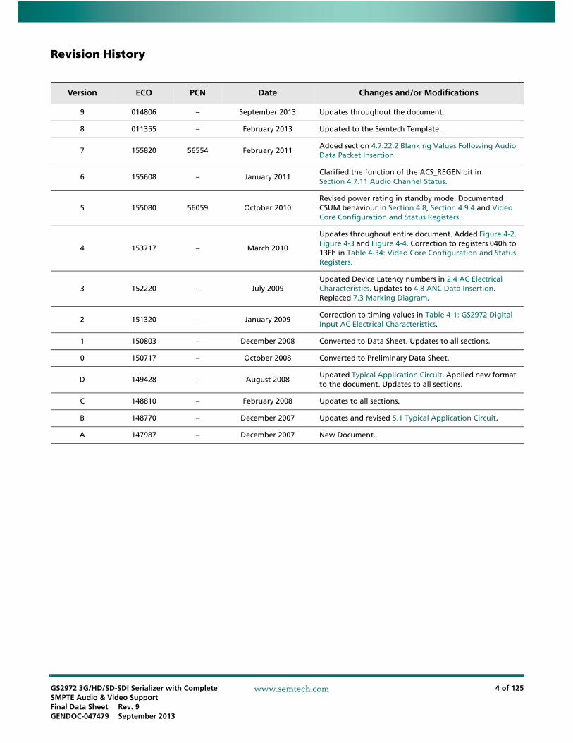
K9 CS_TMS Input
COMMUNICATION SIGNAL INPUT.
Please refer to the Input Logic parameters in the DC Electrical Characteristics table for logic level threshold and compatibility.
Chip select / test mode start.
JTAG Test mode (JTAG/HOST = HIGH) CS_TMS operates as the JTAG test mode start, TMS, used to control the operation of the JTAG test, and is active HIGH (for new designs, use the dedicated JTAG port).
Host mode (JTAG/HOST = LOW), CS_TMS operates as the host interface Chip Select, CS, and is active LOW.
K10 SDIN_TDI Input
COMMUNICATION SIGNAL INPUT.
Please refer to the Input Logic parameters in the DC Electrical Characteristics table for logic level threshold and compatibility.
Shared JTAG/HOST pin. Provided for pin compatibility with GS1582.
Serial data in/test data in.
In JTAG mode, this pin is used to shift test data into the device (for new designs, use the dedicated JTAG port).
In host interface mode, this pin is used to write address and configuration data words into the device.
Table 1-1: Pin Descriptions (Continued)
Pin Number
Name Timing Type Description
GS2972 3G/HD/SD-SDI Serializer with Complete SMPTE Audio & Video SupportFinal Data Sheet Rev. 9GENDOC-047479 September 2013
20 of 125
www.semtech.com
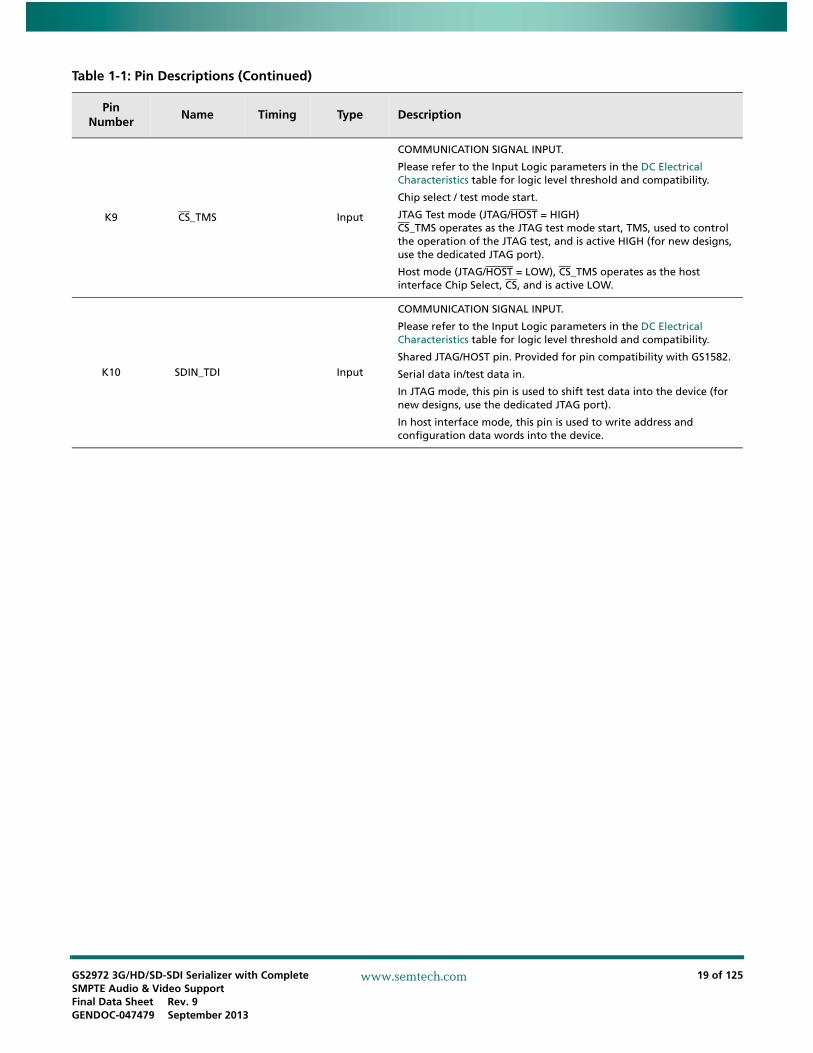
2. Electrical Characteristics
2.1 Absolute Maximum Ratings
2.2 Recommended Operating Conditions
Table 2-1: Absolute Maximum Ratings
Parameter Value/Units
Supply Voltage, Digital Core (CORE_VDD) -0.3V to +1.5V
Supply Voltage, Digital I/O (IO_VDD) -0.3V to +3.6V
Supply Voltage, Analog +1.2V (PLL_VDD, VCO_VDD) -0.3V to +1.5V
Supply Voltage, Analog +3.3V (CD_VDD, A_VDD) -0.3V to +3.6V
Input Voltage Range (RSET) -0.3V to (CD_VDD + 0.3)V
Input Voltage Range (VBG) -0.3V to (A_VDD + 0.3)V
Input Voltage Range (LF) -0.3V to (PLL_VDD + 0.3)V
Input Voltage Range (digital inputs) -2.0V to +5.25V
Temperature Range -40°C to +85°C
Storage Temperature Range -40°C to +125°C
Peak Reflow Temperature (JEDEC J-STD-020C) 260°C
ESD Sensitivity, HBM (JESD22-A114) 2kV
Note: Absolute Maximum Ratings are those values beyond which damage may occur. Functional operation outside of the ranges shown in Table 2-1 is not implied.
Table 2-2: Recommended Operating Conditions
Parameter Symbol Conditions Min Typ Max Units Note
Operating Temperature Range, Ambient
TA – -20 − 85 °C –
Supply Voltage, Digital Core CORE_VDD – 1.14 1.2 1.26 V –
Supply Voltage, Digital I/O IO_VDD+1.8V mode 1.71 1.8 1.89 V –
+3.3V mode 3.13 3.3 3.47 V –
Supply Voltage, PLL PLL_VDD – 1.14 1.2 1.26 V –
Supply Voltage, VCO VCO_VDD – − 0.7 − V 1
Supply Voltage, Analog A_VDD – 3.13 3.3 3.47 V –
Supply Voltage, CD CD_VDD – 3.13 3.3 3.47 V –

GS2972 3G/HD/SD-SDI Serializer with Complete SMPTE Audio & Video SupportFinal Data Sheet Rev. 9GENDOC-047479 September 2013
21 of 125
www.semtech.com
2.3 DC Electrical Characteristics
Operating Temperature Range – – -20 – 85 °C 2
Functional Temperature Range – – -40 – 85 °C 2
Notes:
1. This is 0.7V rather than 1.2V because there is a voltage drop across an external 105Ω resistor. See Typical Application Circuit.2. Operating Temperature Range guarantees the parameters given in the DC Electrical Characteristics and AC Electrical Characteristics.
Functional Temperature Range guarantees a device start-up.
Table 2-2: Recommended Operating Conditions (Continued)
Parameter Symbol Conditions Min Typ Max Units Note
Table 2-3: DC Electrical Characteristics
VCC = +3.3V ±5%, TA = -20°C to +85°C, unless otherwise shown
Parameter Symbol Conditions Min Typ Max Units Note
System
+1.2V Supply Current I1V2
10bit 3G − 135 200 mA −
20bit 3G − 135 200 mA −
10/20bit HD − 100 160 mA −
10/20bit SD − 75 120 mA −
DVB_ASI − 75 120 mA −
+1.8V Supply Current I1V8
10bit 3G − 15 30 mA −
20bit 3G − 15 32 mA −
10/20bit HD − 15 32 mA −
10/20bit SD − 3 10 mA −
DVB_ASI − 3 10 mA −
+3.3V Supply Current I3V3
10bit 3G − 90 110 mA −
20bit 3G − 90 110 mA −
10/20bit HD − 90 110 mA −
10/20bit SD − 70 90 mA −
DVB_ASI − 70 90 mA −
Total Device Power (IO_VDD = +1.8V)
P1D8
10bit 3G − 400 560 mW −
20bit 3G − 400 560 mW −
10/20bit HD − 350 510 mW −
10/20bit SD − 300 450 mW −
DVB_ASI − 300 450 mW −
Reset − 200 − mW −
Standby − 110 180 mW 1

GS2972 3G/HD/SD-SDI Serializer with Complete SMPTE Audio & Video SupportFinal Data Sheet Rev. 9GENDOC-047479 September 2013
22 of 125
www.semtech.com
Total Device Power (IO_VDD = +3.3V)
P3D3
10bit 3G − 430 600 mW −
20bit 3G − 450 610 mW −
10/20bit HD − 420 550 mW −
10/20bit SD − 320 450 mW −
DVB_ASI − 320 450 mW −
Reset − 230 − mW −
Standby − 110 180 mW 1
Digital I/O
Input Logic LOW VIL +3.3V or +1.8V operation IO_VSS-0.3 − 0.3 x IO_VDD
V −
Input Logic HIGH VIH +3.3V or +1.8V operation0.7 x
IO_VDD− IO_VDD+0.3 V −
Output Logic LOW VOLIOL=5mA, +1.8V operation − − 0.2 V −
IOL=8mA, +3.3V operation − − 0.4 V −
Output Logic HIGH VOHIOH=-5mA, +1.8V operation 1.4 − – V −
IOH=-8mA, +3.3V operation 2.4 − – V −
Serial Output
Serial Output Common Mode Voltage
VCMOUT75Ω load, RSET = 750Ω SD and HD mode
−CD_VDD -
VSDD/2− V −
Note:
1. Devices manufactured prior 1to April 1, 2011 consume 150mW of power in Standby mode.
Table 2-3: DC Electrical Characteristics (Continued)
VCC = +3.3V ±5%, TA = -20°C to +85°C, unless otherwise shown
Parameter Symbol Conditions Min Typ Max Units Note

GS2972 3G/HD/SD-SDI Serializer with Complete SMPTE Audio & Video SupportFinal Data Sheet Rev. 9GENDOC-047479 September 2013
23 of 125
www.semtech.com
2.4 AC Electrical Characteristics
Table 2-4: AC Electrical Characteristics
VCC = +3.3V ±5%, TA = -20°C to +85°C, unless otherwise shown
Parameter Symbol Conditions Min Typ Max Units Note
System
Device Latency
–3G bypass
(PCLK = 148.5 MHz)– 54 – PCLK –
–3G SMPTE without
audio (PCLK = 148.5 MHz)
– 95 – PCLK –
–3G SMPTE with
audio (PCLK = 148.5 MHz)
– 1106 – PCLK –
–
3G IOPROC disabled 20-bit
mode (PCLK = 148.5MHz)
– 94 – PCLK –
–HD bypass
(PCLK = 74.25 MHz)– 54 – PCLK –
–HD SMPTE without
audio (PCLK = 74.25 MHz)
– 95 – PCLK –
–HD SMPTE with
audio (PCLK = 74.25 MHz)
– 1106 – PCLK –
–
HD IOPROC disabled 10-bit
mode (PCLK = 74.25MHz)
98
–SD bypass
(PCLK = 27 MHz)– 54 – PCLK –
–SD SMPTE without
audio – 112 – PCLK –
–SD SMPTE with
audio– 638 – PCLK –
–
SD IOPROC disabled 10-bit
mode (PCLK = 27MHz)
– 94 – PCLK –
– DVB-ASI – 52 – PCLK –
Reset Pulse Width treset – 1 – – ms –
Parallel Input
Parallel Clock Frequency fPCLK – 13.5 – 148.5 MHz –
Parallel Clock Duty Cycle DCPCLK – 40 – 60 % –
Input Data Setup Time tsu 50% levels; +3.3V or +1.8V
operation
1.2 – – ns 1
Input Data Hold Time tih 0.8 – – ns 1
Serial Digital Output

GS2972 3G/HD/SD-SDI Serializer with Complete SMPTE Audio & Video SupportFinal Data Sheet Rev. 9GENDOC-047479 September 2013
24 of 125
www.semtech.com
Serial Output Data Rate DRSDO
– – 2.97 – Gb/s –
– – 2.97/1.001 – Gb/s –
– – 1.485 – Gb/s –
– – 1.485/1.001 – Gb/s –
– – 270 – Mb/s –
Serial Output Swing VSDDRSET = 750Ω
75Ω load 750 800 850 mVpp 2
Serial Output Rise/Fall Time 20% ~ 80%
trfSDO 3G/HD mode – 120 135 ps –
trfSDO SD mode 400 660 800 ps –
Mismatch in rise/fall time Δtr ,Δtf – – – 35 ps –
Duty Cycle Distortion – – – – 5 % 2
Overshoot– 3G/HD mode – 5 10 % 2
– SD mode – 3 8 % 2
Output Return Loss ORL
1.485GHz - 2.97GHz
– -12 – dB 3
5 MHz - 1.485 GHz – -18 – dB 3
Serial Output Intrinsic Jitter
tOJ
Pseudorandom and SMPTE Colour Bars
3G signal– 40 68 ps 4, 6
tOJ
Pseudorandom and SMPTE Colour Bars
HD signal– 50 95 ps 4, 6
Serial Output Intrinsic Jitter tOJ
Pseudorandom and SMPTE Colour Bars
SD signal– 200 400 ps 5
GSPI
GSPI Input Clock Frequency fSCLK
50% levels+3.3V or +1.8V
operation
– – 80 MHz –
GSPI Input Clock Duty Cycle DCSCLK 40 50 60 % –
GSPI Input Data Setup Time – 1.5 – – ns –
GSPI Input Data Hold Time – 1.5 – – ns –
GSPI Output Data Hold Time – 15pF load 1.5 – – ns –
CS low before SCLK rising edge
t0
50% levels+3.3V or +1.8V
operation1.5 – – ns –
Time between end of command word (or data in Auto-Increment mode) and the first SCLK of the following data word - write cycle
t4
50% levels+3.3V or +1.8V
operation
PCLK(MHz)
ns
– – ns –
unlocked 445
13.5 74.2
27.0 37.1
74.25 13.5
148.5 6.7
Table 2-4: AC Electrical Characteristics (Continued)
VCC = +3.3V ±5%, TA = -20°C to +85°C, unless otherwise shown
Parameter Symbol Conditions Min Typ Max Units Note
GS2972 3G/HD/SD-SDI Serializer with Complete SMPTE Audio & Video SupportFinal Data Sheet Rev. 9GENDOC-047479 September 2013
25 of 125
www.semtech.com
Time between end of command word (or data in Auto-Increment mode) and the first SCLK of the following data word - read cycle
t5
50% levels+3.3V or +1.8V
operation
PCLK(MHz)
ns
– – ns –
unlocked 1187
13.5 297
27.0 148.4
74.25 53.9
148.5 27
CS high after SCLK falling edge
t7
50% levels+3.3V or +1.8V
operation
PCLK(MHz)
ns
– – ns –
unlocked 445
13.5 74.2
27.0 37.1
74.25 13.5
148.5 6.7
Notes:
1. Input setup and hold time is dependent on the rise and fall time on the parallel input. Parallel clock and data with rise time or fall time greater than 500ps require larger setup and hold times.
2. Single Ended into 75Ω external load.3. ORL depends on board design.4. Alignment Jitter = measured from 100kHz to serial data rate/10.5. Alignment Jitter = measured from 1kHz to 27MHz.6. This is the maximum jitter for a BER of 10-12. The equivalent jitter value as per RP184 is 40ps max.
Table 2-4: AC Electrical Characteristics (Continued)
VCC = +3.3V ±5%, TA = -20°C to +85°C, unless otherwise shown
Parameter Symbol Conditions Min Typ Max Units Note

GS2972 3G/HD/SD-SDI Serializer with Complete SMPTE Audio & Video SupportFinal Data Sheet Rev. 9GENDOC-047479 September 2013
26 of 125
www.semtech.com
3. Input/Output Circuits
Figure 3-1: Differential Output Stage (SDO/SDO)
Figure 3-2: Digital Input Pin (20bit/10bit, ANC_BLANK, DETECT_TRS, DVB_ASI, RATE_SEL0, SMPTE_BYPASS, RATE_SEL1, TIM_861, F/DE, H/HSYNC, PCLK, V/VSYNC)
Figure 3-3: Digital Input Pin with Schmitt Trigger (RESET)
IREF
CD_VDD
SDO SDO
IO_VDD
200ΩInput Pin
IO_VDD
200ΩInput Pin
GS2972 3G/HD/SD-SDI Serializer with Complete SMPTE Audio & Video SupportFinal Data Sheet Rev. 9GENDOC-047479 September 2013
27 of 125
www.semtech.com
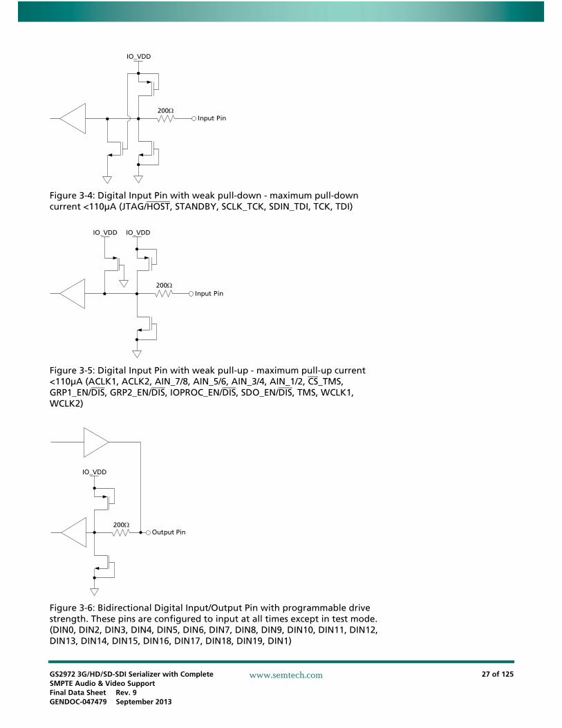
Figure 3-4: Digital Input Pin with weak pull-down - maximum pull-down current <110µA (JTAG/HOST, STANDBY, SCLK_TCK, SDIN_TDI, TCK, TDI)
Figure 3-5: Digital Input Pin with weak pull-up - maximum pull-up current <110µA (ACLK1, ACLK2, AIN_7/8, AIN_5/6, AIN_3/4, AIN_1/2, CS_TMS, GRP1_EN/DIS, GRP2_EN/DIS, IOPROC_EN/DIS, SDO_EN/DIS, TMS, WCLK1, WCLK2)
Figure 3-6: Bidirectional Digital Input/Output Pin with programmable drive strength. These pins are configured to input at all times except in test mode. (DIN0, DIN2, DIN3, DIN4, DIN5, DIN6, DIN7, DIN8, DIN9, DIN10, DIN11, DIN12, DIN13, DIN14, DIN15, DIN16, DIN17, DIN18, DIN19, DIN1)
IO_VDD
200ΩInput Pin
200ΩInput Pin
IO_VDD IO_VDD
IO_VDD
200ΩOutput Pin

GS2972 3G/HD/SD-SDI Serializer with Complete SMPTE Audio & Video SupportFinal Data Sheet Rev. 9GENDOC-047479 September 2013
28 of 125
www.semtech.com
Figure 3-7: Bidirectional Digital Input/Output Pin with programmable drive strength. These pins are configured to output at all times except in reset mode. (LOCKED, AUDIO_INT, SDOUT_TDO, TDO)
Figure 3-8: VBG
IO_VDD
200ΩOutput Pin
VBG50Ω
2kΩ
A_VDD

GS2972 3G/HD/SD-SDI Serializer with Complete SMPTE Audio & Video SupportFinal Data Sheet Rev. 9GENDOC-047479 September 2013
29 of 125
www.semtech.com
Figure 3-9: Loop Filter
30Ω
PLL_VDD
LF
30Ω

GS2972 3G/HD/SD-SDI Serializer with Complete SMPTE Audio & Video SupportFinal Data Sheet Rev. 9GENDOC-047479 September 2013
30 of 125
www.semtech.com
4. Detailed Description
4.1 Functional OverviewThe GS2972 is a Multi-Rate Transmitter with integrated SMPTE digital video processing and an integrated Cable Driver and embedded Audio Multiplexer. It provides a complete transmit solution at 2.970Gb/s, 2.970/1.001Gb/s, 1.485Gb/s, 1.485/1.001Gb/s or 270Mb/s.
The device has four basic modes of operation that must be set through external device pins: SMPTE mode, DVB-ASI mode, Data-Through mode and Standby mode.
In SMPTE mode, the device will accept 10-bit multiplexed or 20-bit demultiplexed SMPTE compliant data. By default, the device's additional processing features, including audio embedding, will be enabled in this mode.
In DVB-ASI mode, the GS2972 will accept an 8-bit parallel DVB-ASI compliant transport stream on DIN[17:10]. The serial output data stream will be 8b/10b encoded with stuffing characters added as per the standard.
Data-Through mode allows for the serializing of data not conforming to SMPTE or DVB-ASI streams. No additional processing will be done in this mode.
In addition, the device may be put into Standby, to reduce power consumption.
The serial digital output features a high-impedance mode and adjustable signal swing. The output slew rate is automatically set by the RATE_SEL0 and RATE_SEL1 pin setting.
The GS2972 provides several data processing functions; including generic ANC insertion, SMPTE ST 352 and EDH data packet generation and insertion, automatic video standards detection, and TRS, CRC, ANC data checksum, and line number calculation and insertion. These features are all enabled/disabled collectively using the external I/O processing pin, but may be individually disabled via internal registers accessible through the GSPI host interface.
Finally, the GS2972 contains a JTAG interface for boundary scan test implementations.

GS2972 3G/HD/SD-SDI Serializer with Complete SMPTE Audio & Video SupportFinal Data Sheet Rev. 9GENDOC-047479 September 2013
31 of 125
www.semtech.com
4.2 Parallel Data InputsData signal inputs enter the device on the rising edge of PCLK, as shown in Figure 4-1.
Figure 4-1: GS2972 Video Host Interface Timing Diagrams
DS1_0transition zone
DS2_0transition zone
PCLK
3.36ns
DS1_n-1DS1_n-1
transition zone DS2_0
TSU TH TH
DS1_0
DDR interfaceNote: DS = Data Stream as per SMPTE ST 425
DS2_* is launched on thenegative edge of PCLK
by the source chip to theGS2972
DS1_* is launched on thepositive edge of PCLK
by the source chip to theGS2972
TSU
data_1transition zone
data_1data_0transition zone
PCLK
PCLK period
DIN[19:0], F_DE,H_HSYNC, V_VSYNC
data_0
TH
SDR interface
DS* is launched on the positive edge of PCLKby the source chip to the GS2972
TSU THTSU
DIN[19:0], F_DE,H_HSYNC, V_VSYNC
TH
TH
Table 4-1: GS2972 Digital Input AC Electrical Characteristics
Parameter Symbol Conditions Min Typ Max Units
Input data set-up time tSU 50% levels; +1.8V operation
1.2 - - ns
Input data hold time tIH 0.8 - - ns
Input data set-up time tSU 50% levels; +3.3V operation
1.3 - - ns
Input data hold time tIH 0.8 - - ns
Table 4-2: GS2972 Input Video Data Format Selections
Input Data Format
Pin/Register Bit Settings
DIN[9:0] DIN[19:10]20BIT/10BIT
RATE_SEL0
RATE_SEL1
SMPTE_BYPASS
DVB_ASI
20-bit demultiplexed 3G format
HIGH LOW HIGH HIGH LOWData Stream
TwoData Stream One
20-bit data Input
3G formatHIGH LOW HIGH LOW LOW DATA DATA
20-bit demultiplexed HD format
HIGH LOW LOW HIGH LOW Chroma Luma

GS2972 3G/HD/SD-SDI Serializer with Complete SMPTE Audio & Video SupportFinal Data Sheet Rev. 9GENDOC-047479 September 2013
32 of 125
www.semtech.com
The GS2972 is a high performance 3Gb/s capable transmitter. In order to optimize the output jitter performance across all operating conditions, input levels and overshoot at the parallel video data inputs of the device need to be controlled. In order to do this, source series termination resistors should be used to match the impedance of the PCB data trace line. IBIS models can be used to simulate the board effects and then optimize the output drive strength and the termination resistors to allow for the best transition (one that produces minimal overshoot). If this is not viable, Semtech recommends matching the source series resistance to the trace impedance, and then adjusting the output drive strength to the minimum value that will give zero errors.
The above also applies to the PCLK input line. HVF and the Audio inputs should also be well terminated, however due to the lower data rates and transition density it is not as critical.
20-bit data Input
HD formatHIGH LOW LOW LOW LOW DATA DATA
20-bit demultiplexed SD format
HIGH HIGH X HIGH LOW Chroma Luma
20-bit data input
SD formatHIGH HIGH X LOW LOW DATA DATA
10-bit multiplexed
3G DDR formatLOW LOW HIGH HIGH LOW
High Impedance
Data Stream One/Data Stream
Two
10-bit multiplexed
HD formatLOW LOW LOW HIGH LOW
High Impedance
Luma/Chroma
10-bit data input
HD formatLOW LOW LOW LOW LOW
High Impedance
DATA
10-bit multiplexed
SD formatLOW HIGH X HIGH LOW
High Impedance
Luma/Chroma
10-bit multiplexed
SD formatLOW HIGH X LOW LOW
High Impedance
DATA
10-bit ASI input
SD formatLOW HIGH X LOW HIGH
High Impedance
DVB-ASI data
Table 4-2: GS2972 Input Video Data Format Selections (Continued)
Input Data Format
Pin/Register Bit Settings
DIN[9:0] DIN[19:10]20BIT/10BIT
RATE_SEL0
RATE_SEL1
SMPTE_BYPASS
DVB_ASI
GS2972 3G/HD/SD-SDI Serializer with Complete SMPTE Audio & Video SupportFinal Data Sheet Rev. 9GENDOC-047479 September 2013
33 of 125
www.semtech.com
4.2.1 Parallel Input in SMPTE Mode
When the device is operating in SMPTE mode (SMPTE_BYPASS = HIGH), data must be presented to the input bus in either multiplexed or demultiplexed form, depending on the setting of the 20BIT/10BIT pin.
When operating in 20-bit mode (20BIT/10BIT = HIGH), the input data format must be word aligned, demultiplexed Luma and Chroma data (SD or HD), or word aligned demultiplexed Data Stream One and Data Stream Two data (3G).
In 3G Level B mode, by default, the device takes Data Stream One input from data port DIN[19:10] and Data Stream Two input from DIN[9:0].
When operating in 10-bit mode (20BIT/10BIT = LOW), the input data format must be multiplexed Luma (Y) and Chroma (C) data (SD, HD), or multiplexed Data Stream One and Data Stream Two data (3G). C words precede Y words, and Data Stream 2 words precede Data Stream 1 words. In this mode, the data must be presented on the DIN[19:10] pins. The DIN[9:0] inputs are ignored.
In 3G 10-bit mode, the device operates in DDR mode. That is, the input data is sampled on both the rising and falling edges of the PCLK. In 3G mode, Data Stream Two words precede Data Stream One words. The Data Stream Two words are sampled on the rising edge of the input PCLK, and the Data Stream One words are sampled on the following falling edge. H, V and F timing pulses, if used, are sampled on the rising edge of PCLK.
4.2.1.1 Input Data Format in SDTI Mode
SDTI and HD-SDTI are a sub-set of SDI and HD-SDI formats. They may contain SDTI data on any line in the frame. Those lines which contain SDTI or HD-SDTI data are identified with an SDTI or HD-SDTI header packet in the HANC space.
The GS2972 does not differentiate between a signal carrying video and a signal carrying SDTI or HD-SDTI data in SD or HD formats. The user is responsible for ensuring that the headers and data are not corrupted.
4.2.2 Parallel Input in DVB-ASI Mode
The GS2972 is in DVB-ASI mode when the SMPTE_BYPASS pin is set LOW, the DVB_ASI pin is set HIGH, and the RATE_SEL0 pin is set HIGH. In this mode, all SMPTE processing features are disabled.
When operating in DVB-ASI mode, the device must be set to 10-bit mode by setting the 20BIT/10BIT pin LOW. The device will accept 8-bit data words on DIN[17:10], where DIN17 = HIN is the most significant bit of the encoded transport stream data and DIN10 = AIN is the least significant bit. In addition, DIN19 and DIN18 will be configured as the DVB-ASI control signals INSSYNCIN and KIN respectively.
DIN19 = INSSYNCIN DIN18 = KIN DIN17~10 = HIN ~ AIN where AIN is the least significant bit of the transport stream data.
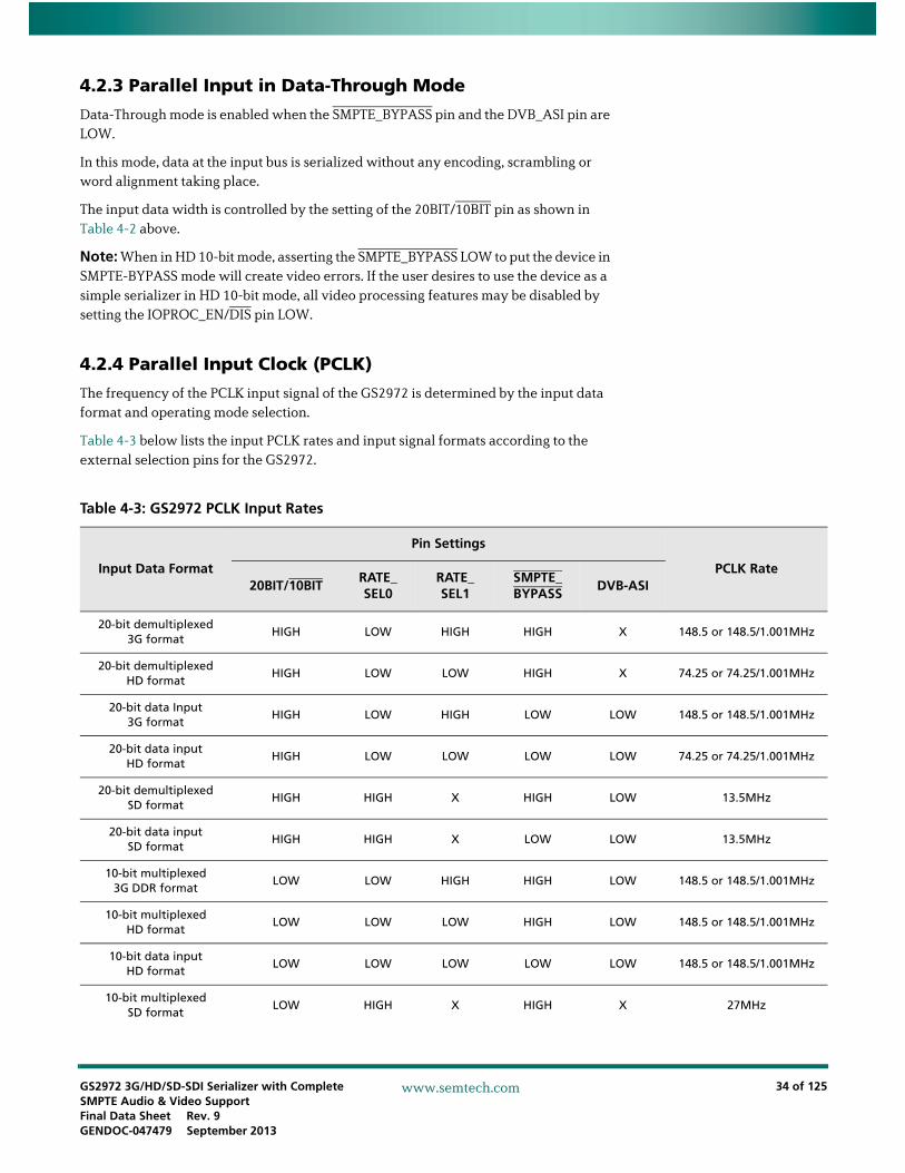
GS2972 3G/HD/SD-SDI Serializer with Complete SMPTE Audio & Video SupportFinal Data Sheet Rev. 9GENDOC-047479 September 2013
34 of 125
www.semtech.com
4.2.3 Parallel Input in Data-Through Mode
Data-Through mode is enabled when the SMPTE_BYPASS pin and the DVB_ASI pin are LOW.
In this mode, data at the input bus is serialized without any encoding, scrambling or word alignment taking place.
The input data width is controlled by the setting of the 20BIT/10BIT pin as shown in Table 4-2 above.
Note: When in HD 10-bit mode, asserting the SMPTE_BYPASS LOW to put the device in SMPTE-BYPASS mode will create video errors. If the user desires to use the device as a simple serializer in HD 10-bit mode, all video processing features may be disabled by setting the IOPROC_EN/DIS pin LOW.
4.2.4 Parallel Input Clock (PCLK)
The frequency of the PCLK input signal of the GS2972 is determined by the input data format and operating mode selection.
Table 4-3 below lists the input PCLK rates and input signal formats according to the external selection pins for the GS2972.
Table 4-3: GS2972 PCLK Input Rates
Input Data Format
Pin Settings
PCLK Rate20BIT/10BIT
RATE_SEL0
RATE_SEL1
SMPTE_BYPASS
DVB-ASI
20-bit demultiplexed3G format
HIGH LOW HIGH HIGH X 148.5 or 148.5/1.001MHz
20-bit demultiplexedHD format
HIGH LOW LOW HIGH X 74.25 or 74.25/1.001MHz
20-bit data Input3G format
HIGH LOW HIGH LOW LOW 148.5 or 148.5/1.001MHz
20-bit data input HD format
HIGH LOW LOW LOW LOW 74.25 or 74.25/1.001MHz
20-bit demultiplexed SD format
HIGH HIGH X HIGH LOW 13.5MHz
20-bit data input SD format
HIGH HIGH X LOW LOW 13.5MHz
10-bit multiplexed 3G DDR format
LOW LOW HIGH HIGH LOW 148.5 or 148.5/1.001MHz
10-bit multiplexed HD format
LOW LOW LOW HIGH LOW 148.5 or 148.5/1.001MHz
10-bit data input HD format
LOW LOW LOW LOW LOW 148.5 or 148.5/1.001MHz
10-bit multiplexed SD format
LOW HIGH X HIGH X 27MHz

GS2972 3G/HD/SD-SDI Serializer with Complete SMPTE Audio & Video SupportFinal Data Sheet Rev. 9GENDOC-047479 September 2013
35 of 125
www.semtech.com
4.3 SMPTE ModeThe function of this block is to carry out data scrambling according to SMPTE ST 424/SMPTE ST 292, and to carry out NRZ to NRZI encoding prior to presentation to the parallel to serial converter.
These functions are only enabled when the SMPTE_BYPASS pin is HIGH.
In addition, the GS2972 requires the DVB_ASI pin to be set LOW to enable this feature.
4.3.1 H:V:F Timing
In SMPTE mode, the GS2972 can automatically detect the video standard and generate all internal timing signals. The total line length, active line length, total number of lines per field/frame and total active lines per field/frame are calculated for the received parallel video.
When DETECT_TRS is LOW, the video standard and timing signals are based on the externally supplied H_Blanking, V_Blanking, and F_Digital signals. These signals are supplied by the H/HSYNC, V/VSYNC and F/DE pins respectively. When DETECT_TRS is HIGH, the video standard timing signals will be extracted from the embedded TRS ID words in the parallel input data. Both 8-bit and 10-bit TRS code words will be identified by the device.
Note: I/O processing must be enabled for the device to remap 8-bit TRS words to the corresponding 10-bit value for transmission.
The GS2972 determines the video standard by timing the horizontal and vertical reference information supplied at the H/HSYNC, V/VSYNC, and F/DE input pins, or contained in the TRS ID words of the received video data. Therefore, full synchronization to the received video standard requires at least one complete video frame.
Once synchronization has been achieved, the GS2972 will continue to monitor the received TRS timing or the supplied H, V, and F timing information to maintain synchronization. The GS2972 will lose all timing information immediately following loss of H, V and F.
The H signal timing should also be configured via the H_CONFIG bit of the internal IOPROC register as either active line based blanking or TRS based blanking.
Active line based blanking is enabled when the H_CONFIG bit is set LOW. In this mode, the H input should be HIGH for the entire horizontal blanking period, including the EAV and SAV TRS words. This is the default H timing used by the device.
10-bit data input SD format
LOW HIGH X LOW LOW 27MHz
10-bit ASI input SD format
LOW HIGH X LOW HIGH 27MHz
Table 4-3: GS2972 PCLK Input Rates (Continued)
Input Data Format
Pin Settings
PCLK Rate20BIT/10BIT
RATE_SEL0
RATE_SEL1
SMPTE_BYPASS
DVB-ASI
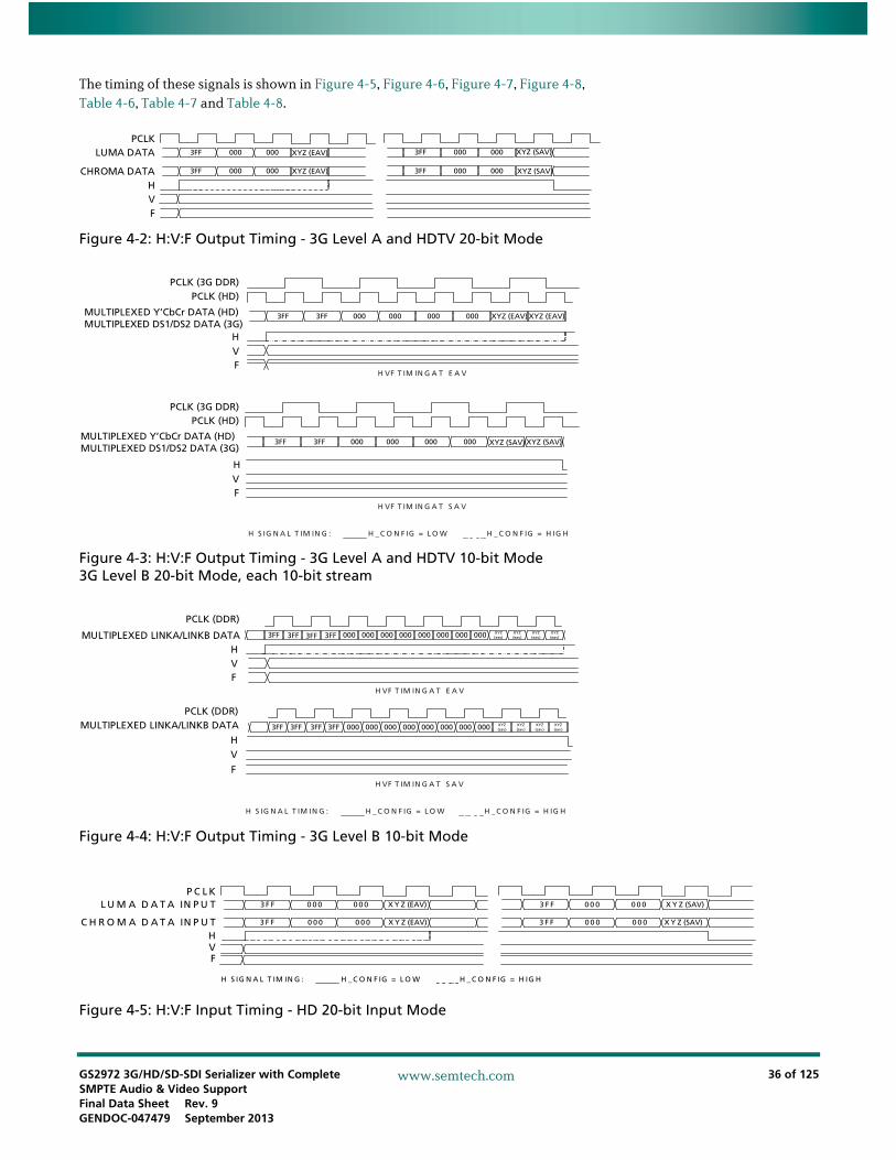
GS2972 3G/HD/SD-SDI Serializer with Complete SMPTE Audio & Video SupportFinal Data Sheet Rev. 9GENDOC-047479 September 2013
36 of 125
www.semtech.com
The timing of these signals is shown in Figure 4-5, Figure 4-6, Figure 4-7, Figure 4-8, Table 4-6, Table 4-7 and Table 4-8.
Figure 4-2: H:V:F Output Timing - 3G Level A and HDTV 20-bit Mode
Figure 4-3: H:V:F Output Timing - 3G Level A and HDTV 10-bit Mode 3G Level B 20-bit Mode, each 10-bit stream
Figure 4-4: H:V:F Output Timing - 3G Level B 10-bit Mode
Figure 4-5: H:V:F Input Timing - HD 20-bit Input Mode
PCLKLUMA DATA
CHROMA DATAH
0000003FF
0000003FF
VF
XYZ (SAV)0000003FF
0000003FF XYZ (SAV)XYZ (EAV)
XYZ (EAV)
0000003FF3FF 000000
PCLK (HD)
HVF
MULTIPLEXED Y’CbCr DATA (HD)MULTIPLEXED DS1/DS2 DATA (3G)
PCLK (3G DDR)
0000003FF3FF 000000 XYZ (EAV)MULTIPLEXED Y’CbCr DATA (HD)MULTIPLEXED DS1/DS2 DATA (3G)
HVF
PCLK (HD)PCLK (3G DDR)
H S IG N A L T IM IN G : H _ C O N F IG = L O W H _ C O N F IG = H IG H
H VF T IM IN G A T S A V
H VF T IM IN G A T E A V
XYZ (EAV)
XYZ (SAV)XYZ (SAV)
3FF
PCLK (DDR)
HV
F
MULTIPLEXED LINKA/LINKB DATA 3FF 3FF 3FF 000 000 000 000 000 000 000 000 XYZ(sav)
XYZ(sav)
XYZ(sav)
XYZ(sav)
MULTIPLEXED LINKA/LINKB DATA
PCLK (DDR)
HVF
3FF 000 000 000 000 000 000 000 000 XYZ(eav)
XYZ(eav)
XYZ(eav)
XYZ(eav)3FF 3FF 3FF
H S IG N A L T IM IN G : H _ C O N F IG = L O W H _ C O N F IG = H IG H
H VF T IM IN G A T E A V
H VF T IM IN G A T S A V
P C L KL U M A D A T A IN P U T
C H R O M A D A T A IN P U TH
X Y Z (EAV)0 0 00 0 03 F F
0 0 00 0 03 F F
VF
0 0 00 0 03 F F
0 0 00 0 03 F FX Y Z (EAV)
X Y Z (SAV)
X Y Z (SAV)
H S IG N A L T IM IN G : H _ C O N F IG = L O W H _ C O N F IG = H IG H

GS2972 3G/HD/SD-SDI Serializer with Complete SMPTE Audio & Video SupportFinal Data Sheet Rev. 9GENDOC-047479 September 2013
37 of 125
www.semtech.com
Figure 4-6: H:V:F Input Timing - HD 10-bit Input Mode
Figure 4-7: H:V:F Input Timing - SD 20-bit Mode
Figure 4-8: H:V:F Input Timing - SD 10-bit Mode
H V F T IM IN G A T S A V
0 0 00 0 03 F F3 F F 0 0 00 0 0P C L K
M U L T IP L E X E D Y 'C b C r D A T A IN P U T
HVF
H V F T IM IN G A T E A V
P C L K0 0 00 0 03 F F3 F F X Y Z (EAV)0 0 00 0 0M U L T IP L E X E D Y 'C b C r D A T A IN P U T
HVF
X Y Z (EAV)
X Y Z (SAV) X Y Z (SAV)
P C L KC H R O M A D A T A IN P U T
L U M A D A T A IN P U TH
0 0 03 F F
X Y Z (EAV)0 0 0
VF
0 0 03 F F
0 0 0
H S IG N A L T IM IN G : H _ C O N F IG = L O W H _ C O N F IG = H IG H
X Y Z (SAV)
M U L T IP L E X E D Y 'C b C r D A T A IN P U TP C L K
HVF
X Y Z (EAV)0 0 00 0 03 F F 0 0 00 0 03 F F X Y Z (SAV)
H S IG N A L T IM IN G : H _ C O N F IG = L O W H _ C O N F IG = H IG H

GS2972 3G/HD/SD-SDI Serializer with Complete SMPTE Audio & Video SupportFinal Data Sheet Rev. 9GENDOC-047479 September 2013
38 of 125
www.semtech.com
4.3.2 CEA 861 Timing
The GS2972 extracts timing information from externally provided HSYNC, VSYNC, and DE signals when CEA 861 timing mode is selected by setting DETECT_TRS = LOW and TIM_861 = HIGH.
Horizontal sync (H), Vertical sync (V), and Data Enable (DE) timing must be provided via the H/HSYNC, V/VSYNC and F/DE input pins. The host interface register bit H_CONFIG is ignored in CEA 861 input timing mode.
The GS2972 determines the EIA/CEA-861 standard and embeds EAV and SAV TRS words in the output serial video stream.
Video standard detection is not dependent on the HSYNC pulse width or the VSYNC pulse width and therefore the GS2972 tolerates non-standard pulse widths. In addition, the device can compensate for up to ±1 PCLK cycle of jitter on VSYNC with respect to HSYNC and sample VSYNC correctly.
Note 1: The period between the leading edge of the HSYNC pulse and the leading edge of Data Enable (DE) must follow the timing requirements described in the EIA/CEA-861 specification. The GS2972 embeds TRS words according to this timing relationship to maintain compatibility with the corresponding SMPTE standard.
Note 2: When CEA 861 standards 6 & 7 [720(1440)x480i] are presented to the GS2972, the device embeds TRS words corresponding to the timing defined in SMPTE ST 125 to maintain SMPTE compatibility.
CEA 861 standards 6 & 7 [720(1440)x480i] define the active area on lines 22 to 261 and 285 to 524 inclusive (240 active lines per field). SMPTE ST 125 defines the active area on lines 20 to 263 and 283 to 525 inclusive (244 lines on field 1, 243 lines on field 2).
Therefore, in the first field, the GS2972 adds two active lines above and two active lines below the original active image. In the second field, it adds two lines above and one line below the original active image.
The CEA861 Timing Formats are summarized in Table 4-4. and are shown in Figure 4-9 to Figure 4-19.
Table 4-4: CEA861 Timing Formats
Format Parameters
4 H:V:DE Input Timing 1280 x 720p @ 59.94/60Hz
5 H:V:DE Input Timing 1920 x 1080i @ 59.94/60Hz
6&7 H:V:DE Input Timing 720 (1440) x 480i @ 59.94/60Hz
19 H:V:DE Input Timing 1280 x 720p @ 50Hz
20 H:V:DE Input Timing 1920 x 1080i @ 50Hz
21&22 H:V:DE Input Timing 720 (1440) x 576 @ 50Hz
16 H:V:DE Input Timing 1920 x 1080p @ 59.94/60Hz
31 H:V:DE Input Timing 1920 x 1080p @ 50Hz
32 H:V:DE Input Timing 1920 x 1080p @ 23.94/24Hz
33 H:V:DE Input Timing 1920 x 1080p @ 25Hz
34 H:V:DE Input Timing 1920 x 1080p @ 29.97/30Hz

GS2972 3G/HD/SD-SDI Serializer with Complete SMPTE Audio & Video SupportFinal Data Sheet Rev. 9GENDOC-047479 September 2013
39 of 125
www.semtech.com
Figure 4-9: H:V:DE Input Timing 1280 x 720p @ 59.94/60 (Format 4)
Figure 4-10: H:V:DE Input Timing 1920 x 1080i @ 59.94/60 (Format 5)
1660 Total Horizontal Clocks per line
1280 Clocks for Active Video
DataEnable
220 clocks
40
370
110
HSYNC
Progressive Frame: 30 Vertical Blanking Lines 720 Active Vertical Lines
1650 clocks
DataEnable
HSYNC
110
VSYNC
260
745 746 747 748 749 750 1 2 3 4 5 6 7 25 26 745 746 750~ ~
~ ~
~ ~~ ~
~ ~~ ~
148 clocks
1920 Clocks for Active Video280
DataEnable
HSYNC
VSYNC
1123 1124 1125 1 2 3 4 5 6 7 8
DataEnable
HSYNC
2200 Total Horizontal Clocks per line
44
88
Field 1: 22 Vertical Blanking Lines
2200 clocks88
19 20 21 560 561 562
192
540 Active Vertical Lines per field
540 Active Vertical Lines per fieldField 2: 23 Vertical Blanking Lines
192882200 clocks
1100
VSYNC
DataEnable
HSYNC
560 561 562 563 564 565 566 567 568 569 570 582 583 584 1123 1124 1125
~~ ~
~ ~ ~
~ ~
~ ~~ ~
~ ~
~ ~

GS2972 3G/HD/SD-SDI Serializer with Complete SMPTE Audio & Video SupportFinal Data Sheet Rev. 9GENDOC-047479 September 2013
40 of 125
www.semtech.com
Figure 4-11: H:V:DE Input Timing 720 (1440) x 480i @ 59.94/60 (Format 6&7)
Figure 4-12: H:V:DE Input Timing 1280 x 720p @ 50 (Format 19)
1440 Clocks for Active Video276
DataEnable
1716 Total Horizontal Clocks per line
HSYNC
DataEnable
HSYNC
VSYNC
DataEnable
HSYNC
VSYNC
114 clocks124
38
Field 1: 22 Vertical Blanking Lines
1716 clocks 238
240 Active Vertical Lines per field
~~
~ ~
38
240 Active Vertical Lines per fieldField 2: 23 Vertical Blanking Lines
~ ~
524 525 1 2 3 4 5 6 7 8 9 21 22
~~
~ ~
23838 1716 clocks858
261 262 263 264 265 266 267 268 269 270 271 524 525 1284 285
261 262 263
220 clocks
1280 Clocks for Active Video700
DataEnable
HSYNC
VSYNC
745 746 747 748 749 750 1 2 3 4 5 6 7
DataEnable
HSYNC
1980 Total Horizontal Clocks per line
40
440
Progressive Frame: 30 Vertical Blanking Lines
1980 clocks440
745 746
260
720 Active Vertical Lines
~ ~~ ~
~ ~
~
25 26
~ ~~ ~
750

GS2972 3G/HD/SD-SDI Serializer with Complete SMPTE Audio & Video SupportFinal Data Sheet Rev. 9GENDOC-047479 September 2013
41 of 125
www.semtech.com
Figure 4-13: H:V:DE Input Timing 1920 x 1080i @ 50 (Format 20)
Figure 4-14: H:V:DE Input Timing 720 (1440) x 576 @ 50 (Format 21&22)
148 clocks
1920 Clocks for Active Video720
DataEnable
HSYNC
2640 Total Horizontal Clocks per line
44528
VSYNC
1123 1124 1125 1 2 3 4 5 6 7 8
DataEnable
HSYNC
Field 1: 22 Vertical Blanking Lines
2640 clocks528
19 20 21 560 561 562
192
540 Active Vertical Lines per field
540 Active Vertical Lines per fieldField 2: 23 Vertical Blanking Lines
1925282640 clocks
1320
VSYNC
DataEnable
HSYNC
560 561 562 563 564 565 566 567 568 569 570 582 583 584 1123 1124 1125
~~ ~
~ ~ ~
~ ~
~ ~~ ~
~ ~
~ ~
1440 Clocks for Active Video288
DataEnable
1728 Total Horizontal Clocks per line
HSYNC
138 clocks126
24
DataEnable
HSYNC
VSYNC
DataEnable
HSYNC
VSYNC
Field 1: 24 Vertical Blanking Lines
1728 clocks 264
288 Active Vertical Lines per field
~ ~
~ ~
24
288 Active Vertical Lines per fieldField 2: 25 Vertical Blanking Lines
~ ~
623 624 625 1 2 3 4 5 6 7 22 23
~~
~ ~
264241728 clocks
864
310 311 312 313 314 315 316 317 318 319 320 623 624 625335 336
310 311 312
~ ~

GS2972 3G/HD/SD-SDI Serializer with Complete SMPTE Audio & Video SupportFinal Data Sheet Rev. 9GENDOC-047479 September 2013
42 of 125
www.semtech.com
Figure 4-15: H:V:DE Input Timing 1920 x 1080p @ 59.94/60 (Format 16)
Figure 4-16: H:V:DE Input Timing 1920 x 1080p @ 50 (Format 31)
Figure 4-17: H:V:DE Input Timing 1920 x 1080p @ 23.94/24 (Format 32)
148 clocks
1920 Clocks for Active Video280
DataEnable
HSYNC
2200 Total Horizontal Clocks per line
44
88
VSYNC
1121 1122 1123 1124 1125 1 2 3 4 5 6 7
DataEnable
HSYNC
Progressive Frame: 45 Vertical Blanking Lines
2200 clocks88
1121 1122 1123 1124 1125
192
1080 Active Vertical Lines
~ ~~
~ ~
~
41 42
~ ~~
148 clocks
1920 Clocks for Active Video720
DataEnable
HSYNC
2640 Total Horizontal Clocks per line
44
528
VSYNC
1121 1122 1123 1124 1125 1 2 3 4 5 6 7
DataEnable
HSYNC
Progressive Frame: 45 Vertical Blanking Lines
2640 clocks528
1121 1122 1123 1124 1125
192
1080 Active Vertical Lines
~ ~~
~ ~
~
41 42
~ ~~
148 clocks
1920 Clocks for Active Video830
DataEnable
HSYNC
2750 Total Horizontal Clocks per line
44638
VSYNC
1121 1122 1123 1124 1125 1 2 3 4 5 6 7
DataEnable
HSYNC
Progressive Frame: 45 Vertical Blanking Lines
2750 clocks638
1121 1122 1123 1124 1125
192
1080 Active Vertical Lines
~ ~~
~ ~
~
41 42
~ ~~

GS2972 3G/HD/SD-SDI Serializer with Complete SMPTE Audio & Video SupportFinal Data Sheet Rev. 9GENDOC-047479 September 2013
43 of 125
www.semtech.com
Figure 4-18: H:V:DE Input Timing 1920 x 1080p @ 25 (Format 33)
Figure 4-19: H:V:DE Input Timing 1920 x 1080p @ 29.97/30 (Format 34)
148 clocks
1920 Clocks for Active Video720
DataEnable
HSYNC
2640 Total Horizontal Clocks per line
44
528
VSYNC
1121 1122 1123 1124 1125 1 2 3 4 5 6 7
DataEnable
HSYNC
Progressive Frame: 45 Vertical Blanking Lines
2640 clocks528
1121 1122 1123 1124 1125
192
1080 Active Vertical Lines
~ ~~
~ ~
~
41 42
~ ~~
148 clocks
1920 Clocks for Active Video280
DataEnable
HSYNC
2200 Total Horizontal Clocks per line
44
88
VSYNC
1121 1122 1123 1124 1125 1 2 3 4 5 6 7
DataEnable
HSYNC
Progressive Frame: 45 Vertical Blanking Lines
2220 clocks88
1121 1122 1123 1124 1125
192
1080 Active Vertical Lines
~ ~~
~ ~
~
41 42
~ ~~

GS2972 3G/HD/SD-SDI Serializer with Complete SMPTE Audio & Video SupportFinal Data Sheet Rev. 9GENDOC-047479 September 2013
44 of 125
www.semtech.com
4.4 DVB-ASI ModeWhen operating in DVB-ASI mode, all SMPTE processing features are disabled, and the device accepts 8-bit transport stream data and control signal inputs on the DIN[19:10] port.
This mode is only enabled when SMPTE_BYPASS pin is LOW, DVB_ASI pin is HIGH and the RATE_SEL0 pin is HIGH.
The interface consists of eight data bits and two control signals, INSSYNCIN and KIN.
When INSSYNCIN is set HIGH, the GS2972 inserts K28.5 sync characters into the data stream. This function is used to assist system implementations where the GS2972 may be preceded by a data FIFO.
The FIFO can be fed data at a rate somewhat less than 27MHz. The ‘FIFO empty’ signal could be used to feed the INSSYNCIN pin, causing the GS2972 to pad the data up to the transmission rate of 27MHz.
When KIN is set HIGH the data input is interpreted as a special character (such as a K28.5 sync character), as defined by the DVB-ASI standard. When KIN is set LOW the input is interpreted as data.
After sync signal insertion, the GS2972 8b/10b encodes the data, generating a 10-bit data stream for the parallel to serial conversion and transmission process.
4.5 Data-Through ModeThe GS2972 may be configured to operate as a simple parallel-to-serial converter. In this mode, the device passes data to the serial output without performing any scrambling or encoding.
Data-through mode is enabled only when both the SMPTE_BYPASS and DVB_ASI pins are set LOW.
4.6 Standby ModeThe STANDBY pin reduces power to a minimum by disabling all circuits except for the register configuration. Upon removal of the signal to the STANDBY pin, the device returns to its previous operating condition within 1 second, without requiring input from the host interface.
In addition, the serial digital output signals becomes high-impedance when the device is powered-down.

GS2972 3G/HD/SD-SDI Serializer with Complete SMPTE Audio & Video SupportFinal Data Sheet Rev. 9GENDOC-047479 September 2013
45 of 125
www.semtech.com
4.7 Audio EmbeddingThe GS2972 includes an Audio Multiplexer, which by default will be active when the Transmitter is configured for SMPTE mode.
Audio embedding is controlled by:
• GRP1_EN/DIS and GRP2_EN/DIS pins are set HIGH to enable embedding of their respective groups
• The AUDIO_INS bit in the IOPROC register is set LOW to enable audio embedding
• The IOPROC_EN/DIS pin is set HIGH to enable audio embedding
In non-SMPTE modes, the Audio Multiplexer will be powered down to reduce power.
Note: When audio is embedded by the GS2972, if either of the GRP1_EN/DIS or GRP2_EN/DIS pins are toggled, the output video stream is lost. For example: With a 3Gb/s SDI Level A input signal as the source, and either AES or I2S mode audio embedded; if one of the audio groups is disabled, there is no a longer valid video signal present at the output.
Toggling the audio disable pins on the fly must be avoided. The user has to set the pins before resetting the chip, and not change the setting during normal operation. The audio may be enabled or disabled during the operation of the chip by writing to the Host Interface registers. SD audio group embedding may be enabled, or disabled, by writing to ACT1...ACT8 bits of register 40Fh. HD/3G audio group embedding may be enabled, or disabled, by writing to ACT1...ACT8 bits of register 80Eh.
4.7.1 Serial Audio Data Inputs
The GS2972 supports the insertion of up to 8 channels of embedded audio, in two groups of 4 channels.
Each audio group has a dedicated audio group enable input pin; a Word Clock (WCLK) input pin operating at 48kHz; an Audio Clock input pin (ACLK) operating at 3.072MHz (64 x WCLK); and two serial digital audio input pins (AIN_1/2, etc.), supporting one stereo audio signal pair per pin.
The Serial Audio Data Inputs for each audio group are listed in Table 4-5.
Table 4-5: Serial Audio Input Pin Description
Pin Name Description
Audio Group 1
GRP1_EN/DIS Enable Input for Audio Group 1
AIN_1/2 Serial Audio Input; Channels 1 and 2
AIN_3/4 Serial Audio Input; Channels 3 and 4
ACLK164 x WCLK associated with AIN_1/2 and AIN_3/4 (channels 1, 2, 3and 4)
WCLK148kHz Word Clock associated with AIN_1/2 and AIN_3/4 (channels 1, 2, 3 and 4)
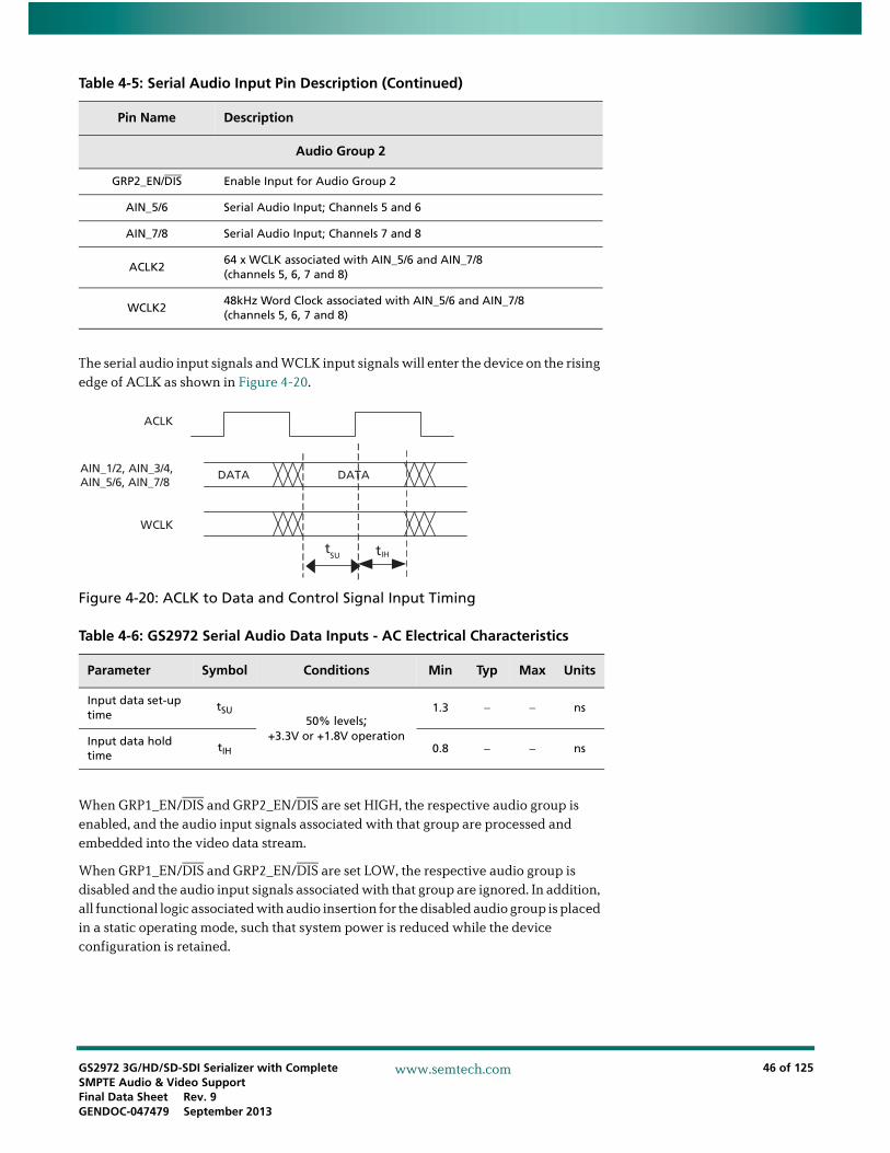
GS2972 3G/HD/SD-SDI Serializer with Complete SMPTE Audio & Video SupportFinal Data Sheet Rev. 9GENDOC-047479 September 2013
46 of 125
www.semtech.com
The serial audio input signals and WCLK input signals will enter the device on the rising edge of ACLK as shown in Figure 4-20.
Figure 4-20: ACLK to Data and Control Signal Input Timing
When GRP1_EN/DIS and GRP2_EN/DIS are set HIGH, the respective audio group is enabled, and the audio input signals associated with that group are processed and embedded into the video data stream.
When GRP1_EN/DIS and GRP2_EN/DIS are set LOW, the respective audio group is disabled and the audio input signals associated with that group are ignored. In addition, all functional logic associated with audio insertion for the disabled audio group is placed in a static operating mode, such that system power is reduced while the device configuration is retained.
Audio Group 2
GRP2_EN/DIS Enable Input for Audio Group 2
AIN_5/6 Serial Audio Input; Channels 5 and 6
AIN_7/8 Serial Audio Input; Channels 7 and 8
ACLK264 x WCLK associated with AIN_5/6 and AIN_7/8 (channels 5, 6, 7 and 8)
WCLK248kHz Word Clock associated with AIN_5/6 and AIN_7/8 (channels 5, 6, 7 and 8)
Table 4-6: GS2972 Serial Audio Data Inputs - AC Electrical Characteristics
Parameter Symbol Conditions Min Typ Max Units
Input data set-up time
tSU50% levels;
+3.3V or +1.8V operation
1.3 − − ns
Input data hold time
tIH 0.8 − − ns
Table 4-5: Serial Audio Input Pin Description (Continued)
Pin Name Description
ACLK
DATA DATAAIN_1/2, AIN_3/4,AIN_5/6, AIN_7/8
WCLK
tIHtSU

GS2972 3G/HD/SD-SDI Serializer with Complete SMPTE Audio & Video SupportFinal Data Sheet Rev. 9GENDOC-047479 September 2013
47 of 125
www.semtech.com
4.7.2 Serial Audio Data Format Support
The GS2972 supports the following serial audio data formats:
• I2S Audio (default)
• AES/EBU
• Serial Audio, Left Justified, MSB First
• Serial Audio, Left Justified, LSB First
• Serial Audio, Right Justified, MSB First
• Serial Audio, Right Justified, LSB First
By default (at power up or after system reset), the I2S data format is enabled.
The audio format can be different for both audio groups. Normally, AIN_1/2 and AIN_3/4 are embedded in Audio Group A, and AIN_5/6 and AIN_7/8 are embedded in Audio Group B. As well, the audio formats can be different within the same group.
Under normal conditions:
AMA sets the audio format for AIN_1/2 AMB sets the audio format for AIN_3/4 AMC sets the audio format for AIN_5/6 AMD sets the audio format for AIN_7/8
Note: These four formats can all be set to different modes if desired.
Table 4-7 shows the audio input formats for the GS2972. Note that the same values apply for AMB + LSB_FIRSTB, AMC + LSB_FIRSTC and AMD + LSB_FIRSTD.
Figure 4-21: I2S Audio Input Format
Table 4-7: Audio Input Formats
AMA[1:0](Address 40Bh for SD,
Address 80Ah for HD/3G)
LSB_FIRSTA(Address 40Fh for SD,
Address 80Eh for HD/3G)Audio Input Formats
00 X AES/EBU audio input
01 0 Serial audio input: Left Justified; MSB first
01 1 Serial audio input: Left Justified; LSB first
10 0 Serial audio input: Right Justified; MSB first
10 1 Serial audio input: Right Justified; LSB first
11 X 12S (default)
WCLK
ACLK
AIN[8/7:2/1]
MSB
032 12345622
LSB MSB
032 12345622
LSB
Channel A (Left) Channel B (Right)
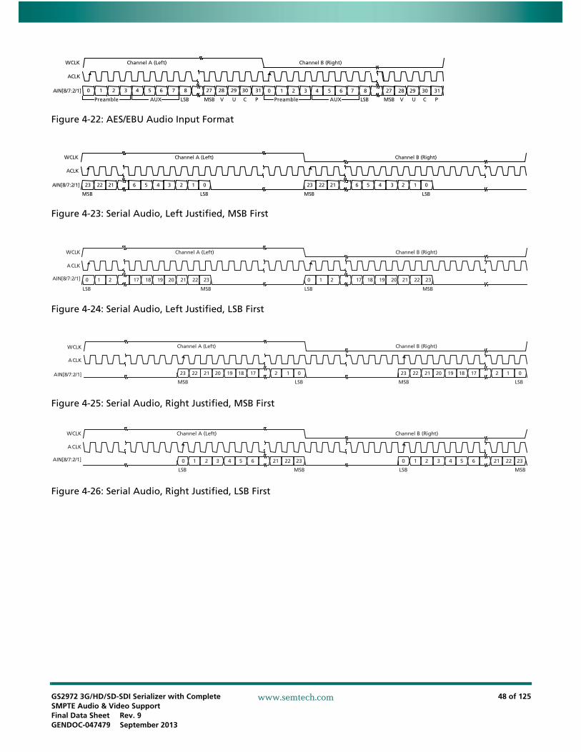
GS2972 3G/HD/SD-SDI Serializer with Complete SMPTE Audio & Video SupportFinal Data Sheet Rev. 9GENDOC-047479 September 2013
48 of 125
www.semtech.com
Figure 4-22: AES/EBU Audio Input Format
Figure 4-23: Serial Audio, Left Justified, MSB First
Figure 4-24: Serial Audio, Left Justified, LSB First
Figure 4-25: Serial Audio, Right Justified, MSB First
Figure 4-26: Serial Audio, Right Justified, LSB First
WCLK
ACLK
AIN[8/7:2/1] 1 2 3 4
LSB MSB
0
Channel A (Left) Channel B (Right)
5 6 7 8 27 2928 30 31 1 2 3 40 5 6 7 8 27 2928 30 31
AUXPreamble PCV U LSB MSBAUXPreamble PCV U
WCLK
ACLK
AIN[8/7:2/1] 23
MSB
022 12345621
LSB
23
MSB
022 12345621
LSB
Channel A (Left) Channel B (Right)
WCLK
ACLK
AIN[8/7:2/1] 0
LSB
321 2221201918172
MSB
0
LSB
321 2221201918172
MSB
Channel A (Left) Channel B (Right)
WCLK
ACLK
AIN[8/7:2/1] 23
MSB
022 1220 17181921
LSB
23
MSB
022 1220 17181921
LSB
Channel A (Left) Channel B (Right)
WCLK
ACLK
AIN[8/7:2/1] 0
LSB
321 22213 6542
MSB
0
LSB
321 22213 6542
MSB
Channel A (Left) Channel B (Right)

GS2972 3G/HD/SD-SDI Serializer with Complete SMPTE Audio & Video SupportFinal Data Sheet Rev. 9GENDOC-047479 September 2013
49 of 125
www.semtech.com
4.7.3 3G Mode
When the GS2972 is operating in 3G mode, 8 channels of audio in 4 pairs can be embedded in the serial output signal, according to SMPTE ST 299.
The 8 channels are in 2 groups, which are selectable via the host interface from the four groups allowed by SMPTE ST 299. The default is Group One and Group Two.
SMPTE ST 425 describes different mappings for the video signal, each with its own locations for audio data and control packets:
4.7.3.1 Level A Signals:
SMPTE ST 425 Level A describes a single video signal carried in a 3G bit stream.
The bit stream is made of two multiplexed virtual streams, Data Stream One and Data Stream Two.
Data Stream One carries audio control packets in the same way that the Y channel carries audio control packets in SMPTE ST 292 HD signals, but at twice the rate.
Data Stream Two carries audio data packets in the same way that the C channel carries audio data packets in SMPTE ST 292 HD signals, but at twice the rate.
For Level A signals with mappings 2 (1080i/p, 720p 4:4:4 10-bit), 3 (1080i/p 4:4:4 12-bit) or 4 (1080i/p, 720p 4:2:2 12-bit), the audio data packets are embedded at the full rate of 148.5MHz, but the clock phase bits are calculated assuming the original PCLK signal of 74.25MHz. This factor of two must be taken into consideration when calculating the clock bits.
SMPTE ST 425 requires SMPTE ST 352 payload packets to be embedded in both Data Stream One and Data Stream Two.
4.7.3.2 Level B Signals:
SMPTE ST 425 Level B describes the carriage of two SMPTE ST 292 signals in a single 3G bit stream. It also applies to a SMPTE ST 372 dual link signal.
The two signals are designated Link A and Link B. Each can carry audio data in the same way that a SMPTE ST 292 bit stream carries audio data.
The GS2972 is capable of embedding audio data onto either Link A or Link B of the Level B signal. The default will be Link A.
Link A and Link B are presented to the GS2972 as 10-bit signals at a 148.5MHz PCLK rate.
4.7.4 HD Mode
When the GS2972 is operating in HD mode, 8 channels of audio in 4 pairs are embedded in the serial output signal, according to SMPTE ST 299.
The 8 channels will be in 2 groups, which are selectable via the host interface from the 4 groups allowed by SMPTE ST 299. The default group is Group One and Group Two.

GS2972 3G/HD/SD-SDI Serializer with Complete SMPTE Audio & Video SupportFinal Data Sheet Rev. 9GENDOC-047479 September 2013
50 of 125
www.semtech.com
4.7.5 SD Mode
When the GS2972 is operating in SD mode, eight channels of audio in four pairs are embedded in the serial output signal, according to SMPTE ST 272. The eight channels will be in two groups, which are selectable via the host interface from the four groups allowed by SMPTE ST 272. The default group is Group One and Group Two.
4.7.6 Audio Embedding Operating Modes
Audio Embedding operates in one of three distinct modes:
1. Normal Mode (Default)
All previously embedded audio packets are deleted from the video stream. Arbitrary packets, SDTI packets and SMPTE ST 352 packets are not deleted. Up to two audio groups can be added to the video output. SDTI packets and SMPTE ST 352 packets are placed before the audio packets. Arbitrary packets are placed after the audio packets.
2. Cascade Mode
No previously embedded packets are deleted from the video stream. Up to two audio groups can be added to the video output. The added audio groups will not replace existing embedded audio groups. The added audio packets are appended to the last packet in the video input.
3. Group Replacement Mode
All packets associated with the groups being replaced are deleted. Up to two audio groups can be added to the video output. The added audio groups replace any embedded audio groups with the same group number. This will not affect any of the other audio groups, and they will remain in the data stream. The embedded audio groups are sorted in ascending order by audio group number. SDTI packets and SMPTE ST 352 packets are placed before the audio packets. Arbitrary packets are placed after the audio packets. The operating mode is selected using a combination of the EN_CASCADE and the AGR bits in the host interface, as stated in Table 4-8 below.
Table 4-8: GS2972 Audio Operating Mode Selection
Control Signals Operating Mode
EN_CASCADE=0, AGR=0 Normal Mode
EN_CASCADE=1, AGR=0 Cascade Mode
EN_CASCADE=0, AGR=1 Group Replacement Mode
EN_CASCADE=1, AGR=1 Group Replacement Mode

GS2972 3G/HD/SD-SDI Serializer with Complete SMPTE Audio & Video SupportFinal Data Sheet Rev. 9GENDOC-047479 September 2013
51 of 125
www.semtech.com
4.7.7 Audio Packet Detection
The input video stream to the GS2972 may already contain embedded audio packets.
The GS2972 detects these embedded packets, and signals their presence to the host interface. Register 404h is used for SD, register 803h is used for HD/3G.
4.7.8 Audio Packet Deletion
In Normal Mode (default), the GS2972 deletes all audio packets from the input video data stream.
In Cascade Mode, the GS2972 does not delete any audio packets from the input video data stream.
In Group Replacement Mode, the GS2972 does not delete any audio packets from the input video data stream.
In all operating modes, the GS2972 deletes all audio packets from the input video stream if any embedded audio packets do not fully comply with the SMPTE ST 291 standard.
4.7.9 Audio Packet Detection and Deletion
In SD modes, the first Ancillary Data Flag (ADF) must always be contiguous after the EAV words. For HD mode, the first ADF must always be contiguous after the two line CRC words.
Ancillary data packets with non-audio data ID words, such as arbitrary, EDH (SD only), SDTI header and SMPTE ST 352, are not deleted from the data stream. On lines where SMPTE ST 352 or SDTI header packets exist, the audio data packets must be contiguous from the ST 352 and SDTI packets. If this is not the case, all existing audio data and control packets will be deleted.
When CASCADE is set HIGH, all pre-existing audio data and control packets remain in the video stream.
When the AGR bit in the host interface is set HIGH, Audio Group Replacement mode is selected. In this mode, existing audio data and control packets are not deleted from the data stream.
In cases where the ADF is not placed immediately after the CRC or EAV words, or there are gaps between the packets, the audio core deletes all existing audio data and control packets, regardless of the CASCADE or AGR setting. Figure 4-27 shows an example of correct and incorrect placement of ancillary data packets for SD Mode.

GS2972 3G/HD/SD-SDI Serializer with Complete SMPTE Audio & Video SupportFinal Data Sheet Rev. 9GENDOC-047479 September 2013
52 of 125
www.semtech.com
Figure 4-27: Ancillary Data Packet Placement Example for SD Mode
4.7.10 Audio Mute (Default Off)
The GS2972 mutes all of the input channels when the MUTE_ALL host interface bit is set HIGH.
The GS2972 mutes any individual audio inputs as commanded by the following host interface fields:
MUTE1 - Mute input channel 1
MUTE2 - Mute input channel 2
MUTE3 - Mute input channel 3
MUTE4 - Mute input channel 4
MUTE5 - Mute input channel 5
MUTE6 - Mute input channel 6
MUTE7 - Mute input channel 7
MUTE8 - Mute input channel 8
BlankBlank Blank
EAV
HANC with space between EAV and Ancillary Data (Audio Packets will be deleted)
SAV
Au
dio
Gro
up
1
Au
dio
Gro
up
2
Correct placement of Ancillary Data within HANC Space
Blank
EAV
SAV
Au
dio
Gro
up
1
Au
dio
Gro
up
2
ST 3
52 /
SDTI
Pack
et
ST 3
52 /
SDTI
Pack
et

GS2972 3G/HD/SD-SDI Serializer with Complete SMPTE Audio & Video SupportFinal Data Sheet Rev. 9GENDOC-047479 September 2013
53 of 125
www.semtech.com
4.7.11 Audio Channel Status
The GS2972 adds audio channel status to those audio input channels that do not use the AES/EBU format.
The Audio Channel Status block complies with the AES3-1992 (ANSI S4.40-1992) standard.
The GS2972 uses the ACSR[183:0] host interface field as the source of audio channel status for those input channels that do not use the AES/EBU format.
The GS2972 replaces the Audio Channel Status block in all eight channels as commanded by the ACS_REGEN host interface bit. The status block information is supplied by the ACSR[183:0] host interface field.
The ACS_REGEN bit (SD core register 403h, HD/3G core register 802h) is set in two states:
ACS_REGEN = 0 -> Incoming Audio Channel Status is passed through the device to the output. For I2S audio formats, the transmitter will embed default audio channel status to the output stream.
ACS_REGEN = 1 -> Channel Status is based on user-defined data stored in the ACSR. With ACS_REGEN = 1, the GS2972 will serialize user-defined information to the output data. The user-defined data is applied to the output when the following steps are followed, and the time that the new status boundary occurs for the audio channel.
Audio channel status replacement follows the same procedure when replacing audio channel status for either AES or I2S audio formats.
To replace audio channel status, the following procedure should be used:
1. Write the desired ACS data to the ACSR [183:0] (SD Core registers 420h-42Ch, HD/3G Core registers 820h-82Ch).
2. Set ACS_REGEN bit = 1.
3. The Audio Channel Status on the serialized output will now contain the user defined ACS data.
To replace audio channel status on the fly, the following procedure should be used:
1. Write the desired ACS data to the ACSR [183:0] (SD Core registers 420h-42Ch, HD/3G Core registers 820h-82Ch)
2. Set ACS_REGEN bit = 1, if ACS_REGEN is already set, re-write ACS_REGEN = 1 again.
3. The Audio Channel Status on the serialized output will now contain the user-defined ACS data.
The GS2972 automatically calculates the CRC required for the Audio Channel Status block.
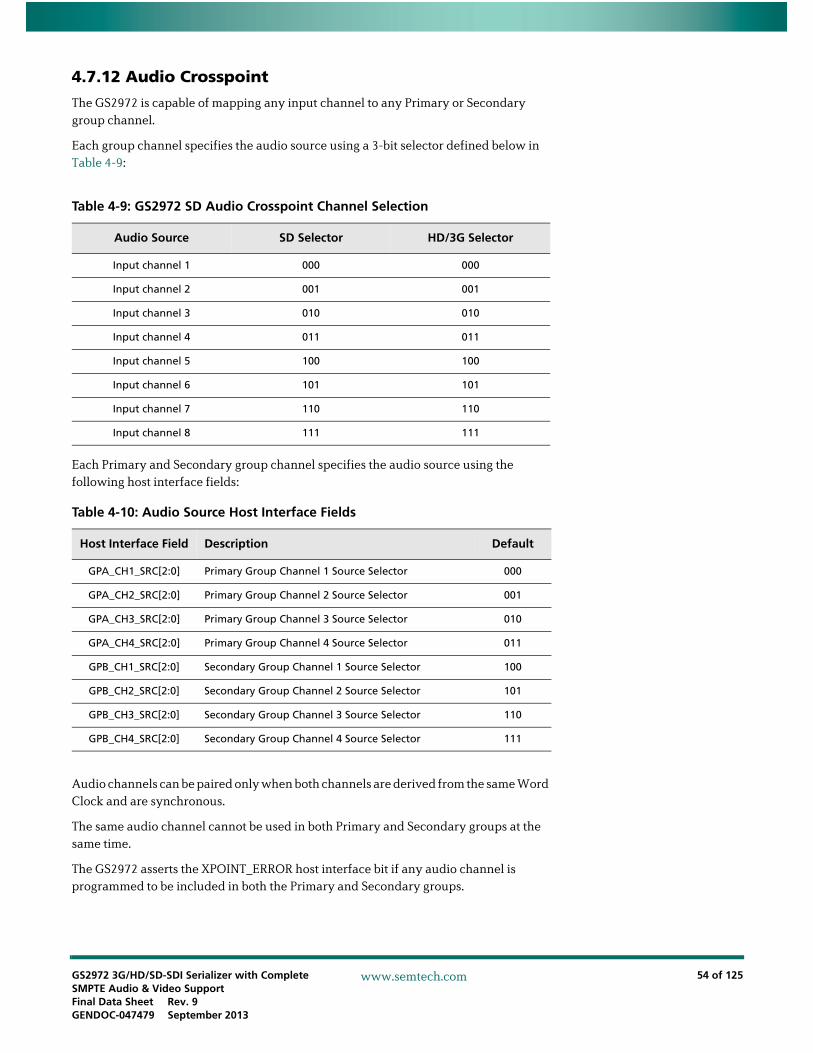
GS2972 3G/HD/SD-SDI Serializer with Complete SMPTE Audio & Video SupportFinal Data Sheet Rev. 9GENDOC-047479 September 2013
54 of 125
www.semtech.com
4.7.12 Audio Crosspoint
The GS2972 is capable of mapping any input channel to any Primary or Secondary group channel.
Each group channel specifies the audio source using a 3-bit selector defined below in Table 4-9:
Each Primary and Secondary group channel specifies the audio source using the following host interface fields:
Audio channels can be paired only when both channels are derived from the same Word Clock and are synchronous.
The same audio channel cannot be used in both Primary and Secondary groups at the same time.
The GS2972 asserts the XPOINT_ERROR host interface bit if any audio channel is programmed to be included in both the Primary and Secondary groups.
Table 4-9: GS2972 SD Audio Crosspoint Channel Selection
Audio Source SD Selector HD/3G Selector
Input channel 1 000 000
Input channel 2 001 001
Input channel 3 010 010
Input channel 4 011 011
Input channel 5 100 100
Input channel 6 101 101
Input channel 7 110 110
Input channel 8 111 111
Table 4-10: Audio Source Host Interface Fields
Host Interface Field Description Default
GPA_CH1_SRC[2:0] Primary Group Channel 1 Source Selector 000
GPA_CH2_SRC[2:0] Primary Group Channel 2 Source Selector 001
GPA_CH3_SRC[2:0] Primary Group Channel 3 Source Selector 010
GPA_CH4_SRC[2:0] Primary Group Channel 4 Source Selector 011
GPB_CH1_SRC[2:0] Secondary Group Channel 1 Source Selector 100
GPB_CH2_SRC[2:0] Secondary Group Channel 2 Source Selector 101
GPB_CH3_SRC[2:0] Secondary Group Channel 3 Source Selector 110
GPB_CH4_SRC[2:0] Secondary Group Channel 4 Source Selector 111

GS2972 3G/HD/SD-SDI Serializer with Complete SMPTE Audio & Video SupportFinal Data Sheet Rev. 9GENDOC-047479 September 2013
55 of 125
www.semtech.com
4.7.13 Audio Word Clock
When the GS2972 combines two stereo pair inputs into one audio group, the format allows for only one Word Clock, or sampling clock.
For the Primary group, the GS2972 uses the Word Clock associated with the source selected by the GPA_WCLK_SRC[2:0] host interface field. If in SD mode, address 40Ch. If in HD/3G mode, address 80Bh.
For the Secondary group, the GS2972 uses the Word Clock associated with the source selected by the GPB_WCLK_SRC[2:0] host interface field. If in SD mode, address 40Dh. If in HD/3G mode, address 80Ch.
For proper operation, the combined Stereo Pair inputs must have identical Word Clocks. WCLK is not required for AES/EBU audio.
4.7.14 Channel & Group Activation
The GS2972 embeds Primary group packets when any of the following host interface bits are set and the associated audio group enable pin is HIGH:
ACT1 Embed Primary group audio channel 1 ACT2 Embed Primary group audio channel 2 ACT3 Embed Primary group audio channel 3 ACT4 Embed Primary group audio channel 4
If none of the bits are set, then no audio will be embedded.
The GS2972 will embed Secondary group packets when any of the following host interface bits are set and the associated audio group enable pin is HIGH:
ACT5 Embed Secondary group audio channel 1 ACT6 Embed Secondary group audio channel 2 ACT7 Embed Secondary group audio channel 3 ACT8 Embed Secondary group audio channel 4
When an embedded packet contains one or more channels with the ACTx bit set to zero, the GS2972 replaces the data for those channels with null samples (all bits set to zero).
In the default state, the GS2972 embeds all audio channels in accordance with the setting of the respective audio group enable pins of the device.

GS2972 3G/HD/SD-SDI Serializer with Complete SMPTE Audio & Video SupportFinal Data Sheet Rev. 9GENDOC-047479 September 2013
56 of 125
www.semtech.com
4.7.15 Audio FIFO - SD
Each input channel has a First In First Out (FIFO) buffer that can hold up to 52 samples.
Samples are added (written) to the FIFO as they are received from the audio inputs.
Samples are removed (read) from the FIFO as they are embedded in audio data packets and audio extended packets.
After power up, reset or clear, the FIFO is in the start-up state where it will output zeroes until it has accumulated the start-up count of 26 samples.
When the start-up state ends, the buffer operates as a normal FIFO, and expects to receive an equal number of read and write operations over the period of five frames. At the end of five frames, the FIFO still has 26 samples in the buffer.
When the FIFO does not receive an equal number of read and write operations, the FIFO checks for the overflow and underflow conditions.
When a sample is required for embedding into a packet and the FIFO is holding less than 6 samples, the GS2972 prevents the underflow condition by repeating the last sample without removing a sample from the FIFO. Therefore, a sample will be duplicated.
When an input sample is received and the FIFO has room for less than six more samples, the GS2972 prevents the overflow condition by discarding the sample. Therefore, a sample will be dropped.
If 28 consecutive samples are duplicated or dropped, the audio FIFO is cleared and placed into the start-up state.
If the CLEAR_AUDIO host interface bit is set, the audio FIFO is cleared and put into the start-up state.
When the detected video standard changes, the audio FIFO is cleared and put into the start-up state.
The buffer size and start-up count can be reduced using the OS_SEL host interface field, as seen in Table 4-11 below:
Table 4-11: GS2972 SD Audio Buffer Size Selection
Address OS_SEL[1:0] Buffer Size Start-Up Count
00 52 samples (default) 26 samples
01 24 samples 12 samples
10 12 samples 6 samples
11 Reserved Reserved

GS2972 3G/HD/SD-SDI Serializer with Complete SMPTE Audio & Video SupportFinal Data Sheet Rev. 9GENDOC-047479 September 2013
57 of 125
www.semtech.com
4.7.16 Audio FIFO - HD and 3G
For HD and 3G formats, the audio FIFO block is a maximum of seven samples deep. According to SMPTE ST 299, audio samples are multiplexed immediately in the next HANC region after the audio sample occurs. A buffer size of seven samples takes into account that there are no samples after the switching line (for one line) and the worst-case video standard of 720p/24, plus a one-sample safety margin.
Due to the sample distribution used in HD video standards and the size of the buffer in HD mode, no checking is made for buffer underflow/overflow conditions. The pointers should maintain a variable offset between 0 and 6.
4.7.17 Five-frame Sequence Detection - SD
The GS2972 detects the frame sequence that describes the sample distribution for synchronous audio.
The frame sequence is used in the generation of audio control packets; where the Audio Frame Number (AFN) field describes the position of the current frame within the frame sequence.
The frame sequence is also used in the generation of Audio Sample Distribution for formats with 525 lines. Each frame has 1602 samples or 1601 samples, depending upon the frame sequence.
The GS2972 sets the AFN of the Primary group control packets to zero, unless the AFNA_AUTO host interface bit (400h bit 7) is set to produce automatic AFN generation.
The Multiplexer sets the AFN of the Secondary group control packets to zero unless the AFNB_AUTO host interface bit (800h bit 10) is set to produce automatic AFN generation.
When the frame rate is 25Hz, every frame has 1920 samples and the AFN is always set to one.
When the frame rate is 29.97Hz, an even number of samples (8008) are distributed over five frames in the following sequence:
1602 1601 1602 1601 1602
The GS2972 sets the AFN field to a number between one and five, depending on where the current frame lies within the sequence.
The GS2972 adds the offset specified in the AFN_OFS host interface field (400h bits 6-4) to the generated AFN. The result of the addition wraps around such that the AFN will always be in the range of one to five.
GS2972 3G/HD/SD-SDI Serializer with Complete SMPTE Audio & Video SupportFinal Data Sheet Rev. 9GENDOC-047479 September 2013
58 of 125
www.semtech.com
4.7.17.1 525-Line Audio Sample Distribution
As per the SMPTE ST 272 standard, the following sample distribution allows the embedding of 16 channels (4 audio groups) of 24-bit sampled audio into the HANC of 525-line based video formats.
The sample distribution is established for Group One and then offset by one line for each subsequent group. The sample distribution is as follows (start line is 12):
{[3](10+G),([4],[3]15)15,[4],[3](11-G),[0],[3](3+G),([4],[3]15)15,[4/3],[3]12,[4],[3](4-G),[0]}5
[#] = Number of samples / line [4/3] = One line with either 3 or 4 samples depending on five-frame sequence (#) = Number of times to repeat the sequence. When this # is 0, no samples are inserted G = Audio group number from 1 to 4 {…}5 = 5-frame sequence as shown in Table 4-12:
The following tables show the audio sample distribution for each of the four audio groups.
Each distribution has 525 lines.
Each distribution has 1602 samples or 1601 samples, based on the frame number in the five-frame sequence.
When 1602 samples are required in a frame, the [4/3] term represents a line with four samples.
When 1601 samples are required in a frame, the [4/3] term represents a line with three samples.
Table 4-12: GS2972 SD Audio Five Frame Sequence Sample Count
Frame Number of Samples
1 1602
2 1601
3 1602
4 1601
5 1602
Table 4-13: GS2972 SD Audio Group 1 Audio Sample Distribution - 525 line
[3](6),[4],[3](3) [0],[3](11) ([4],[3]15)15 [4],[3](10) [0],[3](4) ([4],[3]15)15 [4/3],[3](6)
Samples 31 33 735 34 12 735 22/21
Lines 10 12 240 11 5 240 7

GS2972 3G/HD/SD-SDI Serializer with Complete SMPTE Audio & Video SupportFinal Data Sheet Rev. 9GENDOC-047479 September 2013
59 of 125
www.semtech.com
4.7.17.2 625-Line Audio Sample Distribution
The GS2972 uses the following sample distribution to maximize the available space in the Ancillary Data region.
Note: the following formula starts from line 1:
[3]6,[0],[3](G-1),([4],[3]11)25,[4],[3](12-G),[0],[3](G-1),([4],[3]11)24,[4],[3](17-G)
• [#] represents one line with # samples
• (#) represents the number of times to repeat the line sequence
• [3](0) represents no lines and no samples
• G is the audio group number from one to four
The following tables show the audio sample distribution for each of the four audio groups:
Each distribution has 625 lines.
Each distribution has 1920 samples.
Table 4-14: GS2972 SD Audio Group 2 Audio Sample Distribution - 525 line
[3](7),[4],[3](2) [0],[3](12) ([4],[3]15)15 [4],[3](9) [0],[3](5) ([4],[3]15)15 [4/3],[3](5)
Samples 31 36 735 31 15 735 19/18
Lines 10 13 240 10 6 240 6
Table 4-15: GS2972 SD Audio Group 3 Audio Sample Distribution - 525 line
[3](8),[4],[3](1) [0],[3](13) ([4],[3]15)15 [4],[3](8) [0],[3](6) ([4],[3]15)15 [4/3],[3](4)
Samples 31 39 735 28 21 735 16/15
Lines 10 14 240 9 7 240 5
Table 4-16: GS2972 SD Audio Group 4 Audio Sample Distribution - 525 line
[3](9),[4],[3](0) [0],[3](14) ([4],[3]15)15 [4],[3](7) [0],[3](7) ([4],[3]15)15 [4/3],[3](3)
Samples 31 42 735 25 21 735 13/12
Lines 10 15 240 8 8 240 4
Table 4-17: GS2972 SD Audio Group 1 Audio Sample Distribution - 625 line
[3]6 [0],[3](0) ([4],[3]11)25 [4],[3](11) [0],[3](0) ([4],[3]11)24 [4],[3](16)
Samples 18 0 925 37 0 888 52
Lines 6 1 300 12 1 288 17

GS2972 3G/HD/SD-SDI Serializer with Complete SMPTE Audio & Video SupportFinal Data Sheet Rev. 9GENDOC-047479 September 2013
60 of 125
www.semtech.com
4.7.18 Frame Sequence Detection - HD/3G
The GS2972 detects the frame sequence that describes the sample distribution for synchronous audio.
The frame sequence is only used in the generation of audio control packets; where the Audio Frame Number (AFN) field describes the position of the current frame within the frame sequence.
The GS2972 sets the AFN of the Primary group control packets to zero when the ASXA host interface bit is set for asynchronous audio. The GS2972 sets the AFN of the Primary group control packets to zero, unless the AFNA_AUTO host interface bit is set to produce automatic AFN generation.
The GS2972 sets the AFN of the Secondary group control packets to zero, when the ASXB host interface bit is set for asynchronous audio. The GS2972 sets the AFN of the Secondary group control packets to zero, unless the AFNB_AUTO host interface bit is set to produce automatic AFN generation.
The GS2972 sets the AFN to one when every frame has the same number of samples:
Frame Rate 23.976Hz - Each frame has exactly 2002 samples
Frame Rate 24.000Hz - Each frame has exactly 2000 samples
Frame Rate 25.000Hz - Each frame has exactly 1920 samples
Frame Rate 30.000Hz - Each frame has exactly 1600 samples
Frame Rate 50.000Hz - Each frame has exactly 960 samples
Frame Rate 60.000Hz - Each frame has exactly 800 samples
Table 4-18: GS2972 SD Audio Group 2 Audio Sample Distribution - 625 line
[3]6 [0],[3](1) ([4],[3]11)25 [4],[3](10) [0],[3](1) ([4],[3]11)24 [4],[3](15)
Samples 18 3 925 34 3 888 49
Lines 6 2 300 11 2 288 16
Table 4-19: GS2972 SD Audio Group 3 Audio Sample Distribution - 625 line
[3]6 [0],[3](2) ([4],[3]11)25 [4],[3](9) [0],[3](2) ([4],[3]11)24 [4],[3](14)
Samples 18 6 925 31 6 888 46
Lines 6 3 300 10 3 288 15
Table 4-20: GS2972 SD Audio Group 4 Audio Sample Distribution - 625 line
[3]6 [0],[3](3) ([4],[3]11)25 [4],[3](8) [0],[3](3) ([4],[3]11)24 [4],[3](13)
Samples 18 9 925 28 9 888 43
Lines 6 4 300 9 4 288 14

GS2972 3G/HD/SD-SDI Serializer with Complete SMPTE Audio & Video SupportFinal Data Sheet Rev. 9GENDOC-047479 September 2013
61 of 125
www.semtech.com
When the frame rate is 29.97Hz, an even number of samples (8008) are distributed over five frames in the following sequence:
1602 1601 1602 1601 1602
When the frame rate is 59.94Hz, an even number of samples (4004) are distributed over five frames in the following sequence:
801 800 801 801 801
The GS2972 sets the AFN field to a number between one and five, depending on where the current frame lies within the sequence.
The GS2972 adds the offset specified in the AFN_OFS host interface field to the generated AFN. The result of the addition wraps around such that the AFN will always be in the range of one to five.
4.7.19 ECC Error Detection and Correction
The GS2972 generates the error detection and correction fields in the audio data packets.
The error detection and correction complies with SMPTE ST 299.
4.7.20 Audio Control Packet Insertion - SD
The GS2972 embeds audio control packets associated with the Primary Group audio and the Secondary Group audio.
The Primary Group audio to be embedded is specified using the IDA[1:0] host interface field (Address 400h).
The Secondary Group audio to be embedded is specified using the IDB[1:0] host interface field.
The Primary Group audio control packets is embedded as commanded by the CTRA_ON host interface bit. (Default is ON)
The Secondary Group audio control packets is embedded as commanded by the CTRB_ON host interface bit. (Default is ON)
The Primary Group audio control packets is replaced as commanded by the CTR_AGR host interface bit. (Default is OFF)
The Secondary Group audio control packets is replaced as commanded by the CTR_AGR and ONE_AGR host interface bits. (Default is OFF)
The contents of the Primary Group audio control packet is specified using the following host interface fields:
AFNA_AUTO Primary Group audio frame number generation. EBIT1A Primary Group delay valid flag for channel 1. DEL1A[25:0] Primary Group delay for channel 1. EBIT2A Primary Group delay valid flag for channel 2. DEL2A[25:0] Primary Group delay for channel 2. EBIT3A Primary Group delay valid flag for channel 3. DEL3A[25:0] Primary Group delay for channel 3. EBIT4A Primary Group delay valid flag for channel 4. DEL4A[25:0] Primary Group delay for channel 4.

GS2972 3G/HD/SD-SDI Serializer with Complete SMPTE Audio & Video SupportFinal Data Sheet Rev. 9GENDOC-047479 September 2013
62 of 125
www.semtech.com
The contents of the Secondary Group audio control packet is specified using the following host interface fields:
AFNB_AUTO Secondary Group audio frame number generation. EBIT1B Secondary Group delay valid flag for channel 1. DEL1B[25:0] Secondary Group delay for channel 1. EBIT2B Secondary Group delay valid flag for channel 2. DEL2B[25:0] Secondary Group delay for channel 2. EBIT3B Secondary Group delay valid flag for channel 3. DEL3B[25:0] Secondary Group delay for channel 3. EBIT4B Secondary Group delay valid flag for channel 4. DEL4B[25:0] Secondary Group delay for channel 4.
4.7.21 Audio Control Packet Insertion - HD and 3G
The GS2972 embeds audio control packets associated with the Primary Group audio and the Secondary Group audio.
The Primary Group audio to be embedded is specified using the IDA[1:0] host interface field. (Default is 00 in NORMAL mode).
The Secondary Group audio to be embedded is specified using the IDB[1:0] host interface field. (Default is 01 in NORMAL mode).
The Primary Group audio control packets are embedded as commanded by the CTRA_ON host interface bit. (Default is 1).
The Secondary Group audio control packets are embedded as commanded by the CTRB_ON host interface bit. (Default is 1).
The Primary Group audio control packets are replaced as commanded by the CTR_AGR host interface bit. (Default is 0).
The Secondary Group audio control packets are replaced as commanded by the CTR_AGR and ONE_AGR host interface bits. (Default is 0).
The Primary Group audio control packets are not embedded or replaced unless one or more of the ACT1, ACT2, ACT3 or ACT4 host interface bits are set.
The Secondary Group audio control packets are not embedded or replaced unless one or more of the ACT5, ACT6, ACT7 or ACT8 host interface bits are set.
The contents of the Primary Group audio control packet is specified using the following host interface fields:
AFNA_AUTO - Primary Group audio frame number auto-generation. ASXA - Primary Group asynchronous mode. DEL1_2A[25:0] - Primary Group audio delay for channels 1 and 2. DEL3_4A[25:0] - Primary Group audio delay for channels 3 and 4.
The contents of the Secondary Group audio control packet is specified using the following host interface fields:
AFNB_AUTO - Secondary Group audio frame number auto-generation. ASXB - Secondary Group asynchronous mode. DEL1_2B[25:0] - Secondary Group audio delay for channels 1 and 2. DEL3_4B[25:0] - Secondary Group audio delay for channels 3 and 4.

GS2972 3G/HD/SD-SDI Serializer with Complete SMPTE Audio & Video SupportFinal Data Sheet Rev. 9GENDOC-047479 September 2013
63 of 125
www.semtech.com
4.7.22 Audio Data Packet Insertion
In Normal Mode, the GS2972 embeds audio data packets into a space where all pre-existing embedded audio data packets have been removed.
In Cascade Mode, the GS2972 embeds audio data packets contiguously after all of the pre-existing audio data packets. The GS2972 does not replace any pre-existing audio data packets with new audio packets, even if the new audio packets have the same group number. In this situation, the new audio data packets are appended to the last packet, and there is an illegal mix of different groups using the same group number. This condition will be indicated by the following host interface bits:
MUX_ERRA: Set in Cascade Mode when Primary Group audio data packets are added to video that already contains audio data packets with the same group number
MUX_ERRB: Set in Cascade Mode when Secondary Group audio data packets are added to video that already contains audio data packets with the same group number
In Group Replacement Mode the GS2972 embeds audio data packets and sorts all of the embedded audio data packets in order of group number. If there are any pre-existing audio data packets with the same group number as the new audio packets, then the pre-existing packets will be replaced.
In Group Replacement Mode the GS2972 replaces only the Primary Group audio if the ONE_AGR host interface bit is set.
The GS2972 deletes arbitrary data packets if there is not enough room in the horizontal ancillary data space to embed the selected audio data packets.
The GS2972 does not embed audio data packets when there is insufficient room in the horizontal ancillary data space after deleting arbitrary data packets.
4.7.22.1 Audio Data Packet Insertion - SD only
The GS2972 embeds the audio channels specified by the ACT[8:1] host interface fields.
The GS2972 detects and preserves embedded EDH packets.
The GS2972 generates extended packets for 24-bit audio when the AUDIO_24BIT host interface bit is set.
4.7.22.2 Blanking Values Following Audio Data Packet Insertion
For 3G Level A, Level B dual-stream, and Level B dual-link Y’C’BC’R 4:2:2 10-bit formats, the audio insertion block will insert blanking data in accordance with the original video format.
For all other video formats (for example: RGB 4:4:4 10-bit or 12-bit, Y’C’BC’R 12-bit), the audio block will insert blanking values of 200h and 040h, which may not match the blanking data of the original format.

GS2972 3G/HD/SD-SDI Serializer with Complete SMPTE Audio & Video SupportFinal Data Sheet Rev. 9GENDOC-047479 September 2013
64 of 125
www.semtech.com
4.7.23 Audio Interrupt Control
The GS2972 will assert the interrupt signal when an internal interrupt condition becomes true and the type of interrupt is enabled.
The following host interface bits enable the various interrupt sources:
i
By default, the interrupts are all disabled.
Table 4-21: Audio Interrupt Control – Host Interface Bit Description
Bit Name Description Bit Address (SD)Bit Address
(HD&3G)
EN_NO_VIDEO Asserts interrupt when video format is unknown 40Eh-14 80Dh-14
EN_ACPG1_DET Asserts interrupt when ACPG1_DET flag is set 40Eh-4 80Dh-4
EN_ACPG2_DET Asserts interrupt when ACPG2_DET flag is set 40Eh-5 80Dh-5
EN_ACPG3_DET Asserts interrupt when ACPG3_DET flag is set 40Eh-6 80Dh-6
EN_ACPG4_DET Asserts interrupt when ACPG4_DET flag is set 40Eh-7 80Dh-7
EN_ADPG1_DET Asserts interrupt when ADPG1_DET flag is set 40Eh-0 80Dh-0
EN_ADPG2_DET Asserts interrupt when ADPG2_DET flag is set 40Eh-1 80Dh-1
EN_ADPG3_DET Asserts interrupt when ADPG3_DET flag is set 40Eh-2 80Dh-2
EN_ADPG4_DET Asserts interrupt when ADPG4_DET flag is set 40Eh-3 80Dh-3
EN_AES_ERRA Asserts interrupt when AES_ERRA flag is set 40Eh-8 80Dh-8
EN_AES_ERRB Asserts interrupt when AES_ERRB flag is set 40Eh-9 80Dh-9
EN_AES_ERRC Asserts interrupt when AES_ERRC flag is set 40Eh-10 80Dh-10
EN_AES_ERRD Asserts interrupt when AES_ERRD flag is set 40Eh-11 80Dh-11
EN_MUX_ERRA Asserts interrupt when MUX_ERRA flag is set 40Eh-12 80Dh-12
EN_MUX_ERRB Asserts interrupt when MUX_ERRB flag is set 40Eh-13 80Dh-13

GS2972 3G/HD/SD-SDI Serializer with Complete SMPTE Audio & Video SupportFinal Data Sheet Rev. 9GENDOC-047479 September 2013
65 of 125
www.semtech.com
4.8 ANC Data InsertionHorizontal or vertical ancillary data words may be inserted on up to four different lines per video frame.
Up to 512 data words may be inserted per frame with all Data Words - including the ANC packet ADF, DBN, DCNT, DID, SDID and CSUM words - being provided by the user via host interface configuration.
The CSUM word is re-calculated and inserted by the ANC Data Checksum Calculation and Insertion function.
Note that any value may be used for the CSUM word, provided that it is outside the protected ranges from 000h to 003h and from 3FCh to 3FFh. If a CSUM value in either of these ranges is used, it will not be corrected by the device.
The GS2972 does not provide error checking or correction to the ANC data provided by user via the host interface. It is the responsibility of the user to ensure that all data provided for insertion is fully standard compliant.
In 3G Level A mode, ancillary data packets are inserted into Data Stream One or Data Stream Two as selected by the host interface. The default insertion will be in Data Stream One. See address 02Dh, STREAM_TYPE1_LINE_X.
In 3G Level B mode, ancillary data packets are inserted into the Y or C video stream of Link A or Link B as selected by the user in the host interface. The default insertion will be in the Y video stream of Link A. For Link A or Link B, see Register 02Dh. For Y or C, see Registers 026h, 028h, 02Ah and 02Ch.
In HD mode, ANC data packets are inserted into the Y or C video stream, as selected via the host interface. The default insertion will be in the Y stream. For Y or C, see Registers 026h, 028h, 02Ah and 02Ch.
In SD mode, the ANC data packets are inserted into the multiplexed CbYCr data stream.
ANC data insertion only takes place if the IOPROC_EN/DIS pin is HIGH and SMPTE_BYPASS is HIGH.
In addition to this, the GS2972 requires the ANC_INS bit to be set LOW in the IOPROC register.
The ANC_PACKET_BANK register (040h - 13Fh) is used to program the ANC data words for ANC data insertion.
4.8.1 ANC Insertion Operating Modes
User selection of one of the two operating modes is provided through host interface configuration, using the ANC_INS_MODE register bit (see Table 4-34: Video Core Configuration and Status Registers).
The supported operating modes are Concatenated mode and Separate Line operating mode.
By default (at power up or after system reset), the Separate Line operating mode is enabled.
Ancillary data packets are programmed into the ANC_PACKET_BANK host register at addresses 040h to 13Fh.

GS2972 3G/HD/SD-SDI Serializer with Complete SMPTE Audio & Video SupportFinal Data Sheet Rev. 9GENDOC-047479 September 2013
66 of 125
www.semtech.com
4.8.1.1 Separate Line Operating Mode
In Separate Line mode, it is possible to insert horizontal or vertical ancillary data on up to four lines per video frame. In Separate Line mode, the ANC_PACKET_BANK bits are separated in four sections. Each section consists of 64 x 16-bit registers. ANC_PACKET_BANK_1 uses registers 040h to 07Fh. ANC_PACKET_BANK_2 uses registers 080h to 0BFh. ANC_PACKET_BANK_3 uses registers 0C0h to 0FFh. ANC_PACKET_BANK_4 uses registers 100h to 13Fh. HANC or VANC can be specified, independently of each other, on a per-line basis. 025h FIRST_LINE_NUMBER, 027h SECOND_LINE_NUMBER, 029h THIRD_LINE_NUMBER and 02Bh FOURTH_LINE_NUMBER. For each of the four video lines, up to 128 x 8-bit HANC or VANC data words can be inserted. Separate Line mode is selected by setting the ANC_INS_MODE bit in the host interface LOW. By default, at power up, Separate Line mode is selected.
The lines on which ancillary data is to be inserted is programmed in the host register addresses 025h to 02Ch.
For HD formats, the stream into which the ancillary data is to be inserted (Luma or Chroma) is also programmed in these register addresses.
The non-zero video line numbers on which to insert the ancillary data, the ancillary data type (HANC or VANC), and the total number of words to insert per line must be provided via the host interface (see Section 4.14). At power up, or after system reset, all ancillary data insertion line numbers and total number of words default to zero.
If the total number of Data Words specified per line exceeds 128 only the first 128 Data Words will be inserted, the rest will be ignored.
The data words are programmed as two 8-bit values per address, starting at host interface address 040h in the ANC_PACKET_BANK register (see Table 4-34).
The device automatically converts the provided 8-bit Data Words into the 10-bit data, formatted according to SMPTE ST 291 prior to insertion.
4.8.1.2 Concatenated Operating Mode
In Concatenated mode, it is possible to insert up to 512 8-bit horizontal or vertical ancillary Data Words on one line per video frame. Concatenated Line mode can be selected by setting the ANC_INS_MODE bit in the host interface HIGH. By default, at power up, Separate Line mode is selected.
In Concatenated mode, only the FIRST_LINE registers of the host interface need to be programmed (addresses 025h and 026h). See Table 4-34.
The non-zero video line number on which to insert the ancillary data, the ancillary data type (HANC or VANC), and the total number of words to insert must be provided via the host interface. At power up, or after system reset, the ancillary data insertion line number and total number of words default to zero.
If the total number of data words specified exceeds 512 only the first 512 Data Words will be inserted, the rest will be ignored.
The data words are programmed as two 8-bit values per address, starting at host interface address 040h in the ANC_PACKET_BANK register. See Table 4-34.
The device automatically converts the provided 8-bit data words into the 10-bit data formatted according to SMPTE ST 291 prior to insertion.

GS2972 3G/HD/SD-SDI Serializer with Complete SMPTE Audio & Video SupportFinal Data Sheet Rev. 9GENDOC-047479 September 2013
67 of 125
www.semtech.com
4.8.2 3G ANC Insertion
4.8.2.1 Level A Mode
When operating in 3G (RATE _SEL0 = LOW, RATE_SEL1 = HIGH) Level A mode, the GS2972 inserts VANC or HANC data packets into Data Stream One (default) or Data Stream Two.
The data stream for insertion is selectable for each of the ANC insertion lines selected via the host interface. Data Stream One is selected when the STREAM_TYPE_1 bit in the register associated with the insertion line is set LOW (default). Data Stream Two is selected when the STREAM_TYPE_1 bit associated with the insertion line is set HIGH.
ANC data should be placed in DS1 first in Level A mode, and only in DS2 as an overflow if DS1 is full. Data insertion starts at the first available location in the HANC space following any audio and pre-existing arbitrary data packets.
All Data Words identified by the user are inserted in a contiguous fashion starting at the first available data space. HANC data insertion terminates when all Data Words identified by the user have been inserted; or by the start of the four word TRS SAV code, regardless of the number of Data Words actually inserted. The rest of the packet will be ignored.
Vertical Ancillary data (VANC), is inserted into the data stream on the video line(s) defined by the user. Data insertion starts at the first active pixel immediately following the last word of the TRS SAV code.
All Data Words identified by the user are inserted in a contiguous fashion, starting at the first active pixel. VANC data insertion terminates when all data words identified by the user have been inserted; or by the start of the four word TRS EAV code, regardless of the number of Data Words actually inserted.
The total number of Data Words to be inserted and the line number on which the ANC data insertion takes place is provided by the user via the host interface as part of the configuration of the ANC data insertion function.
The user data for insertion is provided via the host interface register STREAM_TYPE_1 (02Dh).

GS2972 3G/HD/SD-SDI Serializer with Complete SMPTE Audio & Video SupportFinal Data Sheet Rev. 9GENDOC-047479 September 2013
68 of 125
www.semtech.com
4.8.2.2 Level B Mode
When operating in 3G (RATE_SEL0 = LOW, RATE_SEL1 = HIGH) Level B mode, the GS2972 inserts VANC or HANC data packets into either the Y or C data stream of Data Stream One (default) or Data Stream Two, as selected by the STREAM_TYPE_1 bit in the host interface on a per line basis.
By default (at power up or after system reset), all ANC data insertion takes place in the Y data stream of Data Stream One.
The user can select between the Y or C data stream for insertion on a per line basis in Separate Line mode. The Y data stream is selected when the STREAM_TYPE_0 bit is LOW (default). The C data stream is selected when the STREAM_TYPE_0 bit is HIGH.
The user can select between the Y or C data stream for insertion on a single line basis in Concatenated mode. The Y data stream is selected when the STREAM_TYPE_0 bit is LOW (default). The C data stream is selected when the STREAM_TYPE_0 bit is HIGH.
Horizontal Ancillary data (HANC), is inserted into the Y or C data stream on the video line(s) defined by the user.
Data insertion starts at the first available location in the HANC space following any audio and pre-existing arbitrary data packets. All Data Words identified by the user are inserted in a contiguous fashion, starting at the first available data space.
HANC data insertion terminates when all Data Words identified by the user have been inserted; or by the start of the four word TRS SAV code, regardless of the number of data words actually inserted.
Vertical Ancillary data (VANC), is inserted into the Y or C data stream on the video line(s) defined by the user.
Data insertion starts at the first active pixel immediately following the last word of the TRS SAV code. All Data Words identified by the user are inserted in a contiguous fashion starting at the first active pixel.
VANC data insertion terminates when all Data Words identified by the user have been inserted; or by the start of the four word TRS EAV code, regardless of the number of Data Words actually inserted.
The total number of data words to be inserted and line number on which ANC data insertion takes place is provided by the user via the host interface as part of the configuration of the ANC data insertion function.
The user data for insertion is provided via the host interface. STREAM_TYPE_1 = address 02Dh, STREAM_TYPE_0 for the four lines of insertion is at addresses 026h (bit 14), 028h (bit 14), 02Ah (bit 14) and 02Ch (bit 14).

GS2972 3G/HD/SD-SDI Serializer with Complete SMPTE Audio & Video SupportFinal Data Sheet Rev. 9GENDOC-047479 September 2013
69 of 125
www.semtech.com
4.8.3 HD ANC Insertion
When operating in HD mode (RATE_SEL0 = LOW, RATE_SEL1 = LOW), the GS2972 inserts VANC or HANC data packets into either the Y data stream or C data stream.
By default (at power up or after system reset), all ANC data insertion takes place in the Y data stream.
The user can select between Y or C data stream for insertion on a per line basis in Separate Line mode. The Y data stream is selected when the STREAM_TYPE_0 bit is LOW (default). The C data stream is selected when the STREAM_TYPE_0 bit is HIGH.
The user can select between Y or C data stream for insertion on a single line basis in Concatenated mode. The Y data stream is selected when the STREAM_TYPE_0 bit is LOW (default). The C data stream is selected when the STREAM_TYPE_0 bit is HIGH.
Horizontal Ancillary data (HANC), is inserted into the Y or C data stream on the video line(s) defined by the user.
Data insertion starts at the first available location in the HANC space, following any audio and pre-existing arbitrary data packets. All Data Words identified by the user are inserted in a contiguous fashion starting at the first available data space.
HANC data insertion terminates when all Data Words identified by the user have been inserted; or by the start of the four word TRS SAV code, regardless of the number of Data Words actually inserted.
Vertical Ancillary data (VANC), is inserted into the Y or C data stream on the video line(s) defined by the user.
Data insertion starts at the first active pixel immediately following the last word of the TRS SAV code. All Data Words identified by the user are inserted in a contiguous fashion, starting at the first active pixel.
VANC data insertion terminates when all Data Words identified by the user have been inserted; or by the start of the four word TRS EAV code, regardless of the number of Data Words actually inserted.
The total number of Data Words to be inserted and the line number on which ANC data insertion takes place is provided by the user via the host interface as part of the configuration of the ANC data insertion function.
The user data for insertion is provided via host interface configuration. STREAM_TYPE_1 = address 02Dh, STREAM_TYPE_0 for the four lines of insertion is at addresses 026h (bit 14), 028h (bit 14), 02Ah (bit 14) and 02Ch (bit 14).

GS2972 3G/HD/SD-SDI Serializer with Complete SMPTE Audio & Video SupportFinal Data Sheet Rev. 9GENDOC-047479 September 2013
70 of 125
www.semtech.com
4.8.4 SD ANC Insertion
When operating in SD mode (RATE_SEL0 = HIGH), the GS2972 inserts VANC or HANC data packets into the multiplexed CbYCr data stream.
Horizontal Ancillary data (HANC), is inserted on the video line(s) defined by the user.
Data insertion starts at the first available location in the HANC space following any audio and pre-existing arbitrary data packets. All Data Words identified by the user are inserted in a contiguous fashion, starting at the first available data space.
HANC data insertion terminates when all Data Words identified by the user have been inserted; or by the start of the four word TRS SAV code, regardless of the number of Data Words actually inserted.
For the case where HANC data insertion is required on the same line as the EDH packet, data insertion is terminated by the start of the EDH packet, regardless of the number of Data Words actually inserted.
Vertical Ancillary data (VANC), is inserted into the data stream on the video line(s) defined by the user.
Data insertion starts at the first active Cb pixel immediately following the last word of the TRS SAV code. All data words identified by the user are inserted in a contiguous fashion, starting at the first active pixel.
VANC data insertion terminates when all Data Words identified by the user have been inserted; or by the start of the four word TRS EAV code, regardless of the number of Data Words actually inserted.
The total number of data words to be inserted and the line number on which ANC data insertion takes place is provided by the user via the host interface as part of the configuration of the ANC data insertion function.
The user data for insertion is provided via host interface configuration. STREAM_TYPE_1 = address 02Dh, STREAM_TYPE_0 for the four lines of insertion is at addresses 026h (bit 14), 028h (bit 14), 02Ah (bit 14) and 02Ch (bit 14).

GS2972 3G/HD/SD-SDI Serializer with Complete SMPTE Audio & Video SupportFinal Data Sheet Rev. 9GENDOC-047479 September 2013
71 of 125
www.semtech.com
4.9 Additional Processing FunctionsThe GS2972 contains a number of signal processing features. These features are only enabled in SMPTE mode of operation (SMPTE_BYPASS = HIGH), and when I/O processing is enabled (IOPROC_EN/DIS = HIGH).
Signal processing features include:
• TRS generation and insertion
• Line number calculation and insertion
• Line based CRC calculation and insertion
• Illegal code re-mapping
• SMPTE ST 352 payload identifier packet insertion
• ANC checksum calculation and correction
• EDH generation and insertion
• Audio Embedding
• SMPTE ST 372 conversion
To enable these features in the GS2972, the SMPTE_BYPASS pin must be HIGH, the IOPROC_EN/DIS pin must be HIGH and the individual feature must be enabled via bits set in the IOPROC register of the host interface. By default, all of the processing features are enabled, except for SMPTE ST 372 conversion.
4.9.1 Video Format Detection
By using the timing parameters extracted from the received TRS signals, or the supplied external timing signals, the GS2972 calculates the video format.
The total samples per line, active samples per line, total lines per field/frame, and active lines per field/frame are measured and reported to the user via the four RASTER_STRUC_X registers in the host interface.
These line and sample count registers are updated once per frame at the end of line 12.
The RASTER_STRUC_X registers also contain two status bits: STD_LOCK and INT/PROG.
The STD_LOCK bit is set HIGH whenever the automatic video format detection circuit has achieved full synchronization.
The INT/PROG bit is set LOW if the detected video standard is Progressive, and is set HIGH if the detected video standard is Interlaced.
The Gennum video standard code (VD_STD), as used in the GS2972, GS1582 and GS1572, is included in Table 4-22 for reference purposes.

GS2972 3G/HD/SD-SDI Serializer with Complete SMPTE Audio & Video SupportFinal Data Sheet Rev. 9GENDOC-047479 September 2013
72 of 125
www.semtech.com
Table 4-22: Supported Video Standards
SMPTESTANDARD
ACTIVEVIDEOAREA
LENGTHOF
HANC
LENGTHOF ACTIVE
VIDEO
TOTALSAMPLES
SMPTEST 352LINES
GennumVD_STD
[4:0]
RATE_SEL1
ST 428.1 2048x1080/24 (1:1) 690 2048 2750 10 1Ch 1
ST 428.1 2048x1080/25 (1:1) 580 2048 2640 10 1Ch 1
ST 425 (3G)4:2:2
1920x1080/60 (1:1) 268 1920 2200 10 (18)1 0Bh 1
1920x1080/50 (1:1) 708 1920 2640 10 (18)1 0Dh 1
ST 425 (3G)4:4:4
1920x1080/60 (2:1) or
1920x1080/30 (PsF)2682 19202 2200 10, 572 0Ah 1
1920x1080/50 (2:1) or
1920x1080/25 (PsF)7082 19202 2640 10, 572 0Ch 1
1280x720/60 (1:1) 3582 12802 1650 10 (13)1 00h 1
1280x720/50 (1:1) 6882 12802 1980 10 (13)1 04h 1
1920x1080/30 (1:1) 2682 19202 2200 10 (18)1 0Bh 1
1920x1080/25 (1:1) 7082 19202 2640 10 (18)1 0Dh 1
1280x720/25 (1:1) 26682 12802 3960 10 (13)1 06h 1
1920x1080/24 (1:1) 8182 19202 2750 10 (18)1 10h 1
1280x720/24 (1:1) 28332 12802 4125 10 (13)1 08h 1
ST 260 (HD) 1920x1035/60 (2:1) 268 1920 2200 10, 572 15h 0
ST 295 (HD) 1920x1080/50 (2:1) 444 1920 2376 10, 572 14h 0
ST 274 (HD)
1920x1080/60 (2:1) or
1920x1080/30 (PsF)268 1920 2200 10, 572 0Ah 0
1920x1080/50 (2:1) or
1920x1080/25 (PsF)708 1920 2640 10, 572 0Ch 0
1920x1080/30 (1:1) 268 1920 2200 10 (18)1 0Bh 0
1920x1080/25 (1:1) 708 1920 2640 10 (18)1 0Dh 0
1920x1080/24 (1:1) 818 1920 2750 10 (18)1 10h 0
1920x1080/24 (PsF) 818 1920 2750 10, 572 11h 0
1920x1080/25 (1:1) – EM 324 2304 2640 10 (18)1 0Eh 0
1920x1080/25 (PsF) – EM 324 2304 2640 10, 572 0Fh 0
1920x1080/24 (1:1) – EM 338 2400 2750 10 (18)1 12h 0
1920x1080/24 (PsF) – EM 338 2400 2750 10, 572 13h 0

GS2972 3G/HD/SD-SDI Serializer with Complete SMPTE Audio & Video SupportFinal Data Sheet Rev. 9GENDOC-047479 September 2013
73 of 125
www.semtech.com
By default (at power up or after system reset), the four RASTER_STRUC_X, STD_LOCK and INT/PROG registers are set to zero. These registers are also cleared when the SMPTE_BYPASS pin is LOW, or the LOCKED pin is LOW.
Note 1: The Line Numbers in brackets refer to Version zero SMPTE ST 352 packet locations, if they are different from the Version one locations.
Note 2: 3G formats cannot be fully determined from these measurements. Their detailed information will be derived from SMPTE ST 352 packets, which must be in the video stream as a mandatory requirement of the SMPTE ST 424 specification, as described below.
ST 296 (HD)
1280x720/30 (1:1) 2008 1280 3300 10 (13)1 02h 0
1280x720/30 (1:1) – EM 408 2880 3300 10 (13)1 03h 0
1280x720/50 (1:1) 688 1280 1980 10 (13)1 04h 0
1280x720/50 (1:1) – EM 240 1728 1980 10 (13)1 05h 0
1280x720/25 (1:1) 2668 1280 3960 10 (13)1 06h 0
1280x720/25 (1:1) – EM 492 3456 3960 10 (13)1 07h 0
1280x720/24 (1:1) 2833 1280 4125 10 (13)1 08h 0
1280x720/24 (1:1) – EM 513 3600 4125 10 (13)1 09h 0
1280x720/60 (1:1) 358 1280 1650 10 (13)1 00h 0
1280x720/60 (1:1) – EM 198 1440 1650 10 (13)1 01h 0
ST 125 (SD)
1440x487/60 (2:1)
(Or dual link progressive)268 1440 1716 13, 276 16h X
1440x507/60 (2:1) 268 1440 1716 13, 276 17h X
525-line 487 generic − − 1716 13, 276 19h X
525-line 507 generic − − 1716 13, 276 1Bh X
ITU-R BT.656(SD)
1440x576/50 (2:1)
(Or dual link progressive)280 1440 1728 9, 322 18h X
625-line generic (EM) − − 1728 9, 322 1Ah X
Unknown HD RATE_SEL0 = 0 − − − − 1Dh
Unknown SD RATE_SEL0 = 1 − − − − 1Eh X
Unknown 3G RATE_SEL0 = 0 − − − − 1Fh 1
Notes:
1. The Line Numbers in brackets refer to version zero SMPTE ST 352 packet locations, if they are different from version 1.2. The part may provide full or limited functionality with standards that are not included in this table. Please consult a Semtech technical
representative.
Table 4-22: Supported Video Standards (Continued)
SMPTESTANDARD
ACTIVEVIDEOAREA
LENGTHOF
HANC
LENGTHOF ACTIVE
VIDEO
TOTALSAMPLES
SMPTEST 352LINES
GennumVD_STD
[4:0]
RATE_SEL1

GS2972 3G/HD/SD-SDI Serializer with Complete SMPTE Audio & Video SupportFinal Data Sheet Rev. 9GENDOC-047479 September 2013
74 of 125
www.semtech.com
4.9.2 3G Format Detection
Format detection is more difficult for 3G signals, as there are two levels of signal (Level A and Level B) and multiple mappings within each level. Timing information is not sufficient to fully decode the video format.
For this reason SMPTE ST 352 video payload identifier packets are mandatory for all SMPTE ST 424 serial signals.
Note: The only exception is when the SMPTE ST 425 mapping is Level B twin SMPTE ST 292 streams, and one or both of the SMPTE ST 292 streams carries HD-SDTI data. In this case the HD-SDTI header packets are used for payload identification.
4.9.2.1 Level A and Level B Signals:
The GS2972 uses SMPTE ST 352 packets to determine the video format. The SMPTE ST 352 packets used for format detection will either be:
• When the 352_INS (address 000h bit 6) bit is LOW, then if either bit 6 or 7 of address 20Ah are HIGH, the format is 3G Level B. If both are LOW, then it will look at the information programmed at address 00Ah VIDEO_FORMAT_OUT_DS1_X. See SMPTE ST 425 Standard for details.
• When the bit is HIGH, the format is 3G Level A.
Extraction of SMPTE ST 352 packets cannot be done in 3G Level B.
The GS2972 uses the programmed SMPTE ST 352 packets if the 352_INS register bit in the IOPROC register is HIGH.
If there are no SMPTE ST 352 packets embedded in the input signal, and the user does not embed SMPTE ST 352 packets from the host interface, the GS2972 assumes an input signal of 1080p/50 or 1080p/59.94. The GS2972 uses information from the RASTER_STRUC_X registers to select between these two frame rates.
For Level B inputs, the GS2972 does not extract the SMPTE ST 352 packets from the parallel input. The only source of SMPTE ST 352 packets in Level B mode, to be used for format detection and for embedding in the output data streams, is from the user programmed registers in the host interface.
Note: If proper SMPTE video is applied and then removed from the input, the device does not flag that the H_LOCK, V_LOCK, VD_SDT etc. has changed (been lost). This is the case for either TRS detect or HVF modes. This problem occurs only when the video data is removed, but not the PCLK. Usually, when a video signal is removed, it includes the clock, the video data, as well as the H, V, F as a whole. So the scenario is not likely to occur.

GS2972 3G/HD/SD-SDI Serializer with Complete SMPTE Audio & Video SupportFinal Data Sheet Rev. 9GENDOC-047479 September 2013
75 of 125
www.semtech.com
4.9.3 ANC Data Blanking
The GS2972 can blank the video input data during the H and V blanking periods. This function will be enabled by setting the ANC_BLANK pin LOW.
This function is only available when the device is operating in SMPTE mode (SMPTE_BYPASS = HIGH).
In this mode, input video data in the horizontal and vertical blanking periods will be replaced by SMPTE compliant blanking values.
The blanking function will operate only on the video input signal and will remove all ancillary data already embedded in the input video stream.
In SD mode, SAV and EAV code words already embedded in the input video stream will be protected and will not be blanked.
In HD and 3G modes, SAV and EAV code words, line numbers and line based CRC's already embedded in the input video stream will be protected and will not be blanked.
The above two statements are really implementation specific, and are provided only to ensure that the “Detect TRS” function for timing generation is supported by the device, even when the blanking function is enabled.
From a system perspective, use of the input blanking function is not recommended unless TRS, line number and CRC generation and insertion functions are enabled.
The active image area will not be blanked.
The input blanking function will not blank any of the ancillary data, TRS words, line numbers, CRC's, EDH, SMPTE ST 352 payload identifiers or audio control and data packets inserted by the device itself.
4.9.4 ANC Data Checksum Calculation and Insertion
The GS2972 calculates checksums for all detected ancillary data packets and audio data presented to the device.
ANC data checksum insertion only takes place if the IOPROC_EN/DIS pin is HIGH, the SMPTE_BYPASS is HIGH and the ANC_CSUM_INS bit is set LOW in the IOPROC register.
Note: The device will correct any CSUM value outside the protected ranges from 000h to 003h and from 3FCh to 3FFh. If a CSUM value in either of these ranges is presented to the device, it will not be corrected.
4.9.5 TRS Generation and Insertion
The GS2972 is capable of generating and inserting TRS codes.
TRS word generation and insertion are performed in accordance with the timing parameters generated by the timing circuits, which is locked to the externally provided H:V:F or CEA-861 signals, or the TRS signals embedded in the input data stream. The GS2972 will overwrite the TRS signals if they're already embedded. When a 3G Level A signal is applied to the GS2972, and when the CONV_372 (bit 9 address 000h) is set LOW (Level A to Level B conversion), TRS will be inserted according to 3G Level B format.
10-bit TRS code words are inserted at all times.

GS2972 3G/HD/SD-SDI Serializer with Complete SMPTE Audio & Video SupportFinal Data Sheet Rev. 9GENDOC-047479 September 2013
76 of 125
www.semtech.com
The insertion of TRS ID words only take place if the IOPROC_EN/DIS pin is HIGH and the SMPTE_BYPASS pin is HIGH.
In addition to this, the GS2972 requires the TRS_INS bit to be set LOW in the IOPROC register.
If the TIM_861 pin is HIGH, then the timing circuits are locked to CEA-861 timing.
4.9.6 HD and 3G Line Number Calculation and Insertion
The GS2972 is capable of line number generation and insertion, in accordance with the relevant HD video standard, as determined by the automatic video standard detector. Line numbers are inserted into both the Y and C channels.
Note: Line number generation and insertion only occurs in HD and 3G modes (RATE_SEL0 = LOW).
The insertion of line numbers only take place if the IOPROC_EN/DIS pin is HIGH and SMPTE_BYPASS pin is HIGH.
In addition to this, the GS2972 requires the LNUM_INS bit to be set LOW in the IOPROC register.
4.9.7 Illegal Code Re-Mapping
The GS2972 detects and corrects illegal code words within the active picture area.
All codes within the active picture (outside the horizontal and vertical blanking periods), between the values of 3FCh and 3FFh are re-mapped to 3FBh. All codes within the active picture area between the values of 000h and 003h are remapped to 004h.
8-bit TRS code words are re-mapped to 10-bit values.
The illegal code re-mapping will only take place if the IOPROC_EN/DIS pin is HIGH and SMPTE_BYPASS is HIGH.
In addition to this, the GS2972 requires the ILLEGAL_WORD_REMAP bit to be set LOW in the IOPROC register.
Note: Due to the architecture of the GS2972 serializer, illegal code words appearing in the middle of a line that look like TRS sequences will be treated as such by the device.
For example, any sequence in the middle of a line that produces 3FFh 000h 000h followed by another 10-bit word will be treated as a TRS, even if that following word does not match the XYZh code words allowed by SMPTE.
To avoid this issue, any groupings of words that look like TRS sequence must be kept out of the active picture portion of the video line or it will not be remapped.

GS2972 3G/HD/SD-SDI Serializer with Complete SMPTE Audio & Video SupportFinal Data Sheet Rev. 9GENDOC-047479 September 2013
77 of 125
www.semtech.com
4.9.8 SMPTE ST 352 Payload Identifier Packet Insertion
When enabled by the SMPTE_352M_INS bit in the IOPROC register, new SMPTE ST 352 payload identifier packets are inserted into the data stream. These packets are supplied by the user via the host interface. Setting the SMPTE_352M_INS bit LOW enables this insertion.
The device will automatically calculate the checksum and generate Version One compliant ST 352 ancillary data preambles: DID, SDID, DBN, DC.
The SMPTE ST 352 packet is inserted into the data stream according to the line number and sample position rules defined in the 2002 standard.
For HDTV video systems the SMPTE ST 352 packet is placed in the Y channel only.
By default (at power up or after system reset), the four VIDEO_FORMAT_IN_DS1 registers and the four VIDEO_FORMAT_OUT_DS1 registers are set to zero.
4.9.8.1 3G SMPTE ST 352 Payload Identifier Packet Insertion
When enabled by the SMPTE_352M_INS bit in the IOPROC register (000h), new SMPTE ST 352 payload identifier packets are inserted into the data streams. Setting this bit LOW enables insertion.
Insertion of SMPTE ST 352 packets into each data stream is controlled by the status format describing bit, SDTI_TDM_DS1 and SDTI_TDM_DS2 for Data Stream One and Data Stream Two. If SDTI_TDM_DS1 (default LOW) is set HIGH by the user, the GS2972 does not insert SMPTE ST 352 packets into Data Stream One. Similarly, SMPTE ST 352 packets are inserted in Data Stream Two only if SDTI_TDM_DS2 is set LOW. This allows the user to individually disable SMPTE ST 352 packets where the data stream is carrying an HD-SDTI or TDM signal, which must not have SMPTE ST 352 packets embedded.
Note: The user must ensure that there is sufficient space in the horizontal blanking interval for the insertion of the SMPTE ST 352 packets. If the FIRST_AVAIL_POSITION bit in the host interface registers is set HIGH (by default), the SMPTE ST 352 packets are inserted in the first available position following any existing ancillary data. If the FIRST_AVAIL_POSITION CSR bit is set LOW, then the packets are inserted immediately after the EAV/CRC1. If the first available position is HIGH and there is insufficient space, ST 352 packets will not be inserted.
If there are pre-existing ST 352 packets, they will be overwritten, independent of the setting of the FIRST_AVAIL_POSITION CSR bit.

GS2972 3G/HD/SD-SDI Serializer with Complete SMPTE Audio & Video SupportFinal Data Sheet Rev. 9GENDOC-047479 September 2013
78 of 125
www.semtech.com
4.9.9 Line Based CRC Generation and Insertion (HD/3G)
When operating in HD mode (RATE_SEL0 pin = LOW, RATE_SEL1 pin = LOW), the GS2972 generates and inserts line based CRC words into both the Y and C channels of the data stream.
When operating in 3G (RATE_SEL0 pin = LOW, RATE_SEL1 pin = HIGH) Level A mode, the GS2972 generates and inserts line based CRC words into both Data Stream One and Data Stream Two.
When operating in 3G (RATE_SEL0 pin = LOW, RATE_SEL1 pin = HIGH) Level B mode, the GS2972 generates and inserts line based CRC words into both Y and C channels of both Link A and Link B.
The line based CRC insertion only takes place if the IOPROC_EN/DIS pin is HIGH and SMPTE_BYPASS is HIGH.
In addition to this, the GS2972 requires the EDH_CRC_INS bit to be set LOW in the IOPROC register.
4.9.10 EDH Generation and Insertion
When operating in SD mode, the GS2972 generates and inserts EDH packets into the data stream.
The EDH packet generation and insertion only takes place if the IOPROC_EN/DIS pin is HIGH, SMPTE_BYPASS pin is HIGH, the RATE_SEL0 pin is HIGH and the EDH_CRC_INS bit is set LOW in the IOPROC register.
Calculation of both Full Field (FF) and Active Picture (AP) CRCs is carried out by the device.
EDH error flags EDH, EDA, IDH, IDA and UES for ancillary data, full field and active picture are also inserted.
• When the EDH_CRC_UPDATE bit of the host interface is set LOW, these flags are sourced from the ANC_EDH_FLAG, FF_EDH_FLAG and AP_EDH_FLAG registers of the device, where they are programmed by the application layer
• When the EDH_CRC_UPDATE bit of the host interface is set HIGH, incoming EDH flags are preserved and inserted in the outgoing EDH packets. In this mode the ANC_EDH_FLAG, FF_EDH_FLAG and AP_EDH_FLAG registers contain the incoming EDH flags, and will be read only
The GS2972 generates all of the required EDH packet data including all ancillary data preambles: DID, DBN, DC, reserved code words and checksum.
The prepared EDH packet is inserted at the appropriate line of the video stream (in accordance with RP165). The start pixel position of the inserted packet is based on the SAV position of that line, such that the last byte of the EDH packet (the checksum) is placed in the sample immediately preceding the start of the SAV TRS word.
Note 1: When the EDH_CRC_UPDATE bit of the host interface is set LOW, it is the responsibility of the application interface to ensure that the EDH flag registers are updated regularly (once per field).
Note 2: It is also the responsibility of the application interface to ensure that there is sufficient space in the horizontal blanking interval for the EDH packet to be inserted.

GS2972 3G/HD/SD-SDI Serializer with Complete SMPTE Audio & Video SupportFinal Data Sheet Rev. 9GENDOC-047479 September 2013
79 of 125
www.semtech.com
4.9.11 GS2972 3G/HD HANC Space Considerations when Embedding Audio
Standards having more than 1024 HANC words in the blanking can potentially re-transmit pre-embedded packets twice in CASCADE or AGR modes.
Here is the list of standards at risk:
(1920x1080/24/1:1, 444) = 1648 words in HANC (2048x1080/25/1:1, 444) = 1172 words in HANC
(2048x1080/24/1:1, 444) = 1392 words in HANC
(1280x720/24/1:1, 444) = 5678 words in HANC
(1280x720/23.98/1:1, 444) = 5678 words in HANC
(1280x720/25/1:1, 444) = 5348 words in HANC
(1280x720/50/1:1, 444) = 1388 words in HANC
(1920x1080/23.98/1:1, 444) = 1648 words in HANC
(1920x1080/50/2:1, 444) = 1428 words in HANC
(1920x1080/25/1:1, 444) = 1428 words in HANC
(1920x1080/25/PsF, 444) = 1428 words in HANC
(1280x720/30/1:1, 422) = 2008 words in HANC
(1280x720/29.97/1:1, 422) = 2008 words in HANC
(1280x720/25/1:1, 422) = 2668 words in HANC
(1280x720/24/1:1, 422) = 2833 words in HANC
(1280x720/23.98/1:1, 422) = 2833 words in HANC
Note: For all of the standards listed above, Semtech recommends using the GS2972 as the source of any ancillary data packets. If packets already exist in the video coming in to the GS2972, Semtech recommends deleting all ANC packets if this problem is to be avoided.
4.9.12 SMPTE ST 372 Conversion
When the IOPROC_EN/DIS pin is HIGH and the CONV_372 bit in the IOPROC register is LOW, the GS2972 converts SMPTE ST 425 Level A mapping 1 (1080P 4:2:2) to Level B SMPTE ST 372 dual link prior to serialization.

GS2972 3G/HD/SD-SDI Serializer with Complete SMPTE Audio & Video SupportFinal Data Sheet Rev. 9GENDOC-047479 September 2013
80 of 125
www.semtech.com
4.9.13 Processing Feature Disable
The GS2972 contains an IOPROC register. This register contains one bit for each processing feature, allowing the user to enable/disable each process individually.
By default (at power up or after system reset), all of the IOPROC register bits are LOW, except for the SMPTE ST 372 conversion.
To disable an individual processing feature, the application interface must set the corresponding bit HIGH in the IOPROC register. To enable these features, the IOPROC_EN/DIS pin must be HIGH, and the individual feature must be enabled by setting bits LOW in the IOPROC register of the host interface.
The I/O processing functions supported by the GS2972 are shown in Table 4-25 below.
Table 4-23: IOPROC Register Bits
I/O Processing Feature IOPROC Register Bit
TRS insertion TRS_INS (000h Bit 0)
Y and C line number insertion LNUM_INS (000h Bit 1)
Y and C line based CRC insertion CRC_INS (000h Bit 2)
Ancillary data checksum correction ANC_CSUM_INS (000h Bit 3)
EDH CRC error calculation and insertion
EDH_ CRC_INS (000h Bit 4)
Illegal word re-mapping ILLEGAL_WORD_REMAP (000h Bit 5)
SMPTE ST 352 packet insertion SMPTE_352M_INS (000h Bit 6)
SMPTE ST 372 conversion CONV_372 (000h Bit 9)
Audio embedding AUDIO_EMBED (000h Bit 10)

GS2972 3G/HD/SD-SDI Serializer with Complete SMPTE Audio & Video SupportFinal Data Sheet Rev. 9GENDOC-047479 September 2013
81 of 125
www.semtech.com
4.10 SMPTE ST 352 Data ExtractionIf there are no SMPTE ST 352 packets embedded in the input signal, the GS2972 will raise an error flag in the “NO_352_ERR” bit.
If there are ST 352 packets present in the stream, the GS2972 reports the extracted SMPTE ST 352 packets in the VIDEO_FORMAT_352_IN registers in the host interface. The user can use this information, along with the RASTER_STRUC_X registers, to determine the video format.
If there is a conflict between the numbers in the RASTER_STRUC_X registers and the format defined in the SMPTE ST 352 packets, the GS2972 will raise a TIMING_ERR flag via the host interface.
Note: SMPTE ST 352 packets will not be present in an HD-SDTI input stream, and will not be embedded in an output HD-SDTI serial stream. This is controlled by the user as described in Section 4.9.8.1.
By default (at power up or after system reset), the VIDEO_FORMAT_352_IN registers are set to zero (undefined video format). These registers are also cleared when the SMPTE_BYPASS pin is set LOW, or the LOCKED pin is LOW. The SMPTE ST 352 packet should be received once per field for interlaced systems and once per frame for progressive video systems. If the packet is not received for two complete video frames, the VIDEO_FORMAT_352_IN registers are cleared to zero.
Table 4-24: SMPTE ST 352 Packet Data
Register Name Bit Bit Name Description R/W Default
VIDEO_FORMAT_352_IN_WORD_2
15-8VIDEO_FORMAT_IN_
DS1_4(Byte 4)
Data will be available in this register when Video Payload Identification Packets are detected in the data stream.
R 0
7-0VIDEO_FORMAT_IN_
DS1_3(Byte 3)
Data will be available in this register when Video Payload Identification Packets are detected in the data stream.
R 0
VIDEO_FORMAT_352_IN_WORD_1
15-8VIDEO_FORMAT_IN_
DS1_2(Byte 2)
Data will be available in this register when Video Payload Identification Packets are detected in the data stream.
R 0
7-0VIDEO_FORMAT_IN_
DS1_1(Byte 1)
Data will be available in this register when Video Payload Identification Packets are detected in the data stream.
R 0
VIDEO_FORMAT_352_IN_WORD_4
15-8VIDEO_FORMAT_IN_
DS2_4(Byte 4)
Data will be available in this register when Video Payload Identification Packets are detected in the data stream.
R 0
7-0VIDEO_FORMAT_IN_
DS2_3(Byte 3)
Data will be available in this register when Video Payload Identification Packets are detected in the data stream.
R 0
VIDEO_FORMAT_352_IN_WORD_3
15-8VIDEO_FORMAT_IN_
DS2_2(Byte 2)
Data will be available in this register when Video Payload Identification Packets are detected in the data stream.
R 0
7-0VIDEO_FORMAT_IN_
DS2_1(Byte 1)
Data will be available in this register when Video Payload Identification Packets are detected in the data stream.
R 0

GS2972 3G/HD/SD-SDI Serializer with Complete SMPTE Audio & Video SupportFinal Data Sheet Rev. 9GENDOC-047479 September 2013
82 of 125
www.semtech.com
4.11 Serial Clock PLLAn internal VCO provides the transmission clock rates for the GS2972.
The power supply to the VCO is provided to the VCO_VDD/VCO_GND pins of the device.
This VCO is locked to the input PCLK via an on-chip PLL and Charge Pump.
Internal division ratios for the PCLK are determined by the setting of the RATE_SEL0 pin, the RATE_SEL1 pin and the 20BIT/10BIT pin as shown in Table 4-25:
As well as generating the serial digital output clock signals, the PLL is also responsible for generating all internal clock signals required by the device.
4.11.1 PLL Bandwidth
Table 4-26 shows the GS2972 PLL loop bandwidth variations. PLL bandwidth is a function of the external loop filter resistor and the charge pump current. We recommend using a 200Ω loop filter resistor, however, this value can be varied from 100Ω to 380Ω, depending on application. Values other than 200Ω are not guaranteed. As the resistor is changed, the bandwidth will scale proportionately (for example, a change from a 200Ω to 300Ω resistor will cause a 50% increase in bandwidth). The charge pump current is preset to 100μA and should not be changed. The external loop filter capacitor does not affect the PLL loop bandwidth. The external loop filter capacitor affects PLL loop settling time, phase margin and noise. It is selectable from 1μF to 33μF. However, it should be kept at 10μF for optimal performance. A smaller capacitor results in shorter lock time but less stability. A larger capacitor results in longer lock time but more stability. Narrower loop bandwidths require a larger capacitor to be stable. In other words, a small loop filter resistor requires a larger loop capacitor.
Table 4-25: PCLK and Serial Digital Clock Rates
External Pin SettingSupplied
PCLK RateSerial Digital Output Rate
RATE_SEL0 RATE_SEL1 20BIT/10BIT
LOW HIGH HIGH148.5 or
148.5/1.001MHz2.97 or
2.97/1.001 Gb/s
LOW HIGH LOW148.5 or
148.5/1.001MHz (DDR)
2.97 or 2.97/1.001 Gb/s
LOW LOW HIGH74.25 or
74.25/1.001MHz1.485 or
1.485/1.001Gb/s
LOW LOW LOW148.5 or
148.5/1.001MHz1.485 or
1.485/1.001Gb/s
HIGH X HIGH 13.5MHz 270Mb/s
HIGH LOW LOW 27MHz 270Mb/s

GS2972 3G/HD/SD-SDI Serializer with Complete SMPTE Audio & Video SupportFinal Data Sheet Rev. 9GENDOC-047479 September 2013
83 of 125
www.semtech.com
4.11.2 Lock Detect
The Lock Detect block controls the serial digital output signal and indicates to the application layer the lock status of the device.
The LOCKED output pin is provided to indicate the device operating status.
The LOCKED output signal is set HIGH by the lock detect block under the following conditions (see Table 4-27):
Any other combination of signal states not included in the above table results in the LOCKED pin being LOW.
Note: When the LOCKED pin is LOW, the serial digital output is in the muted state.
Table 4-26: GS2972 PLL Bandwidth
ModePCLK Frequency
(MHz)Filter Resistor
(Ω)Charge Pump Current (μA)
Bandwidth (kHz)
SD 13.50 200 100 4.78
SD 27.00 200 100 9.57
HD 74.25 200 100 26.32
HD 148.50 200 100 52.63
3G 148.50 200 100 52.63
Table 4-27: GS2972 Lock Detect Indication
RESET PLL Lock SMPTE_BYPASS DVB_ASI RATE_SEL0
HIGH HIGH HIGH LOW X
HIGH HIGH LOW HIGH HIGH
HIGH HIGH LOW LOW X
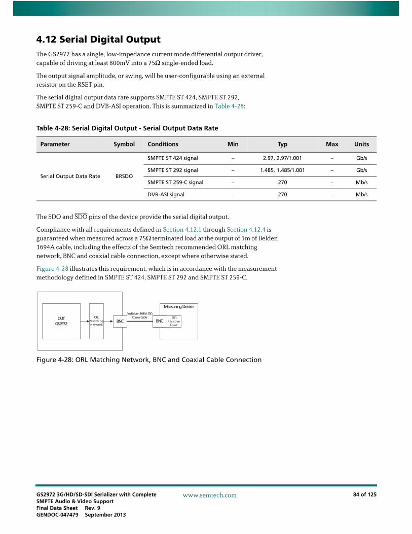
GS2972 3G/HD/SD-SDI Serializer with Complete SMPTE Audio & Video SupportFinal Data Sheet Rev. 9GENDOC-047479 September 2013
84 of 125
www.semtech.com
4.12 Serial Digital OutputThe GS2972 has a single, low-impedance current mode differential output driver, capable of driving at least 800mV into a 75Ω single-ended load.
The output signal amplitude, or swing, will be user-configurable using an external resistor on the RSET pin.
The serial digital output data rate supports SMPTE ST 424, SMPTE ST 292, SMPTE ST 259-C and DVB-ASI operation. This is summarized in Table 4-28:
The SDO and SDO pins of the device provide the serial digital output.
Compliance with all requirements defined in Section 4.12.1 through Section 4.12.4 is guaranteed when measured across a 75Ω terminated load at the output of 1m of Belden 1694A cable, including the effects of the Semtech recommended ORL matching network, BNC and coaxial cable connection, except where otherwise stated.
Figure 4-28 illustrates this requirement, which is in accordance with the measurement methodology defined in SMPTE ST 424, SMPTE ST 292 and SMPTE ST 259-C.
Figure 4-28: ORL Matching Network, BNC and Coaxial Cable Connection
Table 4-28: Serial Digital Output - Serial Output Data Rate
Parameter Symbol Conditions Min Typ Max Units
Serial Output Data Rate BRSDO
SMPTE ST 424 signal − 2.97, 2.97/1.001 − Gb/s
SMPTE ST 292 signal − 1.485, 1.485/1.001 − Gb/s
SMPTE ST 259-C signal − 270 − Mb/s
DVB-ASI signal − 270 − Mb/s
DUTGS2972
ORLMatchingNetwork
BNC
1m Belden 1694A 75ΩCoaxial Cable
BNC75Ω
Resistive Load
Measuring Device

GS2972 3G/HD/SD-SDI Serializer with Complete SMPTE Audio & Video SupportFinal Data Sheet Rev. 9GENDOC-047479 September 2013
85 of 125
www.semtech.com
4.12.1 Output Signal Interface Levels
The Serial Digital Output signals (SDO and SDO pins), of the device meet the amplitude requirements as defined in SMPTE ST 424 for an unbalanced generator (single-ended).
The signal amplitude is controlled to better than +/-7% of the nominal level defined in SMPTE ST 424, when an external 750Ω 1% resistor is connected between the RSET pin of the device and VCC.
The output signal amplitude can be reduced to less than 1/10th of the nominal amplitude, defined above, by increasing the value of the resistor connected between the RSET pin of the device and VCC.
These requirements are met across all ambient temperature and power supply operating conditions described in Section 2.
The output amplitude of the GS2972 can be adjusted by changing the value of the RSET resistor as shown in Table 4-29. For a 800mVpp output a value of 750Ω is required. A ±1% SMT resistor should be used.
The RSET resistor is part of the high speed output circuit of the GS2972. The resistor should be placed as close as possible to the RSET pin. In addition, an anti-pad should be used underneath the resistor.
4.12.2 Overshoot/Undershoot
The serial digital output signal overshoot and undershoot is controlled to be less that 7% of the output signal amplitude, when operating as an unbalanced generator (single-ended).
This requirement is met for nominal signal amplitudes as defined by SMPTE ST 292.
This requirement is met regardless of the output slew rate setting of the device.
This requirement is met across all ambient temperature and power supply operating conditions described in Section 2.
This requirement is summarized in Table 4-30:
Table 4-29: RSET Resistor Value vs. Output Swing
RSET Resistor Values (Ω) Output Swing (mVpp)
995 608
824 734
750 800
680 884
Table 4-30: Serial Digital Output - Overshoot/Undershoot
Parameter Symbol Conditions Min Typ Max Units
Serial output overshoot /undershoot − − − 0 7 %

GS2972 3G/HD/SD-SDI Serializer with Complete SMPTE Audio & Video SupportFinal Data Sheet Rev. 9GENDOC-047479 September 2013
86 of 125
www.semtech.com
4.12.3 Slew Rate Selection
The GS2972 supports two user-selectable output slew rates.
Control of the slew rate is determined by the setting of the RATE_SEL0 input pin.
When this pin is set HIGH, the output slew rate matches the requirements as defined by the SMPTE ST 259-C standard.
When this pin is set LOW, the output slew rate is better than the requirements as defined by the SMPTE ST 424 standard.
These requirements is met across all ambient temperature and power supply operating conditions described in Section 2.
This requirement is summarized in Table 4-31:
4.12.4 Serial Digital Output Mute
When the SDO_EN/DIS pin is LOW, the serial digital output signals of the device become high-impedance, reducing system power.
The serial digital output is also placed in the high-impedance state when the LOCKED pin is LOW, or when the STANDBY pin is HIGH.
Table 4-31: Serial Digital Output - Rise/Fall Time
Parameter Symbol Conditions Min Typ Max Units
Serial Output Rise/Fall Time 20% ~ 80%
SDOTR
SMPTE ST 292/ST 424 signal − − 135 ps
SMPTE ST 259-C signal 400 − 800 ps

GS2972 3G/HD/SD-SDI Serializer with Complete SMPTE Audio & Video SupportFinal Data Sheet Rev. 9GENDOC-047479 September 2013
87 of 125
www.semtech.com
4.13 GSPI Host InterfaceNote: When using more than one Semtech serializer or deserializer (SerDes) in the same design, carefully read this section to see how the GSPI ports of multiple ICs should be connected to each other. Unlike some previous devices, the SDOUT pin of these SerDes ICs is a non-clocked, loop-through of SDIN (allowing for multiple devices to be connected to the GSPI chain). The SDOUT pins of multiple SerDes ICs should not be bussed together, as was the case with some older generations of SerDes ICs.
The GSPI, or Gennum Serial Peripheral Interface, is a 4-wire interface provided to allow the application layer to access additional status information through configuration registers in the GS2972.
The GSPI comprises a Serial Data Input signal (SDIN), Serial Data Output signal (SDOUT), an active-low Chip Select (CS) and a Burst Clock (SCLK).
Because these pins can be shared with the JTAG interface port for compatibility with the GS1582, an additional control signal pin JTAG/HOST is provided.
When JTAG/HOST is LOW, the GSPI interface is enabled. When JTAG/HOST is HIGH, the JTAG interface is enabled.
When operating in GSPI mode, the SCLK, SDIN, and CS signals are provided by the application interface. The SDOUT pin is a non-clocked loop-through of SDIN, and may be connected to the SDIN of another device, allowing multiple devices to be connected to the GSPI chain. The interface is illustrated in Figure 4-29 below.
Figure 4-29: GSPI Application Interface Connection
All read or write access to the GS2972 is initiated and terminated by the application host processor. Each access always begins with a Command/Address Word followed by a data read to or written from the GS2972.
Application Host
SCLK SCLK
SCLK
SDOUT SDIN
SDOUT
SDOUT
SDIN
SDIN
GS2972
GS2972
CS1
CS
CS
CS2

GS2972 3G/HD/SD-SDI Serializer with Complete SMPTE Audio & Video SupportFinal Data Sheet Rev. 9GENDOC-047479 September 2013
88 of 125
www.semtech.com
4.13.1 Command Word Description
The Command Word consists of a 16-bit word transmitted MSB first and contains a read/write bit, an Auto-Increment bit and a 12-bit address. Figure 4-30 shows the command word format and bit configurations.
Command Words are clocked into the GS2972 on the rising edge of the Serial Clock SCLK, which operates in a burst fashion.
When the Auto-Increment bit is set LOW, each Command Word must be followed by only one Data Word to ensure proper operation. If the Auto-Increment bit is set HIGH, the following Data Word will be written into the address specified in the Command Word, and subsequent data words will be written into incremental addresses from the previous Data Word. This facilitates multiple address writes without sending a Command Word for each Data Word.
Figure 4-30: Command Word Format
4.13.2 Data Read or Write Access
Serial data is transmitted or received MSB first synchronous with the rising edge of the Serial Clock, SCLK. The Chip Select (CS) signal must be active LOW a minimum of 1.5ns (t0 in Figure 4-32) before the first clock edge to ensure proper operation.
During a Read sequence (Command Word R/W bit set HIGH), a wait state of 148ns (4 x 1/fPCLK, t5 in Figure 4-32) is required between writing the Command Word and reading the following Data Word. The read bits are clocked out on the negative edges of SCLK.
Note 1: Where several devices are connected to the GSPI chain, only one CS_TMS may be asserted during a read sequence.
During a Write sequence (Command Word R/W bit set LOW), a wait state of 37ns (1 x 1/fPCLK, t4 in Figure 4-32) is required between the Command Word and the following Data Word. This wait state must also be maintained between successive Command Word/Data Word write sequences. When Auto-increment mode is selected (AutoInc = 1), the wait state must be maintained between successive Data Words after the initial Command Word/Data Word sequence.
During the write sequence, all command and following Data Words input at the SDIN pin are output at the SDOUT pin as is.
When several devices are connected to the GSPI chain, data can be written simultaneously to all the devices which have CS set LOW.
Note 2: If the application interface performs a Read or Write access after power-up, prior to the application of a valid serial video input signal, the SCLK frequency must not exceed 10MHz.
Figure 4-31: Data Word Format
A0A1A2A3A4A5A6A7A8A9A11
MSB LSBA10R/W RSV RSV AutoInc
D15 D14 D13 D12 D0D1D2D3D4D5D6D7D8D9D11 D10
MSB LSB

GS2972 3G/HD/SD-SDI Serializer with Complete SMPTE Audio & Video SupportFinal Data Sheet Rev. 9GENDOC-047479 September 2013
89 of 125
www.semtech.com
4.13.3 GSPI Timing
Write and Read Mode timing for the GSPI interface is as shown in the following diagrams:
Figure 4-32: Write Mode
Figure 4-33: Read Mode
Figure 4-34: GSPI Time Delay
SCLK_TCK
CS_TMS
SDIN_TDI
SDOUT_TDO
t0
t3
t1
t2
R/W
t8
t4
t7
R/WAuto_Inc
Auto_Inc
A11
A11
A10
A10
A9
A9
A8
A8
A7
A7
A6
A6 A5
A5 A4
A4
A3
A3
A2
A2
A1
A1
A0
A0
D15
D15
D14
D14
D13
D13
D12
D12
D11
D11
D10
D10
D9
D9
D8
D8
D7
D7
D6
D6
D5
D5
D4
D4
D3
D3
D2
D2
D1
D1
D0
D0RSV
RSVRSV
RSV
SCLK_TCK
CS_TMS
SDIN_TDI
SDOUT_TDO R/W
R/WAuto_Inc
Auto_Inc
A11
A11
A10
A10
A9
A9
A8
A8
A7
A7
A6
A6 A5
A5 A4
A4
A3
A3
A2
A2
A1
A1
A0
A0 D15 D14 D13 D12 D11 D10 D9 D8 D7 D6 D5 D4 D3 D2 D1 D0RSV
RSV
RSV
RSV
t6
t5
SDIN_TDI data_0
SDIN_TDI to SDOUT_TDO combinational path for daisy chain connection of multiple GS2972 devices.
SDOUT_TDO data_0
TDELAY
Table 4-32: GSPI Time Delay
Parameter Symbol Conditions Min Typ Max Units
Delay time tDELAY50% levels;
+1.8V operation− − 10.5 ns
Delay time tDELAY50% levels;
+3.3V operation− − 8.7 ns

GS2972 3G/HD/SD-SDI Serializer with Complete SMPTE Audio & Video SupportFinal Data Sheet Rev. 9GENDOC-047479 September 2013
90 of 125
www.semtech.com
Table 4-33: GSPI AC Characteristics
Parameter Symbol Conditions Min Typ Max Units
CS low before SCLK rising edge
t0
50% levels; +3.3V or +1.8V operation
1.5 − − ns
SCLK period t1 12.5 − − ns
SCLK duty cycle t2 40 50 60 %
Input data setup time t3 1.5 − − ns
Time between end of Command Word (or data in Auto-Increment mode) and the first SCLK of the following Data Word – write cycle.
t4
PCLK (MHz)
ns
− −ns
unlocked 445
13.5 74.2
27.0 37.1
74.25 13.5
148.5 6.7
Time between end of Command Word (or data in Auto-Increment mode) and the first SCLK of the following Data Word – read cycle.
t5
PCLK (MHz)
ns
− − ns
unlocked 1187
13.5 297
27.0 148.5
74.25 53.9
148.5 27
Output hold time (15pF load) t6 1.5 − − ns
CS HIGH after last SCLK rising edge
t7
PCLK (MHz)
ns
− − ns
unlocked 445
74.2 74.2
37.10 37.1
74.25 13.5
148.5 6.7
Input data hold time t8 1.5 − − ns
Note: If the application interface performs a Read or Write access after power-up, prior to the application of a valid serial video input signal, the SCLK frequency must not exceed 10MHz.

GS2972 3G/HD/SD-SDI Serializer with Complete SMPTE Audio & Video SupportFinal Data Sheet Rev. 9GENDOC-047479 September 2013
91 of 125
www.semtech.com
4.14 Host Interface Register Maps
4.14.1 Video Core Registers
Table 4-34: Video Core Configuration and Status Registers
Address Register Name Bit Name Bit Description R/W Default
000h IOPROC
RSVD 15 Reserved. R 0
DELAY_LINE_ENABLE 14HIGH - enables the delay line. LOW - disables the delay line.
R/W 0
AUDIO_LEVELB_STREAM_2_1B 13
HIGH - embeds audio on the DS2 of a 3G Level B signal. LOW - embeds audio on the DS1 of a 3G Level B signal.
R/W 0
EDH_CRC_UPDATE 12
HIGH - preserve incoming EDH flags and insert into outgoing EDH packets. LOW - embed flags from 003 in EDH packet.
R/W 0
ANC_INS 11
HIGH - disable ancillary data insertion. LOW - embeds ANC packet stored at 040h to 13Fh according to parameters at 005h to 02Dh.
R/W 0
AUDIO_EMBED 10HIGH - disable audio embedding. LOW - enables audio embedding.
R/W 0
CONV_372 9
HIGH - disable Level A-B conversion. LOW - enable Level A-B conversion.
R/W 1
H_CONFIG 8
Chooses H configuration;
LOW - Active-line based blanking is enabled. HIGH - SMPTE H timing.
R/W 0
RSVD 7 Reserved. R/W 0
SMPTE_352M_INS 6
HIGH - disables insertion of SMPTE ST 352 packets. LOW - enables insertion of SMPTE ST 352 packets
R/W 0
ILLEGAL_WORD_REMAP 5HIGH - disables illegal word remapping.
R/W 0
EDH_CRC_INS 4HIGH - disables EDH CRC error correction and insertion.
R/W 0
ANC_CSUM_INS 3HIGH - disables insertion of ancillary data checksums.
R/W 0
CRC_INS 2HIGH - disables insertion of HD/3G CRC words.
R/W 0

GS2972 3G/HD/SD-SDI Serializer with Complete SMPTE Audio & Video SupportFinal Data Sheet Rev. 9GENDOC-047479 September 2013
92 of 125
www.semtech.com
000h IOPROC
LNUM_INS 1HIGH = disables insertion of HD/3G line numbers.
R/W 0
TRS_INS 0HIGH = disables insertion of TRS words.
R/W 0
001h ERROR_STAT
RSVD 15-7 Reserved. R 0
TRS_PERR 6TRS protection error.
LOW - No errors in TRS. HIGH - Errors in TRS.
R 0
Y1_EDH_CS_ERR 5Same as CS_ERR but only updates its state when packet being inspected is an EDH packet.
R 0
Y1_CS_ERR 4
HIGH indicates that a checksum error is detected. It is updated every time a CS word is present on the output.
Note: This bit will not be set for CSUM values in the protected ranges (from 000h to 003h and from 3FCh to 3FFh).
R 0
FORMAT_ERR 3HIGH indicates standard is not recognized for 861D conversion.
R 0
TIMING_ERR 2
HIGH indicates that the RASTER measurements do not line up with the extracted ST 352 packet information.
R 0
NO_352M_ERR 1HIGH indicates no ST 352 packet embedded in incoming video.
R 0
LOCK_ERR 0HIGH indicates PLL lock error indication.
R 0
Table 4-34: Video Core Configuration and Status Registers (Continued)
Address Register Name Bit Name Bit Description R/W Default

GS2972 3G/HD/SD-SDI Serializer with Complete SMPTE Audio & Video SupportFinal Data Sheet Rev. 9GENDOC-047479 September 2013
93 of 125
www.semtech.com
002h EDH_FLAG_EXT
RSVD 15 Reserved. R 0
ANC_UES_EXT 14Ancillary data - unknown error status flag.
R 0
ANC_IDA_EXT 13Ancillary data - internal error detected already flag.
R 0
ANC_IDH_EXT 12Ancillary data - internal error detected here flag.
R 0
ANC_EDA_EXT 11Ancillary data - error detected already flag.
R 0
ANC_EDH_EXT 10Ancillary data - error detected here flag.
R 0
FF_UES_EXT 9EDH Full Field - unknown error status flag.
R 0
FF_IDA_EXT 8EDH Full Field - internal error detected already flag.
R 0
FF_IDH_EXT 7EDH Full Field - internal error detected here flag.
R 0
FF_EDA_EXT 6EDH Full Field - error detected already flag.
R 0
FF_EDH_EXT 5EDH Full Field - error detected here flag.
R 0
AP_UES_EXT 4EDH Active Picture - unknown error status flag.
R 0
AP_IDA_EXT 3EDH Active Picture - internal error detected already flag.
R 0
AP_IDH_EXT 2EDH Active Picture - internal error detected here flag.
R 0
AP_EDA_EXT 1EDH Active Picture - error detected already flag.
R 0
AP_EDH_EXT 0EDH Active Picture - error detected here flag.
R 0
Table 4-34: Video Core Configuration and Status Registers (Continued)
Address Register Name Bit Name Bit Description R/W Default

GS2972 3G/HD/SD-SDI Serializer with Complete SMPTE Audio & Video SupportFinal Data Sheet Rev. 9GENDOC-047479 September 2013
94 of 125
www.semtech.com
003h EDH_FLAG_PGM
RSVD 15 Reserved. R 0
ANC_UES_PGM 14Ancillary data - unknown error status flag.
R 0
ANC_IDA_PGM 13Ancillary data - internal error detected already flag.
R/W 0
ANC_IDH_PGM 12Ancillary data - internal error detected here flag.
R/W 0
ANC_EDA_PGM 11Ancillary data - error detected already flag.
R/W 0
ANC_EDH_PGM 10Ancillary data - error detected here flag.
R/W 0
FF_UES_PGM 9EDH Full Field - unknown error status flag.
R/W 0
FF_IDA_PGM 8EDH Full Field - internal error detected already flag.
R/W 0
FF_IDH_PGM 7EDH Full Field - internal error detected here flag.
R/W 0
FF_EDA_PGM 6EDH Full Field - error detected already flag.
R/W 0
FF_EDH_PGM 5EDH Full Field - error detected here flag.
R/W 0
AP_UES_PGM 4EDH Active Picture - unknown error status flag.
R/W 0
AP_IDA_PGM 3EDH Active Picture - internal error detected already flag.
R/W 0
AP_IDH_PGM 2EDH Active Picture - internal error detected here flag.
R/W 0
AP_EDA_PGM 1EDH Active Picture - error detected already flag.
R/W 0
AP_EDH_PGM 0EDH Active Picture - error detected here flag.
R/W 0
004h DATA_FORMAT
RSVD 15-10 Reserved. R 0
VD_STD 9-5 Detected video standard. R 0
INT/PROGB 4HIGH = interlaced signal LOW = progressive signal
R 0
CONV_372_LOCKED 3Convert 372 lock indication. Active HIGH.
R 0
STD_LOCK 2Standard lock indication. Active HIGH.
R 0
V_LOCK 1Vertical lock indication. Active HIGH.
R 0
H_LOCK 0Horizontal lock indication. Active HIGH.
R 0
Table 4-34: Video Core Configuration and Status Registers (Continued)
Address Register Name Bit Name Bit Description R/W Default

GS2972 3G/HD/SD-SDI Serializer with Complete SMPTE Audio & Video SupportFinal Data Sheet Rev. 9GENDOC-047479 September 2013
95 of 125
www.semtech.com
005h RSVD RSVD 15-0 Reserved. R 0
006h VSD_FORCE
RSVD 15-6 Reserved. R 0
VSD_FORCE 5Use the CSR register STD value rather than the flywheels STD value. Active HIGH.
R/W 0
VID_STD_FORCE 4-0 Force VID STD CSR. R/W 0
007h EDH_STATUS
RSVD 15-2 Reserved. R 0
FF_CRC_V 1 Full Field extracted V bit. R 0
AP_CRC_V 0 Active Picture extracted V bit. R 0
008hFIRST_AVAIL_
POSITION
RSVD 15-1 Reserved. R 0
FIRST_AVAIL_POSITION 0
HIGH - ST 352 insertion occurs on first available ANC space. LOW - insert ST 352 packets right after EAV/CRC1.
R/W 1
009h RESERVED RESERVED_7 15-0 Reserved. R 0
00AhVIDEO_FORMAT_352_OUT_WORD_1
VIDEO_FORMAT_OUT_DS1_2 15-8SMPTE ST 352 DS1 embedded packet - byte 2.
R/W 0
VIDEO_FORMAT_OUT_DS1_1 7-0SMPTE ST 352 DS1 embedded packet - byte 1.
R/W 0
00BhVIDEO_FORMAT_352_OUT_WORD_2
VIDEO_FORMAT_OUT_DS1_4 15-8SMPTE ST 352 DS1 embedded packet - byte 4.
R/W 0
VIDEO_FORMAT_OUT_DS1_3 7-0SMPTE ST 352 DS1 embedded packet - byte 3.
R/W 0
00ChVIDEO_FORMAT_352_OUT_WORD_3
VIDEO_FORMAT_OUT_DS2_2 15-8SMPTE ST 352 DS2 embedded packet - byte 2.
R/W 0
VIDEO_FORMAT_OUT_DS2_1 7-0SMPTE ST 352 DS2 embedded packet - byte 1.
R/W 0
00DhVIDEO_FORMAT_352_OUT_WORD_4
VIDEO_FORMAT_OUT_DS2_4 15-8SMPTE ST 352 DS2 embedded packet - byte 4.
R/W 0
VIDEO_FORMAT_OUT_DS2_3 7-0SMPTE ST 352 DS2 embedded packet - byte 3.
R/W 0
00EhVIDEO_FORMAT_3
52_IN_WORD_1
VIDEO_FORMAT_IN_DS1_2 15-8SMPTE ST 352 DS1 extracted packet - byte 2.
R 0
VIDEO_FORMAT_IN_DS1_1 7-0SMPTE ST 352 DS1 extracted packet - byte 1.
R 0
00FhVIDEO_FORMAT_3
52_IN_WORD_2
VIDEO_FORMAT_IN_DS1_4 15-8SMPTE ST 352 DS1 extracted packet - byte 4.
R 0
VIDEO_FORMAT_IN_DS1_3 7-0SMPTE ST 352 DS1 extracted packet - byte 3.
R 0
Table 4-34: Video Core Configuration and Status Registers (Continued)
Address Register Name Bit Name Bit Description R/W Default
GS2972 3G/HD/SD-SDI Serializer with Complete SMPTE Audio & Video SupportFinal Data Sheet Rev. 9GENDOC-047479 September 2013
96 of 125
www.semtech.com
010hVIDEO_FORMAT_3
52_IN_WORD_3
VIDEO_FORMAT_IN_DS2_2 15-8SMPTE ST 352 DS2 extracted packet - byte 2.
R 0
VIDEO_FORMAT_IN_DS2_1 7-0SMPTE ST 352 DS2 extracted packet - byte 1.
R 0
011hVIDEO_FORMAT_3
52_IN_WORD_4
VIDEO_FORMAT_IN_DS2_4 15-8SMPTE ST 352 DS2 extracted packet - byte 4.
R 0
VIDEO_FORMAT_IN_DS2_3 7-0SMPTE ST 352 DS2 extracted packet - byte 3.
R 0
012h RASTER_STRUC_1RSVD 15-11 Reserved. R 0
LINES_PER_FRAME 10-0 Total lines per frame. R 0
013h RASTER_STRUC_2RSVD 15-14 Reserved. R 0
WORDS_PER_LINE 13-0 Total words per line. R 0
014h RASTER_STRUC_3RSVD 15-13 Reserved. R 0
ACTIVE_WORDS_PER_LINE 12-0 Words per active line. R 0
015h RASTER_STRUC_4RSVD 15-11 Reserved. R 0
ACTIVE_LINES_PER_FIELD 10-0 Active lines per frame. R 0
016h to 023h
RSVD RSVD 15-0 Reserved. R 0
024hFIRST_LINE_NUMBER_
STATUS
RSVD 15-2 Reserved. R 0
PACKET_MISSED 1
ANC data packet could not be inserted in its entirety.
HIGH - ANC packet cannot be inserted in it’s entirety.
R 0
RW_CONFLICT 0
Same RAM address was read and written to at the same time.
HIGH - one of the addresses from 040h to 13Fh was read and written to at the same time.
R 0
025hFIRST_LINE_
NUMBER
RSVD 15-12 Reserved. R 0
ANC_INS_MODE 11ANC data insertion mode.
HIGH - Concatenate LOW - Separate
R/W 0
FIRST_LINE_NUMBER 10-0First line number to insert ANC packet on.
R/W 0
Table 4-34: Video Core Configuration and Status Registers (Continued)
Address Register Name Bit Name Bit Description R/W Default

GS2972 3G/HD/SD-SDI Serializer with Complete SMPTE Audio & Video SupportFinal Data Sheet Rev. 9GENDOC-047479 September 2013
97 of 125
www.semtech.com
026hFIRST_LINE_
NUMBER_OF_WORDS
FIRST_LINE_NUMBER_ANC_TYPE
15ANC region to insert packet in HIGH - VANC, LOW - HANC.
R/W 0
FIRST_LINE_NUMBER_STREAM_TYPE
14Stream to insert packet in
HIGH - C stream, LOW - Y stream.
R/W 0
RSVD 13-10 Reserved. R 0
FIRST_LINE_NUMBER_OF_WORDS
9-0Total number of words in ANC packet to be inserted in first line.
R/W 0
027hSECOND_LINE_
NUMBER
RSVD 15-11 Reserved. R 0
SECOND_LINE_NUMBER 10-0Second line number to insert ANC packet on in Separate Line mode.
R/W 0
028hSECOND_LINE_NUMBER_OF_
WORDS
SECOND_LINE_NUMBER_ANC_TYPE
15ANC region to insert packet in. HIGH - VANC, LOW - HANC.
R/W 0
SECOND_LINE_NUMBER_STREAM_TYPE
14Stream to insert packet in.
HIGH - C stream, LOW - Y stream.
R/W 0
RSVD 13-10 Reserved. R 0
SECOND_LINE_NUMBER_OF_WORDS
9-0Total number of words in ANC packet to be inserted in second line.
R/W 0
029hTHIRD_LINE_
NUMBER
RSVD 15-11 Reserved. R 0
THIRD_LINE_NUMBER 10-0Third line number to insert ANC packet on in Separate Line mode.
R/W 0
02AhTHIRD_LINE_NUMBER_OF_
WORDS
THIRD_LINE_NUMBER_ANC_TYPE
15ANC region to insert packet in. HIGH - VANC, LOW - HANC.
R/W 0
THIRD_LINE_NUMBER_STREAM_TYPE
14Stream to insert packet in.
HIGH - C stream, LOW - Y stream.
R/W 0
RSVD 13-10 Reserved. R 0
THIRD_LINE_NUMBER_OF_WORDS
9-0Total number of words in ANC packet to be inserted in third line.
R/W 0
02BhFOURTH_LINE_
NUMBER
RSVD 15-11 Reserved. R 0
FOURTH_LINE_NUMBER 10-0Fourth line number to insert ANC packet on in Seperate Line mode.
R/W 0
Table 4-34: Video Core Configuration and Status Registers (Continued)
Address Register Name Bit Name Bit Description R/W Default
GS2972 3G/HD/SD-SDI Serializer with Complete SMPTE Audio & Video SupportFinal Data Sheet Rev. 9GENDOC-047479 September 2013
98 of 125
www.semtech.com
02ChFOURTH_LINE_NUMBER_OF_
WORDS
FOURTH_LINE_NUMBER_ANC_TYPE
15ANC region to insert packet in HIGH - VANC, LOW - HANC.
R/W 0
FOURTH_LINE_NUMBER_STREAM_TYPE
14Stream to insert packet in.
HIGH - C stream, LOW - Y stream.
R/W 0
RSVD 13-10 Reserved. R 0
FOURTH_LINE_NUMBER_OF_WORDS
9-0Total number of words in ANC packet to be inserted in fourth line.
R/W 0
02Dh STREAM_TYPE_1
RSVD 15-5 Reserved. R 0
EDH_LINE_CHECK_EN 4
HIGH - ANC block will not insert data into the EDH region of the HANC space. LOW - ANC block will insert data into the EDH region.
R/W 1
STREAM_TYPE1_LINE_4 3
HIGH - data for the fourth line in separate mode is inserted into Data Stream Two. LOW - Data Stream One. Parameter only applicable for 3G.
R/W 0
STREAM_TYPE1_LINE_3 2
HIGH - data for the third line in separate mode is inserted into Data Stream Two. LOW - Data Stream One. Parameter only applicable for 3G.
R/W 0
STREAM_TYPE1_LINE_2 1
HIGH - data for the second line in separate mode is inserted into Data Stream Two. LOW - Data Stream One. Parameter only applicable for 3G.
R/W 0
STREAM_TYPE1_LINE_1 0
HIGH - data for the first line in separate mode is inserted into Data Stream Two. LOW - Data Stream One. Parameter only applicable for 3G.
R/W 0
02Eh to 03Fh
RSVD RSVD 15-0 Reserved. R 0
040h to 07Fh
ANC_PACKET_BANK_1
ANC_PACKET_BANK 15-0
First bank of user-defined 8-bit ancillary data.
Bit 15 - 8: 2nd byte (MSB to LSB) Bit 7 - 0: 1st byte (MSB to LSB)
See 4.8 ANC Data Insertion.
− −
080h to 0BFh
ANC_PACKET_BANK_2
ANC_PACKET_BANK 15-0
Second bank of user-defined 8-bit ancillary data.
Bit 15 - 8: 2nd byte (MSB to LSB) Bit 7 - 0: 1st byte (MSB to LSB)
See 4.8 ANC Data Insertion.
− −
Table 4-34: Video Core Configuration and Status Registers (Continued)
Address Register Name Bit Name Bit Description R/W Default

GS2972 3G/HD/SD-SDI Serializer with Complete SMPTE Audio & Video SupportFinal Data Sheet Rev. 9GENDOC-047479 September 2013
99 of 125
www.semtech.com
0C0h to 0FFh
ANC_PACKET_BANK_3
ANC_PACKET_BANK 15-0
Third bank of user-defined 8-bit ancillary data.
Bit 15 - 8: 2nd byte (MSB to LSB) Bit 7 - 0: 1st byte (MSB to LSB)
See 4.8 ANC Data Insertion.
− −
100h to 13Fh
ANC_PACKET_BANK_4
ANC_PACKET_BANK 15-0
Fourth bank of user-defined 8-bit ancillary data.
Bit 15 - 8: 2nd byte (MSB to LSB) Bit 7 - 0: 1st byte (MSB to LSB)
See 4.8 ANC Data Insertion.
− −
140h to 209h
RSVD RSVD − Reserved. R 0
20Ah SDTI_TDM
RSVD 15-8 Reserved. R 0
SDTI_TDM_DS2 7HIGH indicates an SDTI type signal on input for Data Stream Two.
R/W 0
SDTI_TDM_DS1 6HIGH indicates an SDTI type signal on input for Data Stream One.
R/W 0
RSVD 5-0 Reserved. R 0
20Bh to 20Ch
RSVD RSVD − Reserved. R 0
20Dh LEVELB_INDICATION
RSVD 15-9 Reserved. R 0
LEVEL_B 8HIGH indicates level B detected. Only relevant for 3G input streams.
R 0
RSVD 7-0 Reserved. R 0
20Eh DRIVE_STRENGTH
RSVD 15-6 Reserved. R/W 0
AUDIO_INT_DS 5-4
Drive strength value for AUDIO_INT pin.
00: 4mA; 01: 6mA; 10: 8mA(+1.8V), 10mA(+3.3V); 11: 10mA(+1.8V), 12mA(+3.3V)
R/W 0
LOCKED_DS 3-2
Drive strength value for LOCKED pin.
00: 4mA; 01: 6mA; 10: 8mA(+1.8V), 10mA(+3.3V); 11: 10mA(+1.8V), 12mA(+3.3V)
R/W 0
SDOUT_TDO_DS 1-0
Drive strength value for SDOUT_TDO pin.
00: 4mA; 01: 6mA; 10: 8mA(+1.8V), 10mA(+3.3V); 11: 10mA(+1.8V), 12mA(+3.3V)
R/W 2
20Fh RSVD RSVD 15-0 Reserved. R/W 0
Table 4-34: Video Core Configuration and Status Registers (Continued)
Address Register Name Bit Name Bit Description R/W Default

GS2972 3G/HD/SD-SDI Serializer with Complete SMPTE Audio & Video SupportFinal Data Sheet Rev. 9GENDOC-047479 September 2013
100 of 125
www.semtech.com
4.14.2 SD Audio Core
210h DRIVE_STRENGTH2TDO_DS 15-14
Drive strength value for TDO pin.
00: 4mA; 01: 6mA; 10: 8mA(+1.8V), 10mA(+3.3V); 11: 10mA(+1.8V), 12mA(+3.3V)
R/W 0
RSVD 13-0 Reserved. R/W 0
211h to 232h
RSVD RSVD 15-0 Reserved. R 0
Table 4-34: Video Core Configuration and Status Registers (Continued)
Address Register Name Bit Name Bit Description R/W Default
Table 4-35: SD Audio Core Configuration and Status Registers
Address Register Name Bit Name Bit Description R/W Default
400h CFG_AUD
CTR_AGR 15
Selects replacement of audio control packets.
LOW - Do not replace audio control packets HIGH - Replace all audio control packets
R/W 0
AGR 14Selects Audio Group Replacement operating mode. Active HIGH.
R/W 0
ONE_AGR 13
Specifies the replacement of just the primary group.
LOW - Replace both the primary and secondary groups HIGH - Replace only the primary group
R/W 0
CTRB_ON 12Specifies the embedding of the secondary group audio control packets. Active HIGH.
R/W 1
CLEAR_AUDIO 11Clears all audio FIFO buffers and puts them in the start-up state. Active HIGH.
R/W 0
AFNB_AUTO 10Enables Secondary group audio frame number generation. Active HIGH.
R/W 1
CTRA_ON 9Specifies the embedding of primary group audio control packets. Active HIGH.
R/W 1
AUDIO_24BIT 8
Specifies the sample size for embedded audio.
HIGH - 24-bit LOW - 20-bit/16-bit
R/W 0

GS2972 3G/HD/SD-SDI Serializer with Complete SMPTE Audio & Video SupportFinal Data Sheet Rev. 9GENDOC-047479 September 2013
101 of 125
www.semtech.com
400h CFG_AUD
AFNA_AUTO 7Enables Primary group audio frame number generation. Active HIGH.
R/W 1
AFN_OFS 6-4Offset to add to generated Audio Frame Number. Must be in the range of 0 to 4.
R/W 0
IDB 3-2
Specifies the secondary audio group to embed. Note: Should IDA and IDB be set to the same value, they automatically revert to their default values.
R/W 1
IDA 1-0
Specifies the primary audio group to embed. Note: Should IDA and IDB be set to the same value, they automatically revert to their default values.
R/W 0
401h FIFO_BUF_SIDE
RSVD 15-3 Reserved. R 0
OFFSET_DISABLE 2
Set to disable staggering of secondary group audio sample distribution by one line. Active HIGH.
R/W 0
OS_SEL 1-0
Specifies the audio FIFO buffer size.
00-52 samples deep, 26 sample start-up count 01-24 samples deep, 12 sample start-up count 10-12 samples deep, 6 sample start-up count 11-Reserved
R/W 0
402hAES_EBU_ERR_
STATUS
RSVD 15-4 Reserved. R 0
AES_ERRD 3
Stereo Pair D (7&8) audio input parity error when using AES format. Automatically cleared when read.
R 0
AES_ERRC 2
Stereo Pair C (5&6) audio input parity error when using AES format. Automatically cleared when read.
R 0
AES_ERRB 1
Stereo Pair B (3&4) audio input parity error when using AES format. Automatically cleared when read.
R 0
AES_ERRA 0
Stereo Pair A (1&2) audio input parity error when using AES format. Automatically cleared when read.
R 0
Table 4-35: SD Audio Core Configuration and Status Registers (Continued)
Address Register Name Bit Name Bit Description R/W Default

GS2972 3G/HD/SD-SDI Serializer with Complete SMPTE Audio & Video SupportFinal Data Sheet Rev. 9GENDOC-047479 September 2013
102 of 125
www.semtech.com
403hCHANNEL_STAT_
REGEN
RSVD 15-1 Reserved. R 0
ACS_REGEN 0
Specifies that Audio Channel Status of all channels should be replaced with ACSR[183:0] field.
LOW: Do not replace Channel Status HIGH: Replace Channel Status of all channels
R/W 0
404hPACKET_DET_
STATUS
RSVD 15-14 Reserved. R 0
AXPG4_DET 13Set while Group 4 audio extended packets are detected.
R 0
AXPG3_DET 12Set while Group 3 audio extended packets are detected.
R 0
AXPG2_DET 11Set while Group 2 audio extended packets are detected.
R 0
AXPG1_DET 10Set while Group 1 audio extended packets are detected.
R 0
ACPG4_DET 9Set while Group 4 audio control packets are detected.
R 0
ACPG3_DET 8Set while Group 3 audio control packets are detected.
R 0
ACPG2_DET 7Set while Group 2 audio control packets are detected.
R 0
ACPG1_DET 6Set while Group 1 audio control packets are detected.
R 0
ADPG4_DET 5Set while Group 4 audio data packets are detected.
R 0
ADPG3_DET 4Set while Group 3 audio data packets are detected.
R 0
ADPG2_DET 3Set while Group 2 audio data packets are detected.
R 0
ADPG1_DET 2Set while Group 1 audio data packets are detected.
R 0
ACS_APPLY_WAITB 1
Set while the GS2972 is waiting for a status boundary in the Secondary group before applying the ACSR[183:0] data to that group.
R 0
ACS_APPLY_WAITA 0
ACS_APPLY_WAITA: Set while the GS2972 is waiting for a status boundary in Primary group before applying the ACSR[183:0] data.
R 0
Table 4-35: SD Audio Core Configuration and Status Registers (Continued)
Address Register Name Bit Name Bit Description R/W Default

GS2972 3G/HD/SD-SDI Serializer with Complete SMPTE Audio & Video SupportFinal Data Sheet Rev. 9GENDOC-047479 September 2013
103 of 125
www.semtech.com
405hAES_EBU_ERR_
STATUS1
RSVD 15-6 Reserved. R 0
FINAL_HELD_ASD_ERR 5Final audio sample distribution error.
R 0
HELD_ASD_ERR 4 Audio sample distribution error. R 0
HELD_AES_ERR 3-0AES received errors for the 4 audio lines.
R 0
406h CASCADE
RSVD 15-1 Reserved. R 0
EN_CASCADE 0If HIGH, puts the GS2972 into cascade mode. This bit is only effective if the AGR bit = LOW.
R/W 0
407h to 40Ah
RSVD RSVD 15-0 Reserved. R 0
40BhSERIAL_AUDIO_
FORMAT
AMD 15-14
Audio input format selector for Stereo Pair D input channels 7 and 8. 00: AES/EBU 01: Serial Left Justified 10: Serial Right Justified 11: I2S
R/W 3
AMC 13-12Audio input format selector for Stereo Pair C input channels 5 and 6. (See above for decoding).
R/W 3
AMB 11-10Audio input format selector for Stereo Pair B input channels 3 and 4. (See above for decoding).
R/W 3
AMA 9-8Audio input format selector for Stereo Pair A input channels 1 and 2. (See above for decoding).
R/W 3
MUTE8 7Audio input channel 8 mute enable. Active HIGH.
R/W 0
MUTE7 6Audio input channel 7 mute enable. Active HIGH.
R/W 0
MUTE6 5Audio input channel 6 mute enable. Active HIGH.
R/W 0
MUTE5 4Audio input channel 5 mute enable. Active HIGH.
R/W 0
MUTE4 3Audio input channel 4 mute enable. Active HIGH.
R/W 0
MUTE3 2Audio input channel 3 mute enable. Active HIGH.
R/W 0
MUTE2 1Audio input channel 2 mute enable. Active HIGH.
R/W 0
MUTE1 0Audio input channel 1 mute enable. Active HIGH.
R/W 0
Table 4-35: SD Audio Core Configuration and Status Registers (Continued)
Address Register Name Bit Name Bit Description R/W Default

GS2972 3G/HD/SD-SDI Serializer with Complete SMPTE Audio & Video SupportFinal Data Sheet Rev. 9GENDOC-047479 September 2013
104 of 125
www.semtech.com
40ChCHANNEL_XP_
GRPA
RSVD 15 Reserved. R 0
GPA_WCLK_SRC 14-12
Primary Audio group word clock source selector.
Input channel 1 000 Input channel 2 001 Input channel 3 010 Input channel 4 011 Input channel 5 100 Input channel 6 101 Input channel 7 110 Input channel 8 111
R/W 0
GPA_CH4_SRC 11-9Primary Audio group channel 4 source selector. 011.
R/W 3
GPA_CH3_SRC 8-6Primary Audio group channel 3 source selector. 010.
R/W 2
GPA_CH2_SRC 5-3Primary Audio group channel 2 source selector. 001.
R/W 1
GPA_CH1_SRC 2-0Primary Audio group channel 1 source selector. 000 - Input channel
R/W 0
40DhCHANNEL_XP_
GRPB
RSVD 15 Reserved. R 0
GPB_WCLK_SRC 14-12Secondary Audio group word clock source selector.
R/W 4
GPB_CH4_SRC 11-9Secondary Audio group channel 4 source selector.
R/W 7
GPB_CH3_SRC 8-6Secondary Audio group channel 3 source selector.
R/W 6
GPB_CH2_SRC 5-3Secondary Audio group channel 2 source selector.
R/W 5
GPB_CH1_SRC 2-0Secondary Audio group channel 1 source selector.
R/W 4
Table 4-35: SD Audio Core Configuration and Status Registers (Continued)
Address Register Name Bit Name Bit Description R/W Default

GS2972 3G/HD/SD-SDI Serializer with Complete SMPTE Audio & Video SupportFinal Data Sheet Rev. 9GENDOC-047479 September 2013
105 of 125
www.semtech.com
40Eh INTERRUPT_MASK
EN_ASD_ERR 15 Asserts ASD error flag. R/W 0
EN_NO_VIDEO 14Mask bit when the video format is unknown.
R/W 0
EN_MUX_ERRB 13Asserts AUDIO_INT when the MUX_ERRB flag is set.
R/W 0
EN_MUX_ERRA 12Asserts AUDIO_INT when the MUX_ERRA flag is set.
R/W 0
EN_AES_ERRD 11Asserts AUDIO_INT when the AES_ERRD flag is set.
R/W 0
EN_AES_ERRC 10Asserts AUDIO_INT when the AES_ERRC flag is set.
R/W 0
EN_AES_ERRB 9Asserts AUDIO_INT when the AES_ERRB flag is set.
R/W 0
EN_AES_ERRA 8Asserts AUDIO_INT when the AES_ERRA flag is set.
R/W 0
EN_ACPG4_DET 7Asserts AUDIO_INT when the ACPG4_DET flag is set.
R/W 0
EN_ACPG3_DET 6Asserts AUDIO_INT when the ACPG3_DET flag is set.
R/W 0
EN_ACPG2_DET 5Asserts AUDIO_INT when the ACPG2_DET flag is set.
R/W 0
EN_ACPG1_DET 4Asserts AUDIO_INT when the ACPG1_DET flag is set.
R/W 0
EN_ADPG4_DET 3Asserts AUDIO_INT when the ADPG4_DET flag is set.
R/W 0
EN_ADPG3_DET 2Asserts AUDIO_INT when the ADPG3_DET flag is set.
R/W 0
EN_ADPG2_DET 1Asserts AUDIO_INT when the ADPG2_DET flag is set.
R/W 0
EN_ADPG1_DET 0Asserts AUDIO_INT when the ADPG1_DET flag is set.
R/W 0
Table 4-35: SD Audio Core Configuration and Status Registers (Continued)
Address Register Name Bit Name Bit Description R/W Default

GS2972 3G/HD/SD-SDI Serializer with Complete SMPTE Audio & Video SupportFinal Data Sheet Rev. 9GENDOC-047479 September 2013
106 of 125
www.semtech.com
40Fh ACTIVE_CHANNEL
RSVD 15-13 Reserved. R 0
MUTE_ALL 12 Mutes all input audio channels. R/W 0
LSB_FIRSTD 11
Causes the fourth stereo pair serial input formats to use LSB first. Used in conjunction with AMD, and only relevant when AMD is 01 or 10 Figure 4-16 to 4-19.
R/W 0
LSB_FIRSTC 10
Causes the third stereo pair serial input formats to use LSB first. Used in conjunction with AMCand only relevant when AMC is 01 or 10 Figure 4-16 to 4-19.
R/W 0
LSB_FIRSTB 9
Causes the second stereo pair serial input formats to use LSB first. Used in conjunction with AMB and only relevant when AMD is 01 or 10 Figure 4-16 to 4-19.
R/W 0
LSB_FIRSTA 8
Causes the first stereo pair serial input formats to use LSB first. Used in conjunction with AMA and only relevant when AMA is 01 or 10 Figure 4-16 to 4-19.
R/W 0
ACT8 7Specifies embedding of secondary audio group channel 8. Active HIGH.
R/W 1
ACT7 6Specifies embedding of secondary audio group channel 7. Active HIGH.
R/W 1
ACT6 5Specifies embedding of secondary audio group channel 6. Active HIGH.
R/W 1
ACT5 4Specifies embedding of secondary audio group channel 5. Active HIGH.
R/W 1
ACT4 3Specifies embedding of primary audio group channel 4. Active HIGH.
R/W 1
ACT3 2Specifies embedding of primary audio group channel 3. Active HIGH.
R/W 1
ACT2 1Specifies embedding of primary audio group channel 2. Active HIGH.
R/W 1
ACT1 0Specifies embedding of primary audio group channel 1. Active HIGH.
R/W 1
Table 4-35: SD Audio Core Configuration and Status Registers (Continued)
Address Register Name Bit Name Bit Description R/W Default
GS2972 3G/HD/SD-SDI Serializer with Complete SMPTE Audio & Video SupportFinal Data Sheet Rev. 9GENDOC-047479 September 2013
107 of 125
www.semtech.com
410h XPOINT_ERROR
RSVD 15-3 Reserved. R 0
MUX_ERRB 2
Set in Cascade mode when the incoming video contains packets with the same group number as the Secondary Group.
R 0
MUX_ERRA 1
Set in Cascade mode when the incoming video contains packets with the same group number as the Primary Group.
R 0
XPOINT_ERROR 0
Set when the crosspoint switch is configured to put the same audio channel in both Primary and Secondary Groups.
R 0
411h to 41Fh
RSVD RSVD − Reserved. R 0
420h CHANNEL_STATUS_REG_1
RSVD 15-8 Reserved. R 0
ACSR_BYTE_1 7-0 Audio channel status block byte 1. R/W 133
421h CHANNEL_STATUS_REG_2
RSVD 15-8 Reserved. R 0
ACSR_BYTE_2 7-0 Audio channel status block byte 2. R/W 8
422h CHANNEL_STATUS_REG_3
ACSR_BYTE_4 15-8 Audio channel status block byte 4. R/W 0
ACSR_BYTE_3 7-0 Audio channel status block byte 3. R/W 44
423h CHANNEL_STATUS_REG_4
ACSR_BYTE_6 15-8 Audio channel status block byte 6. R/W 0
ACSR_BYTE_5 7-0 Audio channel status block byte 5. R/W 0
424h CHANNEL_STATUS_REG_5
ACSR_BYTE_8 15-8 Audio channel status block byte 8. R/W 0
ACSR_BYTE_7 7-0 Audio channel status block byte 7. R/W 0
425h CHANNEL_STATUS_REG_6
ACSR_BYTE_10 15-8Audio channel status block byte 10.
R/W 0
ACSR_BYTE_9 7-0 Audio channel status block byte 9. R/W 0
426h CHANNEL_STATUS_REG_7
ACSR_BYTE_12 15-8Audio channel status block byte 12.
R/W 0
ACSR_BYTE_11 7-0Audio channel status block byte 11.
R/W 0
427h CHANNEL_STATUS_REG_8
ACSR_BYTE_14 15-8Audio channel status block byte 14.
R/W 0
ACSR_BYTE_13 7-0Audio channel status block byte 13.
R/W 0
428h CHANNEL_STATUS_REG_9
ACSR_BYTE_16 15-8Audio channel status block byte 16.
R/W 0
ACSR_BYTE_15 7-0Audio channel status block byte 15.
R/W 0
Table 4-35: SD Audio Core Configuration and Status Registers (Continued)
Address Register Name Bit Name Bit Description R/W Default

GS2972 3G/HD/SD-SDI Serializer with Complete SMPTE Audio & Video SupportFinal Data Sheet Rev. 9GENDOC-047479 September 2013
108 of 125
www.semtech.com
429h CHANNEL_STATUS_REG_10
ACSR_BYTE_18 15-8Audio channel status block byte 18.
R/W 0
ACSR_BYTE_17 7-0Audio channel status block byte 17.
R/W 0
42Ah CHANNEL_STATUS_REG_11
ACSR_BYTE_20 15-8Audio channel status block byte 20.
R/W 0
ACSR_BYTE_19 7-0Audio channel status block byte 19.
R/W 0
42Bh CHANNEL_STATUS_REG_12
ACSR_BYTE_22 15-8Audio channel status block byte 22.
R/W 0
ACSR_BYTE_21 7-0Audio channel status block byte 21.
R/W 0
42Ch CHANNEL_STATUS_REG_13
RSVD 15-8 Reserved. R/W 0
ACSR_BYTE_23 7-0Audio channel status block byte 23.
R/W 0
42Dh to 43Fh
RSVD RSVD − Reserved. R 0
440hAUDIO_CTRL_GRPA_REG_1
RSVD 15-9 Reserved. R 0
DEL1A_BYTE_1 8-1Primary Audio group delay data for channel 1 byte 1.
R/W 0
EBIT1A 0
Primary Audio group delay data for channel 1. HIGH - indicates delay specified at DEL1A_BYTE_1 is valid. See SMPTE ST 272 for additional information.
R/W 0
441hAUDIO_CTRL_GRPA_REG_2
RSVD 15-9 Reserved. R 0
DEL1A_BYTE_2 8-0Primary Audio group delay data for channel 1 byte 2.
R/W 0
442hAUDIO_CTRL_GRPA_REG_3
RSVD 15-9 Reserved. R 0
DEL1A_BYTE_3 8-0Primary Audio group delay data for channel 1 byte 3.
R/W 0
443hAUDIO_CTRL_GRPA_REG_4
RSVD 15-9 Reserved. R 0
DEL2A_BYTE_1 8-1Primary Audio group delay data for channel 2 byte 1.
R/W 0
EBIT2A 0Primary Audio group delay data valid flag for channel 2.
R/W 0
444hAUDIO_CTRL_GRPA_REG_5
RSVD 15-9 Reserved. R 0
DEL2A_BYTE_2 8-0Primary Audio group delay data for channel 2 byte 2.
R/W 0
445hAUDIO_CTRL_GRPA_REG_6
RSVD 15-9 Reserved. R 0
DEL2A_BYTE_3 8-0Primary Audio group delay data for channel 2 byte 3.
R/W 0
Table 4-35: SD Audio Core Configuration and Status Registers (Continued)
Address Register Name Bit Name Bit Description R/W Default

GS2972 3G/HD/SD-SDI Serializer with Complete SMPTE Audio & Video SupportFinal Data Sheet Rev. 9GENDOC-047479 September 2013
109 of 125
www.semtech.com
446hAUDIO_CTRL_GRPA_REG_7
RSVD 15-9 Reserved. R 0
DEL3A_BYTE_1 8-1Primary Audio group delay data for channel 3 byte 1.
R/W 0
EBIT3A 0Primary Audio group delay data valid flag for channel 3.
R/W 0
447hAUDIO_CTRL_GRPA_REG_8
RSVD 15-9 Reserved. R 0
DEL3A_BYTE_2 8-0Primary Audio group delay data for channel 3 byte 2.
R/W 0
448hAUDIO_CTRL_GRPA_REG_9
RSVD 15-9 Reserved. R 0
DEL3A_BYTE_3 8-0Primary Audio group delay data for channel 3 byte 3.
R/W 0
449hAUDIO_CTRL_GRPA_REG_10
RSVD 15-9 Reserved. R 0
DEL4A_BYTE_1 8-1Primary Audio group delay data for channel 4 byte 1.
R/W 0
EBIT4A 0Primary Audio group delay data valid flag for channel 4.
R/W 0
44AhAUDIO_CTRL_GRPA_REG_11
RSVD 15-9 Reserved. R 0
DEL4A_BYTE_2 8-0Primary Audio group delay data for channel 4 byte 2.
R/W 0
44BhAUDIO_CTRL_GRPA_REG_12
RSVD 15-9 Reserved. R 0
DEL4A_BYTE_3 8-0Primary Audio group delay data for channel 4 byte 3.
R/W 0
44ChAUDIO_CTRL_GRPB_REG_1
RSVD 15-9 Reserved. R 0
DEL1B_BYTE_1 8-1Secondary Audio group delay data for channel 1 byte 1.
R/W 0
EBIT1B 0Secondary Audio group delay data valid flag for channel 1.
R/W 0
44DhAUDIO_CTRL_GRPB_REG_2
RSVD 15-9 Reserved. R 0
DEL1B_BYTE_2 8-0Secondary Audio group delay data for channel 1 byte 2.
R/W 0
44EhAUDIO_CTRL_GRPB_REG_3
RSVD 15-9 Reserved. R 0
DEL1B_BYTE_3 8-0Secondary Audio group delay data for channel 1 byte 3.
R/W 0
44FhAUDIO_CTRL_GRPB_REG_4
RSVD 15-9 Reserved. R 0
DEL2B_BYTE_1 8-1Secondary Audio group delay data for channel 2 byte 1.
R/W 0
EBIT2B 0Secondary Audio group delay data valid flag for channel 2.
R/W 0
Table 4-35: SD Audio Core Configuration and Status Registers (Continued)
Address Register Name Bit Name Bit Description R/W Default

GS2972 3G/HD/SD-SDI Serializer with Complete SMPTE Audio & Video SupportFinal Data Sheet Rev. 9GENDOC-047479 September 2013
110 of 125
www.semtech.com
450hAUDIO_CTRL_GRPB_REG_5
RSVD 15-9 Reserved. R 0
DEL2B_BYTE_2 8-0Secondary Audio group delay data for channel 2 byte 2.
R/W 0
451hAUDIO_CTRL_GRPB_REG_6
RSVD 15-9 Reserved. R 0
DEL2B_BYTE_3 8-0Secondary Audio group delay data for channel 2 byte 3.
R/W 0
452hAUDIO_CTRL_GR
PB_REG_7
RSVD 15-9 Reserved. R 0
DEL3B_BYTE_1 8-1Secondary Audio group delay data for channel 3 byte 1.
R/W 0
EBIT3B 0Secondary Audio group delay data valid flag for channel 3.
R/W 0
453hAUDIO_CTRL_GR
PB_REG_8
RSVD 15-9 Reserved. R 0
DEL3B_BYTE_2 8-0Secondary Audio group delay data for channel 3 byte 2.
R/W 0
454hAUDIO_CTRL_GR
PB_REG_9
RSVD 15-9 Reserved. R 0
DEL3B_BYTE_3 8-0Secondary Audio group delay data for channel 3 byte 3.
R/W 0
455hAUDIO_CTRL_GR
PB_REG_10
RSVD 15-9 Reserved. R 0
DEL4B_BYTE_1 8-1Secondary Audio group delay data for channel 4 byte 1.
R/W 0
EBIT4B 0Secondary Audio group delay data valid flag for channel 4.
R/W 0
456hAUDIO_CTRL_GR
PB_REG_11
RSVD 15-9 Reserved. R 0
DEL4B_BYTE_2 8-0Secondary Audio group delay data for channel 4 byte 2.
R/W 0
457hAUDIO_CTRL_GR
PB_REG_12
RSVD 15-9 Reserved. R 0
DEL4B_BYTE_3 8-0Secondary Audio group delay data for channel 4 byte 3.
R/W 0
Table 4-35: SD Audio Core Configuration and Status Registers (Continued)
Address Register Name Bit Name Bit Description R/W Default

GS2972 3G/HD/SD-SDI Serializer with Complete SMPTE Audio & Video SupportFinal Data Sheet Rev. 9GENDOC-047479 September 2013
111 of 125
www.semtech.com
4.14.3 HD and 3G Audio Core Registers
Table 4-36: HD and 3G Audio Core Configuration and Status Registers
Address Register Name Bit Name Bit Description R/W Default
800h CFG_AUD
CTR_AGR 15
Selects replacement of audio control packets.
LOW - Do not replace audio control packets HIGH - Replace all audio control packets
R/W 0
AGR 14Selects Audio Group Replacement operating mode. Active HIGH.
R/W 0
ONE_AGR 13
Specifies the replacement of just the primary group.
LOW - Replace both the primary and secondary groups. HIGH - Replace only the primary group.
R/W 0
CTRB_ON 12Specifies the embedding of the secondary group audio control packets. Active HIGH.
R/W 1
ASXB 11Secondary Group asynchronous mode. Active HIGH.
R/W 0
AFNB_AUTO 10Enables Secondary group audio frame number generation. Active HIGH.
R/W 1
CTRA_ON 9Specifies the embedding of primary group audio control packets. Active HIGH.
R/W 1
ASXA 8 Primary Group asynchronous mode. R/W 0
AFNA_AUTO 7Enables Primary group audio frame number generation.
R/W 1
ANF_OFS 6-4Offset to add to generated Audio Frame Number. Must be in the range of 0 to 4.
R/W 0
IDB 3-2
Specifies the Secondary audio group to embed.
00: Audio group #1 01: Audio group #2 10: Audio group #3 11: Audio group #4
R/W 1
IDA 1-0
Specifies the Primary audio group to embed.
00: Audio group #1 01: Audio group #2 10: Audio group #3 11: Audio group #4
R/W 0
801h RSVD RSVD 15-0 Reserved. R 0

GS2972 3G/HD/SD-SDI Serializer with Complete SMPTE Audio & Video SupportFinal Data Sheet Rev. 9GENDOC-047479 September 2013
112 of 125
www.semtech.com
802hCHANNEL_STAT_
REGREN
RSVD 15-1 Reserved. R 0
ACS_REGEN 0
Specifies that Audio Channel Status of all channels should be replaced with ACSR[183:0] field.
LOW: Do not replace Channel Status HIGH: Replace Channel Status of all channels
R/W 0
803hPACKET_DET_
STATUS
RSVD 15-14 Reserved. R 0
AES_ERRD 13Stereo Pair D audio input parity error when using AES format. Automatically cleared when read.
R 0
AES_ERRC 12Stereo Pair C audio input parity error when using AES format. Automatically cleared when read.
R 0
AES_ERRB 11Stereo Pair B audio input parity error when using AES format. Automatically cleared when read.
R 0
AES_ERRA 10Stereo Pair A audio input parity error when using AES format. Automatically cleared when read.
R 0
ACPG4_DET 9Set while Group 4 audio control packets are detected.
R 0
ACPG3_DET 8Set while Group 3 audio control packets are detected.
R 0
ACPG2_DET 7Set while Group 2 audio control packets are detected.
R 0
ACPG1_DET 6Set while Group 1 audio control packets are detected.
R 0
ADPG4_DET 5Set while Group 4 audio data packets are detected.
R 0
ADPG3_DET 4Set while Group 3 audio data packets are detected.
R 0
ADPG2_DET 3Set while Group 2 audio data packets are detected.
R 0
ADPG1_DET 2Set while Group 1 audio data packets are detected.
R 0
ACS_APPLY_WAITB 1
Set while the GS2972 is waiting for a status boundary in the Secondary group before applying the ACSR[183:0] data to that group.
R 0
803hPACKET_DET_
STATUSACS_APPLY_WAITA 0
ACS_APPLY_WAITA: Set while the multiplexer is waiting for a status boundary in Primary group before applying the ACSR[183:0] data.
R 0
Table 4-36: HD and 3G Audio Core Configuration and Status Registers (Continued)
Address Register Name Bit Name Bit Description R/W Default

GS2972 3G/HD/SD-SDI Serializer with Complete SMPTE Audio & Video SupportFinal Data Sheet Rev. 9GENDOC-047479 September 2013
113 of 125
www.semtech.com
804hAES_EBU_ERR_
STATUS
RSVD 15-4 Reserved. R 0
HELD_AES_ERR 3-0AES received errors for the 4 audio lines.
R 0
805h CASCADE
RSVD 15-1 Reserved. R 0
EN_CASCADE 0If HIGH, puts the GS2972 into cascade mode. This bit is only effective if the AGR bit is LOW.
R/W 0
806h to 809h
RSVD RSVD 15-0 Reserved. R 0
80AhSERIAL_AUDIO_
FORMAT
AMD 15-14
Audio input format selector for Stereo Pair D input channels 7 and 8. 00: AES/EBU 01: Serial Left Justified 10: Serial Right Justified 11: I2S
R/W 3
AMC 13-12Audio input format selector for Stereo Pair C input channels 5 and 6. (See above for decoding).
R/W 3
AMB 11-10Audio input format selector for Stereo Pair B input channels 3 and 4. (See above for decoding).
R/W 3
AMA 9-8Audio input format selector for Stereo Pair A input channels 1 and 2. (See above for decoding).
R/W 3
MUTE8 7Audio input channel 8 mute enable.
R/W 0
MUTE7 6Audio input channel 7 mute enable.
R/W 0
MUTE6 5Audio input channel 6 mute enable.
R/W 0
MUTE5 4Audio input channel 5 mute enable.
R/W 0
MUTE4 3Audio input channel 4 mute enable.
R/W 0
MUTE3 2Audio input channel 3 mute enable.
R/W 0
MUTE2 1Audio input channel 2 mute enable.
R/W 0
80Ah MUTE1 0Audio input channel 1 mute enable.
R/W 0
Table 4-36: HD and 3G Audio Core Configuration and Status Registers (Continued)
Address Register Name Bit Name Bit Description R/W Default

GS2972 3G/HD/SD-SDI Serializer with Complete SMPTE Audio & Video SupportFinal Data Sheet Rev. 9GENDOC-047479 September 2013
114 of 125
www.semtech.com
80BhCHANNEL_XP_
GRPA
RSVD 15 Reserved. R 0
GPA_WCLK_SRC 14-12Primary Audio group word clock source selector.
R/W 0
GPA_CH4_SRC 11-9Primary Audio group channel 4 source selector.
R/W 3
GPA_CH3_SRC 8-6Primary Audio group channel 3 source selector.
R/W 2
GPA_CH2_SRC 5-3Primary Audio group channel 2 source selector.
R/W 1
GPA_CH1_SRC 2-0Primary Audio group channel 1 source selector.
R/W 0
80ChCHANNEL_XP_
GRPB
RSVD 15 Reserved. R 0
GPB_WCLK_SRC 14-12Secondary Audio group word clock source selector.
R/W 4
GPB_CH4_SRC 11-9Secondary Audio group channel 4 source selector.
R/W 7
GPB_CH3_SRC 8-6Secondary Audio group channel 3 source selector.
R/W 6
GPB_CH2_SRC 5-3Secondary Audio group channel 2 source selector.
R/W 5
GPB_CH1_SRC 2-0Secondary Audio group channel 1 source selector.
R/W 4
Table 4-36: HD and 3G Audio Core Configuration and Status Registers (Continued)
Address Register Name Bit Name Bit Description R/W Default

GS2972 3G/HD/SD-SDI Serializer with Complete SMPTE Audio & Video SupportFinal Data Sheet Rev. 9GENDOC-047479 September 2013
115 of 125
www.semtech.com
80DhINTERRUPT_
MASK
RSVD 15 Reserved. R 0
EN_NO_VIDEO 14Asserts AUDIO_INT mask bit when the video format is unknown i.e. when NO_VIDEO register bit is set.
R/W 0
EN_MUX_ERRB 13Asserts AUDIO_INT when the MUX_ERRB flag is set.
R/W 0
EN_MUX_ERRA 12Asserts AUDIO_INT when the MUX_ERRA flag is set.
R/W 0
EN_AES_ERRD 11Asserts AUDIO_INT when the AES_ERRD flag is set.
R/W 0
EN_AES_ERRC 10Asserts AUDIO_INT when the AES_ERRC flag is set.
R/W 0
EN_AES_ERRB 9Asserts AUDIO_INT when the AES_ERRB flag is set.
R/W 0
EN_AES_ERRA 8Asserts AUDIO_INT when the AES_ERRA flag is set.
R/W 0
EN_ACPG4_DET 7Asserts AUDIO_INT when the ACPG4_DET flag is set.
R/W 0
EN_ACPG3_DET 6Asserts AUDIO_INT when the ACPG3_DET flag is set.
R/W 0
EN_ACPG2_DET 5Asserts AUDIO_INT when the ACPG2_DET flag is set.
R/W 0
EN_ACPG2_DET 5Asserts AUDIO_INT when the ACPG2_DET flag is set.
R/W 0
EN_ACPG1_DET 4Asserts AUDIO_INT when the ACPG1_DET flag is set.
R/W 0
EN_ADPG4_DET 3Asserts AUDIO_INT when the ADPG4_DET flag is set.
R/W 0
EN_ADPG3_DET 2Asserts AUDIO_INT when the ADPG3_DET flag is set.
R/W 0
EN_ADPG2_DET 1Asserts AUDIO_INT when the ADPG2_DET flag is set.
R/W 0
EN_ADPG1_DET 0Asserts AUDIO_INT when the ADPG1_DET flag is set.
R/W 0
Table 4-36: HD and 3G Audio Core Configuration and Status Registers (Continued)
Address Register Name Bit Name Bit Description R/W Default

GS2972 3G/HD/SD-SDI Serializer with Complete SMPTE Audio & Video SupportFinal Data Sheet Rev. 9GENDOC-047479 September 2013
116 of 125
www.semtech.com
80EhACTIVE_
CHANNEL
RSVD 15-13 Reserved. R 0
MUTE_ALL 12 Mutes all input audio channels. R/W 0
LSB_FIRSTD 11Causes the fourth stereo pair serial input formats to use LSB first.
R/W 0
LSB_FIRSTC 10Causes the third stereo pair serial input formats to use LSB first.
R/W 0
LSB_FIRSTB 9Causes the second stereo pair serial input formats to use LSB first.
R/W 0
LSB_FIRSTA 8Causes the first stereo pair serial input formats to use LSB first.
R/W 0
ACT8 7Specifies embedding of secondary audio group channel 8. Active HIGH.
R/W 1
ACT7 6Specifies embedding of secondary audio group channel 7. Active HIGH.
R/W 1
ACT6 5Specifies embedding of secondary audio group channel 6. Active HIGH.
R/W 1
ACT5 4Specifies embedding of secondary audio group channel 5. Active HIGH.
R/W 1
ACT4 3Specifies embedding of secondary audio group channel 4. Active HIGH.
R/W 1
ACT3 2Specifies embedding of secondary audio group channel 3. Active HIGH.
R/W 1
ACT2 1Specifies embedding of secondary audio group channel 2. Active HIGH.
R/W 1
ACT1 0Specifies embedding of secondary audio group channel 1. Active HIGH.
R/W 1
80Fh XPOINT_ERROR
RSVD 15-3 Reserved. R 0
MUX_ERRB 2
Set in Cascade mode when the incoming video contains packets with the same group number as the Secondary Group.
R 0
MUX_ERRA 1
Set in Cascade mode when the incoming video contains packets with the same group number as the Primary Group.
R 0
XPOINT_ERROR 0
Set when the crosspoint switch is configured to put the same audio channel in both Primary and Secondary Groups.
R 0
Table 4-36: HD and 3G Audio Core Configuration and Status Registers (Continued)
Address Register Name Bit Name Bit Description R/W Default
GS2972 3G/HD/SD-SDI Serializer with Complete SMPTE Audio & Video SupportFinal Data Sheet Rev. 9GENDOC-047479 September 2013
117 of 125
www.semtech.com
810h to 81Fh
RSVD RSVD − Reserved. R 0
820hCHANNEL_
STATUS_REG_1
RSVD 15-8 Reserved. R 0
ACSR_BYTE_1 7-0 Audio channel status block byte 1. R/W 133
821hCHANNEL_
STATUS_REG_2
RSVD 15-8 Reserved. R 0
ACSR_BYTE_2 7-0 Audio channel status block byte 2. R/W 8
822hCHANNEL_
STATUS_REG_3
ACSR_BYTE_4 15-8 Audio channel status block byte 4. R/W 0
ACSR_BYTE_3 7-0 Audio channel status block byte 3. R/W 44
823hCHANNEL_
STATUS_REG_4
ACSR_BYTE_6 15-8 Audio channel status block byte 6. R/W 0
ACSR_BYTE_5 7-0 Audio channel status block byte 5. R/W 0
824hCHANNEL_
STATUS_REG_5
ACSR_BYTE_8 15-8 Audio channel status block byte 8. R/W 0
ACSR_BYTE_7 7-0 Audio channel status block byte 7. R/W 0
825hCHANNEL_
STATUS_REG_6
ACSR_BYTE_10 15-8 Audio channel status block byte 10. R/W 0
ACSR_BYTE_9 7-0 Audio channel status block byte 9. R/W 0
826hCHANNEL_
STATUS_REG_7
ACSR_BYTE_12 15-8 Audio channel status block byte 12. R/W 0
ACSR_BYTE_11 7-0 Audio channel status block byte 11. R/W 0
827hCHANNEL_
STATUS_REG_8
ACSR_BYTE_14 15-8 Audio channel status block byte 14. R/W 0
ACSR_BYTE_13 7-0 Audio channel status block byte 13. R/W 0
828hCHANNEL_
STATUS_REG_9
ACSR_BYTE_16 15-8 Audio channel status block byte 16. R/W 0
ACSR_BYTE_15 7-0 Audio channel status block byte 15. R/W 0
829hCHANNEL_
STATUS_REG_10
ACSR_BYTE_18 15-8 Audio channel status block byte 18. R/W 0
ACSR_BYTE_17 7-0 Audio channel status block byte 17. R/W 0
82AhCHANNEL_
STATUS_REG_11
ACSR_BYTE_20 15-8 Audio channel status block byte 20. R/W 0
ACSR_BYTE_19 7-0 Audio channel status block byte 19. R/W 0
82BhCHANNEL_
STATUS_REG_12
ACSR_BYTE_22 15-8 Audio channel status block byte 22. R/W 0
ACSR_BYTE_21 7-0 Audio channel status block byte 21. R/W 0
82ChCHANNEL_
STATUS_REG_13
RSVD 15-8 Reserved. R 0
ACSR_BYTE_23 7-0 Audio channel status block byte 23. R/W 0
82Dh to 83Fh
RSVD RSVD − Reserved. R 0
840hAUDIO_CTRL_GRPA_REG_1
RSVD 15-9 Reserved. R 0
DEL1_2A_BYTE_1 8-1Primary Audio group delay data for channel 1 & 2.
R/W 0
EBIT1_2A 0Primary Audio group delay data valid flag for channel 1 & 2.
R/W 0
Table 4-36: HD and 3G Audio Core Configuration and Status Registers (Continued)
Address Register Name Bit Name Bit Description R/W Default

GS2972 3G/HD/SD-SDI Serializer with Complete SMPTE Audio & Video SupportFinal Data Sheet Rev. 9GENDOC-047479 September 2013
118 of 125
www.semtech.com
841hAUDIO_CTRL_GRPA_REG_2
RSVD 15-9 Reserved. R 0
DEL1_2A_BYTE_2 8-0Primary Audio group delay data for channel 1 & 2.
R/W 0
842hAUDIO_CTRL_GRPA_REG_3
RSVD 15-9 Reserved. R 0
DEL1_2A_BYTE_3 8-0Primary Audio group delay data for channel 1 & 2.
R/W 0
843hAUDIO_CTRL_GRPA_REG_4
RSVD 15-9 Reserved. R 0
DEL3_4A_BYTE_1 8-1Primary Audio group delay data for channel 3 & 4.
R/W 0
EBIT3_4A 0Primary Audio group delay data valid flag for channel 3 & 4.
R/W 0
844hAUDIO_CTRL_GRPA_REG_5
RSVD 15-9 Reserved. R 0
DEL3_4A_BYTE_2 8-0Primary Audio group delay data for channel 3 & 4.
R/W 0
845hAUDIO_CTRL_GRPA_REG_6
RSVD 15-9 Reserved. R 0
DEL3_4A_BYTE_3 8-0Primary Audio group delay data for channel 3 & 4.
R/W 0
846hAUDIO_CTRL_GRPB_REG_1
RSVD 15-9 Reserved. R 0
DEL1_2B_BYTE_1 8-1Secondary Audio group delay data for channel 1 & 2.
R/W 0
EBIT1_2B 0Secondary Audio group delay data valid flag for channel 1 & 2.
R/W 0
847hAUDIO_CTRL_GRPB_REG_2
RSVD 15-9 Reserved. R 0
DEL1_2B_BYTE_2 8-0Secondary Audio group delay data for channel 1 & 2.
R/W 0
848hAUDIO_CTRL_GRPB_REG_3
RSVD 15-9 Reserved. R 0
DEL1_2B_BYTE_3 8-0Secondary Audio group delay data for channel 1 & 2.
R/W 0
849hAUDIO_CTRL_GRPB_REG_4
RSVD 15-9 Reserved. R 0
DEL3_4B_BYTE_1 8-1Secondary Audio group delay data for channel 3 & 4.
R/W 0
EBIT3_4B 0Secondary Audio group delay data for channel 3 & 4.
R/W 0
84AhAUDIO_CTRL_GRPB_REG_5
RSVD 15-9 Reserved. R 0
DEL3_4B_BYTE_2 8-0Secondary Audio group delay data for channel 3 & 4.
R/W 0
84BhAUDIO_CTRL_GRPB_REG_6
RSVD 15-9 Reserved. R 0
DEL3_4B_BYTE_3 8-0Secondary Audio group delay data for channel 3 & 4.
R/W 0
Table 4-36: HD and 3G Audio Core Configuration and Status Registers (Continued)
Address Register Name Bit Name Bit Description R/W Default

GS2972 3G/HD/SD-SDI Serializer with Complete SMPTE Audio & Video SupportFinal Data Sheet Rev. 9GENDOC-047479 September 2013
119 of 125
www.semtech.com
4.15 JTAG ID CodewordThe Platform ID for the 297X family is 0Fh.
The part number field of the JTAG ID codeword for the GS2972 is set to 0F01h.
4.16 JTAG Test OperationWhen the JTAG/HOST pin is HIGH, the GSPI host interface port is configured for JTAG test operation.
In this mode the SCLK, SDIN, SDOUT and CS become TCK, TDI, TDO and TMS. In addition, the TRST pin becomes active.
Boundary scan testing using the JTAG interface is enabled in this mode. When the JTAG/HOST pin is LOW, the dedicated JTAG interface is used. In this mode the TCK, TDI, TDO and TMS pins are active. This is the recommended mode for new designs.
4.17 Device Power-UpBecause the GS2972 is designed to operate in a multi-voltage environment, any power-up sequence is allowed. The Charge Pump, Phase Detector, Core Logic, Serial Digital Output and I/O Buffers can all be powered up in any order.
4.18 Device ResetNote: At power-up, the device must be reset to operate correctly.
In order to initialize all internal operating conditions to their default states, hold the RESET signal LOW for a minimum of treset = 1ms after all power supplies are stable. There are no requirements for power supply sequencing.
When held in reset, all device outputs will be driven to a high-impedance state.
Figure 4-35: Reset Pulse
Supply Voltage
RESET
treset
95% of Nominal LevelNominal Level
Reset Reset
treset

GS2972 3G/HD/SD-SDI Serializer with Complete SMPTE Audio & Video SupportFinal Data Sheet Rev. 9GENDOC-047479 September 2013
120 of 125
www.semtech.com
5. Application Reference Design
5.1 Typical Application Circuit
Figure 5-1: Typical Application Circuit
ACLK1WCLK1
AIN_1/2AIN_3/4
ACLK2WCLK2
SDO
AIN_5/6AIN_7/8
SDO
AUDIO_INT
TDOTCK
TMS
TDI
PCLK
CD_VDD
GND_A
GND_A
+1.2V_A
GND_A
+1.2V IO_VDD
GND_A
+1.2V_A
GND_A
CD_VDD
GND_A
GND_A
+3.3V_A
Return Loss Compensation Network
SDI O
utp
ut
Vid
eo D
ata,
Clo
ck &
Tim
ing
Inp
ut
Au
dio
Dat
aan
d C
lock
Inp
ut
(SUBJECT TO CHANGE)
Notes:1. DNP (Do Not Populate).
2. The value of the series resistors on video data, clock, and timingconnections should be determined by board signal integrity test (See Section 4.1.1).
3. For analog power and ground isolation refer to PCB layout guide.
4. For critital 3G signal layout refer to PCB layout guide.
5. For impedance controlled signals refer to PCB layout guide.
Close to GS2972.
Close toGS2972.
SDO
SDO
PCLK
VC
O_V
DD
B7
VBGA8
VC
O_G
ND
B8
TDI E7
RSV A9
TIM_861
G3
PCLKB4
IO_V
DD
G1
DIN 18A2 DIN 19B3
LFA7
A_V
DD
A10
B10
DIN 17A1
CO
RE_
VD
DK
8
GRP1_EN/DISH6
DETECT_TRSF3
CO
RE_
GN
DE6
A_G
ND
B9
DIN 16B2
CO
RE_
VD
DG
10
PLL_
VD
DA
6
PLL_
VD
DB
6
RSV D5
STANDBYD3
ACLK1K7
WCLK1J7
Ain_1/2J6
DIN 14C2 DIN 15B1
CO
RE_
GN
DC
5C
OR
E_G
ND
B5
RSV D6RSV D7
DVB_ASI
G5
LOCKEDH4
GRP2_EN/DISH5Ain_3/4K6
DIN 12C3 DIN 13C1
RSV D8
TMS E8TDO F8
RATE_SEL0
E3
CO
RE_
GN
DE5
CO
RE_
VD
DE1
ACLK2K5
IO_V
DD
H10
DIN 10D2 DIN 11D1
RSV F4
TCK J8
CO
RE_
GN
DG
9
20bit/10bitG4
CO
RE_
GN
DF5
CO
RE_
VD
DA
5
WCLK2J5
IO_G
ND
G2
DIN 8F2 DIN 9F1
RSV F7
CD
_GN
DF9
CD
_GN
DE9
IOPROC_EN/DISG7
SMPTE_BYPASS
G6
RESETG8
Ain_5/6J4
ANC_BLANKH3
DIN 6H2 DIN 7H1
CD
_GN
DD
9
CO
RE_
GN
DE2
AUDIO_INTH7
CS_TMSK9
SCLK_TCKJ10
SDOUT_TDOJ9
Ain_7/8K4
H/HSYNCA4
DIN 4J2 DIN 5J1
CO
RE_
GN
DF6
PLL_
GN
DC
8PL
L_G
ND
C7
PLL_
GN
DC
6
SDO_EN/DISD4
SDIN_TDIK10
V/VSYNCC4
IO_G
ND
H9
DIN 2K2 DIN 3K1
RSETF10
CD
_VD
DE1
0
SDOC10
SDOD10
CD
_GN
DC
9
JTAG/HOSTH8
F/DEA3
RATE_SEL1
E4
DIN 0K3 DIN 1J3
GS2972-IBE3
10µF
200Ω
75Ω
1µF
1
325.6nH
75Ω
1
32
5.6nH
10nF
4.7µF
DNP
105Ω
4.7µF
10nF
DNP
75Ω10nF
10µF
100pF
75Ω
750Ω
10nF
GRP1_EN/DIS
GRP2_EN/DIS
DIN[19:0]
+1.2V_A
0Ω
10nF
+1.2V
10nF 10nF
10nF 10nF
IO_VDD
+1.2V
10nF
Power Filtering
10nF 10nF
GND_A
+3.3V_A
0Ω
10nF10nF
GND_A
1µF1µF1µF1µF
Power Decoupling
Place close to GS2972
1µF 1µF
IO_VDD
1µF
+3.3V CD_VDD
0Ω
10nF10nF
GND_A
TIM_861
DETECT_TRS
STANDBY
DVB_ASIRATE_SEL0RATE_SEL1
LOCKEDRESET
CS_TMSSCLK_TCK
SDOUT_TDOSDIN_TDI
JTAG/HOST
H/HSYNCV/VSYNC
F/DE
CD_VDD
IOPROC_EN/DIS20BIT/10BITSDO_EN/DIS
SMPTE_BYPASS
0Ω
GND_A
GND_A
A_G
ND
ANC_BLANK

GS2972 3G/HD/SD-SDI Serializer with Complete SMPTE Audio & Video SupportFinal Data Sheet Rev. 9GENDOC-047479 September 2013
121 of 125
www.semtech.com
6. References & Relevant Standards
SMPTE ST 125 Component video signal 4:2:2 – bit parallel interface
SMPTE ST 259-C10-bit 4:2:2 Component and 4fsc Composite Digital Signals - Serial Digital Interface
SMPTE ST 2601125 / 60 high definition production system – digital representation and bit parallel interface
SMPTE ST 267Bit parallel digital interface – component video signal 4:2:2 16 x 9 aspect ratio
SMPTE ST 272 Formatting AES/EBU Audio and Auxiliary Data into Digital Video Ancillary Data Space
SMPTE ST 2741920 x 1080 scanning analog and parallel digital interfaces for multiple picture rates
SMPTE ST 291 Ancillary Data Packet and Space Formatting
SMPTE ST 292 Bit-Serial Digital Interface for High-Definition Television Systems
SMPTE ST 293720 x 483 active line at 59.94Hz progressive scan production – digital representation
SMPTE ST 2961280 x 720 scanning, analog and digital representation and analog interface
SMPTE ST 299 24-Bit Digital Audio Format for HDTV Bit-Serial Interface
SMPTE ST 305 Serial Data Transport Interface
SMPTE ST 348 High Data-Rate Serial Data Transport Interface (HD-SDTI)
SMPTE ST 352 Video Payload Identification for Digital Television Interfaces
SMPTE ST 372 Dual Link ST 292 Interface for 1920 x 1080 Picture Raster
SMPTE ST 424 3Gb/s Signal/Data Serial Interface
SMPTE ST 425 3Gb/s Signal/Data Serial Interface - Source Image Format Mapping
SMPTE RP165Error Detection Checkwords and Status Flags for use in Bit-Serial Digital Interfaces for Television
SMPTE RP168Definition of Vertical Interval Switching Point for Synchronous Video Switching
CEA 861 Video Timing Requirements

GS2972 3G/HD/SD-SDI Serializer with Complete SMPTE Audio & Video SupportFinal Data Sheet Rev. 9GENDOC-047479 September 2013
122 of 125
www.semtech.com
7. Package & Ordering Information
7.1 Package Dimensions
Figure 7-1: Package Dimensions

GS2972 3G/HD/SD-SDI Serializer with Complete SMPTE Audio & Video SupportFinal Data Sheet Rev. 9GENDOC-047479 September 2013
123 of 125
www.semtech.com
7.2 Packaging Data
7.3 Marking Diagram
Figure 7-2: Marking Diagram
Table 7-1: Packaging Data
Parameter Value
Package Type 11mm x 11mm 100-ball LBGA
Package Drawing Reference
JEDEC M0192 (with exceptions noted in Package Dimensions on page 122).
Moisture Sensitivity Level 3
Junction to Case Thermal Resistance, θj-c
10.4°C/W
Junction to Air Thermal Resistance, θj-a (at zero airflow)
37.1°C/W
Junction to Board Thermal Resistance, θj-b
26.4°C/W
Psi, ψ 0.4°C/W
Pb-free and RoHS Compliant
Yes
GS2972XXXXXXE3
YYWW
Pin 1 ID
XXXXXX - Last 6 digits (excluding decimal)of SAP Batch Assembly (FIN) as listedon Packing Slip.E3 - Pb-free & Green indicatorYYWW - Date Code
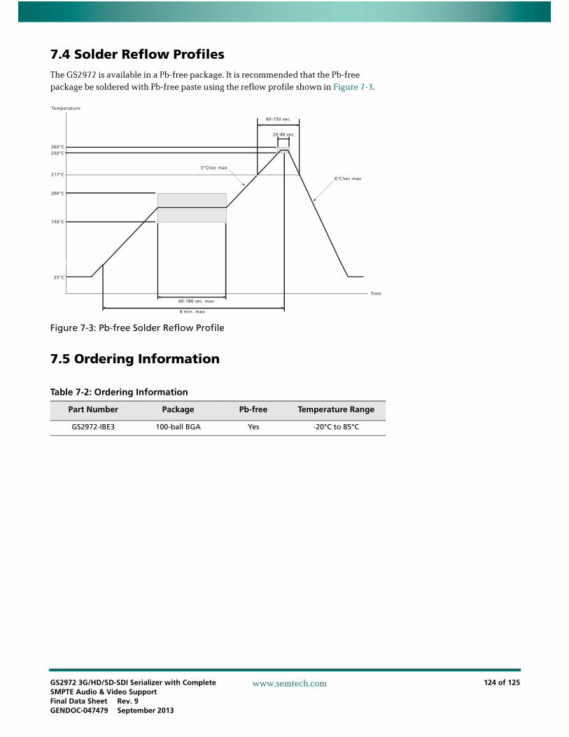
GS2972 3G/HD/SD-SDI Serializer with Complete SMPTE Audio & Video SupportFinal Data Sheet Rev. 9GENDOC-047479 September 2013
124 of 125
www.semtech.com
7.4 Solder Reflow ProfilesThe GS2972 is available in a Pb-free package. It is recommended that the Pb-free package be soldered with Pb-free paste using the reflow profile shown in Figure 7-3.
Figure 7-3: Pb-free Solder Reflow Profile
7.5 Ordering Information
25°C
150°C
200°C
217°C
260°C250°C
Time
Temperature
8 min. max
60-180 sec. max
60-150 sec.
20-40 sec.
3°C/sec max
6°C/sec max
Table 7-2: Ordering Information
Part Number Package Pb-free Temperature Range
GS2972-IBE3 100-ball BGA Yes -20°C to 85°C

© Semtech 2012
All rights reserved. Reproduction in whole or in part is prohibited without the prior written consent of the copyright owner. The information presented in this document does not form part of any quotation or contract, is believed to be accurate and reliable and may be changed without notice. No liability will be accepted by the publisher for any consequence of its use. Publication thereof does not convey nor imply any license under patent or other industrial or intellectual property rights. Semtech assumes no responsibility or liability whatsoever for any failure or unexpected operation resulting from misuse, neglect improper installation, repair or improper handling or unusual physical or electrical stress including, but not limited to, exposure to parameters beyond the specified maximum ratings or operation outside the specified range.
SEMTECH PRODUCTS ARE NOT DESIGNED, INTENDED, AUTHORIZED OR WARRANTED TO BE SUITABLE FOR USE IN LIFE-SUPPORT APPLICATIONS, DEVICES OR SYSTEMS OR OTHER CRITICAL APPLICATIONS. INCLUSION OF SEMTECH PRODUCTS IN SUCH APPLICATIONS IS UNDERSTOOD TO BE UNDERTAKEN SOLELY AT THE CUSTOMER’S OWN RISK. Should a customer purchase or use Semtech products for any such unauthorized application, the customer shall indemnify and hold Semtech and its officers, employees, subsidiaries, affiliates, and distributors harmless against all claims, costs damages and attorney fees which could arise.
Notice: All referenced brands, product names, service names and trademarks are the property of their respective owners.
DOCUMENT IDENTIFICATIONFINAL DATA SHEETInformation relating to this product and the application or design described herein is believed to be reliable, however such information is provided as a guide only and Semtech assumes no liability for any errors in this document, or for the application or design described herein. Semtech reserves the right to make changes to the product or this document at any time without notice.
GS2972 3G/HD/SD-SDI Serializer with Complete SMPTE Audio & Video SupportFinal Data Sheet Rev. 9GENDOC-047479 September 2013
125 of 125125
Contact Information
Semtech CorporationGennum Products Division
200 Flynn Road, Camarillo, CA 93012Phone: (805) 498-2111, Fax: (805) 498-3804
www.semtech.com
CAUTIONELECTROSTATIC SENSITIVE DEVICES
DO NOT OPEN PACKAGES OR HANDLE EXCEPT AT A STATIC-FREE WORKSTATION
www.semtech.com

Mouser Electronics
Authorized Distributor
Click to View Pricing, Inventory, Delivery & Lifecycle Information: Semtech:
GS2972-IBE3