GRT INSTITUTE OF ENGINEERING AND TECHNOLOGY, Tiruttani
77
GRT INSTITUTE OF ENGINEERING AND TECHNOLOGY, Tiruttani (Approved by AICTE, New Delhi, Affiliated to Anna University, Chennai) (An IS0 9001- 2008 certified Institution) GRT Mahalakshmi Nagar, Chennai-Tirupathi Highway, Tiruttani-631209, Tiruvallur Dt.TN -------------------------------------------------------------------------------------------------------- \ DEPARTMENT OE ELECTRONICS AND COMMUNICATION ENGINEERING Prepared by, Approved by, 1. S. NIJANDAN, AP/ECE Dr.P.SIVAKUMAR, HOD/ECE 2. U.SANDHYA, AP/ECE EC6412 – LINEAR INTEGRATED CIRCUITS LAB (Regulation 2013) Page 1 of 77 GRTIET
Transcript of GRT INSTITUTE OF ENGINEERING AND TECHNOLOGY, Tiruttani

GRT INSTITUTE OFENGINEERING ANDTECHNOLOGY, Tiruttani
(Approved by AICTE, New Delhi, Affiliated to Anna University, Chennai)(An IS0 9001- 2008 certified Institution)
GRT Mahalakshmi Nagar, Chennai-Tirupathi Highway, Tiruttani-631209, Tiruvallur Dt.TN
--------------------------------------------------------------------------------------------------------
\
DEPARTMENT OE ELECTRONICS ANDCOMMUNICATION ENGINEERING
Prepared by, Approved by,
1. S. NIJANDAN, AP/ECE Dr.P.SIVAKUMAR, HOD/ECE
2. U.SANDHYA, AP/ECE
EC6412 – LINEAR INTEGRATEDCIRCUITS LAB(Regulation 2013)
Page 1 of 77
GRTIET

LIST OF EXPERIMENTS
Design and Testing of
1. Inverting, Non – inverting and Differential amplifiers.
2. Integrator and Differentiator.
3. Instrumentation amplifier.
4. Active low pass and band pass filter.
5. Astable, monostable multivibrator and Schmitt trigger using Op – amp.
6. Wein bridge and RC Phase shift oscillator using Op – amp.
7. Astable and monostable multivibrator using NE 555 timer.
8. Frequency multiplier using PLL.
9. DC power supply using LM 317.
10.Study of SMPS
SIMULATION USING SPICE
11.Simulation of Experiments 3, 4, 5, 6 and 7 using PSpice netlists
12. Digital to analog converter (R – 2R ladder type)
13. Analog Multiplier
14. CMOS Inverter, NAND and NOR using PSPICE
CONTENT BEYOND SYLLABUS
1. Design and testing of summing amplifier
2. Design and testing of precision rectifier
Note: Op-Amps uA741, LM 301, LM311, LM 324 & AD 633 may be used
Page 2 of 77
GRTIET
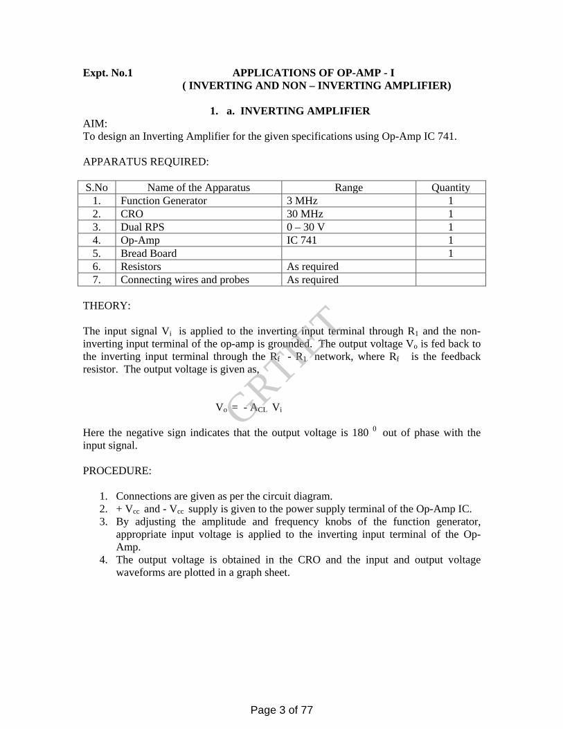
Expt. No.1 APPLICATIONS OF OP-AMP - I ( INVERTING AND NON – INVERTING AMPLIFIER)
1. a. INVERTING AMPLIFIER AIM: To design an Inverting Amplifier for the given specifications using Op-Amp IC 741. APPARATUS REQUIRED: S.No Name of the Apparatus Range Quantity
1. Function Generator 3 MHz 1 2. CRO 30 MHz 1 3. Dual RPS 0 – 30 V 1 4. Op-Amp IC 741 1 5. Bread Board 1 6. Resistors As required 7. Connecting wires and probes As required
THEORY: The input signal Vi is applied to the inverting input terminal through R1 and the non-inverting input terminal of the op-amp is grounded. The output voltage Vo is fed back to the inverting input terminal through the Rf - R1 network, where Rf is the feedback resistor. The output voltage is given as,
Vo = - ACL Vi
Here the negative sign indicates that the output voltage is 180 0 out of phase with the input signal. PROCEDURE:
1. Connections are given as per the circuit diagram. 2. + Vcc and - Vcc supply is given to the power supply terminal of the Op-Amp IC. 3. By adjusting the amplitude and frequency knobs of the function generator,
appropriate input voltage is applied to the inverting input terminal of the Op-Amp.
4. The output voltage is obtained in the CRO and the input and output voltage waveforms are plotted in a graph sheet.
Page 3 of 77
GRTIET

PIN DIAGRAM:
CIRCUIT DIAGRAM OF INVERTING AMPLIFIER:
DESIGN: We know for an inverting Amplifier ACL = RF / R1 Assume R1 ( approx. 10 KΩ ) and find Rf Hence Vo = - ACL Vi OBSERVATIONS:
S.No Input Output Practical Theoretical
1. Amplitude ( No. of div x Volts per div )
2. Time period ( No. of div x Time per div )
Page 4 of 77
GRTIET

MODEL GRAPH: RESULT: The design and testing of the inverting amplifier is done and the input and output waveforms were drawn.
1. b. NON - INVERTING AMPLIFIER AIM: To design a Non-Inverting Amplifier for the given specifications using Op-Amp IC 741. APPARATUS REQUIRED: S.No Name of the Apparatus Range Quantity
1. Function Generator 3 MHz 1 2. CRO 30 MHz 1 3. Dual RPS 0 – 30 V 1 4. Op-Amp IC 741 1 5. Bread Board 1 6. Resistors As required 7. Connecting wires and probes As required
THEORY: The input signal Vi is applied to the non - inverting input terminal of the op-amp. This circuit amplifies the signal without inverting the input signal. It is also called negative feedback system since the output is feedback to the inverting input terminals. The differential voltage Vd at the inverting input terminal of the op-amp is zero ideally and the output voltage is given as,
Vo = ACL Vi
Page 5 of 77
GRTIET

Here the output voltage is in phase with the input signal. PROCEDURE:
1. Connections are given as per the circuit diagram. 2. + Vcc and - Vcc supply is given to the power supply terminal of the Op-Amp IC. 3. By adjusting the amplitude and frequency knobs of the function generator,
appropriate input voltage is applied to the non - inverting input terminal of the Op-Amp.
4. The output voltage is obtained in the CRO and the input and output voltage waveforms are plotted in a graph sheet.
PIN DIAGRAM:
CIRCUIT DIAGRAM OF NON INVERITNG AMPLIFIER:
Page 6 of 77
GRTIET
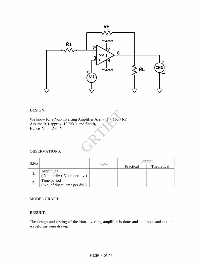
DESIGN: We know for a Non-inverting Amplifier ACL = 1 + ( RF / R1) Assume R1 ( approx. 10 KΩ ) and find Rf Hence Vo = ACL Vi OBSERVATIONS:
S.No Input Output Practical Theoretical
1. Amplitude ( No. of div x Volts per div )
2. Time period ( No. of div x Time per div )
MODEL GRAPH: RESULT: The design and testing of the Non-inverting amplifier is done and the input and output waveforms were drawn.
Page 7 of 77
GRTIET

Expt. No.2 APPLICATIONS OF OP-AMP - II (DIFFERENTIATOR AND INTEGRATOR)
2. a. DIFFERENTIATOR
AIM: To design a Differentiator circuit for the given specifications using Op-Amp IC 741. APPARATUS REQUIRED: S.No Name of the Apparatus Range Quantity
1. Function Generator 3 MHz 1 2. CRO 30 MHz 1 3. Dual RPS 0 – 30 V 1 4. Op-Amp IC 741 1 5. Bread Board 1 6. Resistors 7. Capacitors 8. Connecting wires and probes As required
THEORY: The differentiator circuit performs the mathematical operation of differentiation; that is, the output waveform is the derivative of the input waveform. The differentiator may be constructed from a basic inverting amplifier if an input resistor R1 is replaced by a capacitor C1 . The expression for the output voltage is given as,
Vo = - Rf C1 ( dVi /dt ) Here the negative sign indicates that the output voltage is 180 0 out of phase with the input signal. A resistor Rcomp = Rf is normally connected to the non-inverting input terminal of the op-amp to compensate for the input bias current. A workable differentiator can be designed by implementing the following steps:
1. Select fa equal to the highest frequency of the input signal to be differentiated. Then, assuming a value of C1 < 1 µF, calculate the value of Rf.
2. Choose fb = 20 fa and calculate the values of R1 and Cf so that R1C1 = Rf Cf.
The differentiator is most commonly used in waveshaping circuits to detect high frequency components in an input signal and also as a rate–of–change detector in FM modulators.
Page 8 of 77
GRTIET

PIN DIAGRAM:
CIRCUIT DIAGRAM OF DIFFERENTIATOR:
DESIGN : [ To design a differentiator circuit to differentiate an input signal that varies in frequency from 10 Hz to about 1 KHz. If a sine wave of 1 V peak at 1000Hz is applied to the differentiator , draw its output waveform.] Given fa = 1 KHz We know the frequency at which the gain is 0 dB, fa = 1 / (2π Rf C1) Let us assume C1 = 0.1 µF ; then
Page 9 of 77
GRTIET

Rf = _________ Since fb = 20 fa , fb = 20 KHz We know that the gain limiting frequency fb = 1 / (2π R1 C1) Hence R1 = _________ Also since R1C1 = Rf Cf ; Cf = _________ Given Vp = 1 V and f = 1000 Hz, the input voltage is Vi = Vp sin ωt We know ω = 2πf Hence Vo = - Rf C1 ( dVi /dt ) = - 0.94 cos ωt PROCEDURE:
1. Connections are given as per the circuit diagram. 2. + Vcc and - Vcc supply is given to the power supply terminal of the Op-Amp IC. 3. By adjusting the amplitude and frequency knobs of the function generator,
appropriate input voltage is applied to the inverting input terminal of the Op-Amp.
4. The output voltage is obtained in the CRO and the input and output voltage waveforms are plotted in a graph sheet.
OBSERVATIONS:
S.No Input Output
1. Amplitude ( No. of div x Volts per div )
2. Time period ( No. of div x Time per div )
2. b. INTEGRATOR
AIM: To design an Integrator circuit for the given specifications using Op-Amp IC 741. APPARATUS REQUIRED: S.No Name of the Apparatus Range Quantity
1. Function Generator 3 MHz 1 2. CRO 30 MHz 1 3. Dual RPS 0 – 30 V 1 4. Op-Amp IC 741 1
Page 10 of 77
GRTIET

5. Bread Board 1 6. Resistors 7. Capacitors 8. Connecting wires and probes As required
THEORY: A circuit in which the output voltage waveform is the integral of the input voltage waveform is the integrator. Such a circuit is obtained by using a basic inverting amplifier configuration if the feedback resistor Rf is replaced by a capacitor Cf . The expression for the output voltage is given as,
Vo = - (1/Rf C1 ) ∫ Vi dt Here the negative sign indicates that the output voltage is 180 0 out of phase with the input signal. Normally between fa and fb the circuit acts as an integrator. Generally, the value of fa < fb . The input signal will be integrated properly if the Time period T of the signal is larger than or equal to Rf Cf . That is,
T ≥ Rf Cf
The integrator is most commonly used in analog computers and ADC and signal-wave shaping circuits. PIN DIAGRAM:
CIRCUIT DIAGRAM OF INTEGRATOR:
Page 11 of 77
GRTIET

DESIGN: [ To obtain the output of an Integrator circuit with component values R1Cf = 0.1ms , Rf = 10 R1 and Cf = 0.01 µF and also if 1 V peak square wave at 1000Hz is applied as input.] We know the frequency at which the gain is 0 dB, fb = 1 / (2π R1 Cf) Therefore fb = _____ Since fb = 10 fa , and also the gain limiting frequency fa = 1 / (2π Rf Cf) We get , R1 = _______ and hence Rf = __________ PROCEDURE:
1. Connections are given as per the circuit diagram. 2. + Vcc and - Vcc supply is given to the power supply terminal of the Op-Amp IC. 3. By adjusting the amplitude and frequency knobs of the function generator,
appropriate input voltage is applied to the inverting input terminal of the Op-Amp.
4. The output voltage is obtained in the CRO and the input and output voltage waveforms are plotted in a graph sheet.
OBSERVATIONS:
S.No Input Output
1. Amplitude ( No. of div x Volts per div )
2. Time period ( No. of div x Time per div )
Page 12 of 77
GRTIET
CIRCUIT DIAGRAM: INTEGRATOR Cf= 0.01µF R1=15KΩ
+Vcc=12V
2 7 - 6 Vo
3 + IC741
4 Vi -Vee=-12V
Rcomp 15KΩ
DIFFERENTIATOR Rf = 15KΩ
C1 = 0.01µF +Vcc=12V
2 7 -
6 Vo 3 IC741
+
Vi 4 -Vee=-12V
Rcomp 15KΩ
CRO
CRO
Page 13 of 77
GRTIET

MODEL GRAPH: DIFFERENTIATOR Vi t (msec) Vo t(msec)
MODEL GRAPH: INTEGRATOR Vi t (msec) Vo t(msec) RESULT:- Thus the integrator and differentiator using op-amp is studied.
Page 14 of 77
GRTIET

3. SECOND ORDER ACTIVE LOW PASS FILTER
AIM: Design a second order active Butterworth low pass filter having upper cut off
frequency 1 KHz, also determine its frequency response using IC 741. APPARATUS REQUIRED :
S.NO ITEM RANGE Q.TY
1 OP-AMP IC741 1 2 RESISTOR 10KΩ,
1.5KΩ 5.6 KΩ
1 1 1
3 Capacitor 0.1 µF 1 4 CRO - 1 5 RPS DUAL(0-30) V 1
DESIGN: Given: fH = 1 KHz = 1/ (2πRC) Let C = 0.1 µF, R = 1.6 KΩ For n = 2, α (damping factor) = 1.414, Passband gain = Ao = 3 - α =3 – 1.414 = 1.586. Transfer function of second order butterworth LPF as: 1.586 H(s) = --------------------------- S2 + 1.414 s + 1 Now Ao = 1 + (Rf / R1) = 1.586 = 1 + 0.586 Let Ri = 10 KΩ, then Rf = 5.86 KΩ
Page 15 of 77
GRTIET

CIRCUIT DIAGRAM: Ri = 10 KΩ Rf = 5.86 KΩ +Vcc=+12 V R = 1.6 KΩ R = 1.6 KΩ 2 7 - IC Vo 3 + 741 6 4 -Vcc= - 12 V C = 0.1 µF C = 0.1 µF
Frequency Response Characteristics: (Use Semi – log Graph):
Gain - 3 dB In dB fc = 1KHz Frequency (Hz)
Page 16 of 77
GRTIET

THEORY: An improved filter response can be obtained by using a second order active filter. A second order filter consists of two RC pairs and has a roll-off rate of -40 dB/decade. A general second order filter (Sallen Kay filter) is used to analyze different LP, HP, BP and BSF. PROCEDURE : The connections are made as shown in the circuit diagram. The signal which has to be made sine is applied to the RC filter pair circuit with the non-inverting terminal. The supply voltage is switched ON and the o/p voltages are recorded through CRO by varying different frequencies from 10 Hz to 100 KHz and tabulate the readings. Calculating Gain through the formula and plotting the frequency response characteristics using Semi-log graph sheet and finding out the 3 dB line for fc.
OBSERVATION:
VIN = 1 Volt
S.No.
FREQUNCY Hz
O/P voltage VO Volts
Av=20 log Vo/Vi dB
RESULT:
Thus the second order Active Low Pass filter is designed and its frequency
response characteristic curves are drawn.
Page 17 of 77
GRTIET

4. SQUARE WAVE GENERATOR AIM: To design a square wave generator circuit for the frequency of Oscillations of 1KHZ APPARATUS REQUIRED : S.NO ITEM RANGE Q.TY
1 OP-AMP IC741 1 2 RESISTOR 4.7KΩ,
1KΩ 1.16KΩ
1 1 1
3 CAPACITOR 0.1µF 1 4 CRO - 1 5 RPS DUAL(0-30) V 1
DESIGN: F=1KHZ =T=1ms R2=1KΩ,C=0.1µF R1=1.16R2=1.16KΩ≅1KΩ+100Ω T=2RC R=T/2C =5KΩ ≅4.7KΩ THEORY: A simple op-Amp square wave generator is also called as free running oscillator, the principle of generation of square wave output is to force an op-amp to operate in the saturation region . A fraction β=R2/(R1+R2) of the output is fed back to the (+) input terminal. The output is also fed to the (-) terminal after integrating by means of a low pass Rc combination in astable multivibrator both the states are quasistables. the frequency is determined by the time taken by the capacitor to charge from- βVsat to+βVsat.
Page 18 of 77
GRTIET

CIRCUIT DIAGRAM:
4.7 KΩ +Vcc= +12 V 2 7 IC Vo 3 741 6 4 -Vcc = - 12 V 1.16 KΩ 0.1µF
1KΩ
MODEL GRAPH: + Vcc
+Vsat + βVsat - βVsat -Vsat - Vee
Page 19 of 77
GRTIET

Pin Diagram:
Offset Null 1 8 No connection Inverting 2 IC 741 7 +Vcc Non-Inverting 3 6 Output -Vee 4 5 Offset Null
PROCEDURE: 1.The connection is given as per the circuit diagram. 2.connect the CRO in the output and trace the square waveform. 3.calculate the practical frequency and compare with the theoretical Frequency. 4.plot the waveform obtained and mark the frequency and time period. RESULT: Thus the square waveforms are generated using square wave generator Theoretical frequency= Practical frequency=
Page 20 of 77
GRTIET
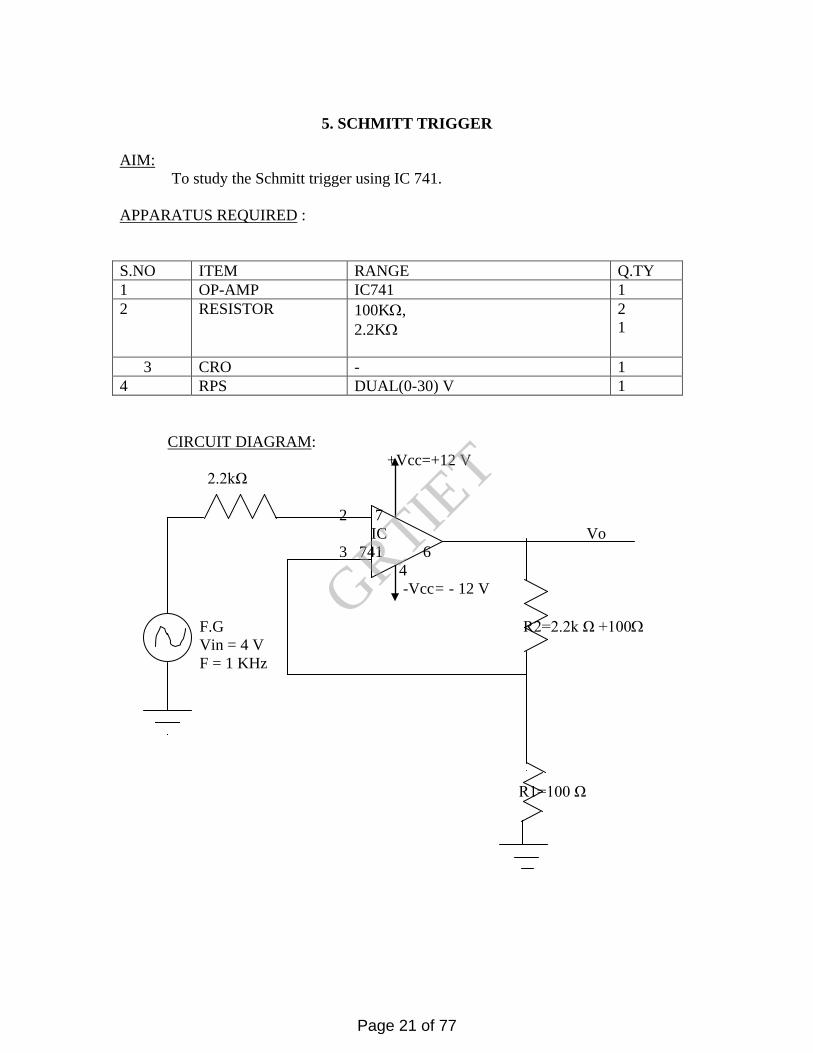
5. SCHMITT TRIGGER
AIM:
To study the Schmitt trigger using IC 741. APPARATUS REQUIRED :
S.NO ITEM RANGE Q.TY 1 OP-AMP IC741 1 2 RESISTOR 100KΩ,
2.2KΩ
2 1
3 CRO - 1 4 RPS DUAL(0-30) V 1
CIRCUIT DIAGRAM: +Vcc=+12 V 2.2kΩ 2 7 IC Vo 3 741 6 4 -Vcc= - 12 V F.G R2=2.2k Ω +100Ω Vin = 4 V F = 1 KHz
R1=100 Ω
Page 21 of 77
GRTIET

Pin Diagram:
Offset Null 1 8 No connection Inverting 2 IC 741 7 +Vcc Non-Inverting 3 6 Output -Vee 4 5 Offset Null O/P wave form: Vo (v) t THEORY: Schmitt trigger is useful in squaring of slowly varying i/p waveforms.Vin is applied to inverting terminal of op-amp .Feedback voltage is applied to the non-inverting terminal. LTP is the point at which output changes from high level to low level .This is highly useful in triangular waveform generation, wave shape pulse generator, A/D convertor etc. PROCEDURE : The connections are made as shown in the circuit diagram.The signal which has to be made square is applied to the inverting terminal . Here the i/p is a sine waveform.The supply voltage is switched ON and the o/p waveform is recorded through CRO.The UTP and LTP are also found and the theoretical and practical values are verified. LTP = R1/ ( R1 + R2 ) X(-Vsat) UTP = R2 /( R1 + R2 ) X( +Vsat)
Design : +Vsat= +Vcc=15v -Vsat= -Vee= -15v RESULT:The Schmitt trigger circuit is connected and the waveforms are drawn and theoretical and practical values for the trip points are verified. Theoretical values =
Practical values =
Page 22 of 77
GRTIET
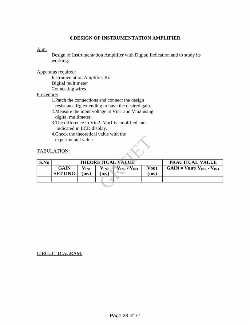
6.DESIGN OF INSTRUMENTATION AMPLIFIER
Aim:
Design of Instrumentation Amplifier with Digital Indication and to study its working.
Apparatus required: Instrumentation Amplifier Kit Digital multimeter Connecting wires
Procedure: 1.Patch the connections and connect the design resistance Rg extending to have the desired gain. 2.Measure the input voltage at Vin1 and Vin2 using digital multimeter. 3.The difference in Vin2- Vin1 is amplified and indicated in LCD display. 4.Check the theoretical value with the experimental value.
TABULATION:
S.No THEORETICAL VALUE PRACTICAL VALUE GAIN
SETTING VIN1 (mv)
VIN2 (mv)
VIN2 - VIN1 Vout (mv)
GAIN = Vout/ VIN2 - VIN1
CIRCUIT DIAGRAM:
Page 23 of 77
GRTIET

0
A1
1 2
A2
1 2
A3
1 2
R1
R2
R5
R4
R7
R6
R5
Result:
Thus the instrumentation amplifier with digital indication was designed and the working of this was studied.
Page 24 of 77
GRTIET

7.RC PHASE SHIFT OSCILLATOR AIM: To construct a RC phase shift oscillator to generate sine wave using op-amp.
APPARATUS REQUIRED: S.NO ITEM RANGE Q.TY 1 OP-AMP IC-741 1 2 RESISTOR 16KΩ, 32KΩ,
1.59KΩ, 1 2
3 CAPACITOR 0.1µf
2
4 CRO - 1 5 RPS DUAL(0-30) V 1 THEORY: Basically,positive feedback of a fraction of output voltage of a amplifier fed to the input in the same phase, generate sine wave. The op-amp provides a phase shift of 180 degree as it is used in the inverting mode.An additional phase shift of 180 degree is provided by the feedback Rc network.The frequency of the oscillator fo is given by fo = 1 / √ 6 (2 π R C ) Also the gain of the inverting op-amp ahould be atleast 29,or Rf ≥ 29 R1
Page 25 of 77
GRTIET

RC PHASE SHIFT OSCILLATOR
Design: fo = 1 / √ 6 (2 π R C )
Rf ≥ 29 R1 C = 0.01µF, fo = 500 Hz.
R = 1 / √ 6 (2 π f C ) = 13 k Therefore, Choose R = 15k To prevent loading, R1 ≥ 10 R R1 =10 R = 150 k. Rf = 4.35 M
CRO
R1=150k
Rf =470k
741
R = 1.5 k
C =0.01µF
2
3
Page 26 of 77
GRTIET

MODEL GRAPH:
Observations: Time period =
Frequency =
Amplitude =
Procedure:
1. Connect the circuit as shown in fig. With the design values.
2. Observe the output waveforms using a CRO.For obtaining sine wave adjust Rf.
3. Measure the output wave frequency and amplitude.
Result:
The sine wave output signal is obtained in RC phase shift oscillator.
Frequency f =
t
T
Page 27 of 77
GRTIET

8. WEIN BRIDGE OSCILLATOR
AIM: To construct a wein bridge oscillator for fo = I khz and study its operation
APPARATUS REQUIRED: S.NO ITEM RANGE Q.TY 1 OP-AMP IC-741 1 2 RESISTOR 16KΩ, 32KΩ,
1.59KΩ, 1 2
3 CAPACITOR 0.1µf
2
4 CRO - 1 5 RPS DUAL(0-30) V 1 THEORY: In wein bridge oscillator ,wein bridge circuit is connected between the amplifier input terminals and output terminals . The bridge has a series rc network in one arm and parallel network in the adjoining arm. In the remaining 2 arms of the bridge resistors R1and Rf are connected . To maintain oscillations total phase shift around the circuit must be zero and loop gain unity. First condition occurs only when the bridge is p balanced . Assuming that the resistors and capacitors are equal in value ,the resonant frequency of balanced bridge is given by Fo = 0.159 / RC Design :
At the frequency the gain required for sustained oscillations is given by 1+Rf /R1 = 3 or Rf = 2R1 Fo = 0.65/RC and Rf = 2R1 Calculation: Theoretical Fr = 1/(2*3.14*R*C)
Page 28 of 77
GRTIET

CIRCUITDIAGRAM
Calculation: Theoretical: F = 1/(2*3.14*R*C) Practical: F = 1/T
Page 29 of 77
GRTIET

PROCEDURE: Connections are made as per the diagram .R,C,R1,Rf are calculated for the given value of Fo using the design . Output waveform is traced in the CRO . RESULT : Hence the wein bridge oscillator is studied and its output waveform traced.
Page 30 of 77
GRTIET
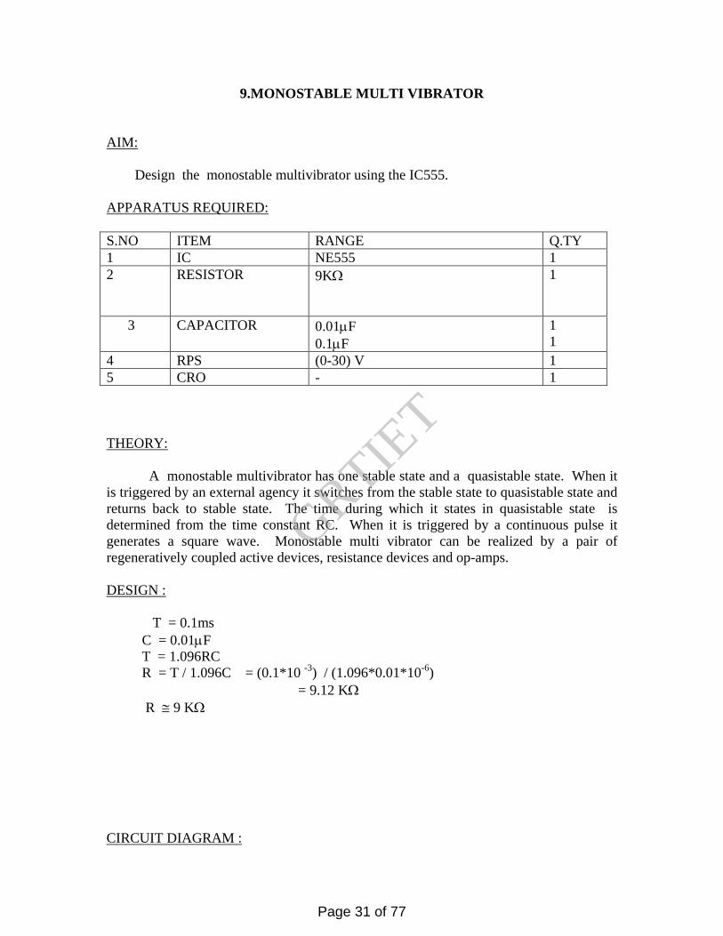
9.MONOSTABLE MULTI VIBRATOR AIM: Design the monostable multivibrator using the IC555. APPARATUS REQUIRED:
S.NO ITEM RANGE Q.TY 1 IC NE555 1 2 RESISTOR 9KΩ
1
3 CAPACITOR 0.01µF 0.1µF
1 1
4 RPS (0-30) V 1 5 CRO - 1
THEORY: A monostable multivibrator has one stable state and a quasistable state. When it is triggered by an external agency it switches from the stable state to quasistable state and returns back to stable state. The time during which it states in quasistable state is determined from the time constant RC. When it is triggered by a continuous pulse it generates a square wave. Monostable multi vibrator can be realized by a pair of regeneratively coupled active devices, resistance devices and op-amps. DESIGN : T = 0.1ms C = 0.01µF T = 1.096RC R = T / 1.096C = (0.1*10 -3) / (1.096*0.01*10-6)
= 9.12 KΩ R ≅ 9 KΩ CIRCUIT DIAGRAM :
Page 31 of 77
GRTIET

PINDIAGRAM: PROCEDURE: The connections are made as per the diagram. The value of R is chosen as 9kΩ. The DCB is set to the designed value. The power supply is switched on and set to +5V. The output of the pulse generator is set to the desired frequency. Here the frequency of triggering should be greater than width of ON period (i.e.) T >W. The output is observed using CRO and the result is compared with the theoretical value. The experiment can be repeated for different values of C and the results are tabulated.
OBSERVATION C (uf)
Theoritical(T=1.095 RC(ms)))
Practical T(ms)
Page 32 of 77
GRTIET

RESULT: Thus the monostable multivibrator using IC555 is designed and its output waveform is traced
Page 33 of 77
GRTIET

10.ASTABLE MULTIVIBRATOR
Aim: To study the application of IC555 as an astable multivibrator. APPARATUS REQUIRED : S.NO ITEM RANGE Q.TY
1 IC NE555 1 2 RESISTOR 1KΩ,
2.2KΩ
1 1
3 CAPACITOR
0.1µF 0.01µF
1 1
4 CRO - 1 5 RPS DUAL(0-30) V 1
Theory: The IC555 timer is a 8 pin IC that can be connected to external components for astable operation. The simplified block diagram is drawn. The OP-AMP has threshold and control inputs. Whenever the threshold voltage exceeds the control voltage, the high output from the OP –AMP will set the flip-flop. The collector of discharge transistor goes to pin 7. When this pin is connected to an external trimming capacitor, a high Q output from the flip flop will saturate the transistor and discharge the capacitor. When Q is low the transistor opens and the capacitor charges.
The complementary signal out of the flip-flop goes to pin 3 and output. When external reset pin is grounded it inhibits the device. The on – off feature is useful in many application. The lower OP- AMP inverting terminal input is called the trigger because of the voltage divider. The non-inverting input has a voltage of +Vcc/3, the OP-Amp output goes high and resets the flip flop.
Circuit diagram:
Page 34 of 77
GRTIET

PIN DIAGRAM:
Procedure : The connections are made as per the circuit diagram and the values of R and C are calculated assuming anyone term and they are settled . The output waveform is noted down and graph is drawn and also the theoretical and practical time period is verified.
Observation:
Page 35 of 77
GRTIET
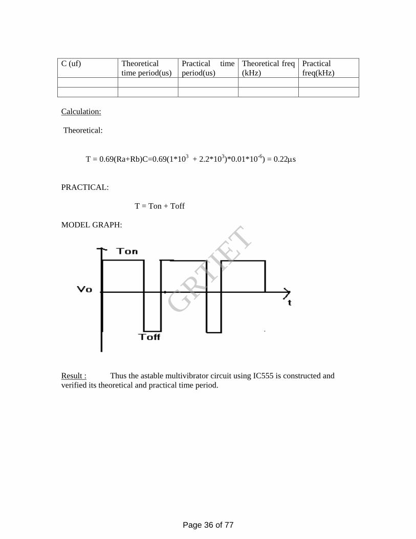
C (uf) Theoretical
time period(us) Practical time period(us)
Theoretical freq (kHz)
Practical freq(kHz)
Calculation: Theoretical:
T = 0.69(Ra+Rb)C=0.69(1*103 + 2.2*103)*0.01*10-6) = 0.22µs
PRACTICAL:
T = Ton + Toff MODEL GRAPH:
Result : Thus the astable multivibrator circuit using IC555 is constructed and verified its theoretical and practical time period.
Page 36 of 77
GRTIET

11. PLL CHARACTERISTICS
Aim:
To construct and study the operation of PLL IC 565 and determine its Characteristics.
Apparatus Required: S.No Components
Range Quantity 1 IC 565 - 1 2 Resistors 6.8 KΩ 1 3 Capacitors 0.001 µF
0.1 µF, 1 µF 1 each
4 FunctionGenerator (Digital) 1 Hz – 2 MHz 1 5 C.R.O - 1 6 Dual Power Supply 0- 30 V 1 Circuit Diagram:
+ 6 V R1 6.8 KΩ C = 1 µF C1 = 0.01 µF Demodulated O/p Reference O/p VCO O/p (fO) Function Generator (Square Wave) Vi Input CT = 0.001 µF - 6 V
Pin Diagram (IC 565 - PLL)
10 8 7 2 6 3 IC 565 4 9 1 5
Page 37 of 77
GRTIET

+ VCC 1 14 NC Input 2 13 NC Output 3 12 NC
IC 565 VCO I/P 4 11 NC VCO O/P 5 10 + VCC Output 6 9 VCO CT
Demodulated 7 8 VCO RT Output Procedure:
1. The connections are given as per the circuit diagram. 2. Measure the free running frequency of VCO at pin 4, with the input signal Vi set
equal to zero. Compare it with the calculated value = 0.25 / (RT CT). 3. Now apply the input signal of 1 VPP square wave at a 1 KHz to pin 2. Connect
one channel of the scope to pin 2 and display this signal on the scope.
4. Gradually increase the input frequency till the PLL is locked to the input frequency.This frequency f1 gives the lower end of the capture range.Go on increasing the input frequency, till Pll tracks the input signal,say ,to a frequency f2.This frequency f2 gives the upper end of the lock range.If input frequency is increased further, the loop will get unlocked.
5. Now gradually decrease the input frequency till the Pll is again locked.This is the
frequency f3,the upper end of the capture range.Keep on decreasing the input frequency until the loop is unlocked.This frequency f4 gives the lower end of the lock range.
6. The lock range ∆fL = (f2 – f4).Compare it with the calculated value
of ± 7.8 fo / 12 .Also the capture range is ∆fc = (f3 – f1).Compare it with the calculated value of capture range. ∆fc = ± (∆fL / (2π)(3.6)(103) C)1/2
Model Graph
Page 38 of 77
GRTIET

vc Slope =1/Kv fo- ∆fL fo- ∆fc fo fo+ ∆fc fo+∆fL IB 2∆fc= Capture range 2∆fL = Lock- in range
Result :
Thus the PLL circuit is constructed and its Characteristics is determined.
Page 39 of 77
GRTIET

12. FREQUENCY MULTIPLIER USING PLL Aim:
To construct and study the operation of frequency multiplier using IC 565. Apparatus Required: S.No Components
Range Quantity 1 IC 565,IC 7490,2N2222 - 1 2 Resistors 20 KΩ, 2kΩ,
4.7kΩ,10kΩ 1
3 Capacitors 0.001 µF 10 µF
1 each
4 FunctionGenerator (Digital) 1 Hz – 2 MHz 1 5 C.R.O - 1 6 Dual Power Supply 0- 30 V 1 7. Circuit Diagram:
1
23
1 9
5
4
7810
2
3
2kohm
20kohm
+6v
10Mf
+6v
11
2 3 6 7 101
1
2N222210kohm
4.7kohm
-6v
0.01Mf
vin
VCO Output
Fo=5fin
565
7490(%5)
RT
RT
RT
C1
0.001Mf
C
Page 40 of 77
GRTIET

Procedure:
1. The connections are given as per the circuit diagram. 2. The circuit uses a 4- bit binary counter 7490 used as a divide-by-5 circuit. 3. Measure the free running frequency of VCO at pin 4, with the input signal Vi set
equal to zero. Compare it with the calculated value = 0.25 / (RT CT). 4. Now apply the input signal of 1 VPP square wave at 500 Hz to pin 2. 5. Vary the VCO frequency by adjusting the 20kΩ potentiometer till the PLL is
locked.Measure the output frequency.It should be 5 times the input frequency. 6. Repeat steps 4,5 for input frequency of 1 kHz and 1.5 kHz.
Result :
Thus the frequency multiplier circuit using PLL is constructed and studied.
Page 41 of 77
GRTIET
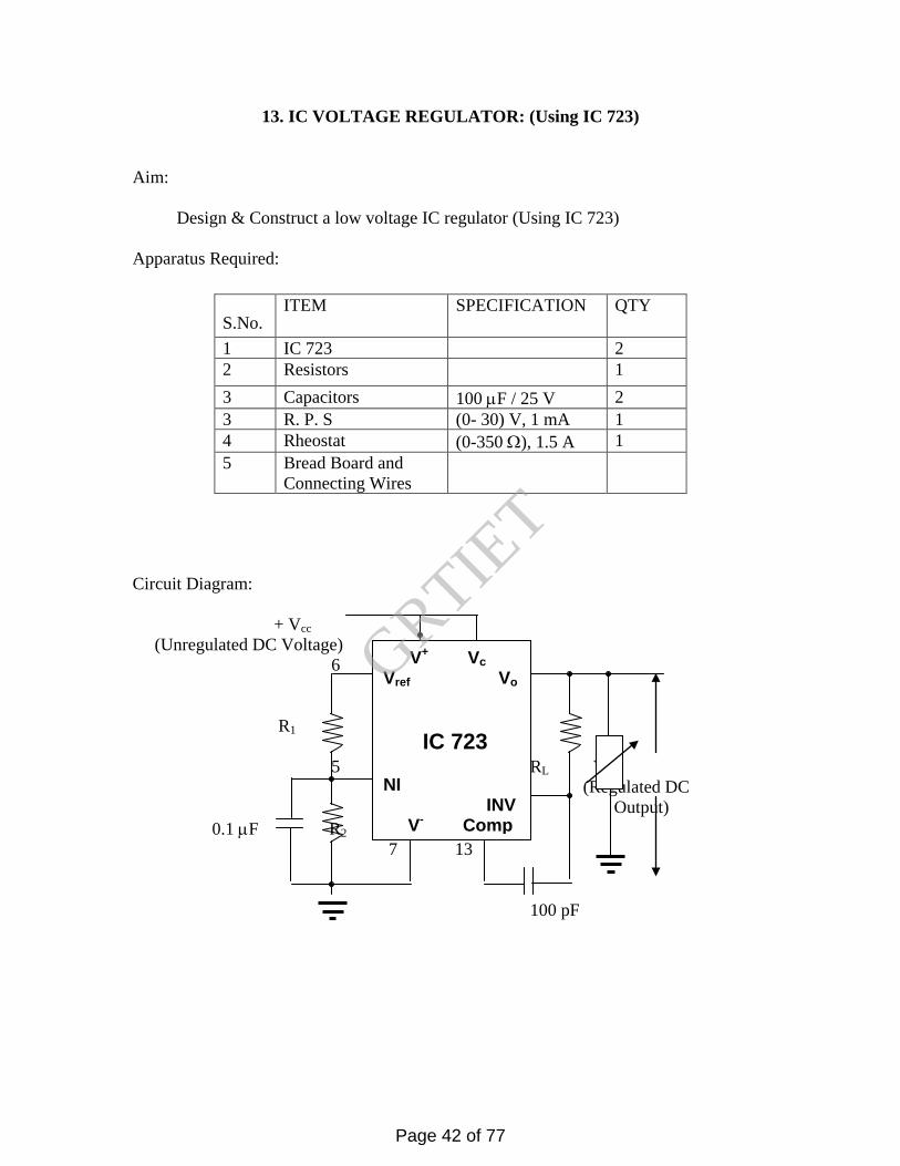
13. IC VOLTAGE REGULATOR: (Using IC 723) Aim: Design & Construct a low voltage IC regulator (Using IC 723) Apparatus Required: Circuit Diagram: + Vcc (Unregulated DC Voltage) 6 R1 R3 5 RL Vout 4 (Regulated DC Output) 0.1 µF R2 7 13 100 pF
S.No. ITEM SPECIFICATION QTY
1 IC 723 2 2 Resistors 1 3 Capacitors 100 µF / 25 V 2 3 R. P. S (0- 30) V, 1 mA 1 4 Rheostat (0-350 Ω), 1.5 A 1 5 Bread Board and
Connecting Wires
V+ Vc Vref Vo IC 723 NI INV V- Comp
Page 42 of 77
GRTIET
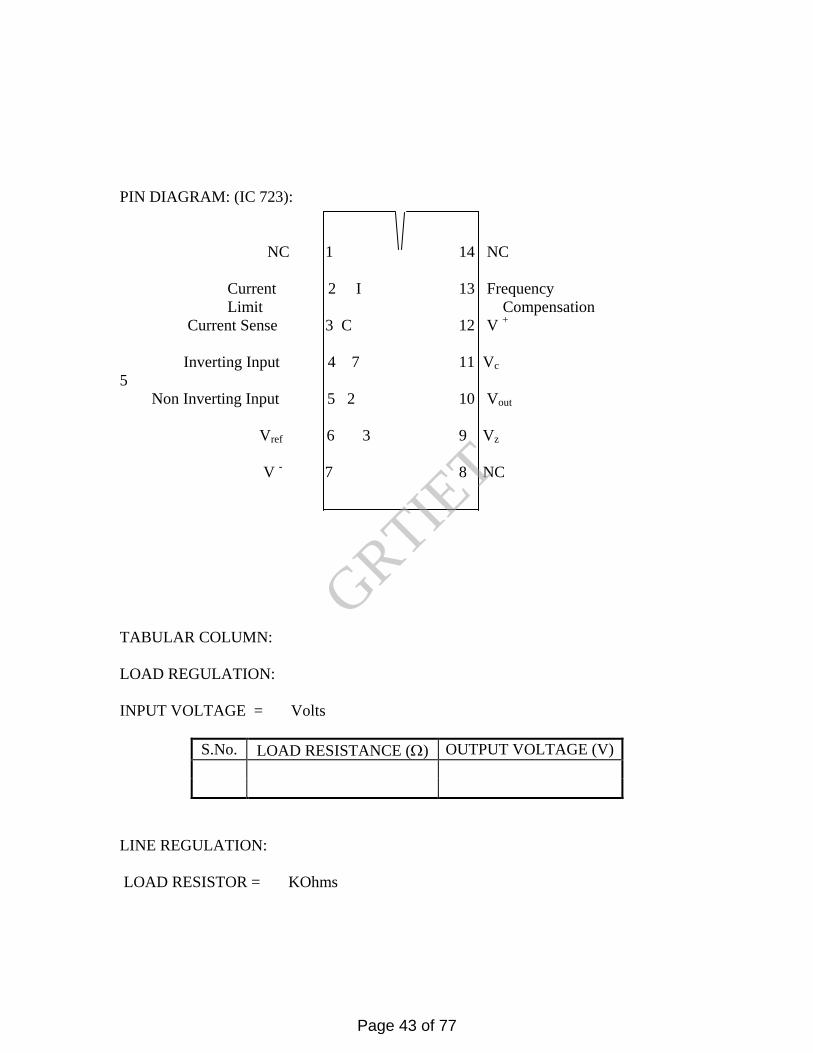
PIN DIAGRAM: (IC 723):
NC 1 14 NC Current 2 I 13 Frequency Limit Compensation Current Sense 3 C 12 V +
Inverting Input 4 7 11 Vc 5 Non Inverting Input 5 2 10 Vout Vref 6 3 9 Vz V - 7 8 NC TABULAR COLUMN: LOAD REGULATION: INPUT VOLTAGE = Volts
S.No. LOAD RESISTANCE (Ω) OUTPUT VOLTAGE (V)
LINE REGULATION: LOAD RESISTOR = KOhms
Page 43 of 77
GRTIET

S.No. INPUT VOLTAGE (V) OUTPUT VOLTAGE (V)
RESULT: The low voltage IC regulator is constructed and the regulation characteristics are tabulated and drawn its characteristics.
Page 44 of 77
GRTIET

EXP.NO: 10 DATE:
AIM:
To study the control of SMPS
THEORY:
The switching regulator is also called as switched mode regulator. In
this case, the pass transistor is used as a controlled switch and is operated at either
cutoff or saturated state. Hence the power transmitted across the pass device is in
discrete pulses rather than as a steady current flow. Greater efficiency is achieved
since the pass device is operated as a low impedance switch. When the pass device is
at cutoff, there is no current and dissipated power. Again when the pass device is in
saturation, a negligible voltage drop appears across it and thus dissipates only a small
amount of average power, providing maximum current to the load. The efficiency is
switched mode power supply is in the range of 70-90%.
A switching power supply is shown in figure. The bridge rectifier and
capacitor filters are connected directly to the ac line to give unregulated dc input. The
reference regulator is a series pass regulator. Its output serves as a power supply
voltage for all other circuits. The transistors Q1, Q2 are alternatively switched „on‟ &;
off, these transistors are either fully „on‟ or „cut-off, so they dissipate very little
power. These transistors drive the primary of the main transformer. The secondary is
centre tapped and full wave rectification is achieved by diodes D1 and D2. This
unidirectional square wave is next filtered through a two stage LC filter to produce
output voltage Vo.
SG 3524:
FUNCTION:
Switched Mode Power Supply Control Circuit
FEATURES:
Complete PWM Power Controlled circuitry.
Single ended or push-pull outputs.
Line and Load regulation of 0.2%.
1% maximum temperature variation.
Total Supply current is less than 10mA
Operation beyond 100KHz
RESULT:
Thus the control of SMPS IC SG3524 had been studied.
STUDY OF SMPS
Page 45 of 77
GRTIET

Instrumentation Amplifier:
Page 46 of 77
GRTIET

Program:
.LIB EVAL.LIB
VCC1 4 0 DC 15
VEE1 0 5 DC 15
VCC2 9 0 DC 15
VEE2 0 10 DC 15
VCC3 14 0 DC 15
VEE3 0 15 DC 15
V1 7 0 SIN(0 5V 100)
V2 1 0 SIN(0 3V 100)
R1 3 2 1K
R2 8 6 1K
R3 2 6 500
R4 3 11 1K
R5 8 12 1K
RF 11 13 1K
R6 12 0 1K
X1 1 2 4 5 3 UA741
X2 7 6 9 10 8 UA741
X3 12 11 14 15 13 UA741
.TRAN 0 20MS
.OP
.PROBE
.END
Page 47 of 77
GRTIET

Lowpass Filter:
Page 48 of 77
GRTIET

Program:
.LIB EVAL.LIB
VCC 5 0 DC 15
VEE 0 6 DC 15
VIN 2 0 AC 4
R1 1 0 22K
R2 1 4 22K
R3 2 3 1.5K
RL 4 0 10K
C1 3 0 0.1U
X1 3 1 5 6 4 UA741
.AC DEC 10 10 1MEG
.OP
.PROBE
.END
Page 49 of 77
GRTIET

Highpass Filter:
Page 50 of 77
GRTIET
Program:
.LIB EVAL.LIB
VCC 5 0 DC 15
VEE 0 6 DC 15
VIN 2 0 AC 4
R1 1 0 22K
R2 1 4 22K
C1 2 3 0.1U
RL 4 0 10K
R3 3 0 1.5K
X1 3 1 5 6 4 UA741
.AC DEC 10 10 100K
.OP
.PROBE
.END
Page 51 of 77
GRTIET
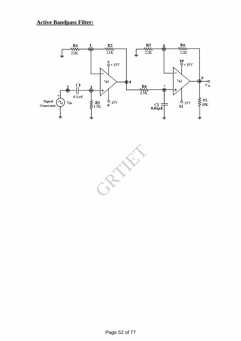
Active Bandpass Filter:
Page 52 of 77
GRTIET

Program:
.LIB EVAL.LIB
VCC 5 0 DC 15
VEE 0 6 DC 15
VCC1 10 0 DC 15
VEE1 0 11 DC 15
VIN 2 0 AC 4
R1 1 0 22K
R2 1 4 22K
R3 3 0 1.5K
R4 4 7 1.5K
R5 8 0 22K
R6 8 9 22K
RL 9 0 10K
C1 2 3 0.1U
C2 7 0 0.01U
X1 3 1 5 6 4 UA741
X2 7 8 10 11 9 UA741
.AC DEC 10 10 10MEG
.OP
.PROBE
.END
Page 53 of 77
GRTIET

Astable Multivibrator:
Page 54 of 77
GRTIET

Program:
.LIB EVAL.LIB
VCC 4 0 DC 15
VEE 0 5 DC 15
R1 2 0 10K
R2 2 3 11.6K
R3 1 3 50K
C1 1 0 0.01U
X1 2 1 4 5 3 UA741
.TRAN 0 5MS UIC
.OP
.PROBE
.END
Page 55 of 77
GRTIET

Monostable Multivibrator:
Page 56 of 77
GRTIET

Program:
.LIB EVAL.LIB
VCC 6 0 DC 15
VEE 0 7 DC 15
VIN 4 0 PULSE(4 0 1MS 0.001MS 0.001MS 1MS 2MS)
R1 5 2 10K
R2 2 0 10K
R3 1 5 50K
R4 3 0 100
C1 4 3 0.1U
C2 0 1 0.1U
D1 1 0 D1N4148
D2 2 3 D1N4148
X1 2 1 6 7 5 UA741
.TRAN 0 20MS
.OP
.PROBE
.END
Page 57 of 77
GRTIET

Schmitt Trigger:
Page 58 of 77
GRTIET

Program:
.LIB.EVAL.LIB
VCC 5 0 DC 15
VEE 0 6 DC 15
VIN 1 0 SIN(0 4 100)
R1 3 0 10K
R2 3 4 100K
R3 1 2 10K
RL 4 0 10K
X1 3 2 5 6 4 UA741
.TRAN 0 30MS
.OP
.PROBE
.END
Page 59 of 77
GRTIET

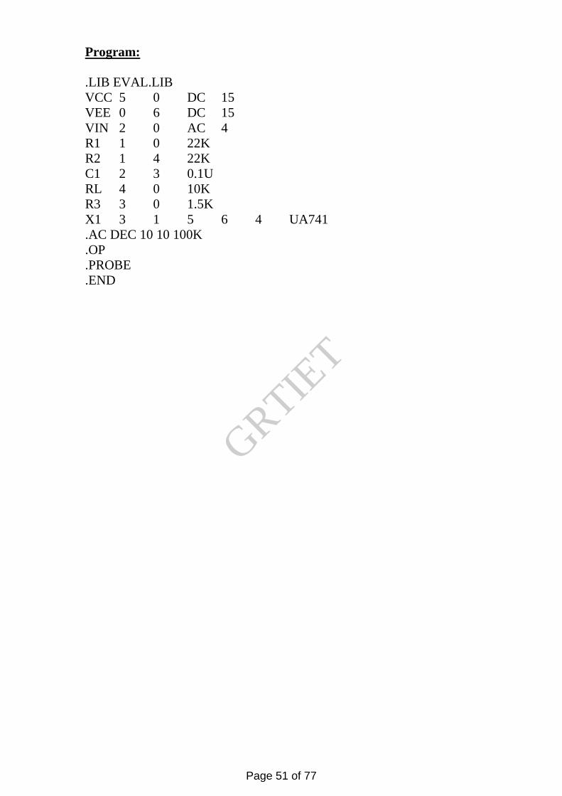
RC Phase shift Oscillator:
Page 60 of 77
GRTIET
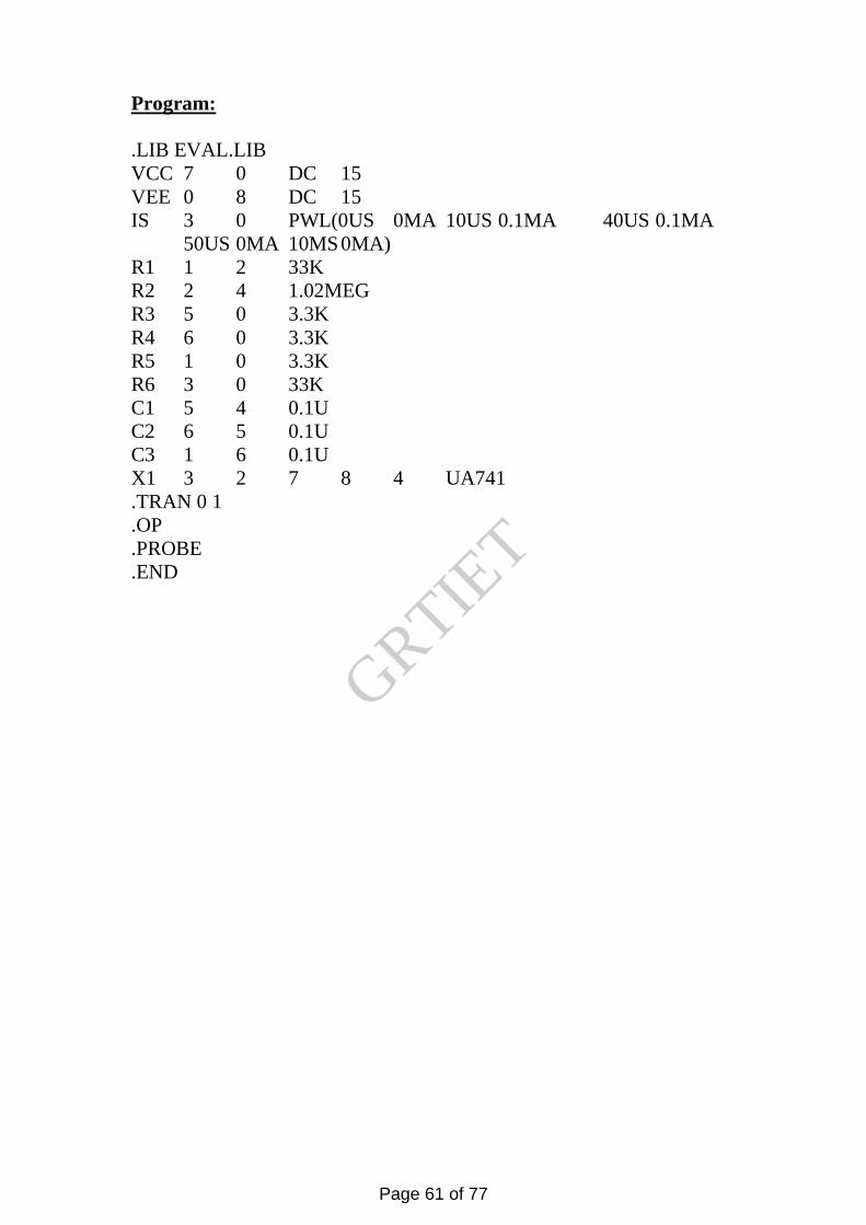
Program:
.LIB EVAL.LIB
VCC 7 0 DC 15
VEE 0 8 DC 15
IS 3 0 PWL(0US 0MA 10US 0.1MA 40US 0.1MA
50US 0MA 10MS 0MA)
R1 1 2 33K
R2 2 4 1.02MEG
R3 5 0 3.3K
R4 6 0 3.3K
R5 1 0 3.3K
R6 3 0 33K
C1 5 4 0.1U
C2 6 5 0.1U
C3 1 6 0.1U
X1 3 2 7 8 4 UA741
.TRAN 0 1
.OP
.PROBE
.END
Page 61 of 77
GRTIET

Wein Bridge Oscillator:
Page 62 of 77
GRTIET

Program:
.LIB EVAL.LIB
VCC 5 0 DC 15
VEE 0 6 DC 15
IS 2 0 PWL(0US 0MA 10US 0.1MA 40US 0.1MA
50US 0MA 10MS 0MA)
R1 1 0 15K
R2 1 4 30.2K
R3 2 3 1.5K
R4 2 0 1.5K
C1 3 4 0.1U
C2 2 0 0.1U
X1 2 1 5 6 4 UA741
.TRAN 0 1
.OP
.PROBE
.END
Page 63 of 77
GRTIET
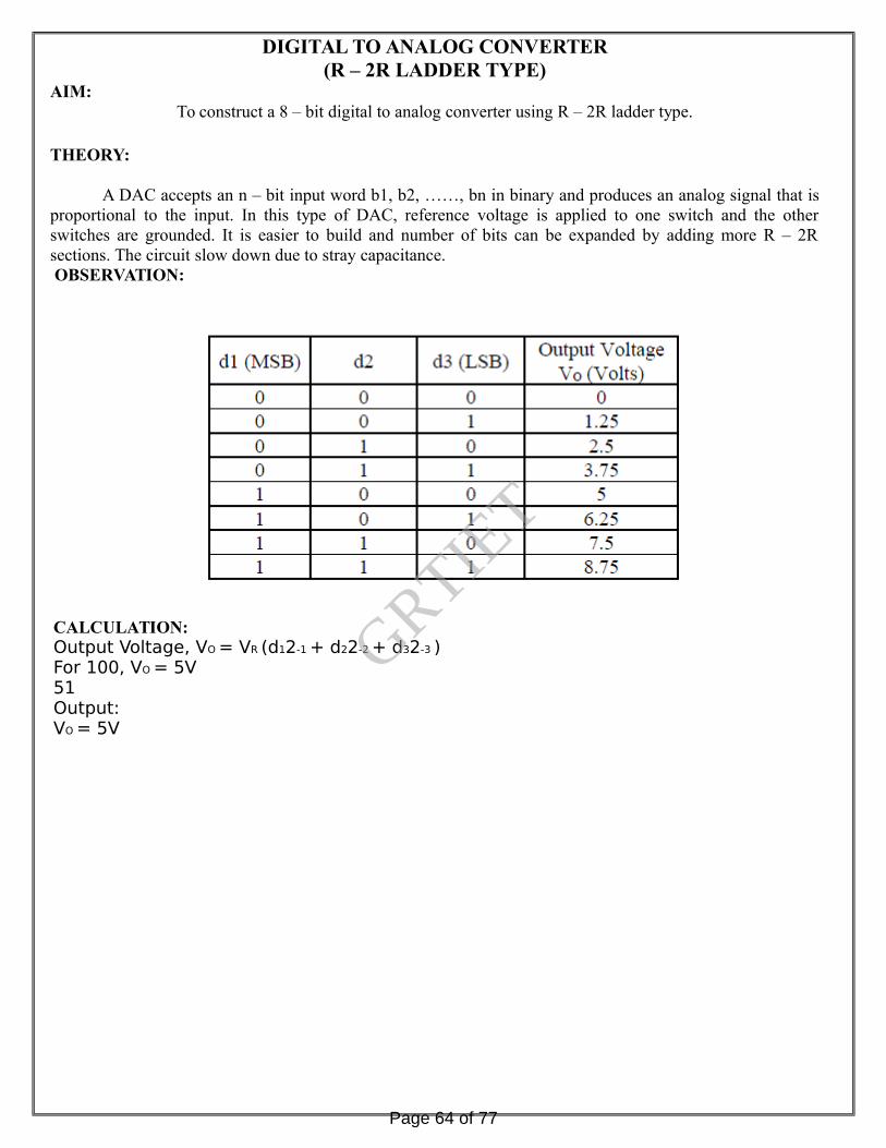
AIM:To construct a 8 – bit digital to analog converter using R – 2R ladder type.
THEORY:
A DAC accepts an n – bit input word b1, b2, ……, bn in binary and produces an analog signal that isproportional to the input. In this type of DAC, reference voltage is applied to one switch and the otherswitches are grounded. It is easier to build and number of bits can be expanded by adding more R – 2Rsections. The circuit slow down due to stray capacitance. OBSERVATION:
CALCULATION:Output Voltage, VO = VR (d12-1 + d22-2 + d32-3 )For 100, VO = 5V51Output:VO = 5V
DIGITAL TO ANALOG CONVERTER(R – 2R LADDER TYPE)
Page 64 of 77
GRTIET

CIRCUIT DIAGRAM
MODEL GRAPH:
RESULT:
Thus R – 2R ladder type digital to analog converter is implemented.
Page 65 of 77
GRTIET

ANALOG MULTIPLIER
AIM:
1. PC 2. PSPICE softwareTHEORY: Anolog multiplier is used to multiply two input singal. if a input is given to a log amplifier andthe output can be taken in the antilog amplifier.it is the simple way to test the multiplied signal.in this circuitit is designed using Ic.input is given to the terminals of two Ic’s and output is taken across . It is similar to logand antilog operation.
PROCEDURE:
1. Click on the start menu and select the p spice simulation software 2. Select the parts required for the circuit from the parts menu and place them in the work space 3. Connect the parts using wires 4. Save the file and select the appropriate analysis 5. Simulate the circuit and observe the corresponding output waveforms MODEL GRAPH
To simulate an Analog multiPLIER using PSPICE APPARATUS REQUIRED:
Page 66 of 77
GRTIET
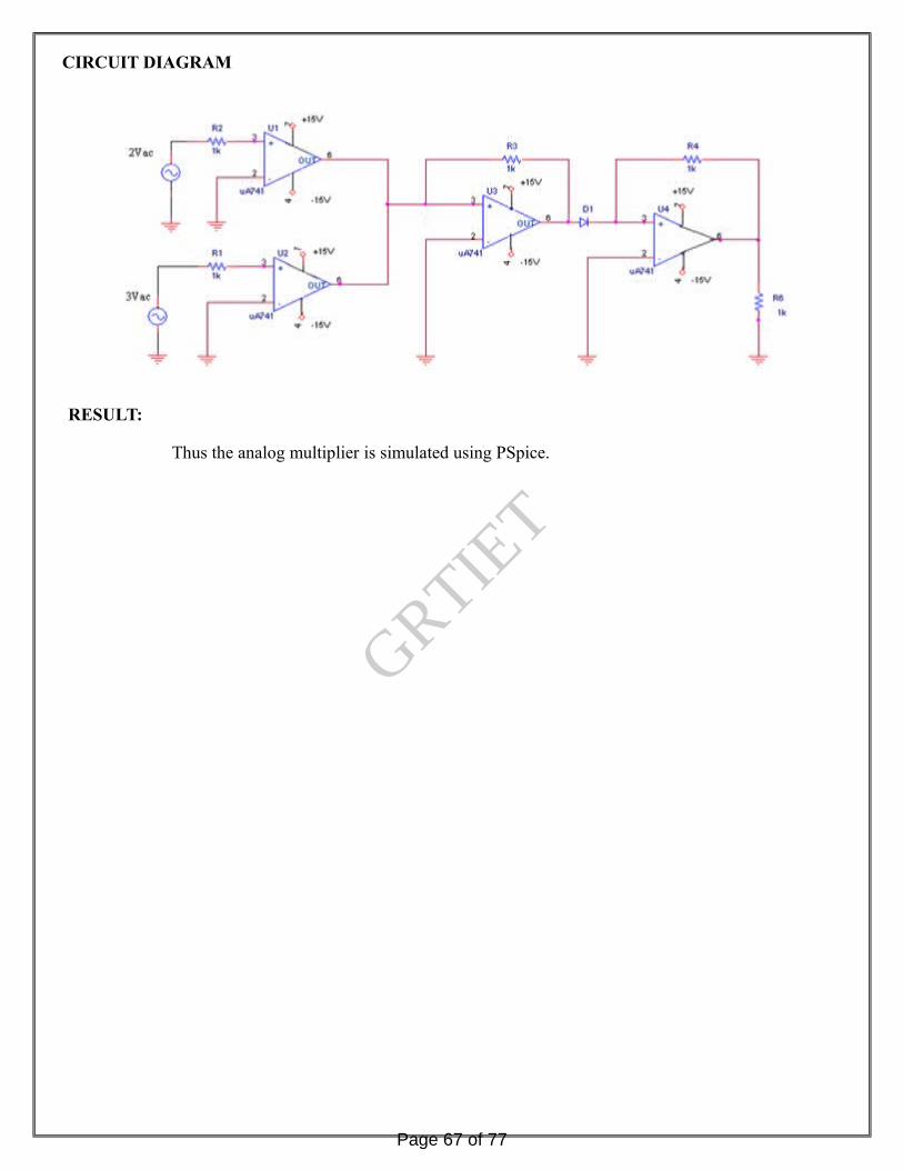
CIRCUIT DIAGRAM
Thus the analog multiplier is simulated using PSpice.
RESULT:
Page 67 of 77
GRTIET

CMOS Inverter, NAND and NOR using PSPICEAim:
To plot the transient characteristics of output voltage for the given CMOS inverter,NAND and NOR from 0 to 80m s in steps of 1m s. To calculate the voltage gain,input impedance and outputimpedance for the input voltage of 5V.
PARAMETER TABLE:
PARAMETRS PMOS NMOSL 1µ 1 µW 20 µ 5 µVTO -2 2KP 4.5e-4 2CBD 5p 5pCBS 2p 2pRD 5 5RB 0 0RS 2 2RG 0 0RDS 1Meg 1 MegCGSO 1p 1pCGDO 1p 1pCGBO 1p 1p
THEORY:
(i) InverterCMOS is widely used in digital IC’s because of their high speed, low power dissipation and it can be
operated at high voltages resulting in improved noise immunity. The inverter consists of two MOSFETs. Thesource of p-channel device is connected to +VDD and that of n-channel device is connected to ground. Thegates of two devices are connected as common input.(ii) NAND
It consists of two p-channel MOSFETs connected in parallel and two n-channel MOSFETs connectedin series. P-channel MOSFET is ON when gate is negative and N channel MOSFET is ON when gate ispositive. Thus when both input is low and when either of input is low, the output is high.(iii) NOR
It consists of two p-channel MOSFETs connected in series and two n-channel MOSFETs connected inparallel. P-channel MOSFET is ON when gate is negative and N-channel MOSFET is ON when gate ispositive. Thus when both inputs are high and when either of input is high, the output is low. When both theinputs are low, the output is high.R
Page 68 of 77
GRTIET

TRUTH TABLE INVERTER
NAND
NOR
CIRCUIT DIAGRAM
INVERTER
Page 69 of 77
GRTIET

NOR
NAND
Page 70 of 77
GRTIET

MODEL GRAPH
INVERTER
NAND
Page 71 of 77
GRTIET

Output:(i) InverterGain = V(2)/Vin =Input Resistance at Vin =Output Resistance at V(2) =(ii) NANDGain = V(4)/Vin1 = V(4)/Vin2 =Input Resistance at Vin1 =Input Resistance at Vin2 =Output Resistance at V(4) =(iii) NORGain = V(4)/Vin1 = V(4)/Vin2 =Input Resistance at Vin1 =Input Resistance at Vin2 =Output Resistance at V(4) =
InferrenceThus the transient characteristics of output voltage for the given CMOS inverter, NAND and
NOR is plotted and the voltage gain, input impedance and output impedance are calculated.
NOR
Page 72 of 77
GRTIET

AIM:
To design and test the operation of Summing amplifier.
EQUIPMENTS REQUIRED:
S.No Equipment andComponents
Range Quantity
1.2.3.4.5.6.7.
ResistorOp-ampDual RPSAFOCROBread boardConnecting wires
1,10,2kIC741(0-30)v
----
1,1,131111
few
THEORY:
The Summing Amplifier is a very flexible circuit based upon the standard Inverting operational amplifier configuration that can be used for combining multiple inputs. We saw previously in the inverting amplifier tutorial that the inverting amplifier has a single input voltage,Vin applied to the inverting input terminal. If we add more input resistors to the input, each equal in value to the original input resistor, Rin we end up with another operational amplifier circuit called a Summing Amplifier, “summing inverter" or even a "Voltage adder" circuit .The Summing Amplifier is a very flexible circuit indeed, enabling us to effectively "Add" or "Sum" together several individual input signals. If the inputs resistors, R1, R2, R3 etc, are all equal a unity gain inverting adder can be made. However, if the input resistors are of different values a "scaling summing amplifier" is produced which gives a weighted sum of the input signals. The
The gain of the circuit is
Gain(AV)=Vout/Vin=-Rf/Rin
A1=10k/1k=-10
A2=10k/2k=-5
Vout=(A1xV1)+(A2xV2)
we can now Vout=(-10(2mV))+(-5(5mV))=-45mv the values of the resistors in the circuit as follows,
DESIGN AND TESTING OF SUMMING AMPLIFIER
Page 73 of 77
GRTIET
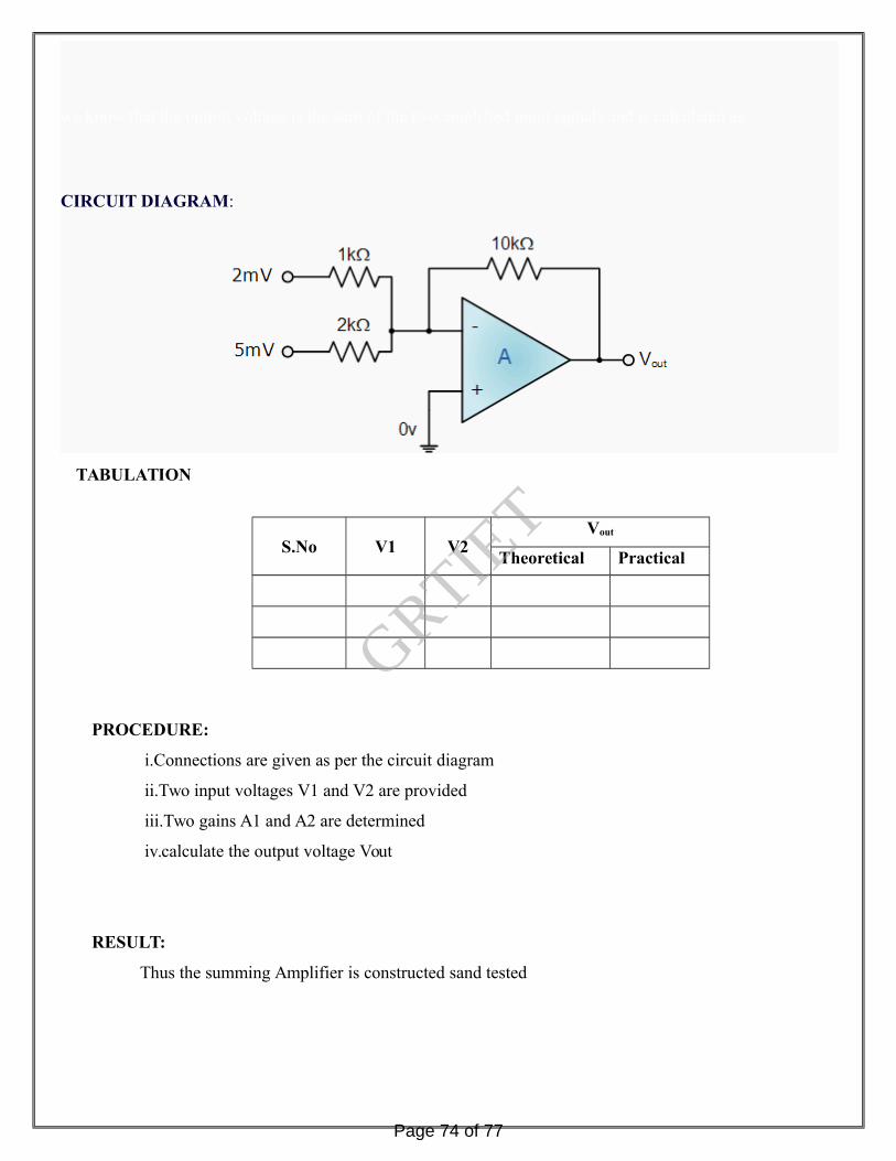
we know that the output voltage is the sum of the two amplified input signals and is calculated as:
CIRCUIT DIAGRAM:
TABULATION
PROCEDURE:
i.Connections are given as per the circuit diagram
ii.Two input voltages V1 and V2 are provided
iii.Two gains A1 and A2 are determined
iv.calculate the output voltage Vout
RESULT:
Thus the summing Amplifier is constructed sand tested
S.No V1 V2Vout
Theoretical Practical
Page 74 of 77
GRTIET
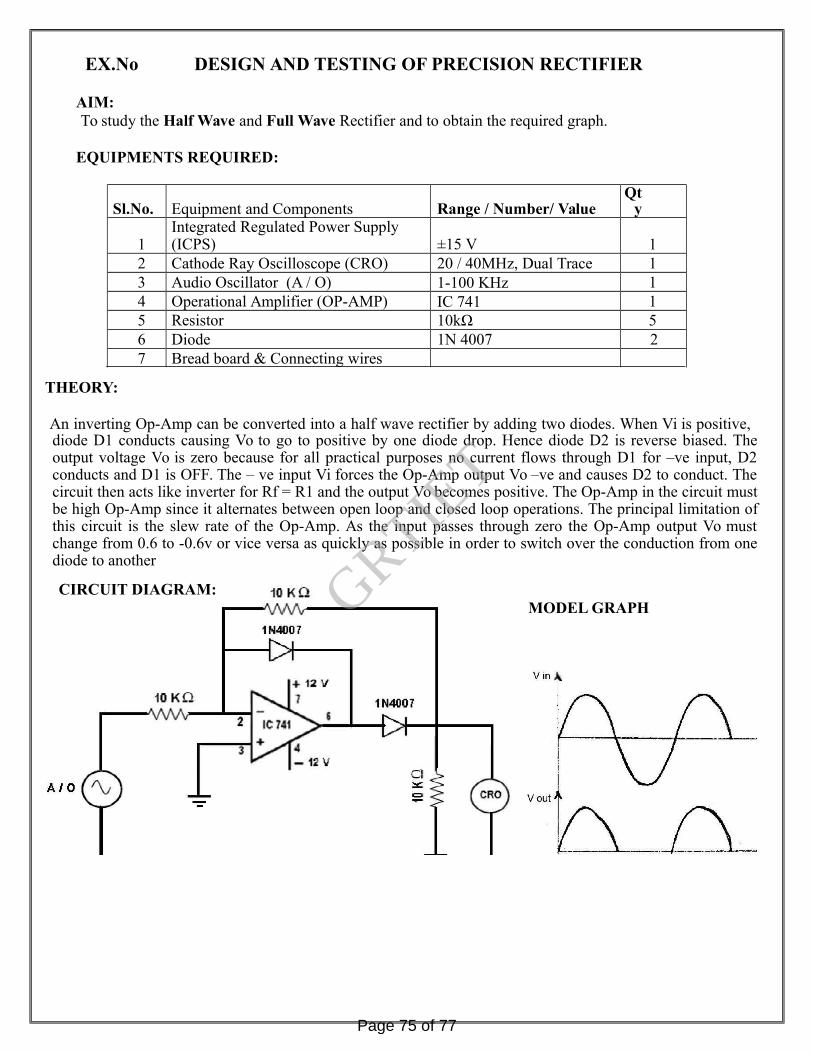
AIM:To study the Half Wave and Full Wave Rectifier and to obtain the required graph.
EQUIPMENTS REQUIRED:
Sl.No. Equipment and Components Range / Number/ ValueQt
y
1Integrated Regulated Power Supply (ICPS) ±15 V 1
2 Cathode Ray Oscilloscope (CRO) 20 / 40MHz, Dual Trace 13 Audio Oscillator (A / O) 1-100 KHz 14 Operational Amplifier (OP-AMP) IC 741 15 Resistor 10kΩ 56 Diode 1N 4007 27 Bread board & Connecting wires
THEORY:
An inverting Op-Amp can be converted into a half wave rectifier by adding two diodes. When Vi is positive,diode D1 conducts causing Vo to go to positive by one diode drop. Hence diode D2 is reverse biased. Theoutput voltage Vo is zero because for all practical purposes no current flows through D1 for –ve input, D2conducts and D1 is OFF. The – ve input Vi forces the Op-Amp output Vo –ve and causes D2 to conduct. Thecircuit then acts like inverter for Rf = R1 and the output Vo becomes positive. The Op-Amp in the circuit mustbe high Op-Amp since it alternates between open loop and closed loop operations. The principal limitation ofthis circuit is the slew rate of the Op-Amp. As the input passes through zero the Op-Amp output Vo mustchange from 0.6 to -0.6v or vice versa as quickly as possible in order to switch over the conduction from onediode to another
CIRCUIT DIAGRAM:MODEL GRAPH
EX.No DESIGN AND TESTING OF PRECISION RECTIFIER
Page 75 of 77
GRTIET

MODEL GRAPH :
FULL WAVE PRECISION RECTIFIER
TABULATION:
Sl.No.Input Output
Description Amplitude Time Amplitude Time
1Half Wave
2Full Wave
Page 76 of 77
GRTIET

PROCEDURE:1.Connections are made as per the circuit diagram2.A sinusoidal signal from audio oscillator is applied to the inverting terminal of op-*amp3.The rectified output is then obtained on the CRO.
RESULT:The Half Wave and Full Wave Precision rectifier is constructed and output is obtained.
Page 77 of 77
GRTIET