Growth and Structural Characterizations of Nanostructured Chromium
5
Growth and Structural Characterizations of Nanostructured Chromium-Zirconium-Nitride Thin Films for Tribological Applications Pattira Homhuan 1; * 1 , Surasing Chaiyakun 2 , Rattaporn Thonggoom 3;4 , Nurot Panich 5 and Sukkaneste Tungasmita 5;6; * 2 1 Nanoscience and Technology, Graduate School, Chulalongkorn University, Bangkok, 10330, Thailand 2 Department of Physics, Faculty of Science, Burapa University, Chonburi, 20131, Thailand 3 Department of Chemistry, Faculty of Science, Mahidol University, Bangkok, 10400, Thailand 4 Center for Surface Science and Engineering, Faculty of Science, Mahidol University, Bangkok, 10400, Thailand 5 Center of Innovative Nanotechnology, Chulalongkorn University, Bangkok, 10330, Thailand 6 Department of Physics, Faculty of Science, Chulalongkorn University, Bangkok, 10330, Thailand Nanostructured Cr-Zr-N thin films were grown on Si(100) substrates in a mixture of Ar and N 2 plasma. The nitrogen partial pressure was varied to produce and control the stoichiometric forms obtained. All the Cr-Zr-N films exhibited a nanostructure with an average grain size of less than 10 nm, as determined by X-ray diffractogram analysis, and were formed in the solid-solution. As the contents of nitrogen in the film increased, it lead to changes in the crystal texture and competitive growth. The maximum root mean square roughness was 7.87 nm at a 20% nitrogen partial pressure and the roughness tended to decrease as the grain size decreased. The nano-indentation showed that the films grown at a 20% nitrogen partial pressure and annealed at 700 C had the highest reduced modulus and hardness at 349.2 and 35.1 GPa, respectively. The mechanical properties of films can be improved by a post-annealing heat treatment. With respect to the electrical properties of these films, the sheet resistance, which is related to the defect level, tended to increase as the nitrogen partial pressure increased. [doi:10.2320/matertrans.M2010140] (Received April 20, 2010; Accepted June 10, 2010; Published July 28, 2010) Keywords: magnetron sputtering, nanostructure, hard coating, protective thin films 1. Introduction Transition-metal-nitride thin films deposited by physical vapor deposition (PVD) have been developed and used as mechanically and chemically protective layers for industrial applications for many years. The cubic-base structural chromium nitride (CrN) is a more recent and interesting choice of such layers due to its well-matched properties to some industrial requirements, especially those that require a hard coating and for tribological applications. This is largely due to the fact that CrN films have a high hardness, high wear- and corrosion-resistance, and also have a low friction- coefficient. 1,2) Adding one more metal element to form Cr-based ternary nitride films has been reported to show improved properties compared to the binary CrN com- pound. 3–5) However, in the case of Zn, as an example added tertiary metal element, there is an apparent lack of important information about the properties of the ternary Cr-Zr-N films derived from various growth parameters, despite the fact that these are the key variables for engineering the desired properties of the material. In this work, we explored the role of the nitrogen partial pressure during film formation, and that of the post-process annealing temperature, on the structural, mechanical and electrical properties of the re- sultant Cr-Zr-N film. 2. Experimental Procedures Ternary Cr-Zr-N films were grown by dual unbalanced D.C. magnetron sputtering with horizontal magnetron sources on Si(100) substrates. All films were produced from pure Cr and Zr targets in a defined mixture of Ar and N 2 plasma. The base pressure in this reactive sputtering system was pumped down to 5 10 5 mbar. The partial pressure of nitrogen (N 2 =Ar þ N 2 ) during the process was varied to produce various compositions of films. During the formation of films, the discharge current of each target was controlled at a constant 0.5 A. All films were grown without an extra heat source, except the transferred energy at the substrate surface from the collision of adatoms and plasma species. In this work, the substrate was at a floating potential. The thickness of all the films obtained was in the range of 0.9–2.0 mm, depending on the nitrogen partial pressure used during their growth. The elemental composition of each film was measured by energy dispersive spectroscopy (EDS) (Oxford INCA), coupled to a scanning electron microscope (JEOL JSM- 6480LV), that was also used for scanning electron microcopy (SEM). For the structural characterization of films, the specimens were characterized by X-ray diffraction (XRD) (Brukers D8 Discover) with Cu K (! ¼ 0:15406 nm) as the X-ray source. The cross-sectional microstructure was investigated by transmission electron microscopy (TEM) (JEOL JEM-2010 200 kV transmission electron microscope). The surface topography was investigated by atomic force microscopy (AFM) (Veeco Nanoscope-IV). The hardness and reduced modulus were both measured using a Micro Material Nano Test in the constant depth mode with a Berkovich pyramidal indenter tip. To avoid the effect of substrate, the depth of indentation was limited to less than 1/10 that of the film thickness, which in this case meant the depth was taken at about 100 nm. The sheet-resistance of the film material was evaluated by the van der Pauw method. The * 1 Graduate Student, Chulalongkorn University * 2 Corresponding author, E-mail: [email protected] Materials Transactions, Vol. 51, No. 9 (2010) pp. 1651 to 1655 #2010 The Japan Institute of Metals
Transcript of Growth and Structural Characterizations of Nanostructured Chromium

Growth and Structural Characterizations of Nanostructured
Chromium-Zirconium-Nitride Thin Films for Tribological Applications
Pattira Homhuan1;*1, Surasing Chaiyakun2, Rattaporn Thonggoom3;4,Nurot Panich5 and Sukkaneste Tungasmita5;6;*2
1Nanoscience and Technology, Graduate School, Chulalongkorn University, Bangkok, 10330, Thailand2Department of Physics, Faculty of Science, Burapa University, Chonburi, 20131, Thailand3Department of Chemistry, Faculty of Science, Mahidol University, Bangkok, 10400, Thailand4Center for Surface Science and Engineering, Faculty of Science, Mahidol University, Bangkok, 10400, Thailand5Center of Innovative Nanotechnology, Chulalongkorn University, Bangkok, 10330, Thailand6Department of Physics, Faculty of Science, Chulalongkorn University, Bangkok, 10330, Thailand
Nanostructured Cr-Zr-N thin films were grown on Si(100) substrates in a mixture of Ar and N2 plasma. The nitrogen partial pressure wasvaried to produce and control the stoichiometric forms obtained. All the Cr-Zr-N films exhibited a nanostructure with an average grain size ofless than 10 nm, as determined by X-ray diffractogram analysis, and were formed in the solid-solution. As the contents of nitrogen in the filmincreased, it lead to changes in the crystal texture and competitive growth. The maximum root mean square roughness was 7.87 nm at a 20%nitrogen partial pressure and the roughness tended to decrease as the grain size decreased. The nano-indentation showed that the films grown at a20% nitrogen partial pressure and annealed at 700�C had the highest reduced modulus and hardness at 349.2 and 35.1GPa, respectively. Themechanical properties of films can be improved by a post-annealing heat treatment. With respect to the electrical properties of these films, thesheet resistance, which is related to the defect level, tended to increase as the nitrogen partial pressure increased.[doi:10.2320/matertrans.M2010140]
(Received April 20, 2010; Accepted June 10, 2010; Published July 28, 2010)
Keywords: magnetron sputtering, nanostructure, hard coating, protective thin films
1. Introduction
Transition-metal-nitride thin films deposited by physicalvapor deposition (PVD) have been developed and used asmechanically and chemically protective layers for industrialapplications for many years. The cubic-base structuralchromium nitride (CrN) is a more recent and interestingchoice of such layers due to its well-matched properties tosome industrial requirements, especially those that require ahard coating and for tribological applications. This is largelydue to the fact that CrN films have a high hardness, highwear- and corrosion-resistance, and also have a low friction-coefficient.1,2) Adding one more metal element to formCr-based ternary nitride films has been reported to showimproved properties compared to the binary CrN com-pound.3–5) However, in the case of Zn, as an example addedtertiary metal element, there is an apparent lack of importantinformation about the properties of the ternary Cr-Zr-N filmsderived from various growth parameters, despite the factthat these are the key variables for engineering the desiredproperties of the material. In this work, we explored therole of the nitrogen partial pressure during film formation,and that of the post-process annealing temperature, on thestructural, mechanical and electrical properties of the re-sultant Cr-Zr-N film.
2. Experimental Procedures
Ternary Cr-Zr-N films were grown by dual unbalancedD.C. magnetron sputtering with horizontal magnetron
sources on Si(100) substrates. All films were produced frompure Cr and Zr targets in a defined mixture of Ar and N2
plasma. The base pressure in this reactive sputtering systemwas pumped down to 5� 10�5 mbar. The partial pressureof nitrogen (N2=Arþ N2) during the process was varied toproduce various compositions of films. During the formationof films, the discharge current of each target was controlled ata constant 0.5A. All films were grown without an extra heatsource, except the transferred energy at the substrate surfacefrom the collision of adatoms and plasma species. In thiswork, the substrate was at a floating potential. The thicknessof all the films obtained was in the range of 0.9–2.0 mm,depending on the nitrogen partial pressure used during theirgrowth.
The elemental composition of each film was measuredby energy dispersive spectroscopy (EDS) (Oxford INCA),coupled to a scanning electron microscope (JEOL JSM-6480LV), that was also used for scanning electron microcopy(SEM). For the structural characterization of films, thespecimens were characterized by X-ray diffraction (XRD)(Brukers D8 Discover) with Cu K� (� ¼ 0:15406 nm) asthe X-ray source. The cross-sectional microstructure wasinvestigated by transmission electron microscopy (TEM)(JEOL JEM-2010 200 kV transmission electron microscope).The surface topography was investigated by atomic forcemicroscopy (AFM) (Veeco Nanoscope-IV).
The hardness and reduced modulus were both measuredusing a Micro Material Nano Test in the constant depth modewith a Berkovich pyramidal indenter tip. To avoid the effectof substrate, the depth of indentation was limited to less than1/10 that of the film thickness, which in this case meant thedepth was taken at about 100 nm. The sheet-resistance of thefilm material was evaluated by the van der Pauw method. The
*1Graduate Student, Chulalongkorn University*2Corresponding author, E-mail: [email protected]
Materials Transactions, Vol. 51, No. 9 (2010) pp. 1651 to 1655#2010 The Japan Institute of Metals

stoichiometric Cr-Zr-N films grown at a 20% nitrogen partialpressure were used for the study of the effect of the post-growth annealing temperature under an Ar flow at vacuumpressure for 1 h, and then cooled down. The ramping rate ofthe annealing reaction was 5�C/min.
3. Results and Discussion
3.1 Effect of nitrogen partial pressure3.1.1 Chemical composition
The elemental concentrations of Cr, Zr and N in the as-deposited films on silicon (100) substrates derived underdifferent nitrogen partial pressures are shown in Fig. 1.The nitrogen composition in the films increased essentiallylinearly with increasing nitrogen partial pressure up to anitrogen partial pressure of 20%, and thereafter remainedalmost constant and largely numerically and statisticallyindependent of the nitrogen partial pressure. This representsthe saturated condition for nitrogen atoms incorporation intothe film material. Moreover, at all nitrogen partial pressures,there was a higher concentration of Cr than Zr, because Crhas a higher sputtering yield compared to that for Zr.6) Byincreasing the nitrogen partial pressure, the reaction ratebetween nitrogen and metal at the target surface increases,which causes the sputtered nitrogen atoms and some of themetal-nitrogen cluster particles from the surface target to alsoincrease.7) In contrast, the relative proportion of sputteredZr and Cr atoms from the surface target that form filmsdecreases due to the increased coverage of nitrogen on thesurface, resulting in the formation of metal nitride on thesurface of the metallic target. The sputter yield for the nitridematerial at the target surface is much lower than that for themetal, which causes the deposition rate of films to decreaseas the percentage of nitrogen partial pressure increases (seeFig. 2).3.1.2 Structural properties
Figure 3 shows representative X-ray diffraction (XRD)spectra of the Cr-Zr-N films grown under the differentnitrogen partial pressures, plotted on a semi-log scale. Sincethe Cr-Zr-N ternary compound came from the combination ofCrN and ZrN materials, which alone both have a rock-salt
NaCl type crystal structure, then the Cr-Zr-N also seems toretain a NaCl-like crystal structure. The peak positions forsome major orientations of the Cr-Zr-N materials as afunction of the Zr/Cr ratio have been calculated andpresented elsewhere.4) Here, according to EDS results, thecomposition of the material becomes stable after a 20%nitrogen partial pressure was applied and exhibits a patternsimilar to the Cr0:7Zr0:3N form in the ICDD 03-065-9004database, with a NaCl-like structure. The Cr0:7Zr0:3N(200)form starts to develop from a nitrogen partial pressure of15%, whilst the (200) plane is the preferable orientationwhen formed over and above a 15% nitrogen partialpressure because of the dominant surface energy. TheCr0:7Zr0:3N(200) is more stable and has the lowest surfaceenergy.8) However, the lowest strain energy is found withCr0:7Zr0:3N(111) and is the preferred orientation for CrN atlow temperature growth.9) Accordingly, the developmentof texture in the Cr-Zr-N films can be changed from thatof CrN alone by control of the ternary metal and nitrogenpartial pressure. This can be explained by re-nucleation,due to the addition of zirconium in the films.10) Whilst theformation (detection) of both the Cr0:7Zr0:3N(111) and theCr0:7Zr0:3N(220) forms started to appear at a 20% nitrogenpartial pressure, as the nitrogen partial pressure increases
Fig. 1 Elemental concentrations of Cr-Zr-N films formed with different
nitrogen partial pressures. Elemental concentrations are shown for N
(triangles), Cr (squares) and Zr (circles).
Fig. 2 Deposition rate of Cr-Zr-N films as a function of the nitrogen partial
pressure.
Fig. 3 Representative XRD spectra of Cr-Zr-N films grown at the indicated
different nitrogen partial pressures.
1652 P. Homhuan, S. Chaiyakun, R. Thonggoom, N. Panich and S. Tungasmita

further above 20% the position of these peaks shifts slightlytowards the lower diffraction angles. This may be related toan increase in the compressive stress in the film due to theformation of a solid solution.10) In addition, changes in theatomic density of the crystalline films can be considered. Thedensity values of (200), (220) and (111) represent 4, 2.83 and2.31 at/a2, respectively. As the nitrogen partial pressureincreases, so the adatoms are arranged to form films in lowerdensity planes because the mobility of the adatoms is limited,and the energy of sputtered atoms decreases with increasingin the nitrogen partial pressures.11)
The size of the formed grains was evaluated from the XRDpeaks using the Scherer formula. All films have a grain sizeof less than 10 nm, but are perhaps even smaller since thisvalue ignores the fact that the peak can be broad from theresidual stress.12) Therefore, the result indicates that all thefilms were conform to a Zone 1 model in the Thornton’sstructure zone model, with a low substrate temperature.In this zone, adatoms have a low surface diffusion becauseof a low substrate temperature and, since the adatoms areinsufficient to overcome the shadowing effect, the films havea typical small-width columnar structure with voids with arough surface.13,14)
3.1.3 Cross-sectional and surface morphologyThe surface morphology of the Cr-Zr-N films, as evaluated
by AFM, as a function of the nitrogen partial pressure isshown in Fig. 4. The maximum root mean square roughnesswas 7.87 nm at a 20% nitrogen partial pressure, because ofthe competition among the Cr-Zr-N(111), (200) and (220),whilst the roughness tended to decrease as the grain sizedecreased.15) A typical TEM micrograph of a Cr-Zr-N filmgrown at a 20% nitrogen partial pressure is shown in Fig. 5,along with an electron diffraction pattern. The microstructureof the film has a clear dense columnar structure, with somevoids visible in the film material, whilst the average domainsize is about or less than 10 nm. This particle domain sizeconforms well to that calculated from the XRD data.3.1.4 Mechanical properties
With respect to the mechanical properties of hard coatings,the hardness and reduced modulus are the two most importantproperties of films and so were evaluated. Both the hardnessand the reduced modulus of the Cr-Zr-N films, plotted as afunction of the nitrogen partial pressure, were maximal whenformed under a 20% nitrogen partial pressure (Fig. 6). Attheir maximum hardness and reduced modulus (30.0 and324.1GPa, respectively), they were nearly stoichiometric
with a Zr0:3Cr0:7N form that was in good agreement with thatfor ICDD 03-065-9004 in the database. From these results theroughness and grain diameter appear to be related to thehardness, as there is competition among (111), (200) and(220) planes. Moreover, the hardness strongly depends on thenitrogen contents in the films, as shown by the dose-dependence to the nitrogen partial pressure over from 0 to20% range. This maximum hardness of the Cr-Zr-N film,when grown at a 20% nitrogen partial pressure, consists of
Fig. 4 Representative AFM images of Cr-Zr-N films formed under different nitrogen partial pressures of (a) 6%, (b) 20%, (c) 50% and
(d) 100%.
Fig. 5 Representative cross-sectional micrograph of a Cr-Zr-N film formed
at a 20% nitrogen partial pressure, with an electron diffraction pattern
shown in the insert.
Fig. 6 Hardness and reduced modulus of Cr-Zr-N films as a function of the
nitrogen partial pressure.
Growth and Structural Characterizations of Nanostructured Chromium-Zirconium-Nitride Thin Films for Tribological Applications 1653
the maximum amount of nitrogen completely bonded withmetallic atoms.16) However, that it then declines with furtherincreases in nitrogen partial pressures, rather than remains atsame saturation level, is due to the fact that higher partialpressures of nitrogen lead to a larger excess of nitrogen in thefilms located in the interstitial sites. This form of solidsolution has a high hardness because the Zr atoms, whichsubstitute for the Cr atoms in the face-center-cubic-structure,are limited to the mobility of dislocation.
The strength of adhesion between each of the different Cr-Zr-N films and the silicon (100) substrate was tested by nano-scratch, where the critical load is determined by a suddenchange in the penetration depth in scratch tests. By thismethod, a maximum critical load (LC) of 2.1 N was obtainedwith films produced at a 15% nitrogen partial pressure, anddecreased thereafter at higher nitrogen partial pressures (datanot shown). Thus, Cr-Zr-N films grown at a 15% nitrogenpartial pressure had the best adhesion to the silicon (100)substrate. That the adhesion of films tended to decrease as thenitrogen partial pressure was increased is because theadatoms under these conditions have less energy to formfilms.3.1.5 The electrical properties
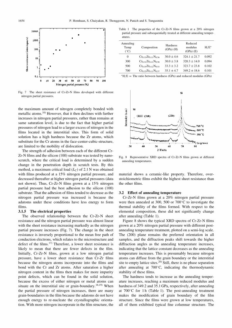
The observed relationship between the Cr-Zr-N sheetresistance and the nitrogen partial pressure was almost linearwith the sheet resistance increasing markedly as the nitrogenpartial pressure increases (Fig. 7). The change in the sheetresistance is inversely proportional to the mean free path ofconduction electrons, which relates to the microstructure anddefect of the films.17) Therefore, a lower sheet resistance islikely to mean that there are fewer defects in the film.Initially, Cr-Zr-N films, grown at a low nitrogen partialpressure, have a lower sheet resistance than Cr-Zr filmsbecause the nitrogen atoms incorporate into the films andbond with the Cr and Zr atoms. After saturation a highernitrogen content in the films then makes for more impuritypoint defects, which can be found in the solid solution,because the excess of either nitrogen or metal atoms cansituate on the interstitial site or grain-boundary.18,19) Whenthe partial pressure of nitrogen increases, there are manygrain-boundaries in the film because the adatoms do not haveenough energy to re-nucleate the crystallographic orienta-tion. With more nitrogen incorporate in the film structure, the
material shows a ceramic-like property. Therefore, over-stoichiometric films exhibit the highest sheet resistance thanthe other films.
3.2 Effect of annealing temperatureCr-Zr-N films grown at a 20% nitrogen partial pressure
were then annealed at 300, 500 or 700�C to investigate thethermal stability of the films formed. With respect to theelemental composition, these did not significantly changeafter annealing (Table 1).
Figure 8 shows the typical XRD spectra of Cr-Zr-N filmsgrown at a 20% nitrogen partial pressure with different post-annealing temperature treatment, plotted on a semi-log scale.The (200) plane remains the preferred orientation in allsamples, and the diffraction peaks shift towards the higherdiffraction angles as the annealing temperature increases,indicating that the lattice constant decreases as the annealingtemperature increases. This is presumably because nitrogenatoms can diffuse from the grain boundary or the interstitialsite to empty lattice sites.20) Still, there is no phase separationafter annealing at 700�C, indicating the thermodynamicstability of these films.
The hardness tends to increase as the annealing temper-ature increases, reaching a maximum reduced modulus andhardness of 349.2 and 35.1 GPa, respectively, after annealingat 700�C for 1 h (Table 1). The post-annealing treatmentmakes the modification of grain boundary of the filmstructure. Since the films were grown at low temperatures,all of them exhibited typical fine columnar structure. The
Fig. 7 The sheet resistance of Cr-Zr-N films developed with different
nitrogen partial pressures.
Table 1 The properties of the Cr-Zr-N films grown at a 20% nitrogen
partial pressure and subsequentially treated at different annealing temper-
atures.
Annealing
Temp
(�C)
CompositionHardness
(GPa) (H)
Reduced
modulus
(GPa) (E)
H/E�
0 Cr0:33Zr0:11N0:56 30:0� 4:6 324:1� 21:7 0.092
300 Cr0:31Zr0:11N0:58 30:0� 3:8 320:3� 14:0 0.094
500 Cr0:35Zr0:12N0:53 33:3� 3:2 323:7� 23:8 0.102
700 Cr0:32Zr0:11N0:57 35:1� 4:7 349:2� 18:6 0.101
�H/E = The ratio between hardness (GPa) and reduced modulus (GPa)
Fig. 8 Representative XRD spectra of Cr-Zr-N films grown at different
annealing temperatures.
1654 P. Homhuan, S. Chaiyakun, R. Thonggoom, N. Panich and S. Tungasmita

post-annealing process can cause lattice vibration andintroduces grain boundary annihilation mechanism. Thisresults in an increasing of domain width and the changing incrystal structure.
The wear resistance of the films can be found from theratio between the hardness and modulus,21) and revealed thatCr-Zr-N films grown at a 20% nitrogen partial pressure andannealed at 500�C had the maximum value (highest wearresistance). After annealing, the RMS roughness was notchanged (Fig. 9).
4. Conclusions
Chromium zirconium nitride films were grown at differentnitrogen partial pressures (0–100%) on silicon (100) sub-strates. The nitrogen partial pressure was observed to play animportant role in the stoichiometry, microstructure, deposi-tion rate, surface morphology, sheet-resistance and hardnessof the obtained Cr-Zr-N films due to the incorporation ofnitrogen into the films. This phenomenon leads to thecreation, and competitive growth, of the texture and surfaceroughness of the films. The films developed from a randomoriented crystalline structure to a texture-crystalline structureat nitrogen partial pressures of 15%. The solid solutionmaterial was formed without any evidence of phase separa-tion between the CrN and the ZrN. The hardness of the filmdid not seem to significantly depend on the content ofnitrogen, but rather was related to the equilibrium site. TheCr0:32Zr0:11N0:57 film, grown at a 20% nitrogen partialpressure and annealed at 700�C, had the highest hardnessand reduced modulus. The sheet resistance of Cr-Zr-N filmstended to increase with increasing nitrogen partial pressure.The films had thermal stability up to 700�C.
Acknowledgements
The authors would like to thank Mr. NuttapongParncharoenthaworn for helping measure the nanoindenta-tion and The Commission on Higher Education and Graduate
Thesis Grant for financial support that enabled this researchwork to be performed.
REFERENCES
1) J. Lin, Z. L. Wu, X. H. Zhang, B. Mishra, J. J. Moore andW. D. Sproul:
Thin Solid Films 517 (2009) 1887–1894.
2) S. H. Shin, M. W. Kim, M. C. Kang, K. H. Kim, D. H. Kwon and J. S.
Kim: Surf. Coat. Technol. 202 (2008) 5613–5616.
3) S. M. Aouadi, T. Maeruf, R. D. Twesten, D. M. Mihut and S. L. Rohde:
Surf. Coat. Technol. 200 (2006) 3411–3417.
4) G. S. Kim, B. S. Kim, S. Y. Lee and J. H. Hahns: Surf. Coat. Technol.
200 (2005) 1669–1675.
5) R. Lamni, R. Sanjines, M. Parlinska-Wojtan, A. Karimi and F. Levy:
J. Vac. Sci. Technol. A 23 (2005) 593–598.
6) G. E. McGuire (Ed): Semiconductor Materials and Process Technology
Handbook for Very Large Scale Integration (VLSI) and Ultra Large
Scale Integration (ULSI), (Noyes Publications, New Jersey, 1988)
p. 373.
7) S. Hofmann: Thin Solid Films 191 (1990) 335–348.
8) J. L. Ruan, J. L. Huang, J. S. Chen and D. F. Lii: Surf. Coat. Technol.
200 (2005) 652–1658.
9) P. Homhoul, C. Thavornthira, S. Chaiyakun and S. Tungasmita: J. Sci.
Res. Chula Uni. 33 (2008) 43–49.
10) G. Ababias: Surf. Coat. Technol. 202 (2008) 2223–2235.
11) L. Combadiere and J. Machet: Surf. Coat. Technol. 88 (1996) 17–27.
12) S. Ulrich, H. Holleck, J. Ye, H. Leiste, R. Loos, M. Stuber, P. Pesch and
S. Sattel: Thin Solid Films 437 (2003) 164–169.
13) S. PalDey and S. C. Deevi: Mater. Sci. Eng. A 342 (2003) 58–79.
14) G. E. McGuire (Ed): Semiconductor Materials and Process Technology
Handbook for Very Large Scale Integration (VLSI) and Ultra Large
Scale Integration (ULSI), (Noyes Publications, New Jersey, 1988)
p. 415.
15) Z. X. Song, Y. Wang, C. J. F. Wang, C. L. Liu and K. W. Xu: Surf.
Coat. Technol. 202 (2007) 5412–5415.
16) R. D. Arnell, J. S. Colligon, K. F. Minnebaev and V. E. Yurasova:
Vacuum 47 (1996) 425–431.
17) Y. K. Lee, J. Y. Kim, Y. K. Lee, M. S. Lee, D. K. Kim, D. Y. Jin, T. H.
Nam, H. J. Ahn and D. K. Park: J. Crystal Growth 234 (2002) 498–504.
18) L. Hulman, U. Helmersson, S. A. Barnett, J.-E. Sundgren and J. E.
Greene: J. Appl. Phys. 61 (1987) 552–555.
19) D. William and Jr. Callister: Material Science and Engineering an
Introduction 6 ed., (John Wiley&Sons, 2003) p. 77.
20) L. Hultman: Vacuum 57 (2000) 1–30.
21) P. K. Huang and J. W. Yeh: Surf. Coat. Technol. 203 (2009) 1891–
1896.
Fig. 9 Representative AFM images of Cr-Zr-N films; (a) as-deposited specimen, and specimens annealed at (b) 300�C, (c) 500�C and
(d) 700�C.
Growth and Structural Characterizations of Nanostructured Chromium-Zirconium-Nitride Thin Films for Tribological Applications 1655