Group IV Nano Optoelectronics: Si Nano Optoelectronics€¦ · Lorenzo Pavesi and David J....
18
US-Korea Nano-Forum 2009 POSTECH, Nano Device Materials and Physics Lab The 6 th US-Korea Forums on Nanotechnology: Nanoelectronics and its Integration with Applications April 29. 2009 Moon-Ho Jo Dept. of Materials Science and Engineering Pohang University of Science and Technology (POSTECH) Group IV Nano Optoelectronics: Recent Developments based on Bottom-Up Approaches
Transcript of Group IV Nano Optoelectronics: Si Nano Optoelectronics€¦ · Lorenzo Pavesi and David J....

US-Korea Nano-Forum 2009 POSTECH, Nano Device Materials and Physics Lab
Si Nano Optoelectronics: Recent Developments based on Bottom-Up Approaches
The 6th US-Korea Forums on Nanotechnology:Nanoelectronics and its Integration with Applications
April 29. 2009
Moon-Ho Jo
Dept. of Materials Science and EngineeringPohang University of Science and Technology (POSTECH)
Group IV Nano Optoelectronics: Recent Developments based on Bottom-Up Approaches
US-Korea Nano-Forum 2009 POSTECH, Nano Device Materials and Physics Lab
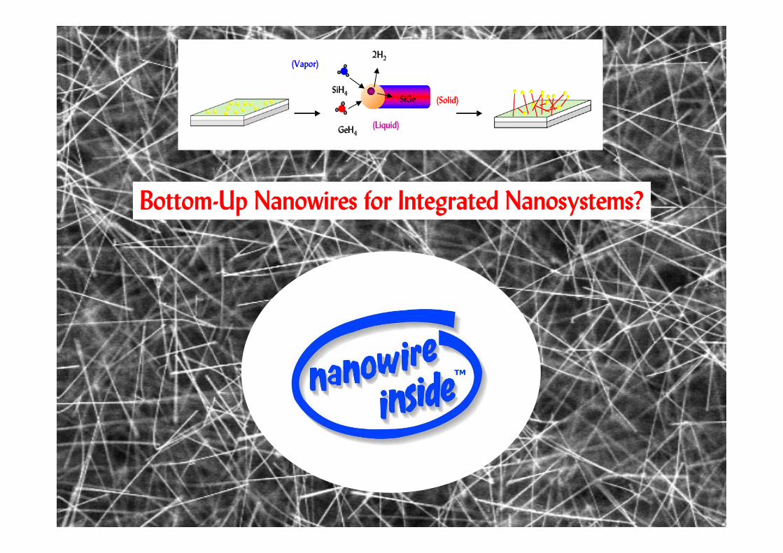
Bottom-Up Nanowires for Integrated Nanosystems?
(Liquid)
(Solid)SiH4
2H2
SiGe
GeH4
(Vapor)

US-Korea Nano-Forum 2009 POSTECH, Nano Device Materials and Physics Lab
1. Unique size effects at the individual NW level
Nanowire Photonics/Optoelectronics/Photovoltaics
2. Large-area integrated NW arrays

US-Korea Nano-Forum 2009 POSTECH, Nano Device Materials and Physics Lab
20 nm
0.209nm
2 nm20 nm20 nm
0.209nm
2 nm
0.209nm
2 nm2 nm
SiO2/Si
[Visible] [Near Infrared]1.55μm 1.35μm [Ultraviolet]
Nature Phys., Accepted (2009) Nano Lett., Accepted (2009)Appl. Phys. Lett., In Press (2009) Appl. Phys. Lett., 92 263111 (2008)Nano Lett. 6 2679 (2006)
Nanowire Electronics
Nanowire GrowthSubmitted, (2009)Nano Lett. 8 431 (2008)Adv. Mater. 20 4684 (2008)Chem. Mater 20 6577 (2008)Appl. Phys. Lett., 91, 223107 (2007)Adv. Mater., 19, 3637 (2007)Appl. Phys. Lett. 88, 193105 (2006)Nano Lett. 4 1547 (2004)
Nano Lett. 8 4523 (2008) Appl. Phys. Lett., 91, 033104 (2007)Nano Lett, 6 2014 (2006)
Nano Device Materials & Physics Laboratory
Nanowire Photonics/Optoelectronics/Plasmonics
US-Korea Nano-Forum 2009 POSTECH, Nano Device Materials and Physics Lab
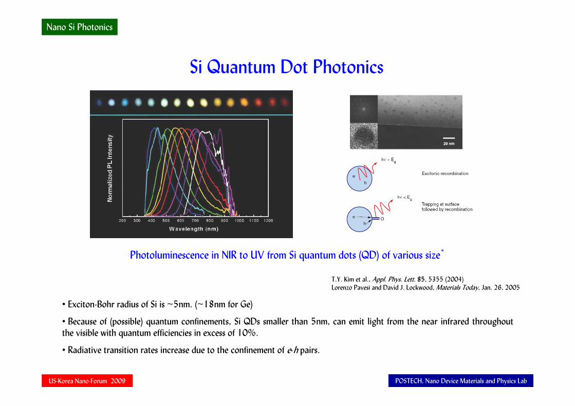
Si Quantum Dot Photonics
• Exciton-Bohr radius of Si is ~5nm. (~18nm for Ge)
• Because of (possible) quantum confinements, Si QDs smaller than 5nm, can emit light from the near infrared throughout the visible with quantum efficiencies in excess of 10%.
• Radiative transition rates increase due to the confinement of e-h pairs.
Photoluminescence in NIR to UV from Si quantum dots (QD) of various size*
T.Y. Kim et al., Appl. Phys. Lett. 85, 5355 (2004)Lorenzo Pavesi and David J. Lockwood, Materials Today, Jan. 26, 2005
Nano Si Photonics

US-Korea Nano-Forum 2009 POSTECH, Nano Device Materials and Physics Lab
Nano Silicon Photovoltaics
Multiple Exciton Generation in Si Quantum Dots
M.C. Beard, Nano. Lett. 7, 2506 (2007)
• Multiple bound e-h pairs (excitons) can be generated in Si nanocrystals (9.5 nm) upon photon absorption of energy greater than twice the band gap.
• The exciton production quantum was found to be 2.6 excitons per absorbed photon at 3.4Eg.
US-Korea Nano-Forum 2009 POSTECH, Nano Device Materials and Physics Lab
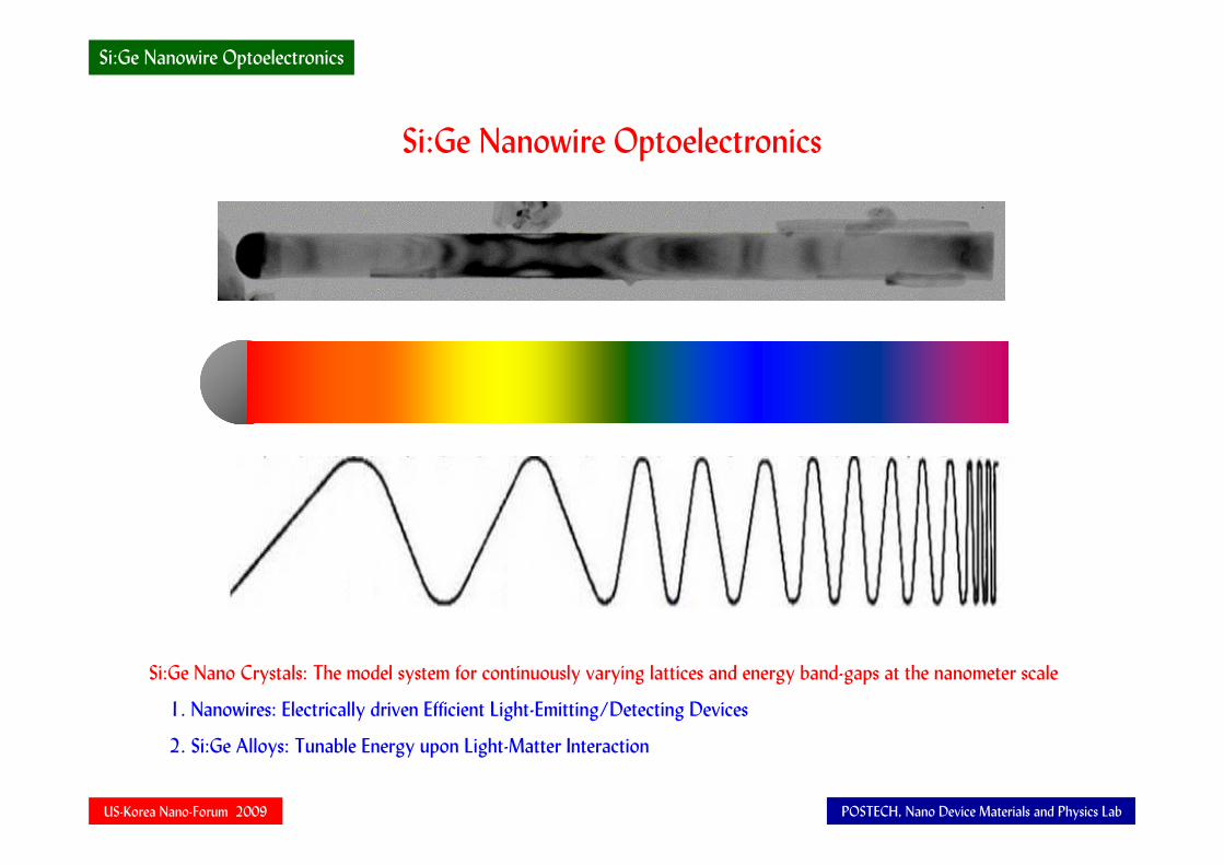
Si:Ge Nanowire Optoelectronics
Si:Ge Nano Crystals: The model system for continuously varying lattices and energy band-gaps at the nanometer scale
1. Nanowires: Electrically driven Efficient Light-Emitting/Detecting Devices
2. Si:Ge Alloys: Tunable Energy upon Light-Matter Interaction
Si:Ge Nanowire Optoelectronics

US-Korea Nano-Forum 2009 POSTECH, Nano Device Materials and Physics Lab
Vapor-Liquid-Solid (VLS) Nanowire Growth
• Catalyst-assisted CVD of group IV semiconductor nanowires: - Sources: SiH4 and GeH4- Dopants: PH3 and B2H6
(Liquid)
(Solid)SiH4, GeH4
2H2
Si
(Vapor)
Conventional VLS-CVD Nanowire Growth
Growth of Single-Crystalline Si1-xGex Nanowires
2μm 5nm
Chang-Beom Jin et al., Appl. Phys. Lett. 88, 193105 (2006)Jee-Eun Yang, et al., Nano Lett. 6, 2679 (2006)

US-Korea Nano-Forum 2009 POSTECH, Nano Device Materials and Physics Lab
Si1-xGex Nanowire Crystals: Optical Band-Edge Absorption
Band-Gap Modulation in Si1-xGex Nanowires
• The optical band-edge of 0.68eV and 1.05eV for Ge and Si nanowires, and these values agree with the energy band-gaps of bulk Ge and Si crystals of 0.65eV and 1.12eV.
• The optical band-edge in various Si1-xGex nanowires systematically shifts from that of Si nanowires to that of Ge nanowires with increasing Ge content.
• We observed strong blue-shift of optical band-edge for thinner nanowires whose diameter is smaller than 10nm. (Exciton-Bohr radius of 4.7nm for Si and 17.7nm for Ge)
Jee-Eun Yang et al., Nano Lett. 6, 2679 (2006)

US-Korea Nano-Forum 2009 POSTECH, Nano Device Materials and Physics Lab
Spatially Resolved Optoelectronic Measurements
532 nm Laser
Diffraction limit :.. AN
kR λ×=Δ
k : technical constant (~0.61)N. A. : numerical aperture (0.5, 0.9)
= 360 nm, 650 nm
• A new experimental setup based on a scanned laser confocal microscope allows combined measurements of “spatially resolved” electroluminescence and photoconductivity.
• The setup also allows the “spectral measurements” of electroluminescence and correlated photon counting.
• With the addition of an ultrafast laser, it should also allow “time-resolved measurements”.
Nano Optoelectronics Laboratory

US-Korea Nano-Forum 2009 POSTECH, Nano Device Materials and Physics Lab
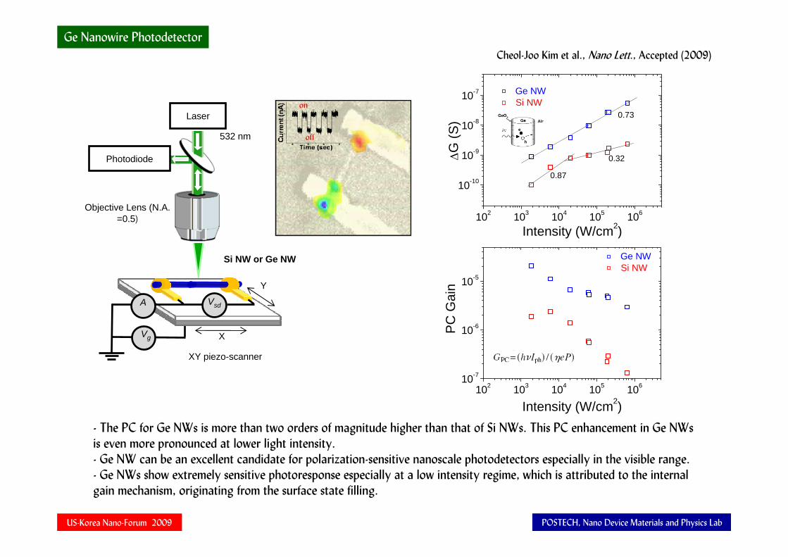
Cheol-Joo Kim et al., Nano Lett., Accepted (2009)
Intra-Nanowire p-n diode
Photocurrent in Si Nanowire p-n diode
-300
D S
n p
Vsd = -5.0 V
Vsd = -2.5 V
Vsd = 0.0 V
Vsd = 2.5 V
Vsd = 5.0 V
nA
0
100
hνe
h
Drain Source
2um
n
p
Vb

US-Korea Nano-Forum 2009 POSTECH, Nano Device Materials and Physics Lab
Confocal Raman Spectro-Microscopy
Raman Scattering in Si1-xGex Semiconductors
Jee-Eun Yang et al., Appl. Phys. Lett., 92, 263111 (2008)(with Prof. Zee Hwan Kim, Korea Univ. )
US-Korea Nano-Forum 2009 POSTECH, Nano Device Materials and Physics Lab
- The PC for Ge NWs is more than two orders of magnitude higher than that of Si NWs. This PC enhancement in Ge NWsis even more pronounced at lower light intensity.- Ge NW can be an excellent candidate for polarization-sensitive nanoscale photodetectors especially in the visible range. - Ge NWs show extremely sensitive photoresponse especially at a low intensity regime, which is attributed to the internal gain mechanism, originating from the surface state filling.
Ge Nanowire Photodetector
102 103 104 105 106
10-10
10-9
10-8
10-7
0.32
0.87
ΔG
(S)
Intensity (W/cm2)
Ge NW Si NW
0.73
102 103 104 105 10610-7
10-6
10-5
PC
Gai
n
Intensity (W/cm2)
Ge NW Si NW
Photodiode
532 nm
XY piezo-scanner
A Vsd
Objective Lens (N.A. =0.5)
Laser
X
Y
Vg
Si NW or Ge NW
Cheol-Joo Kim et al., Nano Lett., Accepted (2009)

US-Korea Nano-Forum 2009 POSTECH, Nano Device Materials and Physics Lab
10 μm
NanowireSubstrate
50 nm 2 nm
(a) (b) (c)
20 μm
Vertical Growth by Epitaxy on (111) Si Substrates
Cheol-Joo Kim et al., Appl. Phys. Lett., In Press (2009)Kibum Kang et al., Adv. Mater. 20 4684 (2008)
Epitaxial NW Growth for Ordered Arrays

US-Korea Nano-Forum 2009 POSTECH, Nano Device Materials and Physics Lab
Substrate: SiO2(100 nm)/Si(111)-p
Metal deposition& PS lift-off
SiO2 Dry & Wet etching
Au deposition& Lift-offGrowth of Si NWs
Reactive ion etching
Si(111) SiO2 Metal
PS Au
Epitaxial NW Growth for Ordered Arrays
(I) PS Nanosphere Lithography

US-Korea Nano-Forum 2009 POSTECH, Nano Device Materials and Physics Lab
Si Nanowire Arrays from Au-Catalyst Patterns by Nanosphere Lithography
Templated-Assisted NW Growth for Ordered Arrays
US-Korea Nano-Forum 2009 POSTECH, Nano Device Materials and Physics Lab
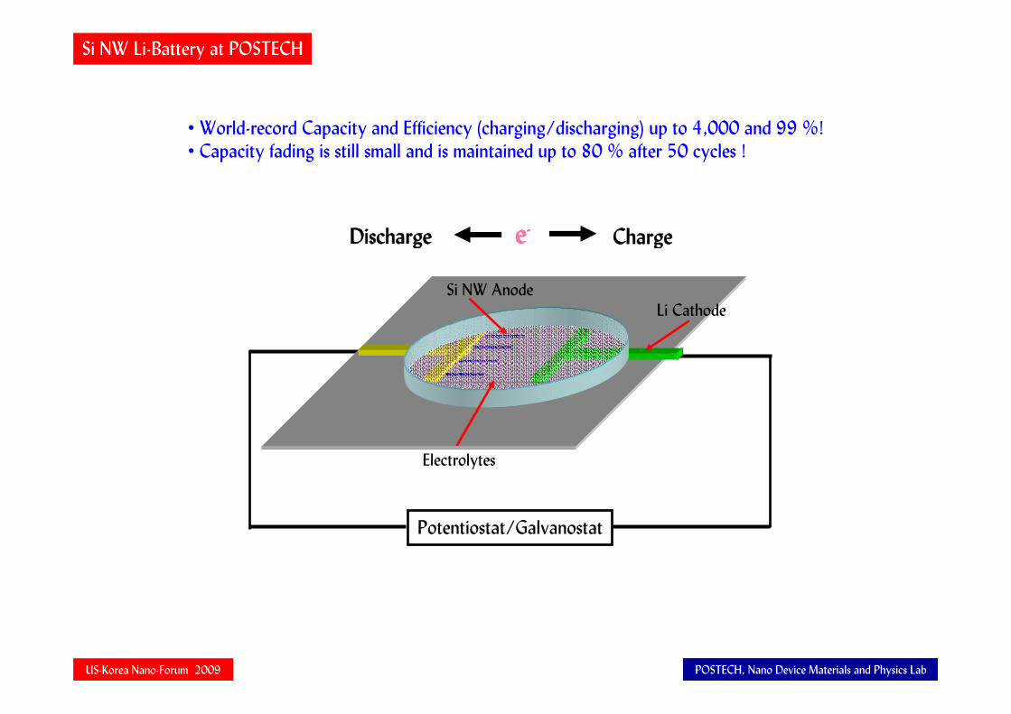
(1) Si nanowire vs. NiSi nanowireSi NW Li-Battery at POSTECH
• World-record Capacity and Efficiency (charging/discharging) up to 4,000 and 99 %!• Capacity fading is still small and is maintained up to 80 % after 50 cycles !
AnodeLOAD
e- ChargeDischarge
Potentiostat/Galvanostat
Si NW Anode Li Cathode
Electrolytes

US-Korea Nano-Forum 2009 POSTECH, Nano Device Materials and Physics Lab
NNANOANO DDEVICE EVICE MMATERIALSATERIALS & Physics L& Physics LABAB
Jee-Eun Yang Hyun-Seung Lee Cheol-Joo Kim Kibum Kang