Water, Land, and Air; Landforms Simrin Khan, Ariel Rocio, Michael Chung.

I
Group 10
Muhammed Ali Khan Michael Gannon Michael Peffers Ahmad Buleybel

II
Sponsored by
Director of the University of Central Florida Sustainability & Energy Management:
Mr. David Norvell
In collaboration with
Industrial Engineering Team Amanda Longman
Joshua MacNaughton Andrew Wolodkiewicz
Mechanical Engineering Team
Daniel Gould
Connie Griesemer
Ryan Lewis
Jonathan Torres
Ryan Tribbey

I
TABLE OF CONTENTS EXECUTIVE SUMMARY: ........................................................................................................ 1
1.2 MOTIVATION: ..................................................................................................................... 2
1.2.1 UCF GOING GREEN: .................................................................................................... 2
1.2.2 ENVIRONMENTAL BENEFITS: ................................................................................... 2
1.3 GOALS AND OBJECTS: ................................................................................................... 2
1.3.1 MONITORING: ................................................................................................................ 2
1.3.2 Energy Output (Power): ................................................................................................. 3
1.4 SPECS & BUDGET PROJECTION: ................................................................................ 3
1.5 DIVISION OF LABOR: ....................................................................................................... 4
1.6 PROGRAMMING AND CODE DIVISION: ...................................................................... 6
1.7 PROJECT BLOCK DIAGRAM: ......................................................................................... 7
1.8 TIMELINES:......................................................................................................................... 8
1.9 MILESTONES: .................................................................................................................... 8
1.10 SCOPE OF WORK: ......................................................................................................... 9
1.11 ALLOCATED AREA: ...................................................................................................... 10
1.12 ANGLE OF SOLAR PANELS: ...................................................................................... 10
1.13 AVAILABLE SPACE: ..................................................................................................... 12
1.14 DESIGN AND PROJECTED BUDGET: ...................................................................... 13
1.15 RISKS: ............................................................................................................................. 15
CHAPTER 2: RESEARCH ................................................................................................... 15
2.1 SOLAR PANELS: ............................................................................................................. 15
2.1.1 MONOCRYSTALLINE SOLAR PANELS: ................................................................. 15
2.1.2 POLYCRYSTALLINE SOLAR PANELS: ................................................................... 16
2.1.3 THIN FILM TECHNOLOGY: ........................................................................................ 17
2.1.4 IBM SOLAR CELL: ....................................................................................................... 18
2.1.5 ORGANIC SOLAR CELLS: ......................................................................................... 18
2.1.6 SOLAR RADIATION: .................................................................................................... 18
2.1.7 TEMPERATURE EFFECT: ......................................................................................... 19
2.1.8 SOLAR PANEL SUMMARY: ....................................................................................... 20
2.2 INVERTERS: ..................................................................................................................... 21

II
2.2.1 OFF-GRID INVERTERS: ............................................................................................. 21
2.2.2 GRID-TIE INVERTERS: ............................................................................................... 22
2.2.3 INVERTER FEATURES: .............................................................................................. 23
2.2.4 MODIFIED SINE WAVE INVERTERS: ...................................................................... 23
2.2.5 PURE SINE WAVE INVERTERS: .............................................................................. 23
2.2.6 INVERTER PRICE, QUALITY AND SIZE: ................................................................ 24
2.2.7 CHOSEN INVERTER: .................................................................................................. 25
2.2.8 FRONIUS IG 3000: ....................................................................................................... 25
2.3 COMBINER BOX: ............................................................................................................. 26
2.4 SURGE ARRESTOR: ...................................................................................................... 29
2.5 WIRES AND CONNECTORS:........................................................................................ 30
2.6 WIRELESS TECHNOLOGY: .......................................................................................... 31
2.6.1 WIFI TECHNOLOGY: ................................................................................................... 32
2.6.1a: 802.11a: ...................................................................................................................... 32
2.6.1b: 802.11b: ...................................................................................................................... 32
2.6.1c: 802.11g: ....................................................................................................................... 32
2.6.1d: 802.11n: ...................................................................................................................... 33
2.6.2 INFRARED: .................................................................................................................... 34
2.6.3 BLUETOOTH TECHNOLOGY: ................................................................................... 35
2.6.4 ZIGBEE TECHNOLOGY: ............................................................................................. 37
2.7 WIRE TRANSMITTION TECHNOLOGY: ..................................................................... 38
2.7.1 DIRECT WIRE COMMUNICATION: .......................................................................... 38
2.7.2 POWER LINE COMMUNICATION: ............................................................................ 39
2.8 WIRELESS VS WIRED TECHNOLOGY: ..................................................................... 40
2.8.1 WIRES: ........................................................................................................................... 40
2.8.2 WIRELESS: .................................................................................................................... 41
2.9 ANALOG VS DIGITAL: .................................................................................................... 42
2.9.1 ANALOG SIGNAL: ........................................................................................................ 42
2.9.2 DIGITAL SIGNAL: ......................................................................................................... 43
2.10 BATTERIES: ................................................................................................................... 44
2.10.1 NICKEL-CADMIUM: ................................................................................................... 45
2.10.2 NICKEL METAL HYDRIDE: ...................................................................................... 46
III
2.10.3 SEALED LEAD: ........................................................................................................... 47
2.10.4 LITHIUM ION BATTERIES: ....................................................................................... 49
2.11 MOUNTING SYSTEM: .................................................................................................. 50
2.11.1 TRACKING THE SUN: ............................................................................................... 50
2.11.1a Sun Light Sensor: ..................................................................................................... 50
2.11.1b Preprogrammed angles Tracking System: ........................................................... 51
2.11.1c PHOTORESISTORS: ............................................................................................... 51
2.11.1D IR CAMERA: ............................................................................................................. 52
2.11.2 ACTUATION OR NON-ACTUATION: ...................................................................... 52
2.11.2a ACTUATION: ............................................................................................................. 53
2.11.2b NON-ACTUATION: ................................................................................................... 55
2.11.3 MOUNTING SYSTEM DESIGNED BY MECHANICAL ENGINGEERS ............. 56
2.12 FPGA VS MICROCONTROLLER: .............................................................................. 58
2.12.1 FPGA CHIP:................................................................................................................. 58
2.12.2 MICROCONTROLLER CHIP: ................................................................................... 59
CHAPTER 3: DESIGN ........................................................................................................... 60
3.1: OVERALL DESIGN DECISIONS: ................................................................................. 60
3.2 MONITORING SYSTEM DESIGN: ................................................................................ 65
3.2.1 VOLTAGE SENSORS: ................................................................................................. 66
3.2.1.a VOLTAGE SENSING: ............................................................................................... 66
3.2.2 RESISTORS: ................................................................................................................. 67
3.2.2a CARBON COMPOSITE RESISTORS: .................................................................... 68
3.2.2b CARBON FILM RESISTORS: ................................................................................... 69
3.2.2c Wire Wound Resistors: ............................................................................................... 70
3.2.3 VOLTAGE DIVIDER/RESISTOR ................................................................................ 71
CONCLUSION: ........................................................................................................................ 71
3.3 ZENER DIODES: .............................................................................................................. 72
3.4 OPERATION AMPLIFIERS: ........................................................................................... 73
3.5 CURRENT SENSORS: ................................................................................................... 75
3.5.1 ACS712 CURRENT SENSOR: ................................................................................... 75
3.5.2 CR5410-20 CURRENT SENSOR: ............................................................................. 76
3.5.3 CSLT6B100 CURRENT SENSOR: ............................................................................ 77

IV
3.6 TEMPERATURE SENSOR:............................................................................................ 79
3.6.1 WE710 TEMPERATURE SENSOR: .......................................................................... 80
3.6.2 CS220 TEMPERATURE SENSOR: ........................................................................... 80
3.6.3 SA1-RTD TEMPERATURE SENSOR: ...................................................................... 81
3.7 DATA ACQUISITION: ...................................................................................................... 81
3.7.1 RJ45 CABLE/CONNECTION: ..................................................................................... 82
3.8 WIRELESS: ....................................................................................................................... 83
3.9 TERMINAL BLOCK: ......................................................................................................... 83
3.10 MULTIPLEXERS: ........................................................................................................... 85
3.10.1 MC14067B ANALOG MULTIPLEXER: .................................................................... 86
3.10.2 AS250A ANALOG MULTIPLEXER: ......................................................................... 87
3.10.3 MPC506A ANALOG MULTIPLEXER: ..................................................................... 87
3.11 MICROCONTROLLERS: .............................................................................................. 89
3.11.1 ANALOG TO DIGITAL I/O PINS: ............................................................................. 89
3.12 DEVELOPMENT KIT: .................................................................................................... 91
3.12 SURFACE MOUNT OR THROUGH HOLE: .............................................................. 92
3.13 NUMBER OF BITS OF ACCURACY: ......................................................................... 93
3.14 OPERATING TEMPERATURE: ................................................................................... 94
3.15 POWER SUPPLY: ......................................................................................................... 94
3.15.1 POWER SUPPLY DESIGN: ...................................................................................... 94
3.16 BASE STATION: ............................................................................................................ 95
3.16.1 RECEIVER: .................................................................................................................. 95
3.16.2 CONFIGURE: ............................................................................................................ 100
3.16.3 TRANSMITTER: ........................................................................................................ 100
3.16.7 ADDRESSING: .......................................................................................................... 103
3.16.8 XBEE‟S MODES OF OPERATION: ....................................................................... 104
3.16.9 BASE STATION SOFTWARE: ............................................................................... 105
CHAPTER 4: TESTING: ...................................................................................................... 106
4.1 INVERTER TEST: .......................................................................................................... 106
4.2 MICROCONTROLLER AND PCB TEST: ................................................................... 107
4.3 COMPONENT TESTING: ............................................................................................. 109
4.4 WIRELESS CONNECTIVITY TROUBLESHOOT: .................................................... 110

V
4.5 WATER RESISTIVITY: .................................................................................................. 111
4.6 WIND AFFECT: .............................................................................................................. 112
4.7 TEMPERATURE TESTING: ......................................................................................... 113
4.8 CLOUDS AND SHADE AFFECT: ................................................................................ 113
4.9 DUST AND DIRT TEST: ............................................................................................... 114
4. 10 HUMIDITY TEST: ........................................................................................................ 114
CHAPTER 5: PREVIOUS WORKS: ................................................................................... 114
5.1 SOLAR SYSTEM/MONITORING SYSTEM: .............................................................. 114
5.1.1 SOLAR PANEL MONITOR SYSTEM: ..................................................................... 114
5.1.2 SOLAR ARRAY MONITOR: ...................................................................................... 115
CHAPTER 6: PROJECT BUDGET: ................................................................................... 116
6.1 BUDGET PROJECTION: .............................................................................................. 116
6.2 TOTAL ARRAY COST: .................................................................................................. 118
6.3 ASSESSMENT: .............................................................................................................. 119
CHAPTER 7: CONCLUSION .............................................................................................. 119
7.1CONCLUSION: ................................................................................................................ 119
BIBLIOGRAPHY:................................................................................................................... 121
APENDIES: PERMISSIONS ............................................................................................... 122
PERMISSIONS RECEIVED: ............................................................................................... 122
PREMISSION PENDING ..................................................................................................... 125

1
CHAPTER 1
EXECUTIVE SUMMARY:
As fresh Engineers, we are looking to provide solutions to the energy supply in a green manner. And a great way of doing that is using natural resources, mainly using PVC also known as Photovoltaic Cell or Solar Cell. The idea is to create a solar farm within the property of the UCF campus so we can cut down the energy cost. A solar farm is just like any other farm, except it doesn‟t grow fruits and vegetables and does not need irrigation. However, it does need sunlight to produce desired results. For our senior design project we are only going to consider one array since building a PVC farm is not feasible. An array of solar panels will be installed on campus. The array will consist of 12 solar panels. The installation and connection of the panels will be done at the field reserved for the future PVC farm. Mounting will be done with the help of mechanical engineers. All the panels will be connected in series connection. The most important part of our project is the panel monitoring. Each panel would be connected to a voltage, current, and temperature sensor determining the output voltage, current, and temp. from each panel. The sensors will then send the data to a microcontroller. Microcontroller will send the data a wireless component and finally the wireless component will communicate with our base computer to display the data. This will allow us to monitor each panel output voltage, current and power individually. For example, if panel X is producing only 100 volts and it is supposed to produce 150 volts, by wireless computer monitoring, we will know it is panel X that is malfunctioning and needs maintenance. We can then approach the problem directly for maintenance or troubleshooting. The solar panels when exposed to sunlight generate DC electricity, while there are some appliances available that will run directly from DC, most appliances require AC. In order to switch the current type, we will need a Power Inverter. The inverter will be connected to solar panels to provide the conversion before reaching into the power grid. Once the inverter is connected to the grid, we can start taking advantage of the renewable energy. The grid is responsible for supplying AC electricity to the power outlets in households. So, this renewable energy will be supplementing the power supplied by the power company, hence, reducing the amount of purchasing of energy from power companies. We will not be storing any energy or charge batteries for later use as our peak power consumption timing matches with the timing of peak solar energy. All the power generated will be used completely on daily basis. This project is not intended for UCF to be completely independent and self sufficient of energy. The idea behind this project is to cut UCF‟s electricity costs. We still need to have energy providers since solar farm will only be producing a fraction of energy during rainy days.

2
1.2 MOTIVATION:
1.2.1 UCF GOING GREEN: There are multiple things that motivate our team on this project. For one every member on the team wanted to be a part of a project that would challenge us, and make an impact in the real world. It was that the Mr. Norvell presented his power point presentation, challenging a group to design a solar array with panel by panel monitoring. This project offers us multiple benefits as engineers. Firstly it allows us to work hand in hand with industrial, mechanical, and a client. This is preparing us with real world experience on a team orientated environment. Second this project offers the opportunity to research, design, and develop our own independent circuit board, another part of real world experience. Lastly this project allows us as engineers to help UCF accomplish its goal of being 100% neutral by the year 2050. With this project Mr. Norvell is aiming to one day alleviate UCF of 12 - 15% of its energy consumption from the grid. Our team is also motivated with the knowledge that is design well and built correctly UCF will invest in building a 3 Megawatt photovoltaic field. Using our design to build this photovoltaic field would add a great resume piece to every team member involved.
1.2.2 ENVIRONMENTAL BENEFITS: Another huge motivational tool for our group is the enormous environmental benefit from the project. After burning fossil fuels for hundreds of years and leaving a large carbon footprint many private organizations, government organizations, and even individuals are looking towards cleaner power. With everything in the US turnings its attention to “going green” renewable energy sources like solar energy is becoming more and more popular. With growing concerns on the depletion of the ozone layer and the green house effect there has never been a more urgent time to look into renewable energy sources. It is our ambition as a group to join this “green”, earth-saving movement that drives us on this project as young and fresh engineers. The time for changing the world is now, and as up and coming engineers the responsibility is ours.
1.3 GOALS AND OBJECTS:
1.3.1 MONITORING: For this project our team has many objectives and goals. The objective of this project to design and build a 3 kilo-watt 12 panel photovoltaic array that will serve as the prototype for arrays that will one day make up a 3 mega-watt photovoltaic farm. A secondary objective for this project to is build a independent panel by

3
panel monitoring system. To complete this monitoring systems many goals were set. First we would have to design a circuit board from the ground up that will take in three different variables. Once the variable are collected they will be converted from analog to digital then sent wirelessly to a web based computer. From this the data will be available anywhere it is needed. The three variables selected to be monitored from each panel was the panel‟s voltage, current, and temperature. This panel by panel monitoring system has many advantages for the client. First they can monitor their photovoltaic farm from anywhere with internet. Secondly they can not only determine when the array or farm is not performing like expected, but they can determine the exact panels not performing and perform the adequate maintenance. This not only allows the client to keep their farm running at full power, it takes a lot of the stress, money, and time out of troubleshooting the system when performance is below 100%.
1.3.2 Energy Output (Power): After designing the monitoring system a secondary objective of the project was to develop an array that would allow the client to multiply until desired energy output was reached. With UCF looking to build a 3 mega-watt photovoltaic farm our team set a goal of reaching a total of 3 kilo-watts of power out of our single array. This will allow us to present UCF with a design worth using when the 3 mega-watt photovoltaic farm is built.
1.4 SPECS & BUDGET PROJECTION:
12 - 240W Monocrystalline panels
Panels will be connected in series
Mounted at a 28 degree angle
37.4V Open Circuit Voltage, 30.1V Maximum Power Voltage
8.65A Short Circuit Current, 7.98 Maximum Power Current
Panel Dimensions: 39.1” Wide, 64.6” Tall, 1.8” Thick
Weight: 44.1lbs/ 20.0 kg
Operating Temperature -40 to 194 degrees F
1 – Fronius IG 4000 Inverter
Recommended PV power 3000-5000 Wp
Max. DC Input Voltage 500V, Operating DC Voltage 150-450V
Max. usable DC input current 26.1A
Inverter Dimensions: 16.5” Wide, 28.4” Long, 8.8” high
Weight: 42lbs/ 19kgs
Operating Temperature: -5 to 122 degrees F
12 – Small circuit boards collecting voltage, current, and temp from each panel.
1 – Main circuit board collecting the data once a minute from smaller boards using a PIC18F series microcontroller with at least 3 I/O pins.

4
1 – wireless device able to transmit data 800 yards
3 – 16:1 Multiplexers
Solar panels will be no more than $10,000
Circuit board design and construction will be no more than $800
Mounting system will be no more then $1000
Inverter will be no more then $4000
The specifications and requirements above are tentative, as the project progresses we might adjust them. The adjustments will be based on hardware limitations and cost vs. efficiency considerations. After building and testing the system we will have a better idea on budget assessments, and parts used.
1.5 DIVISION OF LABOR: Our team consists of four members, all electrical engineers. After a detailed team discussion, we improvised the chart in Figure 1 that shows the breakdown of the amount of work involved in the project. Each member is responsible for their individual tasks as well as to let the group know any important details that could affect other group member‟s tasks. Even though each member is responsible for their own specific task, we have weekly meetings to discuss what one has achieved so far and teach all the group members about their learning of their part of the project. In this case, all the members will be equally knowledgeable about the project however, only one member will specialize in the details and specifications of each part. So when the prototyping begins, we will assign the right member for the specific part of the project. Figure 1 merely represents the specialties each member is expected to achieve at the end of the senior design I. Ahmad‟s main responsibilities:
To define the connectivity between the panels
Define the functionality and need of current, voltage and temp. sensors
Research for the most economical solar panels
Research for suitable current, temperature and voltage sensors
Design the panel connection
Help in design the schematics of the circuit board Ali‟s main responsibilities:
Define the function of an inverter
Define the wireless connection and benefits of wireless connectivity
Research the best wireless device to connect solar panels to a microcontroller
Communication between the microcontroller and the base station
Help in designing of the schematics
Making sure the PCB is in good shape
Test all the wireless connections

5
Mike P.‟s main responsibilities:
Define the functionality of a microcontroller in collaboration with Ali
Assist Ahmad to define the functions of sensors
Research various microcontrollers and their programming language
Look for various schematics of the connections of the microcontrollers
Solder all the sensors and components which are not done by the PCB vendor
Test the PCB for any potential damage Mike G.‟s main responsibilities:
Define the goals of the project
Describe the motivations to pick this project as our senior design
Define the goals and outcome of the project
Research for the architecture of the system
Analyze previous similar projects
Analyze the data sheet of previous projects
Help is design the schematics of the circuit
Help in conducting the test and compare the data with previous projects
Responsible for data screening including display and script for the display
Figure 1.5-1: Roles and Responsibilities
6
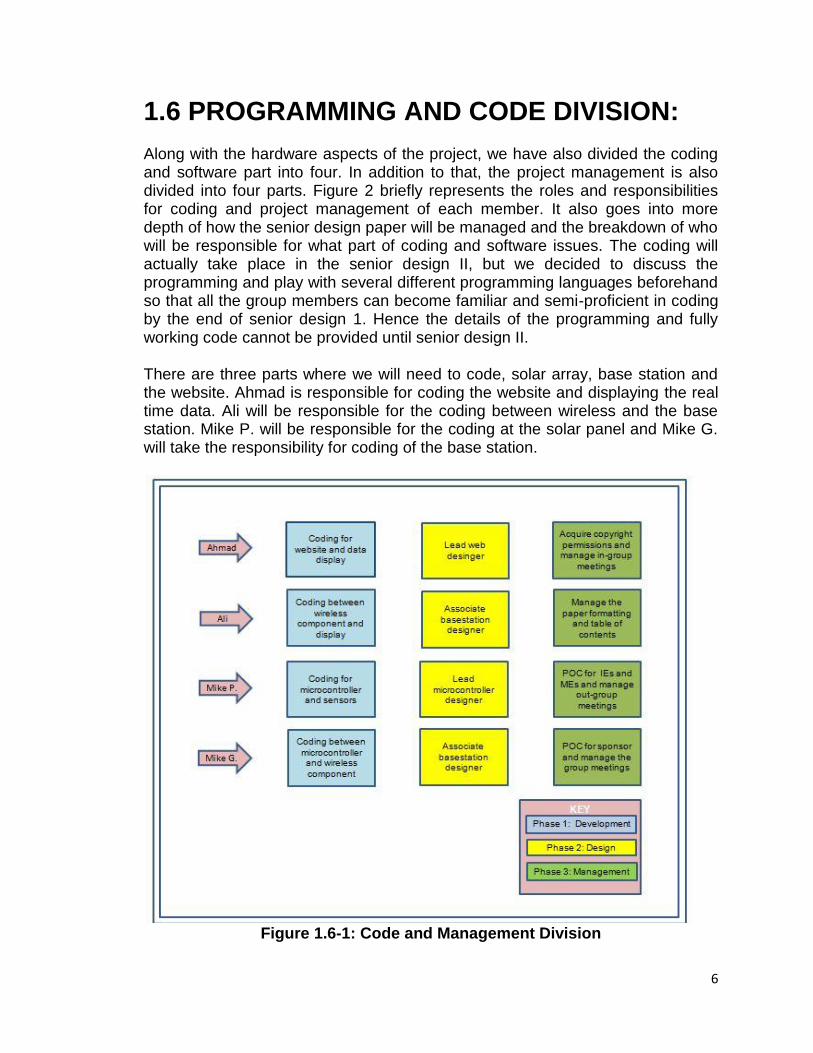
1.6 PROGRAMMING AND CODE DIVISION: Along with the hardware aspects of the project, we have also divided the coding and software part into four. In addition to that, the project management is also divided into four parts. Figure 2 briefly represents the roles and responsibilities for coding and project management of each member. It also goes into more depth of how the senior design paper will be managed and the breakdown of who will be responsible for what part of coding and software issues. The coding will actually take place in the senior design II, but we decided to discuss the programming and play with several different programming languages beforehand so that all the group members can become familiar and semi-proficient in coding by the end of senior design 1. Hence the details of the programming and fully working code cannot be provided until senior design II. There are three parts where we will need to code, solar array, base station and the website. Ahmad is responsible for coding the website and displaying the real time data. Ali will be responsible for the coding between wireless and the base station. Mike P. will be responsible for the coding at the solar panel and Mike G. will take the responsibility for coding of the base station.
Figure 1.6-1: Code and Management Division

7
1.7 PROJECT BLOCK DIAGRAM: We already have a flowchart developed for our project which represents main components of the project. Figure 3 shows the block diagram of our project which basically shows the two major portions of our project, the Base Station and the Solar Cell station. These two parts are the main objectives of the project.
Figure 1.7-1: Flowchart/Block Diagram of the Project
8
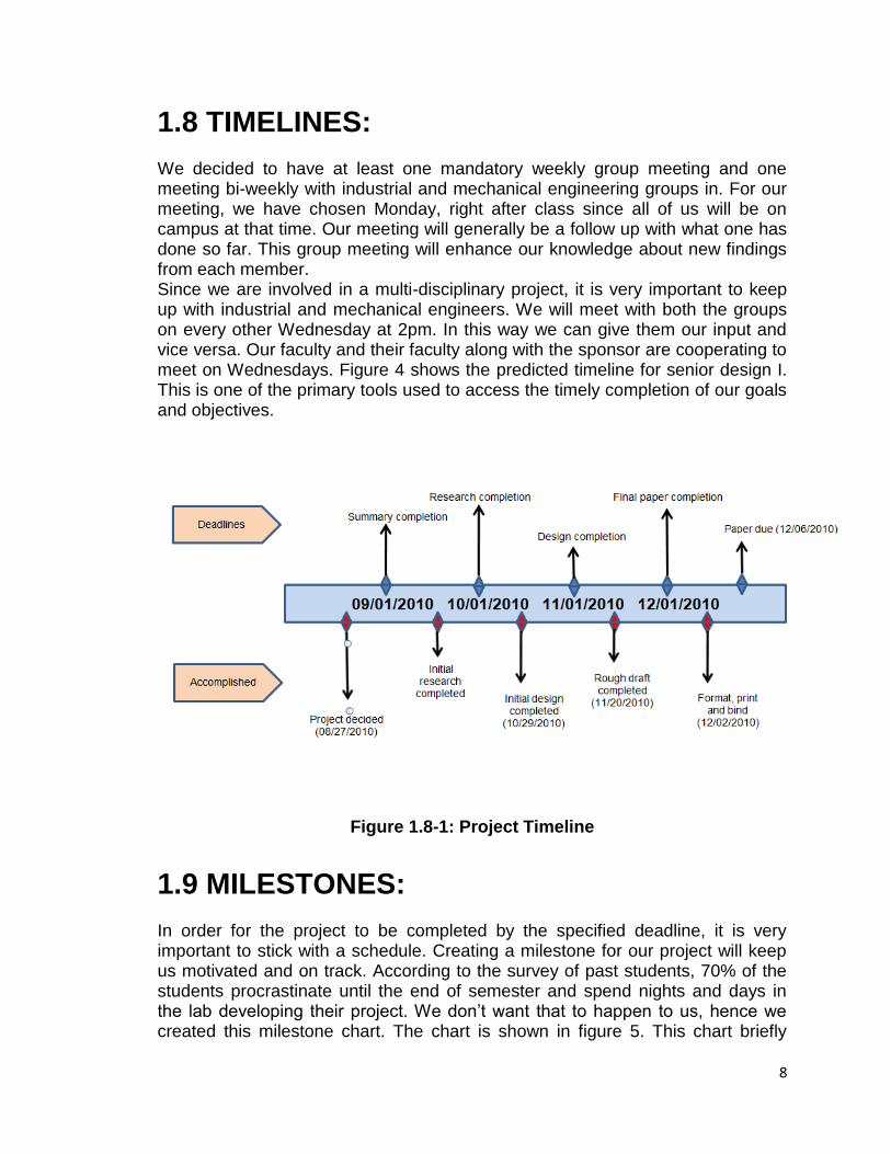
1.8 TIMELINES: We decided to have at least one mandatory weekly group meeting and one meeting bi-weekly with industrial and mechanical engineering groups in. For our meeting, we have chosen Monday, right after class since all of us will be on campus at that time. Our meeting will generally be a follow up with what one has done so far. This group meeting will enhance our knowledge about new findings from each member. Since we are involved in a multi-disciplinary project, it is very important to keep up with industrial and mechanical engineers. We will meet with both the groups on every other Wednesday at 2pm. In this way we can give them our input and vice versa. Our faculty and their faculty along with the sponsor are cooperating to meet on Wednesdays. Figure 4 shows the predicted timeline for senior design I. This is one of the primary tools used to access the timely completion of our goals and objectives.
Figure 1.8-1: Project Timeline
1.9 MILESTONES: In order for the project to be completed by the specified deadline, it is very important to stick with a schedule. Creating a milestone for our project will keep us motivated and on track. According to the survey of past students, 70% of the students procrastinate until the end of semester and spend nights and days in the lab developing their project. We don‟t want that to happen to us, hence we created this milestone chart. The chart is shown in figure 5. This chart briefly

9
explains the distribution of work throughout senior design I and II. There are particular tasks that will be exclusive to each semester and some of them will be done in both the semesters.
Figure 1.9-1: Milestone Chart
1.10 SCOPE OF WORK:
The scope of work for the Electrical Engineering team includes one set of tasks that correspond to EE-only work and a second set of tasks which combines the design creativities of all three teams: the electrical engineers, the industrial engineers and the mechanical engineers. As explained in the figure 5, some of the tasks for our group will be completed in the remainder of the fall semester and eventually will go to the spring semester. Then the project will use the break between semesters as a natural point at which to transition into the tasks
10
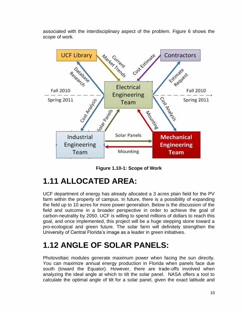
associated with the interdisciplinary aspect of the problem. Figure 6 shows the scope of work.
Figure 1.10-1: Scope of Work
1.11 ALLOCATED AREA: UCF department of energy has already allocated a 3 acres plain field for the PV farm within the property of campus. In future, there is a possibility of expanding the field up to 10 acres for more power generation. Below is the discussion of the field and outcome in a broader perspective in order to achieve the goal of carbon-neutrality by 2050. UCF is willing to spend millions of dollars to reach this goal, and once implemented, this project will be a huge stepping stone toward a pro-ecological and green future. The solar farm will definitely strengthen the University of Central Florida‟s image as a leader in green initiatives.
1.12 ANGLE OF SOLAR PANELS: Photovoltaic modules generate maximum power when facing the sun directly. You can maximize annual energy production in Florida when panels face due south (toward the Equator). However, there are trade-offs involved when analyzing the ideal angle at which to tilt the solar panel. NASA offers a tool to calculate the optimal angle of tilt for a solar panel, given the exact latitude and

11
longitude of a given location on Earth [1]. The exact coordinates of the three-acre field were found using a website recommended by the NASA website. See Figure 1.7.1.2. A screenshot of the location is included in Figure 1.7.1.1. The summary table for panel tilt angle from NASA‟s tool is shown in Figure 1.7.1.3.It shows that of the angles tested by NASA, a 28° tilt was optimal. This is the tilt used in the ME mounting design. The optimal tilt angles for each month are not used in the ME design because they opted for a fixed mounting system instead of one that changed tilt every month.
Figure 1.12-1: Coordinates of Solar Field http://itouchmap.com/latlong.html
Lat 28.591 Lnog-81.188
Jan Feb Mar Apr May Jun Jul Aug Sep Oct Nov Dec
OPTANG 51.0 42.0 29.0 14.0 1.0 0.0 0.0 7.0 22.0 38.0 49.0 53.0
Radiation Incident
4.58 4.88 5.37 5.91 6.24 5.53 5.43 5.09 4.76 4.95 4.81 4.52
Table 1.12-1: Optimal Angle and Monthly Averaged Radiation Incident from NASA

12
Lat 28.59
1 Lnog-81.18
8
Jan Feb Mar Apr May Jun Jul Aug Sep Oct Nov Dec Ann Avg
Tilt0 3.21
3.90
4.86
5.78 6.24 5.33 5.43 5.06 4.52 4.15 3.47 3.02 4.60
Tilt13 3.80
4.40
5.21
5.91 6.14 5.39 5.32 5.08 4.72 4.60 4.07 3.63 4.86
Tilt28 4.29
4.77
5.37
5.79 5.75 4.99 4.97 4.87 4.74 4.9 4.55 4.16 4.93
Tilt43 4.55
4.88
5.25
5.38 5.09 4.38 4.39 4.45 4.53 4.94 4.79 4.46 4.76
Tilt90 3.75
3.64
3.3 2.65 2.15 1.93 1.96 2.19 2.66 3.5 3.85 3.79 2.94
Table 1.12-2: Monthly Averaged Radiation Incident at Different Tilt Angles from NASA
1.13 AVAILABLE SPACE: The current space set aside for the farm amounts to just over 3 acres. The 3 acres were enough for 15 rows of 16 in-series arrays. This amounts to 2,880 panels mounted on 240 total arrays. Each array accommodates approximately 200 square feet (5‟ x 40‟) of field space. Five feet separate each row in order to prevent shadows from covering neighboring rows Figure1.7.2.1.
Figure 1.13-1: Current Space Each array‟s panels will face south (toward the Equator) with intention to maximize energy collection. When this configuration operates in favorable

13
conditions (clear skies, 75° F), it has a potential output of 691kW (0.691 MW). Rule of thumb in the solar industry is 1 MW for every 6 acres of panels (Robinson, Engineer, 2010). The total cost in panels amounts to $1,277,860. This field will also require a more powerful inverter; an inverter capable of handling 691 kW. Inverters of this size are an extreme cost for the project ranging from $300,000-$500,000. A 780 kW PV Powered commercial inverter at a cost of $331,250 is utilized in this design. Mounting cost remain the same per array. A smaller cost for prepping the land for construction of the farm also is added into the cost calculation. Crushed concrete is being brought in to cover the plot to minimize mowing and similar maintenance costs in the future. No additional labor costs are needed because it will be installed by the university.
1.14 DESIGN AND PROJECTED BUDGET: In collaboration with industrial engineers and mechanical engineers we projected a budget and overall design. Our client requests a 3 MW field. The same design used for the three-acre field can be replicated to produce a 3 MW field. The changes to focus on will be total number of arrays and increased inverter costs. It may be more practical to use an inverter that can handle more than one array, but larger inverters are more expensive. Clearing costs will also increase substantially as a result of having to clear a great amount of land. Previously, the farm was allocated to a field with mainly bush and brush clearing issues. More than likely, a 20-acre plot (needed to produce 3 MW) will contain numerous amounts of trees needed to be cut down and de-rooted. Having trees on land that needs to be cleared nearly doubles prepping and clearing costs due to the extra hours of labor required. Each job of this type is unique and requires an on-site estimate. In an interview with Dell Jones, Vice President of Regenesis Power in Estero, Florida, he talked about other costs involved in designing and constructing a large solar farm. He estimated that Regenesis Power would charge anywhere from 10-12 million dollars for a 3 MW system (Jones, 2010). This covers the design, materials and installation. It does not cover clearing and prepping the land. As shown in Table 6, the total cost analysis for the farm based on the prototype designed by the three engineering disciplines came out to be close to Dell‟s estimate, right around 13 million dollars.
Materials MEs Quantity Required Cost per unit($)
Total Cost($)
Solar Panels 14400 panels $612.00 $8,812,800.00
2" SCH40 304 Stainless Steel Pipe
144000 ft. $11.85 $1,706,400.00
U-Bolts (2.375" clearance)
60000 U-bolts $1.97 $118,200.00
Kee-Klamps (elbow connectors)
4800 elbows $24.24 $116,352.00

14
Kee-Klamps (t-connectors)
4800 t-conns $29.16 $139,968.00
Total Concrete Needed 4800 bags $2.98 $14,304.00
Materials EEs
Monitoring System 1040 system $800.00 $832,000.00
PowerGate Plus 500kW 480/3
6 inverter $151,393.00 $908,358.00
Connecting Wires & Grounding
75 connection $700.00 $52,500.00
Construction Costs
Clearing/Prepping Plot 15 Acres $3,000.00 $45,000.00
Crushed Concrete 15 Acres $2,645.00 $39,675.00
Total
Cost($) $12,785,557.00
Table 1.14-1: Costs associated with design for 3 MW
From the previous analysis of the field just over three acres, the power output was predicted to be no greater than 0.6 - 0.7 MW. Applying these numbers to the 3 MW field using an average of 0.6 MW for 3 acres, the field size would need to be around 15 acres. The maximum output of this proposed design is 3.3 MW coming from 1,200 arrays; 14,400 total panels. This output assumes maximum energy production from all panels. Although the numbers appear to provide the energy desired by the university, the panels also will lose 4 - 5% efficiency in summer months due to temperatures averaging at about 92° F. For every degree above 77° F, panel efficiency decrease by 0.5%. Ideal operating conditions are in clear skies at or below 77° F. High temperatures also decrease maximum power output of panels over time so it is appropriate to design the system to be just over 3 MW. Safety features included in the inverters will prevent any type of overload or damage in the case the field produces more energy than the inverters can handle (3 MW). The 3 MW design is cheaper per watt produced when compared to the 3-acre field as a result of a 500 kW inverter costing only $150,000 as opposed to the 3 acre field design in which a 780 kW inverter costs about $330,000. Commercial inverters are more limited in capacity options than smaller inverters such as the one purchased for the single array. This cost analysis assumes once again that the university will handle the installation of the entire farm. This cost analysis also fails to account for permit fees and tools required for installation.

15
1.15 RISKS: Inherent to photovoltaic panels, there is a risk that Florida‟s hot summer temperatures will reduce individual panel efficiency. The high temperatures are thought to make panel efficiencies deteriorate over time. Unexpected costs may arise with student installation of the solar farm. The client specified to the ME team that he desires the mounting system to be simple enough that student volunteer groups could perform the installation to save on labor costs. This idea has many inherent liabilities, including possible damage to the equipment by untrained student handlers. Other risks come from the location itself. Clearing costs for a 15 acre field are difficult to predict. The design was made without a concrete location in mind which may affect layout of panels leading to increased cost.
CHAPTER 2: RESEARCH
2.1 SOLAR PANELS:
2.1.1 MONOCRYSTALLINE SOLAR PANELS: Monocrystalline photovoltaic panels are the oldest and most common form of solar cell technology [2]. They offer the highest purity most efficient silicon wafers on the market. The high purity is due to the techniques used to manufacture monocrystalline solar cells, monocrystalline photovoltaic cells are made from a single crystal of silicon. This single cell composition is the reason that monocrystalline solar cells record the highest efficiency ratings in PV industry. The Efficiencies of monocrystalline solar panels range from 14-20 percent [2]. With the maximum module efficiency recorded at 22.7% [3]. Monocrystalline panel‟s high efficiency also has a hidden advantage. Less space is needed to produce the same kilowatts then other PV technologies. This is a huge advantage when you are trying to place a solar system on a roof where space is a major restriction. A third advantage to using monocrystalline solar panels is their longevity. Monocrystalline solar panels are one of the earliest types of photovoltaic cells produced and have proven over time to be very durable. The average monocrystalline solar panel system has a life-span of 25 years, with some lasting as long as 50 years depending on the conditions they are exposed to [2]. Another advantage to monocrystalline solar cells is there chemical makeup. All solar cells are design to take less dependency of fossil fuels monocrystalline solar cells take it a step further. Certain solar cells are made with a heavy medal called cadmium telluride, this particular kind of medal can be carcinogenic to humans [2]. If these solar panels containing cadmium telluride are not disposed of properly toxic waste can potentially enter the soil and or local water system [2]. However monocrystalline solar panels do not

16
contain this type of medal making them cheaper to dispose of and an overall better environmental option when choosing the type of solar cell for your system. Although Monocrystalline panels have several advantages over their counterparts there are a couple disadvantages. One of the major disadvantages of Monocrystalline solar panels is there price. Although prices have dropped considerable in the last few years to as low as 97¢, UL rated panels are still priced between 2-3$ per watt. For this project UL panels are required as they are the only solar panels by law able to be tied into the grid. The price of Monocrystalline panels is the highest in the solar panel industry. This is because they‟re made from a single crystal not multiple crystals fused together. The process used to accomplish this is very complex and costly for the manufacture, keeping the price of monocrystalline panels expensive to the consumer. The complex technique used to manufacture Monocrystalline solar panels also makes them harder to produce and less readily available then thin film and polycrystalline PV technologies. Although monocrystalline panels have proven to last a very long time, there glass face can be quite fragile. This complicates shipping and installing the panels.
2.1.2 POLYCRYSTALLINE SOLAR PANELS: Polycrystalline photovoltaic panels are very similar to Monocrystalline panels. The one difference is that they are made up of several silicone crystals fused together. The main advantage to buying polycrystalline panels is there price. Like monocrystalline panels polycrystalline panels have dropped in price over the last few years, they are priced between 1.30¢ - 2.50¢ as watt. Polycrystalline panels are cheaper then Monocrystalline panels because of how they are produced. Using several crystals fused together simplifies the technique used to manufacture the panels reducing the cost to the consumer. While the manufacturing of polycrystalline panels is simpler to that of Monocrystalline panels polycrystalline panels are very comparable with durability and longevity. This makes them a great option for the consumer installing a photovoltaic system at a fair price. Although very comparable to Monocrystalline panels polycrystalline panels are not as efficient. Polycrystalline solar panels efficiency ranges from 10-14 percent. With the highest recorded module efficiency at 15.3% [3]. This is due to the multiple crystals used to produce them. Multiple crystals fused together are less efficient then a single crystal due to the loss of energy at the points where the crystals are fused together. Another disadvantage of polycrystalline panels is that they take up the second highest amount of space to reach a specific energy goal.

17
2.1.3 THIN FILM TECHNOLOGY: Thin film is the newest type of solar panels on the market. Unlike monocrystalline and polycrystalline solar panels thin film use an amorphous type of silicon instead of crystals. The most popular thin film solar panel is a flexible laminate type [4]. They are manufactured by placing a silicon material between flexible laminate, glass or steel [4]. The big advantage of thin film solar panels is that they are very cheap and easy to manufacture. This ability to mass produce makes thin film solar panels the most readily available solar panels on the market today. Thin film technology has also proven to be the solar technology best used in hot climates [4]. This is because of the different materials used to manufacture thin film solar panels, materials like Copper indium gallium selenide [4]. This material doesn‟t lose as much efficiency in the heat [4]. Because of this ability to withstand hotter temperatures thin film systems have an added advantage over the crystalline rivals in hot climates like the southeast. This also makes it easier to design solar panel systems as the solar panels perform closer their manufactures rating [4]. Another big advantage for thin film solar panels is there flexibility. Being flexible allows owners to place thin film in places conventional solar panels wouldn‟t be able to fit. Their thin film also allows them to be attached to many different kinds of surfaces and blend in with the surface they are attached to. They have even been used at a roofing material. Thin film also weighs 10% less than traditional solar panels and is more durable due to their flexibility [5]. Thin films have shown the ability to be more resilient to hail, golf balls, and rocks [5]. Also if part of the a Monocrystalline or polycrystalline solar panel is damaged the whole solar panel will stop working, on the other hand if a thin film solar panel is damaged by a piece of debris the panel will still operate at a lower output [5]. Thin films also are more efficient then crystalline solar panels in shady or low light conditions. Unfortunately with all the advantages to thin film they have quite a few disadvantages. The biggest disadvantage of thin film solar panels is there efficiency. Thin film solar cells convert about 6-7% of the suns energy to useable power, this is almost half of what a Monocrystalline or polycrystalline solar panel would. Because of this you need twice as much area to build a thin film system that puts out the same amount of power as that of a similar crystalline system [6]. Another disadvantage of thin film systems is there mounting system, since they are flexible the mounting systems used to hold them often needs more material to fully support the system. This drives up the cost of installation and materials. Although thin film panels are more resistant to fly debris it is still unknown how the material stands up to the test of time. With the technology still being fairly new it hasn‟t been test as much or as long as other PV technologies.
18
2.1.4 IBM SOLAR CELL: In early 2011 IMB announced that it had developed a new kind of solar cell [7]. The major improvement of this solar system is that the layer of the solar cell which absorbs the sunlight for the conversion into energy is made entirely readily-available abundant elements [7]. The elements used to make up the absorption layer are copper (Cu), tin (Sn), zinc (Zn), sulfur (S), and selenium (Se) [7]. The cell‟s power conversion also set a new record for efficiency with 9.6 percent of the suns energy absorbs converted to energy [7]. A 40% increase then the value previously obtained from the set of materials used [7]. This new technology is a thin film photovoltaic cell which might revolutionize the solar cell industry. Combining thin films flexibility with efficiency more closely related to that of crystalline panels.
2.1.5 ORGANIC SOLAR CELLS: Another direction of the photovoltaic cell industry is Organic solar cells. Organic cells are made using organic, carbon based, semiconductors. Organic cells have two different categories, bilayer heterojunction photovoltaic cells and bulk-heterojunction photovoltaic cells [8]. Bilayer heterojunction are two different layers or electron affinity and ionization energy placed in between the conductive electrodes [8]. This induces electrostatic forces to be generated at the interface between the two layers [8]. Bulk heterojunction cells are made from mixing the two layers together between the conductive electrodes [8]. Although the research in this field is very promising the efficiency obtained from the organic solar cells is still very low, ranging from 1-5%. The major advantage of this technology is in the low production cost of the plastic and the flexibility of combining organic molecules [8].
2.1.6 SOLAR RADIATION: Solar panels are the most important part of your solar system. However the biggest determination on how well your solar system will perform is solar energy in the area it‟s being installed. Solar energy is radiant light and heat from the sun, and has been harnessed by humans since ancient times using a range of ever-evolving technologies [9]. Solar radiation is expressed by watts per square meter (W/m2) or kilowatt-hours per square meter per day (kW·h/ (m2·day). The solar radiation on a given area is known as irradiance or insolation. The solar radiance given with the Earth's distance from the Sun, about 1,368 watts of energy in the form of EM radiation from the Sun fall on an area of one square meter [10]. Below in figure 2.4 you can see the average solar radiation in the United States. Although Florida does have the highest radiation per year it is above average, this is due to the fact that Florida can often be very cloudy. The
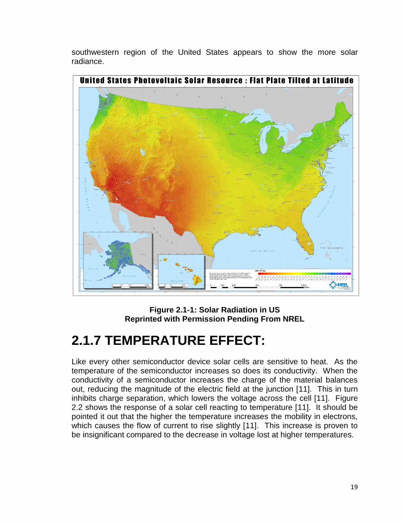
19
southwestern region of the United States appears to show the more solar radiance.
Figure 2.1-1: Solar Radiation in US Reprinted with Permission Pending From NREL
2.1.7 TEMPERATURE EFFECT: Like every other semiconductor device solar cells are sensitive to heat. As the temperature of the semiconductor increases so does its conductivity. When the conductivity of a semiconductor increases the charge of the material balances out, reducing the magnitude of the electric field at the junction [11]. This in turn inhibits charge separation, which lowers the voltage across the cell [11]. Figure 2.2 shows the response of a solar cell reacting to temperature [11]. It should be pointed it out that the higher the temperature increases the mobility in electrons, which causes the flow of current to rise slightly [11]. This increase is proven to be insignificant compared to the decrease in voltage lost at higher temperatures.
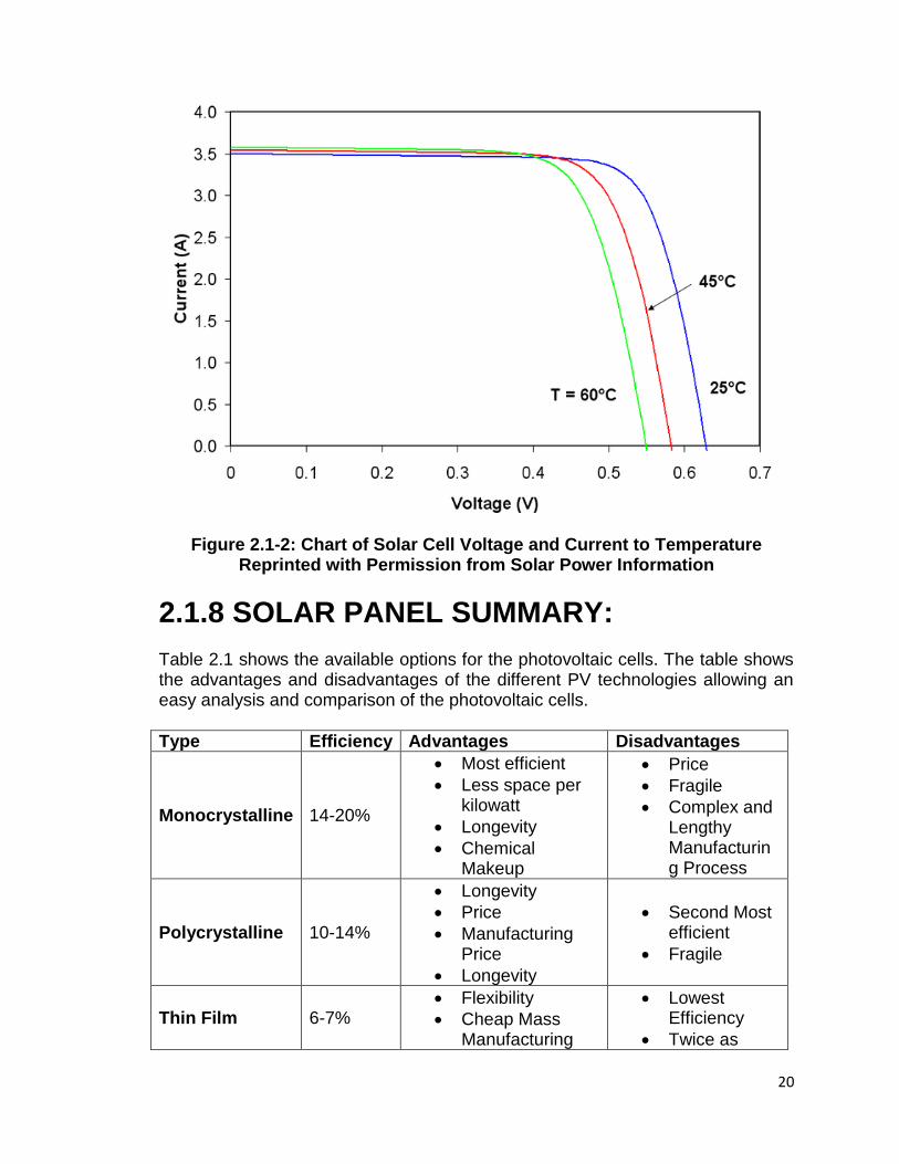
20
Figure 2.1-2: Chart of Solar Cell Voltage and Current to Temperature Reprinted with Permission from Solar Power Information
2.1.8 SOLAR PANEL SUMMARY: Table 2.1 shows the available options for the photovoltaic cells. The table shows the advantages and disadvantages of the different PV technologies allowing an easy analysis and comparison of the photovoltaic cells.
Type Efficiency Advantages Disadvantages
Monocrystalline 14-20%
Most efficient
Less space per kilowatt
Longevity
Chemical Makeup
Price
Fragile
Complex and Lengthy Manufacturing Process
Polycrystalline 10-14%
Longevity
Price
Manufacturing Price
Longevity
Second Most efficient
Fragile
Thin Film 6-7% Flexibility
Cheap Mass Manufacturing
Lowest Efficiency
Twice as

21
Durability
More Efficient in Heat
10% Less Weight
Most Efficient in Low Light
much space needed per kilowatt
Mounting Cost
Unknown Longevity
Table 2.1-1: Overview of Different Solar Panel Technologies
2.2 INVERTERS: An inverter is a device that is responsible for converting DC to AC. An inverter should not be confused with a converter (regulates DC voltage) or a transformer (regulates AC voltage). An inverter is like a backbone for most solar power systems. The inverters most basic function is to invert DC electricity coming from solar panels into AC electricity with or without a battery connected in the middle of solar panels and inverter. Although there are some appliances and machines that can run directly with DC, most appliances are run only with AC and that is what feeds into regular wall power outlets in households, which makes it necessary to use an inverter with solar panels since solar panels are only capable of producing DC. Here we look at two kinds of inverter before we go into details about features and specifications of the inverters.
2.2.1 OFF-GRID INVERTERS: In simple words, off-grid inverters their energy in batteries and stored energy could be used instantaneously to power appliances. Just like any other power inverters, Off-grid inverters also convert DC to AC for household usage. As obvious by its name, Off-grid system is absolutely independent of the utility grid, also known as stand-alone inverters, which means you will not have to play with the grid to hook them up. The independent nature of these inverters makes them an ideal candidate for rural areas or mobile applications such as on boats where grid power is not available. These inverters can also be used to supplement a power generator in case of the generator not meeting the power usage requirement. Anti-islanding protection is not necessary for these inverters as they are stand alone system. The reason they cannot be tied into the grid is because they are not capable of synchronizing the output phase with the phase of the power grid. Since these inverters are not connected to the grid, we can‟t really sell the energy back to power company even if the system is producing more energy than needed. The excess energy production will just go to waste.

22
Here at UCF, we are aiming to use all the energy produced by the PV farm since our power consumption is so high and also we would need to provide the power to several different areas on campus which will require the grid connection and matching of phases. Therefore Off-grid inverters are out of the question for us. We will have to choose something more compatible.
2.2.2 GRID-TIE INVERTERS: A Grid-tie inverter is an inverter that allows solar energy produced by the PV panels to be connected to the power grid directly without batteries. First it regulates the voltage and current from DC coming in from PV panels and then it converts DC into AC. Grid-tie systems do not charge batteries which means they cannot provide any back-up power in case of power outage. This means, these inverters will only be useful in the daytime when sunlight is available. Hence, we can‟t take advantage of these inverters at night time since they will be dead at night. Grid-tie inverters do require anti-islanding protection which means they will not be functional in case the grid power is turned off. The main advantage of Grid-tie is they make sure that the solar energy converted from DC to AC is in phase with the grid power. Now, if we produce excess energy, the meter would reverse and the extra energy production will be fed directly to the power company, which means we can actually get paid for supplying the energy to the power company. With this battery-less system, the hassle of buying batteries and replacing the periodically can be eliminated. Also we will not have to monitor the batteries for their functionality. Excess energy will simply be handled by the grid, hence, providing a self-regulating system that needs very little attention in long run. There is a kind of inverters which is hybrid of both Off-grid and Tie-grid inverters and is called Grid-tie with back-up. It performs all the desired functions, stores the energy into batteries for back-up, synchronizes the phase with the grid power, and sells the excess power back to the power company. These inverters sound fancy and obviously the come with a very expensive price tag. Again, our goal is neither to store energy nor sell the energy. We will be using all the energy produced from our PV farm and since our power consumption peak hours matches with the power production peak hours, there is no need to store the energy. In order to sell the energy we will have to build a PV farm much bigger than what is suggested now. So, this discussion leads us to pick the Grid-tie inverters because they fit just right for our project requirements. Table 2.3.1 represents the key features of the three different inverters discussed.

23
INVERTER TYPE BACK-UP POWER SELL BACK
Off-Grid YES NO
Grid-Tie NO YES
Grid-tie with back-up YES YES
Table 2.2-1: Comparing Inverters with Back-up power and Sell Back
2.2.3 INVERTER FEATURES: When picking an inverter for the project, it is very important to look at features and specifications of an inverter which suit your project the best. The most important thing is the inverter‟s AC output waveform. The ideal AC waveform is a pure smooth sine wave. However, not all inverters are capable of producing pure AC sine wave. Now we look into a couple of different waveforms that can be produced by inverters.
2.2.4 MODIFIED SINE WAVE INVERTERS: Modified Sine Wave is the wave produced by generic or cheap inverters and can be used to power appliances which do not need accurate timing like an oscillating fan. The sine wave produced by these inverters looks more like a square than a curve. Because of its nature we can also call it a modified square wave. Since this wave form is not smooth and has sharp edges, it causes problem with certain appliances. Appliances or equipments powered by modified sine wave tends to causes noise and draw more power and get heat up. Digital clocks and timings of appliances can be jeopardized and sensitive electronic items can be damaged by modified sine waves. Modified sine wave inverters cannot be tied into power grids due to their inefficiency. A modified sine wave can be seen in figure 2.3.2. An upgraded version of modified sine inverter is available now and is known as stepped-sine wave. Stepped-sine wave inverter is much more efficient than regular modified sine wave inverters. The wave form produced does have curves but contains small little sharp edges as in stair steps. These inverters can be tied into power grids but are equally as harmful as a modified sine wave inverters to sensitive electronic equipment. A stepped sine wave is shown in figure 2.3.2.
2.2.5 PURE SINE WAVE INVERTERS: The output wave form a pure sine inverter is clearly a pure sine wave with very low harmonic distortion and clean power, just like the one supplied by power

24
companies. These can be hooked to the power grids without any issues and electricity could be sold back to power companies. Electric appliances ruuning on pure sine wave performs faster, quieter and cooler. Pure sine wave also reduces the noise in appliances significantly. A pure sine wave form is shown in figure 2.3.2. Having so many advantages over modified sine wave inverter, pure sine wave inverter does come with a heavy pricetag, almost twice the price of a modified sine wave inverter. In conclusion, we decided to choose a pure sine wave inverter to avoid the hassle of appliances and equipments not working properly because of discrepancy in the shape of sine wave form.
Fig. 2.2-1 Curve: Pure wave; Long edges: Modified wave; Short edges: Stepped wave
2.2.6 INVERTER PRICE, QUALITY AND SIZE: An aspect of the inverter we should not be scared of when buying an inverter is the price of it. Always buy a higher quality even if we have to pay a little bit more money and always pick a well known company. Choosing an inverter in this manner pays off in the long run and saves us money and stress. It is equally as important to pick the inverter depending on the size of the load. For example, if we were to run just a washing machine that requires 110 V and consumes 500 W, we are better off buying a modified sine wave inverter with maximum output power of 700 W. There is no need to buy one that can power up to 2000 W. Buying higher power than needed, will be just the waste of money. On the other hand, not buying enough power inverter is also a waste of money and power generated through solar panels or any other source. In above example, buying an inverter that can only power up to 400 W is an example of such scenario. After all the discussion and research about the inverters, and keeping all the factors in mind, we decided to go with Fronius IG 3000. The chosen model is

25
made exclusively for PV panels and equipped with all the necessary modules. The Fronius lG 3000 is discussed below.
2.2.7 CHOSEN INVERTER: Fronius LLC has been engaged in production and development of solar electronics since 1992, photovoltaic inverters in particular for grid-tie and off-grid. They have a large number of renowned manufacturers and wholesalers of solar modules as their satisfied customers. Fronius has advanced to the ranks of the worldwide leading manufacturers and continues to develop its position through ongoing product innovations. The Fronius IG series has proven itself to be powerful, user-friendly and highly reliable. These are suitable for every size of PV system, especially for smaller systems. The ingenious processor control combined with the powerful HF transformer extracts the maximum energy yield from all types of modules.
2.2.8 FRONIUS IG 3000:
Fronius lG 3000 is equipped with an LCD display which can display output voltage and output current. It has its own memory module which keeps the data stored for a certain period of time. Let‟s say if we wanted to copy the readings for past five days, it will be possible with such inverter. We can easily stick a flash drive and copy the data required. It is water-proof, weather-proof and long lasting, which means we can just hook it up to the panels and set it on a side without worrying about making a protective casing for it. Although we will put it in a protected casing just for the safe side, but it is not required. It has a self cooling mechanism which keeps it cool. Unlike some other inverters which can only input 12 V DC which require parallel connection of solar panels, Fronius IG 3000 can input high voltage so we can set up the solar panels in series connection. It comes with anti-islanding protection and certified with UL 1741 and IEEE 1547. Table 2.3.2 mentions the key specs and features of this wonderful piece of technology.
Figure 2.2-2: Fronius IG 3000

26
Reprinted With Permission Pending from Fronius.com
Input Data (DC)
Power 2500-3000 W
Max. input DC voltage 500 V
Operating voltage range 150 - 450 V
Max. input DC current 13.6 A
Output Data (AC)
Max. output power 2700 W
Nominal output voltage 240 V
Utility voltage range 212 -264 V
Max. AC current 11.25 A
Feedback current 0.0 A
Operating frequency 60 Hz
THD less than 5%
Power Factor 1
General Data
Max. efficiency 95.20%
Weight 26 lbs
Temperature Range −5 F to 122 F
Table 2.2-2: Specifications for Fronius IG 3000
2.3 COMBINER BOX: In a nutshell, a combiner box is where all the solar panels arrays will be combined. We are still debating on using a combiner box. Since we are planning to make only one array of panels, it is really not necessary to use one. However, if we do use a combiner box, in future, it will allow us to connect multiple arrays of solar panels to one combiner box. The Combiner Box is an electrical distribution box where the DC circuit breakers are placed. The Combiner Box combines the multiple DC inputs coming from the Array terminations and converts these into one DC output. The output of the combiner box is connected

27
to the charge controller or the inverter, depending on the type of system installed. We will be using an inverter, so it is feasible to use the combiner box. In order to choose the correct combiner box, it is necessary to determine the number of strings of the solar panels, since a breaker is needed for each string. It is also required to determine the breaker's size that is needed based on the string‟s current and voltage. For example, a system with four 100 volt, 10 amp strings requires four 125 volt, 20 amp breakers. Even though each string only generates 10 amps of current, a 20 amp breaker would suffice, as a 10 amp breaker may flip too often. [12] The string of solar panels simulated in our project consists of 12 solar panels connected in series, with each producing 32 Volts and 7.5 Amp the combined voltage of that string would be 384 volts at 7.5 Amp. So with the recommendations above it‟s necessary to use a breaker with values that exceeds these specifications. On SUNELECT website we found a fuse able to handle up to 600VDC and 20 Amp which are the values able to handle our system without much interruption on fluctuations. (MNFUSE20) the fuse selected is shown in figure 2.3.3.1
Figure 2.3-1 MNFUSE20 Reprinted with Permission Pending From Sun Electronics
A Touch Safe Holder is required to position the fuse in the combiner box and it should be able to handle the voltage and current coming from the solar array it connects to. The part selected is MNTS which is designed for 10x38 mm fuses 600VDC 30 Amp Din rail mount in the MNPV combiners for high voltage string inverters. A picture is shown figure 2.3.3.2. the figure shows some of the specifications of the device, its an easy to install holde, to be inserted in the openings of the combiner box. In this project only one breaker will be rquired because of the serial connection of the twelve panels.

28
Figure 2.3-2 MNTS Reprinting with Permission Pending from Sun Electronics
The combiner box is it to be placed outside in the open so it is necessary to choose one with high weather tolerance able to handle the heavy rain, high wind speeds, and high ambient temperatures. The best price for such a combiner box was found on SUNELEC website for 81.00$ a picture of this box is shown in figure 2.3.3.2. it is possible and easy to build our own combiner box using a typical home AC breaker panel which takes in 1 AC input and distributes to several AC circuits so it is essentially reversing its functionality and using it as a combiner instead of a splitter our main motive for designing this part is an attempt to reduce the cost of our design but after considering the prices of circuit breaker panels they ranged from 30$ – 40$ which is not a great saving compared to the 80$ combiner box found online which is built to with stand the rain and the rough outdoor conditions.
Figure 2.3-3 Combiner Box MNVP3 Reprinted with Permission Pending from Sun Electric

29
2.4 SURGE ARRESTOR:
When installing outdoor electric power systems, we have to keep in mind to protect the system from natural disasters. We are taking multiple steps to keep the system protected from rain up to 100% but the rain is not the only candidate, lightning strikes are very possible in open field while it is raining. We have to protect the system from the sudden high voltage spike in case the system is hit by lightning. We need to protect the electricity distribution and supply both from lightning. The most effective means of protection is the use of surge arresters by installing it properly close to the electric system. Surge arrestors act like clamps in most cases. They will connect to the live wires and to the wire going to the ground. In normal conditions, they do not perform any function but in case of a voltage spike, the surge arrester starts conducting and it will short the dangerous high voltage to ground. For the system to have best protection, a DC surge arrestor will be needed at the solar panel end and an AC surge arrestor after the inverter. A surge arrestor can divert the surges indefinitely as long as the energy dissipated is in the range of the arrestor. In case of lightning, the surge is obviously much higher in range; it shorts the circuit by destroying itself. And we can easily replace the destroyed surge arrestor with a new one. Surge arrestor used to come in porcelain housing but now they are coming in silicone housing because silicone is known to perform a better short-circuit and provides better protection to the other components of the system. The surge arrestors are not perfect, but it is a much better idea than using nothing at all because without a surge arrestor, the whole system could be destroyed in a matter of seconds causing thousands of dollars of damage. So it is better to invest in buying a surge arrestor to save the investment of much higher amount. Figure 3 shows a typical setting of a surge arrestor in the system.
Figure 2.4-1- Surge Arrestor Location

30
2.5 WIRES AND CONNECTORS: The solar panels we have picked are already equipped with wires but we will still need some sort of wires to go between the last solar panel in the array and another wire to go between the combiner box and the inverter. Normally the “complete grid tie PV systems” provided by the manufacturers use MC4 connectors for their connectivity. So we have decided to go with MC4 connectors for our system as well. We chose Samlex's MC4-2 connectors which is the latest in MC4 series. We will need two 30ft PV wires according to our connection and each wire will have one male and one female MC4 solar panel connector. MC4 connectors are shown in figure 1. MC4 connector system is really easy to install, for example, the male end snaps right into the female end. This snap-in quality makes it very reliable against any unintentional disconnection. When the two contacts are locked in, the connection is sealed against entering of water or dust into the connection. Following are the specs of MC4-2 connector:
Wire size AWG # 10 or AWG # 12 with outer insulation diameter of 3 – 6 mm
Contact diameter of 4 mm
Maximum current capability - 30 A
Maximum voltage capability - 1000 V
IP67 protection (dust tight, liquid immersion up to 1 m)
Temperature range 40°C to +90°C
UL listed
Figure 2.5-1: MC4 connector, male and female
As explained earlier, the solar panels we chose will come with approximately 3 ft of positive („+‟) and 3 ft of negative („-„) wire. One end of each wire will be connected to the junction box of the panel. The chosen solar panel‟s wire is terminated with an MC4 connector. The Positive („+‟) wire has a Female MC4 Connector and the Negative („-„) wire has a Male MC4 Connector. A typical setup for MC4 connector connectivity to the wires coming out of the solar panel is
31
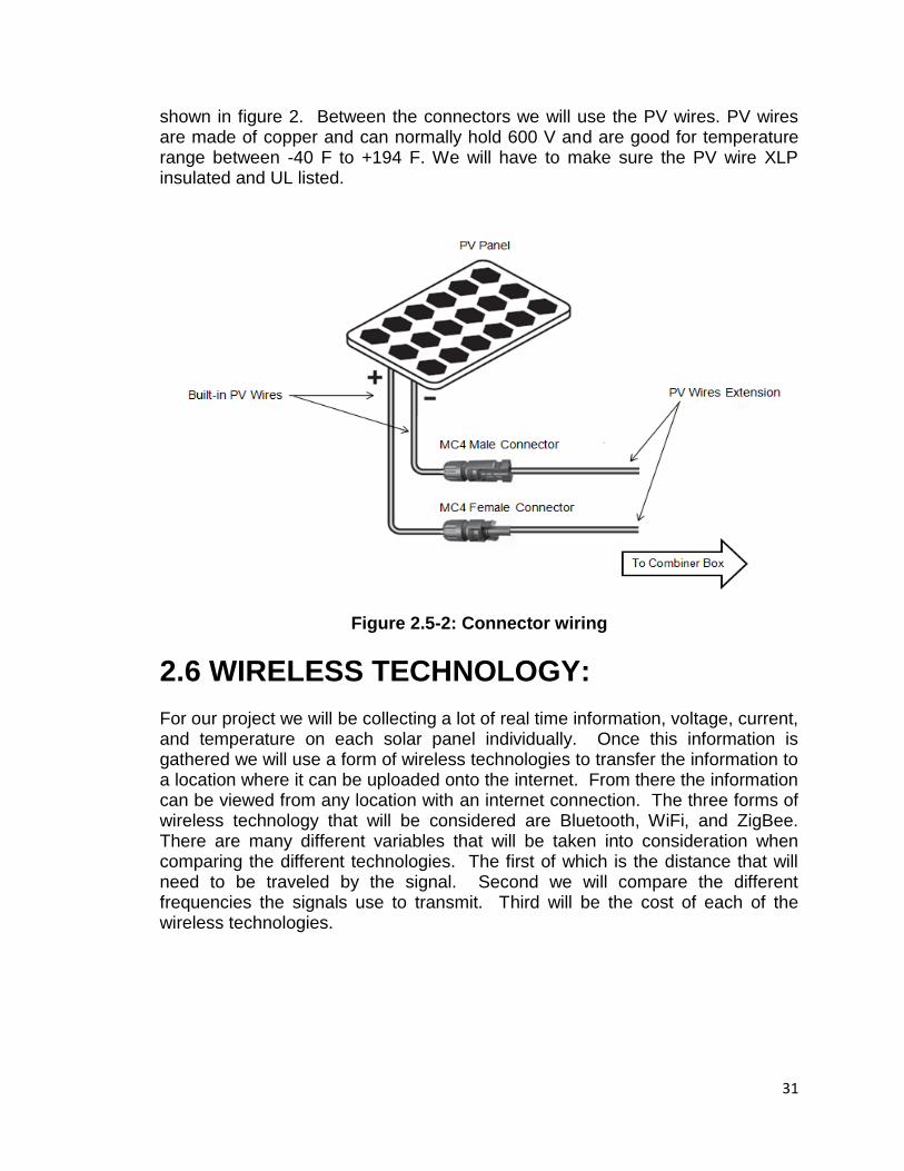
shown in figure 2. Between the connectors we will use the PV wires. PV wires are made of copper and can normally hold 600 V and are good for temperature range between -40 F to +194 F. We will have to make sure the PV wire XLP insulated and UL listed.
Figure 2.5-2: Connector wiring
2.6 WIRELESS TECHNOLOGY: For our project we will be collecting a lot of real time information, voltage, current, and temperature on each solar panel individually. Once this information is gathered we will use a form of wireless technologies to transfer the information to a location where it can be uploaded onto the internet. From there the information can be viewed from any location with an internet connection. The three forms of wireless technology that will be considered are Bluetooth, WiFi, and ZigBee. There are many different variables that will be taken into consideration when comparing the different technologies. The first of which is the distance that will need to be traveled by the signal. Second we will compare the different frequencies the signals use to transmit. Third will be the cost of each of the wireless technologies.

32
2.6.1 WIFI TECHNOLOGY: WiFi is a wireless technology that was developed in the late 1990‟s. It is also known by the technical term “IEEE 802.11”. WiFi is the most popular wireless technology on the market with hundreds of thousands hotspots and millions of people using it worldwide. Being the most use wireless technology in the world there are many different standards of WiFi technology on the market. With each standard of WiFi technology possessing different strengths and weaknesses we will look at all four types of WiFi technology. There are four different standards of WiFi: 802.11a, 802.11b, 802.11g, and 802.11n.
2.6.1a: 802.11a: This standard of WiFi technology is referred to as “Wireless A” and was the developed in 1999. It can transfer data at a rate of 54 (Mbps) using the 5 (GHz) radio band. Although when first developed the 802.11a technology was high priced, unreliable, and medium ranged it has since been updated. Today the 802.11a has range virtually equal to that of 802.11b and the reliability has been improved. The price of parts has also decreased considerably since the time it was first developed. The typical indoor range is about 100 ft, while the typical outdoor range is 300 ft [13].
2.6.1b: 802.11b: Developed later in 1999, 802.11b known as “Wireless B” gained a majority of its popularity in late 2000. 802.11b uses the radio band at 2.4 GHz. This lowers the maximum data rate to 11Mbps, though the typical throughput fluctuates between 6 and 7 Mbps [13]. Although the 802.11b is reliable at a low cost it does have a couple disadvantages. First it shares the 2.4 GHz radio band with many other devices such as, cordless phones, microwave ovens, and Bluetooth modules. Because of this 802.11b can suffer from interference issues. Nevertheless because of its reliability 802.11b is still typically used in many point to point and point to multipoint long distances applications [13]. The typical indoor range is about 100 ft, while the typical outdoor range is 400 ft [13].
2.6.1c: 802.11g: Developed in 2003, 802.11g known as “Wireless G‟ is considered the high speed replacement of 802.11b. 802.11g uses many of the same modulation techniques as 802.11a but shares the 2.4 GHz radio band as 802.11b. Because it shares many of the same modulation techniques 802.11g has a data rate at 54 Mbps but is typically clocked with a throughput of 19 Mbps. One of the advantages of 802.11g other than its high throughput is that it can be used simultaneously with 802.11b to give the client more reliability and backwards compatibility as a

33
cheaper cost. The typical range for 802.11g is the same as 802.11b and also shares similar interference issues from other devices on the 2.4 GHz radio band.
2.6.1d: 802.11n:
Developed in 2009, 802.11n known as “Wireless N” is the newest and fastest WiFi technology. This new technology has many advantages mixing a lot of the earlier WiFi technologies characteristics. 802.11n can use both the 2.4 GHz and the 5 GHz radio bands. With a maximum data transfer of 600 Mbps on the 5 GHz radio band it is almost 6 times faster than earlier WiFi technology. Typical throughput however is 75 Mbps depending on signal quality [13]. Another benefit of an 802.11n router is that is can simultaneously communicate with 802.11b, 802.11g, and 802.11n devices. This gives the client a wide range of compatibility with older technology. Although this new WiFi technology offers many benefits it does come with some disadvantages. Firstly because it uses multiple channels to send and receive data, it requires multiple radios, this raises the cost for the client [13]. Also the speed of routers is limited to the number of antennas the client‟s WiFi device is equipped with. The typical indoor range is 200 ft, while the typical outdoor range is 800 ft [13]. Below is a list of WiFi advantages and disadvantages along with a table comparing the four different kinds of WiFi. Advantages:
Can be installed some places where wires cannot go.
WiFi is very low in cost
Many different options to custom build your own wireless system with.
Installation is often fast and easy
Does not get affected by wire wear and tear.
Disadvantages:
The 2.4 GHz radio band is very crowded with many other devices using it, this can cause interference
The more devices connected to a WiFi router the lower the data rate for each device is
Security is more difficult to guarantee
Slower speed then wire communication
WiFi Technology
Data Rate Frequency Typical Indoor
Range Typical Outdoor
Range
802.11 (Mbps)
(GHz) (ft) (m) (ft) (m) Max Typical
a 54 24 5 100 30.5 300 91.5
b 11 6-7 2.4 100 30.5 400 122

34
g 54 19 2.4 100 30.5 400 122
n 600 75 2.4/5 200 61 800 244
Table 2.6-1 : Specifications of different WiFi Technologies
For our project a distance greater than 800 feet will be needed to transfer the data from our monitoring system to a computer with wired internet connection. For this reason WiFi is not the best option for us.
2.6.2 INFRARED: Infrared wireless communication is commonly known as IR wireless. It is the form of wireless technology that uses infrared radiation to communicate data. It is the oldest way of wireless communication between two devices. It has a wavelength somewhat longer than the wavelength of red light. Infrared is not visible to a naked eye. On an electromagnetic radiation spectrum, it falls between visible red light and radio waves with the shortest wavelength bordering with visible red, and the longest wavelength bordering with micro waves. IR wavelength could vary from 0.7 - 100 micrometer, and frequency could be in the range of 3 to 430 THz. IR technology also allows computers to communicate through short-range signals. Computers can transfer files and other digital data bidirectional. Infrared is relatively a cheap way to provide communication between two computers or devices. The most commonly used infrared connectivity is known as point-to-point system. In point-to-point system, the receiver and the transmitter must be facing each other and there should not be any obstacle between them, the line of sight must be clear. This link is created between the transmitter and the receiver to transfer data back and forth through IR. The transmitter converts an electrical signal to an optical signal through an LED or LD (Laser diode) and the receiver in turn convert the optical data into the electrical data. IR data communication speed is up to 4 Mbps. Some IR wireless communication advantages and disadvantages are discussed below. Advantages:
IR requires very low power to operate.
Extremely cheap to build a circuit board for IR.
Data transfer is highly secure because of its direction; data cannot be leaked or hacked.
It is immune to high noises, which means it normally doesn‟t have interference from other devices.
IR is much more reliable than wired connections as it doesn‟t require any pins or plugs and no wear and tear of wires.
Disadvantages:
Transmitter and receiver should be aligned to each other.

35
IR wireless cannot pass through walls and most solid objects.
Bidirectional IR has a very short range (0-1m)
Communication speed slows down with increment in distance.
Slower speed than wired communication.
Do not perform well outdoors because of Sun‟s infrared radiation interference.
From the discussion of IR wireless, it looks like IR is not a good candidate for our project. We definitely need something faster, long-range and also which is not affected by solar radiation.
2.6.3 BLUETOOTH TECHNOLOGY: Bluetooth is an proprietary open wireless technology standard for exchanging data over short distances (using short wavelength radio transmissions) from fixed and mobile devices, creating personal area networks (PANs) with high levels of security [14]. Bluetooth technology was designed to be easy and simple for new users, allowing them to easily connect low bandwidth wireless devices. In the wireless and handheld market Bluetooth is closely related to infrared technology. One of the major differences between Bluetooth and infrared technology is the need of infrared to have line of site between the devices using it. This is a major advantage for Bluetooth as it is not a line of sight technology. Depending on the version of Bluetooth you can also receiver different data rates. Starting with the slowest version, version 1.2 offers a data rate of 1Mbps. The next fastest is version 2.0+EDR with a data rate of 3Mbps. The last but fastest Bluetooth technology is version 3.0+HS offering a data rate of 24Mbps. Bluetooth also has been proven to provide ranges of up to 100 m, 10 m, and 1 m depending on the class of Bluetooth you are using. For the longest range the Class 1 Bluetooth is needed as it is the class that offers the 100 m range. Class two offers approximately 10 m and Class three offers the shortest range with approximately 1 m. Another benefit with blue tooth technology is that it like ZigBee requires low power. It also is low processing with and overhead protocol. Both of these abilities make Bluetooth technology great for integration with small battery powered devices, making the applications of Bluetooth nearly endless. Although Bluetooth technology offers many benefits to a wireless system there are a couple of limitations that should be taken into consideration when designing your wireless system. The first of which is the lower data rate. Also the 100 meter range is ideal for short range wireless systems but with ZigBee-Pro offering ranges upwards of 1300 meters Bluetooth might not be the wireless technology for your system. Below is a list of Bluetooth advantages and disadvantages along with a table comparing the three different Bluetooth classes and versions. Advantages:
Bluetooth technology is inexpensive

36
Bluetooth is automatic and does not require any configuration to connect with any other Bluetooth device within range.
Avoid most if not all interference.
Low energy consumption
Upgradable Disadvantages:
Low data rate
Relatively small range
Bluetooth Technology
Max Power Permitted
Range
Class mW dBm m
Class 1 100 20 Up to 100
Class 2 2.5 4 Up to 10
Class 3 1 0 0.1-1
Version Data Rate
Mbps
1.2 1
2.0 + EDR 3
3.0 + HS 24
Table 2.6-2 : Comparisons of Bluetooth Classes and Versions
Although Bluetooth technology has considerably more advantages then disadvantages for our project it does not possess the data rate or range we are looking for. For those reasons Bluetooth is not best option for us.
37
2.6.4 ZIGBEE TECHNOLOGY: ZigBee is a specification for a suite of high level communication protocols using small, low-power digital radios based on the IEEE 802.15.4-2003 standard for Low-Rate Wireless Personal Area Networks [15]. ZigBee was designed to address the unique demands of sensor and control of network applications and remote monitoring. One of the main advantages to using ZigBee is its ability to operate at low powers. This allows ZigBee to have a longer battery life in general and can be used with smaller batteries then other wireless technologies. The technology surrounding ZigBee was designed to be simple and less expensive than other wireless technologies, such as Bluetooth or WiFi. ZigBee sensor networks require far less high throughput but offer even greater flexibility than other network types [16]. Thus, these networks are well suited to applications requiring low data rate transmissions [16]. As a result of ZigBee lower throughput the cost is less, battery life is longer, and the complexity of the system is much less. Another unique feature about ZigBee technology is with sensor networks RF frequencies are allocated. This is an added benefit because the wireless signals from your system will be separated from WiFi and other traffic. This prevents the ZigBee‟s transmission from the battle of bandwidth that may affect critical applications when converging RFID-RTLS with WiFi. To accomplish this ZigBee technology uses the IEEE 802.15.4 physical radio specification and operates in unlicensed bands worldwide at the following frequencies: 2.400-2.484 GHz, 902-928 MHz and 868.0-868.6 MHz [17]. The two types of ZigBee technology on the market right now is the XBee and the XBee-Pro. The XBee has an outdoor distance of 470 – 845 ft depending on the antenna used, while the XBee-Pro increases this range to 1 mi. Another important difference in the specifications between the XBee and the Xbee-Pro is the power consumption. The Xbee uses 55mA while the Pro uses 215mA. Below is a list of ZigBee advantages and disadvantages along with a table comparing the four different kinds of wireless technology. Advantages:
Low power consumption – longer battery life
With ZigBee-Pro range reaches up to a mile
Low Latency
128-bit AES encryption for secure data connections
Supports mesh networks
Disadvantages
Low data rate
Price is higher than other wireless technologies

38
Wireless Technology
Radio Band Frequency
Data Transfer Rate
Range Cost
(GHz) (Mbps) (ft) (m)
WiFi
802.11a 5 54 300 91.5 Low
802.11b 2.4 11 400 122 Low
802.11g 2.4 54 400 122 Low
802.11n 2.4/5 600 800 244 Medium
Bluetooth
Class 1 2.402-2.480 1 Up to 329 Up to 100
Low
Class 2 2.402-2.480 3 Up to 33 Up to 10 Low
Class 3 2.402-2.480 24 0.1- 3.28 0.1-1 Low
ZigBee
Standard 2.4 250 kbps 300 90 Medium
Pro 2.4 250 kbps 5280 1.6k High
Table 2.6-3 : Direct Comparisons of Wireless Technologies
For our project it was determined by the group to design our system with a ZigBee XBee-Pro. We decided to go with an XBee-PRO because of its range. This is the only wireless technology that is able to send a signal far enough for our project.
2.7 WIRE TRANSMITTION TECHNOLOGY: 2.7.1 DIRECT WIRE COMMUNICATION: Wired technology has been around since the early 1900‟s with the introduction of the telephone network. The use of wired connections created many other technologies, included multiplexing and SONET. Wired technology is a very

39
reliable technology which works by transmitting electric signals of a metal conductor. The reliability of wire technology comes for the protection of the wires insulation that is wrapped around the metal conductor. Presently this is the most reliable method of transmitting/receiving data or sound throughout the world. Currently with the use of TI, T3, and fiber optic cables the internet sends millions of gigabits of information through the world. Advantages:
Near 100% Reliability
Easier to trouble shoot wired systems
Low priced
Not affected by weather
High speed
Information is secure Disadvantages:
Length of Wire limits distance
Can b affected by moisture
May cause maintenance problems with wire corrosion over time
2.7.2 POWER LINE COMMUNICATION: Power Line Communications is any technology that enables data transfer at narrow or broad band speeds through power lines by using advanced modulation technology [18]. Power line communications is capable of transmitting data via electrical lines, and therefore can extend an existing local area network or an existing internet connection through electric plugs with the installation of specific units [18]. The main signal in a PLC is superimposed at a high frequency (1.6 to 30 MHz) at low energy levels over the 50 Hz electrical signal. A second signal is transmitted through a power infrastructure and can be received and decoded remotely [18]. Also and power line communication receiver can receive the message as long as it is located on the same electrical network. One downfall to power line communications is the legal framework and regulation. At the moment since PLC networks are both electrical supply networks and telecommunication networks there is no precise regulation that exists for a PLC network or equipment. Because of this the installation of power line communication networks behind a private meter is unregulated, though if the network causes negative side affects the system must be taken down. When a power line communication network is installed outside a private meter with the signal transmitted at the HVA/LV transformer level creating electrical loops, testing permits are required. To obtain these permits the client must go through Telecommunications Regulatory Authority so long as the technology is still being developed with no specification standards published.

40
Advantages:
Can use an existing infrastructure
Unaffected by wireless „noise‟ making the system very reliable
Wired communication have higher data rates than that of wireless technology
Since the wire is enclosed the security of the signal is very good Disadvantages:
No legal regulations on specification standards set in place as of now
Wires can get tangled and messy within the system
Length of wire is the limitation to distance
Impedance of the wire can affect your signal.
2.8 WIRELESS VS WIRED TECHNOLOGY:
2.8.1 WIRES: Wires in general have many advantages over wireless technologies. First it is a very secured and fast way of transferring data. Wire technology is the fastest way of sending data in the world right now. Also the reliability for wired technology cannot be matched. The term “reliability of the five nines” was coined from the telephone lines 99.999% uptime which is accomplished by the wired system is it implemented with. Also like wireless the signal can be exposed to noise within the wired lines. This is mostly due to either a magnet or loud machinery noise. Unlike wireless the cost and solution for blocking noise in a wire is cheap and easy. Generally shielded or armored wiring is used to protect against weather and other type of negative externalities. Also copper wiring has a very long life expectancy. The QoS is excellent because wired connections eliminate the need for establishing an end-to-end connection every time. Another great advantage to have wired technologies is that certain wires can contain multiple conductors within them. This all you to control the data being sent through the wire better. Although wires offer many great qualities they are not always a realistic way of designing a system. For one in rural areas that are not prewired for internet or TV, consumers are forced to use satellites signals in order to obtain the information. Also there are limitations on the length a wire can be before the signal might need to be boosted due to the impedance of the wire. The longer the wire is the more the impedance the wire has, this dampens the signal enough that the desired output is not obtained. For example Ethernet cable can run a max of 100 meters before the signal needs to be enhanced. For this reason specialized wires have been developed with low impedance which helps preserve the strength of the signal. To obtain these specialized wires are quite a bit more money though, adding another disadvantage for wired technology.

41
2.8.2 WIRELESS: Wireless technology has many benefits that wires cannot give you. The first one and probably the most important is the convenience. The ability to replace dozens of wires stretching hundreds of feet throughout your house with a single wireless router is its biggest advantage. You also don‟t have to worry about running wires into tight places, or obtaining low voltage permits. Another added benefit to wireless technology is that the impedance of air is very little, this allows you to take full advantage of the impressive ranges the technology offers, without having to boost the signal. Also the transmitter and receivers may break, the signal will never with always be preserved in the air. On the other hand wires although having long life expectancies will become old and can corroded. Like any other technology wireless does have its disadvantages. The first of which is interference. With many wireless devices operating on the same radio bands there is a lot of traffic that can slow down your signal. Another source of interference is EM (electro-magnetic radiation), wires can also be affected by this but wireless devices are helpless whereas wires can be shielded from the radiation with insulation. Another downside to wireless is the price of equipment, as well as the installation of the equipment which can be tricky at times. Debugging a wireless system can also be a headache, with a wired system you can follow the wires and trace the signal. With wireless signals there is no way to trace the signal in the air, this gets exponential harder with multiple wireless signals are being transmitted at once. Security is also a major problem with wireless signals. This can be reduced with encryption and passwords but without the ability to limit the signal other than the transmitters range. The possibility of being hacked it always present. Wireless signals also lack the speed of their wire counter parts. Although with the new data rates of 102.11n reaching up to 600 Mbps, it is not even close when compared to the gigabyte or 10 gigabyte speeds that are attainted using wires. Lastly the reliability of wireless signals although improved will probably never reach that of wires. There is just too many variables to consider not allowing you to reach the “reliability of the 5 nines”.
Wireless Wired
Price Medium Low
Life Expectancy Can be Affected by
Heavy Rain and Snow
Shielded from Weather by Insulation
Speed Medium High

42
Noise Affected by other wireless signals
Not affected by other signals but
can be affected by magnetic fields
Security Signals can be easily
intercepted High level of
security
Reliability Medium Very high
Distance Unlimited Limited by Length
of Wire
Table 2.8-1: Comparing Wireless and Wire Technology
2.9 ANALOG VS DIGITAL: The first design problem our team faced was to figure out what kind of signal we wanted to send from the PCB board at the panel to the main PCB board. The two options of signal we had were digital or analog. Either type of signal came with its strengths and weaknesses and would require the design of the PCB boards to be drastically changed.
2.9.1 ANALOG SIGNAL: An analog signal is a continuous signal that follows transmissions standard that emulates the audio waveform of sound using electrical impulses. This type of signal gives you some great advantages to that of a digital signal. The first and man advantage of a analog signal is that an analog signal has the potential for an infinite amount of signal resolution. Being of a higher density then digital signals analog signals are more accurate. When dealing with sensors that need a certain level of accuracy this advantage was very intriguing to our team. Another large advantage to analog signal is that they use less bandwidth then that of digital signals. This is extremely important as it allows us many different options on how to send the signal from one board to another. An analog signal can also be processed easier and simpler then that of their digital equivalent. Analog also offer a last advantage when designing our project. The ability to multiplex analog signals simplifies our design by allowing us flexibility with the microcontroller we choose. By keeping our design options open our design was only limited on current technology, money, and our own minds. Although having some very good benefits analog signals do have their downfalls. The biggest of which is the effect noise has on the signal. Random noise can

43
affect an analog signal enough that the signal experiences loss and distortion impossible to recover. The signal is impossible to recover due to the fact that even amplifying the signal to recover attenuated parts also raises the noise. Because of the noise even if the resolution of an analog signal is higher than that of a digital signal the difference can be negated. Also if setting up an analog signal system an upgrade to a digital interface is not possible, meaning if a certain process isn‟t available except for in digital form the whole system must be redesigned. Furthermore analog signals sometimes require the clock and phase of TFTs to be synchronized to avoid pixel jitter. The technique to synchronize the clock and phase is a very complex and complicated issue.
2.9.2 DIGITAL SIGNAL: A digital signal uses distinct electrical or optical pulses represented using binary digits 0 and 1 to transmit, store, and process data. Digital signals offer a lot of benefits when designing a system. The main reason to use digital signals in your design is to take advantage of their cost and reliability. Digital signal equipment is cheaper than that of analog signals due to the fact that less electronic circuitry is required to design a digital system. Also the reliability is greater to that of analog signals. This is because noise cannot affect the signal as much. Also there are no signal losses due to DA or AD conversions. Along with being cheaper and more reliable there is no need to synchronize the clock or phase of a digital system, making them simpler to use. Other advantages of digital signals are being more flexible, and easier to manipulate. This makes digital signals very compatible with other digital systems. Digital signals due suffer from some disadvantages as well. The biggest disadvantage of digital signals is there need to use more bandwidth to send the same information. Because of this depending on how fast and much information you are sending can determine what kind of system you should design. This disadvantage can however be minimized as bandwidth is usually cheap then quality. Digital signals also require devices with digital interfaces. This is a disadvantage as there is less availability of models that have digital interfaces. The last disadvantage our group faced for our project using digital signals is that you cannot multiplex digital signals. This means that you need as many digital I/O pins as you have digital signals. All of these digital I/O pins would also require the ability to be programmed. This limits the type of microcontroller we could use for this project, creating a major disadvantage when choosing between analog and digital.

44
Analog Control Digital Control
Advantages
Less Expensive More Reliable Flexible Able to be Manipulated Compatible with other digital systems No Degradation from Noise No Signal loss from A/D or D/A conversion Clock and Phase settings Not Necessary
Low availability of devices Require more bandwidth Can‟t be multiplexed
Disadvantages
Requires Less Bandwidth More Accurate Signal High Availability of Devices Can be Multiplexed
Less Compatibility Affected by Noise Higher Cost Upgrade to digital interface not possible Clock and Phase must be Synchronized
Table 2.9-1: Comparing Analog vs. Digital
2.10 BATTERIES: Batteries can be classified as primary or secondary. Primary batteries are the most common batteries they can be used only once; they cannot be recharged. They are cheap to produce and easy to use. And they have the advantages of a higher initial voltage and a longer operating time compared to secondary batteries; rechargeable batteries. Even with the disadvantages of a low initial voltage and shorter battery life, secondary batteries have the greatest advantage of reusability and the cheaper cost in the long term. For this project in powering the microcontroller, temperature sensors, current sensors and voltage sensors it only makes sense to use a secondary battery that utilizes the sun‟s rays to charge and to discharge that energy when necessary. For this reason in this design we will only consider and discuss secondary batteries. In most secondary batteries the electrochemical reaction produces a steady decline in voltage; Figure A.1 shows a typical discharge curve of voltage over time for a secondary battery the exact slopes will depend on the type of battery, its size, its rate of current discharge, operating temperature, and other conditions [19].

45
Figure 2.10-1: Battery Voltage vs Hours
One of the critical aspects to consider in choosing a battery is capacity; the standard measure for a cell‟s capacity is in ampere-hours and can be calculated using Q = I * t where Q is the charge in coulombs, I is the current in amps, and the t is the time in seconds. This measurement is determined by the quantity of active materials included in it and is directly related to the cell‟s volume, to put it simply the bigger the cell the higher the capacities. A common term used to represent the current flow rate of a cell is called the C Rate, which is the equal to the ampere-hours [20]. The batteries considered for this design will include Nickel-Cadmium, Nickel-Metal Hydride, Lithium ion, and lead-acid.
2.10.1 NICKEL-CADMIUM: Nickel Cadmium batteries are available in two types: sealed cells and vented cells. Vented cells require water for operation and they must be placed in a way so they can vent properly they are mostly used in commercial and military applications. Whereas vented cells don‟t require any water and can be placed in any position with no need to
vent, these cells operate as a closed system that recycles the resultant gases, eliminating electrolyte loss. Most of these cells when commercially produced have a resalable vent mechanism as a safety feature but are still referred to as sealed cells. The safety vent opens under excessive pressure and safely releases gas into the atmosphere then re-seals automatically. NiCd batteries contain a nickel Hydroxide positive electrode plate, a cadmium hydroxide negative electrode plate, a separator, and an alkaline electrolyte. NiCd batteries usually have a metal case with a sealing plate equipped with a self-sealing safety valve. The chemical reaction which occurs in a NiCd battery is:

46
2 NiOOH + Cd + 2 H2O ↔ 2 Ni(OH)2 + Cd(OH)2 [21] General characteristics:
Can be recharged up to 500 – 700 times according to one source. [19]
Efficient at high rate discharge.
Capable of operating at a wide range of temperatures -20 degrees Celsius to 45 degrees Celsius while discharging, and from 0 degrees Celsius to 45 degrees Celsius while charging. But the optimal temperature for operation is at 23 degrees Celsius. [19]
Initial voltage is 1.25 volts or 7.2 volts.
Internal resistance is very low in the milliohms. Advantages:
High number of charge/discharge cycles.
Lowest price per cycle.
Sealed cells are known for their versatility and no maintenance is required after installation sometimes, it‟s referred to as an “install and forget”.
Available in a wide range of sizes and performance options. Disadvantages:
At high temperature the cells experience a high self discharge rate.
Low energy densities compared to other technologies.
Cells may experience the Memory effect, a process in which the battery starts to charge to a less than optimum charge after being recharged several times after a partial discharge so the cell loses its maximum capacity.
Batterydepot.com is selling AA size 1.2 V nickel-cadmium batteries with 2500 mAh capacity for $2.46 each. Onlybatteries.com is selling a 1.2 V nickel-cadmium cell at 1000 mAh for $2.99. also C size 1.2 V cell at 3200 mAh for $4.19.
2.10.2 NICKEL METAL HYDRIDE: The chemistry of Nickel-metal-hydride batteries is very similar to that of sealed nickel-cadmium batteries the only difference between them is in the electrode composition instead of cadmium, hydrogen is used as the active element at the hydrogen-absorbing anode. Alloys of Lanthanum and rare earths that serve as a solid source of reduced hydrogen that can be oxidized to form protons are used to make these electrodes. The electrolyte is alkaline potassium hydroxide [22]. these batteries are available in the same sizes and designs of the Nickel Cadmium specs. The chemical reaction of Nickel Metal Hydride is:
NiOOH + (M)H = Ni(OH)2 + (M) [19]

47
Advantages: [22]
High energy density about 50% better than Nickel Cadmium.
Low internal resistance but not as low as Nickel cadmium.
Typical life is 200 – 300 cycles.
Can be deep cycled.
Flat discharge characteristic.
Wide operating temperature range.
Because of potential pressure build up due to gassing they usually incorporate a re-sealable vent valve.
Initial voltage 1.2 volts or 7.2 volts. Disadvantages:
Very high self discharge rate, nearly ten times worse than lead acid or Lithium batteries.
Might suffer some memory effects but not as much as the Nickel Cadmium.
Higher rate of self discharge compared to Ni Cd.
Slow charging is required, and less tolerant of overcharging. These batteries are ideal for electronics and devices that have long lives like digital cameras, hand held video games, portable televisions and mp3 players. The pricing of these batteries matters in their consideration for the project. A nickel-metal hydride 9V battery with a 150 capacity is currently being sold by batterydepot.com for $10.95. Greenbatteries.com is selling 9 Amp-hour D-size batteries for $11.79 each. Batteriesplus.com is selling AA-size batteries in a four-pack for $18.50: it advertises a 2 Amp-hour capacity and that it retains 90% charge capacity after 6 months. However, greenbatteries.com are selling the same AA size cells individually at $2.79 and advertise a 2.5 Amp-hour capacity
2.10.3 SEALED LEAD: Sealed lead batteries are secondary batteries that are good for the environment, cheaply priced, and are a high-performance alternative. In conventional flooded lead-acid systems overcharging causes a loss of the electrolytes in the system. This will require replenishment, but with sealed lead, recombination is used to reduce theses electrolytes back into the system. These batteries offer excellent performance, which makes them offer a weight decrease for portable systems; this high performance is achieved by multiple advances: first by having very low impedances it allows high discharge currents. Currents as high as 12C are available in the market. Secondly the thin plates and minimum amount of electrolyte allows utilizing most of the battery‟s weight and volume in materials active in energy charging. Thirdly the sealed lead batteries are able to tolerate cold weather with little performance losses. Finally the

48
voltage decline is well maintained throughout the process of discharging at a constant rate. [20] These batteries are good for low-rate discharge applications which require discharge rates below 0.2C like a microprocessor memory holdup that must maintain current for a week or more. This kind of discharge usually removes all the capacity of a cell and places a great strain on the battery. This type of battery is rugged and robust that overcharge is not an issue, and temperature variation have little effect on it performance which makes it an attractive solution for our design; in being able to handle weather variation with little protection. These batteries also demonstrate long life expectancy in being able to maintain an 80% capacitance capability for 10 years. Little maintenance is required for it. It‟s also a very rugged battery usually employed in lawn mowers where it‟s subject to rough treatment and exposed to high vibrations in the system. The lead sealed batteries are used in uninterruptible power supplies (UPS). While these batteries are able of producing high currents for short periods its essential to limit that current if its intended for prolonged periods as it will damage the battery. Also if a sealed lead battery discharges its full capacity it must be disconnected to avoid over discharging which will affect the sulfuric acid concentrations and ultimately reduce the output current. Sealed-lead cells are more susceptible to problems arising from undercharging than from overcharging of this battery. If the battery is kept in an open-circuit for long periods of time it will cause the cells to start self-discharge. As a result it is better to leave these batteries in an overcharged state rather than allowing them to self discharge and damage their capacity abilities. In the Gates Rechargeable Batteries book it is mentioned that when a sealed-lead battery is being charged by a photovoltaic cell it is best to maintain a constant charging voltage in attempt to minimize the effects of light intensity and temperature variations. Constant voltage charging, also known as constant-potential chargers are used in one of two different modes, either to charge quickly or as a float charger to minimize the effects of overcharge. These types of batteries can handle charge currents as high as 4C. If a photovoltaic cell is implemented then it will essentially serve as a constant-voltage source with varying currents that depend on the intensity of the light. It is also essential to use a blocking diode to prevent the battery from discharging in to the solar panel. Lead acid batteries vary widely in prices. This pricing seems to depend on the ruggedness and performance attributes of the battery. For instance, Batteries plus Technologies are selling a 12 V 7 Amp-hour sealed lead-acid battery for $39.90 but are conversely selling 12 V at 253 Amp-hour rating. Batterydepot.com is selling 12 V lead-acid batteries with 2.3 Amp-hours for $36.94 and they only weigh 2 lbs.

49
2.10.4 LITHIUM ION BATTERIES: Lithium-ion batteries are a newer type of battery compared to that of the lead-acid and nickel-cadmium batteries, and they were developed to be used in portable electronics. These days lithium ion technology is gaining its place in powering power tools and it‟s in the process of replacing Nickel-Cadmium. Lithium-ion batteries in production these days are have anodes made of lithium-intercalation materials in contrast to the early versions that had problems with the high reaction of powder would deposit on the lithium-metal anode. Today there is no lithium metal in the cell it is merely the lithium ions interacting with mostly carbon, oxygen, and graphite, but the name “lithium-ion” is the accepted term worldwide. The advantages of lithium ion batteries include; it being the chemistry with the highest energy density, the gradual loss of energy capacity after partial charging is not an issue for these batteries (there is no memory effect), they have a really high life cycle compared to other batteries, good discharge rates and lithium is the highest electropositive element which gives these batteries a very high energy densities. And these batteries have a good discharge rate. One of the problems that these batteries encounter is the formation of crystalline branches know as dendrite growth which results from charging and discharging the batteries repeatedly. These formations if left unchecked might cause a short circuit in the cells which might lead to an explosion. Other disadvantages of these batteries include there high price in comparison to other technologies and require a circuit to prevent over charge and over discharge which raise the cost of their utilization in this project. In other words, lithium-ion batteries are not tolerant of overcharge and over discharge, and there are also thermal runaway concerns. There are also further advantages and disadvantages if Li-Ion polymer/laminate cells are implemented , advantages being a flexible footprint, plasticized electrolytes, internal bonding of the anode, cathode and separator. Disadvantages if this were added would include a limited high rate capability further increasing the cost, and it would have a poor low-temperature performance. [23] Commercial lithium-ion cells typically operate at temperatures as high as 60 degrees Celsius. Protective devices are used to control the cell‟s operating voltage. These devices consist of a positive temperature coefficient (PTC) material and it will include protective circuits that block overcharging, generally about 4.35V, along with over discharging, generally below 3V, and any over current in excess of 1C. In spite of these protective features, many fire and explosion related accidents have been reported and are a result of thermal runway, a negative aspect that was discussed earlier. Thermal runaway occurs when heat generation exceeds heat dissipation because the rate of heat generation has increased exponentially with the increased cell temperature, while the heat transfer to a cool environment increases only linearly. [23] For instance,
50
if all the energy in a 2.4C cell is released internally by an internal short circuit, it can reach a temperature of over 700 degrees Celsius in a few minutes [23]. The shelf life of the Lithium-ion is significantly better than Nickel-Cadmium and Nickel- Metal Hydride cells. [23] A manganese-based lithium-ion cell has a 3.5 times higher accuracy than a Ni-MH cell with the same voltage detection method of identical precision. [23] Lithium-ion batteries also keep their capacity even after several charge/discharge cycles, and are known for supplying higher voltage and enduring for a longer life in lighter packages. Once again, a principal drawback is the safety concern, since lithium ion has a tendency to reach a very high temperature and perhaps explode under abusive conditions including overcharge, external impact, heat shock, etc. [23] There are however flame-retardant additives such as fluorinated cyclophosphazene that can be implemented to eliminate fire danger, increase performance and suppress dendrites. An early blend of the lithium battery known as Li-Al-PAS can be used in conjunction with a small solar cell to provide a convenient and compact power source like what is used in road sign lighting. [23] Onlybatteries.com is advertising a low-end lithium-ion 7.4V rechargeable battery pack with protective integrated circuitry and 600 mAh capacity at $16.95. The same voltage battery at a 5200 mAh capacity is being sold by the same vendor with similar features and is priced at $54.95. If a 14.8V battery is desired then one can be purchased for the same price of $54.95 with a 2600 mAh capacity rating and protection IC. And to compare with the other listed 9V batteries a 9V 600 mAh lithium-ion battery can be purchased for $17.95.
2.11 MOUNTING SYSTEM:
2.11.1 TRACKING THE SUN:
2.11.1a Sun Light Sensor: Here we are going to consider the application of a design to actuate the panels, before choosing to implement the stationary mounts, building an actuating mount was considered and studied, here is some of the information we considered. As the sun moves across the sky, it is necessary for the tracking system to maintain the sun‟s rays incident angles on the solar panels. Having the sun‟s rays hit directly at the collector can maximize the energy being absorbed. There are two solutions that are considered to be suitable for maximizing the sun exposure.

51
2.11.1b Preprogrammed angles Tracking System: The first method is to have the panels rotate to a pre-calculated angle for every hour of the day. The easiest method of tracking is to have the tracker adjust its angle automatically to preset values at certain times of the day. The sun always travels from east to west and usually it‟s directly overhead during noon. With this pattern, it‟s possible to determine where the sun is without having to use sensors that are high cost and consume power. A microcontroller should be programmed to orient the panel at a specified angle for each hour for each day of the year. The elevation and azmith angles of the sun are pre-tabulated for each location on the on surface of the earth so powered with numbers and the current location of the actual panel it is possible to orient the panels using this information to pretty good angle to receive the rays of the sun at a normal incidence. To maximize absorption, a mathematical calculation of the sun‟s positions must be done and there are three variables that are associated with them are: the location of the tracker, day number of the year and time of the day. Once the positions of the given time intervals are known, it could be programmed into the processing unit where the microcontroller will cause the rotation of the motors every preset time interval to the optimum angle at that time and location.
2.11.1c PHOTORESISTORS: Photoresistors are commonly used in light sensing applications such a camera light exposure, beam breaker, night light control, and color sensing capabilities. They are popular in many applications because of their low cost, high responsivity, and low noise distortion conditions. Besides, they can be utilized for both DC and AC circuits, and can withstand large amount of voltage up to 400V. Even though it has numerous beneficial characteristics, in solar tracking, it will only be use to detect the sun‟s position. Photoresistosr or light dependent resistors, are made of cadmium sulfide (CdS) cell a high resistance semiconductor that transfers bounded electrons into the conduction band when it has enough energy from the absorbed photons. In high intensity lights, resistance is minimal, electrons are free to flow from one terminal to another. In low lights, the resistance can be extremely large because not enough photons are absorbed for the electrons to jump into the conduction band. The amount of light the device receives is measured in lux, and as the lux increases, resistivity of the device decrease. In a moonless night, the lux is about 0.1 and in this condition the photoresistor‟s resistance can be as high as 10M ohms. In direct sunlight, the lux is about 32,000 to 130,000 and at this range the resistance diminishes to just 300.

52
These photresistores can be employed in the design of a soaler tracker by using two photoresistors and comparing their voltage outputs. If their values are different, it means that the collector is not aimed correctly and needs to be adjusted until the values are equal. This solution is to use photoresistors to find the best angle for the panels to be aimed at. In a clear sky day, photoresistor receives maximum input when the angle of incidence of the sun‟s ray strikes normal to their surface. As the sun moves the angle of incidence increase causing the amount of rays absorbed to lessen. Since a change in the absorption will cause a change in the resistance it can be used to indicate whether the sun has moved from its original position. By using two photoresistors, they can be implemented to follow the sun; their outputs can be used to determine which direction the sun is moving. A simple design of this is to place two photoresistors about a foot apart from each other on a flat surface along with the collector. And when the sun‟s ray is orthogonal to that surface, the amount of lights exerts on the resistors is the same. But when the sun changes its position, one resistor will receive more light than the other due to smaller angle of incidence. This difference indicates that the sun is currently located on the side that has the least resistance. When the solar tracker is not aligned with sun, the motors can be used to correct it. As the collector moves, so do the photoresistors. This process repeats until the MCU sees that the outputs of the photoresistors are equal. To have a higher precision than just placing two photoresistors apart, another method could be used is to have a plate insert between the resistors until the sensors reach equilibrium.
2.11.1D IR CAMERA: An alternative to these two methods is to use IR sensors. Since the sun produces a high reading on such sensors they can be utilized to aim the panels directly at the sun by maintaining the maximum IR reading on a camera such a design is possible to implement because the sun will be producing more than any other possible IR producing source and by following this source to aim the panels at the surface will e exposed to a maximum rays of the sun.
2.11.2 ACTUATION OR NON-ACTUATION: When designing and building a photovoltaic farm there is always one question that needs to be answered, to actuate the solar panels or mount them in a fixed position. There are many advantages and disadvantages to actuating your panels and depending on what you decide the design of your system can vary greatly. Solar tracking systems are used to continually orient photovoltaic panels towards the sun and can help maximize your investment in the photovoltaic system [24]. The decision on wither to design your photovoltaic farm to track the sun depends greatly on the particular solar farm and weighing the advantages to disadvantages. There are also different ways you can track the sun, some systems use real time tracking. This keeps the sun at a 90 degree angle to the

53
panels at all times during the day. Another way to design a actuation system is to have the actuating system check its position to the sun every hour through the day. This type of actuation would not give you the highest level of efficiency throughout the day but it would save power by not power a real time solar tracking system throughout the entire day. You can also install 1 axis and 2 axis solar tracking systems. Although a 1 axis system will not be as efficient as a 2 axis system the benefit of only powering one motor is worth taking into consideration.
2.11.2a ACTUATION: There are many benefits to solar tracking the most obvious of which is the photovoltaic farms efficiency. With your photovoltaic farm tracking the sun constantly throughout the day you ensure that every available electron from the sun is collected and converted to useable energy. This is especially significant through the summer months with its long days, and in locations with shade free low horizons [24]. The location of photovoltaic system is also a major factor in the gain received. At higher latitudes the gain will be increased due to the long arc of the summer sun [25]. With all of the above factors taken into consideration the gain of a solar system with a solar tracker installed could range anywhere from 20-40% great then that of a fixed system. On figure 2.11.1 on the next page you can see the difference in the monthly output of a 1kw solar array throughout the year
Figure 2.11-1: Monthly output of 1KW Solar Array Reprinted with Permission Pending from
In the second figure below you can see how differences of efficiency between actuating and non-actuating at different parts of the day for a 1KW solar array.
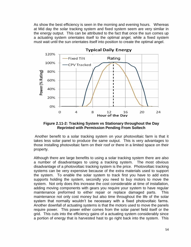
54
As show the best efficiency is seen in the morning and evening hours. Whereas at Mid day the solar tracking system and fixed system seem are very similar in the energy output. This can be attributed to the fact that once the sun comes up a actuating system orientates itself to the optimal angel, while a fixed system must wait until the sun orientates itself into position to create the optimal angel.
Figure 2.11-2: Tracking System vs Stationary throughout the Day Reprinted with Permission Pending From Soltech
Another benefit to a solar tracking system on your photovoltaic farm is that it takes less solar panel to produce the same output. This is very advantages to those installing photovoltaic farm on their roof or there in a limited space on their property. Although there are large benefits to using a solar tracking system there are also a number of disadvantages to using a tracking system. The most obvious disadvantage of a photovoltaic tracking system is the price. Photovoltaic tracking systems can be very expensive because of the extra materials used to support the system. To enable the solar system to track first you have to add extra supports holding the system, secondly you need to buy motors to move the system. Not only does this increase the cost considerable at time of installation, adding moving components with gears you require your system to have regular maintenance preformed to either repair or replace damaged parts. This maintenance not only cost money but also time throughout the life of the solar system that normally wouldn‟t be necessary with a fixed photovoltaic farms. Another downfall of actuating systems is that the motors used to move the panels require power. This power either comes from the solar panel field itself or the grid. This cuts into the efficiency gains of a actuating system considerably since a portion of energy that is harvested hast to go right back into the system. This

55
might be the single most reason that people decided to no actuate there photovoltaic farm.
2.11.2b NON-ACTUATION: The main advantage of non-actuation is cost. The initial cost of a system without actuation is much less than that of a actuation system. The first extra cost you have to consider is the extra support the system will need. Not only does this drive up the cost of installation but it also increases the cost of material to mount to solar array. After buying most support to mount the system you have to buy one or two motors in order to move the system. On top of buying the motors you need to also buy specialized brackets to mount the solar panel on the actuating motors. On top of the extra supplies you need to purchase in order to handle the panels moving you need to add extra maintenance for the whole system. With more moving parts in the design there is more a chance for error and more maintenance to compensate for this. Also there are sensors that need to be maintained. Other than the cost of the non-actuation there are many disadvantages when dealing with the output of your system. First the efficiency of each solar panel is less. This makes it so that your entire system needs to be larger in order to get the same power out. If you are designing a system in limited space, actuating may be the only way to obtain the desired output. Also without actuating your panels are only at a optimum angel at one time throughout the year. This is because the suns pitch in the air. Figure 2.11.3 shows the suns arc and how it changes at different parts in the year.
Figure 2.11-3: Solar arc through sky at different times of the year Reprinted with Permission from

56
The difference in angel changes by thirty degrees through the year if you were to keep the optimal angel for solar radiation. Without your panels having the ability to track the sun your solar array is only receiving the optimal amount of solar radiation for 1/3 of the year. This also affects the solar panels on the day to day basis since when the sun comes up in the morning and sets in the evening it is not at an optimal angel for the panels.
Actuation Non-Actuation
Efficiency High Medium
Cost High Medium
Amount of Time in Optimum Position to the
Sun High Low
Maintenance Medium-High Low
Feet per Watt Low Medium
Support needed to Mount High Low
Energy Returned to System
Medium None
Table 2.11-1: Comparing Actuating vs Non-Actuating Solar Arrays
For this project our team decided to us non actuation. We chose non actuation for many reasons, the first of which was the price. For this project UCF asked for a relatively fair priced solar panel array. Using actuation would have driven the price of the finished array well above budget because of the extra support and equipment needed to actuate the system. Also room was not a factor in this project, as UCF has almost unlimited land to build the solar field.. So the final product didn‟t need to take advantage of the less square footage per what actuation provides. The third and equally important reason we decided to go against actuation is because of the maintenance. If UCF did go on to build a 18 acre solar panel field the maintenance on a actuation solar field that size would be very high. With thousands of motors and moving parts to maintain and replace when needed actuation wasn‟t a real option for our system.
2.11.3 MOUNTING SYSTEM DESIGNED BY
MECHANICAL ENGINGEERS
The mounting system has been the job for the mechanical engineers. Initially
they came up with three different mountings. But after budget and sturdiness,

57
they suggested one mounting system and fortunately it turned out to be the best
mounting to go with our connectivity. The chosen mounting system will carry 12
panels and is build to last in all weather extremes. The mounting system is
shown in figure 1. As we can see, it has low clearance which makes it much
more solid on the ground.
Figure 2.11.3-1: Approved Mounting System
The two mounting system which weren‟t chosen has their drawbacks and
actually will cost more money to build. Since we will be building a solar farm, our
prototype has to pass for the best one. These two mounting systems are shown
in figure 2.
Figure 2.11.3-2 – Rejected Mounting Systems

58
2.12 FPGA VS MICROCONTROLLER:
2.12.1 FPGA CHIP: A FPGA chip (Field programmable gate array) is designed using an integrated circuit so that it can be configured by the consumer after manufacturing. They contain programmable logic which are called “logic blocks” that are wired together. These logic blocks are what give the FPGA chipits flexibility as they can be configured to perform complex functions are simplistic logic gates. Advantages: There are a couple advantages to a FPGA chip over that of a microprocessor that a consumer should take into consideration before deciding how to design their system. The main advantage of a FPGA chip is the fact that you can configure the chip in the field to fix bugs. This is a huge advantage as the chip does not have to be tested and designed in a lab which takes valuable man hours away from testing the actual system as a whole. With the ability of fixing bug in the field you can also use FPGA boards away from the office or lab in which the debugging software and testing equipment. Also another advantage of FPGA boards is that they include shorter time to market. This is very useful as you can design and build a system with a lot less down time in choosing the right microcontroller for the job. On top of having faster times to market FPGA boards also show that less non-recurring engineering is needed. This not only reduces man hours used on the system, it also cuts down the cost of designing and building the system. Xilinx has also claimed several market and technology dynamics that are changing. These trends are changing the way FPGA and microcontrollers have been viewed making FPGA chips look as the better alternative than that of a microcontroller for a larger number of higher-volume applications. The first change is the cost of integrated circuit is increasing as a very aggressive rate. Second is the complex design of a microcontroller on average lengthens the time of development. This is amplified by the fact that more companies are reducing their research and design resources and headcounts. This makes the development time of a FPGA board or Microcontroller board even more important. A forth trend that is increasing the higher number of FPGA chips used over microcontrollers is that the revenue losses due to slower time to market is increasing. With this poor economic time more companies are reducing cost while trying to maximize revenue. This is driving the low-cost technologies such as FPGA boards. Another benefit to a FPGA board is that some of them come with the ability to partially reconfigure them. This is very useful when a design needs to be change a little. Using a FPGA board you can reprogram part of the FPGA chip while leaving other portions of the chip continue running. On top of cost and reprogram ability being major benefits of a FPGA chip they can with stand harsh environments with operational temperatures from -40 to 85 degrees C. This is increases the

59
advantages of FPGA chips into the field where they take more advantages of their field programmability. Disadvantages: Although having many cost, and design/testing benefits FPGA chips are not preferred for every situation. The main disadvantage is the slow processer speed. FPGA chips are less optimized when compared to microcontrollers, this leads to slower data rates. Studies have shown that FPGAs require 18 times more area to design than that of a microcontroller. Also they draw close to 7 times more dynamic power, and can be clocked up to 3 times slower. These differences in data rate and area needed, will always limit FPGA boards in terms of high volume applications, where microcontrollers have excelled in. FPGA chips also do not offer analog functions on the chip, this is a serious downfall to FPGA chips when developing a system using analog signals. Lastly FPGA chips are limited with the fact that they cannot do dynamic logic.
2.12.2 MICROCONTROLLER CHIP: A microcontroller also called a ASIC (application-specific integrated circuit) is an integrated circuit that is customized to meet a particular use, rather than general purpose use. Advantages: When comparing microcontroller to FPGA chips there are many intriguing advantages. The first of which is that microcontrollers use less power than FPGA boards. This makes FPGA chips unsuitable for applications where the loss of power that is used to power them is unacceptable. On top of microcontrollers using less power to run they are more easily set up to handle a certain task. This is due to the fact that when setting up a FPGA board all the code must be written from scratch, then converted to machine code to be executed. While microcontrollers have code that is pre-written to perform special tasks, this reduces the programming overhead that microcontrollers require. Also microcontrollers offer huge advantages to companies when dealing with mass production. This is why FPGA boards are usually only seen in products that have a high degree of complexity but a relatively low demand on the market. Other added benefits of microcontrollers over FPGA chips are that they have analog functions on the chip. This benefit is increased in analog designed systems but also offers flexibility to use digital and analog signals on one chip. Also microcontrollers can do dynamic logic, increasing the ability for them adapt to more designs. Disadvantages:

60
Microcontrollers although being faster than FPGA boards also lack the speed hardware gives you. This is only evident when trying to reach speeds in the few microsecond range. Also microcontrollers cannot be partially programmed while the rest of the chip is not affected. Also FPGA hold a distinct advantage with the ability to process two completely different digital systems that are executing in parallel. This is a ability that microcontrollers lack as they would need two microcontrollers present to run this same systems, one microcontroller for each digital system. In table @@ below we can see the advantages and disadvantages of FPGA boards compared against microcontrollers.
Microcontroller FPGA
Speed High Medium
Cost Low Medium
Analog Functions On chip None on chip
Running multiple digital systems
Unable to do Can run multiple digital
systems cocurrently
Area needed Low Medium
Power consumed Low High
Mass production price Low High
Reprogramability None High
Table 2.12-1: Comparing FPGA and Microcontrollers
CHAPTER 3: DESIGN
3.1: OVERALL DESIGN DECISIONS: For the overall design of our monitoring system there were many curial decisions that had to be made. Below in the block diagram below you can see the full design our team came up with to monitor the solar panels.

61
Figure 3.1-1: Block Diagram Outlining entire Design The first part of our design was determining if we need a secondary small micro controllers located at each panel respectively. This affected our design because the signal sent from this microcontroller would be digital instead of analog. This presented a problem because we are monitoring 12 solar panels respectively. Because of that we would have 24 digital signals split into 12 receive and 12 transmit in total. To make this approach work we would need to choose a microcontroller with 24 digital serial I/O pins all be programmable. This seriously limited us on the brand and type of microcontroller we could choose when design the main PCB board. However if we did not include separate microcontrollers on each panel we could end 3 analog signals from our PCB boards. The three analog signals would be sent to the main PCB board with each one representing one of the variables that we are monitoring. For this project we will be monitoring temperature, current, and voltage of each panel. If we decided to send three analog signals from our PCB board at the panels we would have to make 1 addition to our main PCB board. This addition would be 3 16:1 multiplexers. These three multiplexers would make it possible for us to use a microcontroller with 3 A/D pins instead of finding a microcontroller with 36 A/D pins. This is a major benefit to using analog systems since a microcontroller with 3 A/D pins is a lot cheaper. It also allows us flexibility as having to mane A/D pins would not hurt the design, where as not having enough A/D pins would destroy the design. Another choice after choosing the type of signal we wanted to send from the PCB

62
board located at each panel to the main PCB board is how to send the signal. The two options we could choose would be to send the signal from each panel wirelessly or wired connection. The advantages of sending a wireless signal is it would make the system as a whole cleaner with no wires running along the length of the solar array. However designing a wireless system complicated the design. Since wireless signals are invisible it would be hard to debug, and test the system. Plus with 12 different wireless transmitters all fighting for the same receiver located at the main PCB board a lot of noise will be located in the air. This can make setting up and testing the wireless system a very time consuming and frustrating process. However if we use RJ45 wires to transmit our signal from the secondary PCB boards to the main PCB board we could control where every signal we were sending is going. This would simplify debugging the system in many ways. On the downside is not done right having 24 wires running down the solar array could become messy. For our project it was determined that we would chose to send the information from our secondary PCB board to the main PCB board using a analog signal down a RJ45 cable. This choice was made because we wanted to have the flexibility to choose from a wide range of microcontrollers while also have more control over debugging the monitoring system. We also felt that by not using separate microcontrollers at each panel we would cut down on total cost. After deciding on what signal we wanted to send and how to send it, our group decided to design the PCB board that would be located at each panel. With the ever present requirement of monitoring the voltage, current, and temperature we started to design. First we decided to use a Hall Effect current sensor before the wire was split. This will enable us to get a true current reading of what is coming out of the solar panel. We cannot use a current sensor mounted onto the board because we will use a Op-Amp to block the current from running through the board. This would block the current from running through a current sensor on the board leaving us with a useless reading. Once the hall effect sensor is connected we will connect the wire to the PCB board so that we will be able to send its reading through the RJ45 cable to the main PCB board. After the current sensor we will have a three stage terminal block. This will allow us to connect with the wire in order to obtain the voltage of the solar panel. Once the wire is connected from the terminal block it will directly connected to out PCB board. The positive terminal will first travel over a 27K resister while the negative side will travel over a 5K resister. Once both terminals have passed their respective resistors they will be connected to feed into the positive side of a Op-Amp. The output of the Op-Amp will then me wrapped back around to the negative side and also to our RJ45 cable. Lastly we will use a surface mounted temperature sensor to obtain the temperature of the solar panel. This wire will also be connected to the PCB board so that it can be sent through the RJ45 cable as well. The schematic for this board can be seen below in figure 3.1.2.

63
Figure 3.1-2: PCB Board at the Panel Design
Once each of the PCB are made for the panels we will transfer their signals through 12 RJ45 cables, one for each panel. The RJ45 cables were chosen by our group because of their flexibility. RJ45 cables consist of 8 separate small wires twisted together. These wires are insulated and do not touch each other within the RJ45 cable. Because of this you can send eight different signals down a RJ45 cable. With three signals coming from the PCB board at the panels to the main PCB board, plus the VCC and ground of the sensors, a cable with the ability to transfer 8 signals was ideal for this project. Once all twelve RJ45 cables are plugged into the main PCB the real design begins. In instead of using a microcontroller with 36 A/D pins which would be very expensive we decided to insert all the inputs into 3 16:1 multiplexers. Each one of these multiplexers would receive the same input from the RJ45 cables. So all 12 voltage readings would be plugged into one multiplexer, all 12 current reading signals would be plugged into the second multiplexer, and all 12 of the temperature reading would be sent to the third multiplexer. Once we have the multiplexers set up we need to connect each one to a A/D pin on our microcontroller. This allows us extreme

64
flexibility of choosing the micro controller since many of them have 3 or more A/D pins. Figure 3.1.3 shows the design we created for the main PCB board.
Figure 3.1-3: Main PCB board schematic Design
After designing the Main PCB board our group turned our attention to how to transmit the information from the main PCB board to a computer with a internet connection. To accomplish this we decided that a wireless signal is the only way to go about doing this since the distances we would have to run wires is very large. After deciding how we were going to send we started looking into the wireless technologies that we would need in order to accomplish this objective. After doing research on the three wireless technologies (Bluetooth, WiFi, and ZigBee) we decided that ZigBee was the best option for us to design our wireless system. This decision was made because the ZigBee data sheet showed that a XBee-Pro was the only wireless technology with the range that would accomplish the distance we were trying to send our wireless signal. Once we are transmitting the wireless signal to a computer with internet connection we can

65
develop a website with the information obtained from the solar panels. This would be very beneficial for the university since it will be able to demonstrate to the public their ability and willingness to go green. This would increase interesting in renewable energy plus create a better public image. On this website our team will demonstrate how many other fossil fuels would have been burned in order to produce the same amount of energy as the solar field. The website will also be designed to show the power output of the solar array at different times of the day and different times the year.
3.2 MONITORING SYSTEM DESIGN: The solar panel monitoring system that is being designed for the photovoltaic farm needs to be built for accuracy and longevity. This part has to be designed as cheap as possible with the thought of a twenty year life span. On average the typical solar panel has a twenty year life span so to be as cost effective as possible only parts with equal or near equal life spans will be considered for this assignment. There are a lot of considerations that need to be made at every phase of the monitoring system like:
Design Considerations
Types of Voltage Sensors Voltage Divider Network
Op-Amp (LF351)
Types of Resistors Carbon Composite Resistors
Carbon Film Resistors
Types Of Zener Diodes
Power Dissipation Operating Temperature
Nominal Voltage
Operational Amplifiers Unity Gain
Operating Temperatures
Board to Board Communication Wi-Fi RJ 45
Types of Microcontrollers
Number of A/D Pins Surface Mount or Through Hole
Number of Bits of Accuracy Operating Temperature
Power Supply
Power From The Solar Array Battery
Small Solar Panel
Communication
Wi-Fi Blue Tooth Hard Wired
Table 3.2-1 Design Considerations

66
3.2.1 VOLTAGE SENSORS:
When it comes to selecting the appropriate sensors for this assignment it has been discovered that there exists a plethora of different types of sensors. So narrowing down the choices has proved to be quite difficult. The types of voltage and current sensors that are under consideration for the final design are onboard surface mount sensor chips and hall effect sensors that can be placed at the solar panels themselves.
3.2.1.a VOLTAGE SENSING:
A solar panel for this project produces has a maximum output voltage of 32V. This much voltage is immeasurable by the microcontroller that is question for the monitoring system. To manage the voltage reading a voltage divider circuit will have to be used to step down the incoming voltage from the individual solar panels to something reasonable like 5V. Most microcontrollers have a swing voltage that they can operate within and the PIC18 series of microcontrollers have a low drop out voltage of 3.3V while the I/O pins can withstand a voltage of up to 5.0V. The drop out voltage is a parameter built into the device that tells the device when to turn on and off. Of course all of these parameters are not specific to all of the microcontrollers within the PIC18 series family but they are good general reference numbers for the ultimate design of the monitoring system. The values for the resistor in the voltage divider network are calculated using equations 2.4-1 and 2.4-2. An example of the type of calculation has been provided below.
For the circuit in question here the values for R1 and R2 have been calculated to be 27kΩ and 5kΩ respectively.

67
Figure 3.2-1 This is a basic circuit but it is a very effective circuit in performing the task of stepping the voltage down. The max voltage rating is always going to be 32V for the panels selected for this project but the input parameters for the PIC may change depending on the one selected. The resistors will simply be adjusted to accommodate this change.
3.2.2 RESISTORS: The next thing to consider would be the resistor because all resistors are not the same. The resistors for this project need to be selected carefully due to the nature of the environment that the will be subjected to. The environment in Florida is very consistent in that it will never reach below freezing and stay there for a long period of time but there are big swings in the temperature from season to season. During the summer the temperature in Orlando Florida can reach a temperature as high as 92.1°F and during the colder months the temperature can drop as low as 50.0°F. This is not a huge swing in temperature but when dealing with electronic parts like resistors these parameters need to be taken into account because they will affect the overall performance of the system. A chart can be seen below in Figure 3.2.2 showing the weather condition for the UCF area over the course of a year.
To Op Amp &
A/D input pin
Solar Panel (VIN)
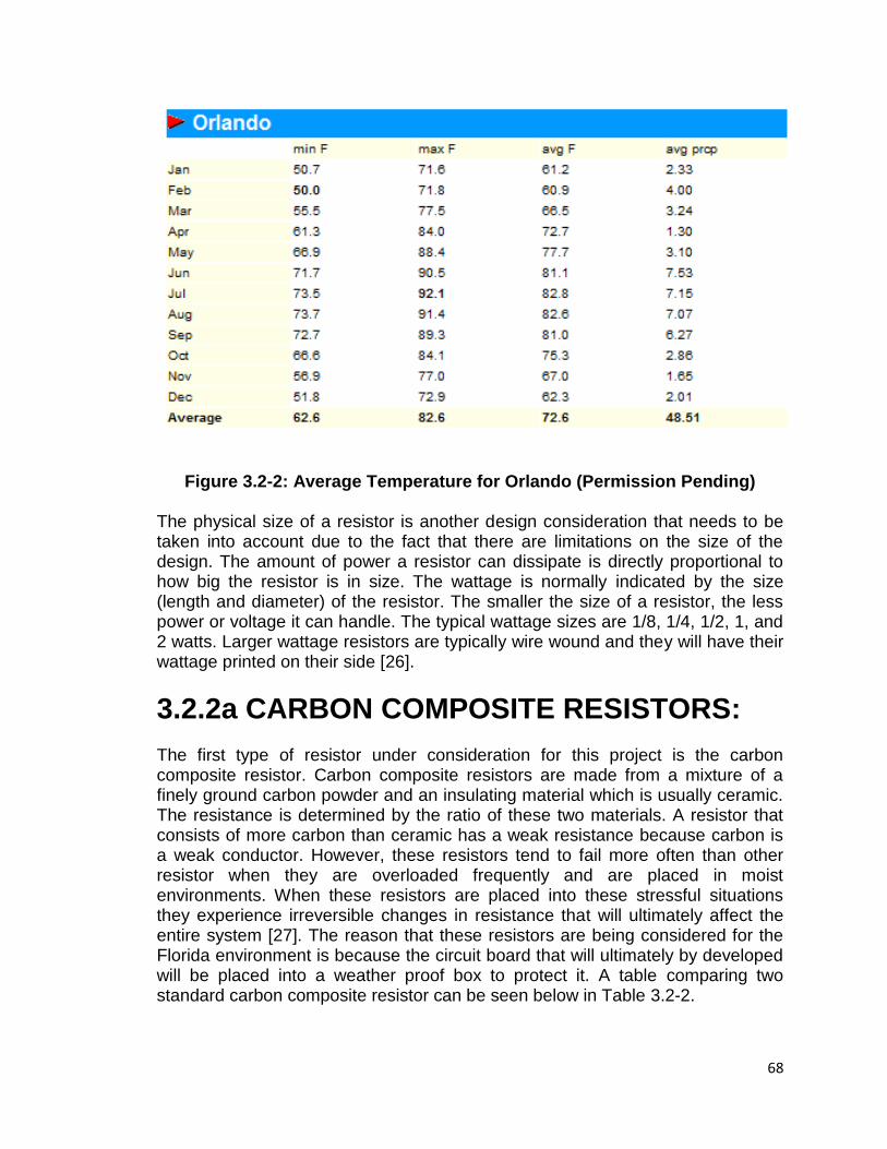
68
Figure 3.2-2: Average Temperature for Orlando (Permission Pending) The physical size of a resistor is another design consideration that needs to be taken into account due to the fact that there are limitations on the size of the design. The amount of power a resistor can dissipate is directly proportional to how big the resistor is in size. The wattage is normally indicated by the size (length and diameter) of the resistor. The smaller the size of a resistor, the less power or voltage it can handle. The typical wattage sizes are 1/8, 1/4, 1/2, 1, and 2 watts. Larger wattage resistors are typically wire wound and they will have their wattage printed on their side [26].
3.2.2a CARBON COMPOSITE RESISTORS: The first type of resistor under consideration for this project is the carbon composite resistor. Carbon composite resistors are made from a mixture of a finely ground carbon powder and an insulating material which is usually ceramic. The resistance is determined by the ratio of these two materials. A resistor that consists of more carbon than ceramic has a weak resistance because carbon is a weak conductor. However, these resistors tend to fail more often than other resistor when they are overloaded frequently and are placed in moist environments. When these resistors are placed into these stressful situations they experience irreversible changes in resistance that will ultimately affect the entire system [27]. The reason that these resistors are being considered for the Florida environment is because the circuit board that will ultimately by developed will be placed into a weather proof box to protect it. A table comparing two standard carbon composite resistor can be seen below in Table 3.2-2.

69
IBT 1/4 IBT 1/2
Power Rating Determined by load life test 100% load @ 70°C
ambient
¼ W
½ W
Rated Continuous Working Voltage
(RCWR)
P x R or 250V
Whichever is less
P x R or 350V
Whichever is less
Maximum Ambient
Temperature
±130°C
±130°C
Nominal Resistance
Range
1Ω - 5.6MΩ
1Ω - 20MΩ
Resistor Tolerance
± 5%, ±10%
± 5%, ±10%
. Table 3.2-2: Comparing the IBT ¼ and the IBT ½
3.2.2b CARBON FILM RESISTORS:
The second resistor under consideration for this project is a carbon film resistor. A carbon film is deposited on an insulating substrate, i.e. silica, CaF2, or Al2O3, and a helix is cut into it to provide the current with a long narrow resistive path. Varying the shape along with the resistivity of carbon can provide a variety of different values of resistance. These resistors are available in a range that is from 1Ω to 10MΩ. One of the nicest features about this type of resistor is the operating temperature range. This type of resistor has an operating temperature that ranges from -55°C to 155°C which is very conducive to the Florida temperature ranges. Below in Table 2.4-3 a caparison can be seen between two different carbon film resistors from the Vishay Corporation.

70
LCA0204 / SK1 LCA0207 SK2
Power Rating Determined by load life test 100% load @ 70°C
ambient
¼ W .35 W
Rated Continuous Working Voltage
(RCWR) 200V 350V
Maximum Ambient Temperature
±155°C
±155°C
Nominal Resistance
Range
1Ω - 1MΩ
1Ω - 5MΩ
Resistor Tolerance
± 2%, ±5%
± 2%, ±5%
Table 3.2.3: Comparison of Two Carbon Film Resistors
3.2.2c Wire Wound Resistors: The next resistor under consideration for this project is the wire wound resistor. Wire wound resistors are made from winding a metal wire, usually nichrome, around a ceramic, plastic, or fiberglass core. The ends of the wire are then soldered or welded to two caps or rings that are attached to the ends of the core material. The resistor is then protected by a layer of paint, molded plastic, or an enamel coating which is baked at a high temperature. This makes these resistors able to withstand very high temperatures, up to +450°C. The wire leads of the resistor range in diameter from 0.6 mm to 0.88 mm and are coated with tin to aid in the soldering process. Below in Table 2.4-4 are two cemented wire wound resistors that are produced by the Vishay Corporation. These resistors are made with welded construction, ceramic core, non-flammable cement coating, tinned copper-clad iron leads (for axial parts), high power dissipation in a small volume, ideal for pulse applications, lead (Pb)-free, and compliant to the RoHS directive 2002/95/EC. The Vishay Corporation makes a lot of electronic parts for the military with their intended use to be in military applications. There price is pretty comparable to similar products on the market and being that there product is used in military an application that says a lot about the quality and reliability.

71
AC07 AC10
Power Rating Determined by load life test 100% load @ 70°C
ambient
5.8 W
8.4 W
Rated Continuous Working Voltage
(RCWR)
Maximum Ambient
Temperature
Not Listed
Not Listed
Nominal Resistance
Range
1.6KΩ - 15KΩ
620Ω - 27KΩ
Resistor Tolerance
±5%
±5%
Table 3.3.4: Specification for Wire Wound Resistors (Permission Pending)
3.2.3 VOLTAGE DIVIDER/RESISTOR CONCLUSION: The voltage divider circuit discussed above is an essential part of the design plan. The voltage from the solar panels is simply too high to be measured by the microcontroller. The input voltage of the microcontroller is still in question so the value of the resistors that were calculated was just an example of the type of logic that is going to be used when calculating the resistors. The three resistors that were discussed were the carbon composite resistor, the carbon film resistor, and the wire wound resistor. By examining what the data tells us for each resistor a decision can be made about which one to use. The carbon composite resistor fits this application well if a suitable weather proof box can be found to keep moisture from building up on the circuit. The carbon film resistor also fits this application well because of its ability to operate in a wide range of temperature but the cost of using them versus the wire wound resistor makes it unreasonable because of the scale of the project. The wire wound resistors are the most appealing to this design because of the durability, operating temperature range, cost, and reputation. So, the wire wound resistors are the resistors that will be selected for this project. Whether they are purchased

72
from the Vishay Corporation or not will be determined by the availability of the part.
3.3 ZENER DIODES:
Another important aspect to the design of the prototype is going to be to protect the microcontroller from spikes in voltages. Spikes in voltages could be caused by lightning strikes, electrostatic discharge (ESD), or the solar panels operating outside their maximum voltage range. A zener diode will be placed in parallel with the microcontroller so to regulate the incoming voltage to no greater than 5.1V in case of a voltage spike. The design for this voltage regulator can be seen below in Figure 2.4-3 and the voltage characteristics of the 5.1V zener diode can be seen in Figure 2.4-4.
Figure 3.3-1: Voltage Regulator
Figure 3.3-2: Current vs Voltage Characteristics (Permission Pending)
5.1 V Zener
for
Protection
73
The microcontroller has a tolerance of slightly more than 5V so a 5.1V zener was selected for the design so that the input voltage can have a chance to meet its full potential and not be truncated as soon as it reaches 5V. There are several types of zeners on the market today. They come as surface mount chips or through hole parts. For this design a through hole mounted part will be selected due to the simplicity to mount these types of diodes and the flexibility of being able to remove the diode form the board and replace it if it is faulty. The part that was selected for this was the 1N5333B Series 5 Watt Surmetic_40 Zener Voltage Regulators made by ON Semiconductor. This part was selected because it has a tight limits and better operating characteristics that reflect the superior capabilities of silicon-oxide passivated junctions [28]. Some of the operation characteristics can be seen below in Table 2.4-5.
Zener Diode Operation Characteristics
Max Steady State Power Dissipation @ TL = 75 °C
5W
Operating and Storage Temperature Range
-65°C – 200 °C
Zener Voltage Range -3.3 V – 200 V
ESD Rating >16kV
Surge Rating 180 W @ 8.3 ms
Lead (Pb) Free Packages are Available
Table 3.3-1: Zener Diode Operation Characteristics
3.4 OPERATION AMPLIFIERS: The next part of the design to be considered is the use of an operational amplifier. Operational amplifiers are needed for this prototype because all of the data is going to be encoded as a voltage and sent through a RJ 45 cable to a central location. Getting the data from the solar panel monitoring system to this central data acquisition board is a very important aspect to the design and operational amplifiers will aid in the process. There are many types of operational amplifiers but the one to be considered for this design is the unity gain op-amp. Unity gain is the term given to this kind of circuit design because the overall gain of the circuit is unity. This is important because we don‟t need to add any gain to the output, if there was any gain to be added to the output another circuit would have to be devised at the receiving terminal of the data acquisition board to step the voltage down again.

74
Operational amplifiers are important building blocks for a wide range of electronic circuits. The operational amplifier has “ideal characteristics” like zero input offset voltage, infinite slew rate, zero output impedance, and zero noise. These characteristics are unrealizable in actual circuits but they explain why the op-amp is a good choice for this application. For example when sending a voltage a long distance through a cable excessive noise in the line will produce false outputs voltages at the input terminal of the data acquisition board. So, by using an op-amp after the voltage divider and zener diode in the prototype the noise on the input terminal of the data acquisition board will not be eliminated, because nothing is ideal, but it will be drastically reduced. An example circuit with the operational amplifier in place can be seen in Figure 2.4-5.
Figure 3.4-1: Prototype with Op-Amp There are several different amplifiers on the market including LM392 Low Power Operational Amplifier/Voltage Comparator by National Semiconductor and the TLV2302 by Texas Instrument. Both of these devices have the desired operating characteristics for this project and fall within the budgets means. These characteristics can be seen below side by side in Table 3.4-1.
LM392 TLV2302
Input Off Set Voltage ±5V ±5V
Operation Temperature 0°C - 70°C -40°C - 125°C
Input Offset Current ±5 nA 25 pA
Table 3.4-1: Comparison of Two Op-Amps Being Considered

75
The LM393 is going to be the operational amplifier that is selected for this prototype because it is slightly cheaper than the TLV2302 operational amplifier and it has more than enough capability to achieve the parameters set out by the designers.
3.5 CURRENT SENSORS: The choice of the type of current sensor to use for this prototype design has been the most difficult thus far. There are several different approaches that have been considered thus far including a surface mount Hall Effect sensor with dc analog output (ACS712ELCTR-20A-T), a Hall Effect current sensor clamp (CR5410-20), and an open loop current sensor (CSLT6B100). Like the resistors these components can get bulky by electronic standards and we need to stay low profile and reliable for long term measurements.
3.5.1 ACS712 CURRENT SENSOR: The first current sensor that is under consideration for the prototype design is the PCB mounted, low profile ACS712ELCTR-20A-T current sensor. This is a surface mount eight pin device that requires a 5V input voltage and produces a analog output voltage that is a measure of the induced current. Being that this is a surface mount Hall Effect device the current is measured by passing a current underneath the sensor in a copper trace or over the top of the sensor inside a wire. In some situations it may be desired to improve the accuracy of the sensing unit and this can be achieved in low frequency applications by adding a simple RC filter. Such a low pass filter improves the signal to noise ratio and therefore the resolution of the output signal. However the addition of an RC filter to the output of the sensor IC can result in undesirable device output attenuation [29]. A typical application for ACS712 current sensor can be seen in Figure 2.4-6. If this current sensor is chosen for the prototype, a similar circuit design will probably be used to get the data to the A-to-D converter on the microcontroller. The noise reduction circuit that was discussed above will probably also be used depending on the amount of noise in the line. The characteristics of the current sensing device can be seen below in Table 2.4-7.

76
Figure 2.5-1: Typical Application with Current Sensor (Permission Pending)
ACS712
Supply Voltage 4.5V – 5.5V
Supply Current 10 mA
Current Measured 0 – 20 A
Operating Temperature -40°C - 85°C
Sensitivity 185 mV/A
Power On Time 5 µS
Table 3.5-1: ACS712 Characteristics
3.5.2 CR5410-20 CURRENT SENSOR: The next current sensor under consideration for the prototype is the Hall Effect current clap sensor CR5410-20. This device is a split sore Hall Effect sensor that clamps around the outside of a wire which allows designers more flexibility in the placement of the sensor. The installation of this devise should prove to be much easier than the surface mount sensor because it can be mounted without having to solder pins to a PCB or have require any complicated circuitry to guarantee

77
the accuracy of its output. The dimension of this device can be seen below in Figure 2.4-7 and the general characteristics can be seen below in Table 2.4-8.
Figure 3.5-2: Dimensions of the Hall Effect Sensor (CR5410-20)
CR 5410-20
Supply Voltage N/A
Supply Current N/A
Current Measured 0 – 20 A
Operating Temperature 0°C - 60°C
Sensitivity High Sensitivity
Power On Time 200 µS
Table 3.5-2: Characteristics of the Current Sensor CR 5410-20
3.5.3 CSLT6B100 CURRENT SENSOR: The next current sensor that is under consideration for the prototype design of this project is a miniature open-loop current sensor. The sensor is produce by the Honeywell corporation and it posses many characteristics that make it the suitable choice for this project. It has wired open-loop design with multiple turns for increased sensitivity, it senses as or dc current, has a fast response time, is

78
compact in size for applications with a limited amount of space, is very accurate for a low cost, has an operating temperature that ranges between -13°F to 212°F and is RoHSs compliant. Some of the typical application for this current sensor include but are not limited to current monitoring in electrical circuits, over current protection, ground fault detectors, robotics, and battery management systems in mobile equipment. The scope of this project is to measure the current in an electrical circuit so it fits right in with what we are trying to do. The characteristics of the sensor are summed up below in Table 2.4-8.
CSLT6B100
Sensor Type Open Loop Linear
Sensed Current Type ac or dc
Sensed Current Range ±100 AT
Package Style PCB Bottom Mount
Sensitivity 15 mV/AT min. to 19 mV/AT max.
Supply Current 9 mA max.
Supply Voltage 4.5 Vdc to 10.5 Vdc
Response Time 3 µs
Operating Temperature -13 °F to 212 °F
Mounting PCB on 3 pins
Table 3.5-3: Characteristics of CSLT6B100
One of the characteristics of this device that make it the most attractive is the size of the device. The wire size that the solar panels selected for this project require is 12 AWG which has a circumference of 3 mm2. The opening of the CSLT6B100 Hall Effect sensor measures 5.2 mm which allow for plenty of room for the design. The overall dimensions for the CSLT6B100 can be seen below in Figure 2.4-8.

79
Figure 3.5-3: Dimensions for the CSLT6B100 (Permission Pending)
The three current sensors that are in question above are all good choices for this project but only one will be selected. The ACS712ELCTR-20A-T that was discussed above is a great choice for this project but because it is a surface mount part it will be difficult to change the part if it malfunctions in anyway. The CR5410-20 is another good choice but it is a lot bigger than the desired specs call for and at a hundred and five dollars for one unit it would prove to be a very expensive choice. Finally, the CSLT6B100 proves to be the best choice for the prototype. It is a through hole mount device that requires only 5V of supply voltage that is extremely accurate and at a price of $6.75 it look the most economical.
3.6 TEMPERATURE SENSOR: The desirable quantity that needs to be acquired for this project is the temperature of each panel. This is a very important quantity because as solar panels rise in temperature their efficiency drops significantly. By collecting this data a calculation for each solar panel‟s efficiency can be done so that design considerations can be made in later projects of similar scope. The placement of

80
the temperature sensor is a key part of the design because we do not want to measure the ambient temperature of the air surrounding the solar panels. We want to measure the temperature directly on the solar panels so a surface mount temperature sensor is the ideal device that we need.
3.6.1 WE710 TEMPERATURE SENSOR: The first temperature sensor that was examined for this project was the WE710 surface temperature sensor produced by the Global Water Instrumentation Corporation. Some of its key features are listed below in Table 2.4-9.
WE710 Operating Characteristics
Sensor Type 100ohm Platinum Class A RTD
Output 4-20 mA
Temperature Sensing Range -58°F to 185°F
Accuracy ±0.5°F
Operating Voltage 10-36 Vdc
Warm Up Time 3 seconds minimum
Cost $295.00
Table 3.6-1: WE710
3.6.2 CS220 TEMPERATURE SENSOR: The second temperature sensor that is being considered for this project is the CS220 that is produced by Campbell Scientific. The CS220 surface-mount thermocouple was made to measure the temperature on the back of a solar panel. The CS220 simply adheres in the center of the back panel of a solar module. The thermocouple posses a self adhesion backing so that once the location for mounting is determined the area could be cleaned and the thermo couple is attached right to the back of the panel. From the thermocouple a stainless steel over braided cable extended which is connected to a mini connector that attaches the thermocouple to the thermocouple extension cable. Then the pigtail connector at the end of the wire extension can be connected to the secondary printed circuit board so that the measurement can be made. The way that the thermocouple works is that a voltage potential is generated when the “measurement end” of the thermocouple is at a different temperature than the “reference end”. The magnitude of the voltage potential is related to the temperature difference of the two end of the thermocouple. The typical output of

81
voltage is 60µV/°C. The only drawback with this sensor is it is $75.00 but it seems that all of temperature sensors on the market are rather expensive.
3.6.3 SA1-RTD TEMPERATURE SENSOR: The final temperature sensor that is under consideration for this project is the SA1-RTD temperature sensor. This is a self adhesive or cement on surface mount device that is cheaper than the previous two. The SA1-RTD surface mount temperature sensor mounts on flat or curved surfaces and provides a high point of accuracy for critical temperature monitoring applications. The operational characteristics of the SA1-RTD can be seen below in Table 2.4-9.
SA1-RTD Specifications
Operational Temperature Range -73°C to 260°C
Accuracy ±0.06Ω at 0°C
Stability < 0,2°C Drift/Year
Response Time < 0.9 s
Cost $50.00
Table 3.6-2: SA1-RTD Specifications
All three of the surface mount temperature sensors that are being considered are really similar in the mounting and operation. The deciding factor on this part is going to be the cost. The prices range from $295.00 to $50.00 and with cost being a concern for the developers of the overall system of the three megawatt field, temperature sensors at $295.00 dollars each is unrealistic. Even if the cheapest of the three is used at 50 dollars each just to monitor the temperature on the initial twelve panels is a total cost of $600. So, in this group‟s opinion it would be best to take a temperature reading on three panels and average the three for the efficiency calculation.
3.7 DATA ACQUISITION: There is several different ways that the collected data can be sent to the primary printed circuit board. It can be moved via RJ45 or wirelessly. The ideal situation would be to do it wirelessly to take advantage of not having to run additional wires, but this may prove to be too difficult. RJ45 cabling seems to a technology that has been around for a while and has proven itself in networking application and may prove to be the best solution for this project.

82
3.7.1 RJ45 CABLE/CONNECTION: RJ45 specifies the physical male and female connectors as well as the pin assignments of the wires in a telephone cable. The RJ45 connector is commonly used for network cabling and for telephone applications but it can also be used for serial connections in special cases [29]. The RJ45 that would be used for the proposed prototype design would consist of eight twisted pair wire that would also contain some external shielding. Twisted pair cabling is when two conductors, forward and return are twisted together for the purpose of canceling out and electromagnetic interference which can be produced by unshielded twisted pair cables. This phenomenon is known as cross talk between neighboring pairs and it pollutes the transmitted signal which can render the data useless. Another name for the RJ45 cable connection is known as Cat5 or Cat5E cables. These cables are typically used for Ethernet connections but as it was explained to me “it‟s just a wire and it can be used for what for whatever the designing engineer has intended for it”. Below in Figure 2.4-9 the assembly and layout of the pins can be seen.
Figure 3.7-1: RJ45 Pin Layouts (Permission Pending)
RJ45 seems to be the most logical choice for this project due to the simplicity of its operation. The RJ45 consists of eight wires that are twisted pair and shielded. Wires one and two will be used to transmit the VCC of 5V that is needed to operate all of the parts on the secondary printed circuit board. This voltage will be acquired from a standalone power system that is being designed for the prototype. The VCC will come from the battery with VCC
+ being on wire one and VCC
- being placed on wire two. This pattern will be repeated for all twelve of the RJ45 connections to power the secondary printed circuit boards. Wire three of the RJ45 will be used as the ground connection for all of twelve of the secondary printed circuit boards. Wire four will be used to send the analog voltage output from the secondary printed circuit boards to the primary circuit board. Wire five will be used to transmit the output analog voltage for the CSLT6B100 current
83
sensor to the primary circuit board. Finally, wire six shall be used to transmit the output analog voltage of the temperature sensor back to the primary circuit board. Below in Table 2.4-9 all of the connections can be seen.
RJ45 Wire Definitions
Wire One VCC+
Wire Two VCC-
Wire Three Ground
Wire Four Analog voltage Output of Voltage
Sensor
Wire Five Analog voltage Output of
CSLT6B100 Current Sensor
Wire Six Analog voltage Output of
Temperature Sensor
Wire Seven No Connection
Wire Eight No Connection
Table 3.7-1: RJ45 Connections
3.8 WIRELESS: The other option being considered for this project is to send the data wirelessly form each secondary printed circuit board to the primary printed circuit board. Although this approach seems like it would be a good idea it has proven to be more trouble than it is worth. The computer coding to get all of the wireless signals to be transmitted and received at the proper times seems to be the most difficult part and although nothing is impossible, time is of the essences and this group does not see it logical to get bogged down in weeks of coding and debugging with so many other parts of the project that need to be designed and implemented.
3.9 TERMINAL BLOCK: In order to get the secondary printed circuit board connected to the solar panels to make the voltage and current readings we will need to use a two terminal blocks at each panel. The wire leads form each solar panel will be striped and connected to a single level two position terminal block on either side of the printed circuit board. The terminal block is a through hole pcb mounted device that will distribute the positive and negative voltages through the first position of the terminal block to the measurement devices. Position one and position two of

84
the terminal blocks will be connected in parallel so to send the same voltage out of the measurement pcb to the next panel. In effect the measurement or secondary pcb will be connected in parallel with the incoming and outgoing voltage outputs of the solar panel so to not draw any voltage away from the system causing an unwanted loss. The terminal block that was selected for the prototype design is the Eurostyle Terminal Block 796740 produced and distributed by Tyco Electronics. We will need twenty four of the devices and the cost $1.22 cents each if they are purchased individually. We can receive a price break of .of ~.12 cents per device by purchasing all 24 at once. The operational specification can be seen below in Table 2.4-10 and the dimensions of the device can be seen in Figure 2.4-10.
Terminal Block Type Wire to Board
Number of Levels/Positions Per Level 1 , 2
Mating Orientation Horizontal with Board
Current 30A
Voltage 300V
Wire Gauge 10 – 24
AWG
Mounting Type Through Hole
Table 3.9-1: Eurostyle Terminal Block 796740
Figure 3.9-1: Dimensions of Terminal Block (Permission Pending)

85
The layout of these pieces is a key part to the design of the prototype because if the terminal blocks are not laid out in the proper orientation the wire can become difficult and damage can either be done to the printed circuit board or the wires themselves. The proposed design can be seen below in Figure 2.4-11 and it will need to be tested for functionality in the senior design lab. We will refer to this layout while setting up the prototype and consult with the proper people if design changes need to be added.
Figure 3.9-2: Terminal Block Layout
3.10 MULTIPLEXERS: Now that the data has been transmitted from the measurement equipment down the RJ45 line and to the primary printed circuit board, the data has to be moved to the Microcontroller in an orderly manner. There are several approaches that were considered for this. The first approach was to find a microcontroller with 36 A/D pins that were digitally programmable. This proved to be unrealistic because there is no such part. So, the next option was to .multiplex thirty six analog signals into a multiplexer with three A/D input/output pins. This approach seemed much more logical that the prior because multiplexers come at an abundant source. The ideal situation would be to have thirty six analog signals come from the twelve different solar panel monitoring systems (secondary printed circuit boards) into three sixteen by one multiplexers. With this approach we could take all of the voltage measurements from the voltage regulators into one multiplexer, all of the analog current outputs into another multiplexer, and all of the analog temperature sensor outputs into the last multiplexer. From there all of the coding could be

86
done to set the timing of the multiplexers to read the data in the following manner: Panel 1: Voltage; Current; Temperature Panel 2: Voltage; Current; Temperature Panel 3: Voltage; Current; Temperature….etc………………..
3.10.1 MC14067B ANALOG MULTIPLEXER: There are several different multiplexers under consideration for the prototype. The first is MC14067B analog multiplexer that is produced by ON Semiconductor. The MC14067 multiplexer is a digitally controlled analog switch which features a low ON resistance and very low leakage current. This device can be used in either digital or analog application. The MC14067 is a 16-channel multiplexer with an inhibit and four binary inputs A, B, C, and D. These control inputs select one of sixteen channels by turning ON the appropriate analog switch. The operational features of the MC14067 can be seen below in Table 2.4-11. A diagram for the pin layout can be seen below in Figure 2.4-12.
MC 14067 Multiplexer
Supply Voltage -0.5 V – 18 V
IIN ±10 mA
PD 500 mW
Operating Temperature -55°C - 125°C
Operating Voltage Range 3 V – 18 V
Low Cross Talk Between Channels
Low Noise in the Pins
Table 3.10-1: MC 14607 Multiplexer

87
3.10.2 AS250A ANALOG MULTIPLEXER: The second multiplexer that is under consideration for this prototype is the AS250A one of sixteen multiplexer with 3-State Outputs. This device is produced by Texas Instruments and carries a price tag of $8.63. The AS250A device provides full binary decoding to select one of the sixteen inputs. The selected inputs are buffered with symmetrical time delays to reduce the possibility of transients occurring at the outputs. The AS250A has an operating temperature that ranges from -55°C to 125°C. A buffered output-enable (OE) input can be used for n-line to 1-line cascading. When taking the output enable high, it places the output signal in the high-impedance state, when in the high impedance state the output neither loads nor drives the bus lines significantly. The truth table and pin layout for the AS250A can be seen below in Figure 2.4-12.
Figure 3.10-1: AS250A Truth Table and Pin Layout (Permission Pending)
3.10.3 MPC506A ANALOG MULTIPLEXER: The last multiplexer being considered for the prototype is the MPC506A which is produced by Texas Instruments. The MPC506A ia a 16 channel single ended analog multiplexer that has an input overvoltage protection. “Analog input voltages may exceed either power supply voltage without damaging the device or disturbing the signal the signal path of other channels. The protection circuitry assures that the signal fidelity is maintained even under fault conditions that

88
would destroy other multiplexers. These features make the MPC506A ideal for use in systems where the analog signals originate from the external equipment [30]”. This is a great feature for the type of electronic system that is being designed. Our system will be exposed to the elements out in a wide open field. There will be additional protection element in place such as the zener diode but the added protection of this multiplexer is a welcomed attribute. If an electrostatic discharge happens to get past the zener diode the added protection will aid in protecting the microcontroller from exceeding it maximum rated voltage which would terminate the whole system. The only drawback of this part is that it requires a ±15V supply voltage. This voltage will be able to be provided but it is more than the group planed on providing for these parts. Below in Table 2.4-12 the operational characteristics are listed and the truth table for the part is stated in Figure 2.4-13.
MPC506A
Supply Voltage ±15V
Operating Temperature -55°C - 125°C
Access Time 3 µS
PD 7.5 mW
Table 3.10-2: MCP506A Operational Characteristics
A3 A2 A1 A0 EN “ON”
CHANNEL
X X X X L None
L L L L H 1
L L L H H 2
L L H L H 3
L L H H H 4
L H L L H 5
L H L H H 6
L H H L H 7
L H H H H 8
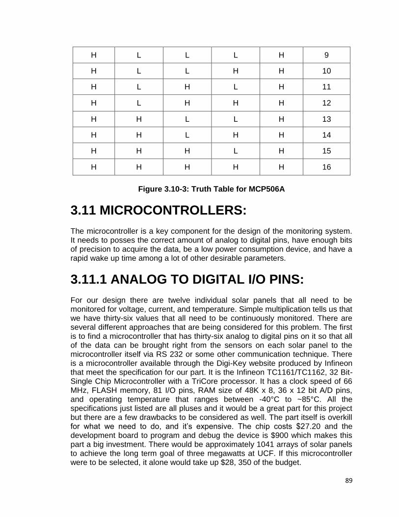
89
H L L L H 9
H L L H H 10
H L H L H 11
H L H H H 12
H H L L H 13
H H L H H 14
H H H L H 15
H H H H H 16
Figure 3.10-3: Truth Table for MCP506A
3.11 MICROCONTROLLERS: The microcontroller is a key component for the design of the monitoring system. It needs to posses the correct amount of analog to digital pins, have enough bits of precision to acquire the data, be a low power consumption device, and have a rapid wake up time among a lot of other desirable parameters.
3.11.1 ANALOG TO DIGITAL I/O PINS: For our design there are twelve individual solar panels that all need to be monitored for voltage, current, and temperature. Simple multiplication tells us that we have thirty-six values that all need to be continuously monitored. There are several different approaches that are being considered for this problem. The first is to find a microcontroller that has thirty-six analog to digital pins on it so that all of the data can be brought right from the sensors on each solar panel to the microcontroller itself via RS 232 or some other communication technique. There is a microcontroller available through the Digi-Key website produced by Infineon that meet the specification for our part. It is the Infineon TC1161/TC1162, 32 Bit-Single Chip Microcontroller with a TriCore processor. It has a clock speed of 66 MHz, FLASH memory, 81 I/O pins, RAM size of 48K x 8, 36 x 12 bit A/D pins, and operating temperature that ranges between -40°C to ~85°C. All the specifications just listed are all pluses and it would be a great part for this project but there are a few drawbacks to be considered as well. The part itself is overkill for what we need to do, and it‟s expensive. The chip costs $27.20 and the development board to program and debug the device is $900 which makes this part a big investment. There would be approximately 1041 arrays of solar panels to achieve the long term goal of three megawatts at UCF. If this microcontroller were to be selected, it alone would take up $28, 350 of the budget.

90
The next option for the monitoring system would be to go with a microcontroller with fewer A/D pins and use multiplexers to feed the information into the system. Using our simple math from above we could use three sixteen to one (16:1) multiplexers and feed the data into a microcontroller that has as few as three analog to digital pins. The programming for this approach would be substantially more difficult than the above approach but senior design labor is free where as twenty eight thousand dollars for a single component is not. So, the microcontroller being considered for the second approach comes from the PIC18 family of microcontrollers and it is user friendly. The PIC18F8722 has 128K bytes of programmable FLASH memory, 70 I/O pins, 16 10-bit A/D pins, is C programmable (which is the user friendly area), and it is SPI and I2C compatible. The chip itself costs $9.61 with the development kit costing approximately $165.00. This is a substantial saving over the Infineon processor discussed above. The drawback for this part this part though is that it is still in production and will not be available until January of 2011. Another benefit of buying the development kit for the PIC18 series is that the 18 series has a great number of microcontrollers in it. So, if the A/D selection needs to be changed we will be allowed a lot of versatility within the series to make the appropriate selection without sacrificing months of work on getting familiar with a particular programming style. Another microcontroller that is under consideration is the PIC18LF24J50-I/SS-ND. This is a 28 pin device that will be more than capable to accomplish the task at hand. It is equipped with 16 I/O pins ten of which are A/D that have 10 bits of accuracy, and its clock speed is 48MHz. The microcontrollers cost is relatively lower than the previous two. It is priced at $3.26 per unit. So, out of the three microcontrollers under question the last is probably the most attractive as far as cost. If more A/D pins are required for the design, either the Infineon TC1161/TC1162 or the PIC18LF24J50 family will be selected. Below in figure 3.11-1 you can see the list of processors in the PIC 18LF24J50 Family for comparison.

91
Figure 3.11-1: Table Comparing the PIC18LF24J50 Family
Number Of A/D Pins
Infineon TC1161/TC1162 36 A/D
PIC18F8722 16 A/D
PIC18LF24J50 10 A/D
Table 3.11-1 Comparison of A/D Pins
3.12 DEVELOPMENT KIT: The microcontroller that was selected for this project comes from the PIC18 family of microcontrollers. In order to learn how this family of microcontrollers is programmed a development kit was purchased for this line of microcontrollers. “The PIC18 Development Kit is a complete bundle of the essential development tools
needed to get started with your next PIC18 application. The kit includes a PIC18 Explorer Board, PICkit 3 Debugger/Programmer, USB cable, and a 9V universal power supply. The PIC18 Explorer Board includes both the PIC18F8722 and PIC18F87J11

92
microcontrollers and supoorts dozens of the general purpose PIC18 families using various processor Plug-in Modules (PIMs). PICtail daughter boards enable many different accessory boards to connect to the PIC18 Explorer Board for a flexible and complete development environment. The PICkit 3 allows debugging and programming of PIC microcontrollers using the powerful graphical user interface of the MPLAB Integrated Development Environment (IDE) via USB connection to the PC which also provides power. The kit also includes the FREE MPLAB IDE and FREE PIC18 C Lite Compiler for a complete code development environment.[31]”. All of this was purchase from Microchip the producer of the PIC18 family of microcontroller. Below in Figure 3.12-1 a picture of the PIC18 development kit can be seen with all its accessories.
Figure 3.12-1: Picture of PIC18 Development Kit
3.12 SURFACE MOUNT OR THROUGH HOLE: A through-hole part is desired for this project since we are developing a prototype. From our undergraduate lab experience the use of a breadboard is common knowledge to all of us so to be able to put out microcontroller onto a breadboard and program it and learn how it works is ideal to us. This means that the PIC18LF24J50-I/SS-ND is a clear favorite over the Infineon TC1161/TC1162, and PIC18F8722 which are surface mount parts. Another advantage of the through-hole part is that the chip could be easily removed and replaced if something was to happen to it and it was not working properly. Where as a with a surface mount part the printed circuit board would have to be sent back to the manufacturer and replaced which could take a considerable amount of time.

93
3.13 NUMBER OF BITS OF ACCURACY: The number of bits of accuracy is a very important consideration when choosing the microcontroller. For one of our panels, if the voltage is fluctuating between 31.5 volts and 32.7 volts if the accuracy is not great enough the data that is acquired will simply be truncated at 32 volts or 33 volts. This approach is probably ok for some applications, but for this project we would like to obtain the most accurate results that are possible so that we can calculate the exact efficiency of the array. There should not be an approximation for this data because ultimately this array of solar panels will be reproduced and the total number of arrays may change depending on the accuracy of the microcontroller. In the article Numerical Precision: How Much is enough the author Rob Farber states “The advent of petascale computers and teraflop-per-board graphics processors has raised the question of "how do we know that anything we compute is correct?" Numerical errors can quickly accumulate when performing a trillion to thousands of trillions of floating-point operations per second due to approximations, rounding, truncation errors and other concerns. This problem confronts every scientist and applications developer because of the speed of current computational hardware.” [32]. What the author is stating is that this problem can be thought of almost as a cascading effect. If the first piece of data is truncated then the accuracy of the next calculation is altered and so on and so forth. This situation can render all of the data collected useless if proper planning is not used. For this project we have decided that ten bites of accuracy are going to be more than enough. A sample calculation can be seen below on calculating the accuracy: 210 = 1024 positions from zero (which is plenty of room to get an accurate result) Example for 5V measurement: 5/1024 = .00488 = 5 mV This tells us that ten bits of accuracy will measure up to five mV of accuracy. This is a good enough for our application because we want to measure up to two decimal places of accuracy.
Number Of Bits of Precision
Infineon TC1161/TC1162 12
PIC18F8722 10
PIC18LF24J50-I/SS-ND 10
Figure 3.13-1: Comparison of Bits of Precision

94
3.14 OPERATING TEMPERATURE: The operating temperature of each microcontroller is very important considering that the outside temperature in the direct sun light in Florida can reach upwards of 50°C. The monitoring system will be located inside a protective case but that case will most likely be in the direct sun light and will have to be kept below the normal operating temperature for out monitoring system to perform accurately.
3.15 POWER SUPPLY: The monitoring system is going to need to have an external power source of some kind because taking power off of the solar panels to operate it has more cons than pros. Taking power away from the system that you have designed to create power is definitely a con and when there is a cloudy day the monitoring system might turn off and on as the input power fluctuates. Also, when the end of the day is reached and data still needs to be transferred back to the main station, if the monitoring system is to cut off too early all of that data could be lost for good and the whole purpose behind designing the monitoring system is to collect the data so that future solar arrays can be designed more efficient.
3.15.1 POWER SUPPLY DESIGN: The proposed design for the power supply is to have a small solar panel that is independent of the solar panel array charge a battery, possibly a lithium ion battery, and that battery will supply the appropriate voltage to the monitoring system. Most likely the battery will be in the range of twelve to twenty four volts dc because the monitoring system will not require a great deal of voltage. The monitoring system is probably going to require somewhere in the range of six to fifteen volts because the microcontroller will need between two volts and three and a half volts while the multiplexers require ±15V. The exact numbers for the design have not been worked out yet due to the fact that the final design is not done yet. So, all of the above number are simply ballpark estimates for purchasing parts. The solar panel should be large enough to provide enough energy to the battery so that it is not depleted. The battery will be connected to the solar panel and also to the primary and secondary printed circuit boards providing the power. The power will come from the battery into a terminal block on the primary printed circuit board and from there it will be distributed through a network of copper traces on the primary printed circuit board. The power will be brought to the first two lines on the RJ45 cable and sent out to the secondary printed circuit boards. An approximation of between 4.5 and 5.5 volts is going to be sent to the secondary boards via the RJ45 cable. All of the connections on the primary board will be made in parallel so it‟s the same voltage being used to supply everything. If the connections were made in series it would take a tremendous

95
amount of energy to power the system so, the logical choice is to make all of the connections in parallel. This design should provide sufficient energy for our monitoring system without being to complicated.
3.16 BASE STATION: Base station is the part which is responsible for communication between microcontroller and the computer. In our case we are using XBee wireless system for that communication. Several steps are involved in making a base station which is discussed in this section.
3.16.1 RECEIVER: The first step we will take in the developing of a base station will be the building of the receiver hardware. This will simply be plugged into the computer and will receive the data from the wireless component on the microcontroller. It will also be used to update and configure XBees modems firmware because when they come from manufacturers, they are equipped with really outdated firmware. We will need a few components to build the receiver which is discussed below. FTDI cable: FTDI is simply a cable that converts USB into serial port. It plugs into the Adafruit Xbee adapter which allows the communication between the XBee and the computer. We will
use a TTL-232R FTDI which is a member of USB to TTL serial UART converter cables that handles all the USB signaling and protocols. This cable provides a fast and simple to connect devices with a TTL level serial interface to USB. These cables are FCC and RoHS compliant and are available at TTL levels of +5V and +3.3V. Figure 1 shows the FTDI cable we will use in our project. This cable cost about $20.00 and can be purchased online.
Figure 3.16-1: TTL-232R FTDI cable (Reprint Permission Granted)

96
XBee wireless modem adapter:
XBee modem is one of the most convenient and least complex ways of designing a wireless network. They are capable of error correction are one of the easiest ways to create a wireless point-to-point or mesh network. They have error correction capabilities and are configured with AT commands (string of characters sent from a Data Terminal Equipment to the Data Communication Equipment while the modem is in a command state). This adapter is shown in figure 2. The Adafruit XBee module adapter and can be purchased for $10.00. Following are the qualities for the Adafruit XBee adapter.
3.3V regulator to power XBee module up to 250mA Compatible with 5V circuitry to connect with a microcontroller It is equipped with two LEDs, one represents the activity and the other
represents power 10-pin 2mm sockets Exclusive for use with an FTDI cable to connect to a computer via USB. It is compatible with any XBee module
Figure 3.16-2: XBee Adapter (Reprint Permission Granted) XBee Module: We will use XBee 802.15.4 which is perfect for both point to point and multipoint
network. This module fits right on top of the adapter discussed above without any additional soldering. The specification chart for this module is shown in figure 3.
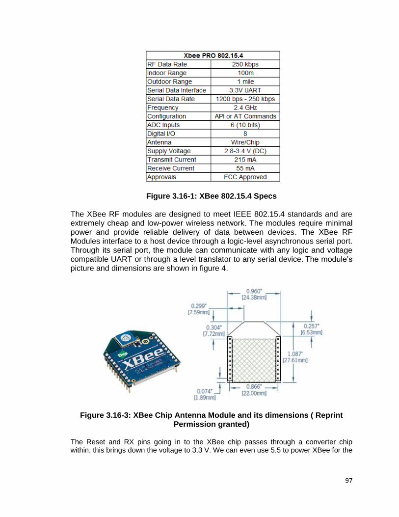
97
Figure 3.16-1: XBee 802.15.4 Specs
The XBee RF modules are designed to meet IEEE 802.15.4 standards and are extremely cheap and low-power wireless network. The modules require minimal power and provide reliable delivery of data between devices. The XBee RF Modules interface to a host device through a logic-level asynchronous serial port. Through its serial port, the module can communicate with any logic and voltage compatible UART or through a level translator to any serial device. The module‟s picture and dimensions are shown in figure 4.
Figure 3.16-3: XBee Chip Antenna Module and its dimensions ( Reprint Permission granted)
The Reset and RX pins going in to the XBee chip passes through a converter chip within, this brings down the voltage to 3.3 V. We can even use 5.5 to power XBee for the

98
communication. XBee connected to the adapter with its pin out reference is shown in figure 5.
Figure 3.16-4: XBee’s reference pin out
Once we have this connection done, we simply plug in the FTDI cable into the XBee adapter to the relative pins and the other end will go into the computer. Now it is time to setup the software for it. We are planning to work in Microsoft Windows so far to provide the easy accessibility. To configure the receiver, all we have to do is go under the Control Panel and look for Device Manager, under Device Manager we will need to look for “USB Serial Port” to figure out the COM port used for the USB. The program used is called X-CTU which helps to configure and upgrade the firmware. X-CTU can be downloaded from a couple of websites which are devoted for XBee‟s users. After downloading and installing the program we will have to select the COM port and baud rate which is 9600 by default. Flow Control should be set as “None”, Data Bits should be set as “8” and Stop Bits should be set as “1”. After setting up the X-CTU, the program should like figure 6 [33].

99
Figure 3.16-5: X-CTU
To verify if everything is done so far is correct, click in the “Test/Query” tab and if all the work so far is successful, we should see a message similar to figure 7.
Figure 3.16-6: Verification Dialog Box
If for some reason we don‟t see the message above, we will have to check if the XBee is powered correctly which can simply be checked by looking at the green LED on the XBee adapter. It is always a good idea to give the X-CTU program a second look to make sure everything is set properly.

100
Along with the receiver XBee chip, we will check the transmitter XBee chip to make sure it is working fine as well which will provide us not to troubleshoot the transmitter chip in the future. This step verifies that the communication of XBee chips with the computer is successful. As discussed earlier, it is necessary to update the firmware which leads to our next step which is configuring and updating of the chips.
3.16.2 CONFIGURE: So far, we have developed the receiver for the base station and connected it to the computer using the FTDI cable. If the XBee respond to the X-CTU program and the LEDs are blinking, we will proceed to configure the firmware. First we will open the X-CTU program and go to the Modem Configuration tab; this is where the built modem is configured and updated. On the same dialog box there is an option to download the new version of the firmware using the web, for that we have to make sure that our computer is connected to the internet. Once the downloading is done, we will upgrade the modem but first we need to check the current version and settings which can be read under Modem Parameters. We need to know exactly what version and setting are stored in the modem. From the “Version” drop down menu, pick the latest version and then click on “Write” to update the modem to the latest version. It is recommended to update the transmitter and receiver chip together and label them so we will know in future both chips are updated and ready to go. Both the transmitter and receiver chips need to be updated but we will only need to configure the transmitter chip. The reason behind configuring the transmitter chip is to allocate the XBee pins to read certain data from the microcontroller. The configure process also help to set up the chip‟s speed and size of the data transmission. In order to configure we will have to know the specs of the microcontroller and some more details which will be done in senior design II. If there are more XBee networks are present in the area, which is possible, we will have to change the PAN ID to a different number. PAN ID is a four digit HEX number and we will have to make sure the one we choose is different than the other networks. A unique PAN ID number for each module keeps multiple XBees network to function properly without interference. We will need to save the configuration to XBee‟s permanent storage once they are upgraded and set with a unique PAN ID.We can also configure the modules using AT commands [33].
3.16.3 TRANSMITTER: Transmitter will be the XBee module which is connected on the printed circuit board next to microcontroller. For transmitter we are using the same 802.15.4 XBee module which will be used for the receiver. A generic connection of XBee module is shown in figure 8.

101
Figure 3.16-7: Microcontroller and XBee data transmission
The XBee module will be connected to the UART port on the PIC. In order to communicate between microcontroller and XBee chip, schematics shown in figure 9 should be used.
Figure 3.16-8: PIC to XBee connection (No permission required)
To interface the setup in figure 10 is required. Figure 10 shows the schematics for the circuit. We will connect the XBee to the PIC18LF24J50 through a UART
interface. In order to use the TX and RX pins on the microcontroller, Port C must be open so that we can use these pins for USART (Universal Synchronous Asynchronous Receiving and Transmitting). The PIC18LF24J50 is capable of both synchronous and asynchronous operation but must be configured for asynchronous signal for the Xbee module. For successful serial communication, the UART‟s must be configured with the same baud rate, parity, start bits, stop bits, and data bits. On the microcontroller, pin 25 is for transmission and pin 26 is for receiving. We will add a voltage divider circuit to support the input voltage range of the UART serial signal to pin 2 and pin 3 on the Xbee chip [33].

102
Figure 3.16-9: PIC to XBee Circuit Schematic To synchronize the microcontroller to with the XBee firmware which is known as X-CTU we will have to run a few codes in C programming language which are discussed below. Transmitter Code With this code the transmitter checks the pin AO to see if it is high or low. If the pin is high the transmitter sends the signal “a” to the receiver and turns the LED on. If the signal is low, the transmitter sends the signal “b” to the receiver [34]. #include <18f4520.h>
#fuses HS,NOLVP,NOWDT,NOPROTECT
#use delay(clock=20000000) // 20 MHz crystal on PCB
//#use rs232(baud=19200, xmit=PIN_A0, rcv=PIN_A1)// use any pins for
UART
#use rs232(baud=9600, UART1) // hardware UART good; uses RC6/TX and
RC7/RX
// characters transmitted faster than the capability of PIC to handle
them will hang the UART
#include <stdlib.h>
#define LED_0 PIN_D0
void main()
while (TRUE)
if (input(PIN_A0))
output_high(LED_0);

103
printf("a"); //sends signal a
else
output_low(LED_0);
printf("b"); //sends signal b
Receiver Code The receiver checks the signal from the XBee and if the signal is “a”, the receiver turns on the LED.
#include <18f4520.h>
#fuses HS,NOLVP,NOWDT,NOPROTECT
#use delay(clock=20000000) // 20 MHz crystal on PCB
//#use rs232(baud=19200, xmit=PIN_A0, rcv=PIN_A1) // you can use any
pins for software uart...
#use rs232(baud=9600, UART1) // hardware UART good; uses RC6/TX and
RC7/RX
// characters transmitted faster than the capability of PIC to handle
them will hang the UART
#define LED_0 PIN_D0
#include <stdlib.h>
char x;
void main()
while (TRUE)
if (kbhit())
x = getc();
if (x=='a')
output_high(LED_0);
else
output_low(LED_0);
3.16.7 ADDRESSING: Every RF data packet sent over-the-air contains a Source Address and Destination Address field in its header. The RF module supports both 16-bit and 64-bit addresses. A unique 64-bit IEEE source address is assigned at the time of manufacturing. Short addressing must be configured manually. A module will use

104
its unique 64-bit address as its Source Address if it‟s MY (16-bit Source Address) value is “0xFFFF” or “0xFFFE”. To send a packet to a specific module using 64-bit addressing: Set Destination Address (DL + DH) to match the Source Address (SL + SH) of the intended destination module. To send a packet to a specific module using 16-bit addressing: Set DL (Destination Address Low) parameter to equal the MY parameter and set the DH (Destination Address High) parameter to „0‟ [35]. From the manufacturers, XBee is set to operate in Unicast Mode. It is the only case where the retries are supported. In Unicast Mode, the receiver sends an acknowledgment signal to the transmitter, and if the transmitter does not receive the acknowledgment signal, the transmitter sends the data up to three times and if it fails all three times then an acknowledgment failure is recorded.The module can be configured to use short 16-bit addresses as the Source Address or the Destination Address. The module can also be configured to use long 64-bit addresses as the Source Address or the Destination Address. Then there is a Broadcast Mode where the module will accept the message containing a broadcast address but there will be no re-tries. Neither the receiver sends back an acknowledgment message nor does the transmitter try to resend the data.
3.16.8 XBEE’S MODES OF OPERATION: XBee operates in five different modes which are listed as follows:
Transmit Mode Sleep Mode Idle Mode Receive Mode Command Mode
The XBee is said to be in Transmit Mode if the serial data is received in the DI Buffer as shown in figure 11. XBee is in Sleep Mode if one of the specific sleep conditions is met. Sleep Mode enables the module to enter low-power consumption when not in use. Idle mode is simply the state where the module is not receiving or transmitting any data. XBee is operates under Receive Mode when a valid RF data is received through the antenna of the chip and finally it is under Command Mode if the command mode sequence is issued. When the data is transmitted, it holds a Source and Destination Address field. The source matches the destination and that‟s how the data is transmitted to the right location. There are two ways in which data is transmitter, direct and indirect transmission. In direct transmission data is transmitted right away to the destination. Indirect transmission, the data is transmitted upon request. For example the destination module has to request for the data to be transmitted. [36]

105
Above discussion completes the hardware part of the project and now it is time to move on the software part.
3.16.9 BASE STATION SOFTWARE: We all know that hardware is incomplete without software. Now it‟s time to discuss the exciting part which is the software. The software lets us saves the data to the computer or upload to a database for data monitoring. The software that communicates with XBee is written in Python. So we are also leaning towards using Python. Python is really fast to develop and has multi operating systems. On the negative or positive side, depends how we see it, it is very popular among software and hardware hackers. The XBees communicate through the serial port so we can use any programming language for example, C, Java etc. Using Python is not a requirement, but it just makes life easier and it is really easy to learn as well. Another option is to use the “EnergyLogger” which is a program that is available for and can be downloaded online. It is free for residential usage but there is some licensing fee involved for commercial usage. Energy Logger is design to log real time data and energy usage. The data files created by EnergyLogger can be merged with the “EnergyProbe” which is also a free application used for research and energy usage analysis. Energy Probe is wirelessly record data and interprets energy usage. The user interfaces for Energy Logger is shown in figure 12 [37].
Figure 3.16-10: Energy Logger User Interface

106
CHAPTER 4: TESTING: In order to produce a product in the market, there is always a testing procedure. In summary, testing of device is conducted to ensure that the device will serve the intended purpose not just at ideal conditions, but in all sort of conditions. The conditions could be the difference of temperature, climate, time of the day etc. Since our project is critical to atmospheric conditions, it is mandatory to run thorough testing on it, not just before it is built, but also after it is built to make sure we are getting the desired results. Although it is not possible to achieve ideal results, we will try to get results that are next to ideal. Our project is a prototype for future UCF solar farm, it is very important for us to make it as efficient as possible so we can provide UCF with the best product and in turn, UCF will get the most energy out of the solar farm. For that purpose, we will be testing our prototype in extreme atmospheric conditions. We have decided to run multiple tests to figure out how the efficiency of the module varies with different cases. The first test is to make sure that there are no physical damages on the solar panels. Second, make sure that inverter and the microcontroller board are secured in a protective casing and all the wired connections are solid. In short, check the physical functionality of all the parts being used. Once the physicals are done, then we will run different tests and if the device performs and provides the relative results, that means our device is successful. We are just finishing our research phase and are at the beginning of development phase as required by the syllabus of senior design I, we cannot really run desired tests. So here we are going to talk about different testing that will take place in senior design II. Following is the discussion of different tests which will be conducted:
4.1 INVERTER TEST: The very first test will be the inverter test. Since inverter is pretty much the back bone of the system, we want to make sure it is up and running properly. The inverter is intended to go in to the grid, but we will not really know if we just let it go to the grid. Thanks to Fronius IG 3000 inverter, it provides charge controller and an AC power outlet so we can hook up any load. After connecting the solar panels in series, we will run the wires straight to the inverter without using any of the sensors. For the test, let‟s say if the panels are supposed to produce 2500 W and 320 V max, we should see at least 2200 W of power generation taking in account the efficiency of solar panels and the inverter. Now we will hook up a load, like a laptop computer, if it powers the laptop, then we know the inverter is in perfect shape and has passed the test.

107
4.2 MICROCONTROLLER AND PCB TEST: This test will be the most critical test and will require the most amount of time. All the other components of the system are basically plug and test, but this one requires a great deal of perfection and durability. We have already put an order for the microcontroller development kit and sensors. Once we receive the order, we are planning to run tests on each sensor to make sure all the sensors communicate with the microcontroller without any problems. We will just hook up a DC source like a 12 V battery and run the diagnostics test. For example, we have to check if our voltage is scaled down to 5 V properly through voltage divider circuit and then if that 5 V is converting from analog to digital through microcontroller A/D pin. Next we will check all the current and temperature sensors by connecting them on the development board to make sure all of them work fine. PCB problems are very common because a third party is involved (PCB vendor). For example, the components on the circuit board or the board itself could be defected. Therefore, once the PCB is acquired from the vendor, we will have to be very careful to solder the resistors, transistors, sensors and any other necessary devices onto the circuit board. But even if this extra measure is taken to make everything is done correctly there could be some faults in the circuit board. Here are some of the typical problems that might cause the board to not work properly:
Faulty solder joints
Oscillation/Distortion
Incorrect terminal connections
Incorrect components
Design errors
Schematic errors
Defected PCB First step of the test should be the examining of the circuit board for any sign of cracks, discoloration, or burn mark, corrosion, and unintentional soldering that might cause a short circuit. If none of the problem can be visibly indentified, then an oscilloscope and a multi-meter will be used to trace all the resistors and sensors to verify that they are inputting and outputting the correct voltage and signal. The continuity function on the multi-meter can be use to determine if the soldering is well connected between the PCB trace and the components pins. It can also be used to detect whether the PCB tracing or a wire is broken even if they can‟t be seen with naked eye. Once a defected component is identified, it will be replaced with a new one.

108
Test Procedure: The chosen microcontroller PIC18LF24J50 will need to be tested not just for proper functioning but also for the coding. The form factor of the microcontroller will not allow the testing to be easily done if we decide to use a breadboard available in the senior design lab. We may have to connect the microcontroller using a special connector so it is programmable using the breadboard. Since the microcontroller is really cheap, we will not hesitate to solder it to a DIP adapter for testing. This will let us conduct the tests on a breadboard without a PCB. After soldering the microcontroller to a DIP adapter, we will connect it on a breadboard along with the resistors, inductors, op-amps and other necessary components. Figure 1 shows an example for a 44-pin TQFP to DIP connector, which will be used for testing purposes.
Figure 4.2-1: TQFP to DIP adapter Reprinted with Permission Pending From
Once we place the microcontroller on the breadboard using the DIP adapter, we will start the coding to test it to make sure it is interacting with other electrical components. We will use MPLAB IDE which is a simulator for PIC processors to write and test the code. Doing so will also help us in debugging the code since it has default debugging capabilities. It will allow us to simulate the program that is created for microcontroller without programming the microcontroller itself. This procedure will provide us the sense of satisfaction as it will be doing all the work virtually. Besides, it is available for free and can be easily downloaded from the Microchip website.
The next important testing is of the data transmission. Data coming from the sensors will be encoded and transmitted using UART. To read the transmitted

109
data, we will have to install a data logger on a computer such as Hyper Terminal. Hyper Terminal will watch and interpret incoming data while the power is on for the breadboard. The data acquired will be compared to the data obtained from the oscilloscope to see the accuracy.
4.3 COMPONENT TESTING: For component testing, we will have to connect the breadboard along with the sensors, microcontroller and the rest of the electronic components to a computer using a DB9 connector. Sensors will be connected to the analog input pins of the microcontroller. A typical DB9 connection is shown in figure 2. The TX pin of the microcontroller is designated for DB9 connection and eventually it will be connected to a computer. We might have to install a voltage controller to keep the voltage difference between the microcontroller and the DB9 to a minimal amount. The UART part of the microcontroller will interface between the microcontroller and DB9 in a setup shown in figure 2. UART is used basically to make sure that the data is sent serially to the computer and once the data starts transmitting; Hyper Terminal will take care of the rest. HyperTerminal will display the data acquired from the current, voltage and temperature sensors in a user friendly easy to read manner.
Figure 4.3-1: DB9 connection

110
4.4 WIRELESS CONNECTIVITY
TROUBLESHOOT: We have decided to use WiFi wireless connection to take data from microcontroller and send it to the computer for display. We have to make sure that the wireless connection is solid at all times to avoid any interruption in receiving of the data. There are a few different reasons for not getting a good connectivity which are discussed below: Problem due to power: This problem can be resolved by making the access point as accessible as possible by removing the objects nearby. Load-bearing walls or concrete slabs greatly make the signals weak greatly. If it is a MIMO access point, we can change the orientation of the antenna. Interference of other wireless networks: Wireless networks side by side creating disturbances. Since we will have a lot of wireless network activity besides our connection, we will need to change the broadcast channel default access point to minimize interference. We will also have to change the network name (SSID) by default. Inappropriate frequency: Some brands of WiFi receivers have preferences on the channel used by the WiFi access point. Therefore some of them even when they are only 4-5 yards away from the modem will have an unstable connection. We will test several channels to see which one has the best connectivity. General receivers tend to work better on higher channels. Interference due to a DECT cordless phone: DECT cordless phones use the same frequency band as WiFi which is around 2.4 GHz. In fact microwave ovens also have the same frequency radiation. We will have to make sure that there is no DECT base around the modem and there are no microwave ovens situated at least 4-5 yards from the modem. USB extension cable: WiFi dongles provide an extension cord to connect the USB key. This extension may create some interference, so we will not be using any extensions. Network protocol unstable: Some network protocols are relatively unstable in a WiFi connection and can cause loss of connections. We can just uninstall the protocol form our computer. Wireless camera interference: Wireless cameras use frequencies of 2.4Ghz, so just like DECT phones; we need to make sure there are no wireless cameras installed nearby modem.

111
4.5 WATER RESISTIVITY: Our prototype will be installed at the open field and all the connections are going to take place at the field as well. So it is very crucial to keep it water proof. Although we picked water proof panels and inverter, that‟s just a part of securing the system from water. We still have to make sure all the wires are waterproof and the circuit board is out of reach of water. The mechanical engineering team is responsible for the mounting system and they are making a special inlet for wires to pass through without getting affected with water. Even though wires will have insulation, we don‟t want to take any chances of components shorting out due to contact with the water. Short circuit is really undesirable as it can cause the sensitive element to blow up or catch fire and we don‟t want that to happen as it will make us purchase and install the components over again. Figure 1 shows the waterproof setup of our system. All the secondary microcontrollers are secured in a protective casing. The primary microcontroller is placed next to the inverter in the same protective casing. The primary microcontroller and inverter are also covered by another protective casing as shown. Once all the water proofing is done, we will run the water test which will mimic the water fall due to rain, hurricane or any other situation. This test will take place at the field, after successful installation of all the components. Solar panels will be under the shade of large cardboard which will serve the cloudy climate. A garden hose with a spray or shower setting will be used to continuously sprinkle water at a gentle pressure on the solar panels. This process will continue for 5 minutes. We will check the variations in the data before and after halfway through in the spraying process. We should see a decline in the power production and the numbers should decline significantly after 5 minutes. Now we stop the spraying process and let the solar panels dry and remove the cardboard and 10 minutes later, the numbers should go back to normal. If we observe the fluctuation in the data during this process that means our product has passed the water test successfully.

112
Figure 4.5-1
4.6 WIND AFFECT: Next we are going to run a test to check the effect of wind on the solar panels. The setup shown in figure 1 is capable of handling up to 130 mph of wind. The wind shouldn‟t affect the connectivity of wires and cannot cause destruction to any of the components. For the test, we have requested the UCF department of landscaping to let us borrow six leaf blowers. Each blower can derive the wind up to 100-150 mph depending upon the size and specs of it. Blowers will be directed towards the panels and with help of our fellow industrial engineers we can point six blowers at the panels easily and one of our EE will be monitoring the data on the computer to see any fluctuation. We are not really sure how wind affects the efficiency of solar panels so it might turn out to be a surprise. There is no data to be found using wind pressure on the panels online or on any of the texts. Even if wind hardly makes any changes in the efficiency of the solar panels, we will conduct this test to see what kind of results we acquire. We are hoping to see no changes in the efficiency of the power production. This test will be a 100% success regardless of the outcome.

113
4.7 TEMPERATURE TESTING: All the components are capable of working in a quite large range of temperature from cold to hot. There is no need to take extra measurement to protect the components especially in Florida where climate not harsh. Since all the assembly is going to be done outdoors at a fixed point and the whole system is almost 35 feet long, it is almost impossible to out the panels under different temperature conditions. However, we are will transition from winter to spring before the end of our project deadline, we will be able to check the data collection between two seasons. The cells of solar panels are dark in color and operate at much higher temperatures than the air temperature. The hotter these cells are, the higher the voltage drop is. This is why it is important to use panels that have a little bit of higher operating voltage than the required load voltage. For the test, we will pick best five days during winter season when the temperature is optimal and best five days during spring season with optimal conditions and record the data. This test will take the largest amount of time as we will have to wait for the change of the season. After we have the collection of data from both seasons, we will compare the data and if we see the variation in the data that means our product has passed the temperature test successfully. We are hoping to see better results in the winter time because the solar panels will not heat up during the daytime. High temperature is famous for degrading the efficiency of the solar panels.
4.8 CLOUDS AND SHADE AFFECT: UCF has allocated an empty plain field for the solar farm project. Since the panels will be connected in series, if one of the panels is under the shade of a tree, all the panels will be affected. We don‟t have to worry about trees blocking the sunlight but on the other hand, clouds blocking the sunlight cannot be resolved. As soon as the clouds go over the sun, the level of energy you we get decreases. But it doesn‟t mean we don‟t get light on the panels. Panels continue to absorb the refracted sunlight. In a normal cloudy day, not when there are enough clouds to not cast shadows, we should still get fifty percent of the maximum capacity without clouds. The thicker the coverage of clouds, the smaller the amount of electricity we get. For the test, we will pick three different days. First with clear sky, which will be our reference point, second day will be a lighter density of clouds and the third will be the thickest density of clouds sometime before a rain storm. If we get at least half of the power production on the second day and some amount of power

114
production on the third day as compared to our reference point, this test is successful.
4.9 DUST AND DIRT TEST: Dust and dirt seem to affect the efficiency of solar panels. Dust and dirt act as a potential barrier between sunlight and the panels. Solar panels exposed to more dusty area like desert are more likely to lose power and require regular cleanings. Solar panels can lose up to 10% power with only a small amount of dust which is a major loss. We will characterize the effect of dust on solar panel performance. To achieve this goal, we will try to determine the rate that dust deposits on solar panel glass and how much sunlight is absorbed and reflected by dust. The ultimate goal is to understand how important it is to keep solar panels clean and exactly harmful it is to not keep the panels clean. For the test we will cover the panels with talcum powder or regular sand. After the dust sitting on the panels for about 10 minutes, we will check the readings and see how the efficiency is affected. We are expecting to see a decrease in efficiency. If we see a decrease of at least 3%, the device is successful.
4. 10 HUMIDITY TEST: We haven‟t really found any data regarding humidity side-effects on the efficiency of microcontrollers or panels. Since the microcontroller will be sealed in protective casing we assume that humidity will not affect microcontroller. And condensation on panels will normally be at night time, it is safe to assume that there will not be any affect on the efficiency of solar panels as well. So we have decided not to worry about the level of atmospheric humidity and not to conduct any tests regarding humidity.
CHAPTER 5: PREVIOUS WORKS:
5.1 SOLAR SYSTEM/MONITORING SYSTEM: In the beginning of the research for this project the group members decide to look in past similar and related projects to study their designs and approaches to solve the problems at hand. We were able to find similar projects done by UCF students where they designed and successfully implemented a monitoring system for an array of solar panels.
5.1.1 SOLAR PANEL MONITOR SYSTEM:

115
The Solar Panel Monitor System group had the task of designing a monitoring system that is able to monitor the power output of six solar panel strings, and to send the data wirelessly to display the results to the user and alert them if any of the strings is not functioning properly. This is very similar to the task we have the difference is that we are attempting to monitor the panels individually. In their project they used a PIC24 to handle the data sent by the current and the voltage sensors, the data received is converted from analog signals into digital and then transmits the data wirelessly using a ZeroG module. They employed the energy produced by the solar array to provide the power necessary to operate the microcontroller and the sensors. To measure the voltage they employed a step down circuit to get the voltage in manageable range. They used a voltage dividing circuit in conjunction with a shunt resistor to detect the voltage drop across a resistor in the circuit with a known resistance. To measure the current produced by the array they used a Hall Effect current sensor. The next step after the collection of the data by the microcontroller is to transmit back to the base station (a wireless access point with custom firmware) where they choose to use DD-WRT as the firm ware of the device because of it is broad device support and large open community support and its free availability for small application devices. As for the hardware of this device they built their choice on a device being able to store the data it received in an external USB storage and its ability to have an external antenna able of transmitting and receiving data for long distances. As a development tool for their microcontroller they employed the Explore 16 board. They made the decision to use this board as a result of:
Allows independent I/O mapping of many peripherals
Continuous hardware integrity checking and safety
Provides clock, calendar and alarm functions
Programmable Cyclic Redundancy Check (CRC)
Two 3-Wire/4-Wire SPI modules
7-Bit/10-Bit Addressing
On-chip hardware encoder/decoder
Wide operating temperature range of -25° to +70°C
This project was sponsored by QuickBeam Energy and Progress Energy.
5.1.2 SOLAR ARRAY MONITOR: This project had the same task to be accomplished by the first one but took a slightly different approach in engineering the components in achieving the same result. This shows us that each team of engineers will employ a different approach to solve the same problem.

116
In their design they choose the PIC18F4458 for its twelve AD converters with twelve bits of precision, FLASH program memory, and internal clock, out of these twelve convertors they used two for each string one taking in a measurement of the current sensor and the second for the voltage reading which will require 10 of the ad convertors then they used one of the remaining pins to measure the temperature of the system. The internal clock is utilized in keeping track of the time of each reading taken by the system. The collected data was then sent by a serial communicating module. They choose to power the components using a separate solar panel which made design in the power supply system easier since it eliminated the need of stepping down the high and highly varying voltage. For this task they choose a solar panel capable of producing 15 watts at a maximum current of 1 amp, then used a simple regulating circuit to get the 5V 300 mA required by t he system. for the current sensor they used the CSA-1V which is a single axis Hall effect sensor which uses the magnetic field produced by the current in the wire and produces a voltage proportional to the value, knowing how far is the wire‟s center located from the chip it is possible to calculate the current according to the formula; Vout=0.060×I/(d+0.3mm), this chip provides the reading in two forms the first is a single ended result varying between 0V – 5V and then there is the differential output used by the design team which produces a voltage between 0/+- 2.5V with respect to an internal reference. For the temperature reading they used the LM34DZ which is an analog sensor that has a linear output 10mV per degree Fahrenheit. This sensor can measure a temperature between −40° to +230°F and has an accuracy of ±1.0°F (at +77°F). For the voltage sensing circuit the main concern they had was the high voltage produced by the solar array, they had to consider different resistances as to limit the amount of power drawn by the resistor and to limit the potential damage to the system. For communicating the data back to the user they used WIZ110SR. The WIZ110SR is a protocol converter that transmits data sent by serial equipment to Ethernet. The input received by the serial port on the WIZ110SR is sent to a W5100 by MCU. The device will operate in client mode and will initiate a connection to the Quick Beam Energy servers at intervals of 15 minutes. They used the static IP address of the device and the IP address of the Quick Beam Energy servers will be static or acquired through a DNS query. Their readings are transmitted every 15 minutes when the sampled data is complete.
CHAPTER 6: PROJECT BUDGET:
6.1 BUDGET PROJECTION: The idea for this project was proposed to the senior design one class was Mr. David Norvel of the facilities and maintenance department at UCF. One of the stipulations of the proposed project was that the project would be completely funded through his department. The proposed total budget amount for the project was initially ten thousand dollars but as more departments from the college of

117
engineering came on board and the complexity of the project changed the total project budget was increased to twenty thousand dollars. Below Table 6.1-1 is a list of the estimated cost to produce and purchase each part of the solar fields design.
Parts List
Part Part Number Cost
240 Watt Solar Panel NU-U240F $612.00
Wire Wound Resistor (5k)
PPC3W5.0KCT-ND $1.10
Wire Wound Resistor (5k)
PYR7511-27 $4.48
5.1V Zener Diode PPC3W5.0KCT-ND $0.27
Operational Amplifier LM393NFS-ND $0.40
Current Sensor CSLT6B100 $9.36
Temperature Sensor SA1-RTD $50.00
RJ45 Crimp Tool RJ45CR $14.99
RJ45 Cable NET1 $1.15/ft or $1.00/10ft
RJ45 Female Connectors
WM3245-ND $1.41
RJ45 Male Connectors Walmart Set of 25- $5.00
Terminal Block Eurostyle Terminal Block
796740 $1.22
Multiplexer MPC506A $11.92
Microcontroller PIC18LF24J50-I/SS-ND $3.26
Wireless $250.00
Table 6.1-1: List of the Estimated Cost

118
6.2 TOTAL ARRAY COST: 12 Solar Panels = $2.55/Watt * 240 Watts * 12 Panels = $7,344.00 12-5k Wire Wound Resistors = 12 Resistors * $1.10 = $13.20 12-27k Wire Wound Resistors = 12 Resistors * $4.48 = $53.76 12-5.1V Zener Diodes = 12 Zeners Diodes * $0.27 = $3.24 12 Op-Amps = 12 Op-Amps * $0.40 = $4.80 12 Current Sensor = 12 Current Sensor * $9.36 = $112.32 12 Temperature Sensors = 12 Temperature Sensors * $600.00 1 RJ45 Crimp Tool = $14.99 100 Feet RJ45 Cable = $10.00 24 RJ45 Female Connectors = 24 RJ45 Female Connectors * $1.41 = $33.84 24 RJ45 Male Connectors = $5.00 (Walmart) 30 Terminal Blocks = 30 Terminal Blocks * $1.22 = $36.60 3 Multiplexers = 3 Multiplexers * $11.42 = $34.26 1 Microcontroller = 1 Microcontroller * $3.26 = $3.26 1 Wireless = $250.00 12 Secondary Printed Circuit Boards = ~$75.00/Board 1 Primary Printed Circuit Board = ~$100.00 Total Cost = $9594.27 Total Cost Monitoring System = $2250.00

119
6.3 ASSESSMENT: If total monitoring of the entire system is desired it comes with a high price tag. When the three megawatt solar field is installed there will be monitoring of the entire field but it will be done array by array instead of panel by panel. For this system we have set up a monitoring system for twelve individual panels but in the overall design will monitor twelve different solar panel arrays. Of course the design at the point will have to be redone because the total power output of an array of twelve solar panels is going to much greater than that of a single panel. There are a few things that can be done here though to reduce to the price of the proposed monitoring system. For one, the temperature sensors, besides the solar panels, are the single most expensive electrical component that needs to be purchased. So, maybe instead of monitoring the temperature on all twelve of the panels, the temperature can simply be measured on two or three panels and an average calculation can be done during the processing of the data by the system. Another option would be to maybe design a homemade thermocouple device out of cheaper parts. The problem with that is the life expectancy of the part could be severely shorter than that of the purchased thermocouple. All of the electrical components that were selected were through hole parts. This was done on purpose because in the event of a part malfunctioning we as designers need to be able to remove the faulty part and replace it with a properly working part. If, when we make the prototype board, the assembly of the board is manageable the cost of having an outside printed circuit board company produce the thirteen boards can be removed from the overall cost. For the sake of time and simplicity though having an outside company produce the boards may be an unavoidable cost of the project. The only other place that money can be saved is in the parts themselves. A lot of research went into the selection of the parts so we are not sure how much money can be saved on the parts without sacrificing quality. There are some alternate options for moving the data from the primary circuit board to the web where the data is going to be collected and those options will be examined further in the coming weeks.
CHAPTER 7: CONCLUSION
7.1CONCLUSION: To complete this project in an effective manner a thorough understanding of solar technology and important aspects of it is essential. A variety of different applications were researched and determined whether or not they are even feasible at the current state of solar technology. The popular application for solar

120
power used to be for remote locations requiring small quantities of power to run lighting, pumps, and other low power applications. But now with technology advancement, solar panels efficiency has gone much higher. The new trend is to build huge solar farms and get as much energy possible, which defines our project. The steps involved in this project turned out to be very critical and complicated since our project is a relatively larger than normal senior design projects besides the fact that our sponsor is very strict about the requirements and outcome of the project. After an intensive research, our team has done a terrific job of finding the best and most efficient parts for the project. Overall we have a very good understanding of the project and we have familiarized ourselves with all the parts which will be used in development of the project in senior design II. All the necessary schematics along with the circuit diagram have been done as well. Our sponsor, UCF Department of Energy, is satisfied with our progress so far. Through the intensive research, we have learned a lot about the latest and greatest technological ways conserve the energy better than before. Our project consists of three major parts, a solar array, microcontroller and a base station. The idea is to capture the solar energy and convert it into AC voltage so we can take advantage of natural resources. And to create the awareness, we will be monitoring and displaying the power production by the solar panels and comparing to conventional energy production. The comparison will create the awareness when people can see how much money they could be saving due to solar panels along with helping the world to go greener. Solar Farms is the new fashion. Power companies and residential homes have become increasingly more interested in installing photovoltaic arrays as a way to become more carbon neutral or “Green”. Over the course of this project a number of practical problems were encountered that a typical engineer would run into. Working with and for two different advisors that helped us solve these types of problems provided us with a solid basis for what to expect in a business environment. This form of project gave us a unique for of experience that would not be available in a typical classroom.

121
BIBLIOGRAPHY: [1]. http://eosweb.larc.nasa.gov/cgi-bin/sse/sse.cgi
[2]. http://www.livestrong.com/article/212570-advantages-of-a-monocrystalline-solar-panel/ [3]. http://www.iea-pvps.org/pv/materials.htm [4]. http://www.solarpowerfast.com/build-solar-panel/thin-film-solar-panels/ [5]. http://www.solarfeeds.com/ggs/6259-advantages-of-thin-film-solar-panels [6]. http://ezinearticles.com/?Advantages-and-Disadvantages-of-Solar-Film-Cells&id=1961400 [7]. http://www-03.ibm.com/press/us/en/pressrelease/29404.wss [8].http://en.wikipedia.org/wiki/Organic_solar_cell#Types_of_junctions_for_OPVC [9]. http://en.wikipedia.org/wiki/Solar_energy [10]. http://www.windows2universe.org/earth/climate/sun_radiation_at_earth.html [11]. http://www.solarpower2day.net/solar-cells/efficiency/ [12]. http://sunelec.com/index.php?mainpage=index&cPath=1 [13]. http://www.countrymilewifi.com/what_is_wifi.html [14]. http://en.wikipedia.org/wiki/Bluetooth [15]. http://en.wikipedia.org/wiki/ZigBee [16]. http://www.awarepoint.com/documents/AtoZigbee-s.pdf [17]. http://robosavvy.com/store/product_info.php/products_id/426 [18]. http://en.kioskea.net/contents/cpl/cpl-intro.php3 [19]. http://support.radioshack.com/support_tutorials/batteries/batgd-b.htm [20].Google books, Rechargeable Batteries Applications Handbook. [21].http://wordiq.com [22]. http://www.mpoweruk.com/nimh.htm [23]. Lithium Ion Rechargeable Batteries: Materials, Technology, and new Applications. By Kazunori Ozawa. [24]. http://ezinearticles.com/?Advantages-and-Disadvantages-of-Solar-Tracking-Systems&id=2362743 [25]. http://www.helmholz.us/smallpowersystems/Intro.pdf [26]. http://www.tpub.com/content/firetrucksandequipment/TM-9-254/css/TM-9-254_217.htm [27]. http://en.wikipedia.org/wiki/Resistor [28]. http://www.onsemi.com/pub_link/Collateral/1N5333B-D.PDF [29]. http://www.nullmodem.com/RJ-45.htm [30]. http://focus.ti.com/lit/ds/symlink/mpc506.pdf [31]. http://www.microchipdirect.com/productsearch.aspx?Keywords=DV164136 [32]. http://www.scientificcomputing.com/article-hpc-Numerical-Precision-How-Much-is- Enough-063009.aspx [33]. http://www.ladyada.net/ [34].http://hades.mech.northwestern.edu/index.php/XBee_radio_communication_between_PICs [35].http://ftp1.digi.com/support/documentation/manual_xb_oemrfmodules_802.15.4.pdf

122
[36].http://ftp1.digi.com/support/documentation/manual_xb_oemrfmodules_802.15.4.pdf [37]. http://www.miloslick.com/EnergyLogger.html
APENDIES: PERMISSIONS
PERMISSIONS RECEIVED: Hi Michael, You can use them as you please. See http://en.wikipedia.org/wiki/Theory_of_solar_cell for higher-quality versions. John ---- [email protected] schreef: > Name: Michael Gannon > > Email: [email protected] > > Message: Hello my name is Michael Gannon and I am a undergraduate in electrical engineering at the University of Central Florida. My team is designing a solar array for our senior design project and wanted to ask permission to use your images of your voltage and current to temperature chart for solar cells in our senior design paper. > > Thank you very much in advance. > > Sincerely, > Michael Gannon
Hi Michael,
Thanks for your recent request to use the information on our website -- permission
granted - but I would appreciate it if you include a url link to the page(s) you got the
information from -- as we our information is dynamic and we frequently update it and
add more linking articles as our published knowledge base continues to expand.
I'm glad to hear that such programs exist as there certainly is a growing need for
knowledgeable, well-trained people in the solar industry.
Good luck with your solar project. Will you actually build an array - or just design it?
Best regards,
Stevan von Fechtmann

123
Comments
To Whom It May Concern, My name is Michael and I am part of an
Electrical Engineering Senior Design group at the University of Central
Florida in Orlando, Florida. As an ABET accredited university, we are
required to design a project that encapsulates our entire undergraduate
education. We are designing a solar panel array for our school. We would
like to request your permission to reuse information (such as images and
text) from your website in our initial design documentation. Thank you
very much in advance. Sincerely, Michael Gannon
On 11/28/2010 7:03 PM, [email protected] wrote:
> GENERAL INFORMATION - MIDNITE
>
> NAME - Ahmad Buleybel
> COMPANY -
>
> Location - orlando, fl - United States
>
> MESSAGE - Hello,
> I\'m a senior electrical engineering student at the
University of
> Central Florida.
> I am currently designing a solar array and wanted to use
some
> pictures of your products that we are going to use in our
> project,could i be allowed to use pictures and information
from your
> website in my document.
> Thank you for your time,
> Ahmad Buleybel
>
> FROM - [email protected]
Aloha Ahmad,
Please feel free to use any of the information from the web
site.
Thanks for checking!
Cheers,
Tom Carpenter
sure - just credit and link to us, thanks!
On Sun, Dec 5, 2010 at 6:39 PM, Ahmad Buleybel
<[email protected]> wrote:
> From: Ahmad Buleybel
> Email: [email protected]
>
> ------------------------------------------------------
>
> Hello,

124
>
> I am a senior electrical engineering student at the University of Central
> Florida.
> I am currently designing a solar array onitoring system and wanted to use
> some pictures of your products that we are going to use in our project,
> could I be allowed to use pictures and information from your website in my
> document.
>> Thank you for your time,
> Ahmad Buleybel
> Office Use Only:
> From: Ahmad Buleybel
> Email: [email protected]
> Login Name: Not logged in
> Login Email: Not logged in
> IP Address: 132.170.90.202 - 132.170.90.202
> Host Address: node202.seg90.ucf.edu
> Date and Time: Sun Dec 5 2010 18:39:33
Thank you for submitting a support request. Your email has been assigned
case 149523. Please expect to hear a response from us in the next few
business days. If this is a time sensitive matter, please call us at:
877-878-4060
You may track the status of your request at:
http://support.altestore.com/support.cgi?do=track_call&id=149523&key=PLHBASJV
Thank you,
The altE Staff
altE Store
"Making Renewable Do-able" (tm)
http://www.altEstore.com/
Tel: 877.878.4060 or +1.978.562.5858
Fax: +1.978.562.5854
125
PREMISSION PENDING
1) Good Morning,
My name is Michael Peffers and I am a senior in the electrical engineering program at
the University of Central Florida. I am working on my senior design project and I have
come across some useful data for my project on your website. I would like to know if I
could have your permission to reprint this data in my final report. Below is the link for the
information that I have taken: http://floridatravelusa.com/wcharts.htm The data that I
need is the average temperature chart for the Orlando area. Full credit for illustration will
be given to you within the text of the report. Thank you and have a wonderful day.
--
Regards,
Michael Peffers
2) Good Day,
My name is Michael Peffers and I am an electrical engineering student at the University of Central
Florida. I am currently attempting to complete my senior design project and have found some
useful data on your website about wire wound resistors. I would like to know if i could have you
permission to reprint this data in my final documentation. All credit will be given to the source of
the data with in the report. The link for where I got the information form
is: http://www.ohmite.com/cgi-bin/showpage.cgi?product=axiohm. Thank you in advance for any
help that you can provide me!
--
Regards,

126
Michael Peffers
3) Good Day,
My name is Michael Peffers and I am an electrical engineering student at the University of Central
Florida. I am currently attempting to complete my senior design project and have found some
useful data on your website about wire wound resistors. I would like to know if i could have you
permission to reprint this data in my final documentation. All credit will be given to the source of
the data within the report. The link for where I got the information from
is:http://www.irctt.com/pdf_files/IBT.pdf. Thank you in advance for any help that you can provide
me!
--
Regards,
Michael Peffers
4) Good Day,
My name is Michael Peffers and I am an electrical engineering student at the University of Central
Florida. I am currently attempting to complete my senior design project and have found some
useful data on your website about the CSLT6B100 current sensor. I would like to know if i could
have your permission to reprint this data in my final documentation. All credit will be given to the
source of the data within the report. The link for where I got the information from
is:http://www.contractelectronica.ru/files/124/CSLT6B100.pdf Thank you in advance for any help
that you can provide me and my senior design team.
--
Regards,
Michael Peffers
5) Good Day,
My name is Michael Peffers and I am an electrical engineering student at the University of Central
Florida. I am currently attempting to complete my senior design project and have found some
useful data on your website about the Eurostyle Terminal Blocks796740. I would like to know if i
could have your permission to reprint this data in my final documentation. All credit will be given
to the source of the data within the report. The link for where I got the information from
is:http://search.digikey.com/scripts/DkSearch/dksus.dll?Detail&name=A98275-ND
--
Regards,
Michael Peffers
Hello my name is Michael Gannon and I am a undergraduate in electrical engineering at the University of Central Florida. My team is designing a solar array for our senior

127
design project and wanted to ask permission to use your image of tracking vs fixed efficiency throughout the day for a solar panel chart in our senior design paper. Thank you very much in advance. Sincerely, Michael Gannon Hello my name is Michael Gannon and I am a undergraduate in electrical engineering at the University of Central Florida. My team is designing a solar array for our senior design project and wanted to ask permission to use your images of solar radiation chart in our senior design paper. Thank you very much in advance. Sincerely, Michael Gannon