Direction Sensing RFID Reader for Mobile Robot Navigation-SiO

Progress In Electromagnetics Research, Vol. 130, 241–256, 2012
DESIGN AND FABRICATION OF WIDEBANDARCHIMEDEAN SPIRAL ANTENNA BASED ULTRA-LOW COST “GREEN” MODULES FOR RFID SENSINGAND WIRELESS APPLICATIONS
Y. Amin*, Q. Chen, L. R. Zheng, and H. Tenhunen
iPack VINN Excellence Center, Royal Institute of Technology (KTH),Stockholm, SE-16440, Sweden
Abstract—A parametric analysis is performed for a widebandArchimedean spiral antenna in recognition of an emerging conceptto integrate RFID along with several applications by using a singleantenna. The antenna is fabricated using state-of-the-art inkjetprinting technology on various commercially available paper substratesto provide the low-cost, flexible RF modules for the next generationof “green” electronics. The effects on electromagnetic characteristicsof the planar Archimedean spiral antenna, due to the use of paperare investigated besides other parameters. The proposed antenna isevaluated and optimized for operational range from 0.8–3.0GHz. Itexhibits exceptional coverage throughout numerous RFID ISM bandsso do for other wireless applications.
1. INTRODUCTION
RFID (Radio Frequency Identification) is considered an emergingleading technology in future telecommunications [1, 2], automaticidentification and data capture (AIDC) industries [3]. The RFIDmarket has grown in a two-dimensional trend one side constitutesstandalone RFID systems which are commonly found at present [4–6]. On the other hand, more ultramodern approach is paving its way,in which RFID needs to be integrated with broad operational array ofdistinct applications [7, 8] for performing different functions includingnavigation, broadcasting, and personal communication [9–11], tomention a few. Using different antennas to include all communication
Received 8 July 2012, Accepted 13 August 2012, Scheduled 14 August 2012* Corresponding author: Yasar Amin ([email protected]).

242 Amin et al.
bands is a straightforward approach, but at the same time, it leads toincreasing cost, weight, more surface area for installation, and aboveall electromagnetic compatibility issues [12]. Thus, there is the needfor wide-bandwidth antennas [13, 14]. The espousal of a single, small-sized wideband antenna is certainly more attractive because RFID isreplacing other identification methods by whistling about cost-effectivemore efficient solutions [15, 16].
Spirals are extensively used circularly polarized widebandantennas [17]. The wideband features of spiral antenna brought itto the limelight in recent literature, particularly for miniaturization.The fundamental inspiration for miniaturization is to slow down thewave traveling within the antenna structure. Numerous approacheshave been pursued to achieve it, which includes dielectric or magneto-dielectric loading, artificial materials, spiral arm shaping, distributedreactive loading and arm orienting vertically [12]. Conversely, whenusing the popular dielectric loading approach, the input impedance isalso lowered. On the other hand, when the wave velocity is reducedby meandering of metalized arms, the axial ratio also deteriorates [17].It has been established that coiling of the spiral arms provides forimpedance control [12, 18]. The vast majority of circuits fabricated onPCB use FR-4 [19–22]; thus this volumetric design or miniaturizationis weighty, whereas PET is commonly found in RFID inlays and tags.Furthermore, both FR-4, which is a ceramic-based material [23], andpolyethylene terepthalate (PET) are nonbiodegradable substances thatmay take decades to decompose in landfills largely contributing to thebulk of annually generated electronic waste.
This paper presents parametric analysis of a flexible, widebandArchimedean antenna, which is fabricated by utilizing an exceptionallyefficient and low-cost inkjet printing technique to print “green”conformal electronic circuits on paper substrate. Paper is extremelyeco-friendly requiring a few months to decompose organically inlandfills. Organic materials do tend to be more lossy at higherfrequencies, due to their affinity to water. However, by using thecorrect paper type and printing process, adequate radio frequencyperformance is achieved on paper-based RF circuit designs. Wedemonstrate the successful use of the proposed inkjet printedantenna for operational range from 0.8–3.0GHz. The design andsimulations are performed using ANSYS HFSSTM, whereas; themeasurements are performed in an anechoic chamber dedicated toantenna characterization. The proposed antenna successfully operatesthroughout the operational range of interest, thus expanding the scopeof simultaneously integrating several wireless modules while developingeco-friendly industrial solutions.
Progress In Electromagnetics Research, Vol. 130, 2012 243
2. “GREEN” ANTENNAS EVOLUTION
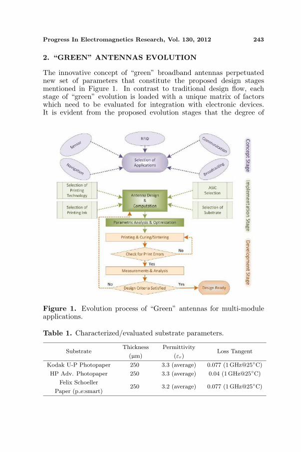
The innovative concept of “green” broadband antennas perpetuatednew set of parameters that constitute the proposed design stagesmentioned in Figure 1. In contrast to traditional design flow, eachstage of “green” evolution is loaded with a unique matrix of factorswhich need to be evaluated for integration with electronic devices.It is evident from the proposed evolution stages that the degree of
Figure 1. Evolution process of “Green” antennas for multi-moduleapplications.
Table 1. Characterized/evaluated substrate parameters.
SubstrateThickness
(µm)
Permittivity
(εr)Loss Tangent
Kodak U-P Photopaper 250 3.3 (average) 0.077 (1 GHz@25C)
HP Adv. Photopaper 250 3.3 (average) 0.04 (1 GHz@25C)
Felix Schoeller
Paper (p e:smart)250 3.2 (average) 0.077 (1GHz@25C)

244 Amin et al.
freedom at the concept level, limits the choices at the implementationphase than development. Therefore, much effort is devoted tothe implementation stage and design parameters are investigatedand optimized categorically. Two types of conductive inks, CCI-300 from Cabot Corp. and Nano-AG-120I from Xerox Corp. areevaluated by trial printing in combination with three different typesof commercially available paper substrates mentioned in Table 1. Thekey concept encapsulating the entire adaptation process is to achieverobust broadband antennas, which must show less sensitivity to theenvironmental variations that affect the paper dielectric constant.
3. SYNTHESIS OF THE ANTENNA TOPOLOGY
In order to achieve stable broadband multimode feature [24] multimodefeature in far and near fields planar Archimedean spiral antennastructure is realized. Three designs of a two-arm Archimedeanspiral antenna are assessed. The in-depth research proves that theArchimedean spiral is not a frequency-independent antenna structurebecause the spacing between the arms is specified by a constant, not anangle [25]. However, this is a contentious point because fundamentallyfrequency-independent performance is achieved over 10 : 1 bandwidths.The following numerical calculations are exploited to construct theproposed antenna structure in Figure 2. The centerline of the proposedArchimedean antenna is defined by:
r = aφ = r0 + (E)φ(1/S) (1)
where,
a =1K
dK
dC(2)
and C is the angle of rotation which depends on K. If the antenna isto be scaled to a frequency that is K times lower than the original
Figure 2. Dimensions & “green” theme of proposed antennas.

Progress In Electromagnetics Research, Vol. 130, 2012 245
frequency, the antenna’s physical surface must be made K timesgreater to maintain the same electrical dimensions [26]. The Expansioncoefficient (E) and the Spiral coefficient (S) of the proposed antennaare 1 whereas, r0 is the inner radius which is 1.6 cm. The pitch angleψ varies with radius as:
tanψ =r
a(3)
When r is large, then the pitch angle approaches 90. An equivalentdesign ratio τeq, which varies with radius, may be defined for theArchimedean spiral that has the same pitch angle ψ at radius r.Therefore,
τeq(r) = e−2π/| tan ψ| = e−2π|a/r| (4)
It is worth noting here that τeq approaches 1 for large value of r. Thesides of a strip may be defined in terms of the rotation angle φ ofFigure 2 and the angle δ (offset angle is 90 of the proposed structure)to get:
r = a
(φ± δ
2
)(5)
The radial width of the antenna strip Wr is a constant, which isindependent of radius and is obtained by:
Wr = aδ (6)
The actual width of the antenna strip varies to some extent with radiusand is calculated by:
W = aδ sinψ (7)
The spacing Sr between the centerlines of the adjacent turns for onearm is specified by:
Sr = 2πa (8)
Furthermore, the actual spacing is given by:
S = Sr sinψ = 2πa sinψ (9)
The two-arm spiral antenna proposed in Figure 2 for frequencyband 0.8–3 GHz is self complementary when W/S = 1/4 or δ =π/2 [26]. Given that the strip widths and spacings are definedby constants rather than by angles, Archimedean spiral antennadoes not conform to either the frequency-independent or log-periodicprinciples [25]. Thus, this antenna gives autonomy to those ASICmanufacturers [27, 28] which have frequency dependent modules. Inpractice, it is observed that frequency independent characteristicsare obtained if τ is large enough in the active region (i.e., radiationregion), wherein the circumference of the radiation ring is about one
246 Amin et al.
length. Alas, diminutive information has been published [12, 29] onthe degradation of gain and patterns versus τ . Some published resultsindicate the loosely wound log-spiral performs as well as the tightlywound Archimedean spirals; however, this analysis is out of scope ofthis article.
4. MANUFACTURING PARAMETRIC ANALYSIS
4.1. Skin Depth Effect and Antenna Performance
It is well established that the thickness of the printed design needsto be larger or closer to the value of skin depth in order to achieveoptimal performance [3, 30]. For a normal conductor, the skin depthcan be computed as [31]:
δ =√
1πfµσ
(10)
where f is the frequency, σ the conductivity, and µ the permeabilityof the conducting material. The conductivity of the printed tracesof silver nano-particle based inks used in this research, after curing,is high enough (for Xerox ink ≈ 0.7 × 10⁷ S/m and for Cabot ink≈ 0.9×10⁷ S/m) to be considered as a good conductor, but not as highas bulk silver. The skin depth for traces of the proposed antenna withoperational frequency at 800 MHz is evaluated using Equation (10).The thickness of the printed single layer of ink from the printer used isaround 200 nm (Nano-AG-120I)–600 nm (CCI-300). It has been foundafter careful iterations that at least three layers of printing by Cabotink and four layers of printing by Xerox ink, are sufficient to achievebetter performance under the limits imposed by various design factors.
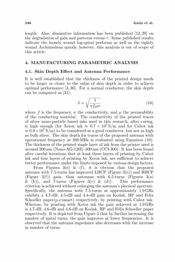
From Figures 3(e) & (f), it is obvious that the proposedantenna with 7.5-turns has improved LHCP (Figure 3(e)) and RHCP(Figure 3(f)) gain, than antennas with 6.5-turns (Figures 3(a)& (b)), and 7-turns (Figures 3(c) & (d)). This performancecriterion is achieved without enlarging the antenna’s physical aperture.Specifically, the antenna with 7.5-turns at approximately 1.9 GHzexhibits a 4.7-dB, 4.5-dB and 4.4-dB gain on Kodak, HP and FelixSchoeller paper(p e:smart) respectively, by printing with Cabot ink.Whereas, by printing with Xerox ink the gain achieved at 1.9GHzis 4.7-dB, 4.6-dB and 4.6-dB on Kodak, HP and Felix Schoeller paperrespectively. It is depicted from Figure 3 that by further increasing thenumber of spiral turns, the gain improves at lower frequencies. It isobserved that the antenna impedance also decreases with the increasein number of turns.
Progress In Electromagnetics Research, Vol. 130, 2012 247
(a) (b)
(c) (d)
(e) (f)
Figure 3. Simulated 3D LHCP & RHCP gain radiation patterns ofantennas with 6.5, 7 and 7.5-turns.
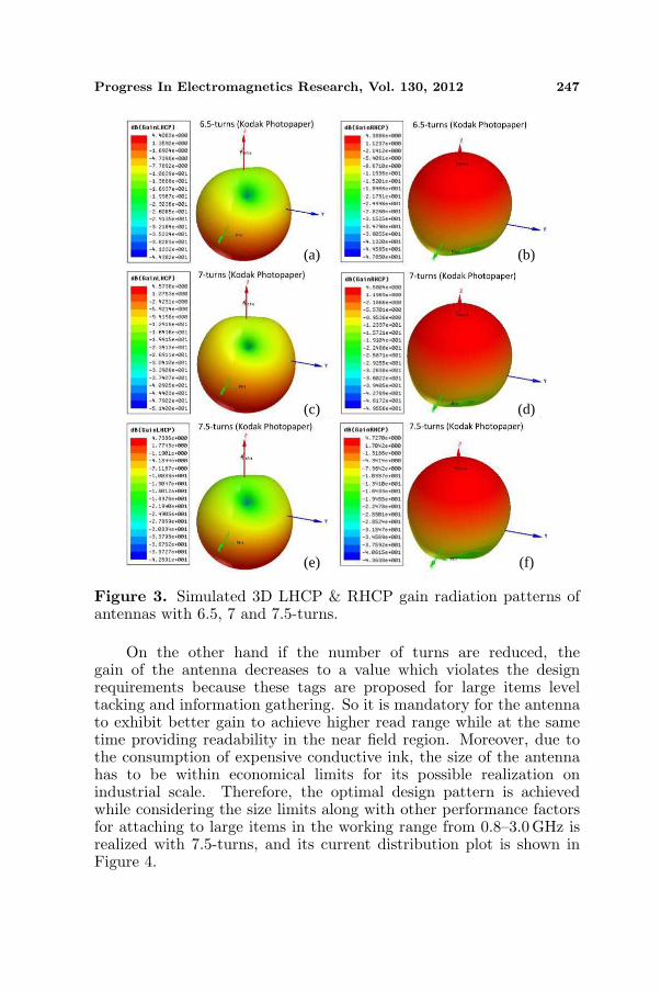
On the other hand if the number of turns are reduced, thegain of the antenna decreases to a value which violates the designrequirements because these tags are proposed for large items leveltacking and information gathering. So it is mandatory for the antennato exhibit better gain to achieve higher read range while at the sametime providing readability in the near field region. Moreover, due tothe consumption of expensive conductive ink, the size of the antennahas to be within economical limits for its possible realization onindustrial scale. Therefore, the optimal design pattern is achievedwhile considering the size limits along with other performance factorsfor attaching to large items in the working range from 0.8–3.0 GHz isrealized with 7.5-turns, and its current distribution plot is shown inFigure 4.
248 Amin et al.
Figure 4. The current distribution of proposed antenna at 1.9GHz.
(a) (b)
(c)(d)(e)(f)
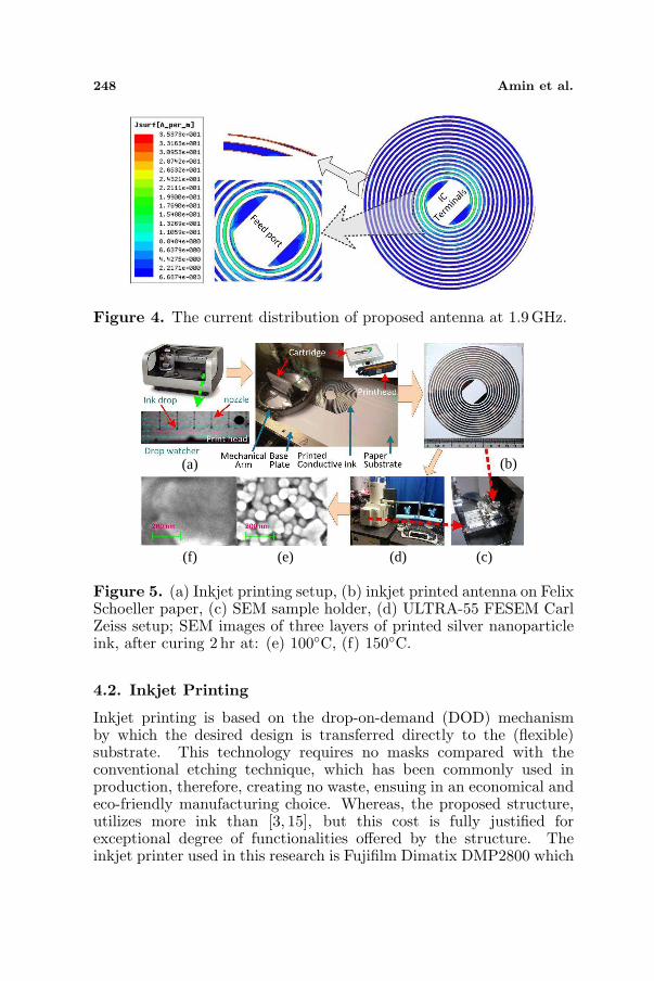
Figure 5. (a) Inkjet printing setup, (b) inkjet printed antenna on FelixSchoeller paper, (c) SEM sample holder, (d) ULTRA-55 FESEM CarlZeiss setup; SEM images of three layers of printed silver nanoparticleink, after curing 2 hr at: (e) 100C, (f) 150C.
4.2. Inkjet Printing
Inkjet printing is based on the drop-on-demand (DOD) mechanismby which the desired design is transferred directly to the (flexible)substrate. This technology requires no masks compared with theconventional etching technique, which has been commonly used inproduction, therefore, creating no waste, ensuing in an economical andeco-friendly manufacturing choice. Whereas, the proposed structure,utilizes more ink than [3, 15], but this cost is fully justified forexceptional degree of functionalities offered by the structure. Theinkjet printer used in this research is Fujifilm Dimatix DMP2800 which
Progress In Electromagnetics Research, Vol. 130, 2012 249
is a tabletop printer as showed in Figure 5(a). It employs one userfillable piezo-based inkjet print cartridge that has 16 nozzles in a singlerow with the spacing between two consecutive nozzles is 254µm, andthe substrate is held by vacuum plate. Figure 5(a) also shows thedrop watcher view of ink drops of 10 pl in volume are ejecting out ofDMC-11610 print cartridge which can be filled upto 1.5 ml.
The antenna structure on Felix Schoeller paper is showed inFigure 5(b) by using Cabot conductive ink having silver solid loadingof 19–21 wt%. Furthermore, printing parameters are optimized for allthe three paper substrate types using Xerox conductive ink havingsilver loading of 40 wt%. The optimized jetting voltage realized forboth inks is 16–20V with the velocity of around 5 m/s. The nozzletemperature is kept at room temperature, and the substrate vacuumplate, which is temperature controllable, is maintained at 40C whileprinting with either ink. In order to keep the consistency for performingin-depth analysis, each combination is printed with 20 micron dropspacing and print resolution of 1270 dpi. The printer is equipped withFiducial Camera, which provided the ease of substrate alignment usingreference marks, and positioning a print origin or reference point tomatch substrate placement. Furthermore, it is used for evaluationof features and locations along with inspection and image capture ofprinted pattern or drops.
Two different sintering processes are evaluated after drying of inkon the substrate, first one is the prevalent method and the other is
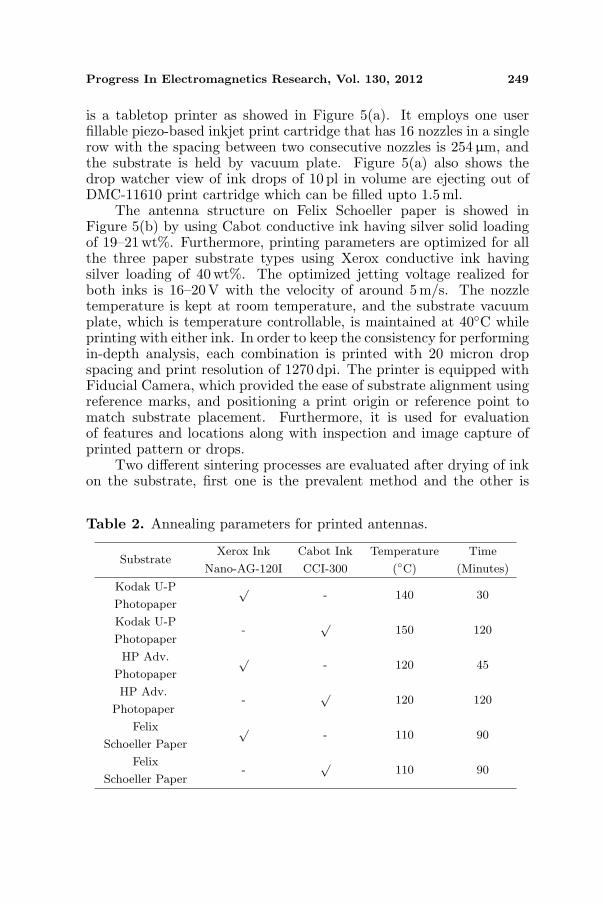
Table 2. Annealing parameters for printed antennas.
SubstrateXerox Ink
Nano-AG-120I
Cabot Ink
CCI-300
Temperature
(C)
Time
(Minutes)
Kodak U-P
Photopaper
√- 140 30
Kodak U-P
Photopaper-
√150 120
HP Adv.
Photopaper
√- 120 45
HP Adv.
Photopaper-
√120 120
Felix
Schoeller Paper
√- 110 90
Felix
Schoeller Paper-
√110 90

250 Amin et al.
“PulseForge Technology” [32]. In the first approach sintering is carriedout in the oven with ventilation system at different temperature andtime (as mentioned in Table 2), depending upon the combination ofink and substrate, for sufficiently curing, removing the excess solventand material impurities from the depositions.
The printed samples are also sintered through “PulseForgeTechnology” by Novacentrix USA, in order to demonstrate sinteringand annealing for high-speed roll-to-roll manufacturing often inambient air (and is capable of up to 1000 feet per minute). Thisapproach enables the use of ultra low temperature and flexiblesubstrates such as paper substrate, which cannot be annealed at hightemperatures.
The characterization of the printed structures is carried out underULTRA-55 Field Emission Scanning Electron Microscope from CarlZeiss NTS showed in Figures 5(c) & (d). Figures 5(e) & (f) show theSEMs for elaborating the difference between the heating temperatures.At high temperature or by “PulseForge Technology”, an almost solidmetal conductor is formed so providing a percolation channel for theconduction of electrons throughout the material without obstruction.The sintering process also provides the derived benefit of increasingthe bonding of the deposition with the paper substrate.
5. FIELD & CIRCUIT CONCEPTS PARAMETRICANALYSIS
A set of precise and thorough methods for evaluation of the reliabilityparameters and characterization of the proposed fabricated antennaon different paper substrates are implemented. Firstly, five identicalstructures are printed for each arrangement of ink and papersubstrate. Secondly, in this study, an experimental methodology forthe characterization of the impedance of the balanced tag antennais implemented along with the balun structure. The balanced tagantenna is considered as a two-port network and the impedance ofthe antenna is characterized using network parameters. The antennais connected to the two ports of a vector network analyzer through atest fixture mentioned in detail in [33]. The influence of the test fixtureis deembedded by using a port-extension technique and the antennaimpedance can be extracted directly from the measured parameters.Whereas, the broadband balun transforms the unbalanced coaxialmode into balanced two-wire transmission line mode that fed the spiralantenna. The accuracy of the measurements is increased if all errorsup to the measuring instrument tip are eliminated [34]. This includesinternal VNA errors after the sampler, the cables along with their tips
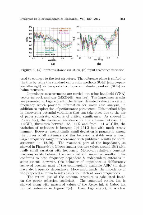
Progress In Electromagnetics Research, Vol. 130, 2012 251
(a) (b)
Figure 6. (a) Input resistance variation, (b) input reactance variation.
used to connect to the test structure. The reference plane is shifted tothe tips by using the standard calibration methods SOLT (short-open-load-through) for two-ports technique and short-open-load (SOL) forbalun structure.
Impedance measurements are carried out using handheld (VNA)vector network analyzer (MS2026B, Anritsu). The impedance graphsare presented in Figure 6 with the largest deviated value at a certainfrequency which provides information for worst case analysis, inaddition to exploration of performance parameters. This method helpsin discovering potential variations that can take place due to the useof paper substrate, which is of critical significance. As showed inFigure 6(a), the measured resistance for the antenna between 1.1–1.4GHz, fluctuates between 158–144 Ω and from 1.41–3.0 GHz, thevariation of resistance is between 146–154 Ω but with much steadymanner. However, exceptionally small deviation is pragmatic amongthe curves of all antennas and this behavior is stable over a muchlarger frequency range in accordance with published results for spiralstructures in [12, 29]. The reactance part of the impedance, asshowed in Figure 6(b), follows smaller positive values around 15 Ω withreally small variation with frequency. Moreover, relatively constantharmony exists between the computed and measured results. Thisconforms to both frequency dependent & independent antennas insome extent; however, this behavior of impedance is deliberatelyachieved because most of the commercially available ASIC till datehave also frequency dependence. More importantly, the impedance ofthe proposed antenna besides easier to match at lower frequencies.
The return loss of the antenna structure is calculated basedon the power reflection coefficient. The computed return loss isshowed along with measured values of the Xerox ink & Cabot inkprinted antennas in Figure 7(a). From Figure 7(a), it is clear
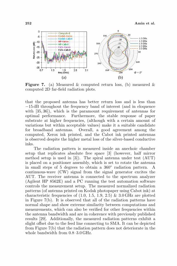
252 Amin et al.
(a) (b)
Figure 7. (a) Measured & computed return loss, (b) measured &computed 2D far-field radiation plots.
that the proposed antenna has better return loss and is less than−15 dB throughout the frequency band of interest (and in eloquencewith [35, 36]), which is the paramount requirement of antennas foroptimal performance. Furthermore, the stable response of papersubstrate at higher frequencies, (although with a certain amount ofvariations but within acceptable values) make it a suitable candidatefor broadband antennas. Overall, a good agreement among thecomputed, Xerox ink printed, and the Cabot ink printed antennasis observed despite the higher metal loss of the silver-based conductiveinks.
The radiation pattern is measured inside an anechoic chambersetup that replicates absolute free space [3] (however, half mirrormethod setup is used in [3]). The spiral antenna under test (AUT)is placed on a positioner assembly, which is set to rotate the antennain small steps of 5 degrees to obtain a 360 radiation pattern. Acontinuous-wave (CW) signal from the signal generator excites theAUT. The receiver antenna is connected to the spectrum analyzer(Agilent HP 8562E) and a PC running the test automation softwarecontrols the measurement setup. The measured normalized radiationpatterns (of antenna printed on Kodak photopaper using Cabot ink) atcharacteristic frequencies of (1.0, 1.5, 1.9, 2.5) & 3.0GHz are plottedin Figure 7(b). It is observed that all of the radiation patterns havenormal shape and show extreme similarity between computations andmeasurements, which can also be verified for other frequencies withinthe antenna bandwidth and are in coherence with previously publishedresults [29]. Additionally, the measured radiation patterns exhibit aslight offset due to the feed line connecting to SMA. It can be depictedfrom Figure 7(b) that the radiation pattern does not deteriorate in thewhole bandwidth from 0.8–3.0 GHz.
Progress In Electromagnetics Research, Vol. 130, 2012 253
6. CONCLUSION
In this paper, it is the first time to propose wideband spiral antennasfabricated on paper substrate for simultaneously implementing a widerange of different modules in addition to, RFID tag. It is noted thatadjusting the gap between the adjacent tracks to create the spiralarms leads to a larger number of turns within the same aperturesize. All the previously published relevant work in contrast to theproposed approach, is focused on complex techniques, to make suchantennas using nonflexible or contaminated substrates, which neithercan be implemented with roll-to-roll printing nor suitable for eco-friendly applications. Although the presented research is specific toinkjet printed Archimedean spiral antennas, the same approach can beapplied to other antennas made of printed strips, to form modules for“green” electronics.
ACKNOWLEDGMENT
The author would like to thank Peter Fuks in school of electrical en-gineering at KTH who generously provided research facilities. Thiswork was financially supported by Vinnova (The Swedish Governmen-tal Agency for Innovation Systems) through the Vinn Excellence cen-ters program.
REFERENCES
1. Kim, M., K. Kim, and N. Chong, “RFID based collision-free robotdocking in cluttered environment,” Progress In ElectromagneticsResearch, Vol. 110, 199–218, 2010.
2. Garcia, J. A., L. Cabria de Juan, R. Marante, L. Rizo, andA. Mediavilla, “An unbiased dual-mode mixing antenna forwireless transponders,” Progress In Electromagnetics Research,Vol. 102, 1–14, 2010.
3. Amin, Y., Q. Chen, H. Tenhunen, and L. R. Zheng, “Performance-optimized quadrate bowtie RFID antennas for cost-effective andeco-friendly industrial applications,” Progress In ElectromagneticsResearch, Vol. 126, 49–64, 2012.
4. Tiang, J.-J., M. T. Islam, N. Misran, and J. S. Mandeep, “Circularmicrostrip slot antenna for dual-frequency RFID application,”Progress In Electromagnetics Research, Vol. 120, 499–512, 2011.
5. Meng, Y. S. and Y. H. Lee, “Investigations of foliage effect on
254 Amin et al.
modern wireless communication systems: A review,” Progress InElectromagnetics Research, Vol. 105, 313–332, 2010.
6. Li, X., J. Liao, Y. Yuan, and D. Yu, “Eye-shaped segmentedreader antenna for near-field UHF RFID applications,” ProgressIn Electromagnetics Research, Vol. 114, 481–493, 2011.
7. Alejos, A. V., M. G. Sanchez, I. Cuinas, and J. C. G. Valladares,“Sensor area network for active RTLS in RFID trackingapplications at 2.4 GHz,” Progress In Electromagnetics Research,Vol. 110, 43–58, 2010.
8. Jamlos, M. F., A. R. B. Tharek, M. R. B. Kamarudin,P. Saad, O. A. Aziz, and M. A. Shamsudin, “Adaptive beamsteering of RLSA antenna with RFID technology,” Progress InElectromagnetics Research, Vol. 108, 65–80, 2010.
9. Panda, J. R. and R. S. Kshetrimayum, “A printed2.4GHz/5.8 GHz dual-band monopole antenna with a protrudingstub in the ground plane for WLAN and RFID applications,”Progress In Electromagnetics Research, Vol. 117, 425–434, 2011.
10. Sim, Z. W., R. Shuttleworth, M. J. Alexander, and B. D. Grieve,“Compact patch antenna design for outdoor RF energy harvestingin wireless sensor networks,” Progress In ElectromagneticsResearch, Vol. 105, 273–294, 2010.
11. Jamlos, M. F., A. R. B. Tharek, M. R. B. Kamarudin, P. Saad,M. A. Shamsudin, and A. M. M. Dahlan, “A novel adaptive Wi-Fi system with RFID technology,” Progress In ElectromagneticsResearch, Vol. 108, 417–432, 2010.
12. Guraliuc, A. R., R. Caso, P. Nepa, and J. L. Volakis, “Numericalanalysis of a wideband thick archimedean spiral antenna,” IEEEAntennas and Wireless Propagation Letters, Vol. 11, 168–171,2012.
13. Ramos, A., A. Lazaro, D. Girbau, and R. Villarino, “Time-domainmeasurement of time-coded UWB chipless RFID tags,” ProgressIn Electromagnetics Research, Vol. 116, 313–331, 2011.
14. Chen, A.-X., T.-H. Jiang, Z. D. Chen, and D. Su, “A novellow-profile wideband UHF antenna,” Progress In ElectromagneticsResearch, Vol. 121, 75–88, 2011.
15. Amin, Y., Q. Chen, H. Tenhunen, and L. R. Zheng, “Evolutionaryversatile printable RFID antennas for “Green” electronics,”Journal of Electromagnetic Waves and Applications, Vol. 26,Nos. 2–3, 264–273, 2012.
16. Mahmoud, K. R., “Design optimization of a bow-tie antennafor 2.45 GHz RFID readers using a hybrid BSO-NM algorithm,”

Progress In Electromagnetics Research, Vol. 130, 2012 255
Progress In Electromagnetics Research, Vol. 100, 105–117, 2010.17. Filipovic, D. S. and J. L. Volakis, “Broadband meanderline slot
spiral antenna,” 2002 IEE Proceedings — Microwaves, Antennasand Propagation, 98–105, 2002.
18. Zhu, Y.-Z. and J.-D. Xu, “Design of two-arm conical spiralantenna for low elevation angle communication,” Journal ofElectromagnetic Waves and Applications, Vol. 24, Nos. 5–6, 785–794, 2010.
19. Liao, W.-J., S.-H. Chang, and L.-K. Li, “A compact planarmultiband antenna for integrated mobile devices,” Progress InElectromagnetics Research, Vol. 109, 1–16, 2010.
20. Tze-Meng, O., K. G. Tan, and A. W. Reza, “A dual-band omni-directional microstrip antenna,” Progress In ElectromagneticsResearch, Vol. 106, 363–376, 2010.
21. Secmen, M. and A. Hizal, “A dual-polarized wide-band patchantenna for indoor mobile communication applications,” ProgressIn Electromagnetics Research, Vol. 100, 189–200, 2010.
22. Ou Yang, J., S. Bo, J. Zhang, and F. Yang, “A low-profileunidirectional cavity-backed log-periodic slot antenna,” ProgressIn Electromagnetics Research, Vol. 119, 423–433, 2011.
23. De Cos, M. E., Y. Alvarez Lopez, R. C. Hadarig, and F. Las-Heras,“Flexible uniplanar artificial magnetic conductor,” Progress InElectromagnetics Research, Vol. 106, 349–462, 2010.
24. Chen, J., G. Fu, G.-D. Wu, and S.-X., Gong, “A novelbroadband circularly polarized irregular slot antenna,” Journalof Electromagnetic Waves and Applications, Vol. 24, Nos. 2–3,413–421, 2010.
25. Richard, C. J., Antenna Engineering Handbook, McGraw-Hill Inc.,New York, 1992.
26. Balanis, C. A., Antenna Theory, John Wiley and Sons Inc., NewJersey, 2005.
27. Lin, D.-B., I.-T. Tang, and C.-C. Wang, “UHF RFID H-shapedtag antenna using microstrip feed design on metallic objects,”Journal of Electromagnetic Waves and Applications, Vol. 25,No. 13, 1828–1839, 2011.
28. Hsu, H.-T., F.-Y. Kuo, and C.-H. Chang, “Application ofquasi log- periodic antenna for UHF passive RFID tag designfeaturing constant power transmission coefficient over broadbandoperation,” Journal of Electromagnetic Waves and Applications,Vol. 24, Nos. 5–6, 575–586, 2010.
29. Chen, T.-K. and G. H. Huff, “Stripline-fed archimedean spiral

256 Amin et al.
antenna,” IEEE Antennas and Wireless Propagation Letters,Vol. 10, 346–349, 2011.
30. Huang, Y. and K. Boyle, Antennas from Theory to Practice, JohnWiley & Sons Ltd., New York, 2008.
31. Da Silveira, F. E. M. and J. A. S. Lima, “Skin effect fromextended irreversible thermodynamics perspective,” Journal ofElectromagnetic Waves and Applications, Vol. 24, Nos. 2–3, 151–160, 2010.
32. PulseForge Technology, Available at www.novacentrix.com.33. Kuo, S.-K., J.-Y. Hsu, and Y.-H. Hung, “Analysis and design of
an UHF RFID metal tag using magnetic composite material assubstrate,” Progress In Electromagnetics Research B, Vol. 24, 49–62, 2010.
34. Zhao, W., Y.-J. Zhao, and H.-B. Qin, “Calibration of the three-port VNA using the general 6-term error model,” Journal ofElectromagnetic Waves and Applications, Vol. 24, Nos. 2–3, 319–326, 2010.
35. Schreider, L., X. Begaud, M. Soiron, B. Perpere, andC. Renard, “Broadband Archimedean spiral antenna above aloaded electromagnetic band gap substrate,” IET Microwaves,Antennas & Propagation, Vol. 1, No. 1, 212–216, 2007.
36. Bell, J. M. and M. F. Iskander, “A low-profile Archimedeanspiral antenna using an EBG ground plane,” IEEE Antennas andWireless Propagation Letters, Vol. 3, 223–226, 2004.