Graphene Research and Advances Report June 2019 · focuses on two of the six areas of strength...
19
Graphene Research and Advances Report June 2019 Johan Ek Weis, Sophie Charpentier, Camilla Johansson 19 June 2019
Transcript of Graphene Research and Advances Report June 2019 · focuses on two of the six areas of strength...
Graphene Research and Advances
Report June 2019
Johan Ek Weis, Sophie Charpentier, Camilla Johansson
19 June 2019
SIO Grafen – Graphene Research and Advances
SIO Grafen | [email protected] | siografen.se
2
Introduction
SIO Grafen’s Research Intelligence Report Series, published twice a year, aims to highlight
some of the most interesting research findings on graphene that have emerged during the last
few months. The scope of the reports has been updated this year. Instead of discussing a few
of the most interesting articles from the last six months in each area of strength, this report
focuses on two of the six areas of strength within SIO Grafen; electronics and coatings. In
addition to the usual state-of-art research presentation, the report also includes a discussion of
the patent landscape within these areas and the graphene field in general.
In the last few years, there has been a strong interest from the Swedish industry to incorporate
graphene in a variety of applications, specifically in the areas of electronics and coatings.
Researchers at Swedish universities also have corresponding expertise, especially in the area
of electronics. These matching interests have resulted in many innovation projects funded
through SIO Grafen, with 30 and 31 projects, respectively, within the coatings and electronics
areas of strength. In total 89 innovations projects have been started within SIO Grafen since
the beginning 5 years ago. A complete list of these can be found on the SIO Grafen web.

SIO Grafen – Graphene Research and Advances
SIO Grafen | [email protected] | siografen.se
3
Content:
Introduction ................................................................................................................................ 2
Content: ...................................................................................................................................... 3
State-Of-Art Research - Electronics ........................................................................................... 4
Band Structure Engineering .................................................................................................... 4
Graphene Inks ......................................................................................................................... 6
State-Of-Art Research - Coatings .............................................................................................. 8
Statistics of Scientific Publications .......................................................................................... 10
Patents ...................................................................................................................................... 12
Potential Market ....................................................................................................................... 16
Summary .................................................................................................................................. 17
SIO Grafen – Graphene Research and Advances
SIO Grafen | [email protected] | siografen.se
4
State-Of-Art Research - Electronics
Electronics based on silicon technology has been developed for several decades with
investments of billions of dollars. However, the evolution of this technology is reaching its
fundamental limitations. The vision for technology based on 2D materials is not to replace
silicon, but rather to coexist. Although there are many ideas and a lot of research being done,
there is no consensus on exactly which role the 2D materials will have in this hybrid platform.
A recent roadmap highlights that interconnects, diffusion barriers, and access resistors for
memory elements are more likely than the replacement of logic units.1
This hybrid technology requires that the growth of the 2D materials is compatible with
silicon-based technology, which still is a challenge. However, 2D materials can also directly
be incorporated into new technologies such as for Internet of Things, wearables etc. Many of
this type of technologies relies on the application of inks of graphene or other 2D materials.
Some interesting new findings in this area will be discussed further down.
Band Structure Engineering
The band gap is an important property of materials for electronics and the ability to control
the band gap opens the possibility to many potential devices. A few different methods to
control the band structure of graphene were recently demonstrated. Other more established
techniques to tune the band structure have been investigated previously in addition to these
methods, such as for example chemical doping or especially electrostatic gating.
Magic Angles and Pressure Control
Monolayers of graphene can be stacked on each other to achieve new properties. Two layers
form what is known as a Moiree pattern with varying properties depending on the angle
between the two layers. This is a topic which has received significant attention in the research
community the last few years.
It was found last year that two monolayers of graphene with a twist angle of 1.1° becomes
superconducting.2 However, this twist angle needs to be very precise and can be difficult to
maintain between the layers. A recent study found that the angle can be increased, and even
tuned, by varying the interlayer spacing between the layers.3 This separation between the
layers was controlled by applying a hydrostatic pressure.
SIO Grafen – Graphene Research and Advances
SIO Grafen | [email protected] | siografen.se
5
This is not only interesting for the potential of making superconducting devices but is also an
interesting structure for researchers to learn more about superconductivity. Whereas the
structure of superconductors with similar behaviour consist of complex molecules, twisted
bilayer graphene is a relatively simple structure which is much easier both to model and to
change the doping of.
Nanolithography
It has long been known that the band structure of graphene can be tuned by patterning the
structure. However, this requires control on a length scale of 10 nm, which is very
challenging. Nevertheless, this control has now been demonstrated in a recent study.4 The
graphene was patterned by nanolithography, where the ballistic transport properties of
graphene were maintained also after structuring. One of the keys to achieve this was to
encapsulate the graphene in hexagonal boron nitride (BN), which has proven to be an
excellent material for protecting graphene.
This is an important milestone as it shows that a top-down process, such as lithography, can
be used to manipulate the band structure of graphene without sacrificing the excellent
transport properties of the material.
Nanoribbons
A band gap can be introduced in graphene by making the structure very narrow. Graphene
nanoribbons with widths less than 50 µm are therefore discussed as potential key components
in future electronics. Researchers at Lund and Linköping (together with colleagues in
Germany) recently demonstrated manufacturing of this kind of graphene using a scalable
method.5 Both ribbons with armchair and zigzag edges were thoroughly characterised. It was
found that the quality of the zigzag ribbons was better than the armchair ones. The higher
resistance of the armchair ribbons indicated a possible opening of a band gap, which can be
utilized in potential devices.
Heterostructures
There are many different types of two-dimensional materials, as discussed in previous issues
of these research intelligence reports. These materials have different properties and are suited
for diverse applications. It has long been envisioned that these can be combined by stacking
them on top of each other in order to create new devices. These stacks are often labelled
SIO Grafen – Graphene Research and Advances
SIO Grafen | [email protected] | siografen.se
6
heterostructures. The close proximity between the different layers and materials will then
influence the properties of the individual pristine materials. This aspect is increasingly being
investigated.
A new study has focused on a three-layer structure consisting of graphene sandwiched
between two sheets of BN.6 It was found that one Moiree superlattice form from the graphene
and the top BN layer, and another different Moiree superlattice from the graphene and the
bottom BN layer. These two superlattices can also result in a third even larger superlattice,
which shows that the band structure of three-layer systems can be engineered to result in new
electronic properties.
Graphene Inks
Printed and flexible electronics opens the possibility to develop new applications, for
example, for internet of things and wearable devices. This type of electronics can be printed
from conductive inks to create, for example, sensors, antennas, transistors and RFID tags.
Traditional inks use metal nanoparticles in order to be electrically conductive, but these
materials can be expensive and easily oxidised.
A new study shows how graphene inks can be manufactured using a non-toxic,
environmentally friendly and sustainable method.7 The method uses a cellulose derived
solvent to develop graphene inks with high concentration of graphene (10 mg/mL) which was
further concentrated (to 70 mg/mL) for screen printing. The performance of the ink was
demonstrated in antennas, battery-free wireless body temperature sensor, RFID tags and RF
energy harvesting system for powering battery-free devices.
A group from KTH recently demonstrated a technique which can deposit inkjet printed
graphene devices on a wide range of substrates, such as plastics, paper, wood and leather.8
The technique relies on first printing the graphene components on a copper substrate and then
transferring them onto the target material. The technique works on three-dimensional objects
like cylinders, spheres and cubes and was even shown on fruits and plants.
Graphene can also be coated on textiles. A recent study by the university of Borås showed
that graphene oxide can be coated on polyester fabrics.9 It was found that an additional
surface treatment of chitosan or hexadecylpyridinium chloride significantly improved the
electrical and thermal performance.

SIO Grafen – Graphene Research and Advances
SIO Grafen | [email protected] | siografen.se
7
Another recent report investigated graphene for use as electronic tattoos.10 An electrically
conducting path is formed by the graphene. As this conductivity is sensitive to external strain,
matrix swelling induced by high humidity and temperature variations, a multifunctional
sensor could be designed. The electronic tattoo was additionally made to be self-healing.

SIO Grafen – Graphene Research and Advances
SIO Grafen | [email protected] | siografen.se
8
State-Of-Art Research - Coatings
Graphene is strong, chemically inert, impermeable to gas and stable in ambient conditions up
to 400°C. It holds great promises to provide long-lasting protection against corrosion and
friction. It is also very thin, making it particularly attractive for surface coating applications.
Self-Healing Oil Barrier Coating
It is not new for different types of fluid-like media to be used as self-healing coatings. Low
viscosity liquids can readily flow and reconnect, which in principle is good for self-healing,
but unfortunately prevents them from being stable coatings, for example on vertical surfaces.
On the contrary, high viscosity liquid present the exact opposite advantage/disadvantage. In a
recent article, researchers show how microcapsules of graphene oxide can be used to improve
the self-healing properties of a low-viscosity silicone oil barrier coating.11 In such a hybrid
coating, the adherence of the low-viscosity oil film on the surface is ensured using the
microcapsules as thickeners. The graphene oxide-based microcapsules are sufficiently robust
and resilient during the handling, while being extremely light, an addition of only 5 wt.%
increases the viscosity of silicon oil by a factor of 1000.
Novel Wearable Devices
Graphene could also have a strong impact in the field of wearable electronics, thanks to its
flexibility and unique electrical properties. In a recent report, researchers developed a way to
dye polyester fabric using graphene and other two-dimensional materials low-cost, sustainable
and scalable inks.12 Since the process can be used with a variety of material, several dyed
fabrics with different properties can be overlaid to create electronic circuits, for example, an
all-textile-based capacitive heterostructure as demonstrated in the report. The same technique
could also be used to produce a variety of devices for healthcare monitoring systems, flexible
circuits, etc.
Oxygen Barrier
In a recent article, researchers showed how a thin coating of reduced graphene oxide can
considerably reduce the risk for fire in a Li-ion battery.13 Lithium batteries suffer from
thermal instability, and under high heat can even catch fire. This is caused by a decomposition
of the cathode, which usually contains an oxide, releasing oxygen that can combine with other
flammable products. In their experiment, researchers significantly reduced the release of the
SIO Grafen – Graphene Research and Advances
SIO Grafen | [email protected] | siografen.se
9
oxygen by a LiCoO-based cathode by coating the LiCoO particles with a thin layer of reduced
graphene oxide. The wrapped cathode battery was tested and performed even better than
conventional lithium batteries in rapid cycling tests, showing the effectiveness of the coating
in improving this type of batteries.
Water Capture
A new study showed that graphene-based composite foam can be used to harvest water from
the atmosphere using solar energy.14 The composite foam consist of several materials,
insuring the entire cycle of usage of the foam. The water vapor is absorbed and retained by
LiCl and poly(vinyl alcohol) (PVA) respectively, whereas reduced graphene oxide embedded
in the foam, not only support the skeleton to facilitate water evaporation but also act as a
solar-to-thermal transformer. It has a capability of 0.23 and 1.15 g g−1 (grams of water per
grams of foam) in a typical 2 h capture − 2 h release cycle when the corresponding relative
humidity values are 30 and 90% during water capture. This hybrid foam is reusable, portable
(i.e. low density), superelastic and it could therefore be compressed and easily transported to
regions where it is most needed.
Elastic in Space
In another recent study, a graphene based foam showed stable mechanical properties in an
unprecedently wide range of temperature.15 This material, called 3D Graphene foam, is the
first material ever reported with high elasticity at liquid helium temperature (4 K). Based both
on experiments and modelling results, it was concluded that the key to this high elasticity is
not only the unique architecture of the graphene sheets in the foam mediated by cross-linking
between the sheets, but the intrinsic elastic/flexibility properties of individual graphene. These
results suggest possible applications for such materials at extremely low temperatures, such as
those in outer space.
SIO Grafen – Graphene Research and Advances
SIO Grafen | [email protected] | siografen.se
10
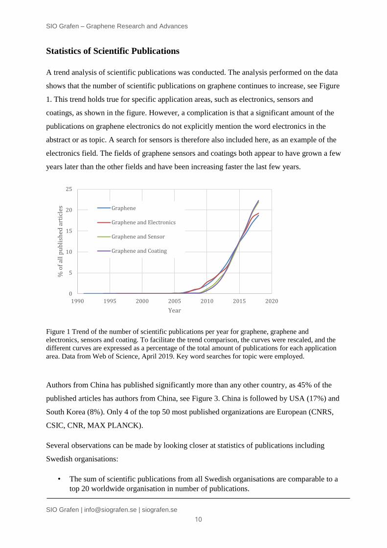
Statistics of Scientific Publications
A trend analysis of scientific publications was conducted. The analysis performed on the data
shows that the number of scientific publications on graphene continues to increase, see Figure
1. This trend holds true for specific application areas, such as electronics, sensors and
coatings, as shown in the figure. However, a complication is that a significant amount of the
publications on graphene electronics do not explicitly mention the word electronics in the
abstract or as topic. A search for sensors is therefore also included here, as an example of the
electronics field. The fields of graphene sensors and coatings both appear to have grown a few
years later than the other fields and have been increasing faster the last few years.
Figure 1 Trend of the number of scientific publications per year for graphene, graphene and
electronics, sensors and coating. To facilitate the trend comparison, the curves were rescaled, and the
different curves are expressed as a percentage of the total amount of publications for each application
area. Data from Web of Science, April 2019. Key word searches for topic were employed.
Authors from China has published significantly more than any other country, as 45% of the
published articles has authors from China, see Figure 3. China is followed by USA (17%) and
South Korea (8%). Only 4 of the top 50 most published organizations are European (CNRS,
CSIC, CNR, MAX PLANCK).
Several observations can be made by looking closer at statistics of publications including
Swedish organisations:
• The sum of scientific publications from all Swedish organisations are comparable to a
top 20 worldwide organisation in number of publications.
0
5
10
15
20
25
1990 1995 2000 2005 2010 2015 2020
% o
f al
l pu
bli
shed
art
icle
s
Year
Graphene
Graphene and Electronics
Graphene and Sensor
Graphene and Coating
SIO Grafen – Graphene Research and Advances
SIO Grafen | [email protected] | siografen.se
11
– This is valid for all graphene publications, as well as for graphene in
electronics, sensors and coatings.
• Similarly, Sweden is ranked in the top 20 compared to other countries.
• Swedish organisations mainly collaborate with Chinese, German and American
organisations.
• Four universities stand out when comparing the number of published articles by
Swedish organisations. Chalmers, Linköping University, Uppsala University and KTH
have each published approximately 0.2 % of the worldwide number of publications.
• SHT Smart High Tech is noteworthy among Swedish companies with a significant
amount of publications.
SIO Grafen – Graphene Research and Advances
SIO Grafen | [email protected] | siografen.se
12
Patents
The patent search was performed using the patent database Orbit Intelligences. This is a
global patent database comprising more than 50 million patent families (comprising more
than 100 million patent and patent applications). Please note that there are patents and patent
applications which due to different reasons do not appear when performing this search. For
example, this may be due to that a patent application do not become public until 18 months
after filling. Other reasons may be due to mistakes which have been made when translating a
patent or a patent application.
In order to find patents related to graphene, the search string included not only the word
“graphene” but other expressions such as “two dimension”.a This search string was used for
searches within the full text of the patents and patent applications. In addition, specific
keywords searches of titles, abstracts and claims were used for area specific searches.b
The trends for the number of patent families which have been filed every year are very similar
to the trends for scientific publications, c.f. Figure 1 with Figure 2. For example, it can be
seen that electronics was an early area both in scientific publications as for patents or patent
applications.
The distribution of legal status of the patents and patent applications is very similar for all
graphene patent families and the ones within the subfields of electronics, sensors and
coatings. Approximately 40% of the filed and published applications have been granted and
40% are still pending, whereas approximately 5% have been revoked, 1% expired and 10%
lapsed. The fact that as many as 40% of the patent applications are pending is a sign that the
area has been growing quickly the last years. There are most probably more pending patent
applications than what is visible in these statistics as the patent applications filed the last 18
months don’t need to be public yet.
a The following search string has been used: (graphene) OR ((two 2W dimension+) 5W (carbon OR material)).
b The following keywords were used for searches within titles, abstracts and claims: (electronic+), (sensor+) and
(coating+).

SIO Grafen – Graphene Research and Advances
SIO Grafen | [email protected] | siografen.se
13
Figure 2 Trend of the number of patent families files as a function of the priority year (year for filing
the first patent application of the family) for graphene, graphene and electronics, sensors and coating.
To facilitate the trend comparison, the curves were rescaled, and the different curves are expressed as
a percentage of the total amount of patent families for each application area.
Close to 39% of all graphene patent families has one member which is filed and published in
China, either direct or via a worldwide Patent Cooperation Treaty (PCT)-applicationc. This is
significantly more than the second largest, USA with 13%. These two countries together hold
half of all the graphene patents. There are also a significant number of patent and patent
applications published at the Japanese (9%) and South Korean (9%) patent offices.
Consequently, almost 70% of all graphene patents and applications are published in these four
countries. Although this appear as a very high number, it can be compared with solar cells
where over 90% of all published patents and patent applications are published in the same
four countries, China (55%), Japan (20%), South Korea (11%) and USA (6%).
Approximately 6% of the graphene patents and patent applications are published at the
European patent office. While this is a low percentage, it can be compared with only 1% for
c A PCT-application is an international patent application which makes it possible to seek patent protection for
an invention simultaneously in a large number of countries by filing a single application instead of filing several
separate national or regional applications. The granting of patents remains under the control of the national or
regional patent Offices in what is called the “national phase”.
0
2
4
6
8
10
12
14
16
18
20
1990 1995 2000 2005 2010 2015 2020
% o
f al
l pat
ents
Year
Graphene
Graphene and Electronic
Graphene and Sensor
Graphene and Coating

SIO Grafen – Graphene Research and Advances
SIO Grafen | [email protected] | siografen.se
14
solar cells. In addition to these, 10% of all graphene patent applications are worldwide PCT
applications.
Although China dominates the number of published patents and patent applications, very few
Chinese organisations apply for patents outside of China. A study from last year, which
investigated patents published 1985-2016, found that only 2.3% of the Chinese patents have
corresponding patents in other countries.16 The study compared the patent application flow in
the top five countries. It was found that South Korea (28%), USA (25%), Japan (32%), and
Germany (45%) applied for a significantly higher ratio of patents in the other four countries.
Figure 3 The total number of scientific publications on graphene published by organisations from
different countries compared with where patents on graphene have been filed and where the assignee
is registered. Data from Web of Science and Orbit Intelligences.
Figure 3 similarly shows that, whereas over 80 000 patents have been filed in China, Chinese
organisations have only applied for a bit more than 20 000 patents. There is a similar situation
in many countries, as can be seen in Figure 3, by comparing the red middle bar for published
patents and patent applications with the green bar on the right for how many patents or patent
application organisations registered in the different countries hold. This can be interpreted as
that the markets in these countries are interesting for foreign entities. Interestingly, this pattern
is not as significant in Germany.
0
20000
40000
60000
80000
Nu
mb
er o
f p
ub
lica
tio
ns
or
pat
etn
s
Scientific publications
Published patents or patentapplications
Patent Assignee

SIO Grafen – Graphene Research and Advances
SIO Grafen | [email protected] | siografen.se
15
Most countries have significantly more scientific publications than filed patent applications.
However, Japan and Germany are clear exceptions to this.
Most of the Chinese patents are held by universities and research institutes, whereas
enterprises are dominating in USA and South Korea.16 The study further found that the
Chinese patents were concentrated mainly on preparation, batteries and composites.
Figure 4 shows in which countries and regions the graphene patents and patent applications
have been published. It can be seen that the trend for all graphene patent families is, in
general, very similar to the trends for the subfields of electronics, sensors and coatings. The
proportion of patent families within electronics is relatively low in China (although still
highest in the world) and high in USA.
Swedish organisations have mainly been filing patent applications (which have been
published) in Europe (14%), USA (11%) and China (7%), see Figure 4. Swedish companies
here include global organisations where the Swedish branch is listed as an assignee.
Figure 4 The spread of in which countries and regions the graphene patents and patent applications
have been published, expressed as a percentage of the total amount within each area (total, electronics,
sensors and coatings). This is compared with where Swedish organisations have filed their published
patents and patent applications.
0
5
10
15
20
25
30
35
40
CN US WO JP KR EP TW DE CA IN AU BR GB SE
Per
cen
tage
of
pat
ents
Total
Electronics
Sensors
Coatings
Swedish assignees

SIO Grafen – Graphene Research and Advances
SIO Grafen | [email protected] | siografen.se
16
Potential Market
Electronics
In 2015, the worldwide semiconductor sales were $335.2 billion, with an expected compound
annual growth rate of 2.5%. In Europe, the product value generated with Micro- and Nano-
electronic components was roughly €17.8 billion in 2014, with a 7.2% decrease from prior
years. In terms of turnover, Europe is behind both Asia and North America, with European
producers having roughly 10% of the global market share (USA has 50%). The broader group
of industries, including electrical and electronic engineering, as well as radio and
telecommunications and wireless communication industries is seen as one of the most
competitive manufacturing industries in Europe by the European Commission. Specifically,
Europe has a strength in “More than Moore”-technologies and special logic applications,
which should allow the economic value of semiconductor component production to increase
significantly in the next 5 years.17
As mentioned early in the report, a purely graphene or 2D materials-based electronics is not
expected by most actors in the electronic field, and there are more opportunities using hybrid
approaches. Wafer scale integration of graphene is the main bottleneck for the integration of
graphene in this type of applications.
Coating
The overall market for coatings and paints is estimated to be €100 billion in 2014 with an
expected compound annual growth rate of ~5 % until 2020 where the value is projected to
reach V130 billion. There is a significant industrial base in Europe for coatings, varnishes and
paints. Relevant production value was on the order of €19 billion in 2014. The innovation and
patent capacity are high in Europe in this area. 17
In general, graphene flakes produced by liquid exfoliation (or other “low cost” methods) are
used for coatings applications. Also, only a small quantity of material is required to have a
strong impact. The drive to develop more environmentally friendly alternatives could also
promote the use of graphene as an additive for coatings and paints.
SIO Grafen – Graphene Research and Advances
SIO Grafen | [email protected] | siografen.se
17
Summary
Electronics and coatings are two important application areas for graphene. There is a big
potential for graphene to both supplement and improve on existing technologies, and to create
new devices, for example within wearables.
In the early days of graphene research, the vision for graphene electronics was to replace
silicon technology. The vision is now rather to tailor properties of new materials on an almost
atomic scale, for example by stacking different two-dimensional materials. Some of the
concepts for realising this were discussed in this report.
One of the potentially cheaper and easier ways to take advantage of graphene in new devices
is by using graphene inks. These consist of flakes of graphene which can be manufactured by
cheaper methods than other types of graphene (such as by chemical vapour deposition or
epitaxial growth, as discussed in earlier versions of these reports). Some recent articles,
including by Swedish authors, were highlighted here.
Applications where graphene is used as an additive in coatings, foams or fabrics are in general
closer to the market, as it relies mostly on graphene flakes produced by “low cost” methods.
The report highlighted a few of the potential usages of graphene in this area, where graphene
can be used either as a barrier or to give properties to fabric to create novel types of wearables
devices. More applications are of interest, particularly in Sweden, for example graphene-
based anti-corrosion coatings and graphene-enhanced packaging material.
The patent trends for electronics and coatings are quite similar. Roughly 40% of the patent
applications are still pending, a clear sign that both areas have been growing quickly the last
years, indicating that graphene is promising for many applications.
In 2015, the overall graphene market was between $15 and 50 million. And although the
potential markets are important, it is however not clear what is the expected growth rate of
graphene-based solutions. It is however predicted that batteries, composites, sensors, coatings,
inks and conductive materials are the most promising applications areas the next ten years. 17
SIO Grafen – Graphene Research and Advances
SIO Grafen | [email protected] | siografen.se
18
Bibliography
1. Briggs, N. et al. A roadmap for electronic grade 2D materials. 2D Mater. 6, 022001
(2019).
2. Cao, Y. et al. Unconventional superconductivity in magic-angle graphene superlattices.
Nature 556, 43 (2018).
3. Yankowitz, M. et al. Tuning superconductivity in twisted bilayer graphene. Science
(80-. ). 363, 1059 LP – 1064 (2019).
4. Jessen, B. S. et al. Lithographic band structure engineering of graphene. Nat.
Nanotechnol. (2019). doi:10.1038/s41565-019-0376-3
5. Zakharov, A. A. et al. Wafer Scale Growth and Characterization of Edge Specific
Graphene Nanoribbons for Nanoelectronics. (2018). doi:10.1021/acsanm.8b01780
6. Wang, L. et al. New Generation of MoireSuperlattices in Doubly Aligned hBN/
Graphene/hBN Heterostructures. (2019). doi:10.1021/acs.nanolett.8b05061
7. Pan, K. et al. Sustainable production of highly conductive multilayer graphene ink for
wireless connectivity and IoT applications. Nat. Commun. 9, 5197 (2018).
8. Delekta, S. S., Stling, M. O. & Li, J. Wet Transfer of Inkjet Printed Graphene for
Microsupercapacitors on Arbitrary Substrates. (2018). doi:10.1021/acsaem.8b01225
9. Asadi Miankafshe, M., Bashir, T. & Persson, N.-K. The role and importance of surface
modification of polyester fabrics by chitosan and hexadecylpyridinium chloride for the
electrical and electro-thermal performance of graphene-modified smart textiles. New J.
Chem. 43, 6643–6658 (2019).
10. Wang, Q. et al. Self-Healable Multifunctional Electronic Tattoos Based on Silk and
Graphene. Adv. Funct. Mater. 1808695, 1–8 (2019).
11. Lim, A. T. O., Cui, C., Jang, H. D. & Huang, J. Self-Healing Microcapsule-Thickened
Oil Barrier Coatings. Research 3517816 (2019).
12. Siyu Qiang, Tian Carey, Adrees Arbab, Weihua Song, C. W. and F. T. Wearable solid-
state capacitors based on two-dimensional material all-textile heterostructures.
Nanoscale 11, 9912 (2019).

SIO Grafen – Graphene Research and Advances
SIO Grafen | [email protected] | siografen.se
19
13. Sharifi-asl, S. et al. Anti-Oxygen Leaking LiCoO2. Adv. Funct. Mater. (2019).
14. Chen, B., Zhao, X. & Yang, Y. Superelastic Graphene Nanocomposite for High Cycle-
Stability Water Capture − Release under Sunlight. ACS Appl. Mater. Interfaces 11,
15616 (2019).
15. Zhao, K. et al. Super-elasticity of three-dimensionally cross-linked graphene materials
all the way to deep cryogenic temperatures. Sci. Adv. 5, eaav2589 (2019).
16. Zou, L. et al. Trends Analysis of Graphene Research and Development. J. Data Inf.
Sci. 3, 82–100 (2018).
17. Döscher, H. et al. Graphene and other 2D materials Technology and Innovation
Roadmap Version 3. (2018).