GRAPHENE PASSING THROUGH - NTUAold.chemeng.ntua.gr/seminars/download/Athens January 2011.pdf ·...
51
FROM FULLERENES TO GRAPHENE PASSING THROUGH CARBON NANOTUBES: SYNTHESIS, PROPERTIES AND APPLICATIONS OF quasi-NEW ALLOTROPES OF CARBON. Simone Musso Simone Musso
Transcript of GRAPHENE PASSING THROUGH - NTUAold.chemeng.ntua.gr/seminars/download/Athens January 2011.pdf ·...

FROM FULLERENES TO
GRAPHENE PASSING THROUGH
CARBON NANOTUBES: SYNTHESIS, PROPERTIES AND SYNTHESIS, PROPERTIES AND
APPLICATIONS OF quasi-NEW
ALLOTROPES OF CARBON.
Simone MussoSimone Musso
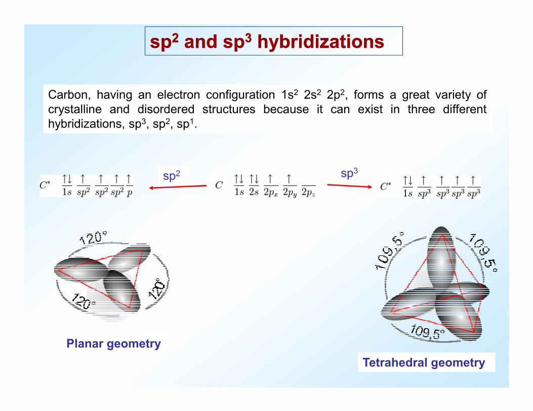
spsp22 and spand sp33 hybridizationshybridizations
sp3sp2
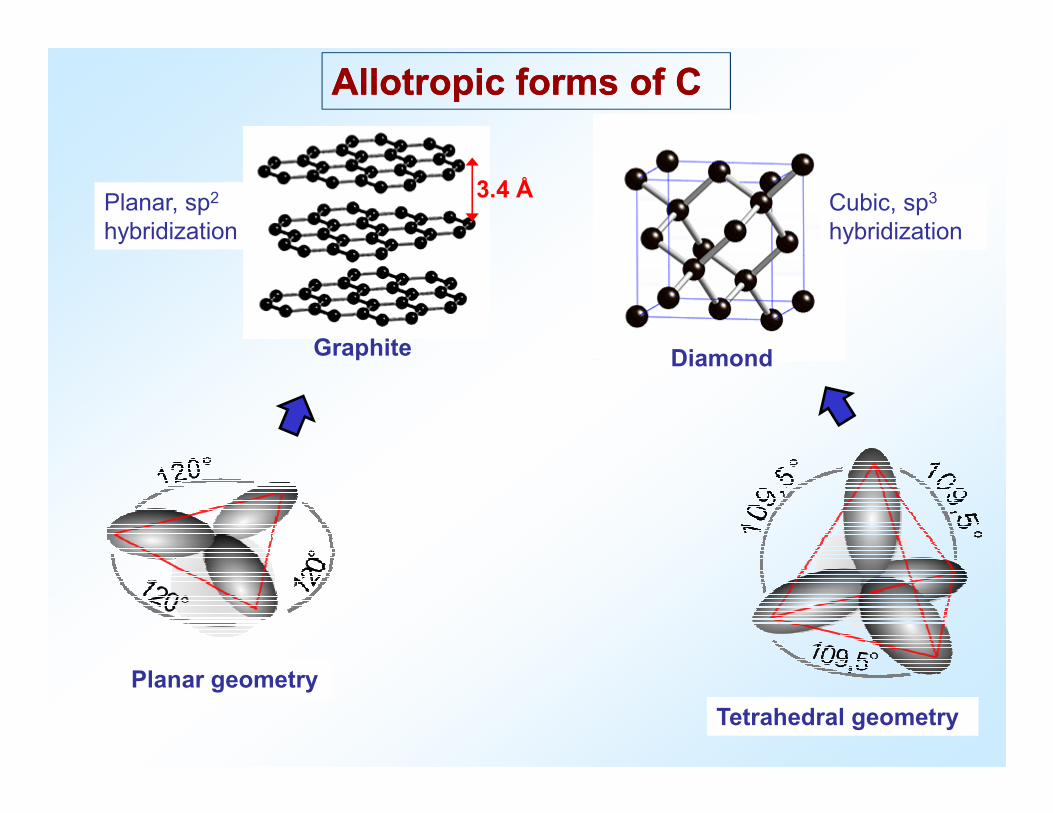
Carbon, having an electron configuration 1s2 2s2 2p2, forms a great variety ofcrystalline and disordered structures because it can exist in three differenthybridizations, sp3, sp2, sp1.
Planar geometry
Tetrahedral geometry
Cubic, sp3
hybridization
Diamond
3.4 ÅPlanar, sp2
hybridization
Graphite
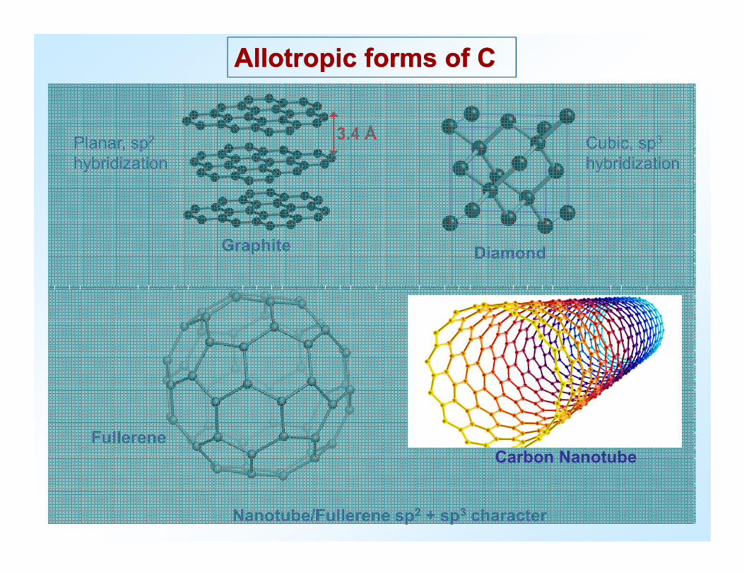
Allotropic forms of CAllotropic forms of C
Planar geometry
Tetrahedral geometry

Allotropic forms of CAllotropic forms of C
Cubic, sp3
hybridization
Diamond
3.4 ÅPlanar, sp2
hybridization
Graphite
Nanotube
Fullerene
Nanotube/Fullerene sp2 + sp3 character
Physical and chemical properties are a direct consequence of the carbon-carbon bonds and lattice configuration

Allotropic forms of CAllotropic forms of C
Cubic, sp3
hybridization
Diamond
3.4 ÅPlanar, sp2
hybridization
GraphiteGraphene
Nanotube/Fullerene sp2 + sp3 character
Carbon NanotubeFullerene

Allotropic forms of CAllotropic forms of C
Cubic, sp3
hybridization
Diamond
3.4 ÅPlanar, sp2
hybridization
GraphiteGraphene
Nanotube/Fullerene sp2 + sp3 character
Carbon NanotubeFullerene

Discovery of fullerene or buckyballDiscovery of fullerene or buckyball
H. W. Kroto, J. R. Heath, S. C. O’Brien, R. F. Curl and R. E. Smalley, Nature 318 (1985) 162–63.
Discovery of fullereneDiscovery of fullerene
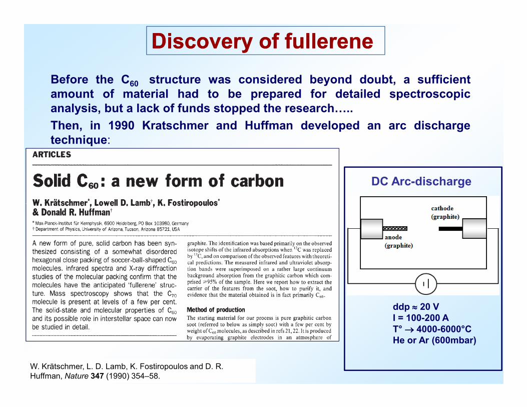
Before the C60 structure was considered beyond doubt, a sufficientamount of material had to be prepared for detailed spectroscopicanalysis, but a lack of funds stopped the research6..
Then, in 1990 Kratschmer and Huffman developed an arc dischargetechnique:
DC Arc-discharge
W. Krätschmer, L. D. Lamb, K. Fostiropoulos and D. R. Huffman, Nature 347 (1990) 354–58.
ddp ≈≈≈≈ 20 VI = 100-200 AT° →→→→ 4000-6000°CHe or Ar (600mbar)

Characterization of fullereneCharacterization of fullerene
MS
XRD
W. Krätschmer, L. D. Lamb, K. Fostiropoulos and D. R. Huffman, Nature 347 (1990) 354–58.
UV-VisFT-IR

FullerenesFullerenes
C540
C960
C240
C
8.34 Å ; 7.66 Å
Different fullerenes can be separated
C60 (bucky ball)
d= 7.1 Å
C70 (rugby-ball shaped)Different fullerenes can be separated by means of chromatographic
column.

Fullerene propertiesFullerene properties
� Fullerenes are non-toxic and are soluble in several organic solvents.
�Fullerenes are quite stable. However the spherical curvature producesangle strain that allows fullerenes to undergo characteristic reactions ofaddition to double bonds (hybridization turns from sp2 to sp3).
�C60 in organic solvents exhibits 5 stages of reversible oxidation/reduction,hence fullerene can work either as electrophiles or nucleophiles.
CHEMICAL REACTIVITY
hence fullerene can work either as electrophiles or nucleophiles.
C60F18
Image created by Chris Ewels, www.ewels.info

Fullerene propertiesFullerene properties
Fullerenes, packed in fcc structure, can be intercalated with alkali andalkaline-earth metal atoms which provide electrons to the conductionband (from semi-conducting to metallic behavior). In 1991 potassium-doped fullerene (K3C60) revealed superconducting behavior at 18K.
DERIVATIVES: EXOHEDRAL, ENDOHEDRAL and ON-SITE DOPING
L. Forrò and L. Mihaly, Rep. Prog. Phys. 64 (2001) 649-699.

Fullerene propertiesFullerene properties
DERIVATIVES: EXOHEDRAL, ENDOHEDRAL and ON-SITE DOPING
� In the endohedral doping a foreign atom is inserted in the inner cavity(M @ C60). This doping can be performed either by ion implantation orcoevaporation of C and metal in arc discharge system.
� The on-site doping is achieved by replacing one carbon atom with anitrogen atom ((C59N)2 azafullerene).
CNTs !!!
Image created by Chris Ewels, www.ewels.info L. Forrò and L. Mihaly, Rep. Prog. Phys. 64 (2001) 649-699.

Fullerenes applicationsFullerenes applications
� Hydrogen or oxygen storage: hydrogenation of fullerene produceshydrides. The reaction is reversible and can be catalyzed with metals (lowpressure).
� Catalyst: fullerene promotes the conversion of methane into higherhydrocarbons and inhibits coking reactions.
� Sensor: fullerene based capacitors can be used to detect ppm of H2S� Sensor: fullerene based capacitors can be used to detect ppm of H2Sin N2, ppm of water in isopropanol.
� Diamond precursor: fullerene can be transformed to diamond at highpressure (RT) or can be used as a diamond nucleation center during CVD.
� Alloy strengthening/hardening (Ti), improvement of electricalconductivity of Cu alloys.
� Biomedical field: inhibition of human HIV replication and HIV-1protease. Biological antioxidant (radical sponge).
Allotropic forms of CAllotropic forms of C
Cubic, sp3
hybridization
Diamond
3.4 ÅPlanar, sp2
hybridization
Graphite
Nanotube/Fullerene sp2 + sp3 character
FullereneCarbon Nanotube

Discovery of CNTsDiscovery of CNTs
Many scientific papers start citing ‘‘the discovery of Many scientific papers start citing ‘‘the discovery of carbon nanotubes by Iijima in 1991. . .’’carbon nanotubes by Iijima in 1991. . .’’
Arc-discharge: from endohedral fullerene to CNTs
S. Iijima, Nature 354, (1991) 56
Discovery of CNTsDiscovery of CNTs
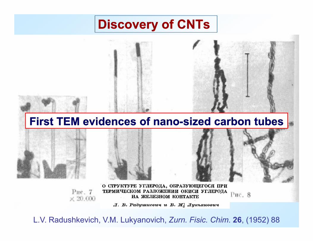
First TEM evidences of nanoFirst TEM evidences of nano--sized carbon tubessized carbon tubes
L.V. Radushkevich, V.M. Lukyanovich, Zurn. Fisic. Chim. 26, (1952) 88
First TEM evidences of nanoFirst TEM evidences of nano--sized carbon tubessized carbon tubes

Discovery of CNTsDiscovery of CNTs

What are CNTs?What are CNTs?
Rolled graphene sheet
Diameter: 0,7 - 100 nm
Length: from few tens of nm up to several mm
EvenEven ifif thethe curvaturecurvature causescauses aa higherhigher strainstrain energy,energy, aa defectdefect freefree CNTCNThashas anan overalloverall lowerlower energyenergy statestate thanthan graphitegraphite becausebecause danglingdanglingbondsbonds areare removedremoved.. ThisThis explainsexplains highhigh thermalthermal stabilitystability andand chemicalchemicalinertnessinertness..

CNTs classificationCNTs classification
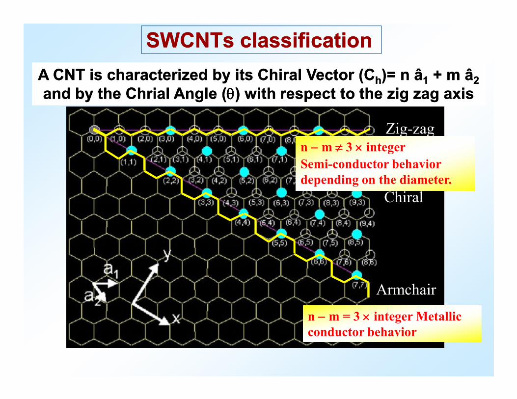
SWCNTs classificationSWCNTs classification
Zig-zag
Chiral
n −−−− m ≠≠≠≠ 3 ×××× integer
Semi-conductor behavior
depending on the diameter.
A CNT is characterized by its Chiral Vector (A CNT is characterized by its Chiral Vector (CChh))= = n n ââ11 + + m m ââ22
and by the Chrial Angle (and by the Chrial Angle (θθθθθθθθ) with respect to the zig zag axis) with respect to the zig zag axis
Armchair
Chiral
n −−−− m = 3 ×××× integer Metallic
conductor behavior

Armchair (5,5)
θθθθ = 30°°°°
Zig Zag (9,0)
θθθθ = 0°°°°
SWCNTs classificationSWCNTs classification
θθθθ = 0°°°°
Chiral (10,5)
0°°°° θθθθ < 30°

CharacterizationCharacterizationHR-TEMSEM
200 400 600 800
0
20
40
60
80
100
Weight derivative [%/°C]
Temperature [°C]
-0.2
0.0
0.2
0.4
0.6
0.8
1.0
1.2
1.4
1.6
Air 20°C/min
Weight [%
]
TGA
Temperature [°C]
10 20 30 40 50 60 70 80 90 100
(*)
(004)
(100)
(*)
(002)
Intensity (arb.unit)
2θ (°)
XRD
500 1000 1500 20000
200
400
600
800
1000
1200
1400
1600
1800
Raman shift (cm-1)
Intensity (a.u.)
Raman spectroscopy
1344 cm-1
D peak
1591 cm-1
G peak
RBM

Properties of defect free CNTsProperties of defect free CNTs
Young’s modulus
(GPa)
Tensile Strength
(GPa)
Density
(g/cm3)
MWCNT 1200 ∼150 2.6
SWCNT 1054 75 1.3
SWCNT bundle 563 ∼150 1.3
Graphite (in-plane) 350 2.5 2.2-2.6
Steel 208 0.4 7.8
Thermal conductivity Electrical conductivityThermal conductivity
(W/mK) RT
Electrical conductivity
(A/cm2)
MWCNT ∼3000 ≤109
SWCNT ∼6000 Depends on the chirality
SWCNT bundle ∼3000 ≤109
Graphite (in-plane) ∼1700 ≤109
Diamond 2000 - 2500
Copper 401 106

FunctionalizationFunctionalization
Chemical functionalization can be used to tune CNTs properties.
� Composite – improving compatibility matrix/filler
� Biomedical – improving biocompatibility, drug delivery, diagnosis6
Chemical (KMnO4, HNO3-H2SO4) or plasma oxidation change surface properties while producing lattice defects (removable by annealing).
Van der Waals interactions with porphyrin or pyrene derivatives are less effective.

CNT properties/applicationsCNT properties/applications

CNT synthesisCNT synthesis
High temperature methods
� Arc Discharge
� Laser ablation
These techniques generate small amount of high quality CNTs by sublimation ofgraphite in presence of catalyst particles.
Gas phase (vapor phase) methods
� Chemical Vapor Deposition (CVD) and plasma enhanced-CVD (PECVD)
During CVD a conventional heat source is used to form CNTs by thermal cracking ofhydrocarbons. A plasma source is used in PE-CVD to create a glow discharge whichprovokes a low temperature precursor dissociation
Nanoparticles of Co, Ni or Fe are necessary to catalyze the growth

CNT synthesisCNT synthesis
Gas or low bp liquids can be
used. The CVD technique is
simple, low-cost, easily scalable
for commercial production and
allows to produce large amounts
of CNTs with high purity.
CVD
PECVD
V= -600VT° →→→→ 400-800°CAr or N2 (0.1-30 Torr)
Plasma discharge sources:
- direct current (DC),
- alternating current (AC),
- radio frequency (RF),
- hot-filament aided with DC,
- microwaves

We do like gas phase techniquesWe do like gas phase techniques
CVD allows to produce cm long CNTs. With direct spinning is also possible thesynthesis of very long CNT ropes in situ.
Ya-Li Li et al., Science 304 (2004) 276 S. Musso et al. Carbon 45 (2007) 1133-1136

CNT growth mechanismCNT growth mechanismTwo theories for the carbon-metal interaction:
� Dissolution and saturation of carbon atoms in metal nanoparticles andprecipitation of carbon.
� The catalyst provokes dehydroaromatization (DHA) of cyclic molecules ofhydrocarbon.
Base growth mechanism is dueto a strong adhesion of thecatalyst to the substrate.
Tip growth mechanism is due to aweak adhesion of the catalyst tothe substrate.

Tip growth mechanismTip growth mechanism
Stephan Hofmann et al., Nanoletters 7 (2007) 602

TOXICITYTOXICITY
Small CNT
Factors influencing the safety of CNTs in vivo.
Big CNT

Allotropic forms of CAllotropic forms of C
Cubic, sp3
hybridization
Diamond
3.4 ÅPlanar, sp2
hybridization
GraphiteGraphene
Nanotube/Fullerene sp2 + sp3 character
Carbon NanotubeFullerene

Allotropic forms of CAllotropic forms of C
GraphiteGraphene
Nanotube Fullerene
� Graphene was largely studied from a theoretical point of view.
� The unsuccessful attempts to synthesize it seemed to confirm the theory that truly two-dimensional crystals (any kind of crystal) could not exist.
� In 2-D the thermal vibration of the atoms should lead to a displacementcomparable to interatomic distance (thermodynamically unstable).
� The very large perimeter-to-surface ratio of 2-D crystals promotes a collapse.

Discovery of Graphene?... Not yet6Discovery of Graphene?... Not yet6
Epitaxial Growth by CVD
Graphene and few layers of graphene are grown on Ni
Graphene is not free-standing and its properties are strongly affected bysubstrate:� Significant charge transfer from the substrate to the epitaxial graphene
� Hybridization between the d orbitals of the substrate atoms and π orbitals ofgraphene, which significantly alters the electronic structure of the epitaxialgraphene.

Discovery of GrapheneDiscovery of Graphene
K.S. Novoselov et al., Science 306 (2004) 666-669
Free-standing graphene films (10 µµµµm in size) were
prepared by mechanical exfoliation (repeated peeling) of
small mesas of highly oriented pyrolytic graphite (HOPG).
MultiMulti--layers graphenelayers graphene
� The electronic structure of graphene rapidly evolves with the number oflayers, approaching the 3D limit of graphite at 10 layers.
� Only graphene and its bi-layer has simple electronic spectra: they are bothzero-gap semiconductors (or zero-overlap semimetals).
� For three or more layers, the spectra become more complicated, severalcharge carriers appear, and the conduction and valence bands start notably
J.C. Meyer et al., Nature 446 (2007) 60-63
charge carriers appear, and the conduction and valence bands start notablyoverlapping. This allows single-, double and few (3 to <10) layer graphene to bedistinguished as three different types of 2D crystals (‘graphenes’).
� Thicker structures should be considered as thin films of graphite.

CharacterizationCharacterization
HR-TEM
500 nm
2 nm
J.C. Meyer et al., Nature 446 (2007) 60-631 nm
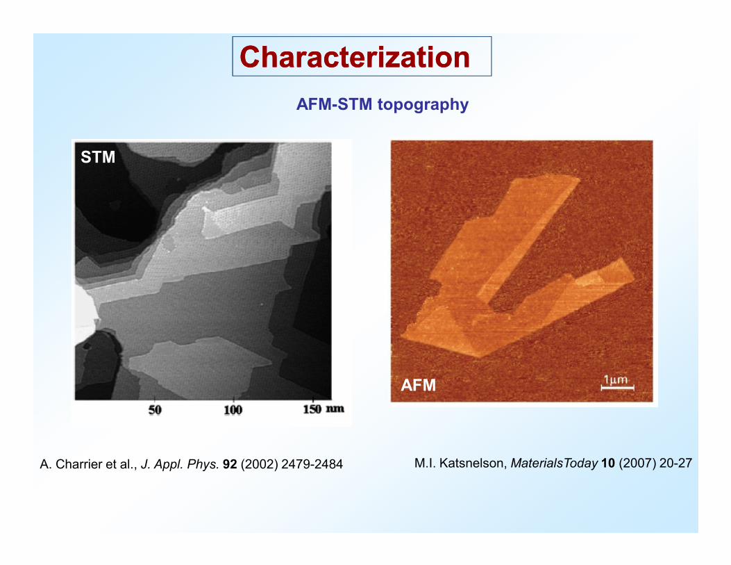
CharacterizationCharacterization
AFM-STM topography
STM
M.I. Katsnelson, MaterialsToday 10 (2007) 20-27A. Charrier et al., J. Appl. Phys. 92 (2002) 2479-2484
AFM

CharacterizationCharacterization
Nanobeam e-diffraction
J.C. Meyer et al., Nature 446 (2007) 60-63
Since graphene is microscopically corrugated the e-diffraction peaks of graphene become broader whileincreasing the tilt angle.
The elastic strain can intrinsically provide thethermodynamic stability of the film.
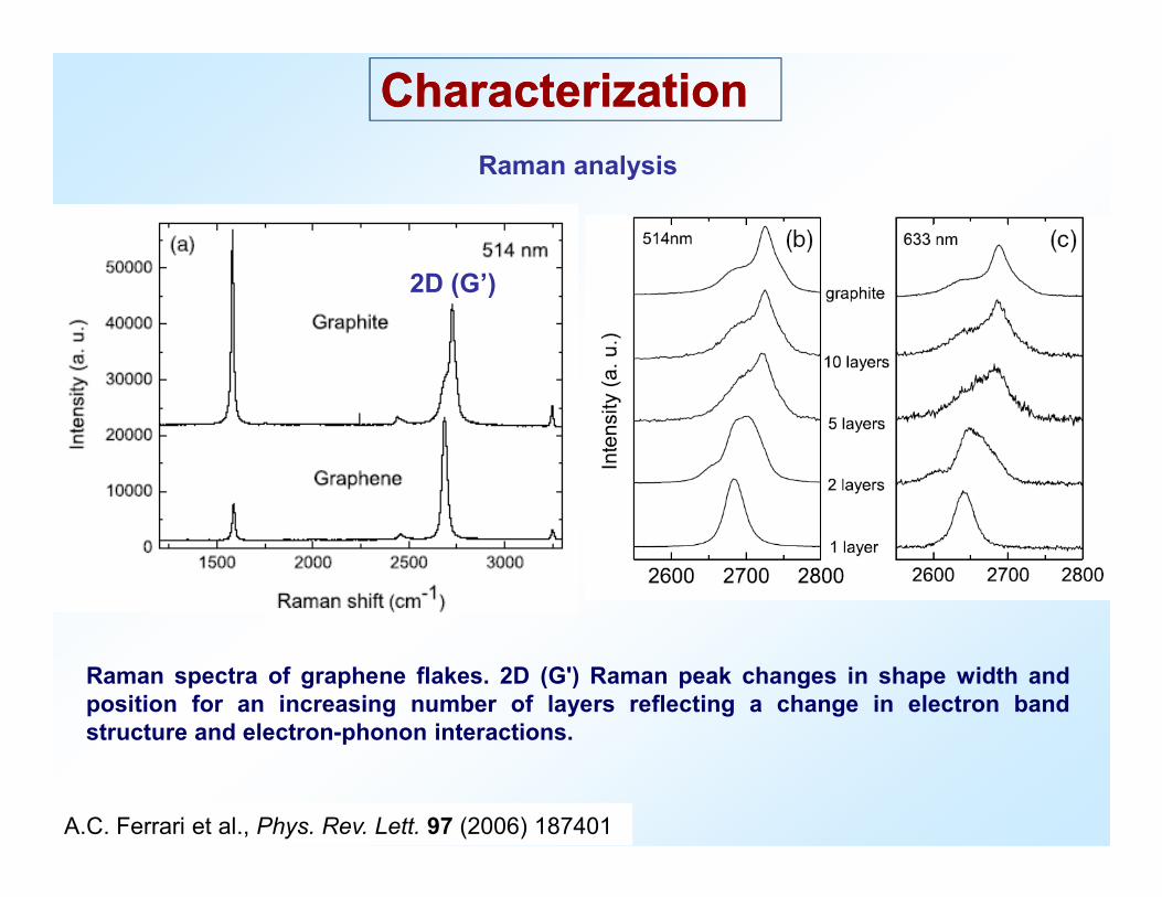
CharacterizationCharacterization
2D (G’)
Raman analysis
Raman spectra of graphene flakes. 2D (G') Raman peak changes in shape width andposition for an increasing number of layers reflecting a change in electron bandstructure and electron-phonon interactions.
A.C. Ferrari et al., Phys. Rev. Lett. 97 (2006) 187401

CharacterizationCharacterization
Confocal Raman
Confocal Raman map (2D band center of mass position).1, 2, 3 and 4- layered flakes can be easily distinguishedwhen using a color palette scale.
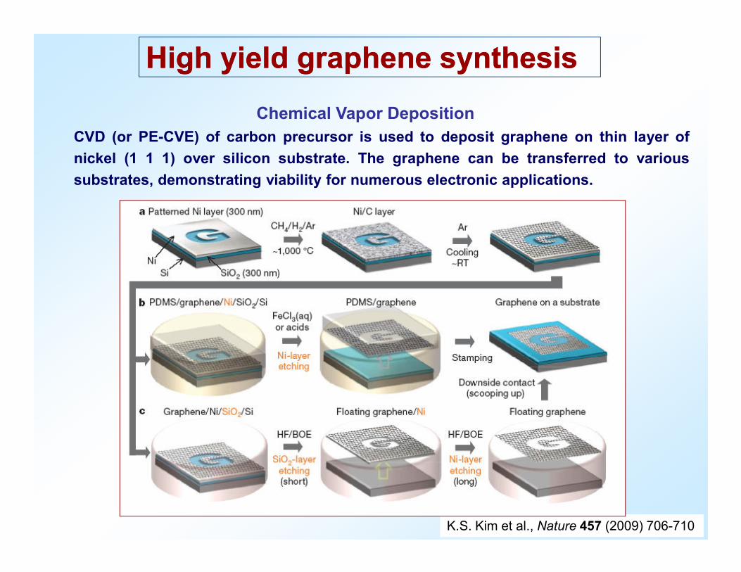
Chemical Vapor Deposition
High yield graphene synthesisHigh yield graphene synthesis
CVD (or PE-CVE) of carbon precursor is used to deposit graphene on thin layer of
nickel (1 1 1) over silicon substrate. The graphene can be transferred to various
substrates, demonstrating viability for numerous electronic applications.
K.S. Kim et al., Nature 457 (2009) 706-710

Other graphene synthesisOther graphene synthesis
Hydrazine reduction
� Silicon carbide (6H-SiC) is heated between 1080 and 1320°C giving the
growth of graphene. The face of the SiC used for graphene creation, Si-
terminated or C-terminated, highly influences the thickness, mobility and
carrier density of the graphene.
Silicon carbide sublimation
� Graphene oxide paper is reduced to single-layer graphene in a solution of pure hydrazine (NH2-NH2).
� Gram-quantities of graphene are produced by the reduction of ethanol bysodium metal, followed by pyrolysis of the ethoxide product, and washingwith water to remove sodium salts.
Sodium reduction of ethanol
Unfolding CNTs
� Graphene ribbons are produced by cutting and unfolding CNTs viachemical etching (KMnO4-H2SO4) o plasma etching.

Graphene properties/applicationsGraphene properties/applications
Charge carriers (electrons and holes) have high density (1013 cm-2) and highmobility (15000 cm2V-1s-1) at RT, and the mobility weakly depends ontemperature (only impurity scattering):
� Ballistic field effect transistor (high speed electronic devices)
Electrical properties
K.S. Novoselov et al., Science 306 (2004) 666-669
Rather modest on-off conductance ratio of ~30 at RT

Graphene properties/applicationsGraphene properties/applications
The transistor conductance can be significantly altered (106 on-off ratio at RT)by a reversible chemical modification. In presence of humidity the electric fieldchanges the graphene to graphane (hydrogenated derivative, 3.5 eV of bandgap) and graphene oxide (-OH, insulator).
� Non volatile memory application.
Electrical properties
T.J. Echtermeyer et al., IEEE Electronic Device Letters 29 (2008) 952

Graphene properties/applicationsGraphene properties/applications
Graphene chip can double the frequency of an electromagnetic signal.
� Graphene chips can transmit data faster than standard silicon chips,consuming less energy and having a higher S/N ratio.
Graphene has high electrical conductivity, high optical transparency, mechanicalstrength and flexibility.
� Touchscreens, liquid crystal displays, organic photovoltaic cells,
Electrical properties
Touchscreens, liquid crystal displays, organic photovoltaic cells,stretchable electrodes.
K.S. Kim et al., Nature 457 (2009) 706-710

Graphene properties/applicationsGraphene properties/applications
Graphene has an incredibly high surface area to mass ratio.
� Ultra-capacitors with great energy storage density.
Graphene has electrical conductivity can be tuned by gas molecule absorption.
� High sensitive gas sensors.
Graphene stripes, called graphene nanoribbons (GNRs), have electrical
Electrical properties
Graphene stripes, called graphene nanoribbons (GNRs), have electricalproperties that depends on the un-bonded edges.
� Armchair GNRs are semiconductors with a band gap that increases withthe decreasing of the width.
� Research is being done to create quantum dots by changing the width ofGNRs at select points along the ribbon, creating quantum confinement.

Graphene properties/applicationsGraphene properties/applications
High thermal conductivity (~ 5000 Wm-1K-1)
� Heat sinks.
Graphenen is very strong (Young’s modulus 0.5 TPa) and stiff (elastic constant1-5N/m).
� NEMS applications as pressure sensors or resonators.� NEMS applications as pressure sensors or resonators.
� Nanocomposites
Small spin-orbit interaction and near absence of nuclear magnetic moments incarbon. GNRs in the zig-zag orientation, at low temperatures, show spin-polarized edge currents.
� Spintronics (magnetoelectronics) applications

Graphene properties/applicationsGraphene properties/applications
Graphene oxide is obtained by oxidizing (KMnO4-H2SO4) and chemicallyprocessing graphite/graphene. The graphene oxide flakes dispersed in watercan give well-ordered structure with exceptional mechanical properties.
� Nanocomposites
H. Chen et al., Adv. Mater. 20 (2008) 3557-3561
S. Stankovich et al., J. Mater. Chem. 16 (2006) 155

Thank you for your Thank you for your attention!attention!