
Graphene FETs with Low-Resistance Hybrid Contacts … Article Graphene FETs with Low-Resistance...
11
nanomaterials Article Graphene FETs with Low-Resistance Hybrid Contacts for Improved High Frequency Performance Chowdhury Al-Amin *, Mustafa Karabiyik, Phani Kiran Vabbina, Raju Sinha and Nezih Pala Department of Electrical and Computer Engineering, Florida International University, Miami, FL 33174, USA; mkara006@fiu.edu (M.K.);pvabb001@fiu.edu (P.K.V.); rsinh001@fiu.edu (R.S.); npala@fiu.edu (N.P.) * Correspondence: calam003@fiu.edu; Tel.: +1-305-348-3713 Academic Editors: Ho Won Jang and Soo Young Kim Received: 16 February 2016; Accepted: 3 May 2016; Published: 10 May 2016 Abstract: This work proposes a novel geometry field effect transistor with graphene as a channel—graphene field-effect transistor (GFET), having a hybrid contact that consists of an ohmic source/drain and its extended part towards the gate, which is capacitively coupled to the channel. The ohmic contacts are used for direct current (DC) biasing, whereas their capacitive extension reduces access region length and provides the radio frequency (RF) signal a low impedance path. Minimization of the access region length, along with the paralleling of ohmic contact’s resistance and resistive part of capacitively coupled contact’s impedance, lower the overall source/drain resistance, which results in an increase in current gain cut-off frequency, f T . The DC and high-frequency characteristics of the two chosen conventional baseline GFETs, and their modified versions with proposed hybrid contacts, have been extensively studied, compared, and analyzed using numerical and analytical techniques. Keywords: graphene field-effect transistor (GFET); current-gain cut-off frequency; access resistance; capacitive coupling; radio frequency 1. Introduction Graphene is a promising two-dimensional material exhibiting exceptionally high crystal and electronic qualities, which has fascinated researchers for decades. The richness of its electronic and optical properties include, but are not limited to, its high residual carrier concentration, mobility, Fermi velocity, high thermal conductivity, its perfect 2D body, optical transparency, and high mechanical stability [1–5], which have already revealed a cornucopia of potential engineering and application. Numerous research groups have seen graphene as a descendant of Silicon for analog devices, though the roadblock of graphene—its zero bandgap [6]—made it incapable of switching off field effect transistors (FETs) and, thus, inappropriate for logic devices. An important metric for a radio frequency transistor’s performance measurement is its current gain cutoff frequency, f T . The cutoff frequency inversely depends on source/drain resistance, which is composed of contact resistance and access resistance, and their minimization ensures f T increment. The detrimental effect of access resistance on a graphene FET is much more prominent compared to that on other FETs. In addition to that, handing this access resistance in graphene field-effect transistors (GFETs) is much more challenging compared to other FETs. That is the reason why access resistance is getting a great deal of attention in GFETs, which prompted us to work on a viable way to reduce it. For example, the typical access resistance of silicon metal oxide field effect transistor (Si-MOSFET) is ~150 ohm-um [7], on the other hand, this quantity, for GFETs, is ~350 ohm-um and is 80% of the total device resistance [8]. In addition to this, in Si-MOSFET, the access region is highly doped by ion implantation in order to reduce access resistance [9], whereas, this type of high energy doping scheme is not viable for GFETs, where single or a few layer graphene form the device’s access Nanomaterials 2016, 6, 86; doi:10.3390/nano6050086 www.mdpi.com/journal/nanomaterials
Transcript of Graphene FETs with Low-Resistance Hybrid Contacts … Article Graphene FETs with Low-Resistance...

nanomaterials
Article
Graphene FETs with Low-Resistance Hybrid Contactsfor Improved High Frequency Performance
Chowdhury Al-Amin *, Mustafa Karabiyik, Phani Kiran Vabbina, Raju Sinha and Nezih Pala
Department of Electrical and Computer Engineering, Florida International University, Miami, FL 33174, USA;[email protected] (M.K.); [email protected] (P.K.V.); [email protected] (R.S.); [email protected] (N.P.)* Correspondence: [email protected]; Tel.: +1-305-348-3713
Academic Editors: Ho Won Jang and Soo Young KimReceived: 16 February 2016; Accepted: 3 May 2016; Published: 10 May 2016
Abstract: This work proposes a novel geometry field effect transistor with graphene as achannel—graphene field-effect transistor (GFET), having a hybrid contact that consists of an ohmicsource/drain and its extended part towards the gate, which is capacitively coupled to the channel.The ohmic contacts are used for direct current (DC) biasing, whereas their capacitive extensionreduces access region length and provides the radio frequency (RF) signal a low impedance path.Minimization of the access region length, along with the paralleling of ohmic contact’s resistance andresistive part of capacitively coupled contact’s impedance, lower the overall source/drain resistance,which results in an increase in current gain cut-off frequency, fT. The DC and high-frequencycharacteristics of the two chosen conventional baseline GFETs, and their modified versions withproposed hybrid contacts, have been extensively studied, compared, and analyzed using numericaland analytical techniques.
Keywords: graphene field-effect transistor (GFET); current-gain cut-off frequency; access resistance;capacitive coupling; radio frequency
1. Introduction
Graphene is a promising two-dimensional material exhibiting exceptionally high crystal andelectronic qualities, which has fascinated researchers for decades. The richness of its electronic andoptical properties include, but are not limited to, its high residual carrier concentration, mobility, Fermivelocity, high thermal conductivity, its perfect 2D body, optical transparency, and high mechanicalstability [1–5], which have already revealed a cornucopia of potential engineering and application.Numerous research groups have seen graphene as a descendant of Silicon for analog devices, thoughthe roadblock of graphene—its zero bandgap [6]—made it incapable of switching off field effecttransistors (FETs) and, thus, inappropriate for logic devices.
An important metric for a radio frequency transistor’s performance measurement is its currentgain cutoff frequency, fT. The cutoff frequency inversely depends on source/drain resistance, which iscomposed of contact resistance and access resistance, and their minimization ensures fT increment.The detrimental effect of access resistance on a graphene FET is much more prominent comparedto that on other FETs. In addition to that, handing this access resistance in graphene field-effecttransistors (GFETs) is much more challenging compared to other FETs. That is the reason why accessresistance is getting a great deal of attention in GFETs, which prompted us to work on a viable wayto reduce it. For example, the typical access resistance of silicon metal oxide field effect transistor(Si-MOSFET) is ~150 ohm-um [7], on the other hand, this quantity, for GFETs, is ~350 ohm-um and is80% of the total device resistance [8]. In addition to this, in Si-MOSFET, the access region is highlydoped by ion implantation in order to reduce access resistance [9], whereas, this type of high energydoping scheme is not viable for GFETs, where single or a few layer graphene form the device’s access
Nanomaterials 2016, 6, 86; doi:10.3390/nano6050086 www.mdpi.com/journal/nanomaterials
Nanomaterials 2016, 6, 86 2 of 11
region. Techniques to reduce GFET contact resistance have been proposed and reported by numerousgroups [10–15]. Reduction of access resistance for enhanced performance in graphene FETs [16–20], inIII-N high electron mobility transistors (HEMTs) [21], and in GaAs/AlGaAs HEMTs [22], have alsobeen reported. In this work, we have proposed, studied, and extensively analyzed a GFET with hybridcontacts capable of simultaneously reducing the access resistance and contact resistance of the device.The capacitive coupled part of the contact reduces the contact resistance and provides a low resistancepath for the high frequency signal. In addition, the extension towards the gate reduces the access regionlength and the associated resistance—the access resistance. The approaching capacitive extensiontowards the gate might introduce additional parasitic capacitance; however, the cumulative aidingeffect of contact and access resistance reduction on high frequency performance is more significantand prominent than the detrimental effect of additional parasitic capacitances. The elimination of theaccess region by using a sophisticated fabrication method, e.g., a self-aligned process, could be a betterway to handle access resistance; however, the proposed method offers a promising viable alternative,where complex/sophisticated lithographic techniques with smaller tolerances need to be avoided.
2. Theory
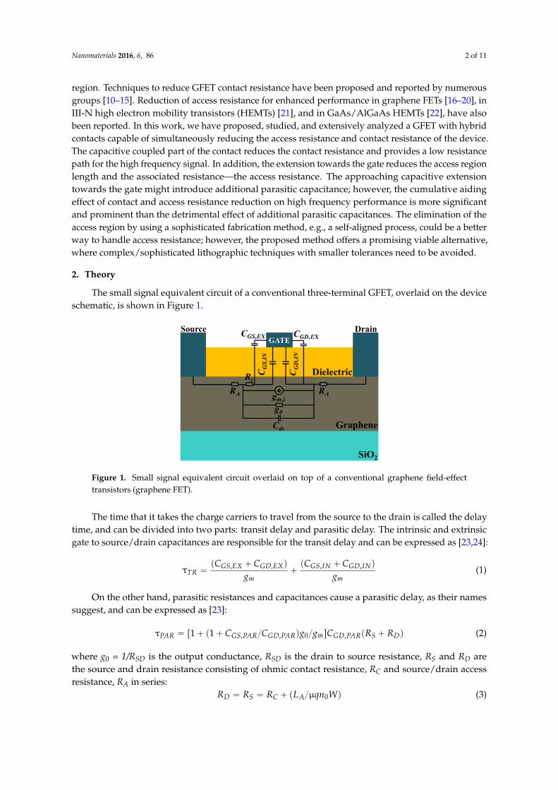
The small signal equivalent circuit of a conventional three-terminal GFET, overlaid on the deviceschematic, is shown in Figure 1.
Nanomaterials 2016, 6, 86 2 of 10
Techniques to reduce GFET contact resistance have been proposed and reported by numerous groups
[10–15]. Reduction of access resistance for enhanced performance in graphene FETs [16–20], in III-N
high electron mobility transistors (HEMTs) [21], and in GaAs/AlGaAs HEMTs [22], have also been
reported. In this work, we have proposed, studied, and extensively analyzed a GFET with hybrid
contacts capable of simultaneously reducing the access resistance and contact resistance of the device.
The capacitive coupled part of the contact reduces the contact resistance and provides a low resistance
path for the high frequency signal. In addition, the extension towards the gate reduces the access
region length and the associated resistance—the access resistance. The approaching capacitive
extension towards the gate might introduce additional parasitic capacitance; however, the
cumulative aiding effect of contact and access resistance reduction on high frequency performance is
more significant and prominent than the detrimental effect of additional parasitic capacitances. The
elimination of the access region by using a sophisticated fabrication method, e.g., a self-aligned
process, could be a better way to handle access resistance; however, the proposed method offers a
promising viable alternative, where complex/sophisticated lithographic techniques with smaller
tolerances need to be avoided.
2. Theory
The small signal equivalent circuit of a conventional three-terminal GFET, overlaid on the device
schematic, is shown in Figure 1.
Figure 1. Small signal equivalent circuit overlaid on top of a conventional graphene field-effect
transistors (graphene FET).
The time that it takes the charge carriers to travel from the source to the drain is called the delay
time, and can be divided into two parts: transit delay and parasitic delay. The intrinsic and extrinsic
gate to source/drain capacitances are responsible for the transit delay and can be expressed as [23,24]:
, , , ,( ) ( )τ
GS EX GD EX GS IN GD IN
TR
m m
C C C C
g g
(1)
On the other hand, parasitic resistances and capacitances cause a parasitic delay, as their names
suggest, and can be expressed as [23]:
,, , 0τ [1 (1 ( )/ ) / ]PAR GS PAR GD P GDAR PAm R S DC C g g C R R (2)
where g0 = 1/RSD is the output conductance, RSD is the drain to source resistance, RS and RD are the
source and drain resistance consisting of ohmic contact resistance, RC and source/drain access
resistance, RA in series:
0( /μ )D S C AR R R L qn W (3)
where LA is the access region length (LGS and LGD), μ is the carrier mobility, q is electronic charge, n0 is
the residual carrier density in graphene, and W is the device width. For simplicity, the effects of
Figure 1. Small signal equivalent circuit overlaid on top of a conventional graphene field-effecttransistors (graphene FET).
The time that it takes the charge carriers to travel from the source to the drain is called the delaytime, and can be divided into two parts: transit delay and parasitic delay. The intrinsic and extrinsicgate to source/drain capacitances are responsible for the transit delay and can be expressed as [23,24]:
τTR “pCGS,EX ` CGD,EXq
gm`pCGS,IN ` CGD,INq
gm(1)
On the other hand, parasitic resistances and capacitances cause a parasitic delay, as their namessuggest, and can be expressed as [23]:
τPAR “ r1` p1` CGS,PARCGD,PARqg0gmsCGD,PARpRS ` RDq (2)
where g0 = 1/RSD is the output conductance, RSD is the drain to source resistance, RS and RD arethe source and drain resistance consisting of ohmic contact resistance, RC and source/drain accessresistance, RA in series:
RD “ RS “ RC ` pLAµqn0Wq (3)

Nanomaterials 2016, 6, 86 3 of 11
where LA is the access region length (LGS and LGD), µ is the carrier mobility, q is electronic charge,n0 is the residual carrier density in graphene, and W is the device width. For simplicity, the effectsof graphene doping, due to contacts and the gradient in carriers of the access region, have not beenincluded; however, the effect is well explained in Reference [25]. In a common emitter configuration,the input terminal of a FET is the gate and the output terminal is the drain. As it is a FET, the inputcurrent in direct current (DC) is zero. As a result, the current gain for DC is theoretically infinite,h21 = iout/iin = iout/0 = 8. The reactance of gate to channel capacitance is inversely dependent onfrequency, and with increasing frequency, the reactance decreases. As a result, the input alternatingcurrent (AC) current also increases with frequency, which results in a decrease of current gain. Thefrequency at which, current gain drops to unity is called the current gain cut-off frequency, and can berelated to the total delay time in the device, as follows:
12π fT “ τTR ` τPAR (4)
After substituting Equations (1) and (2) into Equation (4) and rearranging, the current gain cut-offfrequency, fT of the GFET can be related to the small signal equivalent circuit parameters, as follows:
fT “gm p2πq
rCGS ` CGDs ˆ r1` pRS ` RDqRSDs ` CGD ˆ gm ˆ pRS ` RDq(5)
where, RSD is the total channel resistance.If two capacitively coupled contacts (C3s) are placed on the access regions and connected to the
ohmic source/drain, as shown in Figure 2, C3 will make a path for high frequency RF signal parallelto the ohmic contact. The C3 impedance, ZC3 = RC3´jXC3, consists of real and imaginary parts, andthe total contact impedance comes to be ZC = RC||ZC3 = RC||(RC3´jXC3). After rearrangement andsimplification, ZC can be expressed as:
ZC “R2
CRC3 ` R2C3RC ` X2
C3RC
pRC ` RC3q2` X2
C3
´ jXC3R2
C
pRC ` RC3q2` X2
C3
“ R1C ´ jX1C (6)
Nanomaterials 2016, 6, 86 3 of 10
graphene doping, due to contacts and the gradient in carriers of the access region, have not been
included; however, the effect is well explained in Reference [25]. In a common emitter configuration,
the input terminal of a FET is the gate and the output terminal is the drain. As it is a FET, the input
current in direct current (DC) is zero. As a result, the current gain for DC is theoretically infinite, h21
= iout/iin = iout/0 = . The reactance of gate to channel capacitance is inversely dependent on frequency,
and with increasing frequency, the reactance decreases. As a result, the input alternating current (AC)
current also increases with frequency, which results in a decrease of current gain. The frequency at
which, current gain drops to unity is called the current gain cut-off frequency, and can be related to
the total delay time in the device, as follows:
1/ 2π τ τTRT PARf (4)
After substituting Equations (1) and (2) into Equation (4) and rearranging, the current gain cut-
off frequency, fT of the GFET can be related to the small signal equivalent circuit parameters, as
follows:
/ 2π
[ ] 1 ( ) /
m
T
GS GD S D SD GD m S D
gf
C C R R R C g R R
(5)
where, RSD is the total channel resistance.
If two capacitively coupled contacts (C3s) are placed on the access regions and connected to the
ohmic source/drain, as shown in Figure 2, C3 will make a path for high frequency RF signal parallel
to the ohmic contact. The C3 impedance, ZC3 = RC3−jXC3, consists of real and imaginary parts, and the
total contact impedance comes to be ZC = RC||ZC3 = RC||(RC3−jXC3). After rearrangement and
simplification, ZC can be expressed as:
2 2 22
3 3 3
2 2 2
3 3
3
2
3 3( ( ))
C C C C C C
C
C CC C C
C C C CC
R R R X Rj R jX
R
R X R
R R RZ
X X
(6)
Assuming the length of C3 is LC3, the access region length of the hybrid contact GFET comes to
be 3AA CL LL , and the new expression for source/drain impedance and total channel impedance
becomes:
0/( μ )
2
D S C C A
SD CH S
A C
D S DD
Z Z R R L qZ jX
Z R R jX
n W
Z
(7)
Figure 2. Small signal equivalent circuit overlaid on top of the proposed hybrid contact graphene FET.
From the Equation (6), we can see that the total channel resistance has a real part, as well as an
imaginary part. A simple matching network can be designed for matching and eliminating the
imaginary part of the input impedance. An impedance matching network is an additional circuit that
consists of a reactive element of such a value that can effectively nullify the opposite signed reactive
element of the device, and thus eliminate the effective reactance of the whole system. It can be
Figure 2. Small signal equivalent circuit overlaid on top of the proposed hybrid contact graphene FET.
Assuming the length of C3 is LC3, the access region length of the hybrid contact GFET comesto be L1A “ LA ´ LC3, and the new expression for source/drain impedance and total channelimpedance becomes:
ZD “ ZS “ ZC ` R1A “ R1C ´ jX1C ` pL1Aµqn0Wq
ZSD “ 2ZD ` RCH “ RSD ´ jXSD(7)

Nanomaterials 2016, 6, 86 4 of 11
From the Equation (6), we can see that the total channel resistance has a real part, as well asan imaginary part. A simple matching network can be designed for matching and eliminating theimaginary part of the input impedance. An impedance matching network is an additional circuit thatconsists of a reactive element of such a value that can effectively nullify the opposite signed reactiveelement of the device, and thus eliminate the effective reactance of the whole system. It can be achievedwith only two reactive elements that transform both the real and imaginary parts. A common tworeactive element configuration is referred to as an L-section matching network, as shown in Figure 3a.
Nanomaterials 2016, 6, 86 4 of 10
achieved with only two reactive elements that transform both the real and imaginary parts. A
common two reactive element configuration is referred to as an L-section matching network, as
shown in Figure 3a.
Figure 3. (a) Matching network-1; (b) matching network-2.
Considering network-1, we can quantify the input impedance as:
1
SD SDin L
C SD C SD
R jXjX
j R XZ
X X
(8)
To match it with a resistance, R, we consider Zin = R, and after equating the real and imaginary
parts, we get:
2 2
2 2
1 SDL
CAP SD CAP SD
SD
C
SDSD S
AP
SD
D SD
SD
RX
RX
X R
X R X R
XR
R X RRR
X
(9)
By solving these equations, we can determine the capacitor and inductor values required to
nullify the imaginary part of the contact impedance. These two relations are derived for network-1
and are valid if RSD > R. On the other hand, if RSD < R, network-2, as shown in Figure 3b, needs to be
used, and after following the same procedure, we can estimate XL and XCAP as follows:
( )
( ) /
L SOURCE DRAIN SOURCE DRAIN L
SOURCE DRAIN SOURCE DRAIN
CAP
X R R R X
R R RX
R
(10)
For devices working on a wide frequency range, a very common technique in RF/mobile
communication, named the “frequency transformation technique”, needs to be used, as reported in
Reference [26].
Once the matching network has been used, only the real part of contact resistance R’c remains,
and the new expression of source/drain resistance comes out to be:
0( μ/ )D S C AR R R L qn W (11)
One can easily acquire the relation between fT and ZC by plugging this new RS and RD into the fT
equation in Equation (5).
C3 can be considered as an RC transmission line and its impedance can be analytically calculated
[27]. If a C3 is placed on top of the gate dielectric, the contact metal and graphene channel, with the
in-between dielectric material, form an RC transmission line. The propagation constant, γ, and
characteristics impedance, Z0, of this transmission line can be estimated by the following equations:
0
1γ 2π ,
2π
shsh
Ri R C Z
W i fC (12)
where, Rsh is sheet resistance of the graphene channel, C is the metal to graphene capacitance per unit
area, W is the width, and f is the frequency. The C3 impedance can be estimated to be equal to the
input impedance of this open-ended transmission line, as follows:
0 3cothin CZ Z L (13)
Figure 3. (a) Matching network-1; (b) matching network-2.
Considering network-1, we can quantify the input impedance as:
Zin “ jXL `RSD ` jXSD
1` jXCRSD ´ XCXSD(8)
To match it with a resistance, R, we consider Zin = R, and after equating the real and imaginaryparts, we get:
XL “1
XCAP`
XSD RRSD
´ RXCAPRSD
XCAP “XSD˘
b
RSDR
b
R2SD`X2
SD´RRSD
R2SD`X2
SD
(9)
By solving these equations, we can determine the capacitor and inductor values required to nullifythe imaginary part of the contact impedance. These two relations are derived for network-1 and arevalid if RSD > R. On the other hand, if RSD < R, network-2, as shown in Figure 3b, needs to be used,and after following the same procedure, we can estimate XL and XCAP as follows:
XL “ ˘a
RSOURCE´DRAINpR´ RSOURCE´DRAINq ´ XL
XCAP “ ˘
?pR´RSOURCE´DRAINqRSOURCE´DRAIN
R
(10)
For devices working on a wide frequency range, a very common technique in RF/mobilecommunication, named the “frequency transformation technique”, needs to be used, as reportedin Reference [26].
Once the matching network has been used, only the real part of contact resistance R’c remains,and the new expression of source/drain resistance comes out to be:
RD “ RS “ R1C ` pL1Aµqn0Wq (11)
One can easily acquire the relation between fT and ZC by plugging this new RS and RD into the fTequation in Equation (5).
C3 can be considered as an RC transmission line and its impedance can be analyticallycalculated [27]. If a C3 is placed on top of the gate dielectric, the contact metal and graphene channel,with the in-between dielectric material, form an RC transmission line. The propagation constant, γ, andcharacteristics impedance, Z0, of this transmission line can be estimated by the following equations:

Nanomaterials 2016, 6, 86 5 of 11
γ “a
i2πRshC, Z0 “1
W
d
Rshi2π f C
(12)
where, Rsh is sheet resistance of the graphene channel, C is the metal to graphene capacitance per unitarea, W is the width, and f is the frequency. The C3 impedance can be estimated to be equal to theinput impedance of this open-ended transmission line, as follows:
Zin “ Z0coth pγLC3q (13)
In simulations, the impedance of C3s can be calculated by using RF transmission line method(TLM) structures, with multiple C3s with various in-between distances. Two C3s and the graphenechannel in-between is a two-port network, as shown in Figure 4, and its impedance can be estimatedby extracting the two-port S-Parameters and converting them to a B-Parameter [28]. The real andimaginary parts of the B-parameter are actually the real and imaginary parts of total impedance of thetwo-port network—two C3 impedances, in addition to the in-between graphene channel resistance.
Nanomaterials 2016, 6, 86 5 of 10
In simulations, the impedance of C3s can be calculated by using RF transmission line method
(TLM) structures, with multiple C3s with various in-between distances. Two C3s and the graphene
channel in-between is a two-port network, as shown in Figure 4, and its impedance can be estimated
by extracting the two-port S-Parameters and converting them to a B-Parameter [28]. The real and
imaginary parts of the B-parameter are actually the real and imaginary parts of total impedance of
the two-port network—two C3 impedances, in addition to the in-between graphene channel
resistance.
Figure 4. Schematic of a radio frequency (RF) transmission line method (TLM) structure on graphene,
with a small-signal equivalent circuit overlaid on top, and the equivalent two-port network.
3. Results and Discussion
We started our analyses by simulating the DC and RF characteristics of a conventional graphene
FET, reported in [29]. This was one of our baseline devices, and we named it GFET-1. The width of
this device, as well as that of all other devices simulated in this work, was 100 µm.
The gate length of the baseline GFET-1 was 3 µm, gate dielectric thickness was 24 nm, and the
access region length was 1.5 µm, as shown in Figure 5. Chemical vapor deposition (CVD) graphene
with a sheet resistance of 210 Ω/ and a hole (electron) mobility of 530 cm2/V·s (336 cm2/V·s) formed
the device channel on 300 nm of SiO2.
Figure 5. Schematic of baseline GFET-1 (not to scale).
We used a commercially available physically-based numerical technology computer aided
design (TCAD) device simulation tool (Silvaco Atlas, Santa Clara, CA, USA) [30] and a modified
material parameter for graphene to simulate and replicate the reported DC and RF characteristics of
the baseline GFET-1. The tool solves electromagnetic and transport differential equations to calculate
the electrical performance of a device modeled in DC, AC, or in transient modes of operation [31].
The simulated DC and high frequency characteristics of GFET-1 are shown in Figure 6. The simulated
device characteristics are in a very good agreement with the reported ones [29], which also validates
our method of simulation.
Figure 4. Schematic of a radio frequency (RF) transmission line method (TLM) structure on graphene,with a small-signal equivalent circuit overlaid on top, and the equivalent two-port network.
3. Results and Discussion
We started our analyses by simulating the DC and RF characteristics of a conventional grapheneFET, reported in [29]. This was one of our baseline devices, and we named it GFET-1. The width of thisdevice, as well as that of all other devices simulated in this work, was 100 µm.
The gate length of the baseline GFET-1 was 3 µm, gate dielectric thickness was 24 nm, and theaccess region length was 1.5 µm, as shown in Figure 5. Chemical vapor deposition (CVD) graphenewith a sheet resistance of 210 Ω/˝ and a hole (electron) mobility of 530 cm2/V¨ s (336 cm2/V¨ s) formedthe device channel on 300 nm of SiO2.
Nanomaterials 2016, 6, 86 5 of 10
In simulations, the impedance of C3s can be calculated by using RF transmission line method
(TLM) structures, with multiple C3s with various in-between distances. Two C3s and the graphene
channel in-between is a two-port network, as shown in Figure 4, and its impedance can be estimated
by extracting the two-port S-Parameters and converting them to a B-Parameter [28]. The real and
imaginary parts of the B-parameter are actually the real and imaginary parts of total impedance of
the two-port network—two C3 impedances, in addition to the in-between graphene channel
resistance.
Figure 4. Schematic of a radio frequency (RF) transmission line method (TLM) structure on graphene,
with a small-signal equivalent circuit overlaid on top, and the equivalent two-port network.
3. Results and Discussion
We started our analyses by simulating the DC and RF characteristics of a conventional graphene
FET, reported in [29]. This was one of our baseline devices, and we named it GFET-1. The width of
this device, as well as that of all other devices simulated in this work, was 100 µm.
The gate length of the baseline GFET-1 was 3 µm, gate dielectric thickness was 24 nm, and the
access region length was 1.5 µm, as shown in Figure 5. Chemical vapor deposition (CVD) graphene
with a sheet resistance of 210 Ω/ and a hole (electron) mobility of 530 cm2/V·s (336 cm2/V·s) formed
the device channel on 300 nm of SiO2.
Figure 5. Schematic of baseline GFET-1 (not to scale).
We used a commercially available physically-based numerical technology computer aided
design (TCAD) device simulation tool (Silvaco Atlas, Santa Clara, CA, USA) [30] and a modified
material parameter for graphene to simulate and replicate the reported DC and RF characteristics of
the baseline GFET-1. The tool solves electromagnetic and transport differential equations to calculate
the electrical performance of a device modeled in DC, AC, or in transient modes of operation [31].
The simulated DC and high frequency characteristics of GFET-1 are shown in Figure 6. The simulated
device characteristics are in a very good agreement with the reported ones [29], which also validates
our method of simulation.
Figure 5. Schematic of baseline GFET-1 (not to scale).
We used a commercially available physically-based numerical technology computer aided design(TCAD) device simulation tool (Silvaco Atlas, Santa Clara, CA, USA) [30] and a modified material

Nanomaterials 2016, 6, 86 6 of 11
parameter for graphene to simulate and replicate the reported DC and RF characteristics of thebaseline GFET-1. The tool solves electromagnetic and transport differential equations to calculate theelectrical performance of a device modeled in DC, AC, or in transient modes of operation [31]. Thesimulated DC and high frequency characteristics of GFET-1 are shown in Figure 6. The simulateddevice characteristics are in a very good agreement with the reported ones [29], which also validatesour method of simulation.Nanomaterials 2016, 6, 86 6 of 10
Figure 6. The Id-Vd characteristics and Id-Vg characteristics (inset) of the baseline GFET-1. RF
characteristics (Current Gain, |h21| and Unilateral Power Gain, UPG) of the baseline GFET-1 plotted
in decibel (dB) with respect to frequency.
The sheet resistance of the graphene channel extracted from our simulation was 216 Ω/. We
aim to add two C3s to this device and short them to the ohmic contacts to extensively analyze their
effects on the device’s high frequency performance.
As a starting point of capacitive impedance simulation, we first simulated a simple capacitor-
like structure. It consisted of 30 nm of SiO2 between two metal contacts, and each metal contact had
a contact resistance of 0.7 ohm-mm, as shown in Figure 7a.
The real and imaginary parts of this capacitive impedance were estimated using simulations, as
well as analytical techniques. In Figure 7b, the real and imaginary parts of the capacitive impedance
estimated from simulation and analytical calculations are plotted with respect to frequency. We can see
that the results using both methods are in a very good agreement, which validates our simulation
technique of estimating capacitive impedance. For further verification, we successfully regenerated the
experimental data for III-N RF TLM structures reported in Reference [27]. To estimate the impedance
of the capacitance formed between a C3 and graphene channel with a gate dielectric in-between, we
simulated an RF TLM structure on graphene having two C3s with various in-between distances.
Figure 7. (a) Schematic of the capacitor like structure. (b) The real and imaginary parts of impedance,
estimated from simulations and analytical calculations.
The C3s were placed on exactly the same structure as in the baseline GFET-1, consisting of 9 nm
of SiO2 and 15 nm of Al2O3 serving as the gate dielectric, deposited on CVD graphene with a carrier
mobility the same as that of baseline GFET-1, as shown in Figure 8a. The impedance between contact
1 and 2, 2 and 3, and 3 and 4 were calculated at a specific single frequency, plotted with respect to
distance, and extrapolated up to zero distance to extract the real and imaginary parts of a single C3
impedance at that frequency. This procedure was repeated over the frequency range of 5 GHz to 25
GHz, with a step size of 1 GHz. The real and imaginary parts of C3 impedance, plotted with respect
to frequency, are shown in Figure 8b.
Figure 6. The Id-Vd characteristics and Id-Vg characteristics (inset) of the baseline GFET-1. RFcharacteristics (Current Gain, |h21| and Unilateral Power Gain, UPG) of the baseline GFET-1 plottedin decibel (dB) with respect to frequency.
The sheet resistance of the graphene channel extracted from our simulation was 216 Ω/˝. We aimto add two C3s to this device and short them to the ohmic contacts to extensively analyze their effectson the device’s high frequency performance.
As a starting point of capacitive impedance simulation, we first simulated a simple capacitor-likestructure. It consisted of 30 nm of SiO2 between two metal contacts, and each metal contact had acontact resistance of 0.7 ohm-mm, as shown in Figure 7a.
Nanomaterials 2016, 6, 86 6 of 10
Figure 6. The Id-Vd characteristics and Id-Vg characteristics (inset) of the baseline GFET-1. RF
characteristics (Current Gain, |h21| and Unilateral Power Gain, UPG) of the baseline GFET-1 plotted
in decibel (dB) with respect to frequency.
The sheet resistance of the graphene channel extracted from our simulation was 216 Ω/. We
aim to add two C3s to this device and short them to the ohmic contacts to extensively analyze their
effects on the device’s high frequency performance.
As a starting point of capacitive impedance simulation, we first simulated a simple capacitor-
like structure. It consisted of 30 nm of SiO2 between two metal contacts, and each metal contact had
a contact resistance of 0.7 ohm-mm, as shown in Figure 7a.
The real and imaginary parts of this capacitive impedance were estimated using simulations, as
well as analytical techniques. In Figure 7b, the real and imaginary parts of the capacitive impedance
estimated from simulation and analytical calculations are plotted with respect to frequency. We can see
that the results using both methods are in a very good agreement, which validates our simulation
technique of estimating capacitive impedance. For further verification, we successfully regenerated the
experimental data for III-N RF TLM structures reported in Reference [27]. To estimate the impedance
of the capacitance formed between a C3 and graphene channel with a gate dielectric in-between, we
simulated an RF TLM structure on graphene having two C3s with various in-between distances.
Figure 7. (a) Schematic of the capacitor like structure. (b) The real and imaginary parts of impedance,
estimated from simulations and analytical calculations.
The C3s were placed on exactly the same structure as in the baseline GFET-1, consisting of 9 nm
of SiO2 and 15 nm of Al2O3 serving as the gate dielectric, deposited on CVD graphene with a carrier
mobility the same as that of baseline GFET-1, as shown in Figure 8a. The impedance between contact
1 and 2, 2 and 3, and 3 and 4 were calculated at a specific single frequency, plotted with respect to
distance, and extrapolated up to zero distance to extract the real and imaginary parts of a single C3
impedance at that frequency. This procedure was repeated over the frequency range of 5 GHz to 25
GHz, with a step size of 1 GHz. The real and imaginary parts of C3 impedance, plotted with respect
to frequency, are shown in Figure 8b.
Figure 7. (a) Schematic of the capacitor like structure; (b) The real and imaginary parts of impedance,estimated from simulations and analytical calculations.
The real and imaginary parts of this capacitive impedance were estimated using simulations, aswell as analytical techniques. In Figure 7b, the real and imaginary parts of the capacitive impedanceestimated from simulation and analytical calculations are plotted with respect to frequency. We cansee that the results using both methods are in a very good agreement, which validates our simulationtechnique of estimating capacitive impedance. For further verification, we successfully regenerated theexperimental data for III-N RF TLM structures reported in Reference [27]. To estimate the impedanceof the capacitance formed between a C3 and graphene channel with a gate dielectric in-between, wesimulated an RF TLM structure on graphene having two C3s with various in-between distances.

Nanomaterials 2016, 6, 86 7 of 11
The C3s were placed on exactly the same structure as in the baseline GFET-1, consisting of 9 nmof SiO2 and 15 nm of Al2O3 serving as the gate dielectric, deposited on CVD graphene with a carriermobility the same as that of baseline GFET-1, as shown in Figure 8a. The impedance between contact1 and 2, 2 and 3, and 3 and 4 were calculated at a specific single frequency, plotted with respect todistance, and extrapolated up to zero distance to extract the real and imaginary parts of a single C3impedance at that frequency. This procedure was repeated over the frequency range of 5 GHz to25 GHz, with a step size of 1 GHz. The real and imaginary parts of C3 impedance, plotted with respectto frequency, are shown in Figure 8b.
Nanomaterials 2016, 6, 86 7 of 10
Figure 8. (a) Schematic of RF TLM structure on graphene; (b) the real and imaginary part of C3
impedance estimated from both simulation and analytical calculations, plotted with respect to frequency.
Finally, we simulated the proposed GFET, which has two C3s shorted to the ohmic source/drain
contacts of the already simulated baseline GFET-1, as shown in Figure 9. The length of capacitively
coupled extension was 0.8 µm in this simulation. The current gain, |h21| of the baseline GFET-1 and
the proposed modified version with C3s are plotted with respect to frequency in Figure 10a.
According to the definition, the frequency at which current gain becomes 0 dB is the current gain cut-
off frequency, fT. We can see from Figure 10a that, for a C3 length of 0.8 µm, the fT of this proposed
GFET reached a value of 0.78 GHz, whereas that of the baseline GFET-1 was 0.74 GHz. In each and
every numerical calculation, the gate to source/drain parasitic capacitances have been considered. In
addition to that, in analytical calculations, the parasitic capacitances have been estimated using
geometric and material parameters. The value of these parasitic capacitances ranged from 3.90 × 10⁻¹³
F to 4.40 × 10⁻¹³ F.
The drain to source voltage, as well as the drain side C3 to source voltage, Vds, was 5.0 V during
the frequency domain AC simulation. As the drain bias, as well as the drain side C3 bias, were
positive, we considered the GFET electron regime operation so that the drain side C3 bias
accumulated more major carriers (electrons) underneath. A gate bias of Vgs = 2 V was used to operate
the GFET in the electron regime.
Figure 9. Schematic of the proposed GFET (not to scale).
We later gradually increased the length of the C3s. The approaching C3 towards the gate
reduced the access region length, as well as access resistance. Additionally, the increment of
capacitive coupling area due to the C3 length increment decreased the capacitive impedance. As a
result of access resistance decrease, as well as the decrease in capacitive impedance, the fT of the
proposed GFET increased further. The effect of increased C3 length over fT for this device is shown
in Figure 10b, estimated from both simulations and analytical calculations. As we can see from Figure
10b, the fT of this proposed device reached a value of 0.89 GHz for a C3 length of 1.4 μm, whereas it
was just 0.78 GHz for a C3 length of 0.8 μm previously. Further incraese of C3 length was studied,
and, due to introduction of high parasitic capacitance, it resulted in fT deterioration.
Figure 8. (a) Schematic of RF TLM structure on graphene; (b) the real and imaginary part ofC3 impedance estimated from both simulation and analytical calculations, plotted with respectto frequency.
Finally, we simulated the proposed GFET, which has two C3s shorted to the ohmic source/draincontacts of the already simulated baseline GFET-1, as shown in Figure 9. The length of capacitivelycoupled extension was 0.8 µm in this simulation. The current gain, |h21| of the baseline GFET-1 andthe proposed modified version with C3s are plotted with respect to frequency in Figure 10a. Accordingto the definition, the frequency at which current gain becomes 0 dB is the current gain cut-off frequency,fT. We can see from Figure 10a that, for a C3 length of 0.8 µm, the fT of this proposed GFET reached avalue of 0.78 GHz, whereas that of the baseline GFET-1 was 0.74 GHz. In each and every numericalcalculation, the gate to source/drain parasitic capacitances have been considered. In addition to that,in analytical calculations, the parasitic capacitances have been estimated using geometric and materialparameters. The value of these parasitic capacitances ranged from 3.90 ˆ 10´13 F to 4.40 ˆ 10´13 F.
Nanomaterials 2016, 6, 86 7 of 10
Figure 8. (a) Schematic of RF TLM structure on graphene; (b) the real and imaginary part of C3
impedance estimated from both simulation and analytical calculations, plotted with respect to frequency.
Finally, we simulated the proposed GFET, which has two C3s shorted to the ohmic source/drain
contacts of the already simulated baseline GFET-1, as shown in Figure 9. The length of capacitively
coupled extension was 0.8 µm in this simulation. The current gain, |h21| of the baseline GFET-1 and
the proposed modified version with C3s are plotted with respect to frequency in Figure 10a.
According to the definition, the frequency at which current gain becomes 0 dB is the current gain cut-
off frequency, fT. We can see from Figure 10a that, for a C3 length of 0.8 µm, the fT of this proposed
GFET reached a value of 0.78 GHz, whereas that of the baseline GFET-1 was 0.74 GHz. In each and
every numerical calculation, the gate to source/drain parasitic capacitances have been considered. In
addition to that, in analytical calculations, the parasitic capacitances have been estimated using
geometric and material parameters. The value of these parasitic capacitances ranged from 3.90 × 10⁻¹³
F to 4.40 × 10⁻¹³ F.
The drain to source voltage, as well as the drain side C3 to source voltage, Vds, was 5.0 V during
the frequency domain AC simulation. As the drain bias, as well as the drain side C3 bias, were
positive, we considered the GFET electron regime operation so that the drain side C3 bias
accumulated more major carriers (electrons) underneath. A gate bias of Vgs = 2 V was used to operate
the GFET in the electron regime.
Figure 9. Schematic of the proposed GFET (not to scale).
We later gradually increased the length of the C3s. The approaching C3 towards the gate
reduced the access region length, as well as access resistance. Additionally, the increment of
capacitive coupling area due to the C3 length increment decreased the capacitive impedance. As a
result of access resistance decrease, as well as the decrease in capacitive impedance, the fT of the
proposed GFET increased further. The effect of increased C3 length over fT for this device is shown
in Figure 10b, estimated from both simulations and analytical calculations. As we can see from Figure
10b, the fT of this proposed device reached a value of 0.89 GHz for a C3 length of 1.4 μm, whereas it
was just 0.78 GHz for a C3 length of 0.8 μm previously. Further incraese of C3 length was studied,
and, due to introduction of high parasitic capacitance, it resulted in fT deterioration.
Figure 9. Schematic of the proposed GFET (not to scale).
Nanomaterials 2016, 6, 86 8 of 11Nanomaterials 2016, 6, 86 8 of 10
Figure 10. (a) Current Gain, |h21| of the baseline GFET-1 along with that of the proposed hybrid
contact GFET in the electron regime (Vgs = +2.0 V and Vds = +5.0 V) plotted with respect to frequency.
(b) The current gain cut-off frequency (fT) of the proposed GFET extracted from |h21| vs. f
characteristics, plotted with respect to LC3.
As the C3 impedance is dependent on frequency and from our results in Figure 6b, it was found
that the real part of C3 impedance is reduced at higher frequencies; we intended to quantify the effect
of C3 on RF performance for a shorter channel higher mobility GFETs. To do so, as before, a short
channel high mobility GFET, reported in Reference [23], was chosen as our short channel high
mobility baseline, and was named GFET-2. The device had a CVD-grown graphene channel with a
carrier mobility of μ = 2234 cm2/V·s on a sapphire substrate with a gate length of 210 nm, and a source
to drain distance of 1.5 μm. We considered the device geometry to be symmetrical and estimated the
access region length to be 645 nm on each side of the gate. We simulated the DC and RF characteristics
of the baseline GFET-2 as before, and they were in a very good agreement with the reported data [23].
For this simulation, as well as for the following simulations and analytical calculations, the device
width was considered to be 100 μm, as before. Later, we simulated our proposed short channel high
mobility GFET with a hybrid contact by making a capacitive extension of 245 nm of both the source
and the drain towards the gate.
The RF characteristics of the baseline GFET-2 in the electron regime, along with that of the
proposed GFET, having a C3 length of 245 nm, are shown in Figure 11a. From Figure 11a, we see that
the fT of the baseline reported GFET and the proposed GFET with a 245-nm capacitive extension, are
20.05 GHz and 24.4 GHz, respectively. Later, the C3 length was gradually increase up to 550 nm as
shown in Figure 8b. Due to the increase of the C3 length, the fT gradually increased and eventually
reached a value of 25.9 GHz. As before, further increase of C3 length was studied, and LC3 = 550 nm
was found to be the optimum extension.
Figure 11. (a) Current Gain, |h21| of the baseline GFET-2 along with that of the proposed hybrid
contact GFET in the electron regime (Vgs = +0.6 V and Vds = +1.6 V) plotted with respect to frequency.
(b) The current gain cut-off frequency (fT) of the proposed GFET extracted from |h21| vs. f
characteristics, plotted with respect to LC3.
In addition to the C3 extension over the access region, we also simulated a GFET with the source
to drain distance the same as that of the baseline, but with a longer gate. The new length of the gate
Figure 10. (a) Current Gain, |h21| of the baseline GFET-1 along with that of the proposed hybridcontact GFET in the electron regime (Vgs = +2.0 V and Vds = +5.0 V) plotted with respect tofrequency; (b) The current gain cut-off frequency (fT) of the proposed GFET extracted from |h21| vs.f characteristics, plotted with respect to LC3.
The drain to source voltage, as well as the drain side C3 to source voltage, Vds, was 5.0 V duringthe frequency domain AC simulation. As the drain bias, as well as the drain side C3 bias, were positive,we considered the GFET electron regime operation so that the drain side C3 bias accumulated moremajor carriers (electrons) underneath. A gate bias of Vgs = 2 V was used to operate the GFET in theelectron regime.
We later gradually increased the length of the C3s. The approaching C3 towards the gate reducedthe access region length, as well as access resistance. Additionally, the increment of capacitive couplingarea due to the C3 length increment decreased the capacitive impedance. As a result of access resistancedecrease, as well as the decrease in capacitive impedance, the fT of the proposed GFET increasedfurther. The effect of increased C3 length over fT for this device is shown in Figure 10b, estimated fromboth simulations and analytical calculations. As we can see from Figure 10b, the fT of this proposeddevice reached a value of 0.89 GHz for a C3 length of 1.4 µm, whereas it was just 0.78 GHz for a C3length of 0.8 µm previously. Further incraese of C3 length was studied, and, due to introduction ofhigh parasitic capacitance, it resulted in fT deterioration.
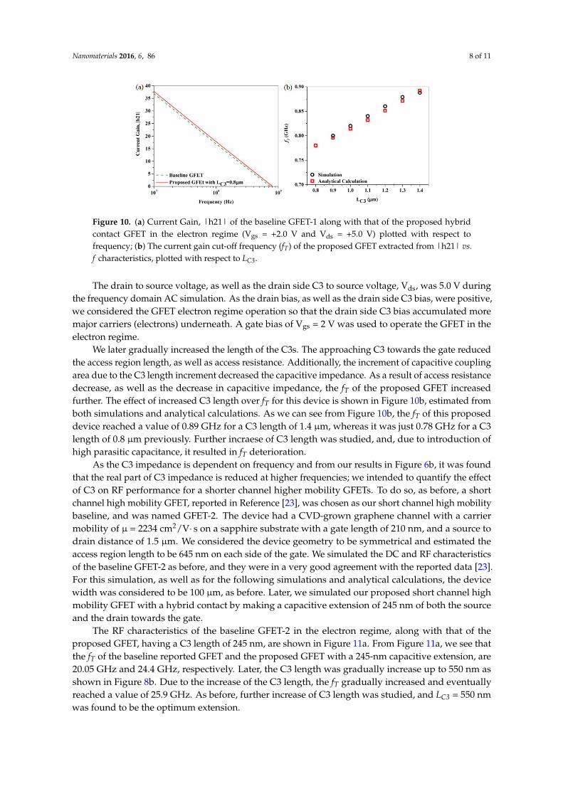
As the C3 impedance is dependent on frequency and from our results in Figure 6b, it was foundthat the real part of C3 impedance is reduced at higher frequencies; we intended to quantify the effectof C3 on RF performance for a shorter channel higher mobility GFETs. To do so, as before, a shortchannel high mobility GFET, reported in Reference [23], was chosen as our short channel high mobilitybaseline, and was named GFET-2. The device had a CVD-grown graphene channel with a carriermobility of µ = 2234 cm2/V¨ s on a sapphire substrate with a gate length of 210 nm, and a source todrain distance of 1.5 µm. We considered the device geometry to be symmetrical and estimated theaccess region length to be 645 nm on each side of the gate. We simulated the DC and RF characteristicsof the baseline GFET-2 as before, and they were in a very good agreement with the reported data [23].For this simulation, as well as for the following simulations and analytical calculations, the devicewidth was considered to be 100 µm, as before. Later, we simulated our proposed short channel highmobility GFET with a hybrid contact by making a capacitive extension of 245 nm of both the sourceand the drain towards the gate.
The RF characteristics of the baseline GFET-2 in the electron regime, along with that of theproposed GFET, having a C3 length of 245 nm, are shown in Figure 11a. From Figure 11a, we see thatthe fT of the baseline reported GFET and the proposed GFET with a 245-nm capacitive extension, are20.05 GHz and 24.4 GHz, respectively. Later, the C3 length was gradually increase up to 550 nm asshown in Figure 8b. Due to the increase of the C3 length, the fT gradually increased and eventuallyreached a value of 25.9 GHz. As before, further increase of C3 length was studied, and LC3 = 550 nmwas found to be the optimum extension.

Nanomaterials 2016, 6, 86 9 of 11
Nanomaterials 2016, 6, 86 8 of 10
Figure 10. (a) Current Gain, |h21| of the baseline GFET-1 along with that of the proposed hybrid
contact GFET in the electron regime (Vgs = +2.0 V and Vds = +5.0 V) plotted with respect to frequency.
(b) The current gain cut-off frequency (fT) of the proposed GFET extracted from |h21| vs. f
characteristics, plotted with respect to LC3.
As the C3 impedance is dependent on frequency and from our results in Figure 6b, it was found
that the real part of C3 impedance is reduced at higher frequencies; we intended to quantify the effect
of C3 on RF performance for a shorter channel higher mobility GFETs. To do so, as before, a short
channel high mobility GFET, reported in Reference [23], was chosen as our short channel high
mobility baseline, and was named GFET-2. The device had a CVD-grown graphene channel with a
carrier mobility of μ = 2234 cm2/V·s on a sapphire substrate with a gate length of 210 nm, and a source
to drain distance of 1.5 μm. We considered the device geometry to be symmetrical and estimated the
access region length to be 645 nm on each side of the gate. We simulated the DC and RF characteristics
of the baseline GFET-2 as before, and they were in a very good agreement with the reported data [23].
For this simulation, as well as for the following simulations and analytical calculations, the device
width was considered to be 100 μm, as before. Later, we simulated our proposed short channel high
mobility GFET with a hybrid contact by making a capacitive extension of 245 nm of both the source
and the drain towards the gate.
The RF characteristics of the baseline GFET-2 in the electron regime, along with that of the
proposed GFET, having a C3 length of 245 nm, are shown in Figure 11a. From Figure 11a, we see that
the fT of the baseline reported GFET and the proposed GFET with a 245-nm capacitive extension, are
20.05 GHz and 24.4 GHz, respectively. Later, the C3 length was gradually increase up to 550 nm as
shown in Figure 8b. Due to the increase of the C3 length, the fT gradually increased and eventually
reached a value of 25.9 GHz. As before, further increase of C3 length was studied, and LC3 = 550 nm
was found to be the optimum extension.
Figure 11. (a) Current Gain, |h21| of the baseline GFET-2 along with that of the proposed hybrid
contact GFET in the electron regime (Vgs = +0.6 V and Vds = +1.6 V) plotted with respect to frequency.
(b) The current gain cut-off frequency (fT) of the proposed GFET extracted from |h21| vs. f
characteristics, plotted with respect to LC3.
In addition to the C3 extension over the access region, we also simulated a GFET with the source
to drain distance the same as that of the baseline, but with a longer gate. The new length of the gate
Figure 11. (a) Current Gain, |h21| of the baseline GFET-2 along with that of the proposed hybridcontact GFET in the electron regime (Vgs = +0.6 V and Vds = +1.6 V) plotted with respect tofrequency; (b) The current gain cut-off frequency (fT) of the proposed GFET extracted from |h21| vs.f characteristics, plotted with respect to LC3.
In addition to the C3 extension over the access region, we also simulated a GFET with the sourceto drain distance the same as that of the baseline, but with a longer gate. The new length of the gatewas equal to old gate length plus 2LC3, Lg-new = Lg-old + 2LC3. From our simulations, we found that thisdevice does not show any improvement of fT, rather the fT deteriorates compared to the baseline GFET.The reason behind this deterioration is the increase in transit delay. Though the C3 is capacitivelycoupled to the channel, as the gate contact is, the switching of the device takes place in the gate, not inthe C3s. The increase of the gate length increased the transit delay, whereas the equal C3 extensionlength reduced the parasitic delay.
4. Conclusions
In this work, we have proposed and analyzed a novel geometry GFET with an ohmic source/drainand its capacitive extension towards a gate in order to overcome the set of limitations on itshigh-frequency performance that arises from contact resistance and access resistance. The extended partof the ohmic contacts over access region, not only reduces access region length and its correspondingaccess resistance, but also its capacitive coupling to the graphene channel provides a low resistancepath for the high frequency signal. From our analyses, we found that our proposed long channel lowmobility GFET with hybrid contacts has a current gain cutoff frequency that is 20% higher than theexperimental data reported in the literature for the same geometry GFET with conventional ohmiccontacts. On the other hand, the improvement for a short channel high mobility GFET with hybridcontacts was even more prominent, and had a current gain cutoff frequency 26.3% higher than that ofthe reported geometry conventional contact GFETs. The proposed devices would be easier to fabricatewith a higher tolerance, and suitable for high frequency analog applications.
Acknowledgments: This work is supported by National Science Foundation (NSF) CAREER program with theAward Number: 0955013 and Army Research Office (Grant No. W911NF-12-1-0071). Chowdhury Al-Amingratefully acknowledges the financial support provided by the Florida International University (FIU) GraduateSchool Dissertation Year Fellowship. Raju Sinha gratefully acknowledges the financial support provided by thePresidential Fellowship from Florida International University Graduate School.
Author Contributions: Nezih Pala conceived the idea. Nezih Pala and Chowdhury Al-Amin discussed the theoryand simulation method. Chowdhury Al-Amin designed, systematically investigated the device and carriedout the numerical simulations and analytical calculations. In addition to that, Chowdhury Al-Amin wrote themanuscript and prepared the figures. Nezih Pala edited the manuscript. Phani Kiran Vabbina, Mustafa Karabiyik,and Raju Sinha discussed the results and commented on the manuscript. Nezih Pala is the principal investigatorof the project.
Conflicts of Interest: The authors declare no conflict of interest.

Nanomaterials 2016, 6, 86 10 of 11
References
1. Tung, V.C.; Allen, M.J.; Yang, Y.; Kaner, R.B. High-throughput solution processing of large-scale graphene.Nat. Nanotechnol. 2009, 4, 25–29. [CrossRef] [PubMed]
2. Kim, S.; Nah, J.; Jo, I.; Shahrjerdi, D.; Colombo, L.; Yao, Z.; Tutuc, E.; Banerjee, S.K. Realization of a highmobility dual-gated graphene field effect transistor with Al2O3 dielectric. Appl. Phys. Lett. 2009, 94.[CrossRef]
3. Xia, F.; Mueller, T.; Lin, Y.; Valdes-Garcia, A.; Avouris, P. Ultrafast graphene photodetector. Nat. Nanotechnol.2009, 4, 839–843. [CrossRef] [PubMed]
4. Guo, Z.; Zhang, D.; Gong, X. Thermal conductivity of graphene nanoribbons. Appl. Phys. Lett. 2009, 95.[CrossRef]
5. Rafiee, J.; Mi, X.; Gullapalli, H.; Thomas, A.V.; Yavari, F.; Shi, Y.; Ajayan, P.M.; Koratkar, N.A. Wettingtransparency of graphene. Nat. Mater. 2012, 11, 217–222. [CrossRef] [PubMed]
6. Meric, I.; Han, M.Y.; Young, A.F.; Ozyilmaz, B.; Kim, P.; Shepard, K.L. Current saturation in zero-bandgap,top-gated graphene field-effect transistors. Nat. Nanotechnol. 2008, 3, 654–659. [CrossRef] [PubMed]
7. Singisetti, U. In0.53Ga0.47As MOSFETs with 5 nm Channel and Self-Aligned Source/Drain by MBERegrowth. Ph.D. Thesis, University of California, Santa Barbara, CA, USA, 2009.
8. Hong, S.K.; Jeon, S.C.; Hwang, W.S.; Cho, B.J. Resistance analysis and device design guideline for grapheneRF transistors. 2D Mater. 2015, 2. [CrossRef]
9. Lin, Y.; Chiu, H.; Jenkins, K.A.; Farmer, D.B.; Avouris, P.; Valdes-Garcia, A. Dual-gate graphene FETs with of50 GHz. IEEE Electron Device Lett. 2010, 31, 68–70.
10. Balci, O.; Kocabas, C. Rapid thermal annealing of graphene-metal contact. Appl. Phys. Lett. 2012, 101.[CrossRef]
11. Huang, B.; Zhang, M.; Wang, Y.; Woo, J. Contact resistance in top-gated graphene field-effect transistors.Appl. Phys. Lett. 2011, 99. [CrossRef]
12. Li, W.; Liang, Y.; Yu, D.; Peng, L.; Pernstich, K.P.; Shen, T.; Walker, A.H.; Cheng, G.; Hacker, C.A.; Richter, C.A.Ultraviolet/ozone treatment to reduce metal-graphene contact resistance. Appl. Phys. Lett. 2013, 102.[CrossRef]
13. Wessely, A.P.; Schwalke, U. 2nd generation bilayer graphene transistors for applications in nanoelectronics.In Proceedings of the 9th IEEE International Conference On Design & Technology of Integrated Systems inNanoscale Era (DTIS), Santorini, Greece, 6–8 May 2014.
14. Venugopal, A. Effect of Contacts, Graphene Type and Underlying Substrate on the Transport Properties ofGraphene. Ph.D. Thesis, The University of Texas at Dallas, Dallas, TX, USA, 1 May 2012.
15. Leong, W.S.; Gong, H.; Thong, J.T. Low-Contact-Resistance Graphene Devices with Nickel-Etched-GrapheneContacts. ACS Nano 2013, 8, 994–1001. [CrossRef] [PubMed]
16. Badmaev, A.; Che, Y.; Li, Z.; Wang, C.; Zhou, C. Self-aligned fabrication of graphene RF transistors withT-shaped gate. ACS Nano 2012, 6, 3371–3376. [CrossRef] [PubMed]
17. Peng, S.; Jin, Z.; Zhang, D.; Shi, J.; Wang, X.; Wang, S.; Liu, X.; Yu, G. Effect of source-gate spacing on directcurrent and radio frequency characteristic of graphene field effect transistor. Appl. Phys. Lett. 2015, 106.[CrossRef]
18. Al-Amin, C.; Vabbina, P.K.; Karabiyik, M.; Sinha, R.; Pala, N.; Choi, W. Improving high-frequencycharacteristics of graphene FETs by field-controlling electrodes. IEEE Electron Device Lett. 2013, 34, 1193–1195.[CrossRef]
19. Al-Amin, C.; Karabiyik, M.; Vabbina, P.; Sinha, R.; Pala, N. Field Controlled RF Graphene FETs with ImprovedHigh Frequency Performance. Solid State Electron. 2014, 95, 36–41. [CrossRef]
20. Al-Amin, C.; Sinha, R.; Pala, N.; Choi, W. Novel graphene FETs with field-controlling electrodes to improveRF performance. In Proceedings of the SPIE Defense Security, International Society for Optics and Photonics,Baltimore, MD, USA, 5 May 2014.
21. Simin, G.; Shur, M.S.; Gaska, R. 5-terminal THzGaN based transistor with field- and space-charge controlelectrodes. Int. J. High Speed Electron. Syst. 2009, 19, 7–14. [CrossRef]
22. Brockerhoff, W.; Heime, K.; Ploog, K.; Weimann, G.; Schlapp, W. Optimisation of modulation-dopedheterostructures for TEGFET operation at room temperature. Electron. Lett. 1984, 20, 615–617.
Nanomaterials 2016, 6, 86 11 of 11
23. Wang, H.; Hsu, A.; Lee, D.S.; Kim, K.K.; Kong, J.; Palacios, T. Delay analysis of graphene field-effecttransistors. IEEE Electron Device Lett. 2012, 33, 324–326. [CrossRef]
24. Tasker, P.J.; Hughes, B. Importance of source and drain resistance to the maximum f/sub T/ofmillimeter-wave MODFETs. IEEE Electron Device Lett. 1989, 10, 291–293. [CrossRef]
25. Di Bartolomeo, A.; Giubileo, F.; Romeo, F.; Sabatino, P.; Carapella, G.; Iemmo, L.; Schroeder, T.;Lupina, G. Graphene field effect transistors with niobium contacts and asymmetric transfer characteristics.Nanotechnology 2015, 26. [CrossRef] [PubMed]
26. Roy, S.C.D. Triple frequency impedance matching by frequency transformation. IETE J. Edu. 2014, 55, 47–51.27. Simin, G.; Yang, Z.; Koudymov, A.; Adivarahan, V.; Khan, M.A. III-nitride transistors with capacitively
coupled contacts. Appl. Phys. Lett. 2006, 89. [CrossRef]28. Pozar, D.M. Microwave Engineering, 4th ed.; John Wiley & Sons: Hoboken, NJ, USA, 2012; pp. 191–192.29. Nayfeh, O.M. Radio-frequency transistors using chemical-vapor-deposited monolayer graphene:
Performance, doping, and transport effects. IEEE Trans. Electron Devices 2011, 58, 2847–2853. [CrossRef]30. Silvaco. Available online: http://www.silvaco.com/products/tcad/device_simulation/atlas/atlas.html
(accessed on 15 April 2016).31. Atlas, D.S. Atlas User’s Manual; Silvaco International Software: Santa Clara, CA, USA, 2006.
© 2016 by the authors; licensee MDPI, Basel, Switzerland. This article is an open accessarticle distributed under the terms and conditions of the Creative Commons Attribution(CC-BY) license (http://creativecommons.org/licenses/by/4.0/).