Grains and grain boundaries in highly crystalline ... · Grains and grain boundaries in...
14
Supplementary Figure S1: Commonlyobserved shapes in MoS2 CVD. Optical micrographs of various CVD MoS2 crystal shapes found in different growths. a) Mozz triangles and 6point star grown on “clean” Si/SiO2 substrates. Note: the small gold marks are metal alignment marks that were deposited after growth. b) Mozz mirror twin crystal used for electrical devices in Figures 5ij. c) Szz triangles and 5 and 6point stars. d) Hexagons. e) Gearlike polycrystalline structures grown on “dirty” substrates. f) 3point stars grown on “dirty” substrates. ac) show the types of crystals achieved in large grain growth, while df) show the types of crystals grown as a result of dirty substrates or old precursors. Grains and grain boundaries in highly crystalline monolayer molybdenum disulphide SUPPLEMENTARY INFORMATION DOI: 10.1038/NMAT3633 NATURE MATERIALS | www.nature.com/naturematerials 1 © 2013 Macmillan Publishers Limited. All rights reserved.
Transcript of Grains and grain boundaries in highly crystalline ... · Grains and grain boundaries in...

Grains and grain boundaries in highly-crystalline monolayer molybdenum
disulfide
Supplementary Figure S1: Commonly-observed shapes in MoS2 CVD.
Optical micrographs of various CVD MoS2 crystal shapes found in different growths.
a) Mo-‐z-‐z triangles and 6-‐point star grown on “clean” Si/SiO2 substrates. Note: the
small gold marks are metal alignment marks that were deposited after growth. b)
Mo-‐z-‐z mirror twin crystal used for electrical devices in Figures 5i-‐j. c) S-‐z-‐z
triangles and 5-‐ and 6-‐point stars. d) Hexagons. e) Gear-‐like polycrystalline
structures grown on “dirty” substrates. f) 3-‐point stars grown on “dirty” substrates.
a-‐c) show the types of crystals achieved in large grain growth, while d-‐f) show the
types of crystals grown as a result of dirty substrates or old precursors.
Grains and grain boundaries in highly crystalline monolayer molybdenum disulphide
SUPPLEMENTARY INFORMATIONDOI: 10.1038/NMAT3633
NATURE MATERIALS | www.nature.com/naturematerials 1
© 2013 Macmillan Publishers Limited. All rights reserved.

Supplementary Figure S2: Continuous sheet
Figure S2a-‐b show optical images from two different, yet typical, samples similar to
Figure 1a. The key difference between the samples is the grain size. On the top left in
each image is bare oxide with sparse crystals. In both samples, CVD MoS2 crystals
can grow together to form continuous monolayer sheets (bottom right). The
2 NATURE MATERIALS | www.nature.com/naturematerials
SUPPLEMENTARY INFORMATION DOI: 10.1038/NMAT3633
© 2013 Macmillan Publishers Limited. All rights reserved.

gradients in nucleation density and grain size reflect the substrate proximity to the
solid MoO3 source. The small gold and orange dots, indicated by a red circle, are
alignment marks placed after growth. Figure S2c shows two representative
histograms of island size (as the square root of the area) extracted from portions of
Figure 1a and Figure S2a. In the larger grain growths, such as in Figure S2b, the
triangles grow together more to form aggregates and continuous sheets, making
accurate measurement of grain size impossible without crystalographically
sensitive techniques; For this reason only isolated islands in smaller-‐grain growths
are included in Figure S2c, and regions near continuous sheets are excluded from
the measurement. The spread in the histogram demonstrate the wide range of
grain sizes and spatial inhomogeneity in all of our samples.
NATURE MATERIALS | www.nature.com/naturematerials 3
SUPPLEMENTARY INFORMATIONDOI: 10.1038/NMAT3633
© 2013 Macmillan Publishers Limited. All rights reserved.

Supplementary Figure S3: Raman spectra and mapping
a) Raman spectra showing the E2g1 and A1g vibrational modes1 for monolayer (red
curve) and bilayer (blue curve) MoS2 corresponding with the photoluminescence
spectra from Figure 1c. b-‐c) Maps of the peak position for the two Raman modes for
monolayer tilt boundary from Figure 5 where b) represents the E2g1 mode. and c)
represents the A1g mode. Both modes show an upshift of 1 cm-‐1 at the grain
boundary. While this shift may indicate a change in strain or doping at the
boundary, it is difficult to interpret compared to the more marked changes to the
photoluminescence seen in Figure 5 of the main text. Scale bar 5 µm.
4 NATURE MATERIALS | www.nature.com/naturematerials
SUPPLEMENTARY INFORMATION DOI: 10.1038/NMAT3633
© 2013 Macmillan Publishers Limited. All rights reserved.
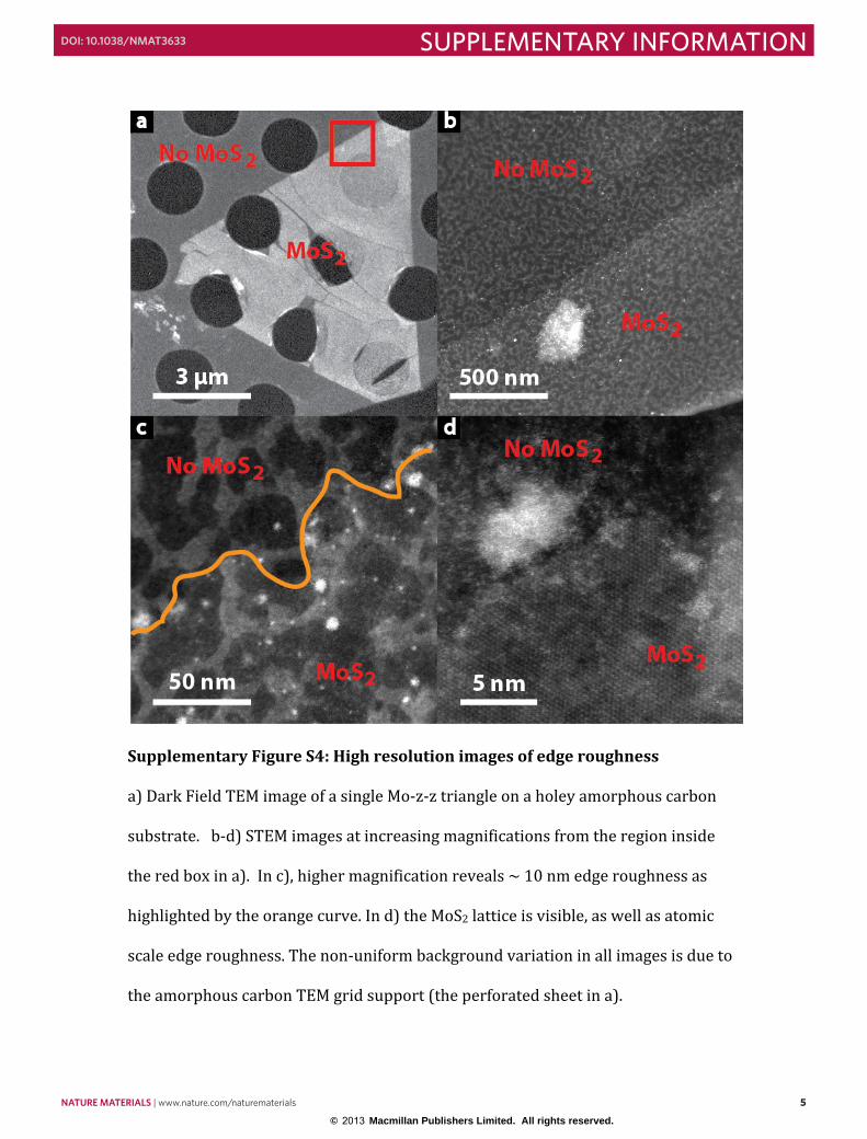
Supplementary Figure S4: High resolution images of edge roughness
a) Dark Field TEM image of a single Mo-‐z-‐z triangle on a holey amorphous carbon
substrate. b-‐d) STEM images at increasing magnifications from the region inside
the red box in a). In c), higher magnification reveals ~ 10 nm edge roughness as
highlighted by the orange curve. In d) the MoS2 lattice is visible, as well as atomic
scale edge roughness. The non-‐uniform background variation in all images is due to
the amorphous carbon TEM grid support (the perforated sheet in a).
NATURE MATERIALS | www.nature.com/naturematerials 5
SUPPLEMENTARY INFORMATIONDOI: 10.1038/NMAT3633
© 2013 Macmillan Publishers Limited. All rights reserved.

Supplementary Figure S5: DF-TEM imaging of cyclic twin
a) Bright-‐field image of a 6-‐pointed star. b) Full diffraction pattern shows star has
no rotational boundaries. c-‐e) Dark-‐field TEM images corresponding with the c) red,
d) blue, e) orange spots in the diffraction image. The red and blue [-‐1100] spots
show opposite intensity because they swap whether the ka or kb spot is captured for
each region. The orange spot shows an even intensity over the entire star; this
occurs because unlike the [-‐1100] spots, the intensity of the [-‐2110] spots are 6-‐fold
symmetric (See Figure 1c). f) Bright-‐field TEM image with overlaid edge
orientations extracted from DF-‐TEM. The outer edges are oriented along the Mo-‐z-‐z
direction, which demonstrates that the grain boundaries are oriented along the S-‐z-‐z
directions.
6 NATURE MATERIALS | www.nature.com/naturematerials
SUPPLEMENTARY INFORMATION DOI: 10.1038/NMAT3633
© 2013 Macmillan Publishers Limited. All rights reserved.

Supplementary Figure S6: Simulations of alternate mirror-twin boundaries
a) Geometry optimized structure for the experimentally observed grain boundary,
as determined by DFT (a). b) The local DOS (LDOS) integrated in the plane of the Mo
over a 1.7 eV window inside the band gap of pristine MoS2 confirms the spatial
localization of mid-‐gap states. c) The energy-‐resolved density of states for pristine
MoS2 (black curve), the DOS of the structure shown in (a) (red curve), and the DOS
projected just onto the atoms in the grain boundary (blue curve). In (c), we have
subtracted off the contribution to the DOS arising from the unphysical edge atoms.
NATURE MATERIALS | www.nature.com/naturematerials 7
SUPPLEMENTARY INFORMATIONDOI: 10.1038/NMAT3633
© 2013 Macmillan Publishers Limited. All rights reserved.

Analogous calculations are shown for an armchair grain boundary d-‐f) and for a zig-‐
zag grain boundary g-‐i); both which are entirely periodic in two dimensions. In
panels (b), (e), and (h), the colorscale indicates the magnitude of the integrated
LDOS, from 0 (dark) to 0.025 bohr-‐3 (light).
Supplementary Figure S7: Time resolved photoluminescence
Time-‐resolved photoluminescence measurements obtained by time-‐correlated
single photon counting with femtosecond excitation by 400-‐nm laser pulses.
Results for exfoliated and CVD MoS2 samples on oxide layers, after accounting for
the instrument response function, yield nearly identical time constants of
τexfoliated=44 ps, and τCVD=42 ps. The measured emission decay found to varied
considerably from sample to sample for both the exfoliated and CVD grown
8 NATURE MATERIALS | www.nature.com/naturematerials
SUPPLEMENTARY INFORMATION DOI: 10.1038/NMAT3633
© 2013 Macmillan Publishers Limited. All rights reserved.

materials, so the similarity of the curves in this figure should not be regarded as
having fundamental significance.
Supplementary Figure S8: Electrical measurements on a tilt boundary
a) Linear and b) logarithmic electrical transport transfer curves of 3 FETs fabricated
from the tilt boundary MoS2 island shown in the inset of (a), which has a tilt angle of
42° (Scale bar 10 μm). The FETs containing the perpendicular (black) and parallel
(orange) boundary orientation to the flow of electrons are both 30% lower in
conductance than the pristine region (cyan) in the “on” state (gate voltage = +70 V).
NATURE MATERIALS | www.nature.com/naturematerials 9
SUPPLEMENTARY INFORMATIONDOI: 10.1038/NMAT3633
© 2013 Macmillan Publishers Limited. All rights reserved.

Supplementary Methods:
Electron Diffraction Simulation:
We calculated the diffraction pattern for a monolayer of MoS2 using Bloch wave
simulations to account for the complex scattering that allows the breaking of
Friedel’s rule and produces this asymmetry (Figure 2). The asymmetry of the Mo
and S sublattices separates the [-‐1100] diffraction spots into two families : ka={(-‐
1100), (10-‐10), (0-‐110)} and kb= -ka. Our bloch-‐wave simulations show that the
~10% higher intensity ka spots point toward the Mo sublattice, as indicated by the
arrows in Figures 2(a-‐b). We double-‐checked this result with high-‐resolution
imaging to confirm that the asymmetric diffraction pattern in Fig 2(b) corresponds
to the indicated orientation of the MoS2 lattice.
Identifying triangle edge terminations:
Via TEM analyses, we consistently observe that Mo-‐z-‐z triangles (Figure 2(b)) have
sharper and straighter edges than S-‐z-‐z triangles (Figure 2(d)). This morphological
difference allows us to rapidly identify the crystal edges and orientation of triangles
on the growth substrate simply by optical microscopy. In doing so, we also observe
that all crystals from the same growth run have the same morphology, i.e., triangles
from a given run will either be dominated by Mo-‐z-‐z or by S-‐z-‐z edges, a preference
we attribute to kinetic effects. Both triangle morphologies exhibit the same range of
average sizes from 30-‐70 µm. These classifications are important for understanding
10 NATURE MATERIALS | www.nature.com/naturematerials
SUPPLEMENTARY INFORMATION DOI: 10.1038/NMAT3633
© 2013 Macmillan Publishers Limited. All rights reserved.

growth dynamics and suggest the possibility of refined control of edge morphology
by tuning the CVD process.
DFT calculations:
Density functional theory (DFT) calculations were performed with the PW91
generalized gradient approximation for the exchange-‐correlation functional and
ultrasoft pseudopotentials, as implemented in the Quantum Espresso electronic
structure package5. Supercells were generated with about 10 Å separation to
ensure negligible interactions between replicas. Structural relaxations were carried
out at the gamma point until all components of all forces were less than 0.001 a.u.
Pristine MoS2 (3.12 and 2.32 Å for Mo-‐Mo and Mo-‐S bond lengths, respectively)
energy calculations were done with a 16x16 Monkhorst-‐type k-‐point grid,
confirming the material's direct band gap with a predicted energy of 1.9 eV.
Preliminary calculations employing a finer k-‐point grid for the structural relaxation
show minor quantitative but not qualitative changes to the grain boundary
geometry and electron structure6.
Because the direction of the experimentally observed 8-‐4-‐4 grain boundary is
incommensurate with the periodicity of the underlying crystal, a system periodic in
two dimensions cannot be constructed. Thus we employed the system shown in
Figure S6(a) which is periodic along the direction of the grain boundary, but finite in
the orthogonal direction such that the edge, terminated by S dimers, is about 10 Å
NATURE MATERIALS | www.nature.com/naturematerials 11
SUPPLEMENTARY INFORMATIONDOI: 10.1038/NMAT3633
© 2013 Macmillan Publishers Limited. All rights reserved.

away from the grain boundary. Energy calculations for this 87-‐atom supercell were
performed with 5 k-‐points in the periodic direction. Local density of states (LDOS)
analysis, shown in Figure S6(b) confirms that the electronic effects of the artificial
edges are physically confined along the perimeter and so should not affect the
properties along the grain boundary. These conclusions are also corroborated by a
negligible change in bond length, compared to the bulk, for atoms away from the
grain boundary. Analogous calculations on 2D periodic systems with pure armchair
and zig-‐zag grain boundaries, shown in Figure S6 (d-‐i) similarly yield mid-‐gap states
localized along the boundary, further indicating that the effect is generic and not an
artifact of the finite strip size.
Estimating non-radiative recombination:
Photoluminescence quenching commonly arises from defects in semiconductors,
such as the predicted midgap states at the boundaries, which can act as centers for
non-‐radiative recombination7. While the amount of material structurally modified
by the boundary is small compared with the 500-‐nm laser spot size, the effect can be
enhanced by the diffusion of photogenerated excitons to the boundary, which
effectively increases the boundary width. Such a process would provide a natural
explanation for the strongly reduced PL observed from some boundaries in our
samples, since non-‐radiative recombination may be more efficient in the presence of
the localized structures and states of the boundary. Here we estimate the potential
impact of this effect using measured values for the carrier mobility and exciton
lifetime.
12 NATURE MATERIALS | www.nature.com/naturematerials
SUPPLEMENTARY INFORMATION DOI: 10.1038/NMAT3633
© 2013 Macmillan Publishers Limited. All rights reserved.

The electrical measurements in this paper yielded an electron mobility of µe = 3
cm2V-‐1s-‐1 for typical CVD-‐grown samples. From the Einstein relation for a
temperature of T = 300 K, we then obtain an electron diffusivity of = 8
x 10-‐2 cm2s-‐1. Since the electron and hole masses are similar, we assume that the
exciton diffusivity is half of the electron diffusivity, i.e., Dexc = 4 x 10-‐2 cm2s-‐1. The
scattering mechanisms for electrons and excitons need not be the same, so this
should only be considered as an estimate.
The characteristic length for diffusion of excitons towards the boundary from the 2-‐
D bulk material over a time τ is given by . For a time interval of τ = 40
ps reported above for the exciton lifetime, we then infer a diffusion length of L = 24
nm. This length, while not negligible, is small compared to the 500 nm spot size of
the excitation laser. The quenching of the PL by 50% observed at some grain
boundaries must consequently rely primarily, as discussed in the main text, on
mechanisms other than exciton diffusion.
Supplementary References:
1 Lee, C. et al. Anomalous Lattice Vibrations of Single-‐ and Few-‐Layer MoS2. ACS Nano 4, 2695-‐2700.
2 Huang, P. Y. et al. Grains and grain boundaries in single-‐layer graphene atomic patchwork quilts. Nature 469, 389-‐392 (2011).
3 Kim, K. et al. Grain Boundary Mapping in Polycrystalline Graphene. ACS Nano 5, 2142-‐2146 (2011).
4 Lahiri, J., Lin, Y., Bozkurt, P., Oleynik, I. I. & Batzill, M. An extended defect in graphene as a metallic wire. Nature Nanotechnology 5, 326-‐329 (2010).
NATURE MATERIALS | www.nature.com/naturematerials 13
SUPPLEMENTARY INFORMATIONDOI: 10.1038/NMAT3633
© 2013 Macmillan Publishers Limited. All rights reserved.

5 Paolo, G. et al. QUANTUM ESPRESSO: a modular and open-‐source software project for quantum simulations of materials. Journal of Physics: Condensed Matter 21, 395502 (2009).
6 J. Kunstmann, T. B., D. Reichman. Unpublished results. 7 Neamen, D. A. Semiconductor physics and Devices. (McGraw-‐Hill, 2002).
14 NATURE MATERIALS | www.nature.com/naturematerials
SUPPLEMENTARY INFORMATION DOI: 10.1038/NMAT3633
© 2013 Macmillan Publishers Limited. All rights reserved.


![Crystal Plasticity Modeling of Anisotropic Hardening and ... · Similar to the Basinski mechanism [25], the capacity of dislocations to transmute from parent grains across twin boundaries](https://static.fdocuments.in/doc/165x107/5f59a8d12c44fc46f35ec8f2/crystal-plasticity-modeling-of-anisotropic-hardening-and-similar-to-the-basinski.jpg)