
GPU vs Xeon Phi: Performance of Bandwidth Bound Applications...
46
GTC 2015 | Mathias Wagner | Indiana University | GPU vs Xeon Phi: Performance of Bandwidth Bound Applications with a Lattice QCD Case Study Mathias Wagner
Transcript of GPU vs Xeon Phi: Performance of Bandwidth Bound Applications...

GTC 2015 | Mathias Wagner | Indiana University |
GPU vs Xeon Phi: Performance of Bandwidth Bound Applications with a Lattice QCD Case Study
Mathias Wagner

GTC 2015 | Mathias Wagner | Indiana University |
Lattice Quantum ChromoDynamics
and Deep Learning …
… sorry, not (yet?) here.

GTC 2015 | Mathias Wagner | Indiana University |
Lattice QCD: Some Basics
•QCD partition function
•4 dimensional grid (=Lattice)
•quarks live on lattice sites
•gluons live on the links
•typical sizes: 243 x 6 to 2564
•parallelization over lattice sites (105 to 109)
Formulating Lattice QCD
• Quark fields live on the lattice sites
• “spinors”
• 12 complex numbers
• Gluon fields live on the links
• SU(3) “Color matrices”
• 18 complex numbers
Friday, 11 March 2011
ZQCD (T, µ) =
ZDAD�D�e�SE(T,µ)
includes integral over space and time

GTC 2015 | Mathias Wagner | Indiana University |
Mapping the Wilson-Clover operator to CUDA
• Each thread must
• Load the neighboring spinor (24 numbers x8)
• Load the color matrix connecting the sites (18 numbers x8)
• Load the clover matrix (72 numbers)
• Save the result (24 numbers)
• Arithmetic intensity
• 3696 floating point operations per site
• 2976 bytes per site (single precision)
• 1.24 naive arithmetic intensity
review basic details of the LQCD application and of NVIDIAGPU hardware. We then briefly consider some related workin Section IV before turning to a general description of theQUDA library in Section V. Our parallelization of the quarkinteraction matrix is described in VI, and we present anddiscuss our performance data for the parallelized solver inSection VII. We finish with conclusions and a discussion offuture work in Section VIII.
II. LATTICE QCDThe necessity for a lattice discretized formulation of QCD
arises due to the failure of perturbative approaches commonlyused for calculations in other quantum field theories, such aselectrodynamics. Quarks, the fundamental particles that are atthe heart of QCD, are described by the Dirac operator actingin the presence of a local SU(3) symmetry. On the lattice,the Dirac operator becomes a large sparse matrix, M , and thecalculation of quark physics is essentially reduced to manysolutions to systems of linear equations given by
Mx = b. (1)
The form of M on which we focus in this work is theSheikholeslami-Wohlert [6] (colloquially known as Wilson-clover) form, which is a central difference discretization of theDirac operator. When acting in a vector space that is the tensorproduct of a 4-dimensional discretized Euclidean spacetime,spin space, and color space it is given by
Mx,x0 = �12
4⇤
µ=1
�P�µ ⇤ Uµ
x �x+µ,x0 + P+µ ⇤ Uµ†x�µ �x�µ,x0
⇥
+ (4 + m + Ax)�x,x0
⌅ �12Dx,x0 + (4 + m + Ax)�x,x0 . (2)
Here �x,y is the Kronecker delta; P±µ are 4 ⇥ 4 matrixprojectors in spin space; U is the QCD gauge field whichis a field of special unitary 3⇥ 3 (i.e., SU(3)) matrices actingin color space that live between the spacetime sites (and henceare referred to as link matrices); Ax is the 12⇥12 clover matrixfield acting in both spin and color space,1 corresponding toa first order discretization correction; and m is the quarkmass parameter. The indices x and x⇥ are spacetime indices(the spin and color indices have been suppressed for brevity).This matrix acts on a vector consisting of a complex-valued12-component color-spinor (or just spinor) for each point inspacetime. We refer to the complete lattice vector as a spinorfield.
Since M is a large sparse matrix, an iterative Krylovsolver is typically used to obtain solutions to (1), requiringmany repeated evaluations of the sparse matrix-vector product.The matrix is non-Hermitian, so either Conjugate Gradients[7] on the normal equations (CGNE or CGNR) is used, ormore commonly, the system is solved directly using a non-symmetric method, e.g., BiCGstab [8]. Even-odd (also known
1Each clover matrix has a Hermitian block diagonal, anti-Hermitian blockoff-diagonal structure, and can be fully described by 72 real numbers.
Fig. 1. The nearest neighbor stencil part of the lattice Dirac operator D,as defined in (2), in the µ� � plane. The color-spinor fields are located onthe sites. The SU(3) color matrices Uµ
x are associated with the links. Thenearest neighbor nature of the stencil suggests a natural even-odd (red-black)coloring for the sites.
as red-black) preconditioning is used to accelerate the solutionfinding process, where the nearest neighbor property of theDx,x0 matrix (see Fig. 1) is exploited to solve the Schur com-plement system [9]. This has no effect on the overall efficiencysince the fields are reordered such that all components ofa given parity are contiguous. The quark mass controls thecondition number of the matrix, and hence the convergence ofsuch iterative solvers. Unfortunately, physical quark massescorrespond to nearly indefinite matrices. Given that currentleading lattice volumes are 323 ⇥ 256, for > 108 degrees offreedom in total, this represents an extremely computationallydemanding task.
III. GRAPHICS PROCESSING UNITS
In the context of general-purpose computing, a GPU iseffectively an independent parallel processor with its ownlocally-attached memory, herein referred to as device memory.The GPU relies on the host, however, to schedule blocks ofcode (or kernels) for execution, as well as for I/O. Data isexchanged between the GPU and the host via explicit memorycopies, which take place over the PCI-Express bus. The low-level details of the data transfers, as well as management ofthe execution environment, are handled by the GPU devicedriver and the runtime system.
It follows that a GPU cluster embodies an inherently het-erogeneous architecture. Each node consists of one or moreprocessors (the CPU) that is optimized for serial or moderatelyparallel code and attached to a relatively large amount ofmemory capable of tens of GB/s of sustained bandwidth. Atthe same time, each node incorporates one or more processors(the GPU) optimized for highly parallel code attached to arelatively small amount of very fast memory, capable of 150GB/s or more of sustained bandwidth. The challenge we face isthat these two powerful subsystems are connected by a narrowcommunications channel, the PCI-E bus, which sustains atmost 6 GB/s and often less. As a consequence, it is criticalto avoid unnecessary transfers between the GPU and the host.
Dx,x
0 = A =
Friday, 11 March 2011
Staggered Fermion Matrix (Dslash)
•Krylov space inversion of fermion matrix dominates runtime
•within inversion application of sparse Matrix (Dslash) dominates (>80%)
•Highly Improved Staggered Quarks (HISQ) use next and 3rd neighbor stencil
•each site (x) loads 1024 bytes for links and 384 bytes for vectors, stores 24 bytes: total 1432 bytes / site
•performs 1146 flop: arithmetic intensity: 0.8 flop/bytesensitive to memory bandwidth
wx
= Dx,x
0vx
0 =3
X
µ=0
hn
Ux,µ
vx+µ
� U †x�µ,µ
vx�µ
o
+n
Nx,µ
vx+3µ �N†
x�3µ,µvx�3µ
oi
complex 3x3 matrix72 byte for fp32
complex 3x3 matrix + U(3) symmetry56 byte for fp32
complex 3-dim vector24 byte for fp32complex 3-dim vector24 byte for fp32

GTC 2015 | Mathias Wagner | Indiana University |
Accelerators
Sorry, not the ones with liquid helium cooling and TDP > 300W.

GTC 2015 | Mathias Wagner | Indiana University |
Intel Xeon Phi and Nvidia Tesla
5110 7120 K20 K20X K40Cores / SMX 60 61 13 14 15
Vector instructions 512 bit (16 fp32)CUDA cores / SMX 192
Clock Speed [MHz] 1053 1238 - 1333 705 732 745-875 peak fp32 [TFlop/s] 2.02 2.42 3.52 3.91 4.29 peak fp64 [TFlop/s] 1.01 1.21 1.27 1.31 1.43
Memory [GB] 8 8 5 6 12 Memory Bandwidth [GB/s] 320 352 208 250 288 L1 Cache [kB] / (Core/SMX)
[kB]32 16-48 + 48 (Texture)
L2 Cache [MB] 30 (60 x 0.5) 30.5 (61 x 0.5) 1.5 TDP [W] 225 300 225 235 235
How can we achieve this performance?
How can we saturate the available bandwidth?
How much energy does that require?

GTC 2015 | Mathias Wagner | Indiana University |
Setting the bar
What performance can we expect on the different accelerators?Is our code optimized?
GTC 2015 | Mathias Wagner | Indiana University |
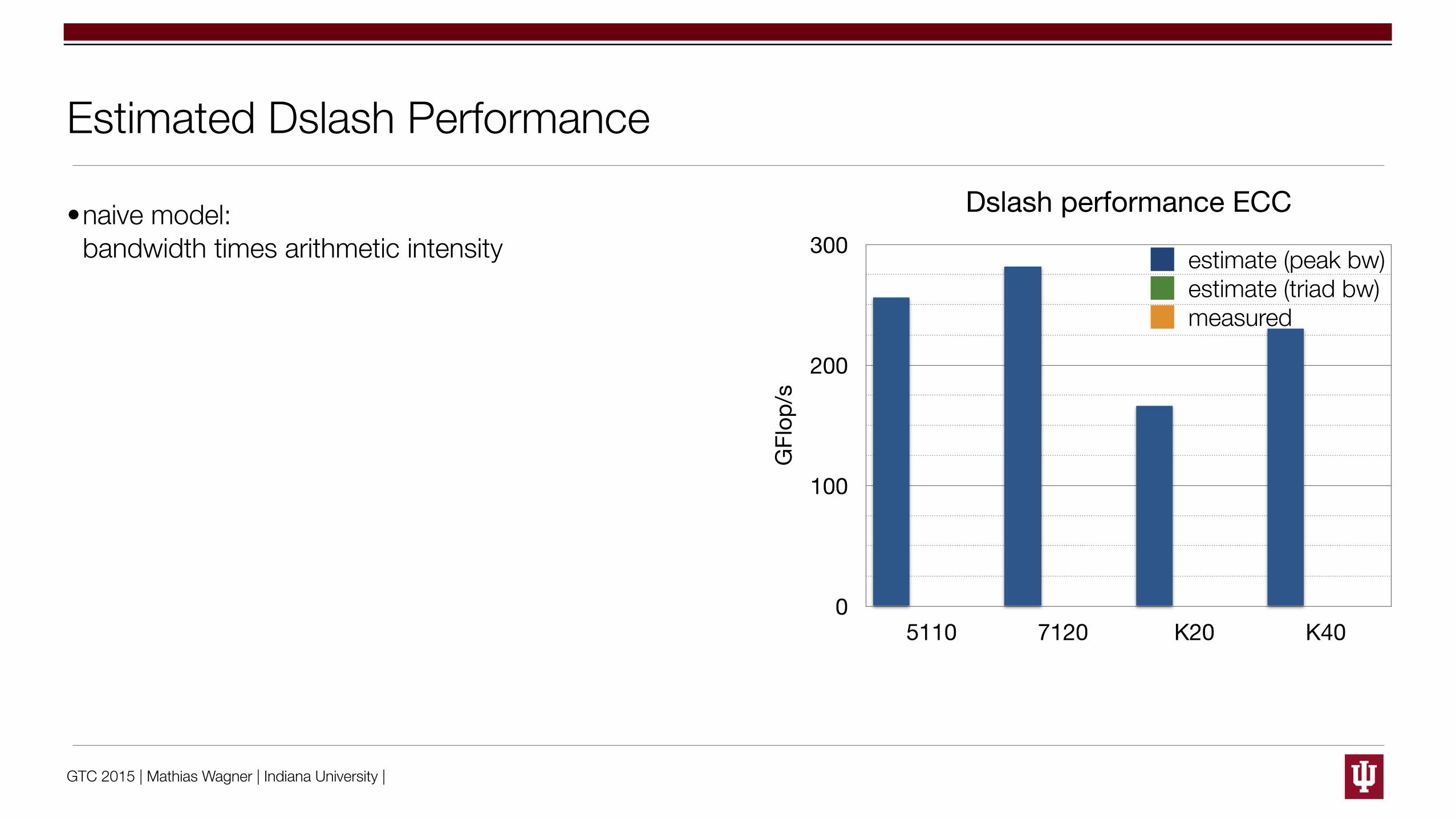
Estimated Dslash Performance
•naive model:bandwidth times arithmetic intensity
Dslash performance ECC
GFl
op/s
0
100
200
300
5110 7120 K20 K40
estimate (peak bw)estimate (triad bw)measured
GTC 2015 | Mathias Wagner | Indiana University |
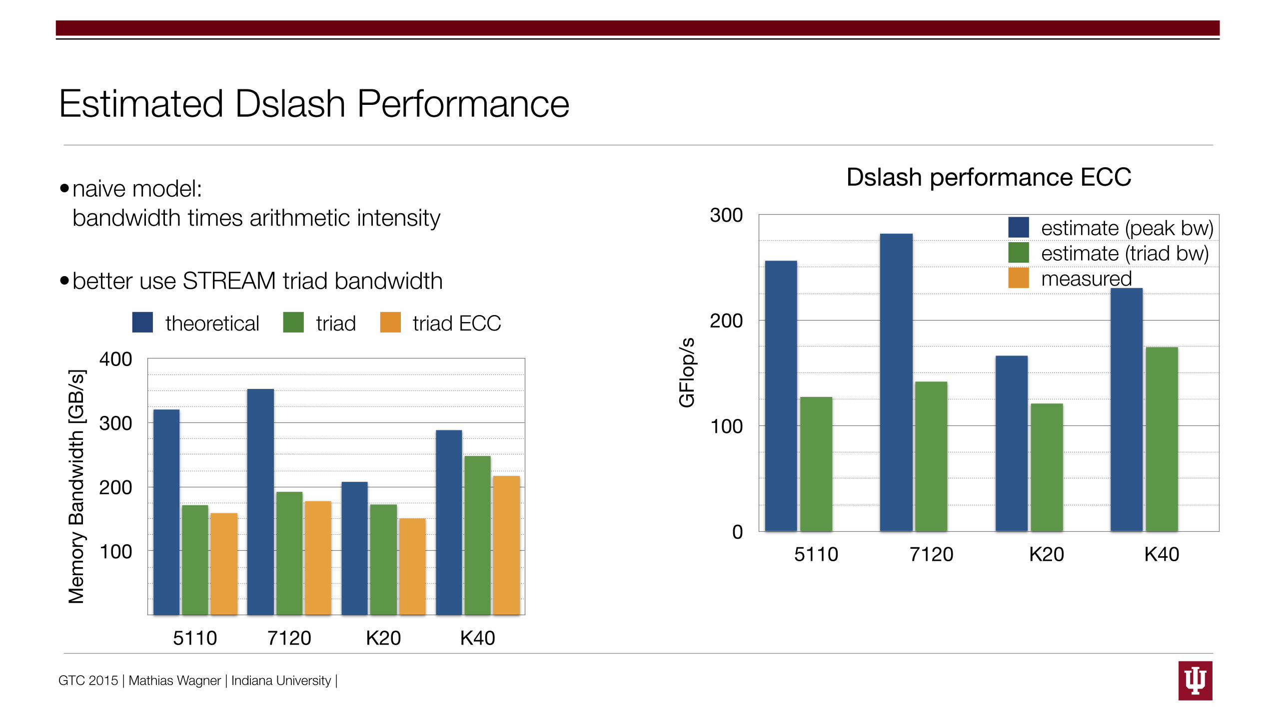
Estimated Dslash Performance
•naive model:bandwidth times arithmetic intensity
•better use STREAM triad bandwidth
Dslash performance ECC
GFl
op/s
0
100
200
300
5110 7120 K20 K40
estimate (peak bw)estimate (triad bw)measured
Mem
ory
Band
wid
th [G
B/s]
100
200
300
400
5110 7120 K20 K40
theoretical triad triad ECC

GTC 2015 | Mathias Wagner | Indiana University |
Estimated Dslash Performance
•naive model:bandwidth times arithmetic intensity
•better use STREAM triad bandwidth
•faster than estimate from triad bandwidth
Dslash performance ECC
GFl
op/s
0
100
200
300
5110 7120 K20 K40
estimate (peak bw)estimate (triad bw)measured
account for existence of cache in estimate of performance
GTC 2015 | Mathias Wagner | Indiana University |
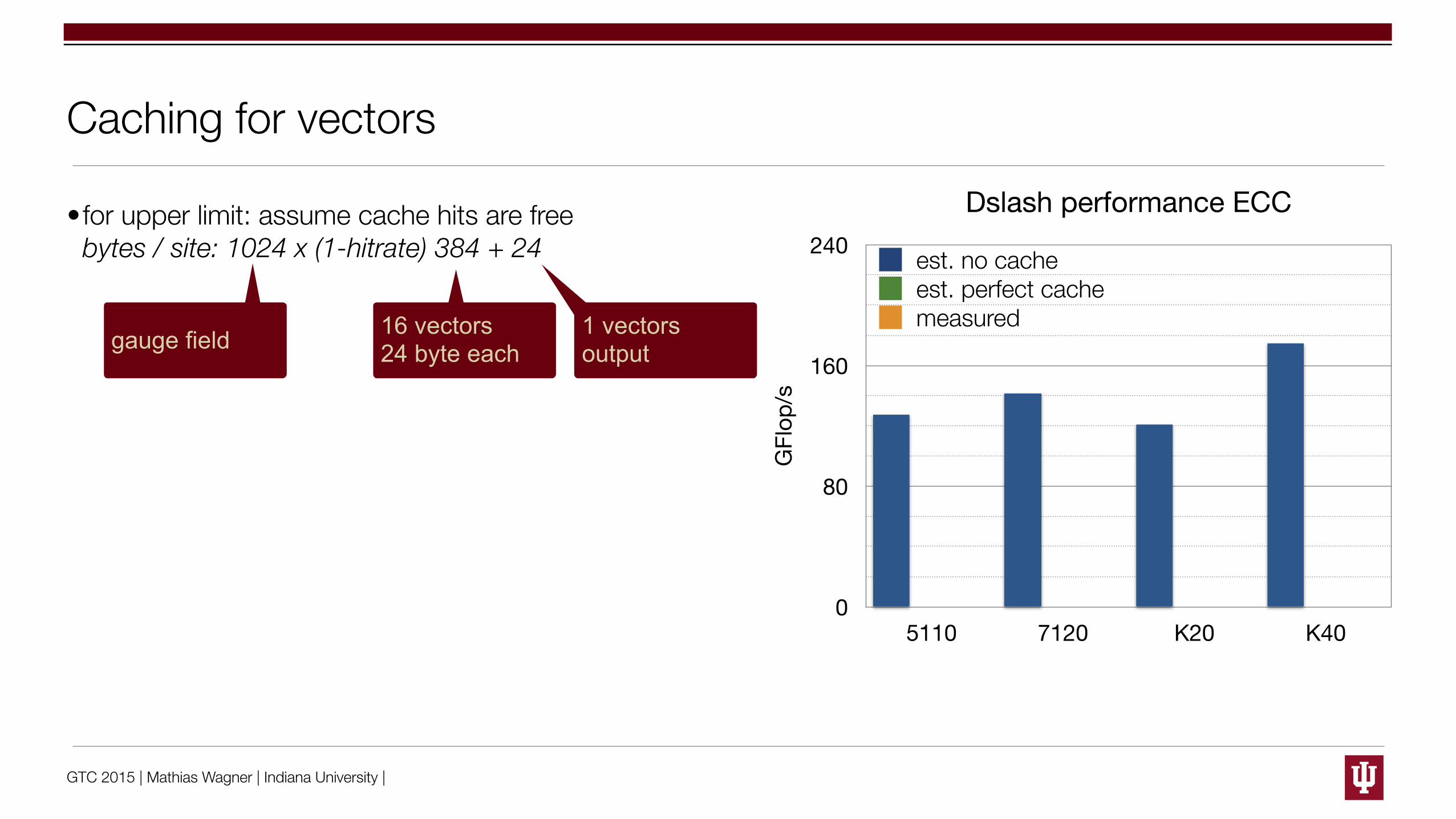
Caching for vectors
•for upper limit: assume cache hits are free bytes / site: 1024 x (1-hitrate) 384 + 24
Dslash performance ECC
GFl
op/s
0
80
160
240
5110 7120 K20 K40
est. no cacheest. perfect cachemeasured
gauge field 16 vectors24 byte each
1 vectorsoutput

GTC 2015 | Mathias Wagner | Indiana University |
Caching for vectors
•for upper limit: assume cache hits are free bytes / site: 1024 x (1-hitrate) 384 + 24
•Perfect caching scenario: hit for 15 out of 16 input vectors → arithmetic intensity 1.07 (w/o cache 0.80)
•typical size of a vector: 323x8 → 3MB, 643x16 → 24MB
•KNC: ~30 MB L2 (512 kB / core) + 32kB L1 / core [60 cores]
•Kepler: 1.5MB L2+ (16-48) kB L1 / SMX [15 SMX]
Dslash performance ECC
GFl
op/s
0
80
160
240
5110 7120 K20 K40
est. no cacheest. perfect cachemeasured
gauge field 16 vectors24 byte each
1 vectorsoutput
GTC 2015 | Mathias Wagner | Indiana University |
GPU Memory System
© 2013, NVIDIA 36
DRAM
L2
SM
L1 Read only
Const
SM • Once in an SM, data goes into one of 3 caches/buffers
• Programmer’s choice – L1 is the “default”
– Read-only, Const require explicit code
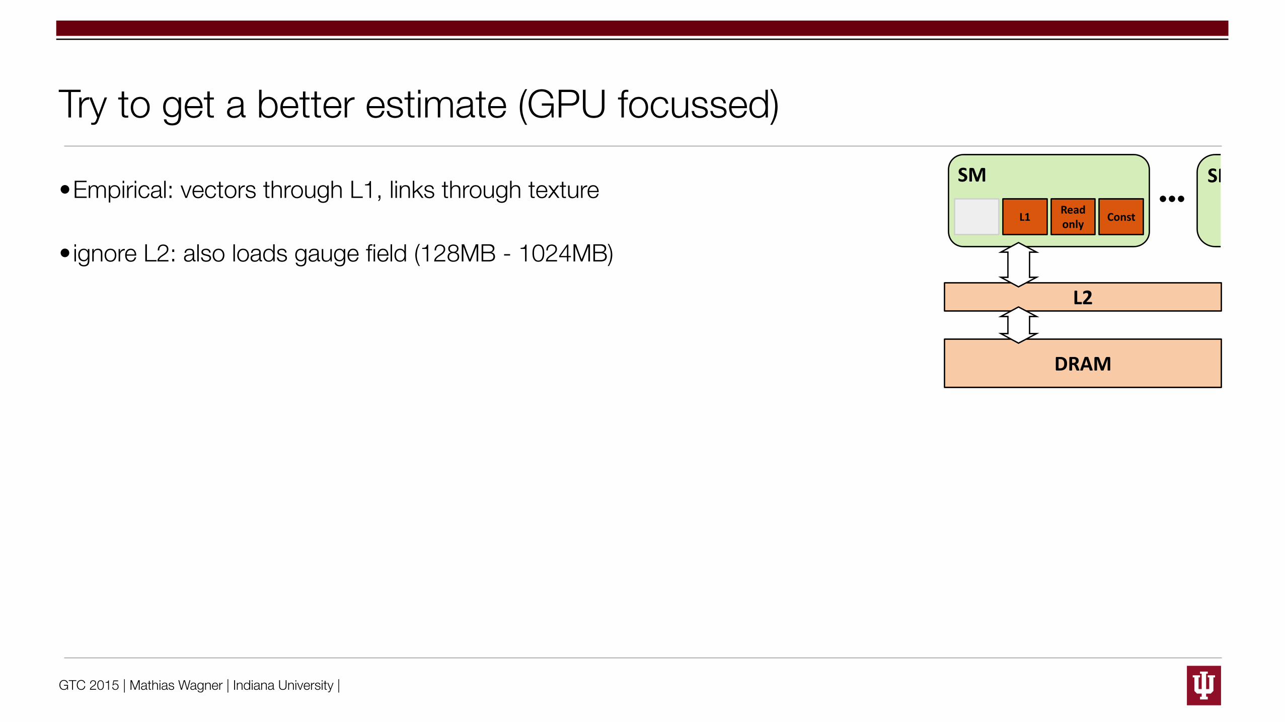
Try to get a better estimate (GPU focussed)
•Empirical: vectors through L1, links through texture
•ignore L2: also loads gauge field (128MB - 1024MB)

GTC 2015 | Mathias Wagner | Indiana University |
Try to get a better estimate (GPU focussed)
•Empirical: vectors through L1, links through texture
•ignore L2: also loads gauge field (128MB - 1024MB)
•48 kB L1 can hold 2048 24-byte vector elements
•for 643x16: 1 xy-plane (even-odd precondition)hit 7 out of 16 (43% hit rate)
•for 323x8: xy plane has 512 elements → 4 xy-planesin z direction we can hit 2 of 4 elements: 9/16 (56% hit rate)

GTC 2015 | Mathias Wagner | Indiana University |
z-di
rect
ion
L1
Try to get a better estimate (GPU focussed)
•Empirical: vectors through L1, links through texture
•ignore L2: also loads gauge field (128MB - 1024MB)
•48 kB L1 can hold 2048 24-byte vector elements
•for 643x16: 1 xy-plane (even-odd precondition)hit 7 out of 16 (43% hit rate)
•for 323x8: xy plane has 512 elements → 4 xy-planesin z direction we can hit 2 of 4 elements: 9/16 (56% hit rate)
hit rate 0/16 15/16 3/16 5/16 7/16 9/16
arithmetic intensity 0.8 1.07 0.84 0.87 0.91 0.94

GTC 2015 | Mathias Wagner | Indiana University |
Try to get a better estimate (GPU focussed)
•Empirical: vectors through L1, links through texture
•ignore L2: also loads gauge field (128MB - 1024MB)
•48 kB L1 can hold 2048 24-byte vector elements
•for 643x16: 1 xy-plane (even-odd precondition)hit 7 out of 16 (43% hit rate)
•for 323x8: xy plane has 512 elements → 4 xy-planesin z direction we can hit 2 of 4 elements: 9/16 (56% hit rate)
Dslash performance K40 ECC, 32x8
GFl
op/s
100
170
240
0/16
3/16
5/16
7/16
9/16
15/16
measu
redhit rate 0/16 15/16 3/16 5/16 7/16 9/16
arithmetic intensity 0.8 1.07 0.84 0.87 0.91 0.94
profiler: L1 hit rate 44% (L2 7%)

GTC 2015 | Mathias Wagner | Indiana University |
Increasing the Intensity
Focus on the arithmetic intensity now … push ups later.
Cache effects for vectors but remember they are only ~25% of the memory traffic.
What can we do about the gauge links ?

GTC 2015 | Mathias Wagner | Indiana University |
HISQ Inverter for multiple right hand sides (rhs)
•combine multiple inversions with constant gauge field (constant sparse matrix)
•reuse links (input for the sparse matrix) in the matrix-vector multiplication (Dslash)
HISQ inverter on Intel R� Xeon PhiTM and NVIDIA R� GPUsO. Kaczmarek(a), Swagato Mukherjee(b), C. Schmidt(a), P. Steinbrecher(a) and M. Wagner(c)
(a) Universitat Bielefeld - Germany, (b) Brookhaven National Laboratory - USA, (c) Indiana University - USA
I. IntroductionConserved charge fluctuations: For the analysis of QCD simulations one often needsto perform many inversions of the Fermion Matrix for a constant gauge field. In finite tem-perature QCD the calculation of the fluctuation of conserved charges, brayon number (B),electric charge (Q) and strangeness (S) is such an example. Their calculation is particularinteresting as they can measured in experiments at RHIC and LHC and also be determinedfrom generalized susceptibilities in Lattice QCD:
�
BQS
mnk
(T ) =1
V T
3
@
m+n+k lnZ@ (µ
B
/T )m @ (µQ
/T )n @ (µS
/T )k
�����~µ=0
. (1)
The required derivatives w.r.t. the chemical potentials can be obtained by stochasticallyestimating the traces with a su�ciently large number of random vectors ⌘, e.g.
Tr
✓@
n1M
@µ
n1M
�1@n2M
@µ
n2. . .M
�1
◆= lim
N!1
1
N
NX
k=1
⌘
†k
@
n1M
@µ
n1M
�1@n2M
@µ
n2. . .M
�1⌘
k
. (2)
For each random vector we need to perform several inversions of the Fermion Matrix, de-pending on the highest degree of derivative we calculate. Typically we use 1500 randomvectors to estimate the traces on a single gauge configuration. To also reduce the gaugenoise we need between 5000 and 20000 gauge configurations for each temperature. Thegenerated data have been used for several investigations in the last years [1, 2, 3, 4].For reasons of the numerical costs, staggered fermions are the most common type of fermionsfor thermodynamic calculations on the lattice. We use the highly improved staggered fermion(HISQ) action. It reduces the taste-splitting as much as possible. The HISQ action uses twolevels of fat7 (+ lepage) smearing and a Naik term. In terms of the smeared links X andNaik links N the Dslash operator reads
w
x
= D
x,x
0v
x
0 =4X
µ=0
h⇣X
x,µ
v
x+µ �X
†x�µ,µ
v
x�µ
⌘+⇣N
x,µ
v
x+3µ �N
†x�3µ,µvx�3µ
⌘i. (3)
Accelerators: In the Krylov solvers used for the inversion the application of the Dslashoperator is the dominating term. It typically consumes more than 80% of the runtime. It hasa low arithmetic intensity (Flop/byte ⇠0.73 for single precision). Hence the performance isbound by the available memory bandwidth. These types of problems are well suitable foraccelerators as these currently o↵er memory bandwidths in the range of 200 � 400 GB/sand with the use of stacked DRAM are expected to reach 1 TB/s in the next years. Still themost important factor when tuning is to avoid memory access. A common optimization isto exploit available symmetries and reconstruct the gauge links on the fly from 8 or 12 floatsinstead of loading all 18 floats. For improved actions these symmetries are often broken. Forthe HISQ action only the Naik-part can be reconstructed from 9 or 13/14 floats.In the following we will discuss our implementation of the CG inverter for the HISQ actionon NVIDIA
R�GPUs and the Intel
R�Xeon Phi
TM
. The GPUs are based on the Kepler archi-tecture as also used in the Titan supercomputer in Oak Ridge. The Xeon Phi is based onthe Knights Corner architecture as also used in Tianhe-2.
PhiTM
5110P K20 K40 GTX Titan
Cores / SMX 60 13 15 14(Threads/Core) / (Cores/SMX) 4 192 192 192Clock Speed [MHz] 1053 706 745/810/875 837L1 Cache / Core [KB] 32 16� 48 16� 48 16� 48L2 Cache [MB] 30 1.5 1.5 1.5Memory Size [GB] 8 5 12 6peak fp32 [TFlop/s] 2.02 3.52 4.29 4.5peak fp64 [TFlop/s] 1.01 1.17 1.43 1.5Memory Bandwidth [GB/s] 320 208 288 288TDP [W] 225 225 235 250
Tab. 1: Summary of the important technical data of the accelerators we have used in our benchmarks.
Conjugate gradient for multiple right hand sides: At 1500 random vectors forthe noisy estimators a large number of inversions are performed for a constant gauge field.Grouping the random vectors in small bundles one can exploit the constant gauge field andapply the Dslash for multiple right hand sides (rhs) at once:
⇣w
(1)x
, w
(2)x
, . . . , w
(n)x
⌘= D
x,x
0
⇣v
(1)x
0 , v(2)x
0 , . . . , v(n)x
⌘(4)
This increases the arithmetic intensity of the HISQ-Dslash as the loads for the gauge fieldoccur only once for the n rhs.
#rhs 1 2 3 4 5 6 8
Flop/byte (full) 0.73 1.16 1.45 1.65 1.80 1.91 2.08Flop/byte (r14) 0.80 1.25 1.53 1.73 1.87 1.98 2.14
The numbers above are for single precision (fp32). The numbers for double precision (fp64)di↵er by a factor of 2. Throughout the following we will only discuss single precision and alsoneglect approaches like mixed precision. Increasing the number of rhs from 1 to 4 alreadyresults in an improvement by a factor of more than 2. For even higher n the relative e↵ectis less significant. In the limit n ! 1 the highest possible arithmetic intensity that can bereached is ⇠ 2.75. At n = 8 we have reached already ⇠ 75% of the limiting peak intensitywhile for 1 rhs we only obtain 25�30%. It is also obvious that for an increasing numberof gauge fields the memory tra�c caused by the loading of the gauge fields is no longerdominating and the impact of reconstructing the Naik links reduces from ⇠10% for a singlerhs to ⇠ 3% for 8 rhs. The additional register pressure due to the reconstruction of thegauge links might then also result in a lower performance. For the full conjugate gradientthe additional linear algebra does not allow for the reuse of any constant fields. The e↵ectof the increased arithmetic intensity of the Dslash while therefore be less pronounced in thefull CG.
II. GPUArchitecture: NVIDIA’s current architecture for compute GPUs is called Kepler, thecorresponding chip GK110. The latest compute card, the Tesla K40, comes with a slightlymodified version GK110B and GPU Boost. The latter allows the user to run the GPU ata higher core clock. As memory-bandwidth bound problems usually stay well within thethermal and power envelopes the card is capable of constantly running at this higher clockfor Lattice QCD simulations. The memory clock remains constant and thus a performanceimpact on bandwidth-bound applications is not obvious. However, the higher core clock al-lows to better saturate the available bandwidth. We will only show results with the highestpossible core clock for the K40.
��
An�Overview�of�the�GK110�Kepler�Architecture�Kepler�GK110�was�built�first�and�foremost�for�Tesla,�and�its�goal�was�to�be�the�highest�performing�parallel�computing�microprocessor�in�the�world.�GK110�not�only�greatly�exceeds�the�raw�compute�horsepower�delivered�by�Fermi,�but�it�does�so�efficiently,�consuming�significantly�less�power�and�generating�much�less�heat�output.��
A�full�Kepler�GK110�implementation�includes�15�SMX�units�and�six�64Ͳbit�memory�controllers.��Different�products�will�use�different�configurations�of�GK110.��For�example,�some�products�may�deploy�13�or�14�SMXs.��
Key�features�of�the�architecture�that�will�be�discussed�below�in�more�depth�include:�
x The�new�SMX�processor�architecture�x An�enhanced�memory�subsystem,�offering�additional�caching�capabilities,�more�bandwidth�at�
each�level�of�the�hierarchy,�and�a�fully�redesigned�and�substantially�faster�DRAM�I/O�implementation.�
x Hardware�support�throughout�the�design�to�enable�new�programming�model�capabilities�
�
Kepler�GK110�Full�chip�block�diagram�
��
Streaming�Multiprocessor�(SMX)�Architecture�
Kepler�GK110’s�new�SMX�introduces�several�architectural�innovations�that�make�it�not�only�the�most�powerful�multiprocessor�we’ve�built,�but�also�the�most�programmable�and�powerͲefficient.��
�
SMX:�192�singleͲprecision�CUDA�cores,�64�doubleͲprecision�units,�32�special�function�units�(SFU),�and�32�load/store�units�(LD/ST).�
Fig. 1: The GK110 chip and one of its SMX processors [5].
The GK110 chip consists of several streaming multiprocessors (“SMX”). The number ofSMX depends on the card. Each SMX features 192 CUDA cores. Within a SMX they sharea configurable L1 cache / shared memory area and a 48KB read-only/texture cache. Theshared L2 cache for all SMX is relatively small with only 1.5MB.GPU-Implementation: For a bandwidth-bound problem the memory layout and accessis crucial to achieve optimal performance. As GPUs have been used for several years toaccelerate LQCD simulations a lot of the techniques we used may be considered as standardby now. We use a Structure of Arrays (SoA) memory layout for both the color vectors andthe gauge links. We reconstruct the Naik links from 14 floats. We observed best results byloading the gauge links through the texture unit and the color vectors through the standardload path (L1).For the implementation of the Dslash for multiple rhs two approaches are possible. On theGPU the obvious parallelization for the Dslash for one rhs is over the elements of the out-put vector, i.e., each thread processes one element of the output vector. The first approach(register-blocking) lets each thread multiply the already loaded gauge link to the corre-sponding element of multiple right-hand sides. The thread thus generates the element forone lattice site for several output vectors. This approach increases the number of registersneeded per thread and will result in a lower GPU occupancy or at some point spilling. Bothe↵ects will limit the achievable performance, while the latter is less likely as each thread canuse up to 255 registers for the Kepler architecture.The second approach (texture cache blocking) is to let each thread process one element ofone output vector and group the threads into two-dimensional CUDA blocks with latticesite x and rhs i. As one CUDA block is executed on one SMX this ensures temporal localityfor the gauge links in the texture cache. Ideally the gauge links only need to be loaded fromthe global memory for one rhs. When the threads for the other rhs are executed they arelikely to obtain the gauge links from cache. This approach does not increase the registerpressure. Furthermore the total number of threads is increased by a factor n and this mayfurthermore improve the overall GPU usage.Both approaches can also be combined and the best possible solution is a question of tun-ing. For our benchmarks we determine the optimal configuration for a given lattice size andnumber of rhs for each GPU. Furthermore we employ an automatic tuning to select theoptimal launch configuration for the Dslash operation also depending on the GPU, latticesize and number of rhs.The remaining linear algebra-Kernels are kept separate for the di↵erent rhs. This allows usto easily stop the solver for individual rhs that have already met the convergence criterion.To hide latencies and allow for a better usage of the GPU we use separate CUDA streamsfor each right hand side. We keep the whole solver on the GPU and only communicate theset of residuals for all rhs at the end of each iteration.
III. MICArchitecture: The Intel
R�Xeon Phi
TM
is an in-order x86 based many-core processor [6].The accelerator runs a Linux µOS and can have up to 61 cores combined via a bidirectionalring (see figure 2). Therefore, the memory transfers are limited by concurrency reaching only140 GB/s for a stream triad benchmark [7]. Each core has a private 32 KB L1 data andinstruction cache, as well as a global visible 512 KB L2 cache. In the case of an local L2cache miss a core can cross-snoop another’s core L2 cache. If the needed data is present itis send through the ring interconnect, thus avoiding a direct memory access.
Core
TD
Core
TD
Core
TD
Core
TD
Core
TD
Core
TD
Core
TD
Core
TD
GDDR MC
GDDR MC
GDDR MC
GDDR MC
GDDR MC
GDDR MC
GDDR MC
GDDR MC
PCIe
Fig. 2: Visualization of the bidirectional ring on the die. Each core has its own tag directory (TD) keepingthe cache hierarchy fully coherent. The dotted line illustrates the missing cores.
One core has thirty-two 512 bit zmm vector registers corresponding to any multiple of a32/64 bit floating-point number or integer (see figure 3). The Many Integrated Core (MIC)has its own SIMD instruction set extension IMIC with support for Fused Multiply Add(FMA) and mask operations. Each core has 4 hardware context threads scheduled with around-robin algorithm delivering two executed instructions per cycle while running with atleast two threads per core. In order to fully utilize the MIC it is mostly required to run withfour threads per core. Especially for memory bound applications using four threads o↵ersmore flexibility to the processor to swap the context of a thread, which is currently stalledby a cache miss. The MIC has support for streaming data directly into memory withoutreading the original content of an entire cache line, thus bypassing the cache and increasingthe performance of algorithms where the memory footprint is too large for the cache [6].
Mask Registers:
Eight 16-bit k registers per core.
16 bits
150
Vector Registers:
Thirty-two 512-bit zmm registers per core.
16 floats
5112550
8 doubles
Instruction Decode
SPU VPU
Vector
Registers
Scalar
Registers
32KB Ins.
L1 Cache
512KB L2 Cache
32KB Dat.
L1 Cache
Core
Fig. 3: The microarchitecture of one core (r.h.s.) showing the cache hierarchy, Scalar Processing Unit (SPU)and Vector Processing Unit (VPU). The l.h.s. visualizes the mask and vector register data types.
MIC-Implementation: We have parallelized our program with OpenMP over all HWthreads and vectorized it using low-level compiler functions called intrinsics. Those assembly-coded functions are expanded inline and do not require explicit register management orinstruction scheduling through the programmer as in pure assembly code. There are 512 bitintrinsics data types for single- and double-precision accuracy as well as for integer values.More than 32 variables of a 512 bit data type can be used simultaneously. With only 32 zmmregisters available in hardware, the compiler is, in this case, forced to use spilling. Also usingintrinsics, the software, therefore, has to be designed in a register aware manner; only theexplicit management of the registers is taken over by the compiler. However, we found thatthe compiler is only able to optimize code over small regions. Thus, the order of intrinsicshas an influence on the achieved performance, thereby making optimizations more di�cult.We assume this issue is caused by the lack of out-of-order execution.Site fusion: One problem of using 512 bit registers involving SU(3) matrix vector productsis that one matrix does not fit into an integer number of zmm registers without padding.Because of that, it is more e�cient to process several matrix vector products at the sametime using a site fusion method. A naive single-precision implementation could be to createa “Struct of Arrays” (SoA) object for 16 matrices as well as for 16 vectors. Such a SoA vectorobject requires 6 zmm registers when it is loaded from memory. One specific register thenrefers to the real or imaginary part of the same color component gathered from all 16 vectors,thus each vector register can be treated in a “scalar way”. These SoA matrix/vector objectsare stored in an array with a site ordering technique. Our Dslash kernel runs best withstreaming through xy-planes and is specifically adapted for inverting multiple right-hand
sides. Therefore, we use a 8-fold site fusion method, combining 8 sites of the same parity inx-direction, which makes the vector arithmetics less trivial and requires explicit in-registeralign/blend operations. By doing so we reduce the register pressure by 50% compared to thenaive 16-fold site fusion method, which is a crucial optimization for a multiple right-handside inverter.Prefetching: For indirect memory access, i.e. the array index is a non-trivial calculationor loaded from memory, it is not possible for the compiler to insert software prefetches. TheMIC has a L2 hardware prefetcher which is able to recognize simple access pattern in sucha way that it schedules a prefetch instruction before the data is actually needed. We foundthat it does a very good job for a linear memory access. Thus, there is no need for softwareprefetching by hand inside the linear algebra operations of the CG. However, the accesspattern of the Dslash kernel is too complicated for the hardware prefetcher. Therefore, it isrequired to insert L2 and L1 software prefetches using intrinsics, since a cache miss on anin-order CPU is the worst-case scenario. The HISQ inverter runs 2⇥ faster with insertedsoftware prefetches.
IV. ComparisonWe performed our benchmarks for a single accelerator. We used CUDA 6.0 for the GPU andthe Intel compiler 14.0 for MIC. We used the default settings of MPSS 3.2 and a balancedprocessor a�nity. First we discuss the performance as a function of the number of rhs. Themaximum number of rhs is furthermore limited by the memory requirements.
100
150
200
250
300
350
400
450
1 2 3 4 5 6 7 8
HISQ CG 643×16
GFlop/s
#rhs
K20 ECCK20
K40 ECCK40
Phi ECCPhi
Titan
Fig. 4: Performance of the CG inverter on di↵erent accelerators for a 643⇥16 lattice as a function of thenumber of rhs. The dashed lines corresponds to ECC disabled devices.
We observe roughly the expected scaling from the increased arithmetic intensity. When com-paring the results for four right hand sides to one right hand side we see improvements by afactor of about 2, close to the observed increase in arithmetic intensity for the Dslash. Forthe full CG the linear algebra operations were expected to weaken the e↵ect of the increasedarithmetic intensity for the Dslash.At four right hand sides we obtain about 10% of the theoretical peak performance. For theXeon Phi it is a bit more (⇠ 12%), but its theoretical peak performance is also the lowestof all accelerators used here while its theoretical memory bandwidth is the highest. Forthe GPUs we observe a performance close to the naive estimate (arithmetic intensity) ⇥(theoretical memory bandwidth). As previously report the theoretical memory bandwidthis nearly impossible to reach on the Xeon Phi. However, our performance numbers are inagreement with the estimate (arithmetic intensity) ⇥ (memory bandwidth from the streambenchmark).
100
150
200
250
300
350
400
450
163×4 323
×8 483×12 323
×64 643×16
HISQ CG 4 rhs
GFlop/s
K20 ECCK20
K40 ECCK40
Phi ECCPhi
Titan
Fig. 5: Performance of the CG inverter for 4 rhs on di↵erent accelerators as a function of the lattice size. Thedashed lines corresponds to ECC disabled devices.
If we consider the performance of the CG for a a fixed number of rhs (here n = 4) we observethat the best performance is only obtained for lattice sizes larger than 323⇥8. With our codethe Xeon Phi is slightly slower than a K20. The K40 is another 30 � 40% faster. That isconsistent with the increase in the theoretical memory bandwidth. For cases where disabledECC is acceptable the significantly cheaper gaming / amateur card Titan GTX achieves aperfomance close to the K40.Energy consumption: A further point that we quickly checked was the typical energyconsumption of the accelerator. For four right-hand sides and lattice sizes between 323⇥8and 643⇥16 we observed values ⇠125 W for the K20 and ⇠185 W for the K40 withoutECC. The Xeon Phi consumed the most energy at about 200 W. These numbers have beenmeasured using the system / accelerator counters and do not include a host system. Theresulting e�ciency for the Kepler architecture is hence about 2.25 (GFlop/s)/W. For theXeon Phi we estimate ⇠ 1.5(GFlop/s)/W at four right hand sides.
Acknowledgement: We acknowledge support from NVIDIAR�through the CUDA Re-
search Center program. We thank Mike Clark for providing access to a Titan GTX cardfor benchmarks. Furthermore, we would like to thank the Intel
R�Developer team for their
constant support.
References[1] A. Bazavov et al., arXiv:1404.4043 [hep-lat].
[2] A. Bazavov et al., arXiv:1404.6511 [hep-lat].
[3] A. Bazavov et al., Phys. Rev. Lett. 111, 082301 (2013).
[4] A. Bazavov et al., Phys. Rev. Lett. 109, 192302 (2012).
[5]Nvidia GK110 whitepaper, http://www.nvidia.com/content/PDF/
kepler/NVIDIA-Kepler-GK110-Architecture-Whitepaper.pdf.
[6] Intel Xeon Phi Coprocessor System Software Developers Guide.
[7] J. D. McCalpin, http://www.cs.virginia.edu/stream/
#rhs 1 2 3 4 5Flop/byte 0.80 1.25 1.53 1.73 1.87 ar
ithm
etic
inte
nsity
0
0.5
1
1.5
2
# rhs1 2 3 4 5

GTC 2015 | Mathias Wagner | Indiana University |
HISQ Inverter for multiple right hand sides (rhs)
•combine multiple inversions with constant gauge field (constant sparse matrix)
•reuse links (input for the sparse matrix) in the matrix-vector multiplication (Dslash)
• ignored cache effects for vectors here
• caching will be much harder now as cache needs to be shared by vectors for #rhs
• memory traffic from gauge links decreases from 70% (1 rhs) to 30% (4 rhs)
HISQ inverter on Intel R� Xeon PhiTM and NVIDIA R� GPUsO. Kaczmarek(a), Swagato Mukherjee(b), C. Schmidt(a), P. Steinbrecher(a) and M. Wagner(c)
(a) Universitat Bielefeld - Germany, (b) Brookhaven National Laboratory - USA, (c) Indiana University - USA
I. IntroductionConserved charge fluctuations: For the analysis of QCD simulations one often needsto perform many inversions of the Fermion Matrix for a constant gauge field. In finite tem-perature QCD the calculation of the fluctuation of conserved charges, brayon number (B),electric charge (Q) and strangeness (S) is such an example. Their calculation is particularinteresting as they can measured in experiments at RHIC and LHC and also be determinedfrom generalized susceptibilities in Lattice QCD:
�
BQS
mnk
(T ) =1
V T
3
@
m+n+k lnZ@ (µ
B
/T )m @ (µQ
/T )n @ (µS
/T )k
�����~µ=0
. (1)
The required derivatives w.r.t. the chemical potentials can be obtained by stochasticallyestimating the traces with a su�ciently large number of random vectors ⌘, e.g.
Tr
✓@
n1M
@µ
n1M
�1@n2M
@µ
n2. . .M
�1
◆= lim
N!1
1
N
NX
k=1
⌘
†k
@
n1M
@µ
n1M
�1@n2M
@µ
n2. . .M
�1⌘
k
. (2)
For each random vector we need to perform several inversions of the Fermion Matrix, de-pending on the highest degree of derivative we calculate. Typically we use 1500 randomvectors to estimate the traces on a single gauge configuration. To also reduce the gaugenoise we need between 5000 and 20000 gauge configurations for each temperature. Thegenerated data have been used for several investigations in the last years [1, 2, 3, 4].For reasons of the numerical costs, staggered fermions are the most common type of fermionsfor thermodynamic calculations on the lattice. We use the highly improved staggered fermion(HISQ) action. It reduces the taste-splitting as much as possible. The HISQ action uses twolevels of fat7 (+ lepage) smearing and a Naik term. In terms of the smeared links X andNaik links N the Dslash operator reads
w
x
= D
x,x
0v
x
0 =4X
µ=0
h⇣X
x,µ
v
x+µ �X
†x�µ,µ
v
x�µ
⌘+⇣N
x,µ
v
x+3µ �N
†x�3µ,µvx�3µ
⌘i. (3)
Accelerators: In the Krylov solvers used for the inversion the application of the Dslashoperator is the dominating term. It typically consumes more than 80% of the runtime. It hasa low arithmetic intensity (Flop/byte ⇠0.73 for single precision). Hence the performance isbound by the available memory bandwidth. These types of problems are well suitable foraccelerators as these currently o↵er memory bandwidths in the range of 200 � 400 GB/sand with the use of stacked DRAM are expected to reach 1 TB/s in the next years. Still themost important factor when tuning is to avoid memory access. A common optimization isto exploit available symmetries and reconstruct the gauge links on the fly from 8 or 12 floatsinstead of loading all 18 floats. For improved actions these symmetries are often broken. Forthe HISQ action only the Naik-part can be reconstructed from 9 or 13/14 floats.In the following we will discuss our implementation of the CG inverter for the HISQ actionon NVIDIA
R�GPUs and the Intel
R�Xeon Phi
TM
. The GPUs are based on the Kepler archi-tecture as also used in the Titan supercomputer in Oak Ridge. The Xeon Phi is based onthe Knights Corner architecture as also used in Tianhe-2.
PhiTM
5110P K20 K40 GTX Titan
Cores / SMX 60 13 15 14(Threads/Core) / (Cores/SMX) 4 192 192 192Clock Speed [MHz] 1053 706 745/810/875 837L1 Cache / Core [KB] 32 16� 48 16� 48 16� 48L2 Cache [MB] 30 1.5 1.5 1.5Memory Size [GB] 8 5 12 6peak fp32 [TFlop/s] 2.02 3.52 4.29 4.5peak fp64 [TFlop/s] 1.01 1.17 1.43 1.5Memory Bandwidth [GB/s] 320 208 288 288TDP [W] 225 225 235 250
Tab. 1: Summary of the important technical data of the accelerators we have used in our benchmarks.
Conjugate gradient for multiple right hand sides: At 1500 random vectors forthe noisy estimators a large number of inversions are performed for a constant gauge field.Grouping the random vectors in small bundles one can exploit the constant gauge field andapply the Dslash for multiple right hand sides (rhs) at once:
⇣w
(1)x
, w
(2)x
, . . . , w
(n)x
⌘= D
x,x
0
⇣v
(1)x
0 , v(2)x
0 , . . . , v(n)x
⌘(4)
This increases the arithmetic intensity of the HISQ-Dslash as the loads for the gauge fieldoccur only once for the n rhs.
#rhs 1 2 3 4 5 6 8
Flop/byte (full) 0.73 1.16 1.45 1.65 1.80 1.91 2.08Flop/byte (r14) 0.80 1.25 1.53 1.73 1.87 1.98 2.14
The numbers above are for single precision (fp32). The numbers for double precision (fp64)di↵er by a factor of 2. Throughout the following we will only discuss single precision and alsoneglect approaches like mixed precision. Increasing the number of rhs from 1 to 4 alreadyresults in an improvement by a factor of more than 2. For even higher n the relative e↵ectis less significant. In the limit n ! 1 the highest possible arithmetic intensity that can bereached is ⇠ 2.75. At n = 8 we have reached already ⇠ 75% of the limiting peak intensitywhile for 1 rhs we only obtain 25�30%. It is also obvious that for an increasing numberof gauge fields the memory tra�c caused by the loading of the gauge fields is no longerdominating and the impact of reconstructing the Naik links reduces from ⇠10% for a singlerhs to ⇠ 3% for 8 rhs. The additional register pressure due to the reconstruction of thegauge links might then also result in a lower performance. For the full conjugate gradientthe additional linear algebra does not allow for the reuse of any constant fields. The e↵ectof the increased arithmetic intensity of the Dslash while therefore be less pronounced in thefull CG.
II. GPUArchitecture: NVIDIA’s current architecture for compute GPUs is called Kepler, thecorresponding chip GK110. The latest compute card, the Tesla K40, comes with a slightlymodified version GK110B and GPU Boost. The latter allows the user to run the GPU ata higher core clock. As memory-bandwidth bound problems usually stay well within thethermal and power envelopes the card is capable of constantly running at this higher clockfor Lattice QCD simulations. The memory clock remains constant and thus a performanceimpact on bandwidth-bound applications is not obvious. However, the higher core clock al-lows to better saturate the available bandwidth. We will only show results with the highestpossible core clock for the K40.
��
An�Overview�of�the�GK110�Kepler�Architecture�Kepler�GK110�was�built�first�and�foremost�for�Tesla,�and�its�goal�was�to�be�the�highest�performing�parallel�computing�microprocessor�in�the�world.�GK110�not�only�greatly�exceeds�the�raw�compute�horsepower�delivered�by�Fermi,�but�it�does�so�efficiently,�consuming�significantly�less�power�and�generating�much�less�heat�output.��
A�full�Kepler�GK110�implementation�includes�15�SMX�units�and�six�64Ͳbit�memory�controllers.��Different�products�will�use�different�configurations�of�GK110.��For�example,�some�products�may�deploy�13�or�14�SMXs.��
Key�features�of�the�architecture�that�will�be�discussed�below�in�more�depth�include:�
x The�new�SMX�processor�architecture�x An�enhanced�memory�subsystem,�offering�additional�caching�capabilities,�more�bandwidth�at�
each�level�of�the�hierarchy,�and�a�fully�redesigned�and�substantially�faster�DRAM�I/O�implementation.�
x Hardware�support�throughout�the�design�to�enable�new�programming�model�capabilities�
�
Kepler�GK110�Full�chip�block�diagram�
��
Streaming�Multiprocessor�(SMX)�Architecture�
Kepler�GK110’s�new�SMX�introduces�several�architectural�innovations�that�make�it�not�only�the�most�powerful�multiprocessor�we’ve�built,�but�also�the�most�programmable�and�powerͲefficient.��
�
SMX:�192�singleͲprecision�CUDA�cores,�64�doubleͲprecision�units,�32�special�function�units�(SFU),�and�32�load/store�units�(LD/ST).�
Fig. 1: The GK110 chip and one of its SMX processors [5].
The GK110 chip consists of several streaming multiprocessors (“SMX”). The number ofSMX depends on the card. Each SMX features 192 CUDA cores. Within a SMX they sharea configurable L1 cache / shared memory area and a 48KB read-only/texture cache. Theshared L2 cache for all SMX is relatively small with only 1.5MB.GPU-Implementation: For a bandwidth-bound problem the memory layout and accessis crucial to achieve optimal performance. As GPUs have been used for several years toaccelerate LQCD simulations a lot of the techniques we used may be considered as standardby now. We use a Structure of Arrays (SoA) memory layout for both the color vectors andthe gauge links. We reconstruct the Naik links from 14 floats. We observed best results byloading the gauge links through the texture unit and the color vectors through the standardload path (L1).For the implementation of the Dslash for multiple rhs two approaches are possible. On theGPU the obvious parallelization for the Dslash for one rhs is over the elements of the out-put vector, i.e., each thread processes one element of the output vector. The first approach(register-blocking) lets each thread multiply the already loaded gauge link to the corre-sponding element of multiple right-hand sides. The thread thus generates the element forone lattice site for several output vectors. This approach increases the number of registersneeded per thread and will result in a lower GPU occupancy or at some point spilling. Bothe↵ects will limit the achievable performance, while the latter is less likely as each thread canuse up to 255 registers for the Kepler architecture.The second approach (texture cache blocking) is to let each thread process one element ofone output vector and group the threads into two-dimensional CUDA blocks with latticesite x and rhs i. As one CUDA block is executed on one SMX this ensures temporal localityfor the gauge links in the texture cache. Ideally the gauge links only need to be loaded fromthe global memory for one rhs. When the threads for the other rhs are executed they arelikely to obtain the gauge links from cache. This approach does not increase the registerpressure. Furthermore the total number of threads is increased by a factor n and this mayfurthermore improve the overall GPU usage.Both approaches can also be combined and the best possible solution is a question of tun-ing. For our benchmarks we determine the optimal configuration for a given lattice size andnumber of rhs for each GPU. Furthermore we employ an automatic tuning to select theoptimal launch configuration for the Dslash operation also depending on the GPU, latticesize and number of rhs.The remaining linear algebra-Kernels are kept separate for the di↵erent rhs. This allows usto easily stop the solver for individual rhs that have already met the convergence criterion.To hide latencies and allow for a better usage of the GPU we use separate CUDA streamsfor each right hand side. We keep the whole solver on the GPU and only communicate theset of residuals for all rhs at the end of each iteration.
III. MICArchitecture: The Intel
R�Xeon Phi
TM
is an in-order x86 based many-core processor [6].The accelerator runs a Linux µOS and can have up to 61 cores combined via a bidirectionalring (see figure 2). Therefore, the memory transfers are limited by concurrency reaching only140 GB/s for a stream triad benchmark [7]. Each core has a private 32 KB L1 data andinstruction cache, as well as a global visible 512 KB L2 cache. In the case of an local L2cache miss a core can cross-snoop another’s core L2 cache. If the needed data is present itis send through the ring interconnect, thus avoiding a direct memory access.
Core
TD
Core
TD
Core
TD
Core
TD
Core
TD
Core
TD
Core
TD
Core
TD
GDDR MC
GDDR MC
GDDR MC
GDDR MC
GDDR MC
GDDR MC
GDDR MC
GDDR MC
PCIe
Fig. 2: Visualization of the bidirectional ring on the die. Each core has its own tag directory (TD) keepingthe cache hierarchy fully coherent. The dotted line illustrates the missing cores.
One core has thirty-two 512 bit zmm vector registers corresponding to any multiple of a32/64 bit floating-point number or integer (see figure 3). The Many Integrated Core (MIC)has its own SIMD instruction set extension IMIC with support for Fused Multiply Add(FMA) and mask operations. Each core has 4 hardware context threads scheduled with around-robin algorithm delivering two executed instructions per cycle while running with atleast two threads per core. In order to fully utilize the MIC it is mostly required to run withfour threads per core. Especially for memory bound applications using four threads o↵ersmore flexibility to the processor to swap the context of a thread, which is currently stalledby a cache miss. The MIC has support for streaming data directly into memory withoutreading the original content of an entire cache line, thus bypassing the cache and increasingthe performance of algorithms where the memory footprint is too large for the cache [6].
Mask Registers:
Eight 16-bit k registers per core.
16 bits
150
Vector Registers:
Thirty-two 512-bit zmm registers per core.
16 floats
5112550
8 doubles
Instruction Decode
SPU VPU
Vector
Registers
Scalar
Registers
32KB Ins.
L1 Cache
512KB L2 Cache
32KB Dat.
L1 Cache
Core
Fig. 3: The microarchitecture of one core (r.h.s.) showing the cache hierarchy, Scalar Processing Unit (SPU)and Vector Processing Unit (VPU). The l.h.s. visualizes the mask and vector register data types.
MIC-Implementation: We have parallelized our program with OpenMP over all HWthreads and vectorized it using low-level compiler functions called intrinsics. Those assembly-coded functions are expanded inline and do not require explicit register management orinstruction scheduling through the programmer as in pure assembly code. There are 512 bitintrinsics data types for single- and double-precision accuracy as well as for integer values.More than 32 variables of a 512 bit data type can be used simultaneously. With only 32 zmmregisters available in hardware, the compiler is, in this case, forced to use spilling. Also usingintrinsics, the software, therefore, has to be designed in a register aware manner; only theexplicit management of the registers is taken over by the compiler. However, we found thatthe compiler is only able to optimize code over small regions. Thus, the order of intrinsicshas an influence on the achieved performance, thereby making optimizations more di�cult.We assume this issue is caused by the lack of out-of-order execution.Site fusion: One problem of using 512 bit registers involving SU(3) matrix vector productsis that one matrix does not fit into an integer number of zmm registers without padding.Because of that, it is more e�cient to process several matrix vector products at the sametime using a site fusion method. A naive single-precision implementation could be to createa “Struct of Arrays” (SoA) object for 16 matrices as well as for 16 vectors. Such a SoA vectorobject requires 6 zmm registers when it is loaded from memory. One specific register thenrefers to the real or imaginary part of the same color component gathered from all 16 vectors,thus each vector register can be treated in a “scalar way”. These SoA matrix/vector objectsare stored in an array with a site ordering technique. Our Dslash kernel runs best withstreaming through xy-planes and is specifically adapted for inverting multiple right-hand
sides. Therefore, we use a 8-fold site fusion method, combining 8 sites of the same parity inx-direction, which makes the vector arithmetics less trivial and requires explicit in-registeralign/blend operations. By doing so we reduce the register pressure by 50% compared to thenaive 16-fold site fusion method, which is a crucial optimization for a multiple right-handside inverter.Prefetching: For indirect memory access, i.e. the array index is a non-trivial calculationor loaded from memory, it is not possible for the compiler to insert software prefetches. TheMIC has a L2 hardware prefetcher which is able to recognize simple access pattern in sucha way that it schedules a prefetch instruction before the data is actually needed. We foundthat it does a very good job for a linear memory access. Thus, there is no need for softwareprefetching by hand inside the linear algebra operations of the CG. However, the accesspattern of the Dslash kernel is too complicated for the hardware prefetcher. Therefore, it isrequired to insert L2 and L1 software prefetches using intrinsics, since a cache miss on anin-order CPU is the worst-case scenario. The HISQ inverter runs 2⇥ faster with insertedsoftware prefetches.
IV. ComparisonWe performed our benchmarks for a single accelerator. We used CUDA 6.0 for the GPU andthe Intel compiler 14.0 for MIC. We used the default settings of MPSS 3.2 and a balancedprocessor a�nity. First we discuss the performance as a function of the number of rhs. Themaximum number of rhs is furthermore limited by the memory requirements.
100
150
200
250
300
350
400
450
1 2 3 4 5 6 7 8
HISQ CG 643×16
GFlop/s
#rhs
K20 ECCK20
K40 ECCK40
Phi ECCPhi
Titan
Fig. 4: Performance of the CG inverter on di↵erent accelerators for a 643⇥16 lattice as a function of thenumber of rhs. The dashed lines corresponds to ECC disabled devices.
We observe roughly the expected scaling from the increased arithmetic intensity. When com-paring the results for four right hand sides to one right hand side we see improvements by afactor of about 2, close to the observed increase in arithmetic intensity for the Dslash. Forthe full CG the linear algebra operations were expected to weaken the e↵ect of the increasedarithmetic intensity for the Dslash.At four right hand sides we obtain about 10% of the theoretical peak performance. For theXeon Phi it is a bit more (⇠ 12%), but its theoretical peak performance is also the lowestof all accelerators used here while its theoretical memory bandwidth is the highest. Forthe GPUs we observe a performance close to the naive estimate (arithmetic intensity) ⇥(theoretical memory bandwidth). As previously report the theoretical memory bandwidthis nearly impossible to reach on the Xeon Phi. However, our performance numbers are inagreement with the estimate (arithmetic intensity) ⇥ (memory bandwidth from the streambenchmark).
100
150
200
250
300
350
400
450
163×4 323
×8 483×12 323
×64 643×16
HISQ CG 4 rhs
GFlop/s
K20 ECCK20
K40 ECCK40
Phi ECCPhi
Titan
Fig. 5: Performance of the CG inverter for 4 rhs on di↵erent accelerators as a function of the lattice size. Thedashed lines corresponds to ECC disabled devices.
If we consider the performance of the CG for a a fixed number of rhs (here n = 4) we observethat the best performance is only obtained for lattice sizes larger than 323⇥8. With our codethe Xeon Phi is slightly slower than a K20. The K40 is another 30 � 40% faster. That isconsistent with the increase in the theoretical memory bandwidth. For cases where disabledECC is acceptable the significantly cheaper gaming / amateur card Titan GTX achieves aperfomance close to the K40.Energy consumption: A further point that we quickly checked was the typical energyconsumption of the accelerator. For four right-hand sides and lattice sizes between 323⇥8and 643⇥16 we observed values ⇠125 W for the K20 and ⇠185 W for the K40 withoutECC. The Xeon Phi consumed the most energy at about 200 W. These numbers have beenmeasured using the system / accelerator counters and do not include a host system. Theresulting e�ciency for the Kepler architecture is hence about 2.25 (GFlop/s)/W. For theXeon Phi we estimate ⇠ 1.5(GFlop/s)/W at four right hand sides.
Acknowledgement: We acknowledge support from NVIDIAR�through the CUDA Re-
search Center program. We thank Mike Clark for providing access to a Titan GTX cardfor benchmarks. Furthermore, we would like to thank the Intel
R�Developer team for their
constant support.
References[1] A. Bazavov et al., arXiv:1404.4043 [hep-lat].
[2] A. Bazavov et al., arXiv:1404.6511 [hep-lat].
[3] A. Bazavov et al., Phys. Rev. Lett. 111, 082301 (2013).
[4] A. Bazavov et al., Phys. Rev. Lett. 109, 192302 (2012).
[5]Nvidia GK110 whitepaper, http://www.nvidia.com/content/PDF/
kepler/NVIDIA-Kepler-GK110-Architecture-Whitepaper.pdf.
[6] Intel Xeon Phi Coprocessor System Software Developers Guide.
[7] J. D. McCalpin, http://www.cs.virginia.edu/stream/
#rhs 1 2 3 4 5Flop/byte 0.80 1.25 1.53 1.73 1.87

GTC 2015 | Mathias Wagner | Indiana University |
GPU Implementation: Texture Cache and Registers
•obvious solution: store matrix in registers
•possible issue: more registers / thread → occupancy / spilling
__global__'Dslashreg'(w1,'w2,'w3,'v1,'v2,'v3'){...for(xp=...){' w1(x)'='D(x,xp)'*'v1(xp);' w2(x)'='D(x,xp)'*'v2(xp);' w3(x)'='D(x,xp)'*'v3(xp);'' }}
__global__'Dslashcache'(w,'v)...offset'='threadIdx.y;for(xp=...)' w(x,'offset)'+='D(x,xp)'*'v(x,'offset)}
__global__'Dslashregcache'(w1,'w2,'w3,'v1,'v2,'v3'){...offset'='threadIdx.y;for(xp=...){' w1(x,'offset)'='D(x,xp)'*'v1(xp,'offset);' w2(x,'offset)'='D(x,xp)'*'v2(xp,'offset);' w3(x,'offset)'='D(x,xp)'*'v3(xp,'offset);'' }}

GTC 2015 | Mathias Wagner | Indiana University |
GPU Implementation: Texture Cache and Registers
•obvious solution: store matrix in registers
•possible issue: more registers / thread → occupancy / spilling
•exploit texture cache → reduce register pressure
•links should hit in texture cache → only one global load
•one block is executed by one SMX
__global__'Dslashreg'(w1,'w2,'w3,'v1,'v2,'v3'){...for(xp=...){' w1(x)'='D(x,xp)'*'v1(xp);' w2(x)'='D(x,xp)'*'v2(xp);' w3(x)'='D(x,xp)'*'v3(xp);'' }}
__global__'Dslashcache'(w,'v)...offset'='threadIdx.y;for(xp=...)' w(x,'offset)'+='D(x,xp)'*'v(x,'offset)}
__global__'Dslashregcache'(w1,'w2,'w3,'v1,'v2,'v3'){...offset'='threadIdx.y;for(xp=...){' w1(x,'offset)'='D(x,xp)'*'v1(xp,'offset);' w2(x,'offset)'='D(x,xp)'*'v2(xp,'offset);' w3(x,'offset)'='D(x,xp)'*'v3(xp,'offset);'' }}
x=0 v1
x=1 v1
x=BS-1 v1
x=0 v2
x=1 v2
x=BS-1 v2
x=0 v3
x=1 v3
x=BS-1 v3
�
�
�
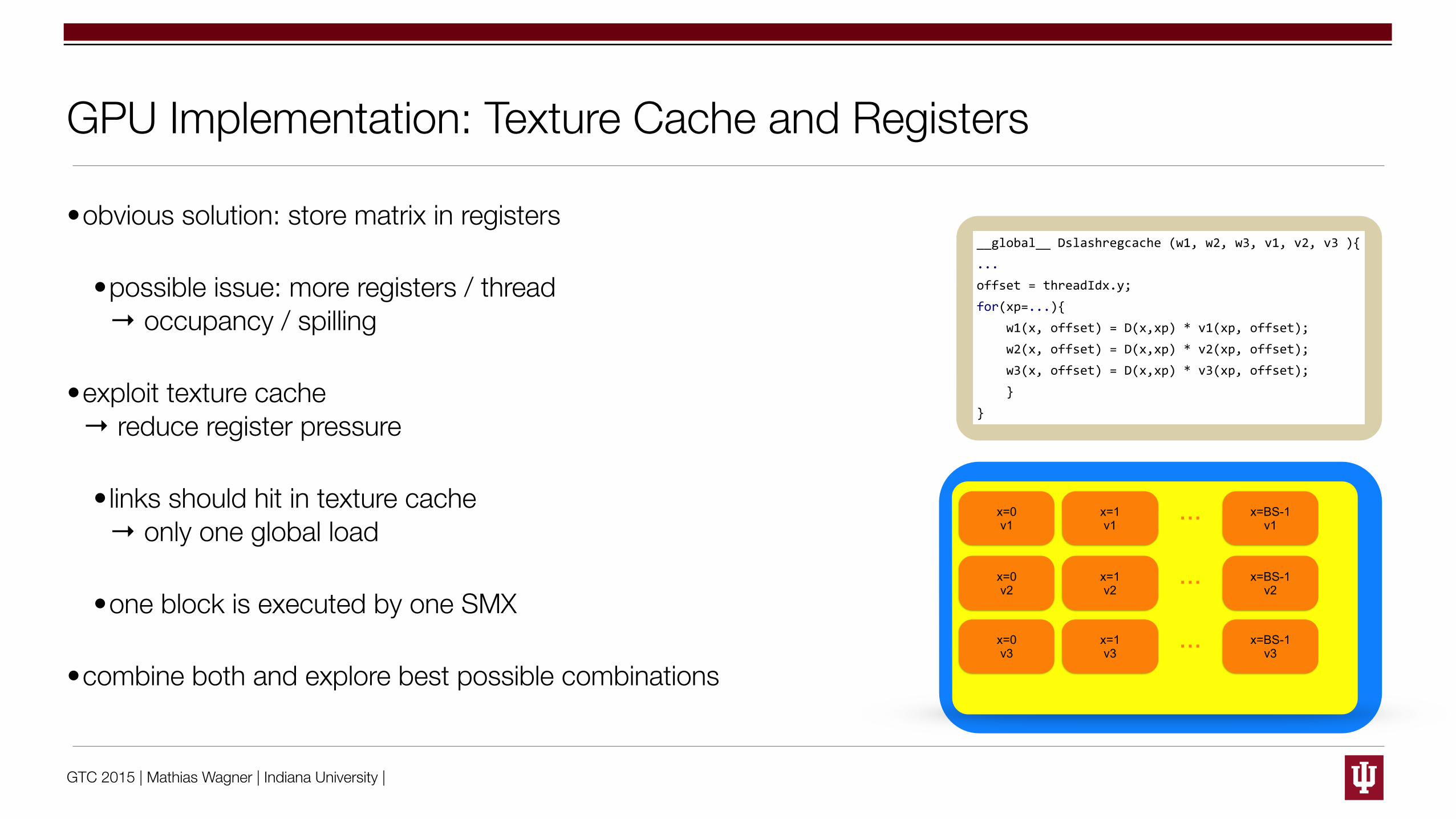
GTC 2015 | Mathias Wagner | Indiana University |
GPU Implementation: Texture Cache and Registers
•obvious solution: store matrix in registers
•possible issue: more registers / thread → occupancy / spilling
•exploit texture cache → reduce register pressure
•links should hit in texture cache → only one global load
•one block is executed by one SMX
•combine both and explore best possible combinations
__global__'Dslashreg'(w1,'w2,'w3,'v1,'v2,'v3'){...for(xp=...){' w1(x)'='D(x,xp)'*'v1(xp);' w2(x)'='D(x,xp)'*'v2(xp);' w3(x)'='D(x,xp)'*'v3(xp);'' }}
__global__'Dslashcache'(w,'v)...offset'='threadIdx.y;for(xp=...)' w(x,'offset)'+='D(x,xp)'*'v(x,'offset)}
__global__'Dslashregcache'(w1,'w2,'w3,'v1,'v2,'v3'){...offset'='threadIdx.y;for(xp=...){' w1(x,'offset)'='D(x,xp)'*'v1(xp,'offset);' w2(x,'offset)'='D(x,xp)'*'v2(xp,'offset);' w3(x,'offset)'='D(x,xp)'*'v3(xp,'offset);'' }}
x=0 v1
x=1 v1
x=BS-1 v1
x=0 v2
x=1 v2
x=BS-1 v2
x=0 v3
x=1 v3
x=BS-1 v3
�
�
�
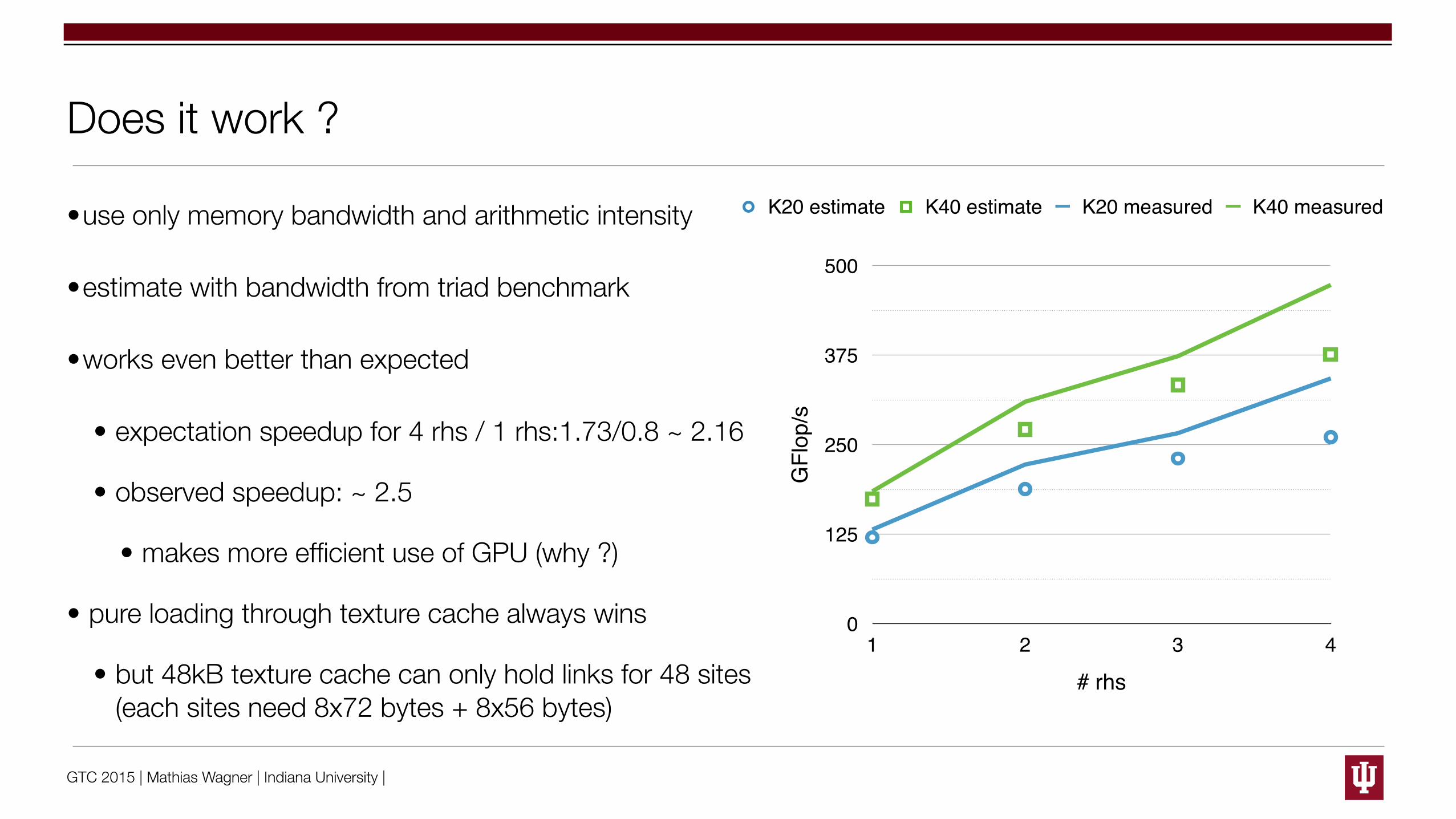
GTC 2015 | Mathias Wagner | Indiana University |
Does it work ?
•use only memory bandwidth and arithmetic intensity
•estimate with bandwidth from triad benchmark
•works even better than expected
• expectation speedup for 4 rhs / 1 rhs:1.73/0.8 ~ 2.16
• observed speedup: ~ 2.5
• makes more efficient use of GPU (why ?)
• pure loading through texture cache always wins
• but 48kB texture cache can only hold links for 48 sites (each sites need 8x72 bytes + 8x56 bytes)
GFl
op/s
0
125
250
375
500
# rhs1 2 3 4
K20 estimate K40 estimate K20 measured K40 measured
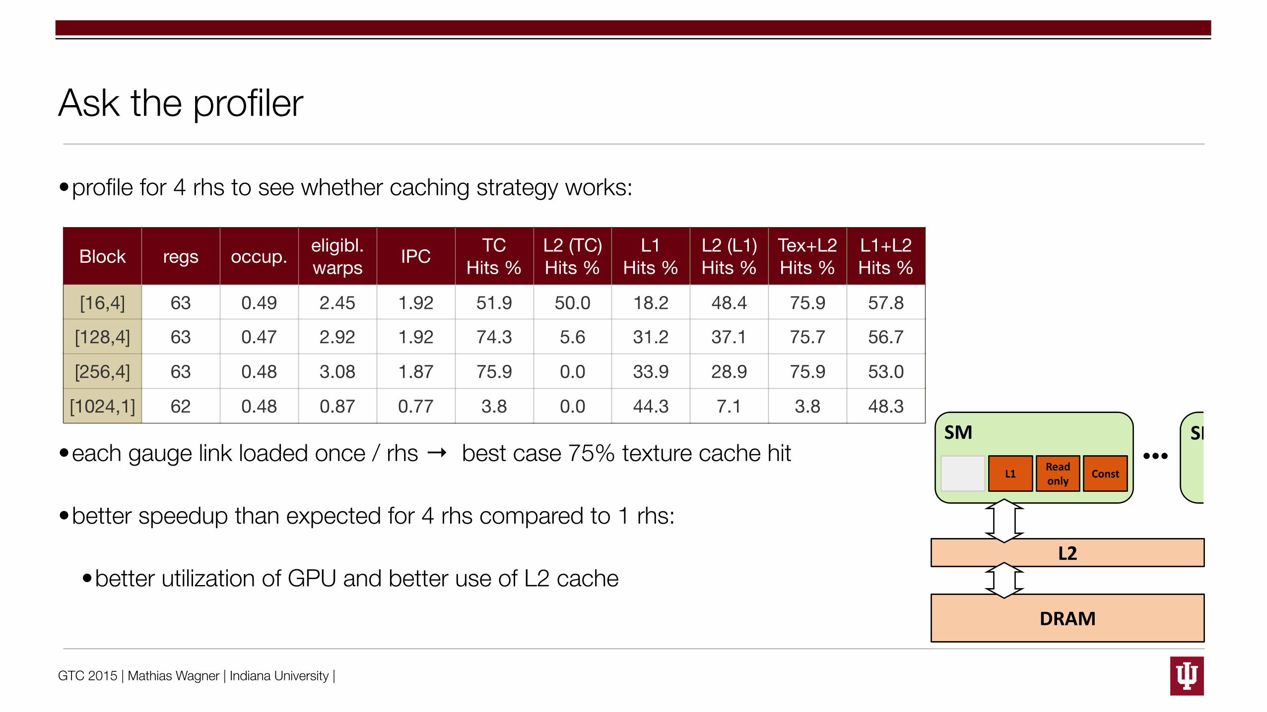
GTC 2015 | Mathias Wagner | Indiana University |
Ask the profiler
•profile for 4 rhs to see whether caching strategy works:
•each gauge link loaded once / rhs → best case 75% texture cache hit
•better speedup than expected for 4 rhs compared to 1 rhs:
•better utilization of GPU and better use of L2 cache
Block
[16,4]
[128,4]
[256,4]
[1024,1]
regs
63
63
63
62
occup.
0.49
0.47
0.48
0.48
eligibl. warps
2.45
2.92
3.08
0.87
IPC
1.92
1.92
1.87
0.77
TCHits %
51.9
74.3
75.9
3.8
L2 (TC)Hits %
50.0
5.6
0.0
0.0
L1Hits %
18.2
31.2
33.9
44.3
L2 (L1)Hits %
48.4
37.1
28.9
7.1
Tex+L2Hits %
75.9
75.7
75.9
3.8
L1+L2Hits %
57.8
56.7
53.0
48.3
GPU Memory System
© 2013, NVIDIA 36
DRAM
L2
SM
L1 Read only
Const
SM • Once in an SM, data goes into one of 3 caches/buffers
• Programmer’s choice – L1 is the “default”
– Read-only, Const require explicit code

GTC 2015 | Mathias Wagner | Indiana University |
Can we understand why it works ?
•focus on pure texture cache solution [1,4]
•each thread needs (8 x 72 + 8 x 56)=1024 bytes
•warps (32 threads) assigned to one scheduler
4 x 12 kB Texture / read only cacheSchedulerSchedulerSchedulerScheduler
Cache Cache Cache Cache

GTC 2015 | Mathias Wagner | Indiana University |
Can we understand why it works ?
•focus on pure texture cache solution [1,4]
•each thread needs (8 x 72 + 8 x 56)=1024 bytes
•warps (32 threads) assigned to one scheduler
•switching between threads: need only some of the data
•block sizes and warps
•[16,4] → 2 warps
•[128,4] → 16 warps
Tex Cache Tex Cache Tex Cache Tex Cache
(0…15,0) (0…15,1)
(0…15,2) (0…15,3)
(16…31,0) (16…31,1)
(16…31,2) (16…31,3)
Block TCHits %
L2 (TC)Hits %
Tex+L2Hits %
[16,4] 51.9 50.0 75.9
[128,4] 74.3 5.6 75.7

GTC 2015 | Mathias Wagner | Indiana University |
Can we understand why it works ?
•focus on pure texture cache solution [1,4]
•each thread needs (8 x 72 + 8 x 56)=1024 bytes
•warps (32 threads) assigned to one scheduler
•switching between threads: need only some of the data
•block sizes and warps
•[16,4] → 2 warps
•[128,4] → 16 warps
Tex Cache Tex Cache Tex Cache Tex Cache
(64…95,1)(32…64,1)(0…31,1) (96…127,1)
(64…95,0)(32…64,0)(0…31,0) (96…127,0)
(64…95,2)(32…64,2)(0…31,2) (96…127,2)
(64…95,3)(32…64,3)(0…31,3) (96…127,3)
Block TCHits %
L2 (TC)Hits %
Tex+L2Hits %
[16,4] 51.9 50.0 75.9
[128,4] 74.3 5.6 75.7

GTC 2015 | Mathias Wagner | Indiana University |
Some Details of the Phi Implementation
•effort lead by Patrick Steinbrecher (Universität Bielefeld → Brookhaven National Lab)
•single accelerator
•optimized for performance with multiple rhs
•parallelized using OpenMP
•vectorized using intrinsics:
•fuse lattice sites into 512bit vectors
•16 sites with SoA-layout
naive 16-fold site fusion
( ),,,
,,, ⇥
16 matrices times
16 vectors
|
{z
}
sites
( )
real imag
matrix
vector

GTC 2015 | Mathias Wagner | Indiana University |
Impact of Memory Layout and Prefetch
•register pressure limits scaling with #rhs
•software prefetching improves by about 2x
•hardware prefetching not effective for access pattern
•8-fold site fusion
•reduces register pressure
•harder to implement
•small gain for 1 rhs
Gflo
p/s
0
75
150
225
300
# rhs1 2 3 4 5
16-fold 16-fold + prefetch8-fold 8-fold + prefetch

GTC 2015 | Mathias Wagner | Indiana University |
Let’s get ready to rumble
Results for the full conjugate gradient inverter on Xeon Phi and Tesla
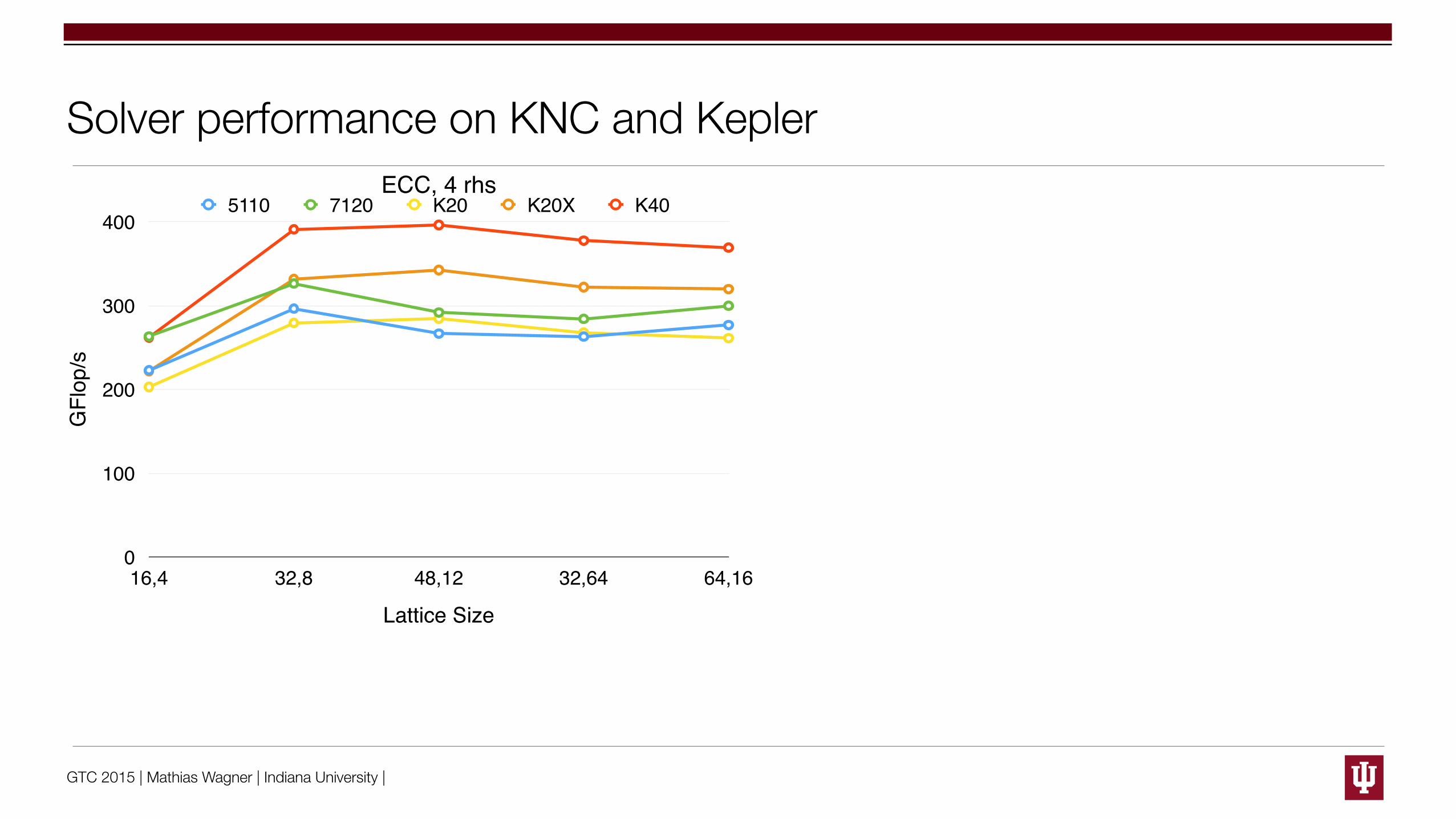
GTC 2015 | Mathias Wagner | Indiana University |
Solver performance on KNC and KeplerECC, 4 rhs
GFl
op/s
0
100
200
300
400
Lattice Size16,4 32,8 48,12 32,64 64,16
5110 7120 K20 K20X K40

GTC 2015 | Mathias Wagner | Indiana University |
Solver performance on KNC and KeplerECC, 4 rhs
GFl
op/s
0
100
200
300
400
Lattice Size16,4 32,8 48,12 32,64 64,16
5110 7120 K20 K20X K40
64^3 x 16, ECC
GFl
op/s
0
100
200
300
400
# rhs1 2 3 4 5
5110 7120 K20 K20X K40

GTC 2015 | Mathias Wagner | Indiana University |
Solver performance on KNC and KeplerECC, 4 rhs
GFl
op/s
0
100
200
300
400
Lattice Size16,4 32,8 48,12 32,64 64,16
5110 7120 K20 K20X K40
64^3 x 16, ECC
GFl
op/s
0
100
200
300
400
# rhs1 2 3 4 5
5110 7120 K20 K20X K40
performance relative to K20, 4 rhs
0.00
0.43
0.85
1.28
1.70
5110 7120 K20 K40
peak bw triad bw 32^3x8 CG 64^3x16 CG

GTC 2015 | Mathias Wagner | Indiana University |
Green or blue computing
How energy efficient are the two architectures?
Oh, does anyone wonder about Maxwell in this respect?

GTC 2015 | Mathias Wagner | Indiana University |
Energy consumption
•bandwidth-bound applications are unlikely to hit TDP
•What is the relevant observable?
•energy consumed by the node?
•energy consumed by the accelerator?
•include infrastructure (cooling, …) ?
•Take what we can get
•software reported power consumption (nvprof)
•Xeon Phi is a bit more tricky: estimate only
Solver, 4rhs, 32x8
Solve
r avg
. Pow
er [W
]
0
50
100
150
200
250
5110 (est) K20 K40 M6000
TDP CG ECC CG noECC

GTC 2015 | Mathias Wagner | Indiana University |
Performance per Watt So
lver [
GFl
op/s
]
0
120
240
360
480
600
CG ECC CG noECC
5110 (est) K20 K40 M6000
[GFl
op/s
/ W
]
0
0.6
1.2
1.8
2.4
3
CG ECC CG noECC
5110 (est) K20 K40 M6000
•Solver 4 rhs, 323 x 8preliminary: code only optimized for Kepler

GTC 2015 | Mathias Wagner | Indiana University |
Finish

GTC 2015 | Mathias Wagner | Indiana University |
Summary
•Lattice QCD applications reflects triad bandwidth
•equally well performing implementations for GPU / Phi
•multiple rhs achieve can easily speedup solver by 2.5
•Xeon Phi requires vectorization and software prefetches
•GPU uses texture cache
•Caching of vectors likely improved with multiple rhs
performance relative to K20, 4 rhs
0.00
0.50
1.00
1.50
2.00
5110 7120 K20 K40
peak bw triad bw32^3x8 CG 64^3x16 CG
[GFl
op/s
/ W
]
00.61.21.82.4
3
5110 (est) K20 K40 M6000
•GK110 about 1.5 times more efficient than KNC
•Maxwell promises another factor 1.5
•multiple rhs about twice as energy efficient

GTC 2015 | Mathias Wagner | Indiana University |
GPU vs Xeon Phi:Performance of Bandwidth Bound Applications with a Lattice QCD Case Study
Contact: [email protected] http://linked.in/mathwagn @mathwagn
Collaborators: P. Steinbrecher (Bielefeld U → Brookhaven National Lab) C. Schmidt (Bielefeld U) O. Kaczmarek (Bielefeld U)
References: arXiv:1411.4439 [physics.comp-ph] arXiv:1409.1510 [cs.DC]
Thanks to: Jeongnim Kim (Intel)Mike Clark (Nvidia)