Government Girls’ Polytechnic, Bilaspur Name of the Lab ...
50
Network Analysis Lab Manual:3 rd semester(ET&T) 1 Government Girls’ Polytechnic, Bilaspur Name of the Lab:Electrical&Electronic Measurement Lab Practical: Network Analysis Lab Class :3 rd Semester ( ET&T ) Teachers Assessment: 10 End Semester Examination: 50 EXPERIMENT No- 1 OBJECTIVE: - Apply the kickoffs law for finding current in a complex electrical circuit EQUIPMENT REQUIRED: - Batteries, Resistors, Multimeter,Battery Holders,Connecting Leads, Alligator clips.. THEORY:- KCL:- This law is also called Kirchhoff's point rule, Kirchhoff's junction rule (or nodal rule), and Kirchhoff's first rule. Kirchoff's first law states that: ―the sum of the currents flowing through a node must be zero‖. This law is particularly useful when applied at a position where the current is split into pieces by several wires. The point in the circuit where the current splits is known as a node. Or ―The algebraic sum of current at any node of a circuit is zero‖. The direction of incoming currents to a node being positive the outgoing current should be taken negative. n is the total number of branches with currents flowing towards or away from the node. PROCEDURE :- For Current Law:- 1. Using the multimeter, measure the value of the resistance of each of the three resistors provided by setting the scale of the multimeter on the 200K scale. 2. Use the multimeter to measure the voltage from the battery(s) in the single D battery holders and the two D battery holder. 3. Set up the circuit shown in Figure . In this circuit, use one of the single D battery holder for VB1a and the two D battery holder for VB2. For the resistors in the circuit, use the resistors closest to the following values: R1 = 50 k ohm, R2 = 20k ohm, and R3 = 10 k ohm 4. Set the multimeter on 200 u on the current scale (i.e. `the `A" scale). Attach a black lead to the COM terminal and a red lead to the mA terminal. With these settings, the multimeter is set to read the current in the circuit in micro Amperes (i.e. ¹A).
Transcript of Government Girls’ Polytechnic, Bilaspur Name of the Lab ...

Network Analysis Lab Manual3rd
semester(ETampT) 1
Government Girlsrsquo Polytechnic
Bilaspur Name of the LabElectricalampElectronic Measurement Lab
Practical Network Analysis Lab Class 3rd Semester ( ETampT )
Teachers Assessment 10 End Semester Examination 50
EXPERIMENT No- 1
OBJECTIVE - Apply the kickoffs law for finding current in a complex electrical circuit EQUIPMENT REQUIRED - Batteries Resistors MultimeterBattery HoldersConnecting Leads Alligator clips THEORY- KCL- This law is also called Kirchhoffs point rule Kirchhoffs junction rule (or nodal rule) and Kirchhoffs first rule Kirchoffs first law states that ―the sum of the currents flowing through a node must be zero This law is particularly useful when applied at a position where the current is split into pieces by several wires The point in the circuit where the current splits is known as a node Or ―The algebraic sum of current at any node of a circuit is zero The direction of incoming currents to a node being positive the outgoing current should be taken negative
n is the total number of branches with currents flowing towards or away from the node
PROCEDURE - For Current Law-
1 Using the multimeter measure the value of the resistance of each of the three resistors provided by setting the scale of the multimeter on the 200K scale 2 Use the multimeter to measure the voltage from the battery(s) in the single D battery holders and the two D battery holder 3 Set up the circuit shown in Figure In this circuit use one of the single D battery holder for VB1a and the two D battery holder for VB2 For the resistors in the circuit use the resistors closest to the following values R1 = 50 k ohm R2 = 20k ohm and R3 = 10 k ohm 4 Set the multimeter on 200 u on the current scale (ie `the `A scale) Attach a black lead to the COM terminal and a red lead to the mA terminal With these settings the multimeter is set to read the current in the circuit in micro Amperes (ie sup1A)
Network Analysis Lab Manual3rd
semester(ETampT) 2
5 Measure the current flowing into the top node of the circuit from each of the three branch wires To measure the current you will have to break the circuit to insert the multimeter You must also measure the polarity of the current in a consistent manner If the current flows into the node then the current should be measured from the positive (redmA) terminal to the negative (blackCOM) terminal Record these measured currents on your data table 6 In the space provided on the data table add the three currents to check that the sum of the currents is zero (or close to zero)
For KVL 1) Connect the circuit as per the circuit diagram on bread board supply using connecting wire sand chords 2) Switch on the power supply and adjust V1 and V2 3) Measure VR1 amp VR2 VR3 VR4 amp VR5 4) Select any desired loop say loop (1) apply KVL as per given in observation table and verify the result 5) Repeat step (2) onwards for different V1 and V2
OBSERVATION - For CurrentNode Law-
(a) Current across individual resistor R1 R2 amp R3 (I= VR)
I1 = -------
I2 = ------
I3 = ------
(b) Verifying KCL using measured values I1 + I2 + I3 = -------- For Kirchoffs Voltage Law Starting from point A if we go around the mesh in clockwise direction the different EMFrsquo s amp IOR drop will have following values and signs I1R1 ------ is ndashve ( fall in potential ) I2R2 ----- - is +ve (rise in potential ) E2 ------ is ndashve ( fall in potential I 3R3 ------ is ndashve ( fall in potential ) E1--------- is +ve ( rise in potential )
I 4R4--------- is ndashve ( fall in potential )
Network Analysis Lab Manual3rd
semester(ETampT) 3
According to KVL I 1R1 ndash I 2R2 ndash E2 - I 3R3 + E1 ndash I 4R4 = 0 - I1R1 + I2R2 - I3R3 - I4R4 = E2 - E1 I1R1- I2R2 + I3R3 + I4R4 = E1- E2
VR1- VR2 + VR3 + VR4 = E1- E2 Determination of algebraic sign 1 Battery EMF While going round a loop ( in a direction of our own choice ) if we go from the -ve terminal of battery to its +ve terminal there is rise in potential hence this EMF should be given as + ve signal On the other hand if we go from its + ve terminal its -ve terminal therersquos a fall in potential hence this battery EMF should be given as -ve sign 2 IR drops in series If we go through a circuit in the same direction as its current then there is a fall or decrease in potential for the simple reason that current always flow from higher to lower potential Hence this IR drop should be taken as -ve However if we go around the loop in direction opposite to that of the current there is a rise in voltage Hence these IR should be taken as +ve It clears that the algebraic sign of IR drop
across a resister depends on the direction of current through that resistor
observation table
for KCL
S No
V1
V2
I1
I2
I3
I3 = I1+I2
Network Analysis Lab Manual3rd
semester(ETampT) 4
1
2
For KVL
S No
V1
V2
VR1
VR2
VR3
VR4
VR5
V1=VR1+VR2+VR5
V2=VR3+VR4+VR5
1
2
RESULT- The current approaching to the junction is equal to currents leaving from the junction So KCL is verified similarly voltage supplied to desired loop equals to voltage drop by same loop so KVL is verified
PRECAUTIONS - 1) All the connection should be tight 2) Ammeter is always connected in series in the circuit while voltmeter is parallel to the conductor 3) The electrical current should not flow the circuit for long time Otherwise its temperature will increase and the result will be affected 4) It should be care that the values of the components of the circuit is does not exceed to their ratings (maximum value) 5) Before the circuit connection it should be check out working condition of all the Component
Network Analysis Lab Manual3rd
semester(ETampT) 5
EXPERIMENT No- 2
Objective - Apply the thieving theorem for finding current in a complex electrical circuit
Theory
Theacutevenins theorem-
In circuit theory Theacutevenins theorem for linear electrical networks states that any combination of voltage sources current sources and resistors with two terminals is electrically equivalent to a single voltage source V and a single series resistor R For single frequency AC systems the theorem can also be applied to general impedances not just resistors The theorem was first discovered by German scientist Hermann von Helmholtz in 1853
[1] but was then rediscovered in 1883 by French telegraph engineer
Leacuteon Charles Theacutevenin (1857ndash1926)
This theorem states that a circuit of voltage sources and resistors can be converted into a Theacutevenin equivalent which is a simplification technique used in circuit analysis The Theacutevenin equivalent can be used as a good model for a power supply or battery (with the resistor representing the internal impedance and the source representing the electromotive force) The circuit consists of an ideal voltage source in series with an ideal resistor
Any black box containing only voltage sources current sources and other resistors can be converted to a Theacutevenin equivalent circuit comprising exactly one voltage source and one resistor
Calculating the Theacutevenin equivalent
To calculate the equivalent circuit the resistance and voltage are needed so two equations are required These two equations are usually obtained by using the following steps but any conditions placed on the terminals of the circuit should also work
1 Calculate the output voltage VAB when in open circuit condition (no load resistormdashmeaning infinite resistance) This is VTh
2 Calculate the output current IAB when the output terminals are short circuited (load resistance is 0) RTh equals VTh divided by this IAB
The equivalent circuit is a voltage source with voltage VTh in series with a resistance RTh
Network Analysis Lab Manual3rd
semester(ETampT) 6
Step 2 could also be thought of as
2a Replace voltage sources with short circuits and current sources with open circuits 2b Calculate the resistance between terminals A and B This is RTh
The Theacutevenin-equivalent voltage is the voltage at the output terminals of the original circuit When calculating a Theacutevenin-equivalent voltage the voltage divider principle is often useful by declaring one terminal to be Vout and the other terminal to be at the ground point
The Theacutevenin-equivalent resistance is the resistance measured across points A and B looking back into the circuit It is important to first replace all voltage- and current-sources with their internal resistances For an ideal voltage source this means replace the voltage source with a short circuit For an ideal current source this means replace the current source with an open circuit Resistance can then be calculated across the terminals using the formulae for series and parallel circuits This method is valid only for circuits with independent sources If there are dependent sources in the circuit another method must be used such as connecting a test source across A and B and calculating the voltage across or current through the test source
Example
Step 0 The original circuit
Network Analysis Lab Manual3rd
semester(ETampT) 7
Step 1 Calculating the equivalent output voltage
Step 2 Calculating the equivalent resistance
Step 3 The equivalent circuit
In the example calculating the equivalent voltage
Vth=[R2+R3(R2+R3=R4)]V1
Vth=[1k Ω +1 k Ω (1 k Ω +1 k Ω +2 k Ω)] 15V
= frac12(15) = 75V
Network Analysis Lab Manual3rd
semester(ETampT) 8
(notice that R1 is not taken into consideration as above calculations are done in an open circuit condition between A and B therefore no current flows through this part which means there is no current through R1 and therefore no voltage drop along this part)
Calculating equivalent resistance
Rth = R1+[(R2+R3)||R4]
= 1 k Ω +[(1 k Ω +1 k Ω )||2 k Ω]
=2 k Ω
Conversion to a Norton equivalent
A Norton equivalent circuit is related to the Theacutevenin equivalent by the following
Rth=Rno
Vth=Ino Rno
Ino=VthRth
Practical limitations
Many if not most circuits are only linear over a certain range of values thus the Theacutevenin equivalent is valid only within this linear range and may not be valid outside the range
The Theacutevenin equivalent has an equivalent I-V characteristic only from the point of view of the load
The power dissipation of the Theacutevenin equivalent is not necessarily identical to the power dissipation of the real system However the power dissipated by an external resistor between the two output terminals is the same however the internal circuit is represented
PRECAUTIONS - 1) All the connection should be tight
2) It should be care that the values of the components of the circuit is does not exceed to their ratings (maximum value)
3) Before the circuit connection it should be check out working condition of all the Component
Network Analysis Lab Manual3rd
semester(ETampT) 9
Experiment no 3
Aim - Verify the Nortonrsquos theorem
Theory
EQUIPMENT REQUIRED 1Power supply 2 Resistors3 Connecting wires4 Bread board Multimetersammeter
Statement - Nortons theorem for linear electrical networks states that any collection of voltage sources current sources and resistors with two terminals is electrically equivalent to an ideal current source I in parallel with a single resistor R
For single-frequency AC systems the theorem can also be applied to general impedances not just resistors The Norton equivalent is used to represent any network of linear sources and impedances at a given frequency The circuit consists of an ideal current source in parallel with an ideal impedance (or resistor for non-reactive circuits)
Calculation of a Norton equivalent circuit
The Norton equivalent circuit is a current source with current INo in parallel with a resistance RNo To find the equivalent
1 Find the Norton current INo Calculate the output current IAB with a short circuit as the load (meaning 0 resistances between A and B) This is INo
2 Find the Norton resistance RNo When there are no dependent sources (ie all current and voltage sources are independent) there are two methods of determining the Norton impedance RNo
Calculate the output voltage VAB when in open circuit condition (ie no load resistor mdash meaning infinite load resistance) RNo equals this VAB divided by INo OR Replace independent voltage sources with short circuits and independent current sources with open circuits The total resistance across the output port is the Norton impedance RNo
Any collection of batteries and resistances with two terminals is electrically equivalent to an ideal current source i in parallel with a single resistor r The value of r is the same as that in the Thevenin equivalent and the current i can be found by dividing the open circuit voltage by r
Norton Current
Network Analysis Lab Manual3rd
semester(ETampT) 10
The value i for the current used in Nortons Theorem is found by determining the open circuit voltage at the terminals AB and dividing it by the Norton resistance r
Norton Example
Replacing a network by its Norton equivalent can simplify the analysis of a complex circuit In this example the Norton current is obtained from the open circuit voltage (the Thevenin voltage) divided by the resistance r This resistance is the same as the Thevenin resistance the resistance
Network Analysis Lab Manual3rd
semester(ETampT) 11
looking back from AB with V1 replaced by a short circuit
For R1 = hellip Ω
R2 =hellip Ω
R3 =helliphellip Ω
And voltage V1 =helliphellip V
The open circuit voltage is = = helliphellipV
Since R1 and R3 form a simple voltage divider
The Norton resistance is = = helliphellip Ω
and the resulting Norton current is = = helliphellipA
Network Analysis Lab Manual3rd
semester(ETampT) 12
circuit diagram
Observation table-
Result- Norton theorem is verified
PRECAUTIONS - 1) All the connection should be tight
2) It should be care that the values of the components of the circuit is does not exceed to their ratings (maximum value)
4) Before the circuit connection it should be check out working condition of all the Component
Network Analysis Lab Manual3rd
semester(ETampT) 13
Experiment no ndash 4
Objective ndash Verify the theorems
a Super position theorems
b Maximum power transfer theorem force circuits
Apparatus required ndash 1power supply2 Variable resistors3 Connecting wires4 Bread board5 Multimetersammeter Theory - The maximum power transfer theorem states that a load resistance will abstract maximum power from the network when the load resistance is equal to the internal resistance For maximum power transfer Load resistance RL=Rth Where Rth equivalent resistance of the remaining circuit Maximum power = P max =V24RL Where V is the dc supply voltage Circuit diagram -
PROCEDURE 1 Connect the circuit diagram as shown in fig 2 Take the readings of voltmeter and ammeter for different values of RL 3 Verify that power is maximum when RL =RI
Network Analysis Lab Manual3rd
semester(ETampT) 14
OBSERVATION TABLE
RESULT Maximum power transfer theorem has been verified Superposition theorem Apparatus required ndash 2mm Patch cords2) Digital Multimeter3) Superposition Theorem Kit Statement- In a linear bilateral active network containing more than one source of emf current the current flowing through any branch point is the algebraic sum of all the currents flowing through that branch point considering that a single source of emf current is in acting at a time while all the other sources of emf current are replaced by their internal resistances (for the time being) EXPLANATION1 Select only one source and replace all other sources by there internal resistances (If the source is the ideal currentsource replace it by open ckt if the source is the ideal voltage source replaces it by short ckt)2 Find the current and its direction through the desired branch3 Add all the branch currents to obtain the actual branch current Circuit diagram
STEPWISE PROCEDURE
Network Analysis Lab Manual3rd
semester(ETampT) 15
1 Make the connections as per the circuit diagram 2 Keep both Switches S1 and S2 at position 1 3 Switch ON both the DC sources 4 Adjust the Rheostats such that the ammeter will read properly 5 Note down the value of current from ammeter A as I amp 6 Switch OFF the sources 7 Keep the Switch S1 at position 1 and S2 at position 2 then Switch ON the supply source E1 only 8 Note down the value of current from Ammeter as I amp 9 Switch OFF the supply and Keep the Switch S1 at position 2 Switch S2 at position 1 10 Switch ON the supply source E2 only 11 Note down the value of current from Ammeter as I 12 Switch OFF the supply 13 Adjust the values of Rheostats and repeat the above procedure 14 Note down two more sets of readings 15 Switch OFF the supply and disconnect the circuit OBSERVATIONS table
CALCULATIONS Calculate branch current I = I + I for each reading and tabulate the result RESULT Superposition theorem has been verified
PRECAUTIONS - 1) All the connection should be tight
2) It should be care that the values of the components of the circuit is does not exceed to their ratings (maximum value)
5) Before the circuit connection it should be check out working condition of all the Component
Network Analysis Lab Manual3rd
semester(ETampT) 16
Experiment no 5
Objective- Observe the wave shape of an integrating ckt on the CRO
Apparatus required Four 6 volt batteriesOperational amplifier model 1458 recommended (Radio Shack catalog 276-038)One 10 kΩ potentiometer linear taper (Radio Shack catalog 271-1715)Two capacitors 01 microF each non-polarized (Radio Shack catalog 272-135)Two 100 kΩ resistorsThree 1 MΩ resistors
Theory- Connect a voltmeter between the op-amps output terminal and the circuit ground point Slowly move the potentiometer control while monitoring the output voltage The output voltage should be changing at a rate established by the potentiometers deviation from zero (center) position To use calculus terms we would say that the output voltage represents the integral (with respect to time) of the input voltage function That is the input voltage level establishes the output voltage rate of change over time This is precisely the opposite of differentiation where the derivative of a signal or function is its instantaneous rate of changeIf you have two voltmeters you may readily see this relationship between input voltage and output voltage rate of change by measuring the wiper voltage (between the potentiometer wiper and ground) with one meter and the output voltage (between the op-amp output terminal and ground) with the other Adjusting the potentiometer to give zero volts should result in the slowest output voltage rate-of-change Conversely the more voltage input to this circuit the faster its output voltage will change or ramp
Circuit diagram ndash
Network Analysis Lab Manual3rd
semester(ETampT) 17
As soon as the grounding resistor is shorted with a jumper wire the op-amps output voltage will start to change or drift Ideally this should not happen because the integrator circuit still has an input signal of zero volts However real operational amplifiers have a very small amount of current entering each input terminal called the bias current These bias currents will drop voltage across any resistance in their path Since the 1 MΩ input resistor conducts some amount of bias current regardless of input signal magnitude it will drop voltage across its terminals due to bias current thus offsetting the amount of signal voltage seen at the inverting terminal of the op-amp If the other (noninverting) input is connected directly to ground as we have done here this offset voltage incurred by voltage drop generated by bias current will cause the integrator circuit to slowly integrate as though it were receiving a very small input signal Waveform
Network Analysis Lab Manual3rd
semester(ETampT) 18
Result - wave shape of an integrating ckt on the CRO is Observed
PRECAUTIONS - 1) All the connection should be tight
2) It should be care that the values of the components of the circuit is does not exceed to their ratings (maximum value)
6) Before the circuit connection it should be check out working condition of all the Component
Network Analysis Lab Manual3rd
semester(ETampT) 19
Experiment no 6
Objective- Observe the wave shape of a differentiating ckt
Apparatus required Resistors Capacitors Op-Amp IC 741 Connecting wires and CRO probes
Theory
DifferentiatorOne of the simplest of the op-amp circuits that contain capacitor is theDifferentiating Amplifier or Differentiator As the name suggests the circuit performsthe mathematical operation of differentiation that is the output waveform is thederivative of input waveform A differentiator circuit is shown in figThe node N is at virtual ground potential ie Vn = 0 The current iC the capacitor isiC = C1 ddt (Vi - Vn) = C1 dVidt ---------------(1)The current if through the feedback resistor is VoRf and there is no current into the opampTherefore the nodal equation at node N is
C1( dVidt) + VoVf = 0 From which we have Vo = - Rf C1 (dVidt )------------------(2) Thus the output voltage Vo is a constant (-RfC1) times the derivative of the input voltage Vi and the circuit is a differentiator The sign indicates a 180o phase shift of the output waveform V0 with respect to the input signal The phasor equivalent of Eq (2) is Vo(s) = - RfC1 s Vi(s) where Vo and Vi is the phasor representation of Vo and Vi In steady state put s = j_ We may now write the magnitude of gain A of the differentiator as A = VoVi = - j_ Rf C1 = _ Rf C1 ----------------(3) From Eq (3) one can draw the frequency response of the op-amp differentiator Equation (3) may be rewritten as A = f fa Where fa = 12_ Rf C1
f=operating frequency
CIRCUIT DIAGRAM
Network Analysis Lab Manual3rd
semester(ETampT) 20
Fig Differentiator Waveform
Network Analysis Lab Manual3rd
semester(ETampT) 21
Fig Input amp Output waveforms Result- wave shape of a differentiating ckt is Observed
PRECAUTIONS - 1) All the connection should be tight
2) It should be care that the values of the components of the circuit is does not exceed to their ratings (maximum value)
7) Before the circuit connection it should be check out working condition of all
the Component
Network Analysis Lab Manual3rd
semester(ETampT) 22
Experiment no 7
Objective- Use the filter circuit in musical light system
Theory - Play a song from your audio source and probe the signal with your oscilloscope Adjust the horizontal and vertical scales so you can see several seconds of the signal at once The energy of a bass drum lies mainly in frequencies under 200Hz To isolate the bass drum we need to eliminate the songrsquos high frequencies with a low pass filter The ideal low pass filter has the magnitude response shown in Figure 2(a) where all frequencies below the cutoff are passed through untouched and all frequencies above the cutoff are blocked completely This magnitude response is impossible in reality but you will implement one of the filters shown in Figure 2(b) as an approximation When you design your low pass filter you will be faced with many important choices As an engineer you must guide your decisions by considering the cost and effectiveness of each implementation
1Effectiveness The filter must attenuate the high frequencies so the LED blinks
only in response to the bass drum and not any other instruments 2Cost The filter must be as simple as possible (but still be effective) We could use a monstrous 10th order filter but that is far more complicated than necessary In the real world higher complexity translates to higher cost
1
Network Analysis Lab Manual3rd
semester(ETampT) 23
Connection diagram Figure
Block diagram of the circuit
Waveform
Network Analysis Lab Manual3rd
semester(ETampT) 24
Example filter magnitude response and general terminology The passband and stopband are the ranges of frequency that are nominally passed through and blocked by the filter The cutoff frequency separates them Stopband attenuation is the minimum attenuation of all stopband frequencies Roll-off is how quickly stopband frequencies are attenuated as frequency increases Ripple is how much the magnitude response ripples in passband or stopband 1 Bessel The Bessel filter has the slowest roll-off of all 5 filters Its chief advantage is its maximally flat group delay in the passband Group delay is simply the derivative of the phase response (both are plotted vs frequency) It is a measure of the time it takes for a signal to pass through a filter Group delay increases with increasing filter order and decreasing cutoff frequency which is bad We do not want the LED to blink AFTER we hear the beat we want the blink and the beat to coincide or be so close together we cannot perceive the delay The Besselrsquos flat group delay means all frequencies in the passband are delayed the same amount which means there is no signal distortion at the output due to different frequencies being delayed different amounts The filter parameters stopband attenuation and ripple have no effect on this filter
2 Butterworth The Butterworth filter is the easiest of the 5 topologies to implement in analog circuits Its magnitude response is characterized by a maximally flat passband -3dB attenuation at the cutoff frequency and a roll-off of ndash20N dBdecade beyond cutoff where N is the order This roll-off is the slowest with the exception of the Bessel filter Stopband attenuation and ripple have no effect on the Butterworth
3 ChebyshevInverse Chebyshev These filters roll off more steeply than the Butterworth but exhibit ripple in passband (Chebyshev) or stopband (Inverse) The value of stopband attenuation has no effect on the Chebyshev filter ripple has no effect on the Inverse Chebyshev
3 Elliptic The elliptic filter rolls off more steeply than all other filters but exhibits ripple in both passband and stopband
Network Analysis Lab Manual3rd
semester(ETampT) 25
low pass filter schematic
The timer The final step is to set the length of each blink Without the timer the length of a blink is how long the peak from the peak detector signal stays above the threshold voltage This time differs from beat to beat We want to make this time the same for all beats We can do this with the monostable timer circuit from Figure
Network Analysis Lab Manual3rd
semester(ETampT) 26
Figure 9 The monostable timer circuit Recall that OUT is +Vcc when INltVcc3 ie OUT goes high when IN goes low OUT remains high until C1 initially with zero voltage across its terminals charges to (23)Vcc The time it takes for C1 to charge to (23)Vcc is tpulse = ln(3)R1C1 Pick values for tpulse R1 and C1 and write them down The comparator signal goes high on the beat but we need a trigger signal that goes low on the beat How can we produce this trigger signal from the comparator output Simply switch the two comparator inputs Wire the LED and the 100Ω resistor to the output of the timer and play your song Result - filter circuit is used in musical light system
PRECAUTIONS - 1) All the connection should be tight 2)It should be care that the values of the components of the circuit is does not exceed to their ratings (maximum value)
3) Before the circuit connection it should be check out working condition of all the Component
Network Analysis Lab Manual3rd
semester(ETampT) 27
Experiment no 8
Objective- Develop a ckt for simple project based on NW analysis Theory - This section deals with the resource aspects of network analysis and shows how resources of men machines etc could be scheduled over the project duration to be able to deal with resource andor time constraints Procedure for project Resources and Networks The usefulness of networks is not confined only to the time and cost factors which have been discussed so far Considerable assistance in planning and controlling the use of resources can be given to management by appropriate development of the basic network techniques Project resources The resources (men of varying skills machines of all types the required materials finance and space) used in a project are subject to varying demands and loadings as the project proceeds Management need to know what activities and what resources are critical to the project duration and if resource limitations (eg shortage of materials limited number of skilled personnel) might delay the project They also wish to ensure as far as possible constant work rates to eliminate paying overtime at one stage of a project and having short time working at another stage Resource Scheduling Requirements To be able to schedule the resource requirements for a project the following details are required a The customary activity times descriptions and sequences as previously
described b The resource requirements for each activity showing the classification of the
resource and the quantity required c The resources in each classification that are available to the project If variations
in availability are likely during the project life these must also be specified d Any management restrictions that need to be considered eg which activities may
or may not be split or any limitations on labour mobility Resources Scheduling Example Using a Gantt Chart A simple project has the following time and resource data (for simplicity only the one resource of labour is considered but similar principles would apply to other types of inter-changeable resources) Result ndashobjective is completed
Network Analysis Lab Manual3rd
semester(ETampT) 28
Experiment 9
Objective- Measurement of capacitance of a condenser without using RLC bridge
Theory - A capacitor is a common electronic circuit component that consists of two parallel plates separated by an insulating material called a dielectric When a battery with
voltage is connected across the capacitor equal and opposite charges rapidly collect onto the plates due to the electric field created by the wires connecting the two plates
1
Once the plates are fully charged one plate will have a net positive charge while the
other plate will have a net negative charge It has been shown empirically that the
charge on one of the plates is directly proportional to the applied potential
difference and the constant of proportionality is known as the capacitance2 The
amount of charge on each plate in this steady-state is then written as
(1)
where is in coulombs is in volts and is in farads (after 19th century British
physicists Michael Faraday) That is A one-farad capacitor is physically
quite large so it is more common to see capacitors in the picofarad ( ) to
microfarad ( ) range Since the capacitor charges in some finite amount of time the charge that exists on one of the plates at any time that is before a steady-state exists is given by
(2)
When capacitors are connected together in series and then connected to a battery as shown in Figure 1 the same amount of charge must build up on each of the capacitors It can be shown that the behavior of these capacitors is as if there was one single capacitor
with an effective capacitance given by the following
Capacitors in series
(3)
It should be readily seen that the effective capacitance of capacitors in series is smaller than the capacitance of any of the contributing elements However when capacitors are connected inparallel as shown in Figure 2 the effective capacitance is given by the sum of each capacitance or
Capacitors in parallel
(4)
Network Analysis Lab Manual3rd
semester(ETampT) 29
Result - capacitance of a condenser is Measured without using RLC bridge
PRECAUTIONS - 1) All the connection should be tight
2) It should be care that the values of the components of the circuit is does not exceed to their ratings (maximum value)
8) Before the circuit connection it should be check out working condition of all the Component
Network Analysis Lab Manual3rd
semester(ETampT) 30
Experiment no 10
Objective - Function of
c Low pass filter
d High pass filter
e Band pass filter
Apparatus required - Op- Amp 741 Resistances capacitor Function generator Theory
A low-pass filter is a filter that passes low-frequency signals but attenuates (reduces
the amplitude of) signals with frequencies higher than the cutoff frequency The actual
amount of attenuation for each frequency varies from filter to filter It is sometimes called
a high-cut filter ortreble cut filter when used in audio applications A low-pass filter is the
opposite of a high-pass filter and a band-pass filter is a combination of a low-pass and a
high-pass
Low-pass filters exist in many different forms including electronic circuits (such as a hiss
filter used in audio) digital filters for smoothing sets of data acoustic barriers blurring of
images and so on The moving average operation used in fields such as finance is a
particular kind of low-pass filter and can be analyzed with the same signal
processing techniques as are used for other low-pass filters Low-pass filters provide a
smoother form of a signal removing the short-term fluctuations and leaving the longer-
term trend
Ideal and real filters
The sinc function the impulse responseof an ideal low-pass filter
An ideal low-pass filter completely eliminates all frequencies above the cutoff
frequency while passing those below unchanged its frequency response is a rectangular
Network Analysis Lab Manual3rd
semester(ETampT) 31
function and is a brick-wall filter The transition region present in practical filters does not
exist in an ideal filter An ideal low-pass filter can be realized mathematically
(theoretically) by multiplying a signal by the rectangular function in the frequency domain
or equivalently convolution with its impulse response a sinc function in the time
domain
However the ideal filter is impossible to realize without also having signals of infinite
extent in time and so generally needs to be approximated for real ongoing signals
because the sinc functions support region extends to all past and future times The filter
would therefore need to have infinite delay or knowledge of the infinite future and past in
order to perform the convolution It is effectively realizable for pre-recorded digital signals
by assuming extensions of zero into the past and future or more typically by making the
signal repetitive and using Fourier analysis
Real filters for real-time applications approximate the ideal filter by truncating
and windowing the infinite impulse response to make a finite impulse response applying
that filter requires delaying the signal for a moderate period of time allowing the
computation to see a little bit into the future This delay is manifested as phase shift
Greater accuracy in approximation requires a longer delay
An ideal low-pass filter results in ringing artifacts via the Gibbs phenomenon These can
be reduced or worsened by choice of windowing function and the design and choice of
real filters involves understanding and minimizing these artifacts For example simple
truncation [of sinc] causes severe ringing artifacts in signal reconstruction and to
reduce these artifacts one uses window functions which drop off more smoothly at the
edges[2]
The WhittakerndashShannon interpolation formula describes how to use a perfect low-pass
filter to reconstruct a continuous signal from a sampleddigital signal Real digital-to-
analog converters use real filter approximations
Function of filters
Network Analysis Lab Manual3rd
semester(ETampT) 32
There are many different types of filter circuits with different responses to changing
frequency The frequency response of a filter is generally represented using a Bode plot
and the filter is characterized by its cutoff frequency and rate of frequency rolloff In all
cases at the cutoff frequencythe filter attenuates the input power by half or 3 dB So
the order of the filter determines the amount of additional attenuation for frequencies
higher than the cutoff frequency
A first-order filter for example will reduce the signal amplitude by half (so power
reduces by a factor of 4) or 6 dB every time the frequency doubles (goes up
one octave) more precisely the power rolloff approaches 20 dB per decade in the
limit of high frequency The magnitude Bode plot for a first-order filter looks like a
horizontal line below the cutoff frequency and a diagonal line above the cutoff
frequency There is also a knee curve at the boundary between the two which
smoothly transitions between the two straight line regions If thetransfer function of a
first-order low-pass filter has a zero as well as apole the Bode plot will flatten out
again at some maximum attenuation of high frequencies such an effect is caused
for example by a little bit of the input leaking around the one-pole filter this one-polendash
one-zero filter is still a first-order low-pass See Polendashzero plot and RC circuit
A second-order filter attenuates higher frequencies more steeply The Bode plot
for this type of filter resembles that of a first-order filter except that it falls off more
quickly For example a second-order Butterworth filter will reduce the signal
amplitude to one fourth its original level every time the frequency doubles (so power
decreases by 12 dB per octave or 40 dB per decade) Other all-pole second-order
filters may roll off at different rates initially depending on their Q factor but approach
the same final rate of 12 dB per octave as with the first-order filters zeroes in the
transfer function can change the high-frequency asymptote See RLC circuit
Third- and higher-order filters are defined similarly In general the final rate of
power rolloff for an order-n all-pole filter is 6n dB per octave (ie 20n dB per
decade)
Network Analysis Lab Manual3rd
semester(ETampT) 33
Waveform
The gain-magnitude frequency response of a first-order (one-pole) low-pass filter Power
gain is shown in decibels (ie a 3 dB decline reflects an additional half-power
attenuation) Angular frequency is shown on a logarithmic scale in units of radians per
second
On any Butterworth filter if one extends the horizontal line to the right and the diagonal
line to the upper-left (the asymptotes of the function) they will intersect at exactly the
cutoff frequency The frequency response at the cutoff frequency in a first-order filter is
3 dB below the horizontal line The various types of filters ndash Butterworth filter Chebyshev
filter Bessel filter etc ndash all have different-looking knee curves Many second-order
filters are designed to have peaking or resonance causing their frequency response at
the cutoff frequency to be abovethe horizontal line See electronic filter for other types
High pass filter A high-pass filter or HPF is an LTI filter that passes high frequencies well but attenuates (ie reduces the amplitude of) frequencies lower than the filters cutoff frequency The actual amount of attenuation for each frequency is a design parameter of the filter It is sometimes called a low-cut filter or bass-cut filter
[1]
Network Analysis Lab Manual3rd
semester(ETampT) 34
function of high pass filter
The simple first-order electronic high-pass filter shown in Figure 1 is implemented by
placing an input voltage across the series combination of a capacitor and a resistor and
using the voltage across the resistor as an output The product of the resistance and
capacitance (RtimesC) is the time constant (τ) it is inversely proportional to the cutoff
frequency fc at which the output power is half the input power That is
where fc is in hertz τ is in seconds R is in ohms and C is in farads
Figure 2 An active high-pass filter
Figure 2 shows an active electronic implementation of a first-order high-pass filter
using anoperational amplifier In this case the filter has a passband gain of -
R2R1 and has a corner frequency of
Because this filter is active it may have non-unity passband gain That is
high-frequency signals are inverted and amplified by R2R1
band-pass filter
A band-pass filter is a device that passes frequencies within a certain range and rejects (attenuates) frequencies outside that range An example of an analogueelectronic band-pass filter is an RLC circuit (a resistorndashinductorndashcapacitor circuit) These filters can also be created by combining a low-pass filter with a high-pass filter
[1]
Network Analysis Lab Manual3rd
semester(ETampT) 35
Function of Band pass
Band pass is an adjective that describes a type of filter or filtering process it is frequently
confused with passband which refers to the actual portion of affected spectrum The two
words are both compound words that follow the English rules of formation the primary
meaning is the latter part of the compound while the modifier is the first part Hence one
may correctly say A dual bandpass filter has two passbands A bandpass signal is a
signal containing a band of frequencies away from zero frequency such as a signal that
comes out of a bandpass filter[2]
An ideal bandpass filter would have a completely flat passband (eg with no
gainattenuation throughout) and would completely attenuate all frequencies outside the
passband Additionally the transition out of the passband would be instantaneous in
frequency In practice no bandpass filter is ideal The filter does not attenuate all
frequencies outside the desired frequency range completely in particular there is a
region just outside the intended passband where frequencies are attenuated but not
rejected This is known as the filter roll-off and it is usually expressed in dB of attenuation
per octave or decade of frequency Generally the design of a filter seeks to make the
roll-off as narrow as possible thus allowing the filter to perform as close as possible to its
intended design Often this is achieved at the expense of pass-band or stop-band ripple
The bandwidth of the filter is simply the difference between the upper and lower cutoff
frequencies The shape factor is the ratio of bandwidths measured using two different
attenuation values to determine the cutoff frequency eg a shape factor of 21 at 303
dB means the bandwidth measured between frequencies at 30 dB attenuation is twice
that measured between frequencies at 3 dB attenuation
Waveform
Network Analysis Lab Manual3rd
semester(ETampT) 36
Bandwidth measured at half-power points (gain -3 dB radic22 or about 0707 relative to
peak) on a diagram showing magnitude transfer function versus frequency for a band-
pass filter
A medium-complexity example of a band-Pass filter Result -Function of Low pass filter High pass filter Band pass filter are studied
PRECAUTIONS - 1) All the connection should be tight
2) It should be care that the values of the components of the circuit is does not exceed to their ratings (maximum value)
9) Before the circuit connection it should be check out working condition of all the Component
Network Analysis Lab Manual3rd
semester(ETampT) 37
Experiment ndash 11 and 12 Objective - Find different electrical parameter in RLRCRLC series circuits and draw the
2 Phasor diagram and
a Determine current and PF in each case
b Determine and observe the resonance condition
Apparatus required Voltmeters Watt meter Rheostat Inductor Capacitor 1 KVA 1autotransformer Theory
An RLC circuit (or LCR circuit) is an electrical circuit consisting of a resistor an inductor and a capacitor connected in series or in parallel The RLC part of the name is due to those letters being the usual electrical symbols for resistance inductance and capacitance respectively The circuit forms a harmonic oscillator for current and will resonate in just the same way as an LC circuit will The difference that the presence of the resistor makes is that any oscillation induced in the circuit will die away over time if it not kept going by a source This effect of the resistor is called damping Some resistance is unavoidable in real circuits even if a resistor is not specifically included as a component A pure LC circuit is an ideal which really only exists in theory
A series RLC circuit a resistor inductor and a capacitor
Resonance
An important property of this circuit is its ability to resonate at a specific frequency the resonance frequency Frequencies are measured in units of hertz In this article however angular frequency is used which is more mathematically convenient This is measured in radians per second They are related to each other by a simple proportion
Natural frequency
The resonance frequency is defined in terms of the impedance presented to a driving source It is still possible for the circuit to carry on oscillating (for a time) after the driving source has been removed or it is subjected to a step in voltage (including a step down to
Network Analysis Lab Manual3rd
semester(ETampT) 38
zero) This is similar to the way that a tuning fork will carry on ringing after it has been struck and the effect is often called ringing This effect is the undriven natural resonance frequency of the circuit and in general is not exactly the same as the driven resonance frequency although the two will usually be quite close to each other Various terms are used by different authors to distinguish the two but resonance frequency unqualified usually means the driven resonance frequency The driven frequency may be called the undamped resonance frequency or undamped natural frequency and the undriven frequency may be called the damped resonance frequency or the damped natural frequency The reason for this terminology is that the driven resonance frequency in a series or parallel resonant circuit has the value
[1]
Damping
Damping is caused by the resistance in the circuit It determines whether or not the circuit will resonate naturally (that is without a driving source) Circuits which will resonate in this way are described as underdamped and those that will not are overdamped Damping attenuation (symbol α) is measured in nepers per second However the unitless damping factor (symbol ζ) is often a more useful measure which is related to α by
Bandwidth
The resonance effect can be used for filtering the rapid change in impedance near resonance can be used to pass or block signals close to the resonance frequency Both band-pass and band-stop filters can be constructed and some filter circuits are shown later in the article A key parameter in filter design is bandwidth The bandwidth is measured between the 3dB-points that is the frequencies at which the power passed through the circuit has fallen to half the value passed at resonance There are two of these half-power frequencies one above and one below the resonance frequency
Q factor
The Q factor is a widespread measure used to characterise resonators It is defined as the peak energy stored in the circuit divided by the average energy dissipated in it per cycle at resonance Low Q circuits are therefore damped and lossy and high Q circuits are underdamped Q is related to bandwidth low Q circuits are wide band and high Q circuits are narrow band In fact it happens that Q is the inverse of fractional bandwidth
Series RLC circuit
Network Analysis Lab Manual3rd
semester(ETampT) 39
RLC series circuit V - the voltage of the power source I - the current in the circuit R - the resistance of the resistor L - the inductance of the inductor C - the capacitance of the capacitor
In this circuit the three components are all in series with the voltage source The governing differential equation can be found by substituting into Kirchhoffs voltage law (KVL) the constitutive equation for each of the three elements From KVL
where are the voltages across R L and C respectively and is the time varying voltage from the source Substituting in the constitutive equations
For the case where the source is an unchanging voltage differentiating and dividing by L leads to the second order differential equation
This can usefully be expressed in a more generally applicable form
and are both in units of angular frequency is called the neper frequency or attenuation and is a measure of how fast the transient response of the circuit will die away after the stimulus has been removed Neper occurs in the name because the units can also be considered to be nepers per second neper being a unit of attenuation is the angular resonance frequency and is discussed later
[2]
Transient response
Plot showing underdamped and overdamped responses of a series RLC circuit The critical damping plot is the bold red curve The plots are normalised for L=1 C=1 and
The differential equation for the circuit solves in three different ways depending on the value of These are underdamped () overdamped () and critically damped () The differential equation has the characteristic equation
[6]
The roots of the equation in s are The general solution of the differential equation is an exponential in either root or a linear superposition of both
The coefficients A1 and A2 are determined by the boundary conditions of the specific problem being analysed That is they are set by the values of the currents and voltages in the circuit at the onset of the transient and the presumed value they will settle to after infinite time
A resistor-inductor circuit (RL circuit) or RL filter or RL network is one of the simplest analogue infinite impulse response electronic filters It consists of a resistor and an inductor either in series or in parallel driven by a voltage source
The fundamental passive linear circuit elements are the resistor (R) capacitor (C) and inductor (L) These circuit elements can be combined to form an electrical circuit in four distinct ways the RC circuit the RL circuit the LC circuit and the RLC circuit with the abbreviations indicating which components are used These circuits exhibit important
Network Analysis Lab Manual3rd
semester(ETampT) 40
types of behaviour that are fundamental to analogue electronics In particular they are able to act as passive filters This article considers the RL circuit in both series and parallel as shown in the diagrams
In practice however capacitors (and RC circuits) are usually preferred to inductors since they can be more easily manufactured and are generally physically smaller particularly for higher values of components
The Vectors in an LC Series Circuit
The vectors for this example circuit are shown to the right This time the composite phase angle is positive instead of negative because VL leads IL But to determine just what that phase angle is we must start by determining XL and then calculating the rest of the circuit parameters
XL=2 fL
I=EZ
VL= I XL
VR= I times R
Network Analysis Lab Manual3rd
semester(ETampT) 41
RC Circuits
A parallel RC Circuit
No RC does not stand for Remote Control An RC circuit is a circuit that has both a resistor (R) and a capacitor (C) Like the RL Circuit we will combine the resistor and the source on one side of the circuit and combine them into a thevening source Then if we apply KVL around the resulting loop we get the following equation
Circuit diagram
STEPWISE PROCEDURE ndash Discharge the capacitor before and after use ndash Connect the circuit as shown in figure
Network Analysis Lab Manual3rd
semester(ETampT) 42
ndash Initially set the autotransformer to zero position and rheostat to maximum position Switch ―ON the supply ndash Apply suitable voltage so that desired current flows in the circuit ndash Record the values of V I VR VL VC by varying resistance keeping inductance unchanged ndash Record the values of V I VR VL VC by varying inductance Keeping resistance unchanged ndash Reduce the voltage to zero and switch ―OFF the supply
ndash Draw the phasor diagram for each reading
Observation table
Resistance of inductor = r = helliphelliphellip
Table for measured and calculated values of V I etc
Power consumed by circuit = helliphellip Watt Phasor diagram
Network Analysis Lab Manual3rd
semester(ETampT) 43
Series Resonance
The resonance of a series RLC circuit occurs when the inductive and capacitive reactances are equal in magnitude but cancel each other because they are 180 degrees apart in phase The sharp minimum in impedance which occurs is useful in tuning applications The sharpness of the minimum depends on the value of R and is characterized by the Q of the circuit
Selectivity and Q of a Circuit
Resonant circuits are used to respond selectively to signals of a given frequency while discriminating against signals of different frequencies If the response of the circuit is more narrowly peaked around the chosen frequency we say that the circuit has higher selectivity A quality factor Q as described below is a measure of that selectivity and we speak of a circuit having a high Q if it is more narrowly selective
Network Analysis Lab Manual3rd
semester(ETampT) 44
An example of the application of resonant circuits is the selection of AM radio stations by the radio receiver The selectivity of the tuning must be high enough to discriminate strongly against stations above and below in carrier frequency but not so high as to discriminate against the sidebands created by the imposition of the signal by amplitude modulation
The selectivity of a circuit is dependent upon the amount of resistance in the circuit The variations on a series resonant circuit at right follow an example in Serway amp Beichner The smaller the resistance the higher the Q for given values of L and C The parallel resonant circuit is more commonly used in electronics but the algebra necessary to characterize the resonance is much more involved
Network Analysis Lab Manual3rd
semester(ETampT) 45
Using the same circuit parameters the illustration at left shows the power dissipated in the circuit as a function of frequency Since this power depends upon the square of the current these resonant curves appear steeper and narrower than the resonance peaks for current above
The quality factor Q is defined by
where Δω is the width of the resonant power curve at half maximum
Since that width turns out to be Δω =RL the value of Q can also be expressed as
The Q is a commonly used parameter in electronics with values usually in the range of Q=10 to 100 for circuit applications
Power in a Series Resonant Circuit
The average power dissipated in a series resonant circuit can be expressed in terms of the rms voltage and current as follows
Using the forms of the inductive reactance and capacitive reactance the term involving them can be expressed in terms of the frequency
where use has been made of the resonant frequency expression
Network Analysis Lab Manual3rd
semester(ETampT) 46
Substitution now gives the expression for average power as a function of frequency
This power distribution is plotted at left using the same circuit parameters as were used in the example on the Q factor of the series resonant circuit
The average power at resonance is just
since at the resonant frequency ω0 the reactive parts cancel so that the circuit appears as just the resistance R
Result -different electrical parameter in RLRCRLC series circuits are found
PRECAUTIONS - 1) All the connection should be tight
2) It should be care that the values of the components of the circuit is does not exceed to their ratings (maximum value)
10) Before the circuit connection it should be check out working condition of all the Component
Network Analysis Lab Manual3rd
semester(ETampT) 47
Experiment 13 and 14
Objective ndash Find different electrical parameter in R-C amp R-L-C parallel circuit and draw the 1)Phasor diagram 2) Find power and PF of the circuit 3)Observe parallel resonance condition
Apparatus required ndash RLC kit wires
Theory -
Parallel Resonance
The resonance of a parallel RLC circuit is a bit more involved than the series resonance The resonant frequency can be defined in three different ways which converge on the same expression as the series resonant frequency if the resistance of the circuit is small
In simple reactive circuits with little or no resistance the effects of radically altered impedance will manifest at the resonance frequency predicted by the equation given earlier In a parallel (tank) LC circuit this means infinite impedance at resonance In a series LC circuit it means zero impedance at resonance
However as soon as significant levels of resistance are introduced into most LC circuits this simple calculation for resonance becomes invalid Well take a look at several LC circuits with added resistance using the same values for capacitance and inductance as before 10 microF and 100 mH respectively According to our simple equation the resonant frequency should be 159155 Hz Watch though where current reaches maximum or minimum in the following SPICE
Network Analysis Lab Manual3rd
semester(ETampT) 48
Resonance Impedance Maximum
One of the ways to define resonance for a parallel RLC circuit is the frequency at which the impedance is maximum The general case is rather complex but the special case where the resistances of the inductor and capacitor are negligible can be handled readily by using the concept of admittance
Resonance Phase Definition
Defining the parallel resonant frequency as the frequency at which the voltage and current are in phase unity power factor gives the following expression for the resonant frequency
The above resonant frequency expression is obtained by taking the impedance expressions for the parallel RLC circuit and setting the expression for Xeq equal to zero to force the phase to zero After about a page of algebra the above expression emerges Note that for small values of the resistances this approaches the series resonant frequency
Admittance
Although the impedance Z is a far more common way to characterize the voltage-current relationships in an AC circuit there are times when the admittance is avaluable construct For a given circuit element the admittance is just the reciprocal of the impedance
The admittance has its most obvious utility in dealing with parallel AC circuits where there are no series elements The equivalent admittance of parallel elements is the sum of the admittances of the components
Response curve
Network Analysis Lab Manual3rd
semester(ETampT) 49
Inductor ringing due to resonance with stray capacitance
All inductors contain a certain amount of stray capacitance due to turn-to-turn and turn-to-core insulation gaps Also the placement of circuit conductors may create stray capacitance While clean circuit layout is important in eliminating much of this stray capacitance there will always be some that you cannot eliminate If this causes resonant problems (unwanted AC oscillations) added resistance may be a way to combat it If resistor R is large enough it will cause a condition of antiresonance dissipating enough energy to prohibit the inductance and stray capacitance from sustaining oscillations for very long
As was mentioned before the angle of this ―power triangle graphically indicates the ratio between the amount of dissipated (or consumed) power and the amount of absorbedreturned power It also happens to be the same angle as that of the circuits impedance in polar form When expressed as a fraction this ratio between true power and apparent power is called the power factor for this circuit Because true power and apparent power form the adjacent and hypotenuse sides of a right triangle respectively the power factor ratio is also equal to the cosine of that phase angle Using values from the last example circuit
Network Analysis Lab Manual3rd
semester(ETampT) 50
The power loss within the capacitor is that portion of the total power applied to the capacitor that is not stored by the capacitor on an instantaneous basis As the current passes through the series resistance element it generates heat which is the power loss It should be noted that all energy losses (due to leads dielectric polarization connections and eddy currents in the electrode material) are taken into account by the equivalent series resistance element (see Technical Bulletin 10) Analysis of the power equation shows
Result ndash objective is reached
PRECAUTIONS - 1) All the connection should be tight
2) It should be care that the values of the components of the circuit is does not exceed to their ratings (maximum value)
11) Before the circuit connection it should be check out working condition of all
the Component

Network Analysis Lab Manual3rd
semester(ETampT) 20
Fig Differentiator Waveform
Network Analysis Lab Manual3rd
semester(ETampT) 21
Fig Input amp Output waveforms Result- wave shape of a differentiating ckt is Observed
PRECAUTIONS - 1) All the connection should be tight
2) It should be care that the values of the components of the circuit is does not exceed to their ratings (maximum value)
7) Before the circuit connection it should be check out working condition of all
the Component
Network Analysis Lab Manual3rd
semester(ETampT) 22
Experiment no 7
Objective- Use the filter circuit in musical light system
Theory - Play a song from your audio source and probe the signal with your oscilloscope Adjust the horizontal and vertical scales so you can see several seconds of the signal at once The energy of a bass drum lies mainly in frequencies under 200Hz To isolate the bass drum we need to eliminate the songrsquos high frequencies with a low pass filter The ideal low pass filter has the magnitude response shown in Figure 2(a) where all frequencies below the cutoff are passed through untouched and all frequencies above the cutoff are blocked completely This magnitude response is impossible in reality but you will implement one of the filters shown in Figure 2(b) as an approximation When you design your low pass filter you will be faced with many important choices As an engineer you must guide your decisions by considering the cost and effectiveness of each implementation
1Effectiveness The filter must attenuate the high frequencies so the LED blinks
only in response to the bass drum and not any other instruments 2Cost The filter must be as simple as possible (but still be effective) We could use a monstrous 10th order filter but that is far more complicated than necessary In the real world higher complexity translates to higher cost
1
Network Analysis Lab Manual3rd
semester(ETampT) 23
Connection diagram Figure
Block diagram of the circuit
Waveform
Network Analysis Lab Manual3rd
semester(ETampT) 24
Example filter magnitude response and general terminology The passband and stopband are the ranges of frequency that are nominally passed through and blocked by the filter The cutoff frequency separates them Stopband attenuation is the minimum attenuation of all stopband frequencies Roll-off is how quickly stopband frequencies are attenuated as frequency increases Ripple is how much the magnitude response ripples in passband or stopband 1 Bessel The Bessel filter has the slowest roll-off of all 5 filters Its chief advantage is its maximally flat group delay in the passband Group delay is simply the derivative of the phase response (both are plotted vs frequency) It is a measure of the time it takes for a signal to pass through a filter Group delay increases with increasing filter order and decreasing cutoff frequency which is bad We do not want the LED to blink AFTER we hear the beat we want the blink and the beat to coincide or be so close together we cannot perceive the delay The Besselrsquos flat group delay means all frequencies in the passband are delayed the same amount which means there is no signal distortion at the output due to different frequencies being delayed different amounts The filter parameters stopband attenuation and ripple have no effect on this filter
2 Butterworth The Butterworth filter is the easiest of the 5 topologies to implement in analog circuits Its magnitude response is characterized by a maximally flat passband -3dB attenuation at the cutoff frequency and a roll-off of ndash20N dBdecade beyond cutoff where N is the order This roll-off is the slowest with the exception of the Bessel filter Stopband attenuation and ripple have no effect on the Butterworth
3 ChebyshevInverse Chebyshev These filters roll off more steeply than the Butterworth but exhibit ripple in passband (Chebyshev) or stopband (Inverse) The value of stopband attenuation has no effect on the Chebyshev filter ripple has no effect on the Inverse Chebyshev
3 Elliptic The elliptic filter rolls off more steeply than all other filters but exhibits ripple in both passband and stopband
Network Analysis Lab Manual3rd
semester(ETampT) 25
low pass filter schematic
The timer The final step is to set the length of each blink Without the timer the length of a blink is how long the peak from the peak detector signal stays above the threshold voltage This time differs from beat to beat We want to make this time the same for all beats We can do this with the monostable timer circuit from Figure
Network Analysis Lab Manual3rd
semester(ETampT) 26
Figure 9 The monostable timer circuit Recall that OUT is +Vcc when INltVcc3 ie OUT goes high when IN goes low OUT remains high until C1 initially with zero voltage across its terminals charges to (23)Vcc The time it takes for C1 to charge to (23)Vcc is tpulse = ln(3)R1C1 Pick values for tpulse R1 and C1 and write them down The comparator signal goes high on the beat but we need a trigger signal that goes low on the beat How can we produce this trigger signal from the comparator output Simply switch the two comparator inputs Wire the LED and the 100Ω resistor to the output of the timer and play your song Result - filter circuit is used in musical light system
PRECAUTIONS - 1) All the connection should be tight 2)It should be care that the values of the components of the circuit is does not exceed to their ratings (maximum value)
3) Before the circuit connection it should be check out working condition of all the Component
Network Analysis Lab Manual3rd
semester(ETampT) 27
Experiment no 8
Objective- Develop a ckt for simple project based on NW analysis Theory - This section deals with the resource aspects of network analysis and shows how resources of men machines etc could be scheduled over the project duration to be able to deal with resource andor time constraints Procedure for project Resources and Networks The usefulness of networks is not confined only to the time and cost factors which have been discussed so far Considerable assistance in planning and controlling the use of resources can be given to management by appropriate development of the basic network techniques Project resources The resources (men of varying skills machines of all types the required materials finance and space) used in a project are subject to varying demands and loadings as the project proceeds Management need to know what activities and what resources are critical to the project duration and if resource limitations (eg shortage of materials limited number of skilled personnel) might delay the project They also wish to ensure as far as possible constant work rates to eliminate paying overtime at one stage of a project and having short time working at another stage Resource Scheduling Requirements To be able to schedule the resource requirements for a project the following details are required a The customary activity times descriptions and sequences as previously
described b The resource requirements for each activity showing the classification of the
resource and the quantity required c The resources in each classification that are available to the project If variations
in availability are likely during the project life these must also be specified d Any management restrictions that need to be considered eg which activities may
or may not be split or any limitations on labour mobility Resources Scheduling Example Using a Gantt Chart A simple project has the following time and resource data (for simplicity only the one resource of labour is considered but similar principles would apply to other types of inter-changeable resources) Result ndashobjective is completed
Network Analysis Lab Manual3rd
semester(ETampT) 28
Experiment 9
Objective- Measurement of capacitance of a condenser without using RLC bridge
Theory - A capacitor is a common electronic circuit component that consists of two parallel plates separated by an insulating material called a dielectric When a battery with
voltage is connected across the capacitor equal and opposite charges rapidly collect onto the plates due to the electric field created by the wires connecting the two plates
1
Once the plates are fully charged one plate will have a net positive charge while the
other plate will have a net negative charge It has been shown empirically that the
charge on one of the plates is directly proportional to the applied potential
difference and the constant of proportionality is known as the capacitance2 The
amount of charge on each plate in this steady-state is then written as
(1)
where is in coulombs is in volts and is in farads (after 19th century British
physicists Michael Faraday) That is A one-farad capacitor is physically
quite large so it is more common to see capacitors in the picofarad ( ) to
microfarad ( ) range Since the capacitor charges in some finite amount of time the charge that exists on one of the plates at any time that is before a steady-state exists is given by
(2)
When capacitors are connected together in series and then connected to a battery as shown in Figure 1 the same amount of charge must build up on each of the capacitors It can be shown that the behavior of these capacitors is as if there was one single capacitor
with an effective capacitance given by the following
Capacitors in series
(3)
It should be readily seen that the effective capacitance of capacitors in series is smaller than the capacitance of any of the contributing elements However when capacitors are connected inparallel as shown in Figure 2 the effective capacitance is given by the sum of each capacitance or
Capacitors in parallel
(4)
Network Analysis Lab Manual3rd
semester(ETampT) 29
Result - capacitance of a condenser is Measured without using RLC bridge
PRECAUTIONS - 1) All the connection should be tight
2) It should be care that the values of the components of the circuit is does not exceed to their ratings (maximum value)
8) Before the circuit connection it should be check out working condition of all the Component
Network Analysis Lab Manual3rd
semester(ETampT) 30
Experiment no 10
Objective - Function of
c Low pass filter
d High pass filter
e Band pass filter
Apparatus required - Op- Amp 741 Resistances capacitor Function generator Theory
A low-pass filter is a filter that passes low-frequency signals but attenuates (reduces
the amplitude of) signals with frequencies higher than the cutoff frequency The actual
amount of attenuation for each frequency varies from filter to filter It is sometimes called
a high-cut filter ortreble cut filter when used in audio applications A low-pass filter is the
opposite of a high-pass filter and a band-pass filter is a combination of a low-pass and a
high-pass
Low-pass filters exist in many different forms including electronic circuits (such as a hiss
filter used in audio) digital filters for smoothing sets of data acoustic barriers blurring of
images and so on The moving average operation used in fields such as finance is a
particular kind of low-pass filter and can be analyzed with the same signal
processing techniques as are used for other low-pass filters Low-pass filters provide a
smoother form of a signal removing the short-term fluctuations and leaving the longer-
term trend
Ideal and real filters
The sinc function the impulse responseof an ideal low-pass filter
An ideal low-pass filter completely eliminates all frequencies above the cutoff
frequency while passing those below unchanged its frequency response is a rectangular
Network Analysis Lab Manual3rd
semester(ETampT) 31
function and is a brick-wall filter The transition region present in practical filters does not
exist in an ideal filter An ideal low-pass filter can be realized mathematically
(theoretically) by multiplying a signal by the rectangular function in the frequency domain
or equivalently convolution with its impulse response a sinc function in the time
domain
However the ideal filter is impossible to realize without also having signals of infinite
extent in time and so generally needs to be approximated for real ongoing signals
because the sinc functions support region extends to all past and future times The filter
would therefore need to have infinite delay or knowledge of the infinite future and past in
order to perform the convolution It is effectively realizable for pre-recorded digital signals
by assuming extensions of zero into the past and future or more typically by making the
signal repetitive and using Fourier analysis
Real filters for real-time applications approximate the ideal filter by truncating
and windowing the infinite impulse response to make a finite impulse response applying
that filter requires delaying the signal for a moderate period of time allowing the
computation to see a little bit into the future This delay is manifested as phase shift
Greater accuracy in approximation requires a longer delay
An ideal low-pass filter results in ringing artifacts via the Gibbs phenomenon These can
be reduced or worsened by choice of windowing function and the design and choice of
real filters involves understanding and minimizing these artifacts For example simple
truncation [of sinc] causes severe ringing artifacts in signal reconstruction and to
reduce these artifacts one uses window functions which drop off more smoothly at the
edges[2]
The WhittakerndashShannon interpolation formula describes how to use a perfect low-pass
filter to reconstruct a continuous signal from a sampleddigital signal Real digital-to-
analog converters use real filter approximations
Function of filters
Network Analysis Lab Manual3rd
semester(ETampT) 32
There are many different types of filter circuits with different responses to changing
frequency The frequency response of a filter is generally represented using a Bode plot
and the filter is characterized by its cutoff frequency and rate of frequency rolloff In all
cases at the cutoff frequencythe filter attenuates the input power by half or 3 dB So
the order of the filter determines the amount of additional attenuation for frequencies
higher than the cutoff frequency
A first-order filter for example will reduce the signal amplitude by half (so power
reduces by a factor of 4) or 6 dB every time the frequency doubles (goes up
one octave) more precisely the power rolloff approaches 20 dB per decade in the
limit of high frequency The magnitude Bode plot for a first-order filter looks like a
horizontal line below the cutoff frequency and a diagonal line above the cutoff
frequency There is also a knee curve at the boundary between the two which
smoothly transitions between the two straight line regions If thetransfer function of a
first-order low-pass filter has a zero as well as apole the Bode plot will flatten out
again at some maximum attenuation of high frequencies such an effect is caused
for example by a little bit of the input leaking around the one-pole filter this one-polendash
one-zero filter is still a first-order low-pass See Polendashzero plot and RC circuit
A second-order filter attenuates higher frequencies more steeply The Bode plot
for this type of filter resembles that of a first-order filter except that it falls off more
quickly For example a second-order Butterworth filter will reduce the signal
amplitude to one fourth its original level every time the frequency doubles (so power
decreases by 12 dB per octave or 40 dB per decade) Other all-pole second-order
filters may roll off at different rates initially depending on their Q factor but approach
the same final rate of 12 dB per octave as with the first-order filters zeroes in the
transfer function can change the high-frequency asymptote See RLC circuit
Third- and higher-order filters are defined similarly In general the final rate of
power rolloff for an order-n all-pole filter is 6n dB per octave (ie 20n dB per
decade)
Network Analysis Lab Manual3rd
semester(ETampT) 33
Waveform
The gain-magnitude frequency response of a first-order (one-pole) low-pass filter Power
gain is shown in decibels (ie a 3 dB decline reflects an additional half-power
attenuation) Angular frequency is shown on a logarithmic scale in units of radians per
second
On any Butterworth filter if one extends the horizontal line to the right and the diagonal
line to the upper-left (the asymptotes of the function) they will intersect at exactly the
cutoff frequency The frequency response at the cutoff frequency in a first-order filter is
3 dB below the horizontal line The various types of filters ndash Butterworth filter Chebyshev
filter Bessel filter etc ndash all have different-looking knee curves Many second-order
filters are designed to have peaking or resonance causing their frequency response at
the cutoff frequency to be abovethe horizontal line See electronic filter for other types
High pass filter A high-pass filter or HPF is an LTI filter that passes high frequencies well but attenuates (ie reduces the amplitude of) frequencies lower than the filters cutoff frequency The actual amount of attenuation for each frequency is a design parameter of the filter It is sometimes called a low-cut filter or bass-cut filter
[1]
Network Analysis Lab Manual3rd
semester(ETampT) 34
function of high pass filter
The simple first-order electronic high-pass filter shown in Figure 1 is implemented by
placing an input voltage across the series combination of a capacitor and a resistor and
using the voltage across the resistor as an output The product of the resistance and
capacitance (RtimesC) is the time constant (τ) it is inversely proportional to the cutoff
frequency fc at which the output power is half the input power That is
where fc is in hertz τ is in seconds R is in ohms and C is in farads
Figure 2 An active high-pass filter
Figure 2 shows an active electronic implementation of a first-order high-pass filter
using anoperational amplifier In this case the filter has a passband gain of -
R2R1 and has a corner frequency of
Because this filter is active it may have non-unity passband gain That is
high-frequency signals are inverted and amplified by R2R1
band-pass filter
A band-pass filter is a device that passes frequencies within a certain range and rejects (attenuates) frequencies outside that range An example of an analogueelectronic band-pass filter is an RLC circuit (a resistorndashinductorndashcapacitor circuit) These filters can also be created by combining a low-pass filter with a high-pass filter
[1]
Network Analysis Lab Manual3rd
semester(ETampT) 35
Function of Band pass
Band pass is an adjective that describes a type of filter or filtering process it is frequently
confused with passband which refers to the actual portion of affected spectrum The two
words are both compound words that follow the English rules of formation the primary
meaning is the latter part of the compound while the modifier is the first part Hence one
may correctly say A dual bandpass filter has two passbands A bandpass signal is a
signal containing a band of frequencies away from zero frequency such as a signal that
comes out of a bandpass filter[2]
An ideal bandpass filter would have a completely flat passband (eg with no
gainattenuation throughout) and would completely attenuate all frequencies outside the
passband Additionally the transition out of the passband would be instantaneous in
frequency In practice no bandpass filter is ideal The filter does not attenuate all
frequencies outside the desired frequency range completely in particular there is a
region just outside the intended passband where frequencies are attenuated but not
rejected This is known as the filter roll-off and it is usually expressed in dB of attenuation
per octave or decade of frequency Generally the design of a filter seeks to make the
roll-off as narrow as possible thus allowing the filter to perform as close as possible to its
intended design Often this is achieved at the expense of pass-band or stop-band ripple
The bandwidth of the filter is simply the difference between the upper and lower cutoff
frequencies The shape factor is the ratio of bandwidths measured using two different
attenuation values to determine the cutoff frequency eg a shape factor of 21 at 303
dB means the bandwidth measured between frequencies at 30 dB attenuation is twice
that measured between frequencies at 3 dB attenuation
Waveform
Network Analysis Lab Manual3rd
semester(ETampT) 36
Bandwidth measured at half-power points (gain -3 dB radic22 or about 0707 relative to
peak) on a diagram showing magnitude transfer function versus frequency for a band-
pass filter
A medium-complexity example of a band-Pass filter Result -Function of Low pass filter High pass filter Band pass filter are studied
PRECAUTIONS - 1) All the connection should be tight
2) It should be care that the values of the components of the circuit is does not exceed to their ratings (maximum value)
9) Before the circuit connection it should be check out working condition of all the Component
Network Analysis Lab Manual3rd
semester(ETampT) 37
Experiment ndash 11 and 12 Objective - Find different electrical parameter in RLRCRLC series circuits and draw the
2 Phasor diagram and
a Determine current and PF in each case
b Determine and observe the resonance condition
Apparatus required Voltmeters Watt meter Rheostat Inductor Capacitor 1 KVA 1autotransformer Theory
An RLC circuit (or LCR circuit) is an electrical circuit consisting of a resistor an inductor and a capacitor connected in series or in parallel The RLC part of the name is due to those letters being the usual electrical symbols for resistance inductance and capacitance respectively The circuit forms a harmonic oscillator for current and will resonate in just the same way as an LC circuit will The difference that the presence of the resistor makes is that any oscillation induced in the circuit will die away over time if it not kept going by a source This effect of the resistor is called damping Some resistance is unavoidable in real circuits even if a resistor is not specifically included as a component A pure LC circuit is an ideal which really only exists in theory
A series RLC circuit a resistor inductor and a capacitor
Resonance
An important property of this circuit is its ability to resonate at a specific frequency the resonance frequency Frequencies are measured in units of hertz In this article however angular frequency is used which is more mathematically convenient This is measured in radians per second They are related to each other by a simple proportion
Natural frequency
The resonance frequency is defined in terms of the impedance presented to a driving source It is still possible for the circuit to carry on oscillating (for a time) after the driving source has been removed or it is subjected to a step in voltage (including a step down to
Network Analysis Lab Manual3rd
semester(ETampT) 38
zero) This is similar to the way that a tuning fork will carry on ringing after it has been struck and the effect is often called ringing This effect is the undriven natural resonance frequency of the circuit and in general is not exactly the same as the driven resonance frequency although the two will usually be quite close to each other Various terms are used by different authors to distinguish the two but resonance frequency unqualified usually means the driven resonance frequency The driven frequency may be called the undamped resonance frequency or undamped natural frequency and the undriven frequency may be called the damped resonance frequency or the damped natural frequency The reason for this terminology is that the driven resonance frequency in a series or parallel resonant circuit has the value
[1]
Damping
Damping is caused by the resistance in the circuit It determines whether or not the circuit will resonate naturally (that is without a driving source) Circuits which will resonate in this way are described as underdamped and those that will not are overdamped Damping attenuation (symbol α) is measured in nepers per second However the unitless damping factor (symbol ζ) is often a more useful measure which is related to α by
Bandwidth
The resonance effect can be used for filtering the rapid change in impedance near resonance can be used to pass or block signals close to the resonance frequency Both band-pass and band-stop filters can be constructed and some filter circuits are shown later in the article A key parameter in filter design is bandwidth The bandwidth is measured between the 3dB-points that is the frequencies at which the power passed through the circuit has fallen to half the value passed at resonance There are two of these half-power frequencies one above and one below the resonance frequency
Q factor
The Q factor is a widespread measure used to characterise resonators It is defined as the peak energy stored in the circuit divided by the average energy dissipated in it per cycle at resonance Low Q circuits are therefore damped and lossy and high Q circuits are underdamped Q is related to bandwidth low Q circuits are wide band and high Q circuits are narrow band In fact it happens that Q is the inverse of fractional bandwidth
Series RLC circuit
Network Analysis Lab Manual3rd
semester(ETampT) 39
RLC series circuit V - the voltage of the power source I - the current in the circuit R - the resistance of the resistor L - the inductance of the inductor C - the capacitance of the capacitor
In this circuit the three components are all in series with the voltage source The governing differential equation can be found by substituting into Kirchhoffs voltage law (KVL) the constitutive equation for each of the three elements From KVL
where are the voltages across R L and C respectively and is the time varying voltage from the source Substituting in the constitutive equations
For the case where the source is an unchanging voltage differentiating and dividing by L leads to the second order differential equation
This can usefully be expressed in a more generally applicable form
and are both in units of angular frequency is called the neper frequency or attenuation and is a measure of how fast the transient response of the circuit will die away after the stimulus has been removed Neper occurs in the name because the units can also be considered to be nepers per second neper being a unit of attenuation is the angular resonance frequency and is discussed later
[2]
Transient response
Plot showing underdamped and overdamped responses of a series RLC circuit The critical damping plot is the bold red curve The plots are normalised for L=1 C=1 and
The differential equation for the circuit solves in three different ways depending on the value of These are underdamped () overdamped () and critically damped () The differential equation has the characteristic equation
[6]
The roots of the equation in s are The general solution of the differential equation is an exponential in either root or a linear superposition of both
The coefficients A1 and A2 are determined by the boundary conditions of the specific problem being analysed That is they are set by the values of the currents and voltages in the circuit at the onset of the transient and the presumed value they will settle to after infinite time
A resistor-inductor circuit (RL circuit) or RL filter or RL network is one of the simplest analogue infinite impulse response electronic filters It consists of a resistor and an inductor either in series or in parallel driven by a voltage source
The fundamental passive linear circuit elements are the resistor (R) capacitor (C) and inductor (L) These circuit elements can be combined to form an electrical circuit in four distinct ways the RC circuit the RL circuit the LC circuit and the RLC circuit with the abbreviations indicating which components are used These circuits exhibit important
Network Analysis Lab Manual3rd
semester(ETampT) 40
types of behaviour that are fundamental to analogue electronics In particular they are able to act as passive filters This article considers the RL circuit in both series and parallel as shown in the diagrams
In practice however capacitors (and RC circuits) are usually preferred to inductors since they can be more easily manufactured and are generally physically smaller particularly for higher values of components
The Vectors in an LC Series Circuit
The vectors for this example circuit are shown to the right This time the composite phase angle is positive instead of negative because VL leads IL But to determine just what that phase angle is we must start by determining XL and then calculating the rest of the circuit parameters
XL=2 fL
I=EZ
VL= I XL
VR= I times R
Network Analysis Lab Manual3rd
semester(ETampT) 41
RC Circuits
A parallel RC Circuit
No RC does not stand for Remote Control An RC circuit is a circuit that has both a resistor (R) and a capacitor (C) Like the RL Circuit we will combine the resistor and the source on one side of the circuit and combine them into a thevening source Then if we apply KVL around the resulting loop we get the following equation
Circuit diagram
STEPWISE PROCEDURE ndash Discharge the capacitor before and after use ndash Connect the circuit as shown in figure
Network Analysis Lab Manual3rd
semester(ETampT) 42
ndash Initially set the autotransformer to zero position and rheostat to maximum position Switch ―ON the supply ndash Apply suitable voltage so that desired current flows in the circuit ndash Record the values of V I VR VL VC by varying resistance keeping inductance unchanged ndash Record the values of V I VR VL VC by varying inductance Keeping resistance unchanged ndash Reduce the voltage to zero and switch ―OFF the supply
ndash Draw the phasor diagram for each reading
Observation table
Resistance of inductor = r = helliphelliphellip
Table for measured and calculated values of V I etc
Power consumed by circuit = helliphellip Watt Phasor diagram
Network Analysis Lab Manual3rd
semester(ETampT) 43
Series Resonance
The resonance of a series RLC circuit occurs when the inductive and capacitive reactances are equal in magnitude but cancel each other because they are 180 degrees apart in phase The sharp minimum in impedance which occurs is useful in tuning applications The sharpness of the minimum depends on the value of R and is characterized by the Q of the circuit
Selectivity and Q of a Circuit
Resonant circuits are used to respond selectively to signals of a given frequency while discriminating against signals of different frequencies If the response of the circuit is more narrowly peaked around the chosen frequency we say that the circuit has higher selectivity A quality factor Q as described below is a measure of that selectivity and we speak of a circuit having a high Q if it is more narrowly selective
Network Analysis Lab Manual3rd
semester(ETampT) 44
An example of the application of resonant circuits is the selection of AM radio stations by the radio receiver The selectivity of the tuning must be high enough to discriminate strongly against stations above and below in carrier frequency but not so high as to discriminate against the sidebands created by the imposition of the signal by amplitude modulation
The selectivity of a circuit is dependent upon the amount of resistance in the circuit The variations on a series resonant circuit at right follow an example in Serway amp Beichner The smaller the resistance the higher the Q for given values of L and C The parallel resonant circuit is more commonly used in electronics but the algebra necessary to characterize the resonance is much more involved
Network Analysis Lab Manual3rd
semester(ETampT) 45
Using the same circuit parameters the illustration at left shows the power dissipated in the circuit as a function of frequency Since this power depends upon the square of the current these resonant curves appear steeper and narrower than the resonance peaks for current above
The quality factor Q is defined by
where Δω is the width of the resonant power curve at half maximum
Since that width turns out to be Δω =RL the value of Q can also be expressed as
The Q is a commonly used parameter in electronics with values usually in the range of Q=10 to 100 for circuit applications
Power in a Series Resonant Circuit
The average power dissipated in a series resonant circuit can be expressed in terms of the rms voltage and current as follows
Using the forms of the inductive reactance and capacitive reactance the term involving them can be expressed in terms of the frequency
where use has been made of the resonant frequency expression
Network Analysis Lab Manual3rd
semester(ETampT) 46
Substitution now gives the expression for average power as a function of frequency
This power distribution is plotted at left using the same circuit parameters as were used in the example on the Q factor of the series resonant circuit
The average power at resonance is just
since at the resonant frequency ω0 the reactive parts cancel so that the circuit appears as just the resistance R
Result -different electrical parameter in RLRCRLC series circuits are found
PRECAUTIONS - 1) All the connection should be tight
2) It should be care that the values of the components of the circuit is does not exceed to their ratings (maximum value)
10) Before the circuit connection it should be check out working condition of all the Component
Network Analysis Lab Manual3rd
semester(ETampT) 47
Experiment 13 and 14
Objective ndash Find different electrical parameter in R-C amp R-L-C parallel circuit and draw the 1)Phasor diagram 2) Find power and PF of the circuit 3)Observe parallel resonance condition
Apparatus required ndash RLC kit wires
Theory -
Parallel Resonance
The resonance of a parallel RLC circuit is a bit more involved than the series resonance The resonant frequency can be defined in three different ways which converge on the same expression as the series resonant frequency if the resistance of the circuit is small
In simple reactive circuits with little or no resistance the effects of radically altered impedance will manifest at the resonance frequency predicted by the equation given earlier In a parallel (tank) LC circuit this means infinite impedance at resonance In a series LC circuit it means zero impedance at resonance
However as soon as significant levels of resistance are introduced into most LC circuits this simple calculation for resonance becomes invalid Well take a look at several LC circuits with added resistance using the same values for capacitance and inductance as before 10 microF and 100 mH respectively According to our simple equation the resonant frequency should be 159155 Hz Watch though where current reaches maximum or minimum in the following SPICE
Network Analysis Lab Manual3rd
semester(ETampT) 48
Resonance Impedance Maximum
One of the ways to define resonance for a parallel RLC circuit is the frequency at which the impedance is maximum The general case is rather complex but the special case where the resistances of the inductor and capacitor are negligible can be handled readily by using the concept of admittance
Resonance Phase Definition
Defining the parallel resonant frequency as the frequency at which the voltage and current are in phase unity power factor gives the following expression for the resonant frequency
The above resonant frequency expression is obtained by taking the impedance expressions for the parallel RLC circuit and setting the expression for Xeq equal to zero to force the phase to zero After about a page of algebra the above expression emerges Note that for small values of the resistances this approaches the series resonant frequency
Admittance
Although the impedance Z is a far more common way to characterize the voltage-current relationships in an AC circuit there are times when the admittance is avaluable construct For a given circuit element the admittance is just the reciprocal of the impedance
The admittance has its most obvious utility in dealing with parallel AC circuits where there are no series elements The equivalent admittance of parallel elements is the sum of the admittances of the components
Response curve
Network Analysis Lab Manual3rd
semester(ETampT) 49
Inductor ringing due to resonance with stray capacitance
All inductors contain a certain amount of stray capacitance due to turn-to-turn and turn-to-core insulation gaps Also the placement of circuit conductors may create stray capacitance While clean circuit layout is important in eliminating much of this stray capacitance there will always be some that you cannot eliminate If this causes resonant problems (unwanted AC oscillations) added resistance may be a way to combat it If resistor R is large enough it will cause a condition of antiresonance dissipating enough energy to prohibit the inductance and stray capacitance from sustaining oscillations for very long
As was mentioned before the angle of this ―power triangle graphically indicates the ratio between the amount of dissipated (or consumed) power and the amount of absorbedreturned power It also happens to be the same angle as that of the circuits impedance in polar form When expressed as a fraction this ratio between true power and apparent power is called the power factor for this circuit Because true power and apparent power form the adjacent and hypotenuse sides of a right triangle respectively the power factor ratio is also equal to the cosine of that phase angle Using values from the last example circuit
Network Analysis Lab Manual3rd
semester(ETampT) 50
The power loss within the capacitor is that portion of the total power applied to the capacitor that is not stored by the capacitor on an instantaneous basis As the current passes through the series resistance element it generates heat which is the power loss It should be noted that all energy losses (due to leads dielectric polarization connections and eddy currents in the electrode material) are taken into account by the equivalent series resistance element (see Technical Bulletin 10) Analysis of the power equation shows
Result ndash objective is reached
PRECAUTIONS - 1) All the connection should be tight
2) It should be care that the values of the components of the circuit is does not exceed to their ratings (maximum value)
11) Before the circuit connection it should be check out working condition of all
the Component
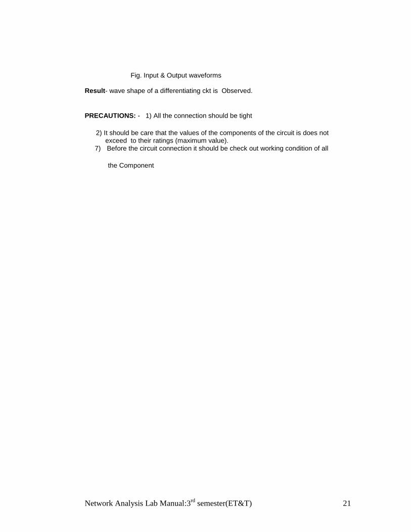
Network Analysis Lab Manual3rd
semester(ETampT) 28
Experiment 9
Objective- Measurement of capacitance of a condenser without using RLC bridge
Theory - A capacitor is a common electronic circuit component that consists of two parallel plates separated by an insulating material called a dielectric When a battery with
voltage is connected across the capacitor equal and opposite charges rapidly collect onto the plates due to the electric field created by the wires connecting the two plates
1
Once the plates are fully charged one plate will have a net positive charge while the
other plate will have a net negative charge It has been shown empirically that the
charge on one of the plates is directly proportional to the applied potential
difference and the constant of proportionality is known as the capacitance2 The
amount of charge on each plate in this steady-state is then written as
(1)
where is in coulombs is in volts and is in farads (after 19th century British
physicists Michael Faraday) That is A one-farad capacitor is physically
quite large so it is more common to see capacitors in the picofarad ( ) to
microfarad ( ) range Since the capacitor charges in some finite amount of time the charge that exists on one of the plates at any time that is before a steady-state exists is given by
(2)
When capacitors are connected together in series and then connected to a battery as shown in Figure 1 the same amount of charge must build up on each of the capacitors It can be shown that the behavior of these capacitors is as if there was one single capacitor
with an effective capacitance given by the following
Capacitors in series
(3)
It should be readily seen that the effective capacitance of capacitors in series is smaller than the capacitance of any of the contributing elements However when capacitors are connected inparallel as shown in Figure 2 the effective capacitance is given by the sum of each capacitance or
Capacitors in parallel
(4)
Network Analysis Lab Manual3rd
semester(ETampT) 29
Result - capacitance of a condenser is Measured without using RLC bridge
PRECAUTIONS - 1) All the connection should be tight
2) It should be care that the values of the components of the circuit is does not exceed to their ratings (maximum value)
8) Before the circuit connection it should be check out working condition of all the Component
Network Analysis Lab Manual3rd
semester(ETampT) 30
Experiment no 10
Objective - Function of
c Low pass filter
d High pass filter
e Band pass filter
Apparatus required - Op- Amp 741 Resistances capacitor Function generator Theory
A low-pass filter is a filter that passes low-frequency signals but attenuates (reduces
the amplitude of) signals with frequencies higher than the cutoff frequency The actual
amount of attenuation for each frequency varies from filter to filter It is sometimes called
a high-cut filter ortreble cut filter when used in audio applications A low-pass filter is the
opposite of a high-pass filter and a band-pass filter is a combination of a low-pass and a
high-pass
Low-pass filters exist in many different forms including electronic circuits (such as a hiss
filter used in audio) digital filters for smoothing sets of data acoustic barriers blurring of
images and so on The moving average operation used in fields such as finance is a
particular kind of low-pass filter and can be analyzed with the same signal
processing techniques as are used for other low-pass filters Low-pass filters provide a
smoother form of a signal removing the short-term fluctuations and leaving the longer-
term trend
Ideal and real filters
The sinc function the impulse responseof an ideal low-pass filter
An ideal low-pass filter completely eliminates all frequencies above the cutoff
frequency while passing those below unchanged its frequency response is a rectangular
Network Analysis Lab Manual3rd
semester(ETampT) 31
function and is a brick-wall filter The transition region present in practical filters does not
exist in an ideal filter An ideal low-pass filter can be realized mathematically
(theoretically) by multiplying a signal by the rectangular function in the frequency domain
or equivalently convolution with its impulse response a sinc function in the time
domain
However the ideal filter is impossible to realize without also having signals of infinite
extent in time and so generally needs to be approximated for real ongoing signals
because the sinc functions support region extends to all past and future times The filter
would therefore need to have infinite delay or knowledge of the infinite future and past in
order to perform the convolution It is effectively realizable for pre-recorded digital signals
by assuming extensions of zero into the past and future or more typically by making the
signal repetitive and using Fourier analysis
Real filters for real-time applications approximate the ideal filter by truncating
and windowing the infinite impulse response to make a finite impulse response applying
that filter requires delaying the signal for a moderate period of time allowing the
computation to see a little bit into the future This delay is manifested as phase shift
Greater accuracy in approximation requires a longer delay
An ideal low-pass filter results in ringing artifacts via the Gibbs phenomenon These can
be reduced or worsened by choice of windowing function and the design and choice of
real filters involves understanding and minimizing these artifacts For example simple
truncation [of sinc] causes severe ringing artifacts in signal reconstruction and to
reduce these artifacts one uses window functions which drop off more smoothly at the
edges[2]
The WhittakerndashShannon interpolation formula describes how to use a perfect low-pass
filter to reconstruct a continuous signal from a sampleddigital signal Real digital-to-
analog converters use real filter approximations
Function of filters
Network Analysis Lab Manual3rd
semester(ETampT) 32
There are many different types of filter circuits with different responses to changing
frequency The frequency response of a filter is generally represented using a Bode plot
and the filter is characterized by its cutoff frequency and rate of frequency rolloff In all
cases at the cutoff frequencythe filter attenuates the input power by half or 3 dB So
the order of the filter determines the amount of additional attenuation for frequencies
higher than the cutoff frequency
A first-order filter for example will reduce the signal amplitude by half (so power
reduces by a factor of 4) or 6 dB every time the frequency doubles (goes up
one octave) more precisely the power rolloff approaches 20 dB per decade in the
limit of high frequency The magnitude Bode plot for a first-order filter looks like a
horizontal line below the cutoff frequency and a diagonal line above the cutoff
frequency There is also a knee curve at the boundary between the two which
smoothly transitions between the two straight line regions If thetransfer function of a
first-order low-pass filter has a zero as well as apole the Bode plot will flatten out
again at some maximum attenuation of high frequencies such an effect is caused
for example by a little bit of the input leaking around the one-pole filter this one-polendash
one-zero filter is still a first-order low-pass See Polendashzero plot and RC circuit
A second-order filter attenuates higher frequencies more steeply The Bode plot
for this type of filter resembles that of a first-order filter except that it falls off more
quickly For example a second-order Butterworth filter will reduce the signal
amplitude to one fourth its original level every time the frequency doubles (so power
decreases by 12 dB per octave or 40 dB per decade) Other all-pole second-order
filters may roll off at different rates initially depending on their Q factor but approach
the same final rate of 12 dB per octave as with the first-order filters zeroes in the
transfer function can change the high-frequency asymptote See RLC circuit
Third- and higher-order filters are defined similarly In general the final rate of
power rolloff for an order-n all-pole filter is 6n dB per octave (ie 20n dB per
decade)
Network Analysis Lab Manual3rd
semester(ETampT) 33
Waveform
The gain-magnitude frequency response of a first-order (one-pole) low-pass filter Power
gain is shown in decibels (ie a 3 dB decline reflects an additional half-power
attenuation) Angular frequency is shown on a logarithmic scale in units of radians per
second
On any Butterworth filter if one extends the horizontal line to the right and the diagonal
line to the upper-left (the asymptotes of the function) they will intersect at exactly the
cutoff frequency The frequency response at the cutoff frequency in a first-order filter is
3 dB below the horizontal line The various types of filters ndash Butterworth filter Chebyshev
filter Bessel filter etc ndash all have different-looking knee curves Many second-order
filters are designed to have peaking or resonance causing their frequency response at
the cutoff frequency to be abovethe horizontal line See electronic filter for other types
High pass filter A high-pass filter or HPF is an LTI filter that passes high frequencies well but attenuates (ie reduces the amplitude of) frequencies lower than the filters cutoff frequency The actual amount of attenuation for each frequency is a design parameter of the filter It is sometimes called a low-cut filter or bass-cut filter
[1]
Network Analysis Lab Manual3rd
semester(ETampT) 34
function of high pass filter
The simple first-order electronic high-pass filter shown in Figure 1 is implemented by
placing an input voltage across the series combination of a capacitor and a resistor and
using the voltage across the resistor as an output The product of the resistance and
capacitance (RtimesC) is the time constant (τ) it is inversely proportional to the cutoff
frequency fc at which the output power is half the input power That is
where fc is in hertz τ is in seconds R is in ohms and C is in farads
Figure 2 An active high-pass filter
Figure 2 shows an active electronic implementation of a first-order high-pass filter
using anoperational amplifier In this case the filter has a passband gain of -
R2R1 and has a corner frequency of
Because this filter is active it may have non-unity passband gain That is
high-frequency signals are inverted and amplified by R2R1
band-pass filter
A band-pass filter is a device that passes frequencies within a certain range and rejects (attenuates) frequencies outside that range An example of an analogueelectronic band-pass filter is an RLC circuit (a resistorndashinductorndashcapacitor circuit) These filters can also be created by combining a low-pass filter with a high-pass filter
[1]
Network Analysis Lab Manual3rd
semester(ETampT) 35
Function of Band pass
Band pass is an adjective that describes a type of filter or filtering process it is frequently
confused with passband which refers to the actual portion of affected spectrum The two
words are both compound words that follow the English rules of formation the primary
meaning is the latter part of the compound while the modifier is the first part Hence one
may correctly say A dual bandpass filter has two passbands A bandpass signal is a
signal containing a band of frequencies away from zero frequency such as a signal that
comes out of a bandpass filter[2]
An ideal bandpass filter would have a completely flat passband (eg with no
gainattenuation throughout) and would completely attenuate all frequencies outside the
passband Additionally the transition out of the passband would be instantaneous in
frequency In practice no bandpass filter is ideal The filter does not attenuate all
frequencies outside the desired frequency range completely in particular there is a
region just outside the intended passband where frequencies are attenuated but not
rejected This is known as the filter roll-off and it is usually expressed in dB of attenuation
per octave or decade of frequency Generally the design of a filter seeks to make the
roll-off as narrow as possible thus allowing the filter to perform as close as possible to its
intended design Often this is achieved at the expense of pass-band or stop-band ripple
The bandwidth of the filter is simply the difference between the upper and lower cutoff
frequencies The shape factor is the ratio of bandwidths measured using two different
attenuation values to determine the cutoff frequency eg a shape factor of 21 at 303
dB means the bandwidth measured between frequencies at 30 dB attenuation is twice
that measured between frequencies at 3 dB attenuation
Waveform
Network Analysis Lab Manual3rd
semester(ETampT) 36
Bandwidth measured at half-power points (gain -3 dB radic22 or about 0707 relative to
peak) on a diagram showing magnitude transfer function versus frequency for a band-
pass filter
A medium-complexity example of a band-Pass filter Result -Function of Low pass filter High pass filter Band pass filter are studied
PRECAUTIONS - 1) All the connection should be tight
2) It should be care that the values of the components of the circuit is does not exceed to their ratings (maximum value)
9) Before the circuit connection it should be check out working condition of all the Component
Network Analysis Lab Manual3rd
semester(ETampT) 37
Experiment ndash 11 and 12 Objective - Find different electrical parameter in RLRCRLC series circuits and draw the
2 Phasor diagram and
a Determine current and PF in each case
b Determine and observe the resonance condition
Apparatus required Voltmeters Watt meter Rheostat Inductor Capacitor 1 KVA 1autotransformer Theory
An RLC circuit (or LCR circuit) is an electrical circuit consisting of a resistor an inductor and a capacitor connected in series or in parallel The RLC part of the name is due to those letters being the usual electrical symbols for resistance inductance and capacitance respectively The circuit forms a harmonic oscillator for current and will resonate in just the same way as an LC circuit will The difference that the presence of the resistor makes is that any oscillation induced in the circuit will die away over time if it not kept going by a source This effect of the resistor is called damping Some resistance is unavoidable in real circuits even if a resistor is not specifically included as a component A pure LC circuit is an ideal which really only exists in theory
A series RLC circuit a resistor inductor and a capacitor
Resonance
An important property of this circuit is its ability to resonate at a specific frequency the resonance frequency Frequencies are measured in units of hertz In this article however angular frequency is used which is more mathematically convenient This is measured in radians per second They are related to each other by a simple proportion
Natural frequency
The resonance frequency is defined in terms of the impedance presented to a driving source It is still possible for the circuit to carry on oscillating (for a time) after the driving source has been removed or it is subjected to a step in voltage (including a step down to
Network Analysis Lab Manual3rd
semester(ETampT) 38
zero) This is similar to the way that a tuning fork will carry on ringing after it has been struck and the effect is often called ringing This effect is the undriven natural resonance frequency of the circuit and in general is not exactly the same as the driven resonance frequency although the two will usually be quite close to each other Various terms are used by different authors to distinguish the two but resonance frequency unqualified usually means the driven resonance frequency The driven frequency may be called the undamped resonance frequency or undamped natural frequency and the undriven frequency may be called the damped resonance frequency or the damped natural frequency The reason for this terminology is that the driven resonance frequency in a series or parallel resonant circuit has the value
[1]
Damping
Damping is caused by the resistance in the circuit It determines whether or not the circuit will resonate naturally (that is without a driving source) Circuits which will resonate in this way are described as underdamped and those that will not are overdamped Damping attenuation (symbol α) is measured in nepers per second However the unitless damping factor (symbol ζ) is often a more useful measure which is related to α by
Bandwidth
The resonance effect can be used for filtering the rapid change in impedance near resonance can be used to pass or block signals close to the resonance frequency Both band-pass and band-stop filters can be constructed and some filter circuits are shown later in the article A key parameter in filter design is bandwidth The bandwidth is measured between the 3dB-points that is the frequencies at which the power passed through the circuit has fallen to half the value passed at resonance There are two of these half-power frequencies one above and one below the resonance frequency
Q factor
The Q factor is a widespread measure used to characterise resonators It is defined as the peak energy stored in the circuit divided by the average energy dissipated in it per cycle at resonance Low Q circuits are therefore damped and lossy and high Q circuits are underdamped Q is related to bandwidth low Q circuits are wide band and high Q circuits are narrow band In fact it happens that Q is the inverse of fractional bandwidth
Series RLC circuit
Network Analysis Lab Manual3rd
semester(ETampT) 39
RLC series circuit V - the voltage of the power source I - the current in the circuit R - the resistance of the resistor L - the inductance of the inductor C - the capacitance of the capacitor
In this circuit the three components are all in series with the voltage source The governing differential equation can be found by substituting into Kirchhoffs voltage law (KVL) the constitutive equation for each of the three elements From KVL
where are the voltages across R L and C respectively and is the time varying voltage from the source Substituting in the constitutive equations
For the case where the source is an unchanging voltage differentiating and dividing by L leads to the second order differential equation
This can usefully be expressed in a more generally applicable form
and are both in units of angular frequency is called the neper frequency or attenuation and is a measure of how fast the transient response of the circuit will die away after the stimulus has been removed Neper occurs in the name because the units can also be considered to be nepers per second neper being a unit of attenuation is the angular resonance frequency and is discussed later
[2]
Transient response
Plot showing underdamped and overdamped responses of a series RLC circuit The critical damping plot is the bold red curve The plots are normalised for L=1 C=1 and
The differential equation for the circuit solves in three different ways depending on the value of These are underdamped () overdamped () and critically damped () The differential equation has the characteristic equation
[6]
The roots of the equation in s are The general solution of the differential equation is an exponential in either root or a linear superposition of both
The coefficients A1 and A2 are determined by the boundary conditions of the specific problem being analysed That is they are set by the values of the currents and voltages in the circuit at the onset of the transient and the presumed value they will settle to after infinite time
A resistor-inductor circuit (RL circuit) or RL filter or RL network is one of the simplest analogue infinite impulse response electronic filters It consists of a resistor and an inductor either in series or in parallel driven by a voltage source
The fundamental passive linear circuit elements are the resistor (R) capacitor (C) and inductor (L) These circuit elements can be combined to form an electrical circuit in four distinct ways the RC circuit the RL circuit the LC circuit and the RLC circuit with the abbreviations indicating which components are used These circuits exhibit important
Network Analysis Lab Manual3rd
semester(ETampT) 40
types of behaviour that are fundamental to analogue electronics In particular they are able to act as passive filters This article considers the RL circuit in both series and parallel as shown in the diagrams
In practice however capacitors (and RC circuits) are usually preferred to inductors since they can be more easily manufactured and are generally physically smaller particularly for higher values of components
The Vectors in an LC Series Circuit
The vectors for this example circuit are shown to the right This time the composite phase angle is positive instead of negative because VL leads IL But to determine just what that phase angle is we must start by determining XL and then calculating the rest of the circuit parameters
XL=2 fL
I=EZ
VL= I XL
VR= I times R
Network Analysis Lab Manual3rd
semester(ETampT) 41
RC Circuits
A parallel RC Circuit
No RC does not stand for Remote Control An RC circuit is a circuit that has both a resistor (R) and a capacitor (C) Like the RL Circuit we will combine the resistor and the source on one side of the circuit and combine them into a thevening source Then if we apply KVL around the resulting loop we get the following equation
Circuit diagram
STEPWISE PROCEDURE ndash Discharge the capacitor before and after use ndash Connect the circuit as shown in figure
Network Analysis Lab Manual3rd
semester(ETampT) 42
ndash Initially set the autotransformer to zero position and rheostat to maximum position Switch ―ON the supply ndash Apply suitable voltage so that desired current flows in the circuit ndash Record the values of V I VR VL VC by varying resistance keeping inductance unchanged ndash Record the values of V I VR VL VC by varying inductance Keeping resistance unchanged ndash Reduce the voltage to zero and switch ―OFF the supply
ndash Draw the phasor diagram for each reading
Observation table
Resistance of inductor = r = helliphelliphellip
Table for measured and calculated values of V I etc
Power consumed by circuit = helliphellip Watt Phasor diagram
Network Analysis Lab Manual3rd
semester(ETampT) 43
Series Resonance
The resonance of a series RLC circuit occurs when the inductive and capacitive reactances are equal in magnitude but cancel each other because they are 180 degrees apart in phase The sharp minimum in impedance which occurs is useful in tuning applications The sharpness of the minimum depends on the value of R and is characterized by the Q of the circuit
Selectivity and Q of a Circuit
Resonant circuits are used to respond selectively to signals of a given frequency while discriminating against signals of different frequencies If the response of the circuit is more narrowly peaked around the chosen frequency we say that the circuit has higher selectivity A quality factor Q as described below is a measure of that selectivity and we speak of a circuit having a high Q if it is more narrowly selective
Network Analysis Lab Manual3rd
semester(ETampT) 44
An example of the application of resonant circuits is the selection of AM radio stations by the radio receiver The selectivity of the tuning must be high enough to discriminate strongly against stations above and below in carrier frequency but not so high as to discriminate against the sidebands created by the imposition of the signal by amplitude modulation
The selectivity of a circuit is dependent upon the amount of resistance in the circuit The variations on a series resonant circuit at right follow an example in Serway amp Beichner The smaller the resistance the higher the Q for given values of L and C The parallel resonant circuit is more commonly used in electronics but the algebra necessary to characterize the resonance is much more involved
Network Analysis Lab Manual3rd
semester(ETampT) 45
Using the same circuit parameters the illustration at left shows the power dissipated in the circuit as a function of frequency Since this power depends upon the square of the current these resonant curves appear steeper and narrower than the resonance peaks for current above
The quality factor Q is defined by
where Δω is the width of the resonant power curve at half maximum
Since that width turns out to be Δω =RL the value of Q can also be expressed as
The Q is a commonly used parameter in electronics with values usually in the range of Q=10 to 100 for circuit applications
Power in a Series Resonant Circuit
The average power dissipated in a series resonant circuit can be expressed in terms of the rms voltage and current as follows
Using the forms of the inductive reactance and capacitive reactance the term involving them can be expressed in terms of the frequency
where use has been made of the resonant frequency expression
Network Analysis Lab Manual3rd
semester(ETampT) 46
Substitution now gives the expression for average power as a function of frequency
This power distribution is plotted at left using the same circuit parameters as were used in the example on the Q factor of the series resonant circuit
The average power at resonance is just
since at the resonant frequency ω0 the reactive parts cancel so that the circuit appears as just the resistance R
Result -different electrical parameter in RLRCRLC series circuits are found
PRECAUTIONS - 1) All the connection should be tight
2) It should be care that the values of the components of the circuit is does not exceed to their ratings (maximum value)
10) Before the circuit connection it should be check out working condition of all the Component
Network Analysis Lab Manual3rd
semester(ETampT) 47
Experiment 13 and 14
Objective ndash Find different electrical parameter in R-C amp R-L-C parallel circuit and draw the 1)Phasor diagram 2) Find power and PF of the circuit 3)Observe parallel resonance condition
Apparatus required ndash RLC kit wires
Theory -
Parallel Resonance
The resonance of a parallel RLC circuit is a bit more involved than the series resonance The resonant frequency can be defined in three different ways which converge on the same expression as the series resonant frequency if the resistance of the circuit is small
In simple reactive circuits with little or no resistance the effects of radically altered impedance will manifest at the resonance frequency predicted by the equation given earlier In a parallel (tank) LC circuit this means infinite impedance at resonance In a series LC circuit it means zero impedance at resonance
However as soon as significant levels of resistance are introduced into most LC circuits this simple calculation for resonance becomes invalid Well take a look at several LC circuits with added resistance using the same values for capacitance and inductance as before 10 microF and 100 mH respectively According to our simple equation the resonant frequency should be 159155 Hz Watch though where current reaches maximum or minimum in the following SPICE
Network Analysis Lab Manual3rd
semester(ETampT) 48
Resonance Impedance Maximum
One of the ways to define resonance for a parallel RLC circuit is the frequency at which the impedance is maximum The general case is rather complex but the special case where the resistances of the inductor and capacitor are negligible can be handled readily by using the concept of admittance
Resonance Phase Definition
Defining the parallel resonant frequency as the frequency at which the voltage and current are in phase unity power factor gives the following expression for the resonant frequency
The above resonant frequency expression is obtained by taking the impedance expressions for the parallel RLC circuit and setting the expression for Xeq equal to zero to force the phase to zero After about a page of algebra the above expression emerges Note that for small values of the resistances this approaches the series resonant frequency
Admittance
Although the impedance Z is a far more common way to characterize the voltage-current relationships in an AC circuit there are times when the admittance is avaluable construct For a given circuit element the admittance is just the reciprocal of the impedance
The admittance has its most obvious utility in dealing with parallel AC circuits where there are no series elements The equivalent admittance of parallel elements is the sum of the admittances of the components
Response curve
Network Analysis Lab Manual3rd
semester(ETampT) 49
Inductor ringing due to resonance with stray capacitance
All inductors contain a certain amount of stray capacitance due to turn-to-turn and turn-to-core insulation gaps Also the placement of circuit conductors may create stray capacitance While clean circuit layout is important in eliminating much of this stray capacitance there will always be some that you cannot eliminate If this causes resonant problems (unwanted AC oscillations) added resistance may be a way to combat it If resistor R is large enough it will cause a condition of antiresonance dissipating enough energy to prohibit the inductance and stray capacitance from sustaining oscillations for very long
As was mentioned before the angle of this ―power triangle graphically indicates the ratio between the amount of dissipated (or consumed) power and the amount of absorbedreturned power It also happens to be the same angle as that of the circuits impedance in polar form When expressed as a fraction this ratio between true power and apparent power is called the power factor for this circuit Because true power and apparent power form the adjacent and hypotenuse sides of a right triangle respectively the power factor ratio is also equal to the cosine of that phase angle Using values from the last example circuit
Network Analysis Lab Manual3rd
semester(ETampT) 50
The power loss within the capacitor is that portion of the total power applied to the capacitor that is not stored by the capacitor on an instantaneous basis As the current passes through the series resistance element it generates heat which is the power loss It should be noted that all energy losses (due to leads dielectric polarization connections and eddy currents in the electrode material) are taken into account by the equivalent series resistance element (see Technical Bulletin 10) Analysis of the power equation shows
Result ndash objective is reached
PRECAUTIONS - 1) All the connection should be tight
2) It should be care that the values of the components of the circuit is does not exceed to their ratings (maximum value)
11) Before the circuit connection it should be check out working condition of all
the Component
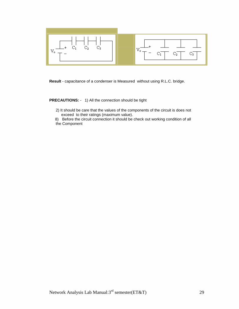
Network Analysis Lab Manual3rd
semester(ETampT) 36
Bandwidth measured at half-power points (gain -3 dB radic22 or about 0707 relative to
peak) on a diagram showing magnitude transfer function versus frequency for a band-
pass filter
A medium-complexity example of a band-Pass filter Result -Function of Low pass filter High pass filter Band pass filter are studied
PRECAUTIONS - 1) All the connection should be tight
2) It should be care that the values of the components of the circuit is does not exceed to their ratings (maximum value)
9) Before the circuit connection it should be check out working condition of all the Component
Network Analysis Lab Manual3rd
semester(ETampT) 37
Experiment ndash 11 and 12 Objective - Find different electrical parameter in RLRCRLC series circuits and draw the
2 Phasor diagram and
a Determine current and PF in each case
b Determine and observe the resonance condition
Apparatus required Voltmeters Watt meter Rheostat Inductor Capacitor 1 KVA 1autotransformer Theory
An RLC circuit (or LCR circuit) is an electrical circuit consisting of a resistor an inductor and a capacitor connected in series or in parallel The RLC part of the name is due to those letters being the usual electrical symbols for resistance inductance and capacitance respectively The circuit forms a harmonic oscillator for current and will resonate in just the same way as an LC circuit will The difference that the presence of the resistor makes is that any oscillation induced in the circuit will die away over time if it not kept going by a source This effect of the resistor is called damping Some resistance is unavoidable in real circuits even if a resistor is not specifically included as a component A pure LC circuit is an ideal which really only exists in theory
A series RLC circuit a resistor inductor and a capacitor
Resonance
An important property of this circuit is its ability to resonate at a specific frequency the resonance frequency Frequencies are measured in units of hertz In this article however angular frequency is used which is more mathematically convenient This is measured in radians per second They are related to each other by a simple proportion
Natural frequency
The resonance frequency is defined in terms of the impedance presented to a driving source It is still possible for the circuit to carry on oscillating (for a time) after the driving source has been removed or it is subjected to a step in voltage (including a step down to
Network Analysis Lab Manual3rd
semester(ETampT) 38
zero) This is similar to the way that a tuning fork will carry on ringing after it has been struck and the effect is often called ringing This effect is the undriven natural resonance frequency of the circuit and in general is not exactly the same as the driven resonance frequency although the two will usually be quite close to each other Various terms are used by different authors to distinguish the two but resonance frequency unqualified usually means the driven resonance frequency The driven frequency may be called the undamped resonance frequency or undamped natural frequency and the undriven frequency may be called the damped resonance frequency or the damped natural frequency The reason for this terminology is that the driven resonance frequency in a series or parallel resonant circuit has the value
[1]
Damping
Damping is caused by the resistance in the circuit It determines whether or not the circuit will resonate naturally (that is without a driving source) Circuits which will resonate in this way are described as underdamped and those that will not are overdamped Damping attenuation (symbol α) is measured in nepers per second However the unitless damping factor (symbol ζ) is often a more useful measure which is related to α by
Bandwidth
The resonance effect can be used for filtering the rapid change in impedance near resonance can be used to pass or block signals close to the resonance frequency Both band-pass and band-stop filters can be constructed and some filter circuits are shown later in the article A key parameter in filter design is bandwidth The bandwidth is measured between the 3dB-points that is the frequencies at which the power passed through the circuit has fallen to half the value passed at resonance There are two of these half-power frequencies one above and one below the resonance frequency
Q factor
The Q factor is a widespread measure used to characterise resonators It is defined as the peak energy stored in the circuit divided by the average energy dissipated in it per cycle at resonance Low Q circuits are therefore damped and lossy and high Q circuits are underdamped Q is related to bandwidth low Q circuits are wide band and high Q circuits are narrow band In fact it happens that Q is the inverse of fractional bandwidth
Series RLC circuit
Network Analysis Lab Manual3rd
semester(ETampT) 39
RLC series circuit V - the voltage of the power source I - the current in the circuit R - the resistance of the resistor L - the inductance of the inductor C - the capacitance of the capacitor
In this circuit the three components are all in series with the voltage source The governing differential equation can be found by substituting into Kirchhoffs voltage law (KVL) the constitutive equation for each of the three elements From KVL
where are the voltages across R L and C respectively and is the time varying voltage from the source Substituting in the constitutive equations
For the case where the source is an unchanging voltage differentiating and dividing by L leads to the second order differential equation
This can usefully be expressed in a more generally applicable form
and are both in units of angular frequency is called the neper frequency or attenuation and is a measure of how fast the transient response of the circuit will die away after the stimulus has been removed Neper occurs in the name because the units can also be considered to be nepers per second neper being a unit of attenuation is the angular resonance frequency and is discussed later
[2]
Transient response
Plot showing underdamped and overdamped responses of a series RLC circuit The critical damping plot is the bold red curve The plots are normalised for L=1 C=1 and
The differential equation for the circuit solves in three different ways depending on the value of These are underdamped () overdamped () and critically damped () The differential equation has the characteristic equation
[6]
The roots of the equation in s are The general solution of the differential equation is an exponential in either root or a linear superposition of both
The coefficients A1 and A2 are determined by the boundary conditions of the specific problem being analysed That is they are set by the values of the currents and voltages in the circuit at the onset of the transient and the presumed value they will settle to after infinite time
A resistor-inductor circuit (RL circuit) or RL filter or RL network is one of the simplest analogue infinite impulse response electronic filters It consists of a resistor and an inductor either in series or in parallel driven by a voltage source
The fundamental passive linear circuit elements are the resistor (R) capacitor (C) and inductor (L) These circuit elements can be combined to form an electrical circuit in four distinct ways the RC circuit the RL circuit the LC circuit and the RLC circuit with the abbreviations indicating which components are used These circuits exhibit important
Network Analysis Lab Manual3rd
semester(ETampT) 40
types of behaviour that are fundamental to analogue electronics In particular they are able to act as passive filters This article considers the RL circuit in both series and parallel as shown in the diagrams
In practice however capacitors (and RC circuits) are usually preferred to inductors since they can be more easily manufactured and are generally physically smaller particularly for higher values of components
The Vectors in an LC Series Circuit
The vectors for this example circuit are shown to the right This time the composite phase angle is positive instead of negative because VL leads IL But to determine just what that phase angle is we must start by determining XL and then calculating the rest of the circuit parameters
XL=2 fL
I=EZ
VL= I XL
VR= I times R
Network Analysis Lab Manual3rd
semester(ETampT) 41
RC Circuits
A parallel RC Circuit
No RC does not stand for Remote Control An RC circuit is a circuit that has both a resistor (R) and a capacitor (C) Like the RL Circuit we will combine the resistor and the source on one side of the circuit and combine them into a thevening source Then if we apply KVL around the resulting loop we get the following equation
Circuit diagram
STEPWISE PROCEDURE ndash Discharge the capacitor before and after use ndash Connect the circuit as shown in figure
Network Analysis Lab Manual3rd
semester(ETampT) 42
ndash Initially set the autotransformer to zero position and rheostat to maximum position Switch ―ON the supply ndash Apply suitable voltage so that desired current flows in the circuit ndash Record the values of V I VR VL VC by varying resistance keeping inductance unchanged ndash Record the values of V I VR VL VC by varying inductance Keeping resistance unchanged ndash Reduce the voltage to zero and switch ―OFF the supply
ndash Draw the phasor diagram for each reading
Observation table
Resistance of inductor = r = helliphelliphellip
Table for measured and calculated values of V I etc
Power consumed by circuit = helliphellip Watt Phasor diagram
Network Analysis Lab Manual3rd
semester(ETampT) 43
Series Resonance
The resonance of a series RLC circuit occurs when the inductive and capacitive reactances are equal in magnitude but cancel each other because they are 180 degrees apart in phase The sharp minimum in impedance which occurs is useful in tuning applications The sharpness of the minimum depends on the value of R and is characterized by the Q of the circuit
Selectivity and Q of a Circuit
Resonant circuits are used to respond selectively to signals of a given frequency while discriminating against signals of different frequencies If the response of the circuit is more narrowly peaked around the chosen frequency we say that the circuit has higher selectivity A quality factor Q as described below is a measure of that selectivity and we speak of a circuit having a high Q if it is more narrowly selective
Network Analysis Lab Manual3rd
semester(ETampT) 44
An example of the application of resonant circuits is the selection of AM radio stations by the radio receiver The selectivity of the tuning must be high enough to discriminate strongly against stations above and below in carrier frequency but not so high as to discriminate against the sidebands created by the imposition of the signal by amplitude modulation
The selectivity of a circuit is dependent upon the amount of resistance in the circuit The variations on a series resonant circuit at right follow an example in Serway amp Beichner The smaller the resistance the higher the Q for given values of L and C The parallel resonant circuit is more commonly used in electronics but the algebra necessary to characterize the resonance is much more involved
Network Analysis Lab Manual3rd
semester(ETampT) 45
Using the same circuit parameters the illustration at left shows the power dissipated in the circuit as a function of frequency Since this power depends upon the square of the current these resonant curves appear steeper and narrower than the resonance peaks for current above
The quality factor Q is defined by
where Δω is the width of the resonant power curve at half maximum
Since that width turns out to be Δω =RL the value of Q can also be expressed as
The Q is a commonly used parameter in electronics with values usually in the range of Q=10 to 100 for circuit applications
Power in a Series Resonant Circuit
The average power dissipated in a series resonant circuit can be expressed in terms of the rms voltage and current as follows
Using the forms of the inductive reactance and capacitive reactance the term involving them can be expressed in terms of the frequency
where use has been made of the resonant frequency expression
Network Analysis Lab Manual3rd
semester(ETampT) 46
Substitution now gives the expression for average power as a function of frequency
This power distribution is plotted at left using the same circuit parameters as were used in the example on the Q factor of the series resonant circuit
The average power at resonance is just
since at the resonant frequency ω0 the reactive parts cancel so that the circuit appears as just the resistance R
Result -different electrical parameter in RLRCRLC series circuits are found
PRECAUTIONS - 1) All the connection should be tight
2) It should be care that the values of the components of the circuit is does not exceed to their ratings (maximum value)
10) Before the circuit connection it should be check out working condition of all the Component
Network Analysis Lab Manual3rd
semester(ETampT) 47
Experiment 13 and 14
Objective ndash Find different electrical parameter in R-C amp R-L-C parallel circuit and draw the 1)Phasor diagram 2) Find power and PF of the circuit 3)Observe parallel resonance condition
Apparatus required ndash RLC kit wires
Theory -
Parallel Resonance
The resonance of a parallel RLC circuit is a bit more involved than the series resonance The resonant frequency can be defined in three different ways which converge on the same expression as the series resonant frequency if the resistance of the circuit is small
In simple reactive circuits with little or no resistance the effects of radically altered impedance will manifest at the resonance frequency predicted by the equation given earlier In a parallel (tank) LC circuit this means infinite impedance at resonance In a series LC circuit it means zero impedance at resonance
However as soon as significant levels of resistance are introduced into most LC circuits this simple calculation for resonance becomes invalid Well take a look at several LC circuits with added resistance using the same values for capacitance and inductance as before 10 microF and 100 mH respectively According to our simple equation the resonant frequency should be 159155 Hz Watch though where current reaches maximum or minimum in the following SPICE
Network Analysis Lab Manual3rd
semester(ETampT) 48
Resonance Impedance Maximum
One of the ways to define resonance for a parallel RLC circuit is the frequency at which the impedance is maximum The general case is rather complex but the special case where the resistances of the inductor and capacitor are negligible can be handled readily by using the concept of admittance
Resonance Phase Definition
Defining the parallel resonant frequency as the frequency at which the voltage and current are in phase unity power factor gives the following expression for the resonant frequency
The above resonant frequency expression is obtained by taking the impedance expressions for the parallel RLC circuit and setting the expression for Xeq equal to zero to force the phase to zero After about a page of algebra the above expression emerges Note that for small values of the resistances this approaches the series resonant frequency
Admittance
Although the impedance Z is a far more common way to characterize the voltage-current relationships in an AC circuit there are times when the admittance is avaluable construct For a given circuit element the admittance is just the reciprocal of the impedance
The admittance has its most obvious utility in dealing with parallel AC circuits where there are no series elements The equivalent admittance of parallel elements is the sum of the admittances of the components
Response curve
Network Analysis Lab Manual3rd
semester(ETampT) 49
Inductor ringing due to resonance with stray capacitance
All inductors contain a certain amount of stray capacitance due to turn-to-turn and turn-to-core insulation gaps Also the placement of circuit conductors may create stray capacitance While clean circuit layout is important in eliminating much of this stray capacitance there will always be some that you cannot eliminate If this causes resonant problems (unwanted AC oscillations) added resistance may be a way to combat it If resistor R is large enough it will cause a condition of antiresonance dissipating enough energy to prohibit the inductance and stray capacitance from sustaining oscillations for very long
As was mentioned before the angle of this ―power triangle graphically indicates the ratio between the amount of dissipated (or consumed) power and the amount of absorbedreturned power It also happens to be the same angle as that of the circuits impedance in polar form When expressed as a fraction this ratio between true power and apparent power is called the power factor for this circuit Because true power and apparent power form the adjacent and hypotenuse sides of a right triangle respectively the power factor ratio is also equal to the cosine of that phase angle Using values from the last example circuit
Network Analysis Lab Manual3rd
semester(ETampT) 50
The power loss within the capacitor is that portion of the total power applied to the capacitor that is not stored by the capacitor on an instantaneous basis As the current passes through the series resistance element it generates heat which is the power loss It should be noted that all energy losses (due to leads dielectric polarization connections and eddy currents in the electrode material) are taken into account by the equivalent series resistance element (see Technical Bulletin 10) Analysis of the power equation shows
Result ndash objective is reached
PRECAUTIONS - 1) All the connection should be tight
2) It should be care that the values of the components of the circuit is does not exceed to their ratings (maximum value)
11) Before the circuit connection it should be check out working condition of all
the Component
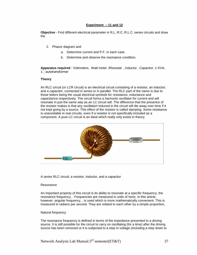
Network Analysis Lab Manual3rd
semester(ETampT) 50
The power loss within the capacitor is that portion of the total power applied to the capacitor that is not stored by the capacitor on an instantaneous basis As the current passes through the series resistance element it generates heat which is the power loss It should be noted that all energy losses (due to leads dielectric polarization connections and eddy currents in the electrode material) are taken into account by the equivalent series resistance element (see Technical Bulletin 10) Analysis of the power equation shows
Result ndash objective is reached
PRECAUTIONS - 1) All the connection should be tight
2) It should be care that the values of the components of the circuit is does not exceed to their ratings (maximum value)
11) Before the circuit connection it should be check out working condition of all
the Component