GOODRAM Industrial Compact Flash Card (SLC) … -VS1 O 33 -VS1 O 33 -VS1 I 34 -IORD I 34 -IORD I 34...
42
WILK ELEKTRONIK S.A. ul. Mikołowska 42, 43-173 Łaziska Górne, Poland Website: www.goodram.com | www.wilk.com.pl Tel: +48 (32) 736 90 00 Fax: +48 (32) 736 90 01 Wilk Elektronik S.A. GOODRAM Industrial Compact Flash Card (SLC) Version 1.0 All rights are strictly reserved. Any portion of this paper shall not be reproduced, copied, or translated to any other forms without permission from Wilk Elektronik S.A.
Transcript of GOODRAM Industrial Compact Flash Card (SLC) … -VS1 O 33 -VS1 O 33 -VS1 I 34 -IORD I 34 -IORD I 34...

WILK ELEKTRONIK S.A.
ul. Mikołowska 42, 43-173 Łaziska Górne, Poland
Website: www.goodram.com | www.wilk.com.pl
Tel: +48 (32) 736 90 00
Fax: +48 (32) 736 90 01
Wilk Elektronik S.A.
GOODRAM Industrial Compact Flash Card (SLC)
Version 1.0
All rights are strictly reserved. Any portion of this paper shall not be reproduced, copied, or
translated to any other forms without permission from Wilk Elektronik S.A.

This document is subjected to change without any notice.
Please contact your Wilk Elektronik S.A. sales representative for details as to environmental matters such as
the RoHS compatibility of Product. Please use Product in compliance with all applicable laws and regulations
that regulate the inclusion or use of controlled substances, including without limitation, the EU RoHS
Directive. Wilk Elektronik S.A. assumes no liability for damages or losses occurring as a result of
noncompliance with applicable laws and regulations.

Contents
1. General Description ................................................................................................................................... 4
1.1. Overview ...................................................................................................................................... 4
1.2. System Features ........................................................................................................................... 4
2. Product Specifications ............................................................................................................................... 5
3. Pin Assignment and Description ................................................................................................................ 6
4. Identify Drive Information ....................................................................................................................... 14
5. CIS Information ........................................................................................................................................ 16
6. Power Management ................................................................................................................................ 21
7. System Power Consumption ................................................................................................................... 23
8. Electrical Specifications ........................................................................................................................... 23
9. DC Characteristics .................................................................................................................................... 24
10. AC Characteristics ............................................................................................................................... 25
10.1. PCMCIA Interface ....................................................................................................................... 25
10.2. IDE Interface Timing (PIO Mode) ............................................................................................... 32
10.3. Multi Word DMA ....................................................................................................................... 34
10.4. Ultra DMA .................................................................................................................................. 36
11. Package Specifications ........................................................................................................................ 41
12. LBA and CHS Parameters .................................................................................................................... 41

1. General Description
1.1. Overview
CompactFlash™ Card is one of the most popular flash storage elements in the memory card
market. By offering excellent performance and wide compatibility, it also provides a wide range of
capacities available for users. In addition, industrial-grade CompactFlash™ cards are available for
any applications under rigorous environmental conditions, including extensive temperature, shock
and vibration.
1.2. System Features
Light weight and noiseless
Implemented with automatic error detection and retry capability
Support power-down commands and idle modes
Compatible with PC card and socket services
Host interface: 8/16 bit access
Auto-detection of CF/ATA host interface

2. Product Specifications Support Capacity:
- SLC: 1-32GB (Diamond & Silver)
- MLC: 2-64GB (Diamond & Silver)
Support the following host interfaces:
- PCMCIA/IDE Interface (Support up to PIO Mode 6/Multi Word DMA Mode4/PCMCIA
Ultra DMA Mode 5/Ultra DMA Mode 7)
- Fully compatible with CompactFlash Specification Version 3.x, 4.x, 5.x and 6.x
- Fully compatible with PC Card Standard Release 8.0
- Fully compatible with the IDE standard interface
Host Transfer Rate:
- For PC Card/CompactFlash: 25MB/s (PIO6)
- For IDE standard interface: 166MB/s (UDMA7)
Built-In NAND Flash Memory Interface
- Built-in hardware ECC circuit
- Support SLC and MLC NAND flash memory
- Support 4KB /8KB data per page NAND flash memory
1T RISC uP8051 RAM Mode
- Internal RAM: 256 Bytes.
- External RAM: 24KB (On Chip)
Support SRAM Buffer (Dual Buffer Mode):
- A Buffer (512 Words)
- B Buffer (512 Words)
- CIS Buffer (256 bytes)
Operating Voltage: 3.0 ~ 5.5V
Support power-saving implementation
Environmental Conditions
- Operation Temp. Range:
o Silver Series: 0°C to 70°C (SLC & MLC)
o Diamond Series: ‐40°C to 85°C (SLC & MLC)
- Storage Temp. Range: ‐40°C to 85°C
- Humidity: RH 95% under 55°C (In operation)
- Shock*: 1500G/0.5ms
- Vibration*: 80‐2000Hz/20G
- Acoustic = 0dB
*Subject to be changed without notice.

3. Pin Assignment and Description
Pin Assignments of Compact Flash Interface
PC Card Memory Mode PC Card I/O Mode True IDE Mode
Pin # Signal Name Pin Type Pin # Signal Name Pin Type Pin # Signal Name Pin Type
1 GND 1 GND 1 GND I/O
2 D03 I/O 2 D03 I/O 2 D03 I/O
3 D04 I/O 3 D04 I/O 3 D04 I/O
4 D05 I/O 4 D05 I/O 4 D05 I/O
5 D06 I/O 5 D06 I/O 5 D06 I/O
6 D07 I/O 6 D07 I/O 6 D07 I
7 -CE1 I 7 -CE1 I 7 -CSO I
8 A10 I 8 A10 I 8 A10 I
9 -OE I 9 -OE I 9 -ATA SEL I
10 A09 I 10 A09 I 10 A09 I
11 A08 I 11 A08 I 11 A08 I
12 A07 I 12 A07 I 12 A07
13 VCC 13 VCC 13 VCC I
14 A06 I 14 A06 I 14 A06 I
15 A05 I 15 A05 I 15 A05 I
16 A04 I 16 A04 I 16 A04 I
17 A03 I 17 A03 I 17 A03 I
18 A02 I 18 A02 I 18 A02 I
19 A01 I 19 A01 I 19 A01 I
20 A00 I 20 A00 I 20 A00 I/O
21 D00 I/O 21 D00 I/O 21 D00 I/O
22 D01 I/O 22 D01 I/O 22 D01 I/O
23 D02 I/O 23 D02 I/O 23 D02 O
24 WP O 24 -IOIS16 O 24 -IOIS16 O
25 -CD2 O 25 -CD2 O 25 -CD2 O
26 -CD1 O 26 -CD1 O 26 -CD1 I/O
27 D11 I/O 27 D11 I/O 27 D11 I/O
28 D12 I/O 28 D12 I/O 28 D12 I/O
29 D13 I/O 29 D13 I/O 29 D13 I/O
30 D14 I/O 30 D14 I/O 30 D14 I/O
31 D15 I/O 31 D15 I/O 31 D15 I
32 -CE2 I 32 -CE2 I 32 -CS1 O

33 -VS1 O 33 -VS1 O 33 -VS1 I
34 -IORD I 34 -IORD I 34 -IORD I
35 -IOWR I 35 -IOWR I 35 -IOWR I
36 -WE I 36 -WE I 36 -WE I
37 RDY/BSY O 37 IREQ O 37 INTRQ
38 VCC 38 VCC 38 VCC I
39 -CSEL I 39 -CSEL I 39 -CSEL I
40 -VS2 O 40 -VS2 O 40 -VS2 I
41 RESET I 41 RESET I 41 RESET O
42 -WAIT O 42 -WAIT O 42 IORDY O
43 -INPACK O 43 -INPACK O 43 -INPACK I
44 -REG I 44 -REG I 44 -REG I/O
45 BVD2 I/O 45 -SPKR I/O 45 -DASP I/O
46 BVD1 I/O 46 -STSCHG I/O 46 -PDIAG I/O
47 D08 I/O 47 D08 I/O 47 D08 I/O
48 D09 I/O 48 D09 I/O 48 D09 I/O
49 D10 I/O 49 D10 I/O 49 D10
50 GND 50 GND 50 GND
NOTES:
1. WE in True IDE mode should be connected to VCC.
2. CSEL in True IDE mode is the input pin for master/slave selection used.

Signal Descriptions
Signal Name Dir. Pin Description
BVD2 (PC Card Memory Mode)
I/O 45
This output line is always driven to a high state in Memory Mode since a battery is not required for this product.
-SPKR (PC CARD I/O Mode)
This output line is always driven to a high state in I/O Mode since this product does not support the audio function.
-DASP (True IDE Mode)
In the True IDE Mode, this input/output is the Disk Active/Slave Present signal in the Master/Slave handshake protocol.
-CD1,-CD2 (PC Card Memory Mode)
O 26, 25
These card detect pins are connected to the ground on the CompactFlashTM Storage Card. They are used by the host to determine if the CompactFlashTM Storage Card is fully inserted into its socket.
-CD1,-CD2 (PC Card I/O Mode)
The signal is the same for all modes.
-CD1,-CD2 (True IDE Mode)
The signal is the same for all modes.
D[15:0] (PC Card Memory Mode)
I/O
31, 30, 29, 28, 27, 49, 48, 47, 6, 5, 4,
3, 2, 23, 22, 21
These lines carry the Data, Commands, and Status information between the host and the controller. D00 is the LSB of the Odd Byte of the World.
D[15:0] (PC Card I/O Mode)
The signal is the same as the PC Card Memory Mode signal.
D[15:0] (True IDE Mode)
In True IDE Mode, all Task File operations occur in byte mode on the lower order bus D00-D07, while all data transfers are 16 bit using D00-D15.
-IOWR (PC Card Memory Mode)
I 35
This signal is not used in this mode.
-IOWR (PC Card I/O Mode)
The I/O Write strobe pulse is used to clock I/O data on the Card Data bus into the CompactFlashTM Storage Card or CF+ Card controller registers when the CompactFlashTM Storage Card or CF+ Card is configured to use the I/O interface. The clocking shall occur on the negative to positive edge of the signal (trailing edge).
-IOWR (True IDE Mode – Except Ultra DMA Protocol Active)
In True IDE Mode, while Ultra DMA mode protocol is not active, this signal has the same function as in PC Card I/O Mode. When Ultra DMA mode protocol is supported, this signal must be negated before entering Ultra DMA mode protocol.
STOP (True IDE Mode – Ultra DMA Protocol Active)
In True IDE Mode, while Ultra DMA mode protocol is active, the assertion of this signal causes the termination of the Ultra DMA burst.
-IORD (PC Card Memory Mode)
I 34 This signal is not used in this mode.

-IORD (PC Card I/O Mode)
This is an I/O Read strobe generated by the host. This signal gates I/O data onto the bus from the CompactFlashTM Storage Card or CF+ Card when the card is configured to use the I/O interface.
-IORD (True IDE Mode – Except Ultra DMA Protocol Active)
In True IDE Mode, while Ultra DMA mode is not active, this signal has the same function as in PC Card I/O Mode.
-HDMARDY (True IDE Mode – In Ultra DMA Protocol DMA Read)
In True IDE Mode when Ultra DMA mode DMA Read is active, this signal is asserted by the host to indicate that the host is ready to receive Ultra DMA data-in burst. The host may negate –HDMARDY to pause an Ultra DMA transfer.
-HSTROBE (True IDE Mode – In Ultra DMA Protocol DMA Write)
In True IDE Mode when Ultra DMA mode DMA Write is active, this signal is the data out strobe generated by the host. Both the rising and falling edge of HSTROBE cause data to be latched by the device. The host may stop generating HSTROBE edges to pause an Ultra DMA data-out burst.
-WE (PC Card Memory Mode)
I 36
This signal is driven by the host and used for strobing memory write data to the registers of the CompactFlashTM Storage Card when the card is configured in the memory interface mode. It is also used for writing the configuration registers.
-WE (PC Card I/O Mode)
In PC Card I/O Mode, this signal is used for writing the configuration registers.
-WE (True IDE Mode)
In True IDE Mode this input signal is not used and should be connected to VCC by the host.
-OE (PC Card Memory Mode)
I 9
This is an Ouput Enable strobe generated by the host interface. It is used to read data from the CompactFlashTM Storage Card in Memory Mode and to read the CIS and configuration registers.
-OE (PC Card I/O Mode)
In PC Card I/O Mode, this signal is used to read the CIS and configuration registers.
-OE (True IDE Mode)
To enable True IDE Mode, this input should be grounded by the host.
RDY/-BSY (PC Card Memory Mode)
O 37
In Memory Mode, this signal is set high when the CompactFlashTM Storage Card is ready to accept a new data transfer operation and is held low when the card is busy. The Host memory card socket must provide a pull-up resistor. At power up and at Reset, the RDY/-BSY is held low (busy) until the CompactFlashTM Storage Card has completed its power up or reset function. No access of any type should be made to the CompactFlashTM Storage Card during this time. The RDY/-BSY signal is held high (disabled from being busy) when the following condition is true: The CompactFlashTM Storage Card has been powered up with +RESET continuously disconnected or asserted.

-IREQ (PC Card I/O Mode)
I/O Operation- After the CompactFlashTM Storage has been configured for I/O operation, this signal is used as –Interrupt Request. This line is strobed low to generate a pulse mode interrupt or held low for a level mode interrupt.
INTRQ (True IDE Mode)
In True IDE Mode, this signal is an active high Interrupt Request to the host.
A[10:0] (PC Card Memory Mode)
I
8, 10, 11, 12, 14, 15, 16, 17, 18, 19,
20
These address lines along with the –REG signal are used to select the following: The I/O port address registers within the CompactFlashTM Storage Card, the memory mapped port address registers within the CompactFlashTM Storage Card, a byte in the card’s information structure and its configuration control and status registers.
A[10:0] (PC Card I/O Mode)
The signal is the same as the PC Card Memory Mode signal.
A[2:0] (True IDE Mode)
In True IDE Mode only HA [2:0] are used to select one of the eight registers in the Task File, the remaining address lines should be grounded by the host.
-CE1,-CE2 (PC Card Memory Mode) Card Enable
I 7, 32
These input signals are used to select the card and to indicate to the card whether a byte or a word operation is being performed. –CE2 always accesses the odd byte of the word. –CE1 accesses the even byte or the Odd byte of the word depending on the A0 and –CE2. A multiplexing scheme based on A0, -CE1, -CE2 allows 8 bit hosts to access all data on D0-D7.
-CE1,-CE2 (PC Card I/O Mode) Card Enable
This signal is the same as the PC Card Memory Mode signal.
-CS0,-CS1 (True IDE Mode)
In the True IDE Mode, CS0 is the chip select for the task file registers while CS1 is used to select the Alternate Status Register and the Device Control Register.
-CSEL (PC Card Memory Mode)
I 39
This signal is not used for this mode.
-CSEL (PC Card I/O Mode)
This signal is not used for this mode.
-CSEL (True IDE Mode)
This internal pull-up signal is used to configure this device as a Master or a Slave when configured in the True IDE Mode. When this pin is grounded, this device is configured as a Master. When the pin is open, this device is configured as a Slave.
-REG (PC Card Memory Mode) Attribute Memory Select I 44
This signal is used during Memory Cycles to distinguish between Common Memory and Register (Attribute) Memory accesses. High for Common Memory, Low for Attribute Memory
-REG (PC Card I/O Mode)
The signal shall also be active (low) during I/O Cycles when the I/O address is on the Bus.

-DMACK (True IDE Mode)
This is a DMA Acknowledge signal that is asserted by the host in response to DMARQ to initiate DMA transfers. While DMA operations are not active, the card shall ignore -DMACK signal, including a floating condition. If DMA operation is not supported by a True IDE Mode only host, this signal should be driven high or connected to VCC by the host. A host that does not support DMA mode and implements both PCMCIA and True-IDE modes of operation need not alter the PCMCIA mode connections while in True-IDE mode as long as this does not prevent proper operation all modes.
WP (PC Card Memory Mode) Write Protect
O 24
Memory Mode- The CompactFlashTM Storage Card does not have a write protect switch. This signal is held low after the addressed port.
-IOIS 16 (PC Card I/O Mode)
I/O Operation- When the CompactFlashTM Storage Card is configured for I/O Operation Pin 24 is used for the –I/O Selected is a 16 Bit Port (-IOIS16) function. A Low signal indicates that a 16 bit or odd byte only operation can be performed at the addressed port.
-IOIS 16 (True IDE Mode)
In True IDE Mode this output signal is asserted low when this device is expecting a word data transfer cycle.
-VS1 -VS2 (PC Card Memory Mode)
O 33 40
Voltage Sense Signals. –VS1 is grounded so that the CompactFlashTM Storage Card CIS can be read at 3.3 volts and –VS2 is reserved by PCMCIA for a secondary voltage.
-VS1 -VS2 (PC Card I/O Mode)
This signal is the same for all modes.
-VS1 -VS2 (True IDE Mode)
This signal is the same for all modes.
-INPACK (PC Card Memory Mode)
O 43
This signal is not used in this mode.
-INPACK (PC Card I/O Mode) Input Acknowledge
The Input Acknowledge signal is asserted by the CompactFlashTM Storage Card or CF+ Card when the card is selected and responding to an I/O read cycle at the address that is on the address bus. This signal is used by the host to control the enable of any input data buffers between CompactFlashTM Storage Card or CF+ Card and the CPU.

-DMARQ (True IDE Mode)
This signal is a DMA Request that is used for DMA data transfer between host and device. It shall be asserted by the device when it is ready to transfer data to or from the host. For Multiword DMA transfers, the direction of data transfer is controlled by –IORD and –IOWR. This signal is used in a handshake manner with –DMACK, ie., the device shall wait until the host asserts –DMACK before negating DMARQ, and re-asserting DMARQ if there is more data to transfer. DMARQ shall not be driven when the device is not selected. While a DMA operation is in progress, -CS0 and –CS1 shall be held negated and the width of the transfer shall be 16 bits. If there is no hardware support for DMA mode in the host, this output signal is not used and should not be connected at the host. In this case, the BIOS must report that DMA mode is not supported by the host so that device drivers will not attempt DMA mode. A host that does not support DMA mode and implements both PCMCIA and True-IDE modes of operation need not alter the PCMCIA mode connections while in True-IDE mode as long as this does not prevent proper operation in any mode.
BVD1 (PC Card Memory Mode)
I/O 46
This signal is asserted high as the BVD1 signal since a battery is not used with this product.
-STSCHG (PC Card I/O Mode) Status Changed
This signal is asserted low to alert the host to changes in the RDY/-BSY and Write Protect states, while the I/O interface is configured. Its use is controlled by the Card Config and Status Register.
-PDIAG (True IDE Mode)
In the True IDE Mode, this input / output is the Pass Diagnostic signal in the Master / Slave handshake protocol.
-WAIT (PC Card Memory Mode)
O 42
The –WAIT signal is driven low by the CompactFlashTM Storage Card or CF+ Card to signal the host to delay completion of a memory or I/O cycle that is in progress.
-WAIT (PC Card I/O Mode)
This signal is the same as the PC Card Memory Mode signal.
IORDY (True IDE Mode – Except Ultra DMA Mode)
In True IDE Mode, except in Ultra DMA modes, this output signal may be used as IORDY.
-DDMARDY (True IDE Mode – Ultra DMA Write Mode)
In True IDE Mode, when Ultra DMA mode DMA Write is active, this signal is asserted by the host to indicate that the device is ready to receive Ultra DMA data-in bursts. The device may negate –DDMARDY to pause an Ultra DMA transfer.

-DSTROBE (True IDE Mode – Ultra DMA Read Mode)
In True IDE Mode, when Ultra DMA mode DMA Write is active, this signal is the data out strobe generated by the device. Both the rising and falling edge of DSTROBE cause data to be latched by the host. The device may stop generating DSTROBE edges to pause an Ultra DMA data-out burst.
GND (PC Card Memory Mode)
-- 1, 50
Ground.
GND (PC Card I/O Mode)
This signal is the same for all modes.
GND (True IDE Mode)
This signal is the same for all modes.
VCC (PC Card Memory Mode)
-- 13, 38
+5V, +3.3V power
VCC (PC Card I/O Mode)
This signal is the same for all modes.
VCC (True IDE Mode)
This signal is the same for all modes.
RESET (PC Card Memory Mode)
I 41
When the pin is high, this signal Resets the CompactFlashTM Storage Card. The CompactFlashTM Storage Card is Reset only at power up if this pin is left high or open from power up. The CompactFlashTM Storage Card is also Reset when the Soft Reset bit in the Card Configuration Option Register is set.
RESET (PC Card I/O Mode)
The signal is the same as the PC Card Memory Mode signal.
RESET (True IDE Mode)
In the True IDE Mode this input pin is the active low hardware reset from the host.

4. Identify Drive Information
Identify Drive Information
Word Address Default Value Total Bytes Data Field Type Information
0 848AH 2 General configuration bit-significant information
1 XXXX 2 Default number of cylinders
2 0000H 2 Reserved
3 XXXX 2 Default number of heads
4 0000H 2 Retired
5 0200H 2 Retired
6 XXXX 2 Default number of sectors per track
7-8 XXXXh 4 Number of sectors per card
9 0000H 2 Retired
10-19 XXXX 20 Serial Number in ASCII
20 0002H 2 Retired
21 0002H 2 Retired
22 0004H 2 Obsolete
23-26 XXXX 8 Firmware revision in ASCII
27-46 XXXX 40 Model number in ASCII
47 0001H 2 Maximum number of sector that shall be
transferred on Read/Write Multiple commands
48 0000H 2 Reserved
49 0300H 2 Obsolete
50 0000H 2 Reserved
51 0200H 2 PIO data transfer cycle timing mode 2
52 0000H 2 Retired
53 0007H 2 Word 54-58, 64-70 and 88 are valid
54 XXXX 2 Current numbers of cylinders
55 XXXX 2 Current numbers of heads
56 XXXX 2 Current sectors per track
57-58 XXXX 4 Current capacity in sectors (LBAs)(Word 57= LSW,
Word 58= MSW)
59 0101H 2 Multiple sector setting is valid
60-61 XXXX 4 Total number of sectors addressable in LBA
Mode
62 0000H 2 Retired

63 0007H 2 Multiword DMA mode 2 and below are
supported
64 0003H 2 Advance PIO transfer modes supported
65 0078H 2 Minimum Multiword DMA transfer cycle time
120nsec
66 0078H 2 Manufacturer’s recommended Multiword DMA
transfer cycle time 120nsec
67 0078H 2 Minimum PIO transfer cycle time without flow
control 120nsec
68 0078H 2 Minimum PIO transfer cycle time with IORDY
flow control 120nsec
69-81 0000H 26 Reserved
82 0002H 2 Supports Security Mode feature set
83-87 0000H 10 Reserved
88 0X3FH 2 Ultra DMA mode 5 and below are supported
89-127 0000H 78 Reserved
128 0021H 2 Enhanced security erase supported
129-159 0000H 62 Reserved vendor unique bytes
160-255 0000H 192 Reserved

5. CIS Information
CIS Information
Address Data Description of Contents CIS Function
000H 01H CISTPL_DEVICE Tuple code
002H 04H TPL_LINK Tuple link
004H DFH Device information Tuple data
006H 4AH Device information Tuple data
008H 01H Device information Tuple data
00AH FFH END MARKER End of Tuple
00CH 1CH CISTPL_DEVICE_OC Tuple code
00EH 04H TPL_LINK Tuple link
010H 02H Conditions information Tuple data
012H D9H Device information Tuple data
014H 01H Device information Tuple data
016H FFH END MARKER End of Tuple
018H 18H CISTPL_JEDEC_C Tuple code
01AH 02H TPL_LINK Tuple link
01CH DFH PCMCIA’s manufacturer’s JEDEC ID code Tuple data
01EH 01H PCMCIA’s JEDEC device code Tuple data
020H 20H CISTPL_MANFID Tuple code
022H 04H TPL_LINK Tuple link
024H 0AH Low byte of manufacturer’s ID code Tuple data
026H 00H High byte of manufacturer’s ID code Tuple data
028H 00H Low byte of product code Tuple data
02AH 00H High byte of product code Tuple data
02CH 15H CISTPL_VERS_1 Tuple code
02EH 13H TPL_LINK Tuple link
030H 04H TPLLV1_MAJOR Tuple data
032H 01H TPLLV1_MINOR Tuple data
034H 50H ‘P’ (Vender Specific Strings) Tuple data
036H 48H ‘H’ (Vender Specific Strings) Tuple data
038H 49H ‘I’ (Vender Specific Strings) Tuple data
03AH 53H ‘S’ (Vender Specific Strings) Tuple data
03CH 4FH ‘O’ (Vender Specific Strings) Tuple data
03EH 4EH ‘N’ (Vender Specific Strings) Tuple data
040H 00H Null Terminator Tuple data
042H 43H ‘C ’ (Vender Specific Strings) Tuple data
044H 46H ‘F’ (Vender Specific Strings) Tuple data
046H 20H ‘ ’ (Vender Specific Strings) Tuple data
048H 43H ‘C’ (Vender Specific Strings) Tuple data
04AH 61H ‘a’ (Vender Specific Strings) Tuple data
04CH 72h ‘r’ (Vender Specific Strings) Tuple data
04EH 64H ‘d’ (Vender Specific Strings) Tuple data
050H 00H Null Terminator Tuple data
052H 00H Reserved (Vender Specific Strings) Tuple data
054H FFH END MARKER End of Tuple
056H 21H CISTPL_FUNCID Tuple code
058H 02H TPL_LINK Tuple link
05AH 04H IC Card function code Tuple data
05CH 01H System initialization bit mask Tuple data
05EH 22H CISTPL_FUNCE Tuple code
060H 02H TPL_LINK Tuple link
062H 01H Type of extended data Tuple data
064H 01H Function information Tuple data
066H 22H CISTPL_FUNCE Tuple code
068H 03H TPL_LINK Tuple link
06AH 02H Type of extended data Tuple data
06CH 0CH Function information Tuple data
06EH 0FH Function information Tuple data
070H 1AH CISTPL_CONFIG Tuple code
072H 05H TPL_LINK Tuple link
074H 01H Size field Tuple data
076H 03H Index number of last entry Tuple data
078H 00H Configuration register base address (Low) Tuple data
07AH 02H Configuration register base address (High) Tuple data
07CH 0FH Configuration register present mask Tuple data
07EH 1BH CISTPL_CFTABLE_ENTRY Tuple code
080H 08H TPL_LINK Tuple link
082H C0H Configuration Index Byte Tuple data
084H C0H Interface Descriptor Tuple data
086H A1H Feature Select Tuple data
088H 01H Vcc Selection Byte Tuple data

08AH 55H Nom V Parameter Tuple data
08CH 08H Memory length (256 byte pages) Tuple data
08EH 00H Memory length (256 byte pages) Tuple data
090H 20H Misc features Tuple data
092H 1BH CISTPL_CFTABLE_ENTRY Tuple code
094H 06H TPL_LINK Tuple link
096H 00H Configuration Index Byte Tuple data
098H 01H Feature Select Tuple data
09AH 21H Vcc Selection Byte Tuple data
09CH B5H Nom V Parameter Tuple data
09EH 1EH Nom V Parameter Tuple data
0A0H 4DH Peak I Parameter Tuple data
0A2H 1BH CISTPL_CFTABLE_ENTRY Tuple code
0A4H 0AH TPL_LINK Tuple link
0A6H C1H Configuration Index Byte Tuple data
0A8H 41H Interface Descriptor Tuple data
0AAH 99H Feature Select Tuple data
0ACH 01H Vcc Selection Byte Tuple data
0AEH 55H Nom V Parameter Tuple data
0B0H 64H I/O Parameter Tuple data
0B2H F0H IRQ parameter Tuple data
0B4H FFH IRQ request mask Tuple data
0B6H FFH IRQ request mask Tuple data
0B8H 20H Misc features Tuple data
0BAH 1BH CISTPL_CFTABLE_ENTRY Tuple code
0BCH 06H TPL_LINK Tuple link
0BEH 01H Configuration Index Byte Tuple data
0C0H 01H Feature Select Tuple data
0C2H 21H Vcc Selection Byte Tuple data
0C4H B5H Nom V Parameter Tuple data
0C6H 1EH Nom V Parameter Tuple data
0C8H 4DH Peak I parameter Tuple data
0CAH 1BH CISTPL_CFTABLE_ENTRY Tuple code
0CCH 0FH TPL_LINK Tuple link
0CEH C2H Configuration Index Byte Tuple data
0D0H 41H Interface Descriptor Tuple data
0D2H 99H Feature Select Tuple data

0D4H 01H Vcc Selection Byte Tuple data
0D6H 55H Nom V Parameter Tuple data
0D8H EAH I/O parameter Tuple data
0DAH 61H I/O range length and size Tuple data
0DCH F0H Base address Tuple data
0DEH 01H Base address Tuple data
0E0H 07H Address length Tuple data
0E2H F6H Base address Tuple data
0E4H 03H Base address Tuple data
0E6H 01H Address length Tuple data
0E8H EEH IRQ parameter Tuple data
0EAH 20H Misc features Tuple data
0ECH 1BH CISTPL_CFTABLE_ENTRY Tuple code
0EEH 06H TPL_LINK Tuple link
0F0H 02H Configuration Index Byte Tuple data
0F2H 01H Feature Select Tuple data
0F4H 21H Vcc Selection Byte Tuple data
0F6H B5H Nom V Parameter Tuple data
0F8H 1EH Nom V Parameter Tuple data
0FAH 4DH Peak I Parameter Tuple data
0FCH 1BH CISTPL_CFTABLE_ENTRY Tuple code
0FEH 0FH TPL_LINK Tuple link
100H C3H Configuration Index Byte Tuple data
102H 41H Interface Descriptor Tuple data
104H 99H Feature Select Tuple data
106H 01H Vcc Selection Byte Tuple data
108H 55H Nom V Parameter Tuple data
10AH EAH I/O parameter Tuple data
10CH 61H I/O range length and size Tuple data
10EH 70H Base address Tuple data
110H 01H Base address Tuple data
112H 07H Address length Tuple data
114H 76H Base address Tuple code
116H 03H Base address Tuple link
118H 01H Address length Tuple data
11AH EEH IRQ parameter Tuple data
11CH 20H Misc features Tuple data

11EH 1BH CISTPL_CFTABLE_ENTRY Tuple code
120H 06H TPL_LINK Tuple link
122H 03H Configuration Index Byte Tuple data
124H 01H Feature Select Tuple data
126H 21H Vcc Selection Byte Tuple data
128H B5H Nom V Parameter Tuple data
12AH 1EH Nom V Parameter Tuple data
12CH 4DH Peak I Parameter Tuple data
12EH 14H CISTPL_NO_LINK Tuple code
130H 00H TPL_LINK Tuple link
132H FFH CISTPL_END End of Tuple
134H FFH CISTPL_END End of Tuple
136H FFH CISTPL_END End of Tuple
138H FFH CISTPL_END End of Tuple
13AH FFH CISTPL_END End of Tuple

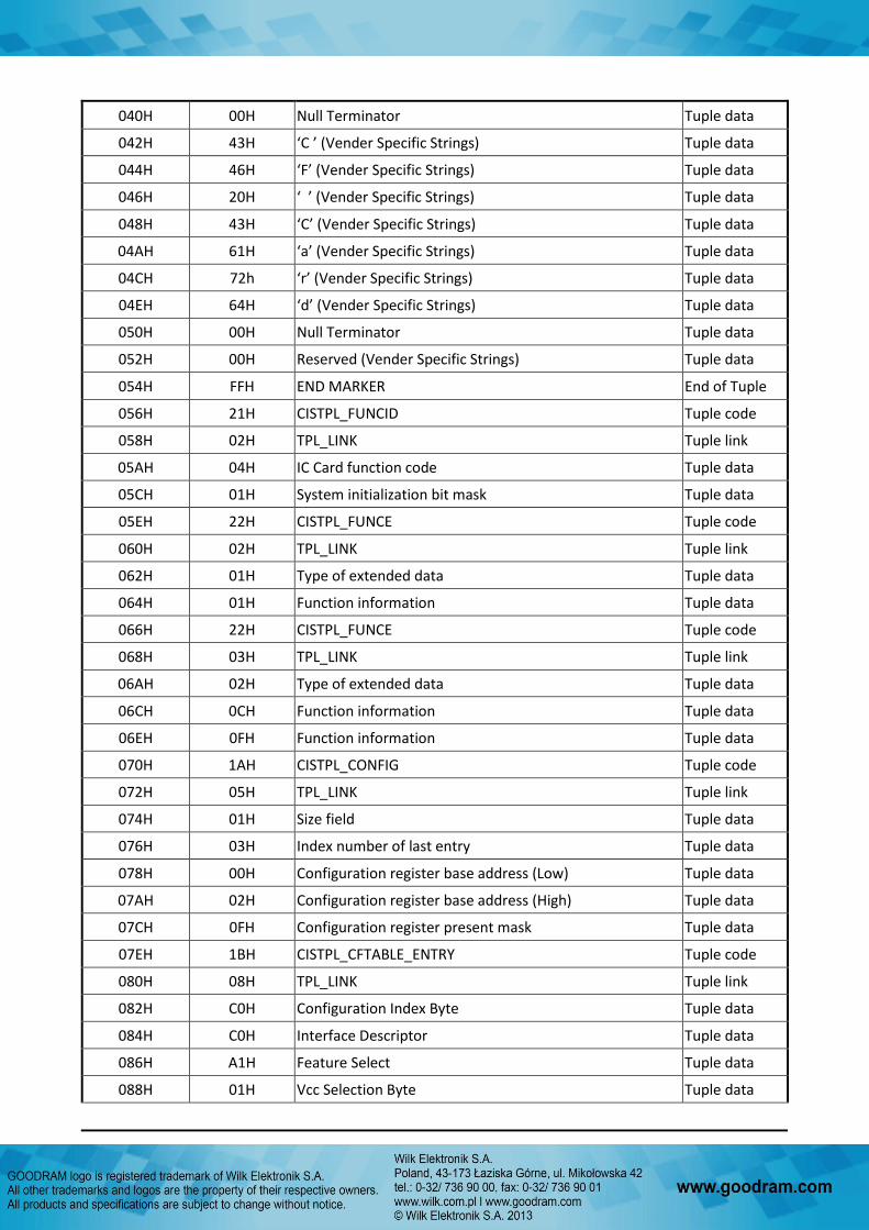
6. Power Management
CompactFlash provides automatic power saving modes, and the following are the descriptions which
address the conditions and reactions when a card enters a specific mode:
Standby Mode: When CF Card finishes the initialization routine after power reset, it goes
into Standby Mode and will wait for Command In or Soft Reset.
Active Mode: If CF Card receives any Command In or Soft Reset, it goes into Active Mode.
In Active Mode, CF card is capable of executing any ATA commands.
Therefore, power consumption is the greatest under this mode.
Idle Mode: After CF Card executes any ATA Commands or Soft Reset, it goes into Idle
Mode. Power consumption is reduced from Active Mode.
Sleep Mode: CF Card will enter Sleep Mode if there is no Command In or Soft Reset from
the host. Sleep Mode provides the lowest power consumption. During
Sleep Mode, the main clock of the system is stopped. Hardware reset,
software reset or any ATA command assertion will awake the controller
from Sleep Mode.
Power Saving Flow
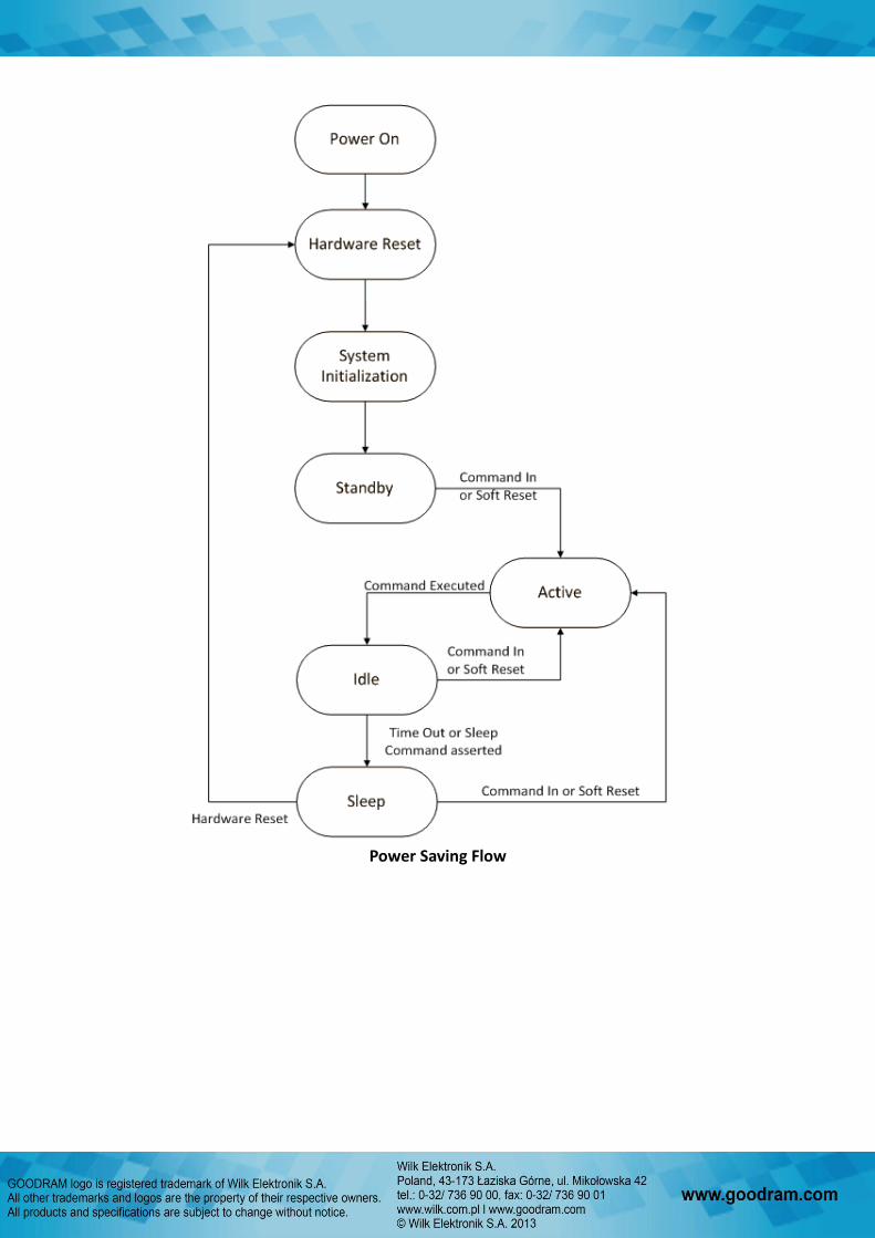
7. System Power Consumption Power Consumption
(Ta = 0 to 60º)
Symbol Parameters Conditions MIN TYP MAX Unit
Iccr Read current 5V - 80 - mA
Iccw Write current 5V - 110 - mA
Ipd
Power down current
(Commercial grade) 5V - - 0.4 mA
Power down current
(Extensive grade) 5V 0.6 mA
Iccr Read current 3.3V - 120 - mA
Iccw Write current 3.3V - 160 - mA
Ipd
Power down current
(Commercial grade) 3.3V - - 0.3 mA
Power down current
(Extensive grade) 3.3V 0.5 mA
8. Electrical Specifications Absolute Maximum Rating
Item Symbol Parameter MIN MAX Unit Remark
1 VDD-VSS DC Power Supply -0.3 +5.5 V
2 VIN Input Voltage VSS-0.3 VDD+0.3 V
3 Ta Operating Temperature 0 +70 °C Commercial Grade
4 Tst Storage Temperature -40 +85 °C Commercial Grade
5 Ta Operating Temperature -40 +85 °C Industrial Grade
6 Tst Storage Temperature -40 +85 °C Industrial Grade
Parameter Symbol Min TYP MAX Unit
VDD
Voltage VDD
3.0 3.3 3.6 V
4.5 5.0 5.5 V

9. DC Characteristics DC characteristics of 5.0V I/O Cells (Host Interface)
Symbol Parameter Conditions MIN TYP MAX Unit
Vol Output Low voltage |Iol| = 4 ~ 32 mA - - 0.4 V
Voh Output High voltage |Ioh| =4 ~ 32 mA 2.4 - - V
Rpu Input Pull-Up Resistance PU=high, PD=low 200 300 450 KΩ
Rpd Input Pull-Down Resistance PU=high, PD=low 200 300 450 KΩ
Iin Input Leakage Current Vin = VCC3I or 0 -10 ±1 10 μA
Ioz Tri-state Output Leakage
Current -10 ±1 10 μA

10. AC Characteristics
10.1. PCMCIA Interface
Attribute Memory Read Timing
Attribute Memory Read Timing
Speed Version Symbol IEEE Symbol
300 ns.
Item Min ns. Max ns.
Read Cycle Time tc(R) tAVAV 300
Address Access Time ta(a) tAVQV 300
Card Enable Access Time ta(CE) tELQV 300
Output Enable Access ta(OE) tGLQV 150
Output Disable Time from CE tdis(CE) tEHQZ 100
Output Disable Time from OE tdis(OE) tGHQZ 100
Address Setup Time tsu(A) tAVGL 30
Output Enable Time from CE ten(CE) tELQNZ 5
Output Enable Time from OE ten(OE) tGLQNZ 5
Data Valid from Address Change tv(A) tAXQX 0

Attribute Memory Write Timing
Attribute Memory Write Timing Speed Version
Symbol IEEE Symbol 250 ns
Item Min ns Max ns
Write Cycle Time tc(W) tAVAV 250
Write Pulse Width tw(WE) tWLWH 150
Address Setup Time tsu(A) tAVWL 30
Write Recovery Time trec(WE) tWMAX 30
Data Setup Time for WE tsu(D-WEH) tDVWH 80
Data Hold Time th(D) tWMDX 30

Common Memory Read Timing
Common Memory Read Timing Cycle Time Mode 250 ns 120 ns 100 ns 80 ns
Item Symbol IEEE
Symbol Min ns. Max ns. Min ns. Max ns. Min ns. Max ns. Min ns.
Max ns.
Output Enable Access Time
ta(OE) tGLQV 125 60 50 45
Output Disable Time from OE
tdis(OE) tGHQZ 100 60 50 45
Address Setup Time
tsu(A) tAVGL 30 15 10 10
Address Hold Time th(A) tGHAX 20 15 15 10
CE Setup before OE tsu(CE) tELGL 0 0 0 0
CE Hold following OE
th(CE) tGHEH 20 15 15 10
Wait Delay Falling from OE
tv(WT-OE)
tGLWTV 35 35 35 na1
Data Setup for Wait Release
tv(WT) tQVWTH 0 0 0 na1
Wait Width Time2 tw(WT) tWTLWTH 350(3000 for CF+)
350(3000 for CF+)
350(3000 for CF+)
na1
NOTES:
1. -WAIT is not supported in this mode. 2. The maximum load on –WAIT is 1 LSTTL with 50pF (40pF below 120nsec Cycle Time) total load.
All times are in nanoseconds. Dout signifies data provided by the CompactFlash Storage Card or CF+
Card to the system. The –WAIT signal may be ignored if the –OE cycle to cycle time is greater than the
Wait Width time. The Max Wait Width time can be determined from the Card Information Structure.
The Wait Width time meets the PCMCIA specification of 12us but is intentionally less in this
specification.

Common Memory Write Timing
Common Memory Write Timing
Cycle Time Mode 250 ns 120 ns 100 ns 80 ns
Item Symbol IEEE
Symbol Min ns. Max ns. Min ns. Max ns. Min ns. Max ns. Min ns.
Max ns.
Data Setup before WE
tsu(D-WEH)
tDVWH 80 50 40 30
Data Hold following WE
th(D) tWMDX 30 15 10 10
WE Pulse Width
tw(WE) tWLWH 150 70 60 55
Address Setup Time
tsu(A) tAVWL 30 15 10 10
CE Setup before WE
tsu(CE) tELWL 0 0 0 0
Write Recovery Time
trec(WE) tWMAX 30 15 15 15
Address Hold Time
th(A) tGHAX 20 15 15 15
CE Hold following WE
th(CE) tGHEH 20 15 15 10
Wait Delay Falling from WE
tv(WT-WE)
tWLWTV 35 35 na1
WE High from Wait Release
tv(WT) tWTHWH 0 0 0 na1
Wait Width Time2
tw(WT) tWTLWTH 350(3000 for CF+)
350(3000 for CF+)
350(3000 for CF+)
na1

NOTES:
1. –WAIT is not supported in this mode. 2. The maximum load on –WAIT is 1 LSTTL with 50 pF (40pF below 120nsec Cycle Time) total load. All
times are in nanoseconds. Din signifies data provided by the system to the CompactFlash Storage Card. The –WAIT signal may be ignored if the –WE cycle to cycle time is greater than the Wait Width time. The Max Wait Width time can be determined from the Card Information Structure. The Wait Width time meets the PCMCIA specification of 12us but is intentionally less in this specification.
I/O Read Timing
I/O Read Timing
Cycle Time Mode 250 ns 120 ns 100 ns 80 ns
Item Symbol IEEE
Symbol Min (ns.)
Max (ns.)
Min (ns.)
Max (ns.)
Min (ns.)
Max (ns.)
Min (ns.)
Max (ns.)
Data Delay after IORD td(IORD) tlGLQV 100 50 50 45
Data Hold following IORD
th(IORD) tlGHQX 0 5 5 5
IORD W idth Time tw(IORD) tlGLIGH 165 70 65 55
Address Setup before IORD
tsuA(IORD) tAVIGL 70 25 25 15
Address Hold following IORD
thA(IORD) tlGHAX 20 10 10 10
CE Setup before IORD tsuCE(IORD) tELIGL 5 5 5 5
CE Hold following IORD thCE(IORD) tlGHEH 20 10 10 10
REG Setup before IORD tsuREG (IORD)
tRGLIGL 5 5 5 5
REG Hold following IORD
thREG (IORD)
tlGHRGH 0 0 0 0
INPACK Delay Falling tdfINPACK tlGLIAL 0 45 0 na1 0 na1 0 na1

from IORD3 (IORD)
INPACK Delay Rising from IORD3
tdrINPACK (IORD)
tlGHIAH 45 na1 na1 na1
IOIS16 Delay Falling from Address3
tdfIOIS16 (ADR)
tAVISL 35 na1 na1 na1
IOIS16 Delay Rising from Address3
tdrIOIS16 (ADR)
tAVISH 35 na1 na1 na1
Wait Delay Falling from IORD3
tdW T(IORD)
tlGLW TL 35 35 35 na2
Data Delay from Wait Rising3
td(W T) tW THQV 0 0 0 na2
Wait Width Time3 tw(W T) tW TLW TH
350 (3000
for CF+)
350 (3000
for CF+)
350 (3000
for CF+)
na2
NOTES:
1. -IOIS16 and -INPACK are not supported in this mode. 2. -W AIT is not supported in this mode. 3. Maximum load on -WAIT, -INPACK and -IOIS16 is 1 LSTTL with 50 pF (40pF below 120nsec Cycle Time)
total load. All times are in nanoseconds. Minimum time from -WAIT high to -IORD high is 0 nsec, but minimum -IORD width shall still be met. Dout signifies data provided by the CompactFlash Storage Card or CF+ Card to the system. Wait Width time meets PCMCIA PC Card specification of 12µs but is intentionally less in this spec.
Figure 10-1: I/O Write Timing
Table 10-1: I/O Write Timing
Cycle Time Mode 255 ns 120 ns 100 ns 80 ns
Item Symbol IEEE
Symbol Min (ns.)
Max (ns.)
Min (ns.)
Max (ns.)
Min (ns.)
Max (ns.)
Min (ns.)
Max (ns.)
Data Setup before IOWR
tsu(IOW R) tDVIW H 60 20 20 15
Data Hold following IOWR
th(IOW R) tlWHDX 30 10 5 5
IOW R Width Time tw(IOW R) tlWLIW H 165 70 65 55
Address Setup before IOW R
tsuA(IOW R) tAVIW L 70 25 25 15
Address Hold following IOW R
thA(IOW R) tlWHAX 20 20 10 10
CE Setup before IOWR tsuCE (IOW R) tELIW L 5 5 5 5
CE Hold following IOWR
thCE (IOW R) tlWHEH 20 20 10 10
REG Setup before IOWR
tsuREG (IOW R)
tRGLIW L 5 5 5 5
REG Hold following IOWR
thREG (IOW R) tlWHRGH 0 0 0 0
IOIS16 Delay Falling from Address3
tdfIOIS16 (ADR)
tAVISL 35 na1 na1 na1
IOIS16 Delay Rising from Address3
tdrIOIS16 (ADR)
tAVISH 35 na1 na1 na1
Wait Delay Falling from IOW R3
tdW T(IOWR) tlWLW TL 35 35 35 na2
IOW R high from Wait High3
tdrIOW R (W T)
tW TJIWH 0 0 0 na2
Wait Width Time3 tw(W T) tW TLW
TH
350 (3000
for CF+)
350 (3000
for CF+)
350
(3000 for CF+)
na2

NOTES:
1. -IOIS16 and -INPACK are not supported in this mode. 2. -W AIT is not supported in this mode. 3. The maximum load on -WAIT, -INPACK, and -IOIS16 is 1 LSTTL with 50 pF (40pF below 120nsec Cycle
Time) total load. All times are in nanoseconds. Minimum time from -WAIT high to -IOWR high is 0 nsec, but minimum -IOW R width shall still be met. Din signifies data provided by the system to the CompactFlash Storage Card or CF+ Card. The Wait Width time meets the PCMCIA PC Card specification of 12 µs but is intentionally less in this specification.
10.2. IDE Interface Timing (PIO Mode)
ADDR valid
(A02, A01,
A00, -CS0, -
CS1, see
note 1)
-IORD/-IOWR
Write
Data(D15:D00)
(See note2)
-IOCS16
(See note3)
Read
Data(D15:D00)
(See note2)
-IORDY
(See note4, 4-1)
-IORDY
(See note4, 4-2)
-IORDY
(See note4, 4-3)
t0
t1 t2 t9 t8
t3 t4
t5 t6
t6z
t7
tA
tC
tRD
tB tC
t2i
IDE Interface Timing (PIO Mode)
NOTES:
1. Device address consists of -CS0, -CS1, and A[02:00]. 2. Data consists of D[15::00] (16-bit) or D[07::00] (8 bit). 3. -IOCS16 is shown for PIO modes 0, 1 and 2. For other modes, this signal is ignored. 4. The negation of IORDY by the device is used to extend the PIO cycle. The determination of whether
the cycle is to be extended is made by the host after tA from the assertion of -IORD or -IOWR. The assertion and negation of IORDY is described in the following three cases: Device never negates IORDY: No wait is generated. Device starts to drive IORDY low before tA, but causes IORDY to be asserted before tA: No wait
generated. Device drives IORDY low before tA: wait generated. The cycle completes after IORDY is reasserted.
For cycles where a wait is generated and -IORD is asserted, the device shall place read data on D15-D00 for tRD before causing IORDY to be asserted.

IDE Interface Timing
Name Item Mode0 Mode1 Mode2 Mode3 Mode4 Mode5 Mode6 Note
t0 Cycle time (min) 600 383 240 180 120 100 80 1
t1 Address Valid to -IORD/-IOWR setup (min)
70 50 30 30 25 15 10
t2 -IORD/-IOWR (min) 165 125 100 80 70 65 55 1
t2 -IORD/-IOWR (min) Register (8 bit)
290 290 290 80 70 65 55 1
t2i -IORD/-IOWR recovery time (min)
- - - 70 25 25 20 1
t3 -IOWR data setup (min) 60 45 30 30 20 20 15
t4 -IOWR data ho ld (min) 30 20 15 10 10 5 5
t5 -IORD data setup (min) 50 35 20 20 20 15 10
t6 -IORD data hold (min) 5 5 5 5 5 5 5
T6Z -IORD data tristate (max) 30 30 30 30 30 20 20 2
t7 Address valid to -IOCS16 assertion (max)
90 50 40 n/a n/a n/a n/a 4
t8 Address valid to -IOCS16 released (max)
60 45 30 n/a n/a n/a n/a 4
t9 -IORD/-IOWR to address valid ho ld
20 15 10 10 10 10 10
tRD Read Data Valid to IORDY active (min), if IORDY initially lo w after tA
0 0 0 0 0 0 0
tA IORDY Setup time 35 35 35 35 35 na5 na5 3
tB IORDY Pulse Width (max) 1250 1250 1250 1250 1250 na5 na5
tC IORDY assertion to release (max)
5 5 5 5 5 na5 na5
NOTES:
All timings are in nanoseconds. The maximum load on -IOCS16 is 1 LSTTL with a 50 pF (40pF below
120nsec Cycle Time) total load. All times are in nanoseconds. Minimum time from -IORDY high to -IORD
high is 0 nsec, but minimum -IORD width shall still be met.

1. t0 is the minimum total cycle time, t2 is the minimum command active time, and t2i is the minimum command recovery time or command inactive time. The actual cycle time equals the sum of the actual command active time and the actual command inactive time. The three timing requirements of t0, t2, and t2i shall be met. The minimum total cycle time requirement is greater than the sum of t2 and t2i. This means a host implementation can lengthen either or both t2 or t2i to ensure that t0 is equal to or greater than the value reported in the device’s identify device data. A CompactFlash Storage Card implementation shall support any legal host implementation.
2. This parameter specifies the time from the negation edge of -IORD to the time that the data bus is no longer driven by the CompactFlash Storage Card (tri-state).
3. The delay from the activation of -IORD or -IOW R until the state of IORDY is first sampled. If IORDY is inactive then the host shall wait until IORDY is active before the PIO cycle can be completed. If the CompactFlash Storage Card is not driving IORDY negated at tA after the activation of -IORD or -IOW R, then t5 shall be met and tRD is not applicable. If the CompactFlash Storage Card is driving IORDY negated at the time tA after the activation of -IORD or -IOW R, then tRD shall be met and t5 is not applicable.
4. t7 and t8 apply only to modes 0, 1 and 2. For other modes, this signal is not valid. 5. IORDY is not supported in this mode.
10.3. Multi Word DMA
-CS0,-CS1
DMARQ
DMACK
-IORD
-IOWR
Read Data
(D15:D00)
Write Data
(D15:D00)
tM
tN
t I tD tK tJ
tZtE
tFtG
tG
tH
tO
tL
Multi Word DMA
NOTES:
1. If the Card cannot sustain continuous, minimum cycle time DMA transfers, it may negate DMARQ within the time specified from the start of a DMA transfer cycle to suspend the DMA transfers in progress and reassert the signal at a later time to continue the DMA operation.
2. This signal may be negated by the host to suspend the DMA transfer in progress. All waveforms in this diagram are shown with the asserted state high. Negative true signals appear
inverted on the bus relative to the diagram.

MDMA Mode Timing Table
Item Mode 0 Mode 1 Mode 2 Mode 3 Mode 4 Note
Symbol (ns) (ns) (ns) (ns) (ns)
t0 Cycle time (min) 480 150 120 100 80 1
tD -IORD / -IOWR asserted width (min)
215 80 70 65 55 1
tE -IORD data access (max) 150 60 50 50 45
tF -IORD data hold (min) 5 5 5 5 5
tG -IORD / -IOWR data setup (min) 100 30 20 15 10
tH -IOWR data hold (min) 20 15 10 5 5
tI DMACK to -IORD/-IOWR setup (min)
0 0 0 0 0
tJ -IORD / -IOWR to -DMACK hold (min)
20 5 5 5 5
tKR -IORD negated width (min) 50 50 25 25 20 1
tKW -IOWR negated width (min) 215 50 25 25 20 1
tLR -IOWR to DMARQ delay (max) 120 40 35 35 35
tLW -IOWR to DMARQ delay (max) 40 40 35 35 35
tM CS(1:0) valid to -IORD/-IOWR 50 30 25 10 5
tN CS(1:0) hold 15 10 10 10 10
tZ -DMACK 20 25 25 25 25
NOTE: t0 is the minimum total cycle time and tD is the minimum command active time, while tKR and tKW are
the minimum command recovery time or command inactive time for input and output cycles
respectively. The actual cycle time equals the sum of the actual command active time and the actual
command inactive time. The three timing requirements of t0, tD, tKR and tKW shall be met. The
minimum total cycle time requirement is greater than the sum of tD, tKR and tKW for input and output
cycles respectively. This means a host implementation can lengthen either or both of tD and either of
tKR and tKW as needed to ensure that tD is equal to or greater than the value reported in the device’s
identify device data. A CompactFlash Storage Card implementation shall support any legal host
implementation.

10.4. Ultra DMA
(-)DMARQ
(device)
(-)DMACK
(host)
STOP
(host)
HDMARDY
(host)
DSTROBE
(device)
Data
D15:D00
A[02:00]
-CS0,-CS1(IDE),
-CE1,-CE2
(PC Card)
A[10:00]
(PC Card)
tUI
tACK
tACK
tACK
tZIORDY
tAZ
tENV
tENV
tZAD
tZAD
tFS
tFS
tZFS
tDZFS
tDVS tDVH
To Initialize an Ultra DMA Data in Burst Timing
DSTROBE
at device
Data
(D[15:00])
at device
DSTROBE
at host
Data
(D[15:00])
at host
t2CYC
tCYC
tDVS
tDVSIC
tDVS
tDVSIC
tDVH
tDVHIC
tDVH
tDVHIC
tDVH
tDVHIC
tCYC
tDH
tDHIC
t2CYC
tDH
tDHIC
tDH
tDHIC
tDS
tDSIC
tDS
tDSIC
Sustained Ultra DMA Data-in Burst Timing

Ultra DMA Mode Timing
UDMA Measure
Name Mode 0 Mode 1 Mode 2 Mode 3 Mode 4 Mode 5 Mode 6 Location
Min Max Min Max Min Max Min Max Min Max Min Max Min Max (See Note 2)
t2CYCTYP 240 160 120 90 60 40 30 Sender
tCYC 112 73 54 39 25 16.8 13 Note 3
t2CYC 230 153 115 86 57 38 29 Sender
tDS 15 10 7 7 5 4 2.6 Recipient
tDH 5 5 5 5 5 4.6 3.5 Recipient
tDVS 70 48 31 20 6.7 4.8 4 Sender
tDVH 6.2 6.2 6.2 6.2 6.2 4.8 4 Sender
tCS 15 10 7 7 5 5 5 Device
tCH 5 5 5 5 5 5 5 Device
tCVS 70 48 31 20 6.7 10 10 Host
tCVH 6.2 6.2 6.2 6.2 6.2 10 10 Host
tZFS 0 0 0 0 0 35 25 Device
tDZFS 70 48 31 20 6.7 25 17.5 Sender
tFS 230 200 170 130 120 90 80 Device
tLI 0 150 0 150 0 150 0 100 0 100 0 75 0 60 Note 4
tMLI 20 20 20 20 20 20 20 Host
tUI 0 0 0 0 0 0 0 Host
tAZ 10 10 10 10 10 10 10 Note 5
tZAH 20 20 20 20 20 20 20 Host
tZAD 0 0 0 0 0 0 0 Device
tENV 20 70 20 70 20 70 20 55 20 55 20 50 20 50 Host
tRFS 75 70 60 60 60 50 50 Sender
tRP 160 125 100 100 100 85 85 Recipient
tIORDYZ 20 20 20 20 20 20 20 Device
tZI ORDY 0 0 0 0 0 0 0 Device
tACK 20 20 20 20 20 20 20 Host
tSS 50 50 50 50 50 50 50 Sender

UDMA Measure
Name Mode 7 Location
Min Max (See Note 2)
t2CYCTY
P 24 Sender
tCYC 10 Note 3
t2CYC 23 Sender
tDS 2.5 Recipient
tDH 2.9 Recipient
tDVS 2.9 Sender
tDVH 3.2 Sender
tCS 5 Device
tCH 5 Device
tCVS 10 Host
tCVH 10 Host
tZFS 15 Device
tDZFS 10.5 Sender
tFS 70 Device
tLI 0 50 Note 4
tMLI 20 Host
tUI 0 Host
tAZ 10 Note 5
tZAH 20 Host
tZAD 0 Device
tENV 20 50 Host
tRFS 50 Sender
tRP 85 Recipient
tIORDYZ 20 Device
tZI
ORDY 0 Device
tACK 20 Host
tSS 50 Sender

Ultra DMA Data Burst Timing Descriptions
Name Comment Notes
t2CYCTYP Typical sustained average two cycle time
tCYC Cycle time allowing for asymmetry and clock variations (from STROBE edge to STROBE edge)
t2CYC Two cycle time allowing for clock variations (from rising edge to next rising edge or from falling edge to next falling edge of STROBE)
tDS Data setup time at recipient (from data valid until STROBE edge) 2, 5
tDH Data ho ld time at recipient (from STROBE edge until data may become invalid)
2, 5
tDVS Data valid setup time at sender (from data valid until STROBE edge) 3
tDVH Data valid ho ld time at sender (from STROBE edge until data may become invalid)
3
tCS CRC word setup time at device 2
tCH CRC word hold time device 2
tCVS CRC word valid setup time at host (from CRC valid until -DMACK negation) 3
tCVH CRC word valid hold time at sender (from -DMACK negation until CRC may become invalid)
3
tZFS Time from STROBE output released-to-driving until the first transition of critical timing.
tDZFS Time from data output released-to-driving until the first transition of critical timing.
tFS First STROBE time (for device to first negate DSTROBE from STOP during a data in burst)
tLI Limited interlock time 1
tMLI Interlock time with minimum 1
tUI Unlimited interlock time 1
tAZ Maximum time allowed for output drivers to release (from asserted or negated)
tZAH Minimum delay time required for output
tZAD drivers to assert or negate (from released)
tENV
Envelope time (from -DMACK to STOP and -HDMARDY during data in burst initiation and from DMACK
to STOP during data out burst initiation)
tRFS Ready-to-final-STROBE time (no STROBE edges shall be sent this long after negation of -DMARDY)
tRP Ready-to-pause time (that recipient shall wait to pause after negating -DMARDY)
tIORDYZ Maximum time before releasing IORDY 6
tZI ORDY Minimum time before driving IORDY 4, 6
tACK Setup and ho ld times for -DMACK (before assertion or negation)
tSS Time from STROBE edge to negation of DMARQ or assertion of STOP (when sender terminates a burst)
NOTES:
1. T he parameters tUI, tML I, and tLI indicate sender-to-recipient or recipient-to-sender interlocks, i.e.,
one agent (either sender or recipient) is waiting for the other agent to respond with a signal before proceeding. tUI is an unlimited interlock that has no maximum time value. tMLI is a limited time-out
that has a defined minimum. tLI is a limited time-out that has a defined maximum.
2. 80-conductor cabling shall be required in order to meet setup (tDS, tCS) and hold (tDH, tCH) times in
modes greater than 2. 3. Timing for tDVS, tDVH, tCVS and tCVH shall be met for lumped capacitive loads of 15 and 40 pF at
the connector where the Data and STROBE signals have the same capacitive load value. Due to reflections on the cable, these timing measurements are not valid in a normally functioning system.
4. For all timing modes the parameter tZIORDY may be greater than tENV due to the fact that the host
has a pull-up o n IORDY- giving it a known state when released. 5. T he parameters tDS and tDH for mode 5 are defined for a recipient at the end of the cable only in a
configuration with a single device located at the end of the cable. T his could result in the minimum values for tDS and tDH for mode 5 at the middle connector being 3.0 and 3.9 ns respectively.
6. T his parameter applies to True IDE mode operation only.

11. Package Specifications
12. LBA and CHS Parameters
LBA and CHS Parameters per Capacity
Capacity LBA CHS
Cylinders Head Sector
1GB 1883952 1869 16 63
2GB 3767904 3738 16 63
4GB 7535808 7476 16 63
8GB 15072624 14953 16 63
16GB 30146256 16383 16 63
32GB 61078752 16383 16 63
64GB 122158512 16383 16 63
Notes:
1. Date is tested by Toshiba 24nm SLC/19nm MLC Flash.
2. Value may vary from flash configuration.

Warning • Do not bend, crush, drop, or place heavy objects on top of the Product. Do not use tweezers, pliers, or similar items that could damage the Product. Take particular care when inserting or removing the Product. Stop using the Product when the Product does not work properly. Failure to follow these instructions could result in fire, damage to the Product and/or other property, and/or personal injury including burns and electric shock. • Keep out of reach of small children. Accidental swallowing may cause suffocation or injury. Contact a doctor immediately if you suspect a child has swallowed the Product. . • Do not directly touch the interface pins, put them in contact with metal, strike them with hard objects, or cause them to short. Do not expose to static electricity. • Do not disassemble or modify the Product. This may cause electric shock, damage to the Product, or fire.
Notes on usage • The Product contains nonvolatile semiconductor memory. Do not use the Product in accordance with a method of usage other than that written in the manual. This may cause the destruction or loss of data. • To protect against accidental data loss, you should back up your data frequently on more than one type of storage media. **** Corporation assumes no liability for destruction or loss of data recorded on the Card for any reason. • When used over a long period of time or repeatedly, the reading, writing and deleting capabilities of the Product will eventually fail, and the performance speed of the Product may decrease below the original speed specific to the Product's applicable class. • If the Product is to be transferred or destroyed, note that the data it contained may still be recoverable unless it is permanently deleted by third-party deletion software or similar means beforehand.
Product applications and design.
Product is intended for use in general electronics applications (e.g., computers, personal equipment, office equipment, measuring equipment, industrial robots and home electronics appliances) or for specific applications as expressly stated in this document. Product is neither intended nor warranted for use in equipment or systems that require extraordinarily high levels of quality and/or reliability and/or a malfunction or failure of which may cause loss of human life, bodily injury, serious property damage or serious public impact (“Unintended Use”). Unintended Use includes, without limitation, equipment used in nuclear facilities, equipment used in the aerospace industry, medical equipment, equipment used for automobiles, trains, ships and other transportation, traffic signaling equipment, equipment used to control combustions or explosions, safety devices, elevators and escalators, devices related to electric power, and equipment used in finance-related fields. Do not use Product for Unintended Use unless specifically permitted in this document.
No parts of this document may be reproduced , stored in a retrieval system, or transmitted, in any form or by any
means, mechanical ,electric, photocopying, recording or otherwise, without permission of Wilk Elektronik S.A. Wilk Elektronik S.A does not make any warranty ,express or implied, with respect to this document, including as to licensing, Non-infringement , merchantability or fitness for a particular purpose.