GN001 Application Guide Design with GaN Enhancement …€¦ · GN001 Application Guide Design with...
46
GaN Systems –1 GN001 Application Guide Design with GaN Enhancement mode HEMT Updated on Oct-7-2016 GaN Systems Inc.
Transcript of GN001 Application Guide Design with GaN Enhancement …€¦ · GN001 Application Guide Design with...

GaN Systems – 1
GN001 Application GuideDesign with GaN Enhancement mode HEMT
Updated on Oct-7-2016GaN Systems Inc.

GaN Systems – 2
GaN has extremely fast switching speed and excellent reverse recovery performance. GaN Systems offers high performance and easy to use GaN true Enhancement mode
HEMT (E-HEMT) in embedded package.
Very high switching speed combined with some unique characteristics of GaN requires special attention to the gate drive circuit and layout design.
Abstract: This application guide highlights the basic characteristics of GaN Systems GaN E-HEMTs,
then the key design consideration of gate drive circuit and layout will be discussed followed by design examples.
Most of the discussion will be focused on 650V GaN, though many basic design principles apply to 100V GaN design as well.
Overview
GaN Systems – 3
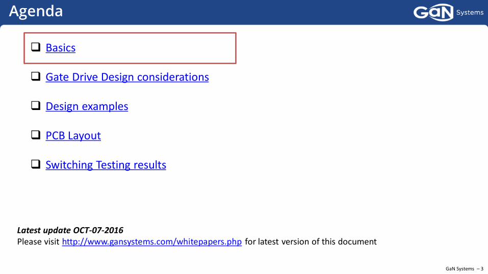
Agenda
Latest update OCT-07-2016Please visit http://www.gansystems.com/whitepapers.php for latest version of this document
Basics
Gate Drive Design considerations
Design examples
PCB Layout
Switching Testing results

GaN Systems – 4
Fundamentals
GaN Enhancement mode High Electron Mobility Transistor (E-HEMT) Lateral 2-dimensional electron gas (2DEG) channel formed on AlGaN/GaN hetero-
epitaxy structure provides very high charge density and mobility For enhancement mode operation, a gate is implemented to deplete the 2DEG
underneath at 0V or negative bias. A positive gate bias turns on the 2DEG channel
Si Substrate
GaN Buffer Layers
AlGaN Barrier Layer
Source Gate Drain
2DEG
0V
+-VDS
Si Substrate
GaN Buffer Layers
AlGaN Barrier Layer
Source Gate Drain
2DEG
+-VDS
VGS
IDS
IDS vs. VDS characteristics
VGS = 2V
VGS = 3V
VGS = 4V
VGS = 5V
VGS = 6VIDS (A)
VDS (V)

GaN Systems – 5
E-HEMT Gate characteristics
Gate Bias LevelGaN Systems GaN E-HEMT Si MOSFET IGBT SIC MOSFET
Maximum rating -10/+7V +/-20V +/-20V -8/+20V
Typical gate bias values 0 or-3/+5-6V 0/+10-12V 0 or -9/+15V -4/+15-20V
Common with Si MOSFET
True e-mode normally off Voltage driven - driver charges/discharges CISS
Supply Gate leakage IGSS only Easy slew rate control by RG
Differences
Much Lower QG : Lower drive loss; faster switching Higher gain and lower VGS : +5-6V gate bias to turn on Lower VG(th): typ. 1.5V
Vs other e-mode GaN
More robust gate: +7/-10V DC max rating No DC gate drive current required No complicated gate diode / PN junction
RG,extCGD
CGS
RG,int CDSGate
Drain
SourceCISS = CGD+CGS

GaN Systems – 6
Reverse recovery performanceGaN E-HEMT does not have parasitic body diode, thus No QRR, only QOSS lossBut it is naturally capable of reverse conduction without external anti-parallel diodeGaN is good fit for half bridge hard switching application
Si MOSFET
IDS
Qrr_mea = Qrr_diode + QOSS
Trr
Irr
dirr1/dtta tb
dirr2/dt
Qrr_diode
Incl. Qoss
Qrr
Loss
Qoss
Loss
V/I
loss
VDS
IDiodeIDS_Q2
Qoss
Loss
V/I loss
Qoss
VDS
IDS_Q1
di1/dt di2/dt
ipk
Qrr_mea = Qoss
GaN QOSS vs Si MOSFET QRR: Order of magnitude smaller than QOSS
QRR changes with di/dt and TJ while QOSS is a fixed value
Similar IDS overshoot caused by charging high side COSS
No QRR loss period di2/dt can be controlled (turn-on di/dt and LC
resonance), No uncontrolled snappy recovery issue
GaN E-HEMT
QRRQOSS
650V SJ MOSFET QRR = 1000 – 10000nC!
650V GaNQOSS = 60nC
GaN Systems – 7
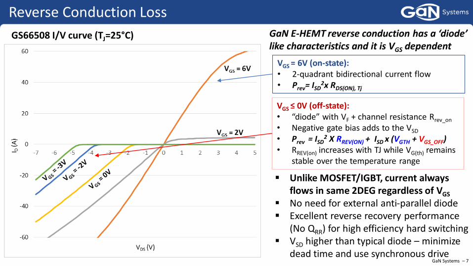
Reverse Conduction LossGaN E-HEMT reverse conduction has a ‘diode’ like characteristics and it is VGS dependent
GS66508 I/V curve (TJ=25°C)
VGS = 6V (on-state):• 2-quadrant bidirectional current flow• Prev= ISD
2x RDS(ON), Tj
VGS ≤ 0V (off-state):• “diode” with VF + channel resistance Rrev_on
• Negative gate bias adds to the VSD
• Prev = ISD2 X RREV(ON) + ISD x (VGTH + VGS_OFF)
• RREV(on) increases with TJ while VG(th) remains stable over the temperature range
Unlike MOSFET/IGBT, current always flows in same 2DEG regardless of VGS
No need for external anti-parallel diode Excellent reverse recovery performance
(No QRR) for high efficiency hard switching VSD higher than typical diode – minimize
dead time and use synchronous drive

GaN Systems – 8
Setting up dead time
VGSH
VGSL
For hard switching: td_pwm must be > tdelay_skew + (td(off) - td(on)):
Gate turn-on/off delay difference varies with RG: typical +/-5ns range (GS66508) High/low side gate driver delay skew (worst case delay mismatch) usually dominates:
Example Silab Si8261 isolated gate driver tdelay_skew_max = 25ns. In this case the dead time must be set > 30ns as minimum
However in practical circuit safety margin must be considered: for GS66508 typical 50-100ns is chosen for dead time
For soft switching dead time needs to be chosen for achieving ZVS transition For 100V: smaller can be used (15-20ns) as 100V driver has better delay matching
Actual dead time
Td_actual ~= td_pwm - tdelay_skew - td(off) + td(on)
PWM signal dead time td_pwm
VGS_Q1 VGS_Q2
VDStd(off) td(on) tr

GaN Systems – 9
Agenda
Basics
Gate Drive Design considerations
Design examples
PCB Layout
Switching Testing results

GaN Systems – 10
Design Considerations – fast switchingGaN can switch faster than Si/SiC MOSFETs with dv/dt > 100V/ns
VGS
GaN E-HEMT GS66508T
(650V/50mΩ)
Cree SiC C3M006509D (900V/
65mΩ)
Vgs=12V/-3V (SiC)
Vgs=6V/-3V (GaN E-HEMT)
VDS=400V
4.5ns (90V/ns)17ns (18V/ns)
Double Pulse Test Hard Switch Turn-on
(VDS=400V, ID=15A, RG(ON)=10Ω)
GaN shows 4x faster turn-on and ~2x faster off time than state of art SiC MOSFET with similar Rds(on) Care should be taken when designing with such a high switching speed and dv/dt
VDS=400V
GaN E-HEMT SiC
Vgs=12V/-3V (SiC)
Vgs=6V/-3V (GaN E-HEMT)
Hard Switching Turn-off (VDS = 400V, ID = 15A, RG(OFF)=1Ω)
5.7ns10ns

GaN Systems – 11
Design Considerations
Design considerations for driving high speed GaN E-HEMTs:
Controlling noise coupling from power to gate drive loop should be the first priority:
High dv/dt and di/dt combined with low CISS and VG(th) → Need to protect gate spikes from going above threshold or maximum rating under miller effect for safe operation
Gate ringing or sustained oscillation may occur if the design is not done properly and may lead to device failure. We will discuss how to mitigate that in this section
On the other hand, the switching performance of GaN should not be compromised too much
This is more critical for 650V hard switching half bridge application as very high dv/dt could occur at hard turn-on.
Single end topology has less concern with miller effect, and for resonant ZVS topology the dv/dt and di/dt are lower so their design requirement may be relaxed.
In this section we will walk through the design tips on how to control miller effect and mitigate gate ringing/oscillation, followed by gate driver recommendations

GaN Systems – 12
Gate drive impedance (Rg and Lg) is critical for turn-off, but less at turn-onBasic rule: the gate needs to be held down as strong as possible with minimum impedanceMiller effect is more prominent at 650V than 100V design due to the higher dv/dt
Control miller effect
CGD
CDS
CGS
RGLG
LD
LCS
LS
imillerROL
VDS
VGS
Positive dv/dt
Prevent false turn-on Strong pull-down (low RG/ROL) Low LG to avoid ringing Use negative gate bias, -2 to -3V
is recommended
Negative dv/dt
CGD
CDS
CGS
RGLG
LD
LCS
LS
imillerROL
VDS
VGS
VGS-_pk
VGS+_pk
Occurs at turn-on of the complementary switch in half bridge
Keep VGS-_pk within -10V Strong pull-down (low RG/ROL) and low LG for lower ringing VGS may bounce back >0V (LC ringing): ensure VGS+_pk < VG(TH)
to avoid false turn-on or gate oscillation

GaN Systems – 13
Control miller effect For negative dv/dt, it is important to have a low-Z path for the reverse miller current to reduce the
negative VGS spike (and the ringing afterwards caused by LC resonance) Pay attention to the VGS spike around VDS <50V due to the change of non-linear CISS/CRSS ratio A clamping diode is recommended for gate drive with single output. For gate drive with separate
sink output the diode may not be needed depending on the RG and LG in the circuit For bipolar gate bias, use a TVS diode in series with the clamping diode (or two back to back) CGS may not help in some cases, be careful! ( induce LC resonance with Lgate and LCS) Negative gate bias can help to prevent false turn-on, but ensure worst case Vgs-_pk within -10V
VGS
-3V
6V
VDS
-7V
High dv/dt when the other switch is being turned on
<0V
RON=20Wwith DCLAMPRON=20W, no DCLAMP
-13V -2V VO+
RGON
RGOFF
Gate
DriverG
D
SVEE
VO-
VDD
-3V
+6V
DZ1
3V3
D2
VO
RGON
RGOFF D1
Gate
Driver
GND
Dclamp
CGD
CGS
LCS
0V

GaN Systems – 14
Control miller effect
Select right gate resistor GaN E-HEMT speed can be easily controlled by gate resistors Critical to choose the right RG(ON)/RG(OFF) ratio for performance and drive
stability Separate RG for turn-on and off is recommended Recommend RG(ON)/RG(OFF) ≥ 5-10 ratio for controlling the miller effect GaN has extremely low Qg and drive loss: most cases 0402/0603 SMD
resistors can be used Turn on RG(ON):
Control the turn-on dv/dt slew rate Too high RG(ON) slows down switching and increases loss Too small RGON: High dv/dt -> Higher switching loss due to the
miller turn-on and potential gate oscillation For GS66508: recommend to start with RG(ON) = 10-20Ω
Turn off RG(OFF): Typical starting value range is 1-2Ω Provide strong and fast pull-down for robust gate drive
VO
RGON
RGOFF D1
Low Vf Schottky Diode
Gate
DriverG
D
SGND
VO+RGON
RGOFF
Gate
DriverG
D
SGND
VO-
Gate driver w/ single output
Gate driver w/ separate outputs
(Preferred)

GaN Systems – 15
Mitigate gate ringing/oscillationsWhat causes the gate ringing/oscillation? Gate over/undershoot and ringing caused by high LG
Common Source Inductance LCS Feedback path from power to gate loop (di/dt) Capacitive coupling via miller capacitor CGD (dv/dt)
What to do if gate ringing/oscillation occurs? First improve the layout by reducing LG, LCS and external G-D coupling:
Locate driver as close to gate as possible Low inductance wide PCB trace and polygon Use kelvin source connection to minimize LCS
Select right RG to tune turn-on slew rate Try negative gate bias (-3V) for turn-off At last resort try circuits below to damp the high frequency LC ringing &
overshoot: Use a ferrite bead with Z=10-20Ω@100MHz in series with gate. (ferrite
bead may increase LG but damp the high frequency gate current ringing) RC snubber across G-S: example R=3.3/C=200-470pF
CGD
CGS
RGLG
LD
LCS
LS
RG1
LCS
FB1
Z=10-20
RG1
LCS
LG
RS1
CS1
3.3
100-200pF

GaN Systems – 16
High side driver considerations
GaN enables fast switching dv/dt >100kV/us: Minimize Coupling capacitance CIO
CM current via CIO limits CMTI Use isolator/isolated gate driver with high CMTI
Full Isolated gate drive: Best performance Isolation power supply – Minimize inter-winding
Capacitance Bootstrap:
Common for lower voltage 100V half bridge design Lower cost and simpler circuit Choose the bootstrap diode with low CJ and fast
recovery time. Watch for bootstrap diode power loss limit and recovery time for high-frequency operation.
Post-regulation or voltage clamping may be required after bootstrap
High side gate drive
IsolatorPWM
D
G
S
Isolated DC/
DC
Gate Driver
RG_ON
RG_OFF
VCC
0V
0VGDH
VCM
0V
ICM
High side floating ground VCM
CIO
CIO
ICM
ICM
Isolated DC/
DC
VCC
High side floating ground
CIO
ICM
Optional common mode choke at input side to suppress CM noise

GaN Systems – 17
Bootstrap circuit Good for low cost 0-6V gate drive, need additional offset circuit for bipolar drive What is the problem with traditional bootstrap circuit?
GaN E-HEMT requires good regulation of gate bias (5-6V bias, max rating 7V) LS free wheeling: Switch node negative voltage overcharges bootstrap capacitors (VGS>7V) HS free wheeling: Bootstrap diode voltage drops reduces VGS below 6V
Post-regulation or voltage clamping to ensure high side bias <7V
Bootstrap with post-regulation using +9V for regulated high side bias
+9V
0V
DB1
+6V
1K
DZ1 C1
5.8V
0VGDH
CB1
+9V
0V
DB1
+6V
C1
0VGDH
CB1
R1LP2985IM5-6.1
IN OUT
GND
D
G
S
Q1Gate
Driver
RG_ON
RG_OFF
D
G
S
Q2Gate
Driver
RG_ON
RG_OFF
+6V
0VIsolator
DBS
0VGDH
CBOOT
0VGDH
PWM_H
VDRVH
PWM_L
VBUS+
GND
-2 ~ -2.5V
0V
0.6V
VOUT
+
-
VSD
Can be over-charged to 7-9V Bootstrap for Sync Buck (only need to clamp overcharge, example 100V sync buck)
+6V
0V
DB1DZ1 C1
5.8V
0VGDH
VDRV
Simple Zener diode to clamp to 6V
Use LDO to regulate to 6V
Use Zener diode

GaN Systems – 18
Criteria for selecting GaN E-HEMT gate drivers
Choose gate driver with VDD and UVLO range that is compatible with 5-6V gate drive: For 0-6V drive bias: use UVLO ≤ 4-5V (designed for 5V FET gate drive) For -3/+6V bipolar drive: use driver designed for 9V gate drive (UVLO < 8V)
Low pull-down resistance and high sink current to minimize miller effect: Recommend ≥ 4A sink current (turn-on peak current requirement can be relaxed) Low pull-down resistance, Separate pull-up and down output pins preferred
Isolated gate driver: dv/dt CMTI rating: at minimum 50kV/us, preferred ≥100kV/us Propagation delay matching: It affects the minimum dead time for half bridge. At
minimum isolated driver with <100ns delay matching should be used, preferred <50ns Capable of high frequency operation: Fsw ≥ 1MHz 100V half bridge driver for GaN:
All above except isolation. Typically 100V driver is non-isolated with bootstrap. Voltage clamping or regulation is required after bootstrap
≥ 1-2MHz operation with tightly matched propagation delay matching (≤20ns)

GaN Systems – 19
Gate driver recommendation
For 650V GaN half bridge (Totem pole PFC/LLC/Full bridge/Inverter): SiLab Si827x series (high CMTI >200kV/us, low UVLO for 6V), recommended P/N:
Single channel Si8271 (single w/ split output) Half bridge Si8273/4/5 (HS&LS, PWM with DT Adj or dual) Use 3V UVLO version (XX-GB) for unipolar 6V gate bias. For +6/-3V bipolar drive either 3V or 5V
UVLO (XX-AB) version can be used
Analog device half bridge driver ADuM4223A/B (footprint compatible with Si8273/4)
For non-isolated low side application (Flyback, Class E PA, Boost, SSSR), 100V or 650V Taxes Instruments LM5114/UCC27511/Maxim MAX5048C (footprint compatible) Can also be used with isolator for high side drive, or as secondary gate drive for adapting existing 12-
15V gate driver Other verified low side drivers: FAN3122, FAN3224/5 (dual), LTC4441/MCP1407/IXDN609SI/TC4422
100V half bridge (48V-12V Sync Buck, Inverter, Class D PA) TI LM5113 (5V VCC) Linear Tech LTC4444-5 (Synchronous MOSFET driver, 5-6V VCC) Linear Tech LTC3895 (Sync. Step-down DC/DC controller)

GaN Systems – 20
Agenda
Basics
Gate Drive Design considerations
Design examples
PCB Layout
Switching Testing results

GaN Systems – 21
650V GaN Gate Drive Design – Unipolar gate driveFully isolated unipolar drive based on Si8271GB-IS Pros: Simple implementation, low dead time reverse conduction loss Cons: More sensitive to layout patristics compared to bipolar drive, gate drive layout and turn-on speed
needs to be optimized for hard switching topology. Optional ferrite bead (use 10-20Ω@100mhz) and clamping diode for gate spikes/ringing
U3
SI8271GB-IS
VI1
VDDI2
GNDI3
EN4
GNDA5
VO-6
VO+7
VDD8
Q4
GS66508B
1
2
4
3
GND_GD
R2
20R
R3
2R
D1
DNP
C3
2.2uF
FB1
0R
C5
1uF
GND_GD
R44.7K
PS1
PES1-S5-S9-M
GND1
VIN2
+VO5
0V4
NC
8
+9VISO
U1
LP2985IM5-6.1IN
1
GN
D2
ON/OFF3
BYP4
OUT5
GND_GD
C24.7uFC0805
0V
GND_GD
+5V
C14.7uFC0805
VDD_6V
R12.2KR0805
VDDH_6V
SOURCE
DRAIN
+5V
C40.1uF
0V
PWM_IN
EN
ISOLATION
Applications: Good for high frequency ZVS
application (no hard switching, lower dv/dt but dead time conduction loss is more critical)
Application with tight optimum gate drive layout (lower power)

GaN Systems – 22
650V GaN Gate Drive Design – Bipolar gate drive Fully isolated bipolar drive based on Si8271AB-IS Pros: Lower risk of cross conduction/gate oscillation, faster turn-on (lower switching loss), higher UVLO
drivers can be used for GaN Cons: higher dead time reverse conduction loss (minimize dead time), it is a trade off between switching
and dead time loss Use DZ1/R2 to split 9V to +6/-3V and create a biased gate return. No additional LDO is required as
negative bias voltage regulation can be more relaxed
U1
SI8271AB
VI1
VDDI2
GNDI3
EN4
GNDA5
VO-6
VO+7
VDD8
VCC
R810K
C7
1uF
GND_GD
C5
1uF
GND_GD
R3
10RR4
2R
Q1
GS66508T/16T
1
24
3
PS1
ISO DC/DC
GND1
VIN2
+VO5
0V4
NC
8
C34.7uFC0805
0V
VCC
C14.7uFC0805
R12.2KR0805
VDD
0V
C60.1uF
PWM_IN
EN
ISOLATION
DRAIN
SOURCE
DZ1
5V8
R21K
GD_GND
C21u
VDD
C41u
VEE
VEE
GD_GND
Applications: Applications where tight gate layout is
difficult due to PCB and thermal design Hard switching with relatively lower
FSW where switching loss dominates and dead time loss is less critical

GaN Systems – 23
650V GaN Gate Drive Design – Bias offset circuitOffset circuit to generate +6/-3V from single 9V bias (isolated grounds) With single end isolated 9V supply (return isolated from power ground ), you can use this bias offset
circuit to easily create -3V bias After startup, C11 will be charged by VDD and R13 until clamped by DZ1
U2
SI8271AB-IS
VI1
VDDI2
GNDI3
EN4
GNDA5
VO-6
VO+7
VDD8PWM_IN R7
10R
ENABLE
R8
10
VDD_9V
C71uF
0V
GND_GD
VCC_+5V
R9
1
GATEQ2
GS66508T
1
24
3
R1110k
TVS2
MMBZ5V6ALT1GSOT-23-3
D2
SOD-123F20V 1A
SOURCE
GND_GD
PS2
PES1-S5-S9-M
GND1
VIN2
+VO5
0V4
NC
8
VDRV
0V
VDD_9V
C94.7uFC0805
R123.3KR0805
C104.7uFC0805
DZ1
3V3C11
1uF
R133.3k
VDD_9V
C6
1uF
GaN Systems – 24
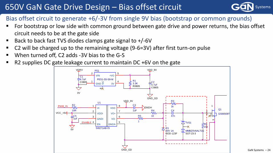
650V GaN Gate Drive Design – Bias offset circuitBias offset circuit to generate +6/-3V from single 9V bias (bootstrap or common grounds) For bootstrap or low side with common ground between gate drive and power returns, the bias offset
circuit needs to be at the gate side Back to back fast TVS diodes clamps gate signal to +/-6V C2 will be charged up to the remaining voltage (9-6=3V) after first turn-on pulse When turned off, C2 adds -3V bias to the G-S R2 supplies DC gate leakage current to maintain DC +6V on the gate
U1
SI8271AB-IS
VI1
VDDI2
GNDI3
EN4
GNDA5
VO-6
VO+7
VDD8
GNDHR2
10R
PWM_IN
ENABLE
R4
10
C3
1uF
VDD_9V
C51uF
VCC_+5V
0V
GND_GD
R5
1
C4
47n
R3
1k
Q1
GS66508T
1
24
3
R610k
TVS1
MMBZ5V6ALT1GSOT-23-3
D1
SOD-123F20V 1A
GND_GD
PS1
PES1-S5-S9-M
GND1
VIN2
+VO5
0V4
NC
8
0V
VDRV
C14.7uFC0805
VDD_9V
R13.3KR0805
C24.7uFC0805

GaN Systems – 25
650V GaN Gate Drive Design – non-isolated bootstrap Non-isolated bootstrap circuit is preferred for cost sensitive design Based on half bridge driver Si8273 (or Adum4223)
U3
SI8273GB / ADUM4223
VIA1
VIB2
VDDI3
GNDI4
DISABLE5
DT6
NC17
VDDI_28
GNDB9
VOB10
VDDB11
NC212
NC313
GNDA14
VOA15
VDDA16
VGDL_+6V
D6
600VES1J C8
1uF 25V
R121RR0805
C9
1uF 25V
C14
2.2uF 25V 0V
0V
VCC_+9V VGDH_+6V
0V_GDH
0V_GDH0V_GDH C11
2.2uF 25V
0V_GDH
VCC_+5V
R13 100R
R16 100R
R1420
VDC-
VDC+
R151 D7
PWMH
EN
PWML
PLACE U2 PIN.5 CLOSE TO C5
VSW
U2
LP2985IM5-6.1IN
1
GND
2
ON/OFF3
BYP4
OUT5
C1010nF
U4
LP2985IM5-6.1IN
1
GND
2
ON/OFF3
BYP4
OUT5
C1710nF
FB1
0
FB2
0
0V_GDH
Q3
GS66508B
1
2
4
3
Q4
GS66508B
1
2
4
3
R1720
R181 D8
DZ15V8
0V
DZ25V8
C16
1uF 25V
0V
VCC_+9V
0V0V
C13dnp
C15dnp
C12
0.1uF 25V
VCC_+5V
0V

GaN Systems – 26
650V GaN Gate Drive Design – non-isolated bootstrap Non-isolated bootstrap with half bridge gate driver 9V VDD with bias offset circuit for +6/-3V
U1
SI8273AB / ADUM4223B
VIA1
VIB2
VDDI3
GNDI4
DISABLE5
DT6
NC17
VDDI_28
GNDB9
VOB10
VDDB11
NC212
NC313
GNDA14
VOA15
VDDA16
C5
1uF
R9
10
R11
1
R1010K
Q2_KS
Q2_G
0V
D520V/1ASOD-123F
D4
20V/1ASOD-123F
C1
1uF
R8
1k
C6
47n
R1
3.3R0805
TVS2
MMBZ5V6ALT1GSOT-23-3
C2
1uF
VDD_+9V
0V
VGDH_+9V
0V_GDH
VCC_+5V
R6 100
R7 100
VDC+
VDC-
PWMH
PWML
EN
VSW
R3
10
R5
1
R410K
Q1_G
Q1_KS
0V_GDH
VDD_+9V
Q1
GS66508T/GS66516T
1
24
3
Q2
GS66508T/GS66516T
1
24
3
C71uF
VGDH_+9V
D1
ES1J
D320V/1ASOD-123F
D2
20V/1ASOD-123F
C4
0.1uF 25V
VCC_+5V
0V
R2
1k
C3
47n
PGND
TVS1
MMBZ5V6ALT1G
SOT-23-3

GaN Systems – 27
650V GaN gate drive design ideas
100n
G
S
D
VSS
Lcs1
3V3
GATE
VEE
0V
IGBT/MOSFET Driver
100R
VDD
R1
+15V
12-15V
VDD
PWM
Local driver on the power board
for low Lg
Iso. DC/DC
12-15V0V
RG1
VEE
100R
R2
D1
+9V
VSS
kS
+9V
R1
DZ1C1
C2
DZ2
DZ3
R3
3K3
R410K
9V
5.6V
5.6V
DZ4
IN
VDD
VSS
VO+
VO-RG2
IGBT/MOSFET drivers located at
distance
LM5114
Lg
Lg
Use secondary local driver for adapting IGBT/MOSFET gate drive signals Provide local optimum gate drive layout excluding high LG and LCS
Allows longer distance between GaN and controller/driver for control/power board(module) design The isolated IGBT/MOSFET driver needs to be able to handle high CMTI dv/dt (>50kV/us, 100kV/us
preferred)
You can also use totem pole emitter-follower buffer stage such as ZXGD3006E6

GaN Systems – 28
100V half bridge design example
U1
LM5113_DSBGA
DSBGA-12
VDD
HB
HOH
HOL
HS
VSS
LI
HI
LOL
LOH
R1
4R7
R0402
Q1
GS61004B
1
2
3
Q2
GS61004B
1
23
R2
4R7
R0402
PWML
PWMH
C1
0.1uC0402
HS
VDC+
0V
C21u
C0402
VCC
GS61004B Half bridge using LM5113 for 48V DC/DC Discrete design compared to other integrated GaN module:
Comparable device performance Similar PCB area (~49mm2 including 2x GS61004B.
LM5113 and R1/R2, excl. C1/C2) Better thermal performance than integrated solution
4.6mm
9mm~2.7mm
~2.7mm
GS61004B
GS61004B
LM5113

GaN Systems – 29
Agenda
Basics
Gate Drive Design considerations
Design examples
PCB Layout
Switching Testing results

GaN Systems – 30
PCB Layout Checklist
Design for GaNPx embedded package
GaNPx bottom cooled B/P
GaNPx Top cooled
Thermal design
Optimize and minimize layout parasitics in following orders :
1. Common source / mutual inductance LCS
2. Gate loop inductance LG
3. Power Loop inductance Lloop
4. Drain to gate loop capacitance CGD_ext
5. Isolation coupling capacitance CISO
LD1
LCS1
Q1
LP1
LG1 RG1
LG2
LD2
LCS2
Q2LG3 RG1
LG4
LP2
Gate
Driver
Gate
Driver
LS1
LS2
CGD_ext1
CGD_ext2
CDC_LINK
LLoop
0V
0V
CISO LM1
LM1

GaN Systems – 31
GaNPX™: Bottom cooled B type family
Top side Bottom side
S
SS G
0.5mm
Embedded package with extremely low inductance GS66508B includes dedicated kelvin source pin (SS) PCB cooling using thermal pad (S) and vias or metal core PCB for high power application
D
GS66508B (650V, 30A, 50mΩ)
GS66504B/GS66502B (650V, 15/7A, 100/200mΩ)
D
S
G
GS61004B (100V/45A, 15mΩ)
0.5mm
D
S G
0.5mm
4.4m
m
Create Kelvin source on PCB
DRAIN
SOURCE
SSG
GATE DRIVER Thermal vias
Use SS pin for gate return
SOURCE
DRAIN
G
Main Current FlowGate Return
GS66508B
GS66504B

GaN Systems – 32
GaNPX™: Bottom cooled P type Similar to B type except substrate (thermal pad) is floating on the package Use SS pin for kelvin source connection The thermal pad must be always connected to its source pin on PCB
D
S
SSGThermal pad
(substrate)
DRAIN
SOURCE
Thermal Pad (connect
to Source)
Gate
SS
Gate Return
GS61008P (100V/90A, 7.5mΩ)

GaN Systems – 33
GaNPX™: Top cooled T Package
Eliminates the PCB from the thermal path: Improved thermal performance Simplifies PCB layout Improved parasitics and higher power density
GaNPX Top-cooled Package
Bottom sideTop side
0.5mm
GS66508T (650V/30A, 50mΩ)
Thermal pad internally connected to Source. However it is not designed for carrying current
Symmetrical dual gates for flexible layout, either one can be used for gate drive, easy for paralleling
Create kelvin source on the PCB at the side Watch for creepage/safety isolation and mechanical
overstress (pressure/bending force) on GaNpx
Design with T package
Dual gates

GaN Systems – 34
GaNPx T package - Mounting Techniques
• Balanced pressure across 2 devices• Typical recommended maximum pressure
~50psi: For M3 screw with 2 devices: ~2in-lb for GS66508T and 4in-lb for GS66516T
• Tested up to 100psi without failure• Suitable for small heatsink attachment
GaNPX T GaNPX T
FR4 PCB
Heatsink
M3 Screw
Lock Washter
Insulated bushing
TIM
GaNPX T GaNPX T
FR4 PCB
Heatsink
Lock Washer
Insulated Clamp Bar
Insulated standoff
TIM
2 or more mounting holes for large heatsinkMore susceptible to PCB bending stress:• Excess PCB bending causes stress to GaNPX and
other SMD parts which should be avoided• Locate mounting Holes close to GaNPX
• Recommended to use a supporting clamp bar on top of PCB for additional mechanical support
Center mounting hole

GaN Systems – 35
Thermal design solutions with T packageGaNPx T package on the opposite side GaNPx located on bottom side for direct
heatsink/Chassis attachment
GaNPx T package on the same side
Heatsink (Chassis)GaNPx T package
Cavity for other SMD
parts
PCB
Gap filler material / thermal epoxy
(example: Bergquist GS3500S35)
ConsProsDrivers
GaNPx T package
PCB
TIM for
electrical
insulation~0.5mm
Good thermal performance
Simple heatsink design
Mechanical stress Creepage distances Longer gate loop
GaNPx at same side with other components Heatsink mounted to PCB with cavity to define
the gap and accommodate other parts Fill the gap with gap filler or thermal epoxy
ConsPros No direct mechanical
stress to GaNPx Single side placement Tight gate drive layout
Higher thermal resistance
Complicated Heatsink design

GaN Systems – 36
Layout best practice – Gate Drive
DRAIN
SOURCE
GD_RTN
VDD_6V
VEE_-3V
C1
C2
GS66508B
GD_RTN
1
2
3
4
Kelvin
Source
Gate
5
Main current flow
R2
R3 R4
Non-isolated control
ground 0V
Si8271
U1
SI8271AB-IS
VI1
VDDI2
GNDI3
EN4
GNDA5
VO-6
VO+7
VDD8
GATE
R410k
Q1
GS66508B
1
2
4
3
R2
10 R3
2
PWM_IN R1
10
GD_RTN
C31uF
VCC_+5V
0V
PGND
DRAIN1GD_RTN
C21uF
C1
1uF
VDD
VEEENA
GD_RTN
Mid/bottom layer
Use/create kelvin source to separate drive return and power ground (low LCS ). Physically separate high current loop and drive loop areas to minimize noise coupling
1
2 Minimize pull-down loop (Gate→R3 → U1 → C2 →GS_RTN, locate U1 and C2 close)
3 Minimize turn-on (pull-up) loop (locate C1 close)
4 Isolate and avoid overlap between gate drive and Drain copper pour
5 Isolate and avoid overlap from Drain/Source to the control grounds (CMTI, dv/dt)

GaN Systems – 37
Layout best practice – Gate drive with T package
GaNPx T package located at bottom side for heatsink attachment
1
2 Create kelvin connection to the source for Gate drive return (bottom side)
3 Use multiple vias for lower gate inductance from bottom to top side
U1
SI8271AB-IS
VI1
VDDI2
GNDI3
EN4
GNDA5
VO-6
VO+7
VDD8
GATE
R410k
R2
10 R3
2
PWM_IN R1
10
GD_RTN
C31uF
VCC_+5V
0V
DRAIN1GD_RTN
C21uF
C1
1uF
VDD
VEEENA
Q1
GS66508T
1
24
3
4 Use one gate and keep the other floating
DRAIN
(bot side)
GS66508T
(bot side)
Main
current flow
G G
Gate
Driver
GD_RTN
Gate
C1
C2
R2
R3 Source
2
3
1
4
GD_RTN

GaN Systems – 38
Layout best practice – Half bridge power stage
Gate
Driver
Gate
Driver
VIN+
PGND
PGND
VSW
Design the half bridge power stage with tight loop and low inductance
TOP LAYER
LAYER 2PGND
PGND VSW VIN+
GaN E-HEMTs
PGND
Decoupling
Caps
LAYER 3
LAYER 4
Half bridge design 1 Half bridge design 2
Use layer 2 as ground return (4-layer PCB) Only use top layer for power loop
TOP LAYER
Layer 2
PGND
VSW
VIN+
GaN E-HEMTs
Gate
Driver
Gate
Driver
VIN+
PGND
VS
W
For T package mounted on the bottom side of PCB:
Half bridge design 3 (T Package)
TOP LAYER
LAYER 2
GaN E-HEMTs S
Decoupling
Caps
TIM
D S DVSW VIN+PGND
Gate drivers
Gate
Driver
(top)
Gate
Driver
(top)
VIN+
PGND
VSW
GaNPx T (bot)
GaNPx T (bot)

GaN Systems – 39
Agenda
Basics
Gate Drive Design considerations
Design examples
PCB Layout
Switching Testing results
GaN Systems – 40
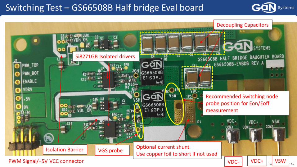
Switching Test – GS66508B Half bridge Eval board
PWM Signal/+5V VCC connector
Si8271GB Isolated drivers
Decoupling Capacitors
VDC- VDC+ VSW
Optional current shuntUse copper foil to short if not used
Isolation Barrier
Recommended Switching node probe position for Eon/Eoffmeasurement
VGS probe

GaN Systems – 41
GS66508B-EVBDB PCB Layout
Top Layer Mid layer 1
Mid layer 2 Bottom Layer
VDC+
GND
GND
VSWVSW
GND
VSW
GND
0V_GDH
0V_GDL
VSW
GND
GND

GaN Systems – 42
Double pulse switching test
VDS 400V
VGS
Inductor current IL30A
VDS=400V, ID=30A, RGON=10Ω, RGOFF=1 Ω
Q1
Q2
LOUT
400V DC
+
VDC+
VSWVDS
VGL
IL
GS66508B hard switched up to 400V/30A

GaN Systems – 43
GS66508 Double pulse switching test
VDS = 400V
IL = 30A
VDS=400V, ID=30A Hard Switching Turn-on
VGS
VDS dip due to loop inductance:∆V=Lp*di/dt
Peak turn-on dv/dt=80V/ns
VDS=400V, ID=30A Hard Switching Turn-off
IL = 30A
Peak Turn-off dv/dt>100V/nstr = 3.9ns
VDS peak = 450V
Clean rising edge w/ low Vdsovershoot (low loop inductance)
Estimated Loop inductance = 3nH
Clean VGS waveforms

GaN Systems – 44
Summary
This application guide summarized the key design considerations for GaN Systems GaN E-HEMTs. We started with the fundamental aspects of GaN E-HEMTs and then the gate drive design considerations were discussed. A list of recommended drivers and several gate drive reference designs were provided.
The second part of this guide focused on the PCB layout and discussed the layout best practice by using GaN Systems Embedded package GaNPx.
At last a real half bridge evaluation board design following the design recommendations in this document was built and its switching performance was tested.
The switching test results showed fast and clean hard switching waveforms up to full rated current 400V/30A with minimum ringing/overshoot. This concluded that with optimum gate drive and board layout combined with low GaNPx inductance, GaN E-HEMTs exhibit optimum switching performance

GaN Systems – 45
Design resources
Datasheets, spice models: http://www.gansystems.com/transistors.php
Evaluation boards: http://www.gansystems.com/eval-boards.php
Application notes: http://www.gansystems.com/whitepapers.php
PCB Footprint libraries: http://gansystems.com/design_library_files.php
FAQ: http://www.gansystems.com/faq-e-mode-hemts.php

GaN Systems – 46
www.gansystems.com • North America • Europe • Asia
Tomorrow’s power todayTM