GModel SNB-11827; No.of Pages14 ARTICLE IN PRESS Sensors ...home.eps.hw.ac.uk/~ryf1/Sens. Actuat B...
14
Please cite this article in press as: Y.Q. Fu, et al., Recent developments on ZnO films for acoustic wave based bio-sensing and microfluidic applications: a review, Sens. Actuators B: Chem. (2009), doi:10.1016/j.snb.2009.10.010 ARTICLE IN PRESS G Model SNB-11827; No. of Pages 14 Sensors and Actuators B xxx (2009) xxx–xxx Contents lists available at ScienceDirect Sensors and Actuators B: Chemical journal homepage: www.elsevier.com/locate/snb Recent developments on ZnO films for acoustic wave based bio-sensing and microfluidic applications: a review Y.Q. Fu a,b,∗ , J.K. Luo b,c , X.Y. Du b , A.J. Flewitt b , Y. Li d , G.H. Markx a , A.J. Walton d , W.I. Milne b a School of Engineering and Physical Sciences, Heriot Watt University, Edinburgh, EH14 4AS, UK b Department of Engineering, University of Cambridge, JJ Thomson Avenue, CB3 0FA, UK c Centre for Material Research and Innovation, University of Bolton, Deane Road, Bolton, BL3 5AB, UK d Scottish Microelectronics Centre, School of Engineering, University of Edinburgh, Edinburgh, EH10 7AT, UK article info Article history: Received 8 June 2009 Received in revised form 8 September 2009 Accepted 2 October 2009 Available online xxx Keywords: ZnO Film Biosensor Microfluidics SAW FBAR Lab on chip abstract Recent developments on the preparation and application of ZnO films for acoustic wave-based microflu- idics and biosensors are reviewed in this paper. High quality and strongly textured ZnO thin films can be prepared using many technologies, among which RF magnetron sputtering is most commonly used. This paper reviews the deposition of ZnO film and summarizes the factors influencing the microstructure, texture and piezoelectric properties of deposited ZnO films. ZnO acoustic wave devices can be success- fully used as biosensors, based on the biomolecule recognition using highly sensitive shear horizontal and Love-wave surface acoustic waves, as well as film bulk acoustic resonator devices. The acoustic wave generated on the ZnO acoustic devices can induce significant acoustic streaming, small scale fluid mixing, pumping, ejection and atomization, depending on the wave mode, amplitude and surface condition. The potential to fabricate an integrated lab-on-a-chip diagnostic system based on these ZnO acoustic wave technologies is also discussed. © 2009 Elsevier B.V. All rights reserved. 1. Introduction Acoustic wave technology and devices have been in commer- cial use (such as communications, automotive and environmental sensing) for more than 60 years [1,2]. When an alternating electric field is applied to an interdigital transducer (IDT) on a piezoelectric material, a mechanical wave can be generated and propagates into the material perpendicular to the surface into the bulk (bulk acous- tic wave, BAW) or on the surface of the material (surface acoustic wave, SAW) through a piezoelectric effect, either in a Rayleigh mode (vertical and surface normal) or as a shear wave (horizon- tal in-plane) [3]. Table 1 lists some common acoustic wave modes and related sensors. The most commonly used bulk acoustic wave device is the quartz crystal microbalance (QCM), which is gener- ally made of quartz sandwiched between two electrodes. A surface acoustic wave propagating within a thin surface layer, which has a lower acoustic velocity than that of the piezoelectric substrate, is called a Love wave. Love-wave devices are typically operated in the shear horizontal (SH) wave mode. A wave propagating in a thin plate with a thickness much less than the acoustic wave- ∗ Corresponding author at: School of Engineering and Physical Sciences, Heriot Watt University, Edinburgh, EH14 4AS, UK. E-mail address: [email protected] (Y.Q. Fu). length is called a flexural plate wave or Lamb wave [4]. This paper first highlights acoustic wave-based microfluidics and biosensor technology before discussing the ZnO based ones. The following section reviews the deposition of ZnO film and summarizes the factors influencing the microstructure, texture and piezoelectric properties of deposited ZnO films. Bio-sensing and microfluidics applications based on the ZnO acoustic wave devices are reviewed. The potential to fabricate an integrated lab-on-a-chip diagnostic system based on these ZnO acoustic wave technologies is also dis- cussed. 2. Acoustic wave bio-sensors and microfluidics 2.1. Acoustic wave biosensors Most acoustic wave devices can be used as sensors because they are sensitive to mechanical, chemical, or electrical perturbations on the surface of the device [5,6]. Acoustic wave sensors have the advantage that they are versatile, sensitive, and reliable. They can detect not only mass/density changes, but also viscosity, wave func- tions, elastic modulus, conductivity and dielectric properties and have wide applications in monitoring of pressure, moisture, tem- perature, force, acceleration, shock, viscosity, flow, pH levels, ionic contaminants, odour, radiation and electric fields [7,8]. Recently, 0925-4005/$ – see front matter © 2009 Elsevier B.V. All rights reserved. doi:10.1016/j.snb.2009.10.010
Transcript of GModel SNB-11827; No.of Pages14 ARTICLE IN PRESS Sensors ...home.eps.hw.ac.uk/~ryf1/Sens. Actuat B...

G
S
Rm
Ya
b
c
d
a
ARRAA
KZFBMSFL
1
csfimttwmtadaaaiia
W
0d
ARTICLE IN PRESSModel
NB-11827; No. of Pages 14
Sensors and Actuators B xxx (2009) xxx–xxx
Contents lists available at ScienceDirect
Sensors and Actuators B: Chemical
journa l homepage: www.e lsev ier .com/ locate /snb
ecent developments on ZnO films for acoustic wave based bio-sensing andicrofluidic applications: a review
.Q. Fua,b,∗, J.K. Luob,c, X.Y. Dub, A.J. Flewittb, Y. Lid, G.H. Markxa, A.J. Waltond, W.I. Milneb
School of Engineering and Physical Sciences, Heriot Watt University, Edinburgh, EH14 4AS, UKDepartment of Engineering, University of Cambridge, JJ Thomson Avenue, CB3 0FA, UKCentre for Material Research and Innovation, University of Bolton, Deane Road, Bolton, BL3 5AB, UKScottish Microelectronics Centre, School of Engineering, University of Edinburgh, Edinburgh, EH10 7AT, UK
r t i c l e i n f o
rticle history:eceived 8 June 2009eceived in revised form 8 September 2009ccepted 2 October 2009vailable online xxx
a b s t r a c t
Recent developments on the preparation and application of ZnO films for acoustic wave-based microflu-idics and biosensors are reviewed in this paper. High quality and strongly textured ZnO thin films can beprepared using many technologies, among which RF magnetron sputtering is most commonly used. Thispaper reviews the deposition of ZnO film and summarizes the factors influencing the microstructure,texture and piezoelectric properties of deposited ZnO films. ZnO acoustic wave devices can be success-fully used as biosensors, based on the biomolecule recognition using highly sensitive shear horizontal
eywords:nOilmiosensoricrofluidics
AW
and Love-wave surface acoustic waves, as well as film bulk acoustic resonator devices. The acoustic wavegenerated on the ZnO acoustic devices can induce significant acoustic streaming, small scale fluid mixing,pumping, ejection and atomization, depending on the wave mode, amplitude and surface condition. Thepotential to fabricate an integrated lab-on-a-chip diagnostic system based on these ZnO acoustic wavetechnologies is also discussed.
BARab on chip
. Introduction
Acoustic wave technology and devices have been in commer-ial use (such as communications, automotive and environmentalensing) for more than 60 years [1,2]. When an alternating electriceld is applied to an interdigital transducer (IDT) on a piezoelectricaterial, a mechanical wave can be generated and propagates into
he material perpendicular to the surface into the bulk (bulk acous-ic wave, BAW) or on the surface of the material (surface acousticave, SAW) through a piezoelectric effect, either in a Rayleighode (vertical and surface normal) or as a shear wave (horizon-
al in-plane) [3]. Table 1 lists some common acoustic wave modesnd related sensors. The most commonly used bulk acoustic waveevice is the quartz crystal microbalance (QCM), which is gener-lly made of quartz sandwiched between two electrodes. A surfacecoustic wave propagating within a thin surface layer, which has
Please cite this article in press as: Y.Q. Fu, et al., Recent developments oapplications: a review, Sens. Actuators B: Chem. (2009), doi:10.1016/j.snb.
lower acoustic velocity than that of the piezoelectric substrate,s called a Love wave. Love-wave devices are typically operatedn the shear horizontal (SH) wave mode. A wave propagating in
thin plate with a thickness much less than the acoustic wave-
∗ Corresponding author at: School of Engineering and Physical Sciences, Heriotatt University, Edinburgh, EH14 4AS, UK.
E-mail address: [email protected] (Y.Q. Fu).
925-4005/$ – see front matter © 2009 Elsevier B.V. All rights reserved.oi:10.1016/j.snb.2009.10.010
© 2009 Elsevier B.V. All rights reserved.
length is called a flexural plate wave or Lamb wave [4]. This paperfirst highlights acoustic wave-based microfluidics and biosensortechnology before discussing the ZnO based ones. The followingsection reviews the deposition of ZnO film and summarizes thefactors influencing the microstructure, texture and piezoelectricproperties of deposited ZnO films. Bio-sensing and microfluidicsapplications based on the ZnO acoustic wave devices are reviewed.The potential to fabricate an integrated lab-on-a-chip diagnosticsystem based on these ZnO acoustic wave technologies is also dis-cussed.
2. Acoustic wave bio-sensors and microfluidics
2.1. Acoustic wave biosensors
Most acoustic wave devices can be used as sensors because theyare sensitive to mechanical, chemical, or electrical perturbationson the surface of the device [5,6]. Acoustic wave sensors have theadvantage that they are versatile, sensitive, and reliable. They can
n ZnO films for acoustic wave based bio-sensing and microfluidic2009.10.010
detect not only mass/density changes, but also viscosity, wave func-tions, elastic modulus, conductivity and dielectric properties andhave wide applications in monitoring of pressure, moisture, tem-perature, force, acceleration, shock, viscosity, flow, pH levels, ioniccontaminants, odour, radiation and electric fields [7,8]. Recently,
ARTICLE IN PRESSG Model
SNB-11827; No. of Pages 14
2 Y.Q. Fu et al. / Sensors and Actuators B xxx (2009) xxx–xxx
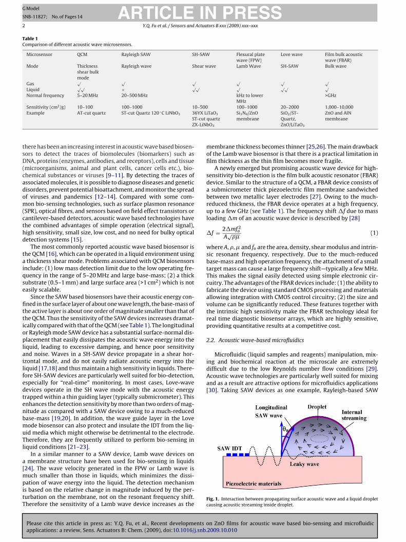
Table 1Comparison of different acoustic wave microsensors.
Microsensor QCM Rayleigh SAW SH-SAW Flexural platewave (FPW)
Love wave Film bulk acousticwave (FBAR)
Mode Thicknessshear bulkmode
Rayleigh wave Shear wave Lamb Wave SH-SAW Bulk wave
Gas√ √ √ √ √ √
Liquid√√ × √√ √ √√ √
Normal frequency 5–20 MHz 20–500 MHz kHz to lowerMHz
>GHz
Sensitivity (cm2/g) 10–100 100–1000 10–500 100–1000 20–2000 1,000–10,0006YX LT-cutX-LiN
tsD(cadom(cthd
taiqse
fittioplailfedtenbmuTl
a[mpitT
ing and biochemical reaction at the microscale are extremelydifficult due to the low Reynolds number flow conditions [29].Acoustic wave technologies are particularly well suited for mixingand as a result are attractive options for microfluidics applications[30]. Taking SAW devices as one example, Rayleigh-based SAW
Example AT-cut quartz ST-cut Quartz 120 ◦C LiNbO3 3SZ
here has been an increasing interest in acoustic wave based biosen-ors to detect the traces of biomolecules (biomarkers) such asNA, proteins (enzymes, antibodies, and receptors), cells and tissue
microorganisms, animal and plant cells, cancer cells etc.), bio-hemical substances or viruses [9–11]. By detecting the traces ofssociated molecules, it is possible to diagnose diseases and geneticisorders, prevent potential bioattachment, and monitor the spreadf viruses and pandemics [12–14]. Compared with some com-on bio-sensing technologies, such as surface plasmon resonance
SPR), optical fibres, and sensors based on field effect transistors orantilever-based detectors, acoustic wave based technologies havehe combined advantages of simple operation (electrical signal),igh sensitivity, small size, low cost, and no need for bulky opticaletection systems [15].
The most commonly reported acoustic wave based biosensor ishe QCM [16], which can be operated in a liquid environment usingthickness shear mode. Problems associated with QCM biosensors
nclude: (1) low mass detection limit due to the low operating fre-uency in the range of 5–20 MHz and large base-mass; (2) a thickubstrate (0.5–1 mm) and large surface area (>1 cm2) which is notasily scalable.
Since the SAW based biosensors have their acoustic energy con-ned in the surface layer of about one wave length, the base-mass ofhe active layer is about one order of magnitude smaller than that ofhe QCM. Thus the sensitivity of the SAW devices increases dramat-cally compared with that of the QCM (see Table 1). The longitudinalr Rayleigh mode SAW device has a substantial surface-normal dis-lacement that easily dissipates the acoustic wave energy into the
iquid, leading to excessive damping, and hence poor sensitivitynd noise. Waves in a SH-SAW device propagate in a shear hor-zontal mode, and do not easily radiate acoustic energy into theiquid [17,18] and thus maintain a high sensitivity in liquids. There-ore SH-SAW devices are particularly well suited for bio-detection,specially for “real-time” monitoring. In most cases, Love-waveevices operate in the SH wave mode with the acoustic energyrapped within a thin guiding layer (typically submicrometer). Thisnhances the detection sensitivity by more than two orders of mag-itude as compared with a SAW device owing to a much-reducedase-mass [19,20]. In addition, the wave guide layer in the Loveode biosensor can also protect and insulate the IDT from the liq-
id media which might otherwise be detrimental to the electrode.herefore, they are frequently utilized to perform bio-sensing iniquid conditions [21–23].
In a similar manner to a SAW device, Lamb wave devices onmembrane structure have been used for bio-sensing in liquids
24]. The wave velocity generated in the FPW or Lamb wave is
Please cite this article in press as: Y.Q. Fu, et al., Recent developments oapplications: a review, Sens. Actuators B: Chem. (2009), doi:10.1016/j.snb.
uch smaller than those in liquids, which minimizes the dissi-ation of wave energy into the liquid. The detection mechanism
s based on the relative change in magnitude induced by the per-urbation on the membrane, not on the resonant frequency shift.herefore the sensitivity of a Lamb wave device increases as the
iTaO3
quartzbO3
Si3N4/ZnOmembrane
SiO2/ST-Quartz,ZnO/LiTaO3
ZnO and AlNmembrane
membrane thickness becomes thinner [25,26]. The main drawbackof the Lamb wave biosensor is that there is a practical limitation infilm thickness as the thin film becomes more fragile.
A newly emerged but promising acoustic wave device for high-sensitivity bio-detection is the film bulk acoustic resonator (FBAR)device. Similar to the structure of a QCM, a FBAR device consists ofa submicrometer thick piezoelectric film membrane sandwichedbetween two metallic layer electrodes [27]. Owing to the much-reduced thickness, the FBAR device operates at a high frequency,up to a few GHz (see Table 1). The frequency shift �f due to massloading �m of an acoustic wave device is described by [28]
�f = 2�mf 2o
A√
��(1)
where A, �, � and fo are the area, density, shear modulus and intrin-sic resonant frequency, respectively. Due to the much-reducedbase-mass and high operation frequency, the attachment of a smalltarget mass can cause a large frequency shift—typically a few MHz.This makes the signal easily detected using simple electronic cir-cuitry. The advantages of the FBAR devices include: (1) the ability tofabricate the device using standard CMOS processing and materialsallowing integration with CMOS control circuitry; (2) the size andvolume can be significantly reduced. These features together withthe intrinsic high sensitivity make the FBAR technology ideal forreal time diagnostic biosensor arrays, which are highly sensitive,providing quantitative results at a competitive cost.
2.2. Acoustic wave-based microfluidics
Microfluidic (liquid samples and reagents) manipulation, mix-
n ZnO films for acoustic wave based bio-sensing and microfluidic2009.10.010
Fig. 1. Interaction between propagating surface acoustic wave and a liquid dropletcausing acoustic streaming inside droplet.

ARTICLE IN PRESSG Model
SNB-11827; No. of Pages 14
Y.Q. Fu et al. / Sensors and Actuators B xxx (2009) xxx–xxx 3
Table 2Comparison of common piezoelectric materials.
Materials ZnO AlN PZT Quartz 128◦ cut LiNbO3 36◦ cut LiTaO3 PVDF
Density (g/cm3) 5.61 3.3 7.8 2.64 4.64 7.45 1.79Moulus (GPa) 110–140 300–350 61 71.7 225 0.16Hardness 4–5 GPa 15 GPa 7–18 GPa Moh’s 7 Moh’s 5 Knoop 800–1000 70–110 Knoop 700–1200 Shore D75–85Refractive index 1.9–2.0 1.96 2.40 1.46 2.29 2.18 1.42Piezo-constant d33(pC/N)
12 4.5, 6.4 289–380, 117 2.3 (d11) 19–27 −21 −35
Coupling coefficient, k 0.15–0.28, 0.33 0.17–0.5 0.49 0.0014 0.23 0.2 0.12–0.2Effective couplingcoeff. k2 (%)
1.5–1.7 3.1–8 20–35 8.8–16 2–11.3 0.66–0.77 2.9
Acoustic velocity by 6336 (2650) 11,050 (6,090) 4500 (2200) 5960 (3310) 3970 3230–3295 2600
.3
.5
watWoaob
�
warmat
P
idcuruawfptpssp
2
mfotibl(ie
transverse (m/s)Dielectric constant 8.66 8.5–10 380 4Coefficient of thermalexpansion (CTE, ×10−6)
4 5.2 1.75 5
aves have a longitudinal component that can be coupled withmedium in contact with the device’s surface. This coupling can
ransport the media on the surface during its propagation [31].hen liquid (either in bulk or droplet form) exists on the surface
f a SAW device, the energy and momentum of the acoustic wavere coupled into the fluid at a Rayleigh angle, following Snell’s lawf diffraction (see Fig. 1) [32,33]. The Rayleigh angle, �, is definedy
= sin−1( vl
vS
)(2)
here vl and vs are the velocity of the longitudinal wave in solidnd liquid. The energy and the momentum of the longitudinal waveadiated into the liquid can be harnessed for liquid pumping andixing. A net pressure gradient, P, forms in the direction of the
coustic wave propagation and provides an effective force to drivehe liquid, which can be described by [34]
= �ov2s
(��
�o
)2
(3)
n which, �o is the liquid density and �� is the slight density changeue to the acoustic pressure. The generated acoustic pressure canreate significant acoustic streaming in a liquid and result in liq-id mixing, pumping, ejection and atomization [35]. This allowsapid movement of liquid and also internal agitation, which speedsp biochemical reactions, minimizes non-specific biobinding, andccelerates hybridization reactions in protein and DNA analysishich is commonly used in proteomics and genomics [36,37]. Sur-
ace acoustic wave based liquid pumps and mixers [38,39], dropletositioning and manipulation [40], droplet ejection and atomiza-ion systems [41,42], and fluidic dispenser arrays [43] have beenroposed and developed. They have distinct advantages, such asimple device structure, no moving-parts, electronic control, highpeed, programmability, manufacturability, remote control, com-actness and high frequency response [44–46].
.3. Selection of bulk materials or thin films
Acoustic wave devices can be used for both bio-sensing andicrofluidics applications, which are two of the major components
or lab-on-a-chip systems. Therefore, it is attractive to develop lab-n-chip bio-detection platforms using acoustic wave devices ashis integrates the functions of micro-droplet transportation, mix-ng and bio-detection. To date, most of the acoustic devices have
Please cite this article in press as: Y.Q. Fu, et al., Recent developments oapplications: a review, Sens. Actuators B: Chem. (2009), doi:10.1016/j.snb.
een made from bulk piezoelectric materials, such as quartz (SiO2),ithium tantalate (LiTaO3), lithium niobate (LiNbO3) and sapphireAl2O3). These bulk materials are expensive, and are less easilyntegrated with electronics for control and signal processing. Piezo-lectric thin films such as ZnO have good piezoelectric properties,
85 (29) 54 (43) 6–815 −16.5 42–75
high electro-mechanical coupling coefficient, high sensitivity andreliability [47]. They can be grown in thin film form on a vari-ety of substrates, including silicon, making them perhaps the mostpromising material for integration with electronic circuitry, aimingfor disposal, low-price and mass production [48]. This approach islikely to be the future of acoustic wave based lab-on-a-chip bio-sensing devices.
ZnO, AlN and PZT are the three dominant piezoelectric thinfilm materials which can be integrated into MEMS and microelec-tronics processes. Gallium arsenide (GaAs), silicon carbide (SiC),polyvinylidene fluoride (PVDF) and its copolymers are less commonthin film piezoelectric (PE) materials (see Table 2). Among these,PZT has the highest piezoelectric constant and electro-mechanicalcoupling coefficient. However, for biosensor applications, PZT filmshave disadvantages such as higher acoustic wave attenuation,lower sound wave velocities, and poor biocompatibility. Piezoelec-tric AlN thin films have a much higher phase velocity, and are hardand chemically stable (see Table 2). However, the deposition of AlNfilms and texture control are more difficult compared with that forZnO. Other PE films are either too expensive such as GaAs and SiCor too weak in their piezoelectric effect, e.g., PE-polymers [49,50].Compared with AlN, ZnO shows a higher piezoelectric coupling,and it is much easier to control the film stoichiometry, texture andother properties [51]. Zinc oxide is biosafe and therefore suitablefor biomedical applications to immobilize and modify biomoleculeswithout toxic effects [52]. This paper summarizes recent develop-ments in the preparation and application of ZnO films for acousticwave-based microfluidics and biosensors, and also discusses futuretrends for ZnO film based lab-on-a-chip applications.
3. Requirement for ZnO film for sensing and microfluidicapplications
For the successful application of ZnO films for acoustic wavebio-sensing and microfluidic applications, there are some basicrequirements which include:
(1) Microstructure issues:• Strong texture.• High crystal quality and low defects.• Uniformity in film microstructure and thickness.• Smooth surface and low roughness.• Good stoichiometry (Zn/O ratio).
n ZnO films for acoustic wave based bio-sensing and microfluidic2009.10.010
(2) Good piezoelectric properties:• High frequency and large acoustic velocity.• High electro-mechanical coupling coefficient k2.• Low acoustic loss.• High quality factor Q.

IN PRESSG
S
4 Actuators B xxx (2009) xxx–xxx
(
(
Ti
4
4
tdmapfscso
Zpaistmsamtr
(
TA
ARTICLEModel
NB-11827; No. of Pages 14
Y.Q. Fu et al. / Sensors and
• Good thermal or temperature stability (low thermal coeffi-cient of frequency or velocity).
3) Fabrication requirement:• Compatible with MEMS or CMOS technology.• Easy deposition on different substrates and complex shape.• High deposition rate.• Low cost and mass production.• Reproducibility/high yield.• Low film stress/good adhesion to substrates.
4) Microfluidics and biosensor:• High sensitivity and selectivity.• Stability of performance.• High pumping/mixing efficiency.• Easy functionalization of surfaces for immobilization of anti-
bodies.• Biocompatibility.
he following sections focus on recent progress covering the abovessues.
. ZnO film and piezoelectric properties
.1. Deposition and microstructure
Many different methods have been reported for the deposi-ion of ZnO films, including sol–gel processes, chemical vapoureposition, metal-organic chemical vapour deposition, sputtering,olecular beam epitaxy, pulsed laser deposition, filtered vacuum
rc deposition and atomic layer deposition [53–56]. Table 3 com-ares different deposition methods for the ZnO films. From a MEMSabrication point of view, radio-frequency (RF) magnetron reactiveputtering is one of the best methods, with good reproducibility andompatibility with planar device fabrication technology [57]. In thisection, we will focus on the texture and acoustic wave propertiesf sputtered ZnO films.
The microstructure, texture and piezoelectric properties of thenO films are normally affected by sputtering conditions such aslasma power, gas pressure, and substrate material and temper-ture as well as film thickness. During sputtering, the energeticon bombardment has significant effects on the stoichiometry, size,hape and orientation of ZnO crystals, intrinsic stress, defects, elec-rical and optical properties, as well as surface and cross-section
orphologies. The effects of the processing parameters, such asputtering gas pressure, RF power, total flux density, bias voltagend substrate temperature, have been successfully described usingodified Thornton models [58,59]. Some general conclusions about
he effects of sputtering parameters on ZnO thin films are summa-ized as follows:
Please cite this article in press as: Y.Q. Fu, et al., Recent developments oapplications: a review, Sens. Actuators B: Chem. (2009), doi:10.1016/j.snb.
1) Higher plasma or bias power results in a higher deposition ratebecause the deposited particles have higher kinetic energies.However, the film surface roughness could increase signifi-cantly at a higher power, due to the ion bombardment effect.
able 3comparison of different types of deposition methods.
Sputtering CVD and MOCVD Laser ab
Epitaxialgrowth
Possible Yes Yes
Deposition rate Medium (a few nm/s) Low (0.2 to a few nm/s) Low (0.1Compatibilitywith MEMSprocessing
Good Ok Poor
Temperature 25–400 ◦C 300–900 ◦C 200–600Quality Good Good GoodCost Slightly cost Medium MediumDeposition size Large area Large area Small si
Fig. 2. ZnO crystalline structure–Wurtzite structure (modified following Ref. [1])with directions of [0 0 0 1], [1 1 −2 0] and [1 0 −1 0] indicated. The lattice constantsare a = 3.25 Å and c = 5.2 Å.
(2) Low gas pressure generally results in a dense and fine grain film.Higher gas pressure could result in porous, columnar films withrough surfaces [60].
(3) The gas ratio of O2/Ar is a critical parameter and a sufficientoxygen partial pressure is needed to maintain the stoichiometryof the ZnO films.
(4) ZnO thin films can be deposited at low temperature (<200 ◦C),which is compatible with existing CMOS circuitry on a chip.However, high temperature deposition will enhance the atommobility, decrease the defects, promote film adhesion to thesubstrate, improve film texture, quality and increase grain size,resulting in a compact and dense film structure.
(5) The sputtered film normally shows a good piezoelectric effect.Thus post-deposition poling to obtain a good piezoelectriceffect is unnecessary.
4.2. Film texture
The film texture of the ZnO film is crucial for the piezoelectricand acoustic wave properties of the acoustic devices. The sub-strate has significant influences on nucleation, growth and texture,acoustic wave velocity/frequency, and electro-mechanical couplingcoefficient of the ZnO acoustic wave devices.
4.2.1. Self-texture and wave modeZnO normally crystallizes in a hexagonal, quartzite type crys-
n ZnO films for acoustic wave based bio-sensing and microfluidic2009.10.010
talline structure [61] (see Fig. 2), which is dominated by threecrystal planes: (0 0 0 1), (101̄0) and (112̄0), with their surfaceenergy densities of 0.99, 0.123, and 0.209 eV/Å2, respectively [62].The (0 0 0 1) plane has the lowest surface free energy. There-fore, under equilibrium, if there is no epitaxy between the film
lation MBE Sol–gel FCVA
Highly Difficult Possible
to 0.4 nm/s) Very low High High (0.2–15 nm/s)Poor Good Poor
◦C 300–800 ◦C Room temperature LowExcellent Poor GoodHigh Cheap Medium
ze Medium Large area Small size

ARTICLE IN PRESSG Model
SNB-11827; No. of Pages 14
Y.Q. Fu et al. / Sensors and Actuators B xxx (2009) xxx–xxx 5
Table 4Summary of velocity of the ZnO films: (1) most data from SAW devices, (2) the data is only for comparison, as the velocity is related to the film thickens, thus the comparisonof velocities is no meaning unless the film thickness is the same.
Device type Substrate materials Structure Lattice difference Velocity (m/s) Temperature expansioncoefficient (10−6 K−1)
ZnO ZnO HCP 2724 2.9 (4.751)ZnO/Si Si (1 1 1) Cubic 41.3% 2653 3ZnO/Pt Pt (1 1 1) Cubic 1.8% 2684 8.8ZnO/Au Au (1 1 1) Cubic 2.5% 14ZnO/SiO2 Quartz 4200 13.2 (a)/7.1cSapphire Al2O3 (0 0 0 1) HCP 31.8% 4000–5750 7.3 (18.1)ZnO/LiNbO3 LiNbO3 (0 0 0 1) HCP 14.8 (4.1)ZnO/sapphire Sapphire (0 0 0 1) HCP 31.8% 8.4 (5.3)ZnO/GaN GaN HCP 1.8% 3.17ZnO/AlN AlN HCP 4.1% 4522 5.3 (4.1)
aectbdae
ub
Fss
ZnO/DLC DLC AmorphousNanocrystalline diamondZnO/diamond Diamond (1 1 1) CubicZnO/AlN/diamond ZnO/AlN/diamond
nd substrate, or without any external energy source, the filmsxhibit self-texture and grow along the (0 0 0 1) orientation, on bothrystalline and amorphous substrates [63]. However, as the filmhickness increases, the other orientation peaks might appear andecome stronger [64]. Excess Zn during film growth can cause theeterioration of the ZnO film crystallinity [65]. The O2/Ar gas rationd gas pressure have frequently been reported to have significant
Please cite this article in press as: Y.Q. Fu, et al., Recent developments oapplications: a review, Sens. Actuators B: Chem. (2009), doi:10.1016/j.snb.
ffects on the film stress and texture [61–65].ZnO acoustic wave devices with a (0 0 0 1) film texture can be
sed for sensing in air or gaseous environments. However, manyiosensors need to detect chemical reactions in a liquid environ-
ig. 3. SEM cross-section morphologies of ZnO films deposited using magnetronputtering method: (a) under target; (b) far away from target showing the inclinedtructure due to ion channeling effect.
5000–70008500 1.18
10,000–12,000 1.1812,200
ment. For bio-sensing in liquids, it is necessary to generate a shearhorizontal mode wave, where the wave displacement is withinthe plane of the crystal surface [66,67]. For generation of such ashear horizontal wave, other film textures such as the (112̄0) and(101̄01 0 −1 0) are necessary [68].
4.2.2. Interlayer or buffer layerAn amorphous ZnO intermediate layer is normally formed
before the growth of the crystalline ZnO layer on substrates such asNi, Cu, Si, Ti and glass, and this layer is about 10–50 nm dependingon the type of substrates [69,70]. Self-textured (0 0 0 1) ZnO filmsslowly grow on this amorphous layer, which is probably the reasonwhy the ZnO films deposited on Ni, Cu, and Cr substrates show poortexture. No such amorphous interlayer was observed on Au, Ru, Pt,Al and sapphire substrates [71,72], and the ZnO films deposited onthese substrates show good (0 0 0 1) orientation. Buffer layers arefrequently used to enhance the film crystalline quality and texture,for example, AlN, MgO, Al2O3, GaN, DLC, and SiO2 (see Table 4)[73–75] and they can also be used to promote the epitaxial growthof ZnO films.
4.2.3. Epitaxial growthEpitaxial growth on different substrates can lead to different
ZnO orientations. The growth of ZnO can be attributed to the com-petition between the lowest surface free energy (0 0 0 1) of ZnOand the closest lattice mismatch between the ZnO growth planeand the substrate plane (see Table 4) [76]. However, this is sig-nificantly dependent on the deposition methods and substratematerials. MBE, pulsed laser deposition, MOCVD and sputter-ing have been frequently been used to grow the ZnO epitaxialfilms [77,78]. The common substrates for epitaxial growth of theZnO film include: quartz, sapphire, LiNbO3, SrTiO3, diamond, andMgO.
4.2.4. Oxygen ion bombardmentDuring ZnO sputtering, a directional oxygen ion beam, at an
angle towards the substrate surface, plays an important role inchanging the ZnO film texture from a (0 0 0 1) texture into (101̄0)or (112̄0) texture due to ion channeling effect [79]. The ZnO filmswith these two textures can excite a shear acoustic wave withouta longitudinal wave [80]. A pre-requisite for the significant oxygenion bombardment effect is a low gas pressure which contributes to
n ZnO films for acoustic wave based bio-sensing and microfluidic2009.10.010
a longer mean free path for the oxygen ion bombarding the film sur-face. ZnO films at different positions on the substrate under plasmaalso show different crystal orientations (see Fig. 3) [81], which caneasily be explained by the oxygen ion bombardment angle effectsunder the target.
IN PRESSG
S
6 Actuators B xxx (2009) xxx–xxx
tt
(
((
(
(
(
4
4
ssvva2fataa
4
n
4S
(
(
(
ARTICLEModel
NB-11827; No. of Pages 14
Y.Q. Fu et al. / Sensors and
In summary, a (0 0 0 1) film texture is commonly observed forhe sputtered ZnO films. In order to obtain the other types of filmexture, the following methods could be used:
1) Epitaxial growth on a specific substrate using a suitable depo-sition method;
2) controling the sample position under the plasma [82];3) using an additional anode near the substrate, which can have
an apparent orientating effect on the growing films [83];4) substrate tilting with a set angle due to the oblique incidence
of the particles on the growing film;5) using an external oxygen ion source and control the oxygen ion
bombardment during film growth;6) using a blind which can be positioned between the target and
substrate to only allow oblique particles to be incident on sub-strate surface [84].
.3. Piezoelectric properties of sputtered ZnO films
.3.1. Substrate effectThe acoustic velocity of a ZnO film significantly depends on the
ubstrate on which it is grown. The ZnO film deposited on a sub-trate with large acoustic velocity will exhibit an increased velocityalue. Therefore, by selecting a substrate with a large acousticelocity, the wave velocity in the ZnO SAW devices can be increasedccordingly. For example, the acoustic velocity of bulk ZnO is724 m/s; it becomes 4522 m/s for ZnO/AlN; and up to 12,200 m/sor a ZnO/AlN/diamond substrate [85,86]. Table 4 summarizes thecoustic velocities of the ZnO films on different substrates. Amonghem, AlN, DLC, nano-diamond films and diamond are regardeds the best substrate materials to provide a dramatic increase incoustic wave velocities in the ZnO films [87–89].
.3.2. Film thickness effectAcoustic velocity depends significantly on the ZnO film thick-
ess for both the ZnO based SAW and FBAR devices.
.3.2.1. ZnO SAW devices. The ZnO film thickness effect for a ZnO/SiAW devices can be summarized as follows [90,91]:
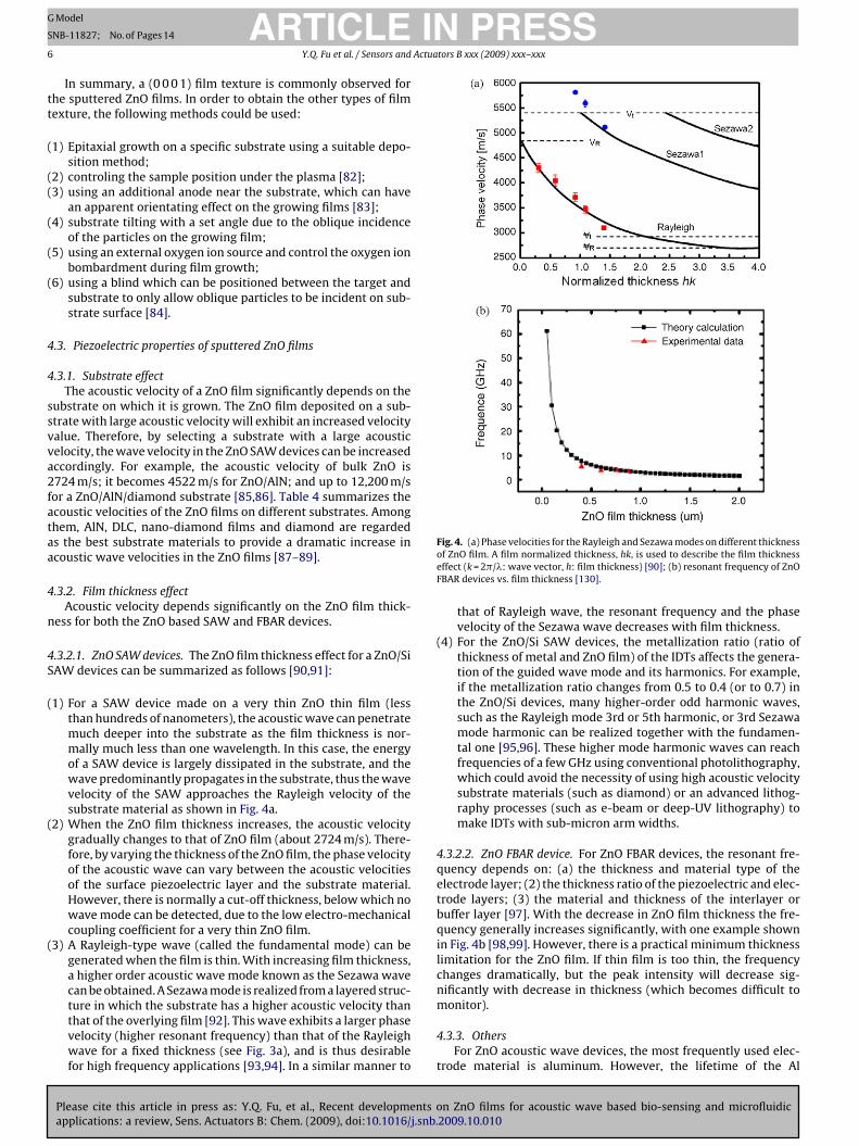
1) For a SAW device made on a very thin ZnO thin film (lessthan hundreds of nanometers), the acoustic wave can penetratemuch deeper into the substrate as the film thickness is nor-mally much less than one wavelength. In this case, the energyof a SAW device is largely dissipated in the substrate, and thewave predominantly propagates in the substrate, thus the wavevelocity of the SAW approaches the Rayleigh velocity of thesubstrate material as shown in Fig. 4a.
2) When the ZnO film thickness increases, the acoustic velocitygradually changes to that of ZnO film (about 2724 m/s). There-fore, by varying the thickness of the ZnO film, the phase velocityof the acoustic wave can vary between the acoustic velocitiesof the surface piezoelectric layer and the substrate material.However, there is normally a cut-off thickness, below which nowave mode can be detected, due to the low electro-mechanicalcoupling coefficient for a very thin ZnO film.
3) A Rayleigh-type wave (called the fundamental mode) can begenerated when the film is thin. With increasing film thickness,a higher order acoustic wave mode known as the Sezawa wavecan be obtained. A Sezawa mode is realized from a layered struc-
Please cite this article in press as: Y.Q. Fu, et al., Recent developments oapplications: a review, Sens. Actuators B: Chem. (2009), doi:10.1016/j.snb.
ture in which the substrate has a higher acoustic velocity thanthat of the overlying film [92]. This wave exhibits a larger phasevelocity (higher resonant frequency) than that of the Rayleighwave for a fixed thickness (see Fig. 3a), and is thus desirablefor high frequency applications [93,94]. In a similar manner to
Fig. 4. (a) Phase velocities for the Rayleigh and Sezawa modes on different thicknessof ZnO film. A film normalized thickness, hk, is used to describe the film thicknesseffect (k = 2�/�: wave vector, h: film thickness) [90]; (b) resonant frequency of ZnOFBAR devices vs. film thickness [130].
that of Rayleigh wave, the resonant frequency and the phasevelocity of the Sezawa wave decreases with film thickness.
(4) For the ZnO/Si SAW devices, the metallization ratio (ratio ofthickness of metal and ZnO film) of the IDTs affects the genera-tion of the guided wave mode and its harmonics. For example,if the metallization ratio changes from 0.5 to 0.4 (or to 0.7) inthe ZnO/Si devices, many higher-order odd harmonic waves,such as the Rayleigh mode 3rd or 5th harmonic, or 3rd Sezawamode harmonic can be realized together with the fundamen-tal one [95,96]. These higher mode harmonic waves can reachfrequencies of a few GHz using conventional photolithography,which could avoid the necessity of using high acoustic velocitysubstrate materials (such as diamond) or an advanced lithog-raphy processes (such as e-beam or deep-UV lithography) tomake IDTs with sub-micron arm widths.
4.3.2.2. ZnO FBAR device. For ZnO FBAR devices, the resonant fre-quency depends on: (a) the thickness and material type of theelectrode layer; (2) the thickness ratio of the piezoelectric and elec-trode layers; (3) the material and thickness of the interlayer orbuffer layer [97]. With the decrease in ZnO film thickness the fre-quency generally increases significantly, with one example shownin Fig. 4b [98,99]. However, there is a practical minimum thicknesslimitation for the ZnO film. If thin film is too thin, the frequencychanges dramatically, but the peak intensity will decrease sig-nificantly with decrease in thickness (which becomes difficult to
n ZnO films for acoustic wave based bio-sensing and microfluidic2009.10.010
monitor).
4.3.3. OthersFor ZnO acoustic wave devices, the most frequently used elec-
trode material is aluminum. However, the lifetime of the Al

ING
S
Actua
eePtpitapatmTfiiS
5
soawZsoiiip
ibadlfTH
gtuhgtpttHoa
afocafil(la
i
ARTICLEModel
NB-11827; No. of Pages 14
Y.Q. Fu et al. / Sensors and
lectrode in aqueous media is limited due to significant corrosionffects. The other common electrode materials include Au, Ni, W,t, Ta and Cu. The electro-mechanical coupling coefficient (k2) ofhe ZnO/Si acoustic wave devices depends on [100,101]: (1) waveropagation mode (fundamentals or their harmonics); (2) normal-
zed thickness of ZnO film; (3) film texture; (4) film thickness; (5)he nature and dimension of the electrodes; (6) substrate materi-ls. The temperature coefficient of frequency (TCF) is an importantarameter for ZnO FBAR and SAW applications for biosensors. Therere different strategies to minimize the TCF or compensate for theemperature effect associated with ZnO based devices. The com-
on strategy is to combine a material with a positive (or negative)CF values, with another one with a negative (or positive) TCF. ZnOlm has a negative TCF value, thus an easy way to reduce the TCF
s to use a substrate or interlayer with a positive TCF value, such asiO2 or quartz [102].
. MEMS processing of ZnO films
ZnO films normally have excellent bonding to a range of sub-trate materials. However, caution is required for MEMS processingf ZnO films as they are quite reactive and sensitive to temperature,cids as well as water [103]. In fact ZnO will dissolve in deionizedater with a solubility of about 2 mg/l [104]. Hence, any rinsing of
nO films using DI water should be made in as short a time as pos-ible. Acetone can be used for cleaning the samples, but Pirana, orther strong cleaning solution should be avoided. In addition ZnOs easily hydrolyzed upon exposure to air. For MEMS processing,t is necessary to pre-bake the film and remove the moisture, thusmproving the adhesion of photoresist. However, high temperatureost-baking or annealing above 400 ◦C should be avoided.
Photoresist adheres well to clean and dry ZnO films. Themprovement of photoresist adhesion can be improved by (1) pre-aking; (2) coating with other materials, such as SiO2; (3) usingn adhesion promoter. ZnO is soluble in most acids. Althoughifferent types of etchants, such as HCl, H3PO4, HF, HNO3, alka-
ies, ammonium chloride and NH4Cl + NH4OH + H2O can be usedor removing ZnO, the etch profile is typically difficult to control.he recommended ZnO film etching solutions include [105]: (1)3PO4 + HAc + H2O (1:1:50); (2) FeCl3 + 6H2O.
ZnO can be etched using most plasma gases, including oxy-en plasma. For dry etching of ZnO films with a photoresist mask,here are two types of gas systems which have been frequentlysed [106]: (a) hydrogen based gases such as CH4/H2/Ar which canelp in obtaining an anisotropic etch profile; (b) chlorine basedases, such as Cl2/Ar, BCl3/Ar and BCl3/Cl2/Ar plasma which areoxic. Recently, a new plasma etching method using a remote Ar/H2lasma has been developed, in which the hydrogen ions contributeo efficient and fast etching [107]. Inductively coupled plasma reac-ive ion etching has also used to anisotropically etch ZnO films usingBr/Ar plasma with photoresist as the etch mask [108]. The etchingf ZnO films in the HBr/Ar gas mixture is controlled by chemicallyssisted sputter etching.
As regards microfluidic applications, ZnO is hydrophilic withcontact angle typically of 50–80◦, which is dependent on sur-
ace conditions and light exposure [109]. Ultraviolet irradiationf ZnO film results in a superhydrophilic surface [110]. For effi-ient droplet pumping, a hydrophobic surface is normally needednd methods for improving the hydrophobic properties of the ZnOlms include [111–113]: (1) spin coating PTFE (Teflon); (2) a mono-
ayer of octadecyl thiol (ODT); (3) a monolayer of octadecylesilane
Please cite this article in press as: Y.Q. Fu, et al., Recent developments oapplications: a review, Sens. Actuators B: Chem. (2009), doi:10.1016/j.snb.
ODS); (4) an octadecyltrichlorosilane (OTS) self-assembled mono-ayer (SAM). After such treatment, the contact angle can be as highs 100–120◦.
A critical issue in developing a high performance biosensors to find a simple and reliable process for functionaliza-
PRESStors B xxx (2009) xxx–xxx 7
tion of the ZnO surface through a covalent method to forma robust immobilization of appropriate probe molecules. Nor-mally Au is pre-deposited on the ZnO surface, and a cystaminesurface atomic monolayer (SAM) is formed on the Au sur-face to which antibodies will attach. Currently little work hasbeen performed on the direct surface functionalization of theZnO films. Initial studies for immobilization of antibodies onthe ZnO film surface have been realized using [114,115] (1)amine-terminated silane, 3-aminopropltryiethoxysilane, and glu-taraldehyde as the secondary crosslinker to bind a protein;(2) 3-mercaptopropyltrimethoxysilane in dry toluene; or (3)trimethoxysilane in dry toluene to immobilize the antibody. As Auis not recognised as a good CMOS compatible material, the directimmobilization on the ZnO film has its advantages for bio-sensingapplications.
6. ZnO acoustic devices for biosensor and microfluidics
6.1. Biosensor applications
6.1.1. ZnO SAW biosensorA ZnO/Si SAW device has been successfully used in the detec-
tion of PSA antibody-antigen immuno-reaction as a function of PSAconcentrations [116]. The resonance frequencies of the ZnO SAWdevices were found to shift to lower frequencies as the PSAs arespecifically immobilized on the surface-modified ZnO SAW device.A linear dependence was found between the resonance frequencychange and the PSA/ACT complex concentrations over the broaddynamic range of 2–10,000 ng/ml [140]. However, as discussedbefore, a big challenge for SAW biosensors is how to realize detec-tion in a liquid environment. SH or Love mode SAW devices arepromising technologies for biosensors used in liquid environmentsbecause of their high sensitivity and low energy dissipation. Theessential condition for a Love-wave mode is that the shear wavevelocity in the surface wave guide layer is smaller than that in thepiezoelectric substrate. For example, ZnO has a shear wave veloc-ity of 2578 m/s, whereas those of ST-cut-quartz and SiO2 are 4996and 3765 m/s, respectively. Therefore, it is reasonable to use ZnOas a guiding layer on substrates of ST-cut quartz to form Love modebiosensors. The other potential substrate materials for Love-modeZnO sensors include LiTaO3, LiNbO3 and sapphire. A ZnO Love modedevice of ZnO/90◦ rotated ST-cut quartz has a maximum sensitivityup to −18.77 × 10⁻⁸ m2 s kg−1, which is much higher than that of aSiO2/quartz Love mode SAW device [117–119].
Most of the above mentioned ZnO Love mode sensors are basedon a bulk piezoelectric substrate (for example, quartz, LiNbO3 andLiTaO3), which are expensive and incompatible with IC fabrication.In reference [120], ZnO/SiO2/Si SAW Love mode sensors were stud-ied, and the sensitivity of the devices as high as 8.64 �m2/mg (withan acoustic wave velocity of 4814.4 m/s) were reported, which isabout 2–5 times that of ZnO/LiTaO3 [121] and SiO2/quartz Love sen-sors [122]. Another promising approach for making a ZnO basedLove mode sensor is to use a polymer film (such as PMMA, poly-imide, SU-8 or parylene C) on top of the ZnO layer as the guidinglayer. This polymer waveguide layer structure however, has a rel-atively larger intrinsic attenuation than those of solid waveguidelayers.
6.1.2. ZnO Lamb biosensorIn Lamb wave sensors, the wave propagation velocity in the
membrane is slower than the acoustic wave velocity in the flu-
n ZnO films for acoustic wave based bio-sensing and microfluidic2009.10.010
ids on the surface, thus the energy is not easily dissipated and canbe used in liquid samples [123]. A ZnO based Lamb wave devicehas been used to monitor the growth of bacterium “Pseudomonasputida” in a boulus of toluene, as well as the reaction of antibodiesin an immunoassay for an antigen present in breast cancer patients

ARTICLE IN PRESSG Model
SNB-11827; No. of Pages 14
8 Y.Q. Fu et al. / Sensors and Actuators B xxx (2009) xxx–xxx
F ices; (t
[ftfbio
ig. 5. (a) Interaction between SAW and a liquid droplet on a ZnO based SAW devhe droplet on the ZnO surface.
124]. A Si/SiO2/Si3N4/Cr/Au/ZnO Lamb wave device has been usedor detecting human IgE based on conventional cystamine SAMechnology, with a sensitivity as high as 8.52 × 107 cm2/g at a wave
Please cite this article in press as: Y.Q. Fu, et al., Recent developments oapplications: a review, Sens. Actuators B: Chem. (2009), doi:10.1016/j.snb.
requency of 9 MHz [125]. In recent years, however, the Lamb waveiosensor has not been widely studied because of: (1) low sensitiv-
ty due to the low operation frequency; (2) difficulties in fabricationf thin and fragile membrane structures.
Fig. 6. A 2 �l water droplet in (a) and its movement along with the propagating
b) top view; (c) cross-section view; (d) front view of the internal streaming inside
6.1.3. ZnO FBAR biosensorFBAR biosensors have recently attracted great attention due to
their inherent advantages compared with SAW and QCM biosen-
n ZnO films for acoustic wave based bio-sensing and microfluidic2009.10.010
sors: high sensitivity, low insertion loss, high power handlingcapability and small size [126,127]. High frequency ZnO FBAR sen-sors have good sensitivity and high energy densities owing to thetrapping of the standing wave between the two electrodes, allow-
acoustic wave in (b) showing the droplet is pushing upward and forward.

ARTICLE IN PRESSG Model
SNB-11827; No. of Pages 14
Y.Q. Fu et al. / Sensors and Actuators B xxx (2009) xxx–xxx 9
lited
imicahiadm
lrpiufW
Fig. 7. SAW IDT designs. (a) SAW IDT with reflector; (b) sp
ng device size to be scaled down to areas more than three orders ofagnitude smaller than the SAW and QCM devices. This makes the
ntegration of FBAR arrays for parallel detection feasible and at lowost. In Ref. [128], a label free FBAR gravimetric biosensor based onZnO film was used to detect DNA and protein molecules with aigh operating frequency of 2 GHz. Its sensitivity of 2400 Hz cm2/ng
s about 2500 times higher than a conventional QCM device withfrequency of 20 MHz. A recent study using a Al/ZnO/Pt/Ti FBAResign showed a sensitivity of 3654 kHz cm2/ng with a good ther-al stability [129,130].Conventional ZnO (0 0 0 1) textured FBARs operate using a
ongitudinal wave and cannot be used for sensing in a liquid envi-onment. In contrast, a ZnO (112̄0) textured hexagonal film exhibits
Please cite this article in press as: Y.Q. Fu, et al., Recent developments oapplications: a review, Sens. Actuators B: Chem. (2009), doi:10.1016/j.snb.
ure shear modes waves which can propagate with little damp-ng effect in a liquid. A ZnO shear mode FBAR device has beensed in a water-glycerol solution, and showed a high operatingrequency of 830 MHz and a sensitivity of 1000 Hz cm2/ng [131].
eber et al. [132] have fabricated a ZnO FBAR device, which oper-
IDT; (c) angled IDT; (d) curved IDT; (e) SPUDT IDT design.
ates in a transversal shear mode, using a ZnO film with 16◦ offc-axis crystal orientation. The fabricated device has a high sensi-tivity of 585 Hz cm2/ng and mass detection limit of 2.3 ng/cm2 foran avidin/anti-avidin biorecognition system. This shear wave FBARdevice was also reported to have a stable temperature coefficientof frequency [133].
6.2. ZnO film for microfluidic applications
6.2.1. ZnO SAW mixer and pumpIn a ZnO SAW device, the interaction between the longitudinal
acoustic wave and liquid droplets can cause an acoustic streamingeffect, and establish a stable streaming pattern with a double vor-
n ZnO films for acoustic wave based bio-sensing and microfluidic2009.10.010
tex (see Fig. 5a–d). The SAW streaming effect induces an efficientmixing and agitation within the droplets, which can be utilizedto produce good micromixers [134]. With a large input RF voltageapplied to the IDTs on a ZnO film, the water droplet becomes appar-ently deformed from its original shape (following the Rayleigh

ARTICLE IN PRESSG Model
SNB-11827; No. of Pages 14
10 Y.Q. Fu et al. / Sensors and Actuators B xxx (2009) xxx–xxx
tomiz
atthwdddvwwtI(npIeos
mrpZfioafbmt
6
setadftvt
Fig. 8. Surface droplet ejection (a) and a
ngle) with an increased leading edge contact angle and decreasedrailing edge contact angle. The large SAW pressure excites and stirshe droplet, causing it to vibrate along with the SAW. After surfaceydrophobic treatment, the liquid droplets can be pumped forwardith a voltage as low as ∼20 V (see Fig. 6). The movement of theroplet is a combination of rolling and sliding, which is also depen-ent upon the power applied and the droplet size. The SAW IDTesign is important for efficient SAW streaming/pumping. The con-entional bidirectional IDT may not be efficient for pumping, as theave propagates in two different directions with half of the energyasted. The easiest way to solve this problem is to use reflectors
o reflect back some of the wave (see Fig. 7a). More sophisticatedDT designs include [135,136]: (a) split IDTs (Fig. 7b); (b) a SPUDTsingle phase unidirectional transducer, Fig. 7c) which shows inter-ally tuned reflectors within the IDT to form a unidirectional SAWropagation from one side of the IDT; (c) focused or semi-circular
DT designs to focus the acoustic energy and increase the pumpingfficiency; (d) a slanted IDT (see Fig. 7d), which has a broad rangef resonant frequencies, and can be used to alter the directions oftreaming and droplet movement [137].
As discussed before, ZnO is very reactive with acids, liquids, oroisture, and it will dissolve if exposed to water or a humid envi-
onment. To solve this problem, an “island” ZnO SAW structure isroposed in Ref [138] which can avoid direct contact between thenO active layer and the fluid being pumped. In this design, the ZnOlm is only beneath the SAW IDTs. The acoustic waves generatedn the ZnO film can continuously travel in the Si substrate withoutZnO film on top of the wave path. This offers great flexibility in the
abrication of highly integrated microfluidics with the SAW devicesuilt on isolated ZnO islands while other components such as theicrochannels, chamber and sensors being directly fabricated on
he Si substrate.
.2.2. ZnO SAW heating/droplet ejectorHigher RF power applied to a SAW device could generate fast
treaming, hence a higher mixing and pumping efficiency. How-ver, high RF power will also induce localized heating. The surfaceemperature of the ZnO SAW device increases with increase in volt-ge amplitude and duration of the RF signal, and decreases with the
Please cite this article in press as: Y.Q. Fu, et al., Recent developments oapplications: a review, Sens. Actuators B: Chem. (2009), doi:10.1016/j.snb.
istance from the IDT. The maximum temperature reaches ∼140 ◦Cor the highest voltage amplitude of 60 V [90]. Significant acous-ic heating is detrimental for the biosubstances being investigated,apourising the liquid, and inducing severe detection errors due toemperature-induced resonant frequency shift. For ZnO SAW based
ation process (b) on a ZnO SAW device.
liquid transportation and mixing, heating effects can be suppressedby using a pulsed RF signal with temperature well controlled below40 ◦C. A pulsed RF signal can also be used to control the dropletmotion, as this offers more precise control of the distance movedand the droplet positioning [138]. Although acoustic heating hasmany negative effects for bio-sensing, controlled acoustic heatingcan be utilized as a remote heater for biomedical and life-scienceapplications, such as in polymeric chain reactions (PCR) to amplifythe DNA concentration for detection and in others to acceleratebio-reaction processes.
When the RF power applied to the IDT of a ZnO SAW device issufficiently high, tiny liquid droplets will be ejected from the sur-face (see Fig. 8a). This has also been frequently reported for LiNbO3SAW devices [139]. Ejection of small particles and liquids has manyapplications ranging from inkjet printing, fuel and oil ejection andbiotechnology. The authors have recently demonstrated that thinfilm ZnO based SAW devices can eject the droplets which are so tinythat an atomization process occurs as shown in Fig. 8b. In general,the ejected or atomized droplets from a SAW device have a largerange of sizes and can only be ejected at a fixed Rayleigh angle.
6.2.3. ZnO SAW particle manipulationTransportation and concentration of particles or biosubstances
are one of the important issues for microfluidic and biosensorapplications. A SAW can be utilized to concentrate and transportnano-/microparticles dispensed in liquid droplets. When a dropletis located on the SAW surface, an acoustic force will introduce ashear component and generate a single circular streaming patternwithin the droplet. The shear velocity is high on the edge of thedroplet, and gradually decreases on approaching the center of thedroplet. The particles circulate with the liquid in the droplet andsimultaneously migrate from high to low shear velocity regions[140]. The concentration effect is dependent on the RF power andamplitude of the SAW, as well as the properties of the particles[141]. At very low or very high powers, the particles become dis-persed. The particle size is also critical and certain sizes will easilyagglomerate, but particles that are smaller can flow inside the liq-uid. Therefore, it is possible to separate the particles according to
n ZnO films for acoustic wave based bio-sensing and microfluidic2009.10.010
their size using a SAW device [142].
6.2.4. ZnO membrane based microfluidics devicesFlexural plate waves or Lamb waves have also been proposed
for pumping, agitating and enhancing biochemical reactions [143],

ING
S
Actua
wiitmdai
tdibpmTdesde[
7
tcho(masiZcubb
omaammttsmarmofd
cniacmsm
ARTICLEModel
NB-11827; No. of Pages 14
Y.Q. Fu et al. / Sensors and
ith the principle that fluid motion via the traveling flexural waven a ZnO membrane can be used for the transport of liquids resultingn a steady flow of a few mm/s to cm/s in water [144]. The poten-ial applications include a micro-total analysis system (�TAS), cell
anipulating systems, and drug delivery systems [145]. However,ue to the low frequency resulting from the thin membrane, thegitation is not significant as there is insufficient energy couplednto the liquid.
A recent development using a ZnO membrane based acous-ic wave device and self-focusing acoustic transducer successfullyemonstrated that liquid can be pumped by strong acoustic stream-
ng [146]. These membrane based acoustic wave devices have alsoeen used to transport and trap particles, or to sort cells, with therinciple that acoustic streaming produced at the interface of theembrane and fluid can actuate the particles in the liquid [147].
here are also some reports of new designs using ZnO acoustic waveevices as droplet ejectors [148]. Annular Fresnel ring (with differ-nt opening angles) half-wave band electrodes were used on theurface of a ZnO film as the self-focusing acoustic transducer, and airectional liquid droplet with different ejection angles can be gen-rated by changing the opening angle of the sectored electrodes149].
. Future trends for ZnO devices and lab-on-a-chip
The elements required for operating a lab-on-a-chip for detec-ion include: (1) transportation of liquids as blood or biofluidontaining DNA/proteins into an area on which probe moleculesave been pre-deposited, (2) mixing/reaction of the extracted DNAr proteins with oligonucleotide or the antibody binders, and3) detection of an associated change in the physical, chemical,
echanical or electrical signals. As discussed in this paper, thecoustic wave generated on ZnO acoustic devices could induceignificant acoustic streaming, and thus result in mixing, pump-ng, ejection and atomization of liquids (samples and reagents).nO acoustic wave devices can also be used as biosensors as dis-ussed above. Therefore, ZnO based acoustic wave devices can besed to fabricate lab-on-chip bio-detection systems, which com-ine the functions of micro-droplet transportation, mixing andio-detection [116].
ZnO based acoustic wave technologies can be integrated withther technologies, such as the surface plasma resonance (SPR)ethod [150]. SPR sensor technology has been commercialized
nd SPR biosensors have become a central tool for characterizingnd qualifying biomolecular interactions. A combination of SAW-icrofluidics and SPR sensing would appear to be sensible for bothicrofluidics and bio-detection functions. A potential problem is
hat the surface temperature change induced by acoustic excita-ion may cause changes in refractive index, which is used for SPRensor detection. A pulse mode SAW signals can be used to mini-ize this effect. ZnO based acoustic wave microfluidic devices can
lso be combined with liquid chromatography or gas chromatog-aphy, which can be used to identify the protein or molecules byass spectroscopy [151]. Integration of a SAW with optical meth-
ds enables the simultaneous qualification of biological soft layersormed on the sensor surface under different conditions, such asensity, viscosity, thickness and water content.
For digital microfluidics, there is a need to precisely andontinuously generate liquid droplets. ZnO acoustic wave tech-ology can be used for the ejection of liquid droplets, but it
s rather difficult to precisely control the micro-droplet gener-
Please cite this article in press as: Y.Q. Fu, et al., Recent developments oapplications: a review, Sens. Actuators B: Chem. (2009), doi:10.1016/j.snb.
tion. A potential technology to overcome the drawbacks is toombine electrowetting-on-dielectrics (EWOD) [152] with SAW-icrofluidics. In the past 10 years, EWOD technology has been
uccessfully developed to dispense and transport nanolitre toicrolitre bio-samples in droplet form at the exact volume required
PRESStors B xxx (2009) xxx–xxx 11
[153]. However, one of the weaknesses of the EWOD technology isthat it does not provide efficient micro-mixing, and requires theintegration of other technologies e.g. CMOS to realize bio-reactionand bio-sensing. A novel idea is to integrate the ZnO SAW/FBARdevice with the EWOD device to form lab-on-a-chip equipped withwell developed functionalities of droplet generation, transporta-tion by EWOD, mixing and bio-sensing using a SAW/FBAR device[154].
Acoustic wave devices can be easily integrated with standardCMOS technology. Dual acoustic wave devices can be fabricatednext to each other, so that the neighboring devices can be used asa sensor-reference combination. One of the devices without pre-deposited probe molecules can be used as a reference, while theother one with probe molecules can be used to sense. Using such acombination, the errors due to temperature drift or other interfer-ence on the sensing measurement can be minimized. Multi-sensorarrays can easily be prepared on a chip and a judicious selection ofdifferent immobilized bio-binders enables the simultaneous detec-tion of multiple DNA or proteins, leading to an accurate diagnosis ofa disease or detection of multiple diseases in parallel. The creationof these cost-effective sensor arrays can increase the functionalityin real time and provide parallel reading functions.
Currently, one limitation of acoustic wave device applications isthat they require expensive electronic detection systems, such asnetwork analyzers. A final product aimed at the end user marketmust be small, portable and packaged into a highly integrated costeffective system. The detection of a resonant frequency can be easilyrealized using standard oscillator circuits which can measure thesensor losses based on a portable device. The required purposelybuilt electronics for acoustic wave sensing is under development,but at present they are still bulk and heavy. Fabrication of portableZnO based acoustic wave detection devices is also promising toenable the minimization of the system and the reduction of thepower assumption. A wireless RF signals can be used to remotelymeasure or monitor physical, chemical and biological quantities byusing acoustic wave devices, without the need of a power supply.Currently for a lab-on-chip device, sample pre-treatment, purifi-cation and concentration, as well as a good interface between theuser and the integrated sensing system also need to be developed.A simple, robust, cheap packaging method is also critical for com-mercialization.
Currently, there is one concern that ZnO film is very reactive, andunstable even in air or moisture. Therefore, the stability and reli-ability becomes a big problem. To solve this problem, an “island”ZnO SAW structure mentioned in Section 6.2.1 can be used whichcan avoid direct contact between the ZnO active layer and the fluidbeing pumped. Deposition of a thin protection layer such as DLCand Si3N4 on top of the ZnO film will be another method. Com-pared to ZnO, AlN shows a slightly lower piezoelectric coupling.However, AlN films have some excellent properties. The Rayleighwave phase velocity in (0 0 1) AlN is much higher than ZnO, whichsuggests that AlN is preferred for high frequency and high sensi-tivity applications [155]. AlN is a hard material with bulk hardnesssimilar to quartz, and is chemically stable at temperatures less thanabout 700 ◦C. Therefore, using AlN could be an alternative and leadto the development of acoustic devices operating at higher frequen-cies, with improved sensitivity and performance in insertion lossand resistance in harsh environments [156].
8. Conclusions
n ZnO films for acoustic wave based bio-sensing and microfluidic2009.10.010
ZnO films have good piezoelectric properties and a highelectro-mechanical coupling coefficient, and are promising for thefabrication of fully automated and digitized microsystems with lowcost, fast response, reduced reagent requirement and precision. Inthis paper, recent development on preparation and application of
ING
S
1 Actua
Zhfitfigtd
sbfiptgaawotab
A
tiRwns
R
ARTICLEModel
NB-11827; No. of Pages 14
2 Y.Q. Fu et al. / Sensors and
nO films for acoustic wave-based microfluidics and biosensorsas been discussed. High quality and strongly textured ZnO thinlms can be prepared using RF magnetron sputtering. However,he microstructure, texture and piezoelectric properties of the ZnOlms are affected by sputtering conditions such as plasma power,as pressure, substrate material and temperature as well as filmhickness. In addition the acoustic velocity of the ZnO film is depen-ent significantly on the substrate, film thickness and orientation.
ZnO acoustic wave devices can be successfully used as biosen-ors, based on a biomolecule recognition system. Among theseiosensors, Love-wave devices, and surface acoustic wave andlm bulk acoustic resonator devices using inclined ZnO films areromising for applications in highly sensitive bio-detection sys-ems for both dry and liquid environments. The acoustic waveenerated on the ZnO acoustic devices can also induce significantcoustic streaming, which can result in mixing, pumping, ejectionnd atomization of the fluid on the small scale depending on theave mode, amplitude and surface condition. An integrated lab-
n-a-chip diagnostic system based on these ZnO acoustic waveechnologies is promising, and other functions such as droplet cre-tion, cell sorting, as well as precise bi-detection can be obtainedy integration with other advanced technologies.
cknowledgements
The authors would like to acknowledge financial support fromhe Edinburgh Research Partnership in Engineering and Mathemat-cs (ERPem). Y.Q. Fu would like to acknowledge support from theoyal Society of Edinburgh and Carnegie Trust. AJF, WIM and JKLould like to acknowledge the support of the EPSRC under granto. EP/F063865/1 and EP/F06294X/1. AJW and YL acknowledge theupport from The EU (GOLEM STRP 033211) and BBSRC.
eferences
[1] D.S. Ballantine, R.M. White, S.J. Martin, A.J. Ricco, E.T. Zellers, G.C. Frye, H.Wohltjen, Acoustic Wave Sensors, Theory, Design and Physical–ChemicalApplications, Academic Press, 1996.
[2] M. Hoummady, A. Campitelli, W. Wlodarski, Smart Mater. Struct. 6 (1997)647.
[3] D.W. Galipeau, P.R. Sory, K.A. Vetelino, R.D. Mileham, Smart Mater. Struct. 6(1997) 658.
[4] P. Luginbuhl, S.D. Collins, G.-A. Racine, M.-A. Gretillat, et al., J. Microelec-tromech. Syst. 6 (1997) 337.
[5] R. Lucklum, P. Hauptmann, Meas. Sci. Technol. 14 (2003) 1854.[6] W.J. Grate, S.J. Martin, R.M. White, Anal. Chem. 65 (21) (1993) 940A.[7] S. Shiokawa, J. Kondoh, Jpn. J. Appl. Phys. 43 (2004) 2799–2802.[8] H. Wohltjen, et al., Acoustic Wave Sensor—Theory, Design, and Physico-
Chemical Applications, Academic Press, San Diego, 1997, p. 39.[9] G.L. Cote, R.M. Lec, M.V. Pishko, IEEE Sens. J. 3 (2003) 251–266.
[10] L.A. Kuznestsova, W.T. Coakley, Biosens. Bioelectron. 22 (2007) 1567–1577.[11] F.R.R. Teles, L.P. Fonseca, Talanta 77 (2008) 606–623.[12] M.J. Vellekoop, Ultasonics 36 (1998) 7.[13] S. Shiokawa, J. Kondoh, Jpn. J. Appl. Phys. 43 (2004) 2799.[14] E. Gizeli, Smart Mater. Struct. 6 (1997) 700.[15] K. Lange, B.E. Rapp, M. Rapp, Anal. Bioanal. Chem. 391 (2008) 1509–1519.[16] K.A. Marx, Biomacromolecules 4 (2003) 1099.[17] N. Barie, M. Rapp, Biosens. Bioelectron. 16 (2001) 978.[18] G. Kovacs, M. Venema, Appl. Phys. Lett. 61 (1992) 639.[19] F. Josse, F. Bender, R.W. Cernosek, Anal. Chem. 73 (2001) 5937.[20] G. Mchale, Meas. Sci. Technol. 14 (2003) 1847.[21] G. Lindner, J. Phys. D 41 (2008) 123002.[22] G. Kovacs, G.W. Lubic, M.J. Vellekoop, A. Venema, Sens. Actuat. A 43 (1992)
38–43.[23] B. Jacoby, M. Vellekoop, Smart Mater. Struct. 6 (1997) 668–679.[24] P. Muralt, N. Ledermann, J. Baborowski, et al., IEEE Trans. Ultrasonic Ferro-
electr. Freq. Control 52 (2005) 2276.[25] N.T. Nguyen, R.M. White, IEEE Trans. Ultrasonic Ferroelectr. Freq. Control 47
(2000) 1463.[26] Ph. Luginbuhl, S.D. Collins, G.-A. Racine, M.-A. Grktillat, N.F. de Rooij, K.G.
Please cite this article in press as: Y.Q. Fu, et al., Recent developments oapplications: a review, Sens. Actuators B: Chem. (2009), doi:10.1016/j.snb.
Brooks, N. Setter, Sens. Actuat. A 64 (1998) 4119.[27] R. Ruby, IEEE Ultrasonics Symp. Proc. 1–6 (2007) 1029–1040.[28] D.A. Buttry, M.D. Ward, Chem. Rev. 92 (1992) 1355.[29] N.Y. Nguyan, Z.G. Wu, J. Micromech. Microeng. 15 (2005) 1.[30] J.K. Luo, Y.Q. Fu, Y.F. Li, X.Y. Du, A.J. Flewitt, A. Walton, W.I. Milne, J. Micromech.
Microeng. 19 (2009) 054001.
PRESStors B xxx (2009) xxx–xxx
[31] M. Kuribayashi, M. Kurosawa, Ultrasonics 38 (2000) 15–19.[32] A. Wixforth, Superlattices Microstruct. 33 (2004) 389.[33] S. Shiokawa, Y. Matsui, T. Morizum, Jpn. J. Appl. Phys. 28 (1989) 126.[34] M. Rotter, A.V. Kalameitsev, A.O. Govorov, W. Ruile, A. Wixforth, Phys. Rev.
Lett. 82 (1999) 2171.[35] M.I. Newton, M.K. Banerjee, T.K.H. Starke, S.M. Bowan, G. McHale, Sens. Actuat.
76 (1999) 89.[36] A. Toegl, R. Kirchner, C. Gauer, A. Wixforth, J. Biomed. Technol. 14 (2003) 197.[37] A. Wixforth, C. Strobl, C. Gauer, A. Toegl, J. Sciba, Z.V. Guttenberg, Anal. Biomed.
Chem. 379 (2004) 982.[38] W.K. Tseng, J.L. Lin, W.C. Sung, S.H. Chen, G.B. Lee, J. Micromech. Microeng. 16
(2006) 539.[39] K. Sritharan, C.J. Strobl, M.F. Schneider, A. Wixforth, Appl. Phys. Lett. 88 (2006)
054102.[40] A. Sano, Y. Matsui, S. Shiokawa, Jpn. J. Appl. Phys. 37 (1998) 2979.[41] K. Chono, N. Shimizu, Y. Matsu, J. Kondoh, S. Shiokawa, Jpn. J. Appl. Phys. 43
(2004) 2987.[42] N. Murochi, M. Sugimoto, Y. Matui, J. Kondoh, Jpn. J. Appl. Phys. 46 (2007)
4754.[43] C.J. Strobl, Z. Guttenberg, A. Wixforth, I.E.E.E. Trans, Ultrasonics, Ferrelectric
Freq. Control 51 (2004) 1432.[44] A. Renaudin, P. Tabourier, V. Zhang, J.C. Camart, C. Druon, Sens. Actuat. B 113
(2006) 387.[45] A. Toegl, J. Scribe, A. Wixforth, C. Strobl, C. Gauer, Z.V. Guttenburg, Anal.
Bioanal. Chem. 379 (2004) 69.[46] T.A. Franke, A. Wixforth, Chem. Phys. Chem. 9 (2008) 2140–2156.[47] S.J. Pearton, D.P. Norton, K. Ip, Y.W. Heo, T. Steiner, Prog. Mater. Sci. 50 (2005)
293.[48] P. Muralt, J. Am. Ceram. Soc. 91 (2008) 1385–1396.[49] S.Y. Chu, T.Y. Chen, W. Water, J. Crystal Growth 257 (2003) 280.[50] S. Muthukumar, C.R. Gorla, N.W. Emanetoglu, S. Liang, Y. Lu, J. Crystal Growth
225 (2001) 197.[51] C. Jagadish, S.J. Pearton, Zinc Oxide Bulk, Thin Films and Nanostructures:
Processing, Properties and Applications, Elsevier, 2006.[52] K.S.A. Kumar, S.M. Chen, Anal. Lett. 41 (2008) 141–158.[53] K.B. Sundaram, A. Khan, Thin Solid Films 295 (1997) 87–91.[54] D.C. Look, D.C. Reynolds, C.W. Litton, R.L. Jones, D.B. Eason, G. Cantwell, Appl.
Phys. Lett. 81 (2002) 1830.[55] M.N. Kamalasanan, S. Chandra, Thin Solid Films 288 (1996) 112–115.[56] S. Goldsmith, Surf. Coat. Technol. 201 (2006) 3993–3999.[57] W.L. Dang, Y.Q. Fu, J.K. Luo, A.J. Flewitt, W.I. Milne, Superlattices Microstruct.
42 (2007) 89–93.[58] O. Kluth, G. Schöpe, J. Hüpkes, C. Agashe, J. Müller, B. Rech, Thin Solid Films
442 (2003) 80.[59] V. Tvarozek, I. Novotny, P. Sutta, S. Flickyngerova, K. Schtereva, E. Vavrinsky,
Thin Solid Films 515 (2007) 8756–8760.[60] S. Zhu, C. Su, S.L. Lehoczky, P. Peters, M.A. George, J. Crystal Growth 211 (2000)
106–110.[61] Ü. Özgür, Y.I. Alivov, C. Liu, et al., J. Appl. Phys. 98 (2005) 041301.[62] N. Fujimura, T. Nishihara, S. Goto, et al., J. Crystal Growth 130 (1993) 269.[63] M.H. Koch, A.J. Hartmann, R.N. Lamb, M. Neuber, M. Grunze, J. Phys. Chem. B
101 (1997) 8231–8236.[64] Y. Lee, Y. Kim, H. Kim, J. Mater. Res. 13 (1998) 1260–1265.[65] K. Chou, G. Liu, J. Crystal Growth 243 (2003) 439–443.[66] M. Kadoka, T. Miura, Jpn. J. Appl. Phys. 41 (2002) 3281.[67] T. Yanagitani, M. Matsukawa, Y. Watanabe, T. Otani, J. Crystal Growth 276
(2005) 424.[68] T. Yanagitani, S. Tomohiro, T. Nohara, et al., Jpn. J. Appl. Phys. 43 (2004) 3004.[69] M.H. Koch, A.J. Hartmann, R.N. Lamb, M. Neuber, M. Gruze, J. Phys. Chem. B
101 (1997) 8231.[70] Y. Yoshino, K. Lnoue, M. Takeuchi, T. Makino, Y. Katayama, T. Hata, Vacuum
59 (2000) 403–410.[71] E.K. Kim, T.Y. Lee, H.S. Hwang, et al., Superlattice Microstruct. 39 (2006)
138.[72] T. Matsuda, M. Furuta, T. Hiramatsu, et al., J. Crystal Growth 310 (2008) 31.[73] J.B. Lee, et al., Thin Solid Films 447–448 (2004) 296–301.[74] Y. Yoshino, J. Appl. Phys. 105 (2009) 061623.[75] J.P. Jung, J.B. Lee, J.S. Kim, J.S. Park, Thin Solid Films 444–448 (2004) 605–609.[76] Y.D. Jo, S.M. Koo, Appl. Surf. Sci. 255 (2009) 3480–3484.[77] M. Peruzzi, J.D. Pedarnig, D. Bauerle, W. Schwingger, F. Schaffler, Appl. Phys.
A 79 (2004) 1873–1877.[78] R. Triboulet, J. Perriere, Prog. Cryst. Growth Charact. Mater. 47 (2003) 65–138.[79] T. Yanagitani, M. Kiuchi, J. Appl. Phys. 102 (2007) 044115.[80] T. Mitsuyu, S. Ono, K. Wasa, J. Appl. Phys. 51 (1980) 2464.[81] I. Petrov, V. Orlinov, A. Misiuk, Thin Solid Films 120 (1984) 55.[82] Y. Miyamoto, T. Yangaitani, Y. Watanabe, Acoust. Sci. Technol. 27 (2006)
53–55.[83] J.S. Wang, K.M. Lakin, Appl. Phys. Lett. 42 (1983) 352.[84] M. Link, M. Schreiter, J. Weber, R. Gabl, D. Pitzer, R. Primig, W. Wersing, M.B.
Assouar, O. Elmazria, J. Vac. Sci. Technol. A 24 (2006) 218–222.
n ZnO films for acoustic wave based bio-sensing and microfluidic2009.10.010
[85] T. Lamara, M. Belmahi, O. Elmazria, L. Le Brizoual, J. Bougdira, M. Remy, P.Alnot, Diamond Relat. Mater. 13 (2004) 581–584.
[86] M.E. Hakiki, O. Elmazria, P. Alnot, IEEE Trans. Ultrasonic Ferroelectr. Freq.Control 54 (2007) 676–681.
[87] V. Mortet, O.A. Williams, K. Haenen, Phys. Stat. Sol. 205 (2008) 1009–1020.[88] W.T. Lim, B.K. Son, D.H. Kang, C.H. Lee, Thin Solid Films 382 (2001) 56.

ING
S
Actua
[
[[
[[[
[[
[[
[
[[
[[[
[
[[
[[[
[[[[[
[
[
[
[[
[
[
[
[
[
[[
[
[
[[
ARTICLEModel
NB-11827; No. of Pages 14
Y.Q. Fu et al. / Sensors and
[89] T. Lamara, M. Belmahi, O. Elmazria, L. Le Brizoual, J. Bougdira, M. Remy, P.Alnot, Diamond Relat Mater. 13 (2004) 581–584.
[90] X.Y. Du, Y.Q. Fu, S.C. Tan, J.K. Luo, A.J. Flewitt, W.I. Milne, D.S. Lee, N.M. Park,J. Park, Y.J. Choi, S.H. Kim, S. Maeng, Appl. Phys. Lett. 93 (7) (2008) 094105.
[91] B.A. Auld, Acoustic Fields and Waves in Solids, vol. II, John Wiley & Sons, NewYork, 1973, p. 319.
[92] G.A. Armstrong, S. Crampm, Electro. Lett. 9 (1973) 322–323.[93] Y. Takagaki, P.V. Santos, E. Wiebicke, O. Bramdt, H.P. Schonheer, K.H. Ploog,
Appl. Phys. Lett. 81 (2000) 14.[94] A. Talbi, F. Sarry, L.L. Brizoual, O. Elmazria, P. Alnot, IEEE Trans. Ultrasonic
Ferroelectr. Freq. Control 51 (2004) 1421.[95] L. Le Brizoual, O. Elmazria, F. Sarry, M. El Hakiki, A. Talbi, P. Alnot, Ultrasonics
45 (2006) 100–103.[96] L. Le Brizoual, F. Sarry, O. Elmazria, P. Alnot, S. Ballandras, T. Patureaud, IEEE
Trans. Ultrasonic Ferroelectr. Freq. Control 55 (2008) 442–450.[97] V.S. Pham, L. Mai, G. Yoon, Jpn. J. Appl. Phys. 47 (2008) 6383–6385.[98] Z. Yan, Z. Song, W. Liu, et al., Appl. Surf. Sci. 253 (2007) 9372–9380.[99] K.W. Tay, C.L. Huang, L. Wu, Jpn. J. Appl. Phys. 43 (3) (2004) 1122–1126.100] E. Ntagwirumugra, T. Gryba, V.Y. Zhang, E. Dogheche, J.E. Lefebvre, IEEE Trans.
Ultrasonic Ferroelectr. Freq. Control 54 (2007) 2011–2015.101] M. Takeuchi, H. Yamada, Y. Yoshino, et al., Vacuum 66 (2002) 463–466.102] Y. Yoshino, M. Takeuchi, K. Inoue, T. Makino, S. Arai, T. Hata, Vacuum 66 (2002)
467–472.103] T. Xu, G. Wu, G. Zhang, Y. Hao, Sens. Actuat. A 104 (2003) 61.104] J. Zhou, N. Xu, Z.L. Wang, Adv. Mater. 18 (2006) 2432.105] H. Zheng, X.L. Du, Q. Luo, J.F. Jia, C.Z. Cu, Q.K. Xue, Thin Solid Films 515 (2007)
3969.106] S.J. Pearton, D.P. Norton, K. Ip, Y.W. Heo, J. Vac. Sci. Technol. B22 (2004) 932.107] R. Groenen, M. Creatore, M.C.M. Van de Sander, Appl. Surf. Sci. 241 (2005)
321–325.108] S.R. Min, H.N. Cho, Y.L. Li, C.W. Chung, Thin Solid Films 516 (2008) 3521–3529.109] G. Kenanakis, E. Stratakis, K. Vlachou, D. Vernardou, E. Koudoumas, N. Nat-
sarakis, Appl. Surf. Sci. 254 (2008) 5695.110] R.D. Sun, A. Nakajima, A. Fujishima, T. Watanabe, K. Hashimoto, J. Phys. Chem.
B 105 (2001) 1984–1990.111] X. Hou, F. Zhou, B. Yu, W. Liu, Mater. Sci. Eng. A 452–453 (2007) 732–736.112] C. Badre, T. Pauporte, M. Turmine, D. Lincot, Superlattices Microstruct. 42
(2007) 99–103.113] L. Mei, J. Zhai, H. Liu, Y. Song, L. Jiang, D. Zhu, J. Phys. Chem. B 107 (2003) 9954.114] C.D. Corso, A. Dickherber, W.D. Hunt, Biosens. Bioelectron. 24 (2008) 805–811.115] S. Krishnamoorthy, T. Bei, E. Zoumakis, G.P. Chrousos, A.A. Iliadis, Biosens.
Bioelectron. 22 (2006) 707–714.116] D.S. Lee, Y.Q. Fu, S. Maeng, J. Luo, N.M. Park, S.H. Kim, M.Y. Jung, W.I. Milne, ZnO
surface acoustic wave biosensor, in: International Electron Devices Meeting,Washington DC, December 10–12, 2007.
117] S.Y. Chu, W. Water, J.T. Liaw, Ultrasonics 41 (2003) 133.118] S.J. Jian, S.Y. Chu, T.Y. Huang, W. Water, J. Vac. Sci. Technol. A22 (2004)
2424–2430.119] S. Krishnamoorthy, A.A. Iliadis, Solid-State Electron. 50 (2006) 1113.120] G. Mchale, M.I. Newton, F. Martin, J. Appl. Phys. 91 (2002) 9701–9710.121] D.A. Powell, K. Kalatair-Zadeh, W. Wlodaiski, Sens. Actuat. A 115 (2004)
456–461.122] J. Du, G.L. Harding, Sens. Actuat. A 65 (1998) 152–159.123] S. Wenzel, R. White, Sens. Actuat. A 21–23 (1990) 700.124] R.M. White, Faraday Discuss. 107 (1997) 1.125] I.Y. Huang, M.C. Lee, Sens. Actuat. B 132 (2008) 340–348.126] J. Bjurstrom, D. Rosen, I. Katardjiev, V.M. Yanchev, I. Petrov, IEEE Trans. Ultra-
sonic Ferroelectr. Freq. Control 51 (2004) 1347.127] Y.R. Kang, S.C. Kang, K.K. Paek, Y.K. Kim, S.W. kim, B.K. Ju, Sens. Actuat. A 117
(2005) 62.128] R. Gabl, H.D. Feucht, H. Zeininger, G. Eckstein, M. Schreter, R. Primig, D. Pitzer,
W. Wersing, Biosens. Bioelectron. 19 (2004) 615.129] R.C. Lin, Y.C. Chen, W.T. Chang, C.C. Cheng, K.S. Koo, Sens. Actuat. A 147 (2008)
425–429.130] Z. Yan, X.Y. Zhu, G.K.H. Pang, Appl. Phys. Lett. 90 (2007) 143503.131] M. Link, J. Webber, M. Schreiter, W. Wersing, O. Elmazria, P. Alnot, Sens.
Actuat. B 121 (2007) 372.132] J. Weber, W.M. Albers, J. Tuppurainen, M. Link, R. Gabl, W. Wersing, M. Schre-
iter, Sens. Actuat. A 128 (2006) 84–88.133] M. Link, M. Schreiter, J. Weber, R. Primig, D. Pitzer, R. Gabl, IEEE Trans. Ultra-
sonic Ferroelectr. Freq. Control 53 (2006) 492–496.134] Y.Q. Fu, X.Y. Du, J.K. Luo, A.J. Flewitt, M.I. Milne, IEEE Trans. Ultrasonic Ferro-
electr. Freq. Control (1–3) (2007) 478–483, 2008.135] H. Nakamura, T. Yamada, T. Ishizaki, K. Nishimura, IEEE Trans. Ultrasonic
Ferroelectr. Freq. Control 49 (2004) 761–768.136] S. Lehtonen, V.P. Plessky, C.S. Hartmann, M. Salomaa, IEEE Trans. Ultrasonic
Ferroelectr. Freq. Control 51 (2004) 1697–1703.137] T.T. Wu, I.H. Chang, J. Appl. Phys. 98 (2005) 024903.138] X.Y. Du, Y.Q. Fu, S.C. Tan, J.K. Luo, A.J. Flewitt, D.S. Lee, S. Maeng, S.H. Kim, Y.J.
Choi, N.M. Park, J. Park, W.I. Milne, J. Appl. Phys. 105 (2009) 024508.
Please cite this article in press as: Y.Q. Fu, et al., Recent developments oapplications: a review, Sens. Actuators B: Chem. (2009), doi:10.1016/j.snb.
139] K. Chono, N. Shimizu, Y. Matui, Jun Kondoh, S. Shiokawa, Jpn. J. Appl. Phys. 43(2004) 2987.
140] C.D. Wood, S.D. Evens, J.E. Cumingham, R. O’Rorke, C. Walti, A.G. Davies, Appl.Phys. Lett. 92 (2008) 044104.
141] H. Li, J.R. Friend, L.Y. Yeo, Biomed. Microdev. 9 (2007) 647.142] R. Shilton, M.K. Tan, L.Y. Yeo, J.R. Friend, J. Appl. Phys. 104 (2008) 014910.
PRESStors B xxx (2009) xxx–xxx 13
[143] N.T. Nguyen, R.T. White, Sens. Actuat. 77 (1999) 229–236.[144] R.M. Moroney, R.M. White, R.T. Howe, Appl. Phys. Lett. 59 (1991) 774–
776.[145] A.H. Meng, N.T. Nguyen, R.M. White, Biomed. Microdev. 2 (2000) 169–174.[146] X. Zhu, E.S. Kim, Sens. Actuat. A 66 (1998) 355–360.[147] P. Luginbuhl, S.D. Collins, G.A. Racine, M.A. Gretillat, N.F. De Rooij, K.G. Brooks,
N. Setter, J. MEMS 6 (1997) 337–346.[148] J.W. Kwon, H. Yu, Q. Zou, E.S. Kim, J. Micromech. Microeng. 16 (2006)
2697–2704.[149] D. Huang, E. Kim, J. MEMS 10 (2001) 442–449.[150] J. Homola, S.S. Yee, G. Gauglitz, Sens. Actuat. B 54 (1999) 3–15.[151] S.S. Sokolowski, D.E. Trudell, J.E. Byrness, M. Okandan, J.M. Bauer, R.G. Manley,
G.C. Freye-Mason, IEEE Trans. Ultrasonic Ferroelectr. Freq. Control 6 (2006)784–795.
[152] Li, W. Parkes, L.I. Haworth, A.W.S. Ross, J.T.M. Stevenson, A.J. Walton, IEEEJMEMS 17 (2008) 1481–1488.
[153] R.B. Fair, Microfluid Nanofluid 3 (2007) 245–281.[154] Y. Li, B.W. Flynn, W. Parkes, et al., ESSDERC (39th European Solid-State Device
Research Conference), Athens, (2009) 371–374.[155] C.K. Lee, S. Cochran, A. Abrar, K.J. Kirk, F. Placido, Ultrasonics 42 (2004)
485–490.[156] G. Wingqvist, J. Bjurstrom, L. Liljeholm, et al., Sens. Actuat. B 123 (2007)
466–473.
Biographies
Richard Yongqing Fu received his Ph.D degree from Nanyang Technological Univer-sity, Singapore in 1999. He worked as a research fellow and post-doc in the NanyangTechnological University, Singapore, Singapore-Massachusetts Institute of Technol-ogy Alliance and University of Cambridge. Starting from September 2007, he joinedHeriot-Watt University in Edinburgh as a lecturer on microengineering and bio-engineering. His recent research work has focused on microactuators, biosensors,microfluidic devices and nanotechnology, based on smart functional materials andthin films (such as piezoelectric and shape memory thin films). He has authored andco-authored about 150 refereed international journal papers, one book on thin filmshape memory alloys and ten book chapters in these areas. He has been regularlyinvited as referees for over 30 different international journals, and serves as editorialboard member for three international journals.
Jack Luo received his Ph.D from the University of Hokkaido, Japan. He worked inCardiff University, UK, Newport Wafer Fab. Ltd., Philips Semiconductor Co. andCavendish Kinetics Ltd., Cambridge University. From January 2007, he became aProfessor in MEMS at the Centre for Material Research and Innovation (CMRI), Uni-versity of Bolton. His current research interests focus on microsystems and sensorsfor biotechnology and healthcare applications, and third generation thin film solarcells using novel low cost material.
Xiaoye Du graduated from University of Science and Technology in China. Sheobtained her Ph.D degree from University of Cambridge in 2009. Her research inter-ests include MEMS, microfluidics, biosensor and Nanotechnology.
Andrew Flewitt, who is a member of Cambridge University Engineering Depart-ment, received his Ph.D from the University of Cambridge in 1998 investigating thegrowth of hydrogenated amorphous silicon thin films using scanning tunnellingmicroscopy. He stayed in the Engineering Department following the Ph.D. as aResearch Associate sponsored by Philips Research Laboratories working on the lowtemperature fabrication of thin film transistors for liquid crystal displays. He wasappointed to a Lectureship in August 2002, promoted to Senior Lecturer in 2006and appointed Reader in Electronic Engineering in 2009. Current research interestsinclude the degradation mechanisms of amorphous silicon thin films transistors,metal oxide thin film transistors, nanowire-polymer composite semiconductormaterials and MEMS-based biological sensing devices using acoustic wave tech-nology.
Yifan Li received B.S. degree in School of Electrical and Electronics, Shanghai JiaoTong University, China in 2003, and his Ph.D in School of Engineering and Electron-ics, the University of Edinburgh, UK, 2007. He has been working in various MEMSareas in the past 5 years and now as a research associate. During his Ph.D study, hewon the best presentation award in PREP2005 (IEEE & EPSRC). His current interestis microfluidic systems such as electro-wetting on dielectrics and surface acousticwave, and bio-MEMS.
Gerard Markx is a Professor of Bioprocessing at Heriot-Watt University. His researchinterests include the use of microfabrication technology in biological systems andthe 2D and 3D organisation of cells within films, aggregates and tissues, using avariety of cell culture, physical cell micromanipulation and cell immobilization tech-niques. He has strong expertise in the study of the dielectric properties of cells, andhas pioneered the use of dielectrophoresis for the creation of cell aggregates withdefined internal architectures, and its use for the study of cell–cell interactions.
n ZnO films for acoustic wave based bio-sensing and microfluidic2009.10.010
Anthony J. Walton is professor of Microelectronic Manufacturing in the School ofEngineering and Electronics at the University of Edinburgh. Over the past 25 yearshe has been actively involved with the semiconductor industry in a number of areasassociated with silicon processing which includes both IC technology and micro-systems. In particular he has been intimately involved with the development oftechnologies and their integration with CMOS. He played a key role in setting up the

ING
S
1 Actua
ScaIHptaeN
Bv(
University in Wuhan, China and a Distinguished Visiting Professor at SEU in Nanjing,China and at NUS, Singapore. He is also a Distinguished Visiting Scholar at KyungHee
ARTICLEModel
NB-11827; No. of Pages 14
4 Y.Q. Fu et al. / Sensors and
cottish Microelectronics Centre (SMC) which is a purpose built facility for R&D andommercialisation. He has published over 300 papers and has won the best paperwards for the IEEE Transactions on Semiconductor Manufacturing, Proc ISHM, IEEECMTS 2004 as well as an IET Nanobiotechnology 2007 IET Premium Paper Award.e has served as the chairman for a number of conferences which include the Euro-ean Solid-State Devices Research Conference (ESSDERC/CIRC 1994 and 2008) andhe IEEE International Conference on Microelectronic Test Structures (ICMTS 1989nd 2008). He also serves on numerous technical committees and is an associate
Please cite this article in press as: Y.Q. Fu, et al., Recent developments oapplications: a review, Sens. Actuators B: Chem. (2009), doi:10.1016/j.snb.
ditor of the IEEE Transactions on Semiconductor Manufacturing and the Journal ofanoengineering and Nanosystems.
ill Milne (FREng) has been the Head of Electrical Engineering at Cambridge Uni-ersity since 1999, Director of the Centre for Advanced Photonics and ElectronicsCAPE) since 2004 and Head of the Electronic Devices and Materials group since 1996
PRESStors B xxx (2009) xxx–xxx
when he was appointed to the “1944 Chair in Electrical Engineering”. He obtainedhis BSc from St Andrews University in Scotland in 1970 and then obtained his Ph.Din Electronic Materials at Imperial College London in 1973 and a DIC. In 2003 hewas awarded a D.Eng (Honoris Causa) from University of Waterloo, Canada. He waselected as Fellow of the Royal Academy of Engineering in 2006 and was awardedthe JJ Thomson medal from the IET in 2008. He is a Guest Professor at HuangZhou
n ZnO films for acoustic wave based bio-sensing and microfluidic2009.10.010
University, Seoul. His research interests include large area Si and carbon based elec-tronics, thin film materials and, most recently, MEMS and carbon nanotubes andother 1D structures for electronic applications. He has published/presented about650 papers, of which about 150 were invited.