
Globally Asynchronous Locally Synchronous (GALS)...
93
Globally Asynchronous Locally Synchronous (GALS) Interface By Waqas Gul 2011-NUST-MS-EE(S)-61 Supervisor Dr. Osman Hasan NUST-SEECS A thesis submitted in partial fulfillment of the requirements for the degree of Masters of Science in Electrical Engineering (MS EE) In School of Electrical Engineering and Computer Science (SEECS), National University of Sciences and Technology (NUST), Islamabad, Pakistan. (August 2014)
Transcript of Globally Asynchronous Locally Synchronous (GALS)...

Globally Asynchronous Locally Synchronous
(GALS) Interface
By
Waqas Gul
2011-NUST-MS-EE(S)-61
Supervisor
Dr. Osman Hasan
NUST-SEECS
A thesis submitted in partial fulfillment of the requirements for the degree
of Masters of Science in Electrical Engineering (MS EE)
In
School of Electrical Engineering and Computer Science (SEECS),
National University of Sciences and Technology (NUST),
Islamabad, Pakistan.
(August 2014)

2
Certificate
Certified that the contents of thesis document titled “Globally Asynchronous Locally
Synchronous (GALS) Interface” submitted by Mr. Waqas Gul have been found
satisfactory for the requirement of degree.
Advisor: Dr. Osman Hasan
Signature:______________________
Date : _________________________
Committee Member1: Dr. Awais Mehmood Kamboh
Signature:______________________________
Date : _________________________________
Committee Member2: Dr. Nasir ud Din Gohar
Signature:______________________________
Date : _________________________________
Committee Member3: Dr. Syed Rafay Hasan
Signature:____________________________
Date : _______________________________
NUST School of Electrical Engineering and Computer Science A center of excellence for quality education and research

3
DEDICATION
I dedicate this thesis to my parents, family members and teachers

4
CERTIFICATE OF ORIGINALITY
I hereby declare that the thesis titled “Globally Asynchronous Locally
Synchronous (GALS) Interface” is my own work and to the best of my knowledge it
contains no materials previously published or written by another person, nor material
which to a substantial extent has been accepted for the award of any degree or diploma at
SEECS or any other education institute, except where due acknowledgment, is made in
the thesis. Any contribution made to the research by others, with whom I have worked at
SEECS or elsewhere, is explicitly acknowledged in the thesis.
I also declare that the intellectual content of this thesis is the product of my own
work, except to the extent that assistance from others in the project’s design and
conception or in style, presentation and linguistic is acknowledged. I also verified the
originality of contents through plagiarism software.
Author Name: Waqas Gul
Signature: ______________

5
Acknowledgment
This research work is an excellent achievement in my educational career. It is an
exceptional experience which enabled me to learn about various theories and models in
my area of specialization. I am thankful to ALLAH ALMIGHTY who bestowed upon me
his strength and blessings to help out me throughout my educational career.
I would also like to say special thanks to my parents and family members who
always supported me in ups and downs of life. They always encouraged me and
supported in both ways, i.e., morally and financially.
I am also grateful to my committee members, Dr. N.D Gohar, Dr. Awais Mehmood
Kamboh and to all other students and teachers who guided me during the thesis work.
In last, my utmost gratitude to Dr. Osman Hasan and Dr. Syed Rafay Hasan for their
patience and guidance. Without their support, it was impossible for me to carry out this
dissertation. They really supported and showed me the right directions for my successful
dissertation. I have learned a lot from both of them whether it is very kind and humble
attitude or to carry a student who is infant in the research.
Waqas Gul

6
Contents
1. Introduction
1.1 Digital Circuits...............................................................................................16
1.2 Classification of Digital Circuits....................................................................17
1.2.1 Synchronous Circuits.........................................................................17
1.2.2 Asynchronous Circuits.......................................................................17
1.3 Globally Asynchronous and Locally Synchronous (GALS)...........................18
1.4 3-Dimensional Integrated Circuits...................................................................18
1.5 Problem Statement…………………………………………………………...20
1.6 Proposed Solution……………………………………………………………21
1.7 Thesis Contribution & Organization................................................................21
2. Literature Review
2.1 GALS Classification........................................................................................23
2.2 GALS Practical Implementations....................................................................25
2.3 Communication Protocols...............................................................................26
2.3.1 Bundled data protocol........................................................................27
2.3.2 Quasi delay insensitive protocol (QDI).............................................27
2.4 Asynchronous Channels..................................................................................28
2.5 3-D IC..............................................................................................................29
2.6 GALS Applications.........................................................................................31
3. QDI Based GALS Templates
3.1 QDI Based GALS Design Template (1-of-N Data Encoded)...........................32
3.1.1 Sequence of Operations....................................................................33
3.1.2 Switching Interface...........................................................................34
3.2 QDI Based GALS Design Template (ST Signaling Schemes).........................35
3.2.1 Switching Interface............................................................................35
3.3 QDI based GALS Design Template (Dual Rail Data Encoded).......................36
3.3.1 Sequence of Operation.....................................................................38
3.3.2 Switching Interface..........................................................................38

7
4. QDI Based GALS Templates Simulations & Results
4.1 QDI based GALS Template (1-ofN) Simulations............................................40
4.1.1 Communicating Modules at same frequency.....................................40
4.1.2 Communicating Modules Working at Different
, Frequencies.......................................................................................41
4.2 QDI based GALS Template (Dual Rail) Simulations…………………….....44
4.3 Performance Parameters Measurements..........................................................45
4.4 State of the Art GALS Systems.......................................................................47
5. Clock Domain Crossing (CDC) in 3-D ICs
5.1 3-D IC Clock Domain Crossing in Multiple Tiers…………………….….…49
5.2 QDI Based GALS Technique……………………………………………......49
5.2.1 Sequence of Signals.............................................................................50
5.2.2 Explanation of State Transition Graphs (STG)....................................51
5.3 STSS Interface based CDC in 3-D ICs.............................................................53
5.3.1 Sequence of Signals..............................................................................54
5.3.2 Explanation of State Transition Graph (STG)......................................54
5.4 TSV Redundancy..............................................................................................55
5.4.1 Types of TSV Redundancy Architecture...............................................55
5.4.2 TSV Requirement in CDC Techniques..................................................61
5.4.2.1 TSV Requirement without Redundancy.................................62
5.4.2.2 TSV Requirements with State-of-the-Art..............................62
, Redundancy Techniques
6. Timing Characterization of CDC Techniques
6.1 QDI Based GALS CDC Pull Channel...............................................................66
6.1.1 Data (RR(x)) TSV failure.....................................................................67
6.1.2 Control Signal TSV failure...................................................................68
6.1.3 Both DATA (RR) and control signal TSV failure................................68
6.2 Timing Analysis of QDI based GALS CDC......................................................70
6.2.1 Possibility 1: Rst1 Extraction at Tier1 (Fig. 6.1(a)).............................70 6.2.2 Possibility 2: Rst1 Extraction at Tier 2 (Fig. 6.1(b))...........................71
6.3 Pull Channel: STSS Based CDC Technique.......................................................72
8
6.3.1 DATA-signal-carrying TSV failure.......................................................72
6.3.2 Control-signal TSV failure....................................................................72
6.3.3 Control & DATA signal failures...........................................................74
6.4 Push Channel: STSS Based CDC Technique.....................................................74
6.5 Malfunctioning scenarios in STSS Based CDC Technique................................74
6.6 Timing Analysis of STSS based CDC Technique..............................................75
7. Clock Domain Crossing in 3-D IC (Simulations)..........................................................77
8. Conclusion & Future Work
8.1 Conclusion............................................................................................................83
8.2 Future Work..........................................................................................................85
9. Bibliography..................................................................................................................87

9
List of Abbreviations
Abbreviations Descriptions
DSM Deep Sub Micron
GALS Globally Asynchronous Locally Synchronous
SoC System on Chip
MCD Multiple Clock Domains
IP Intellectual Property
DI Delay Insensitive
QDI Quasi Delay Insensitive
RTZ Return To Zero
ST Single Track
GAsP Globally Asynchronous Port
STFB Single Track Full Buffer
RSDL Reduced Stack Dual Lock
3-D IC 3-Dimensional Integrated Circuit
STSS Self Tested Self Synchronization
ACK Acknowledgement
NRTZ Non Return To Zero
TSV Through Silicon Via
CDC Clock Domain Crossing
FIFO First In First Out
FAUST Flexible Asynchronous Unified System for
Telecommunication
IHP Innovation for High Performance
NoC Network on Chip
CDMA Carrier Division Multiple Access
QoS Quality of Service
ADSP Acoustic Digital Signal Processor
PDN Power Distribution Network
ASIP Application Specific Instruction Processor
MPSoC Micro-Processor System on Chip
SSM Synchronous Sending Module
SRM Synchronous Receiving Module
ME_S Mutually Exclusive Sender
ME_R Mutually Exclusive Receiver
TSPC True Single Phase Clocking
RR Receiving Register
RS Register Sender
St Signal true
Sf Signal false

10
Pt Pass true
Pf Pass false
CAD Computer Aided Design
SS Slow Slow
FF Fast Fast
STG Signal Transition Graph
REQ Request
ACK Acknowledgement
RED Redundant
FPGA Field ProGrammable Array

11
List of Tables
1. GALS types: A comparative analysis............................................................ 24
2. GALS based designed Hardware [34] comparison........................................ 26
3. Special features of same fully synchronous and GALS based ADSP........... 26
4. One-of-4 encoding scheme............................................................................ 27
5. Dual rail encoding.......................................................................................... 28
6. m-of-n encoding (An example)...................................................................... 28
7. Measurement values of modified GAsP interface using 1-of-N encoding.... 46
8. Measurement values of modified STFB interface using 1-of-N encoding.... 46
9. Measurement values of modified RSDL interface using dual rail encoding 47
10. Comparison of modified GAsP, STFB& RSDL interfaces ( 4 data bits)...... 47
11. Performance Parameters of State-of-the- art GALS Systems........................ 48
12. Number of TSVs required for CDC Techniques........................................... 63
13. TSV statistics using redundancy techniques.................................................. 65
14. Measurements of three basic parameters of CDC techniques in 3-D ICs for
4-bit data transaction......................................................................................
78
15. Timing overhead due to TSV failure............................................................. 79
16. Hardware overhead of CDC techniques........................................................ 81

12
List of Figures
1. Binary logic levels: A base of digital circuit operation……………………… 16
2. Asynchronous handshaking mechanisms for data transfer…………………….. 18
3. Globally asynchronous locally synchronous (GALS) architecture…………… 19
4. 3-D IC: A conceptual illustration……………………………………………… 19
5. TSVs: An interconnect in 3-D ICs structure………………………………… 20
6. GALS classification [23] based on principle of communicating mechanism…. 23
7. Asynchronous channels for communication in GALS………………………… 29
8. Electrical model of TSV……………………………………………………….. 30
9. Proposed GALS template for 1-of-N data encoded QDI asynchronous
interfaces, using RTZ signaling schemes………………………………………
32
10. Modified GAsP implementation……………………………………………….. 34
11. Modified STFB implementation for single track (ST) handshaking………… 36
12. Proposed GALS template for dual rail data encoded QDI asynchronous
interfaces, using RTZ signaling schemes………………………………………
37
13. Modified RSDL interface for dual rail encoding………………………………. 39
14. Simulation results for 1-of-N data encoded QDI based GALS template
with RTZ scheme, using modified GAsP interface……………………………
40
15. Simulation results for 1-of-N data encoded QDI based GALS template with
ST scheme, using modified STFB interface………………………………
41
16. Modified GAsP (CLK2 : 3.18GHz---CLK1 : 3.08GHz)………………………. 42
17. Modified STFB (CLK2 : 3.18GHz---CLK1 : 3.08GHz)………………………. 42
18. Modified GAsP (CLK2 : 1.18GHz---CLK1 : 500MHz)……………………… 43
19. Modified STFB (CLK2 : 1.18GHz---CLK1 : 500MHz)……………………… 43
20. Modified GASP (CLK2 : 500MHz---CLK1 :3.12GHz)………………………. 44
21. Modified STFB (CLK2 : 500MHz---CLK1 : 3.12GHz)………………………. 44
22. Simulation results for Dual Rail data encoded QDI GALS template
with RTZ scheme, using modified STFB interface……………………………
45
23. Architecture of the QDI based GALS interface CDC technique
in 3-D ICs………………………………………………………………………
50
24. Operation of QDI based GALS interface CDC technique using DI protocol 51

13
25. Operation of QDI based GALS interface CDC technique on state transition
diagram…………………………………………………………………………...
52
26. Architecture of STSS interface for CDC (Clock Domain Crossing) in 3-D IC 53
27. Operation of STSS interface CDC technique…………………………………… 54
28. STG of CDC using STSS interface……………………………………………… 54
29. Various symbols used in Fig. 5.8 to 5.11……………………………………… 55
30. One:4 TSV redundancy [72] across two tiers for 4-bit data transfer……………. 56
31. Two:4 TSV redundancy [73] across two tiers for 4-bit data transfer…………… 58
32. Router based redundancy: 3×3 architecture [74]………………………………... 59
33. Router based redundant TSV [74] allocation across two tiers for
4-bit data transfer………………………………………………………………
60
34. Rst1 extraction options from ACK2 signal……………………………………… 66
35. QDI based asynchronous CDC technique if data RR(x)
carrying TSV fails………………………………………………………………
67
36. QDI based GALS CDC technique if ACK2 signal TSV fails…………………... 68
37. Effect of Control and Data (RR(x)) signal TSV failure on DI protocol………… 69
38. QDI based GALS CDC technique malfunctioning: ACK2 signal TSV fails…… 69
39. Effect of data-signal-carrying-TSV failures on STSS based CDC technique…... 72
40. REQ signal TSV failure consequences on STSS Based CDC technique……….. 72
41. ACK signal carrying TSV failure in STSS based CDC technique……………… 73
42. Combined effect of ACK & REQ signal TSV failure effects on
protocol of STSS based CDC technique…………………………………………
73
43. DATA & Control signals TSVs failure effects on STSS based CDC technique 74
44. Possible malfunctioning due to premature negation of ACK signal…………….. 74
45. Simulation of QDI based GALS CDC in 3-D ICs………………………………. 77
46. Simulation of QDI based GALS interface (Data & Control signal failure)……... 79
47. Simulation of clock domain crossing using STSS interface in 3-D IC…………. 80
48. STSS interface CDC technique in 3-D IC (Data & Control signal TSV failure) 80
49. Malfunctioning scenario of STSS interface CDC in 3-D IC……………………. 81
50. Hardware overhead X cells required (on left y-axis) and effective number of
redundant TSVs (on right y-axis) for different number of signals………………
82

14
ABSTRACT
Single clock distribution over a large high performance chip can be very challenging due to
clock skew and wiring delays. It can also be more prone to the environmental and process non-
idealities. This led to the evolution of globally asynchronous and locally synchronous (GALS)
systems in deep sub micron (DSM) technology. In GALS, mostly bundled data protocols which
are based on the handshake mechanisms, are used for the data transfer. But these protocols rely
on the timing assumptions between handshake signals and data values that can cause the timing
closure problems, which poses strict constraints in system-on-chip (SoC) design with intellectual
properties (IPs) in multiple clock domains (MCD). Secondly, delay insensitive (DI) protocols
can also be used in GALS. In delay insensitive (DI) protocols control signals are embedded
within the data signals for the elimination of timing requirements. Leveraging the less stringent
timing requirements of quasi delay insensitive (QDI) designs (compared to other asynchronous
protocols), this work proposed GALS design templates to utilize the DI protocols. Two hardware
templates have been proposed to facilitate the use of GALS system in a conventional digital
design flow with minimal intervention to IP modules. First template uses 1-of-N data encoding
asynchronous interface for i) RTZ (Return to Zero) and ii) ST (Single Track) handshaking
schemes. Second template uses dual rail data encoding asynchronous interface. Three different
asynchronous interfaces i.e., GAsP (Globally Asynchronous Port), STFB (Single Track Full
Buffer) and RSDL (Reduced Stack Dual Lock) have been used in two proposed templates to
provide proof of concept. Modifications for three different quasi delay insensitive (QDI) based
asynchronous designs for adaptation in proposed GALS designs have been suggested,
implemented and verified. Designs are simulated over the different frequencies to perform the
data transactions across multiple clock domains. Power, energy and latency have been measured
to show that under which context a particular QDI design should be chosen. Corner case analyses
for each of design have also been performed with power and energy metrics measurement for
process variation effects and anomalies.
Furthermore, 3D technology is becoming more popular due to increasingly improved design
density and performance. It has shown easiness in design by introducing modular approach over
different tiers. Proposed QDI based GALS designs have also been investigated for the 3-D
environment, particularly for the case of each tier with its own communicating frequency.
Another technique, self test self synchronization (STSS) circuit based loosely synchronous
technique is also incorporated in 3-D IC. Both of the designs have been evaluated and analyzed
against the different challenges and limitations of 3-D ICs. Performance matrices of two designs
i.e. QDI based GALS and STSS based loosely synchronous interface are measured. It is found
that QDI based GALS design poses more time for a data transaction as compared to its
counterpart but no erroneous operation under different conditions. It also eliminates the
requirement of global clock. However, loosely asynchronous interface offers minimum timing

15
for operation but it can malfunction in different scenarios. Guidelines for designers about
different parameters of these two designs have been provided for various contexts.

16
CHAPTER 1
INTRODUCTION
This chapter introduces some preliminaries required to understand the thesis work. In the
beginning digital circuits and their types are introduced. Then based on digital circuit types,
GALS domain is introduced. In last part of this chapter, 3 dimensional integrated circuits (3-D
ICs) are described, to understand the GALS incorporation into 3-D ICs.
1.1 Digital Circuits:
Unlike the analog circuits which has an instantaneous response, means at each time step
response is considered, digital circuits has only two states based on which they are designed.
These two states are one and zero. Two states are also sometimes referred as logic levels.
Usually logic one level corresponds to some high voltage i.e. 3v or 5v and logic zero level
represents lower voltage i.e. 0v as shown in Fig. 1.1. At a particular instant, circuit response
would be either zero or one, there is no third state. In general, these circuits are always switching
between two binary levels (0 or 1).
Level 0
Level 1
Figure 1.1: Binary logic levels: A base of digital circuit operation
Initially, only analog circuits were in use in electrical engineering applications. Analog
circuits are based on direct simulations of circuits based upon some physical parameters. These
physical parameters can be current or voltage varying over the time. Later on with the evolution
of electronics, when small signals used to control the giant structures, these time varying signals
quantized over two different logic levels (Fig. 1.1). A voltage level is defined between maximum
and minimum possible voltage. If incoming response or voltage is above than defined level, then
it is assigned to level 1 and to level 0 in case if it is lower than the defined level. Such sort of
circuits whose operation is between two logics, are termed as digital circuits.
Practically, digital circuits have found various applications in our life from personal computer
to hand held counter device. Applications are not limited to personal use, mega structure of
control systems, communications and computation are also based upon digital circuits. In
industry, analog signals are first converted into digital signals and then digital signals
information is used to process or monitor the operations.
Digital systems have advantages in terms of power saving, modularity and performance over
their counterpart analogue systems [1]. In digital systems, scheduling of the different tasks is
based upon some common signal that is named as clock signal. Clock signal is connected to

17
every part of the whole system and timings are always set according to clock signal. It provides
common notion of time throughout the system. However, sometimes instead of using clock
signal some other mechanism like handshake between circuits is also used to carry out the
information exchange across digital circuits. This communication of digital systems provides
some relief against the problems, faced in clock based digital systems. That is why; digital
circuits are divided into two different classes of circuits which are described in next section.
1.2 Classification of Digital Circuits:
Based upon mechanism of communication digital circuit use for data exchange between
different modules or circuits, they have been classified into two different categories [2] which
are as;
Synchronous circuits
Asynchronous circuits
1.2.1 Synchronous Circuits:
In synchronous circuits, all the circuit elements are synchronized on a single clock frequency.
Changes in circuit signals are based on the change in logic level of clock signal. How fast a
circuit is? It can be estimated through the frequency of clock signal over which circuit is
designed to operate. Various parameters need to be taken care of while designing the circuit. A
circuit cannot operate at any frequency. In ideal case, output should come at same instant when
an input is applied. However there are some components involved from input to output, these
components required some time for their operation, so it takes some time to change the output
when an input signal is changed. Normally, an analysis is performed from input to output paths,
the longest path in term of time consumption is termed as critical path. This path is further
optimized to improve circuit timing.
As mentioned earlier, synchronous circuit performs tasks according to the clock signal. So
each circuit element is linked to global cock signal. To guarantee the correct operation, clock
signal should reach at same time to each element. H tree [3] topology is usually used as for
uniform clock distribution without any delay. However, sometime clock signal gets delay and
this delay is termed as clock skew. Ideally clock skew should be zero.
1.2.2 Asynchronous Circuits:
Single clock distribution to whole complex of circuit can be very challenging. So, instead of
using clock signal to synchronize tasks, circuits can also be operated based on handshake signals.
Circuits that perform handshaking before data exchange are known as asynchronous circuits.
There are two handshake mechanisms on which circuits can be designed [4].
A. 4-Phase Handshake:
In 4-phase handshake sender puts the request (Req) signal high and in response receiver puts
ACK (acknowledgement) signal high. Sender sends the data, receiver after getting this data put
ACK signal low. In last sender also puts request signal low and one data transaction is
18
completed. This operation can be illustrated with the help of Fig. 1.2. This handshaking is also
known as return to zero (RTZ).
B. 2-Phase Handshake:
In 2-phase handshake mechanism instead of wasting time and energy in returning to logic
level zero, events are defined on request and acknowledgement signals. Although this type of
handshaking is efficient as compared to other type but it is complex in implementation.
SNDER
RECEIVER
REQUEST
ACKNOWLEDGE
DATA
n
Figure 1.2: Asynchronous handshaking mechanisms for data transfer
1.3 Globally Asynchronous and Locally Synchronous (GALS):
Scaling of processing technologies reduces logic delays, but interconnects are not following
the same trends [5]. Hence, the integrated circuit designs in modern deep sub-micron (DSM)
technologies have become very communication-centric [5]. Furthermore, to reduce time-to-
market in DSM technologies, it is desirable to integrate several IP (intellectual property) modules
in a system-on-chip (SoC). Due to different clocking requirements of these IP`s, SoCs are
usually divided into multiple clock domains (MCDs). Although such technique saves time by not
redesigning of IP modules, but it leads to a strict requirement of mechanisms that can allow safe
inter-module communication to overcome clock timing constraints without making (or making
little) intervention in the IP modules. Because IP modules, in MCDs of a SoC, are mutually
asynchronous, therefore the required inter-module communication techniques should be able to
overcome this timing anomaly. Consequently, this leads to a paradigm shift from the globally
synchronous design to globally asynchronous locally synchronous (GALS) designs [6].
In short, advantages of both design circuit techniques i.e. synchronous and asynchronous are
exploited and disadvantages are avoided. GALS consists of asynchronous wrappers surrounding
the synchronous modules to perform inter-module communication. Synchronous module
operation is based on a single clock frequency independent of other modules. Communication of
these modules to each other follows handshake mechanisms as described in Section 1.2. GALS
designs have been popular to the researchers in the last decade due to their potential low-power
consumptions [7] [8].
Fig. 1.3 is illustration of a GALS system, where whole system is divided into various
functional blocks. It is just like system on chip (SoC) where divide and conquer approach is used
to breakdown system into modules. Here (Fig. 1.3), each module has its own operation frequency

19
based on standard synchronous methodology. Module communication is carried out through
asynchronous wrappers. Modules are synchronized to local clocks and globally system is
asynchronous i.e., not set to a single clock signal and handshake communication across
synchronous blocks.
SB
SB
SB
SB
Globally Asynchronous
Synchronous Block (SB)
Locally Synchronous
Asynchronous Wrappers/Interface
Figure 1.3: Globally asynchronous locally synchronous (GALS) architecture
1.4 3-Dimensional Integrated Circuits:
About in the time of two years, number of the transistors becomes double according to Moore
law [9]. In order to meet the requirement of Moore law scaling technologies have improved at
much extent. Now, 3-D IC technology has recently emerged as a solution to scale the number of
the transistors and to the interconnect bandwidth bottleneck in conventional 2-D ICs. Instead of
the logic implementation in horizontal direction, wafers are diced and stacked together vertically.
The multi-layer structure in 3-D IC provide advantages in terms of reduced wire length, less
delay, low power consumptions and improved performance density over their counterpart 2-D
ICs [10]. Each storey of 3-D IC can have its own logic or module. Fig. 1.4 shows a concept of 3-
D IC.
Tier 1
Tier 2
Tier 3
Tier 4
sensors
DSP module
Memory unit
RF/analog block
Figure 1.4: 3-D IC: A conceptual illustration

20
It is foreseen that different logic-layers in 3-D ICs require some inter-logic layer
communication methodology, this requires an especial interconnect in 3-D ICs called as through
silicon via (TSV) [11], which passes through the substrate and carry electrical signals across the
multiple tiers. It is a promising technology for 3-D IC integration. However, TSVs are vulnerable
to fracture. Fig. 1.5 shows use of TSVs across multiple tiers of 3-D IC to transfer the data.
Due to TSV vulnerability and other non-idealities in 3-D ICs (such as rise in temperature,
unavailability of heat sinks for middle tiers, inter and intra-die process variations) single global
clock based design presents severe challenges [12]. Also, 3-D ICs may contain dices from
different vendors leading to the heterogeneous systems. Therefore, 3-D ICs may resort to either
individual layers having separate clocks or may have a global but loosely skew-compensated
clock distribution network. This leads to realization of globally asynchronous and locally
synchronous (GALS) systems [13] in 3-D ICs. These solutions require clock domain crossing
(CDC) techniques for inter-logic-layer communication. Sequence of various die operations also
needs a careful timing analysis for TSV failure cases. Otherwise it can lead towards
malfunctioning or erroneous operation due to a broken communication protocol.
TSV TS
V
TSV TS
VTier 1
Tier 2
Figure 1.5: TSVs: An interconnect in 3-D ICs structure
1.5 Problem Statement:
Most of the work related to the GALS is based upon the utilization of the bundled data
protocols, quasi delay insensitive protocols (QDI) have been explored up to very limited extent.
Work done so for, is for some particular purpose or application. So there is need to design the
GALS templates that can have much improved performance and flexibility along the utilization
of QDI protocols to exclude the timing requirements and interdependency of data of control
signals.

21
Design and implementation of a quasi delay insensitive (QDI) based
GALS templates to support the different data encodings and various
asynchronous interfaces.
Main aim of this work is to present the GALS templates that use DI codes to improve the
throughput, power and performance. Main GALS style adopted is pausible clocking, triggered by
synchronous modules to avoid any metastability problems. Flexibility of the GALS templates is
also kept in mind, so that a single GALS template can be used with various asynchronous
interfaces with no or minimal modifications.
1.6 Proposed Solution:
As stated earlier, most of the work done is utilizing the bundled data protocols which pose the
problems in synchronization and metastability of the control signals. So, in the proposed
solution, the DI codes have been used to exclude the timing assumptions and synchronization
problems. The clock domain crossing (CDC), to reuse the intellectual property (IP) modules is
exploited by utilizing the GALS templates.
In order to save the time to market, flexibility and optimization of GALS templates is kept in
mind. Hence, various asynchronous interfaces with minimal modifications are utilized to prove
the adaptability of our plausible clocking base GALS templates.
In short, the plausible clocking base GALS system have been proposed utilizing delay
insensitive (DI) protocol to perform the clock domain crossing communications. The 3-D ICs
having multiple clock domains with proposed GALS system incorporated, is also considered.
1.7 Thesis Contribution & Organization:
This thesis presents two novel GALS templates for clock domain crossing (CDC) and then the
incorporation of these templates into 3-D ICs. Various challenges and limitations have been
discussed and verified through electrical simulations. Main contribution of thesis work is as;
Proposing two GALS templates for multiple clock domains along their architectures and
various essential elements.
Proof of flexibility of proposed templates by introducing minimal changes in existing
asynchronous interfaces and then using them for new templates.
Incorporation of the GALS templates into 3-D ICs, and various analysis and
measurements with respect to the TSVs and their limitations.
Introduction of already existing loosely synchronous technique in 3-D IC environment
and extensive timing analysis and estimation of the both CDC techniques, i.e., GALS and
loosely synchronous.
Electrical simulations of the GALS templates in 2-D and in 3-D environment according
to the signal sequence and protocol.

22
Rest of thesis work is organized as follows:
Chapter 2 presents literature review of various asynchronous interface and GALS
classification, along their main contributions and features. Relevant material of 3-D ICs
and clock distribution and TSVs have been also provided.
Chapter 3 contains detailed architecture of the two proposed GALS templates with
comprehensive description of sequence of the signals, protocols and operation.
Asynchronous interfaces that can be used in these templates have also been highlighted
with required modification.
Chapter 4 presents simulation results of proposed GALS templates with the measurement
of performance indicators.
Chapter 5 describes incorporation of these templates and a loosely synchronous technique
for clock domain crossing in 3-D IC. Several challenges about the TSVs, have been
discussed and analyzed in detail.
Extensive timing analysis is mentioned in Chapter 6, in case a TSV fails.
Simulation results and various measurements of proposed and analyzed work have been
reported in Chapter 7.
Finally, Chapter 8 concludes the thesis, future directions and guidelines have been
provided to continue the research in near future.

23
CHAPTER 2
LITERATURE REVIEW
Chapter 2 focuses on the review of existing GALS techniques based on different clock domain
crossing mechanisms and communications protocols. Besides GALS, this chapter also mentions
some prior research work in the domain of 3-D ICs. Review in 3-D IC domain done particularly
for the TSVs, clock distribution network topologies and other challenges faced during the
incorporation of existing GALS techniques into 3-D ICs.
2.1 GALS Classification:
One single clock signal distribution to a system which has multiple logic modules and blocks
can be very difficult. So, several GALS communication mechanisms [14] [15] [16] [17] have
been proposed to perform the clock domain cross talking. Each mechanism has entirely different
methods to transfer the data for inter module communication, while the modules are being
operated at different clock frequencies. Based upon the literature summary [18] [19] [20] [21]
[22], GALS can be broadly divided into three main types [23], as shown in Fig. 2.1.
Figure 2.1: GALS classification [23] based on principle of communicating mechanism
In pausible clocking [24], each module has its own clock which is generated locally. Various
intellectual property (IP) blocks can be joined together using plausible clocking method. Usually
clocks are generated through the ring oscillators. When the data transfer between two blocks is
started, clock signal of each block is paused and resumed after the successful data transfer. This
type of GALS can be used for communication of modules having any frequency of operation. As
GALS DESIGN TEHNIQUES
Pausible Clocks First In First Out (FIFO)
Loosely Synchronous
Mesochronous Hetrochronous Plesiochronous

24
clock is paused during the data transfer, so it avoids the metastability problem [25]. However,
this technique can have varying jitter [26] from cycle to cycle. This jitter could be amplified and
hence, resulting in the cut of timing margins required for the completion of operation.
First in first out (FIFO) [27] is another type which is sometime also referred as asynchronous
interface. It uses some special circuits known as synchronizers. Module which needs to send data
places data in FIFO and receiving module reads the data from that FIFO. It is more suitable for
systems which has to operate on lower frequency or can tolerate higher latency. However, it
cannot be used for high speed communications or where higher throughput is required. Another
major problem with this approach is use of synchronizers, sometimes synchronizers behave in
much different way, than the way they are considered, while designing.
Third is the loosely synchronous [23] based GALS systems, it is the special type in which
relationship between the communicating frequencies is exploited. If there is some relationship
found i.e., multiple frequencies, then hardware involved can be optimized more as compared to
former GALS types. On the other side, this type is less supportive if some changes in the system
operation are made. Usually, it requires very detailed timing analysis to know the size of buffer
involved, but CAD flow does not support this. Extensive timing analysis is required to verify the
frequencies releationship. This category in further subdivide into three types based upon relation
in communicating frequencies.
Masochronous: Unknown but a stable phase difference in communicating frequencies.
Hetrochronous: Due to the drifting phase minor difference in communicating frequencies.
Plesiochronous: Different frequencies but multiple of each other.
A comparison of the three basic GALS types can also be done based on different parameter
like latency, throughput and hardware overhead. Table 2.1 present a GALS comparative analysis
[28] along their advantages and disadvantages. Additional hardware requirement against each
type is also mentioned.
Table 2.1: GALS types: A comparative analysis
Parameter Pausible Clocking FIFO Loosely Synchronous
Area Overhead Low Medium to High Low
Latency Low High Medium
Throughput Lowers as clock pause
rate Low Medium
Power consumption Low High Medium
Additional Cells Dealy line, Muller C Empty/Full Flags Muller C
Advantages No metastability Simple solutions Low overhead
Disadvantages Local clock
generation
Area overhead, low
latency Intense verification

25
It can be observed in Table 2.1, that FIFO is worst for area overhead, latency, throughput and
power consumption, while plausible is relatively better in these parameters as compared to
loosely synchronous methodology. FIFO requires a mechanism for empty and full flag for
indication of data presence in FIFO. Pausible clocking may require a delay line to meet the
timing margins, however it has disadvantage that every modules needs its own clock generation.
Whereas FIFO has simple solution without local clock generation. Loosely synchronous requires
a lot of timing verification to ensure the correct operation under process non idealities scenarios.
2.2 GALS Practical Implementations:
In [29] plausible clocking technique has been used to interface the IP cores operating at very
high speed. Sending IP core operating frequency is about 2.8 MHz while the receiving side has a
frequency of about 1.5 MHz. This shows that this work is well suited for system which are
operating at frequencies of MHz. There is no clock pausing at the receiver side only sender clock
pauses, as sender is operating at higher frequency as compared to the receiver side. Handshake
protocols used to initiate and terminate the communication. Correctness of operation is well
tested using different ranges of temperature and all four process variations.
An asynchronous wrapper [30] based upon delay insensitivity in data has been presented.
Handshaking between the sender and the receiver utilized for communications. Main
contribution in this work, is to eliminate the acknowledgement wire by using single track
handshaking and introducing minimal changes. Performance of this wrapper is comparable to
that of bundled data based communications.
To increase the resistance against the cryptographic hardware, ACACIA chip [31] based on
GALS plausible clocking methodology is designed. As clock pauses during the data transfer so it
creates the difficulties for the side attacker to trace out the power consumption of chip and then
utilize the power consumption pattern to extract the information. However, the power
consumption of this chip still need to be improved and throughput as well.
Another telecom baseband circuit named FAUST [32] is designed using FIFO approach. It is
used for 4th
generation carrier division for multiple accesses (CDMA). It provided to gateways:
one, a successful adaptation of network on chip (NoC) using GALS and other is to high quality
of service (QoS). However this circuit can be optimized further by introducing energy savings at
system level. Further CAD tool support is also needed to improve timing analysis.
IHP microelectronics has also developed a processor [33] using GALS approach (plausible
clocking style). This processor can operate at frequency up to 80MHz, while performing
successful information exchange. An overview of above three hardware systems is presented in
Table 2.2, where area, process and GALS designed style have been mentioned along vendor and
operational frequency.

26
Table 2.2: GALS based designed Hardware [34] comparison
Feature ACACIA FAUST IHP Baseband Processor
Designed by ETHZ CEA-LETI IHP Microlelectronics
Process (nm) 250 130 250
Area (mm2) 1.1 80 45
Frequency (MHz) 80-200 160-250 20-80
GALS Style Pausible Clock FIFO Pausible Clock
Researchers have also implemented and compared the synchronous and GALS versions [35] of
same system to highlight, the pros and cons of the both approaches. In [35], both fully
synchronous and GALS versions of an acoustic digital signal processor (ADSP) are presented.
Table 2.3 presents some important feature of both processors.
Table 2.3: Special features of same fully synchronous and GALS based ADSP
Parameter Fully Sync. ADSP GALS ADSP
Core Utilization 95% 95%
Sampling Speed 4kHz 4kHz
Micro-controller Speed 1.8 MHz 1.8MHz
Power Dissipation 334µW 173µW
No. of Leaf Cells 28,291 28,739
It can observed that for first three parameters both approaches have same performance values
but power dissipation wise GALS based ADSP is way than synchronous design. However, fully
synchronized processor is marginally better in hardware cells used, as compared to counterpart.
Recently [36] a GALS wrapper is developed that uses no handshaking and design style is
based upon the FIFO concept. It has about 75% decreased latency than other state of art
wrappers. It is tested for the case where jitter is added through the noise. However, there are
some things that are ignored while designing such as requirement of setup and hold time [37]. It
works well for the fast receiver but does not work for fast transmitter blocks. It needs further
testing under scenarios where different process variations can have effects on operation.
2.3 Communication Protocols:
Certain protocols need to be followed while asynchronously communicating or exchanging
the data across synchronous modules. Different GALS wrappers can be classified into two main
categories based on the protocols and sequence used.
Bundled data protocol
Quasi delay insensitive protocol (QDI)

27
2.3.1 Bundled data protocol:
In bundled data protocols, request and acknowledgement signal are bundled with data signals.
It shows the improvement as compared to the C-element and standard cell based designs [38]
[39]. On the other hand, such circuits are prone to timing closure problem, which arises due to
interdependent timing of data and control signals [40] [41].
2.3.2 Quasi delay insensitive protocol (QDI):
In QDI protocol timing assumptions are excluded except finite logical delays. Control of the
operation depends on sequence of the data signals. QDI protocol is so far mostly focused on
asynchronous circuits only. Quasi delay insensitive (QDI) protocol based interfaces is free from
the timing mismatch problems, as request signal(s) is (are) embedded in data. However, the
hardware complexity increases as we move into more sophisticated QDI data encoding
mechanisms [42]. Recently QDI interface has shown promise in terms of performance and
energy improvement for GALS [43] [44].
In QDI data encoded asynchronous interfacing schemes, DI data encoding are used. DI data
codes are just like simple codes which do not contain any other codes in themselves so they can
be received without any ambiguity [45]. Although, there are a lot of other encoding schemes but
two of them are extensively used in on chip communications, due to their low hardware
complexity in encoding and decoding, 1-of-N and dual rail [42].
One- of- N data encoding scheme is like one hot or cold encoding in which only one bit is
asserted at a time out of N bits transmitted. Sometimes, it is also used as other way round, i.e.
one cold encoding which is one bit low at a time out of N bits. Table 2.4 shows 1-of-4 encoding
scheme as an example. Generally, it requires a log2(N)-to-N decoder for encoding at the sender
end, and similarly, N-to-log2(N) encoder for the decoding at the receiver side. Here, N is the
number of wires in the system and log2(N) is the number of bits per transaction. For 1-of-N
encoding the number of wires increases exponentially with the number of bits transmitted per
data transaction.
Table 2.4: One-of-4 encoding scheme
Two-bit value X[0] X[1] X[2] X[3]
00 1 0 0 0
01 0 1 0 0
10 0 0 1 0
11 0 0 0 1
Dual Rail encoding requires two signals to encode each bit. Sometimes it is also referred as 1-
of-2 encoding. This scheme requires 2*log2(N) wires for transmitting log2(N) bits per

28
transaction. For log2(N) higher than 2 (i.e., more than two bits per transaction), dual rail
encoding requires fewer wires for transmitting the same information, compared to 1-of-N data
encoding. Table 2.5 shows one possible combination for dual rail encoding. The choice of DI
codes depends on various factors which can vary from case to case. Data encoding and decoding
should be simple and efficient. It should be noted that if log2(N) < = 2 (i.e. two bits per
transaction), the dual rail and 1-of-N data encoding schemes require the same number of wires.
These codes are extremely helpful while partitioning a design. A processing instruction, for
example, may be split into op-code and operands. It is very convenient to split a code word if
the code can be decomposed into several valid code words, which is exactly the case for the
dual rail code for all partitions and for the 1 -of-4 data encoding for partitions down to a quarter
byte [42].
Table 2.5: Dual rail encoding
Bit value X[0] X[1]
0 1 0
1 0 1
Another type of DI code that is efficient in terms of number of bits required is m-of-n
encoding. However, it is more complex to encode and decode the values as a lot of extra
hardware is required [46] as compared to encoding and decoding of 1-of-N code. However, in m-
of-n encoding, m number of bits are used to represent a value, and at a time only n bits are high.
In this way, 1-of-N encoding is a special case of m-of-n encoding in which only one bit is high;
m-of-n encoding provides m
nC possible values that can be used to encode a data value [46]. One
possible combination of 2-of-5 encoding is presented here as an example in Table 2.6.
Table 2.6: m-of-n encoding (An example)
Digit 2-of-5 encoding
0 1 1 0 0 0
1 1 0 1 0 0
2 1 0 0 1 0
3 1 0 0 0 1
2.4 Asynchronous Channels:
Asynchronous channels can be categorized into four different main categories [47], on the
base of communication initiation, sequence, termination and transfer of data using control

29
signals. GALS based design usually uses anyone of asynchronous channels shown in Fig. 2.2, to
transfer the data across different clock domains. The details of these channels are provided
below:
i) Push Channel: The sender initiates the data request for communication. Based on
this action the receiver responds (Fig. 2.2(a)) to the request signal through the
acknowledgement signal indicating whether it is ready to receive data or not.
ii) Pull Channel: The request initiation is done by the receiver rather than sender as
shown in Fig. 2.2(b) that is why it is called as push channel. The receiver request for
data is responded through an assertion of data signal and acknowledgement signal.
iii) Non-put Channel: No data transfer takes place in such channels (Fig. 2.2(c)). Sole
purpose of such channels is synchronization. Sender sends the request and the
receiver acknowledges the request.
iv) Bi-put Channel: This channel allows bidirectional communications of data once
communication is established through the exchange of control signals. Figure 2.2(d)
illustrates this kind of communication where request is initiated by one of the module.
Once acknowledgement is asserted then either module may send or receive the data at
different port.
SNDER
RECEIVER
SNDER
RECEIVER
SNDER
RECEIVER
SNDER
RECEIVER
REQUEST
ACKNOWLEDGE
DATA
n
REQUEST
ACKNOWLEDGE
DATA
REQUEST
ACKNOWLEDGE
REQUEST
ACKNOWLEDGE
DATA
n
n
DATA n
a) Push Channel b) Pull Channel
c) No-put channel d) Bi-put Channel
Figure 2.2: Asynchronous channels for communication in GALS

30
2.5 3-D IC:
3-D IC has vertically stacked logic layers as described in Chapter 1, this structure has multiple
benefits i.e., more logic design space and better communication [48]. Vertical structure of 3-D IC
is joined by using through silicon vias (TSV). These TSVs provides an easy way to communicate
with different level die. Fig. 1.5 is a conceptual illustration of TSVs between two different tiers.
Here, it shows (Fig. 2.3) associated π electrical model [49] of TSV.
R
C
LTSV
TSV/2
TSV
C
TSV/2
Figure 2.3: Electrical model of TSV
However, TSVs are vulnerable to fracture that’s make them susceptible to breakdown [50].
Such defects may leave many dices cut off from other dices. TSV can fail; a backup mechanism
is needed to maintain the effective inter-die communication. Otherwise many dies in a 3-D IC
will be cut off from other dies due to non availability of secondary option. Therefore, it has
become essential to introduce some sort of mechanism which can allocate a recovery path [48] in
case a TSV breaks up. Mostly, introduction of redundant TSVs along normal path is done to
provide alternate path. Although redundant path allocation works for TSV vulnerability but each
allocation of redundant scheme has limited number of faults that it can tolerate [51].
Beside the TSV there are some other problems that are also addressed in 3-D ICs. TSV is the
main technology used in 3-D ICs for tiers connectivity. However, TSV [52] introduces the
thermal differences/mismatch across the different TSVs. The effect of thermal mismatch, affects
the performance of other components in circuits i.e., transistors, diodes. This thermal mismatch
is introduced from thermal co-efficient difference of copper and silicon bilk surrounding the
metals. This further slows down carrier mobility in TSVs.
3D ICs have thermal issues [53] due to the new physical design. Sometimes, such thermal
problems have severe effects on performance parameters. So thermal vias are introduced to
lower the thermal resistance of chip. Main point is to use thermal vias at the place where they
can have significant impact. This work [53] proposes an analysis for thermal via placement to
control effective conductivities.
Manufacturing process variations [54] have effects on the circuit performance. Analytical
models and empirical evaluations have been used to show the effects on clock frequency and
thermal management. Instead of the fabrication of all the dies during fabrication process. First,

31
each die must be fabricated separate and then tested. After the test, decision should be made that
which die order should be followed to minimize the process variations effects.
Problems [55] in 3D ICs like system level design and physical design need to be focused. 3-D
IC needs more customized standard cell place and route algorithms. Although, total wire length
is mostly local but it needs some sort of optimization. Similarly, at architectural design
placement should be linked to the thermal analysis to realize the thermal effects besides
performance and power parameters.
Among various challenges to the 3D ICs the main and critical challenge is effective testing of
chip [56]. Successful testing is required at each tier after fabrication but before stacking.
Similarly, after stacking test is also inevitable to minimize the manufacturing defects. Passive
silicon interposer that may be a reducing factor of performance should be tested more critically.
Global or single clock distribution in 3-D is more challenging, usually H-tree is used to
distribute clock for each domain and applied statistical model [57] to minimize skew effects. 3D
ICs with multiple clock domains have clock skew problem. This issue mainly arises from the
inter and intra die process variations and different clock domains assignment. A statistical based
skew model [57] is presented to minimize these effects. As far as multiple clock domain is
concerned, a straightway method is to assign each tier its own clock.
In order to synchronize the data with different clock domain, timing constraints, such as setup
and hold time of registers, are required to be met. Specific time duration during which data
transition cannot be reliably sampled is usually stated as failure zone in the literature [13]. If the
forbidden zone duration is TFZ and the period of the clock is TCLK then the error probability for a
particular clock can be found by using (2.1).
/e FZ CLKP T T (2.1)
3D ICs with incorporation of multiple clock domains can have problems in the power delivery
network (PDN) and its effects on the temperature and the power supply noise variation. In [58],
four tiers were considered with each tier having two different frequencies. Frequencies
combinations i.e., low, medium and high were used and their effects on power and temperature
analyzed.
2.6 GALS Applications:
GALS templates can have a number of exciting applications. Clock generator [59] for the
MPSoCs in deep sub micron technologies, data-link [60] design using GALS can be used in
networking and various standards of video encoding [61] in different platforms can be improved
using GALS templates. One of application is to provide automation to the interfacing mechanism
of configurable platform for MPSoC based application specific instruction set processors (ASIP)
[62].

32
CHAPTER 3
QDI BASED GALS TEMPLATES
This chapter presents proposed GALS design templates and their hardware architecture.
Sequence of operations and working mechanisms have also been described in detail. Very little
modification(s) is (are) required to adapt these templates to utilize the various QDI protocols and
asynchronous interfaces.
3.1 QDI Based GALS Design Template (1-of-N Data Encoded):
Fig. 3.1 shows the structure of the proposed GALS hardware template for 1-of-N data
encoded, QDI asynchronous interfaces using return to zero(RTZ) signaling scheme. This design
can be broadly divided into three main sections:
Sender End
Receiver End
Asynchronous Switching Interface
SSM SRM
Inte
rfa
cin
gM
ech
an
ismCLK1
Reset1
CLK2
Reset2
OR1 OR2
RS(0)
RS(N-1) RR(N-1)
RR(0)
Ready
CLK2
ME_S ME_R
Req_Rcv
CLK1 CLK2
Reset1
ACK2
Req.Gen.
Sender End Receiver End
Switching Interface
Not required for single track(ST)handshaking
Figure 3.1: Proposed GALS template for 1-of-N data encoded QDI asynchronous
interfaces, using RTZ signaling schemes
Sender End: The sending end hardware consists of a synchronous sending module SSM,
which generates/receives N different 1-of-N encoded signals, labeled RS(0)/RR(0) to RS(N-
1)/RR(N-1). This SSM module is based on D-flip flops that operates on the clock signal Clk1
33
frequency and can be reset to initial value by using reset signal (Reset1). The sending end further
comprises of mutually exclusive element, labeled ME_S, coupled with a ring oscillator through
the OR1/OR2 gate.
ME_S is composed of two cross coupled NAND gates based upon two concurrent inputs and
a filter which eliminates glitches at output, if one input is asserted to logic 1 first then
corresponding output also gets asserted to logic first, and vice versa is also true. Ring oscillator is
used to generate local clock for the sender end using series of inverters, frequency of clock signal
can be designed based on Eq. (3.1), where n is the number of inverters and td is delay of single
inverter. For any frequency, n must be an odd integer and greater than one.
Freq=
(3.1)
Pulse generator ring, that is generating pulse signal Reset1, is based upon a NOR gate and
with few inverters at one input. Width of pulse can be controlled by adjusting the number of
inverters at NOR gate input.
Receiver End: This end consists of a synchronous receiving module (SRM) which is same to
the SSM except that it operates on clock signal CLK2 frequency and can be reset with Reset2
signal. ME_R is a mutual exclusion element with same function and structure as that of ME_R.
Here Reset2 pulse is generated through pulse generating ring which takes incoming encoded data
as an input. Req_Gen block is a simple TSPC based D flip flop, based upon clock and ready
signal as input with an asynchronous reset.
Asynchronous Switching Interface: It consists of any asynchronous interface to pass the
incoming signals from sender end to receiver end. It can be enabled or disabled through ACK2
signal. The switching interface has two modes, idle and active. During idle mode, it does not
pass the incoming signals. During active mode, the incoming signals become available, to be
latched by the SRM.
Here, CLK1 and CLK2 signals are clock signals for the sender and receiver sides, respectively.
Whereas, interfacing mechanism is completely independent of these two signals. The
asynchronous interface keeps its delay insensitive nature as the artificial delays for generating
the Reset1 and Reset 2 signals does not affect the asynchronous operation of the interface block.
3.1.1 Sequence of Operations:
This sub-section explains the initial conditions and sequence of operations of the proposed
template shown in Fig. 3.1. The template for RTZ and single track handshaking schemes are
identical, except for the pulser circuit to generate the Reset1 pulse, which is not required for
single track handshaking. The sequence of operations leading to one transaction is as follows:

34
Initially, it is assumed that all the output signals of SSM (RS(0) to RS(N-1)) and input
signals (barring the CLK2 signal) to SRM (RR(0) to RR(N-1)) are at logic 0. This is
consistent with the RTZ signaling scheme.
According to 1-of-N encoding, only one of the N, SSM signals is asserted to logic 1 at a
time.
OR1 senses this signal and requests ME_S to stop the generating CLK1 signal. CLK1
restarts only when the Reset1 pulse resets the SSM, and hence the de-assertion of OR1
signal releases the CLK1 signal.
At the receiver end, the Ready signal is latched at Req_Rcv, which then stops the clock
signal CLK2 and generates the ACK2 signal.
The ACK2 signal enables the switching interface and as soon as any one of the RS(0) to
RS(N-1) signal gets asserted, the corresponding RR(0) to RR(N-1) signal also gets
asserted.
Upon the reception of RR(x) signal, where x = 0 to N-1, OR2 resets the Req. Gen.
through a pulser circuit, and Req_Rcv falls to logic 0.
This releases CLK2 and de-assert ACK2 signal.
The termination cycle begins at the switching interface, and at the sender end, the
termination cycle starts with the de-assertion of the ACK2 signal. For the RTZ scheme,
the pulser circuit sends an acknowledge pulse to the sender, shown as Reset1, which de-
activates RS(x) signals. Concurrently, the ACK2 signal triggers the switching interface
to de-assert RR(x), completing the RTZ signaling scheme.
3.1.2 Switching Interface:
It is stated in the beginning that the modifications required to the interfaces, when using them
in some application specific context are minimal. To support this claim, this sub-section
describes the required modifications to asynchronous interfaces to utilize template of Fig. 3.1.
Modified GAsP [63] asynchronous interface is shown in Fig. 3.2.
Q3
Q1
Q2
Q4
Q5
INV2
INV1
D
DEL
AY
ACK2
RS(x) RR(x)
AND
VDDVDD
Figure 3.2: Modified GAsP implementation

35
One copy of this block links RS(x) to corresponding RR(x) and acts as a switch in the central
block of Fig. 3.1. The modifications to the interface are the additional AND gate and delay
element, shown as shaded in Fig. 3.2. The sequence of operations of this interface is as follows:
Initially, the signals RR(x), RS(x) and ACK2 are at logic 0, making the Q5 and Q1 on.
Node D is pre-charged through the Q3.
When the sender signal RS(x) becomes high, the AND gate waits for the receiver to be
ready to receive the data. In Fig. 3.1, a logic 1 at the ACK2 signal indicates that the
receiver is ready to receive, and hence AND gate turns on the Q2 and inv1 turns off the
Q5.
Q2 and Q1 discharge D, which in turn makes the RR(x) high through Q4.
Both Q3 and Q4 are turned off as Q3 charges D again. RR(x) remains high, until the
ACK2 discharges RR(x) again and makes the interface ready for the next transaction.
The delay line at the bottom of Fig. 3.2 is required to allow the SRM, in Fig. 3.1, enough
time after the resumption of CLK2 (Fig. 3.1), to latch the RR(x). Since this requires only
local delay adjustments at the receiver end, therefore, this is deterministic in nature, and
hence, sanctity of delay insensitivity is maintained.
3.2 QDI Based GALS Design Template (ST Signaling Schemes):
The template for the ST signaling scheme is identical to Fig. 3.1 with few exceptions, and this
is elaborated as follows. ST signaling scheme, by design, does not require the additional
acknowledge wire to traverse from the receiver end to the sender end [64]. Hence, this
modification is identified using an arrow in Fig. 3.1, where it states that the signal is not required
for ST Handshaking. Fig. 3.3 shows the modified single track full buffer (STFB)
implementation, which is used as the asynchronous interface mechanism in the design template
of Fig. 3.1. In the ST signaling scheme, a pulser circuit within the sender end senses the
termination of the handshaking scheme (e.g., through the ST handshake interface signal
assertion), which are again local to the sender end. This pulser generates the Reset1 signal, which
controls the mechanism of negating the request line, hence avoids the acknowledge line. For
more details on the sequence of operations of STFB interface please refer to [64].
3.2.1 Switching Interface:
For the ST handshaking interface template, we used the single-track full buffer (STFB) [64]
interfacing scheme. The sequence of operations is provided here to understand the adaptation
needed, which requires very little modifications to the interface. The operational sequence is as
follows:
Initially, in Fig. 3.3, it is assumed that the RS(x), ACK2, STFB(x) and RR(x) are at logic
level 0. Consequently, the NOR gate output and S(x) are at logic 1 and ST is at logic 0.
Therefore, all the NMOS transistors connected with STFB(x) and RR(x) are off.

36
When any of the RS(x) is set to logic high, the pulser circuit generates a pulse, and
subsequently the corresponding STFB(x) is charged.
Once the receiver indicates its readiness to receive the data when ACK2 becomes high,
then the corresponding NAND gate turns the respective PMOS on, as the respective S(x)
output becomes low.
This in turn makes that particular RR(x) high, which switches the NOR output back to
low, and hence any further transitions in RS(x) are blocked. In Fig. 3.1 it can be seen that
as soon as RR(x) is asserted, the Reset 2 signal restarts CLK2, and hence ACK2 is
negated that passes through a delay to allow the SRM signal to latch the RR(x) signal.
Subsequently, the negation of ACK2 discharges the RR(x), and thus, the interface is
reinstated to its initial state. All the above explained modifications in STFB are shaded in
Fig. 3.3.
RS(0)
RS(N-1)
RR(N-1)
RR(0)
VDD
VD
D
VDD
VD
D
STFB(0)
STFB(N-1)
Reset1
ST
S(0)
S(N-1)
ACK2
DE
LAY
Figure 3.3: Modified STFB implementation for single track (ST) handshaking
3.3 QDI based GALS Design Template (Dual Rail Data Encoded):
Using the same approach as in Fig. 3.1, Fig. 3.4 shows the proposed GALS hardware template
for the Dual Rail data encoded QDI interfaces using the RTZ signaling scheme. This section
explains this template. It can also be broadly divided into three sections which are as follows:
Sender End
Receiver End
Asynchronous Switching Interface
37
Req.Gen.
ME_S
CLK1 ME_R
CLK2
InterfacingMechanism
Reset2
ReadyReq_Rcv
ACK2
Sender End Receiver End
Switching Interface
CLK2
OR1
ACK2
Reset1
Reset1
Reset1
CLK1
CLK1
NOR1
RS0
RS1
Precharge
CLK2
CLK2
T
F
Pt
Pf
St
Sf
Precharge
Precharge
RR1
RR0
Figure 3.4: Proposed GALS template for dual rail data encoded QDI asynchronous
interfaces, using RTZ signaling schemes
Sending End: The sending end hardware consists of two registers RS0 and RS1, operating on
the frequency CLK1 and asynchronous reset Reset1. These registers (RS0 and RS1) generate
dual rail encoded signals labeled T and F. Dual rail encoding has already been explained in
Chapter 2. Other than the registers, a mutually exclusive element (labeled as ME_S) coupled
with a ring oscillator is used. Ring oscillator is for the local clock generation based on Eq. (3.1).
CLK1 is clock signal for the sending end which can be paused through ME_S, once data is
detected on the data lines, T and F. OR1 detects the incoming data presence. Besides this, this
end consists of two pulser circuits which are connected to NMOS transistors to pass the encoded
data value.
Receiver End: This end consists of the two registers labeled RR0 and RR1, to latch the
outputs, St and Sf, from the asynchronous interface. Req_Gen generates signal Req_Rcv to stop
the receiving-end clock signal CLK2, using the mutually exclusive element coupled with ring
oscillator (ME_R), when the receiving-end synchronous module RR is ready to accept the data.
Hardware composition of both the blocks i.e., Req_Gen and ME_S is same as described earlier
in Section 3.1. Two pulser circuits are connected to the ACK2 signal. One circuit generates the
Reset1 pulse for the sender module, on the falling edge of the ACK2 signal. The other pulser

38
circuit generates a pre-charge signal to bring the St and Sf back to their idle states. NOR1
produces the Reset2 pulse once St or Sf falls to logic 0. It is assumed that the dual rail logic
required for the switching interface follows the following rules: Both signals are at logic 1 for
idle state, it is illegal for both Pt and Pf to be at logic 0 concurrently, and Pt and Pf are 0 for logic
1and 1 for logic 0.
Asynchronous Switching Interface: It passes the dual rail encoded values Pt and Pf to the
corresponding values at the receiver side i.e., St and Sf. ACK2 signal act as switch control to
enable or disable the switching interface.
3.3.1 Sequence of Operation:
This sub-section explains the initial conditions and sequence of operations of the proposed
GALS template shown in Fig. 3.4. The sequence of operations leading to the one data transaction
is as follows:
Initially, it is assumed that the both T and F signals are at logic 0, whereas the Pt, Pf, St
and Sf all signals are at logic 1.
Due to the Dual Rail encoding, either one of the T or F is asserted to logic 1 at a time.
OR1 senses this signal and requests the ME_S to stop generating the CLK1 signal. CLK1
restarts only when Reset1 pulse resets the RS0/RS1, and hence, causes the de-assertion of
OR1. Simultaneously, the sender end discharges Pt or Pf to logic 0 through the pulser
circuit connected to it.
At the receiver end, when Ready signal is latched, Req_Rcv is asserted, which then stops
the CLK2 signal.
The ACK2 signal enables the switching interface, and as soon as any one of the Pt or Pf
is discharged, the corresponding St or Sf is discharged to logic 0 as well.
The OR2 resets Request_Gen through a pulser circuit signal Reset2, hence Req_Rcv falls
to logic 0, and the termination cycle begins.
This releases the CLK2 signal, and hence the St or Sf signals are stored.
The release of CLK2 signal de-asserts the ACK2 signal. The falling edge of the ACK2
generates two signals via the pulser circuits. First, Reset1 which acts as an
acknowledgement signal to the sender and restarts the CLK1. Second is pre-charge signal
that brings the St and Sf back to their idle states.
3.3.2 Switching Interface:
Fig. 3.5 shows the modified switching interface that is used in the proposed QDI based GALS
template shown in Fig. 3.4. This interface is called the reduced stack dual lock (RSDL) circuit
[65]. In its normal operation, initially, the Pt, Pf, St and Sf are all at logic 1.
When either the Pt or Pf is asserted to logic 0, the corresponding St or Sf is also asserted to logic
0, which in turn recharges the respective Pt or Pf.

39
Q3
Q1
Q2
Q4 Q5
Q6
PT PF
ST SF
S
SSTSF
ACK2
Figure 3.5: Modified RSDL interface for dual rail encoding
In the modified design, the interface is activated by ACK2. The template in Fig. 3.4
makes sure ACK2 gets asserted only once per transaction. As claimed in the introduction,
the modifications to Fig. 3.5 in order to utilize Fig. 3.4, QDI based GALS templates are
very minimal. The only additions are ACK2 to the AND gate and the inverter to Q6, as
highlighted in Fig. 3.5. Operation of modified RSDL circuit is as;
Initially, all signals are at logic level zero (RTZ signaling scheme).
As the ACK2 signal gets asserted, S will raise to logic 1. Consequently the Q1 and
Q6 will be on.
Then the Pt raises to logic one, it will turn off the transistor Q2. ST will be charged
through the pre-charged pulser circuit. Pt value is passed to St.
As Pf is logic 0 value, it will turn on the transistor Q3, Q1 is already on so, Sf will
fall to level zero. Hence, Pf value is passed on to Sf.

40
CHAPTER 4
QDI BASED GALS TEMPLATES SIMULATION & RESULTS
This chapter provides the functional simulations of both QDI based GALS templates, based upon
the operational sequence and protocols described already in Chapter 3. Cadence is used as CAD
tool to perform the electrical simulations and to extract the performance measurements. IHP
microelectronics libraries with 90nm process technology were utilized to verify the functionality
of proposed designs.
4.1 QDI based GALS Template (1-ofN) Simulations:
4.1.1 Communicating Modules at same frequency:
This section describes the proof of concept simulations that are performed to explore the
characteristics and performance of the proposed design templates. Fig. 4.1 and 4.2 shows the
simulated waveforms for the 1-of-N data encoded QDI based GALS template, with the RTZ and
ST signaling schemes, respectively. The RTZ scheme used modified GAsP, whereas ST scheme
used modified STFB.
After verifying the functional correctness of each design, these simulations have been
analyzed for different metrics. Fig. 4.1 and 4.2 provide the simulation results to measure latency,
in the case of 1st design template (Fig. 3.1) being used with modified GAsP (Fig. 3.2) and
modified STFB (Fig. 3.3), respectively. The signals involved in measuring the latency and their
causal relationship is illustrated with the arrows.
Figure 4.1: Simulation results for 1-of-N data encoded QDI based GALS template with
RTZ scheme, using modified GAsP interface

41
For Fig. 4.1& 4.2, the latency is defined as time taken from signal RS which is the data
bit sent to the corresponding RR register that receives the data bit. It is observed that for this
set of simulations, GALS system worked without pausing the clock for frequency up to 1.2
GHz. Total latency introduced by the 1st template with the modified GAsP interface is
approximately 750 psec, and 710 psec with the modified STFB interface.
Figure 4.2: Simulation results for 1-of-N data encoded QDI based GALS template with
ST scheme, using modified STFB interface
4.1.2 Communicating Modules Working at Different Frequencies:
Fig. 4.3 to 4.8 show the simulation results when the communicating modules are operating at
different frequencies, i.e., the sender frequency (CLK1) and receiver frequency (CLK2) are
different. Fig. 4.3 shows the results of the QDI based GALS template of Fig. 3.1, with the
modified GAsP (Fig. 3.2) and STFB (Fig. 3.3) asynchronous interfaces having sender frequency
of 3.18GHz and receiver frequency of 3.08GHz.
Although both frequencies are almost same but the main aim is to show that the interface
performs functionally correct operation with clock pausing. It can be seen in Fig. 4.3 and Fig. 4.4
that when sender sends the data then the CLK1 signal pauses similarly on the receiver side, RR
the received data bit pauses the CLK2 signal, clock restarted based upon reset signals which
shows the correct operation of the interface. Latency is obtained in the same way as in Fig. 4.1
and Fig. 4.2, which is the measure of time taken from the RS bit sent to the corresponding RR bit
received.

42
Figure 4.3: Modified GAsP (CLK2 : 3.18GHz---CLK1 : 3.08GHz)
Figure 4.4: Modified STFB (CLK2 : 3.18GHz---CLK1 : 3.08GHz)
Fig. 4.5 and Fig. 4.6 show simulation waveforms of the fast receiver and slow sender. In this
case the receiver is operating at 1.18 GHz while the sender is at 500 MHz. No clock pausing is
observed here in either interface. This is because of the time duration of one data transaction that
requires less than clock period latency of the sender (the slower module).

43
Figure 4.5: Modified GAsP (CLK2 : 1.18GHz---CLK1 : 500MHz)
Figure 4.6: Modified STFB (CLK2 : 1.18GHz---CLK1 : 500MHz)
Similarly, Fig. 4.7 and Fig. 4.8 show the case of the slow receiver and fast sender ( the sender
is operating at 3.12 GHz while the receiver is at 500 MHz).As expected the fast sender clock
(CLK1) signal pauses due to the slower data transaction. It is worth mentioning here that in all
these simulations, the worst case data transfer rate is assumed, i.e., one data is sent at every clock
cycle of the sender module.

44
Figure 4.7: Modified GASP (CLK2 : 500MHz---CLK1 :3.12GHz)
Figure 4.8: Modified STFB (CLK2 : 500MHz---CLK1 : 3.12GHz)
4.2 QDI based GALS Template (Dual Rail) Simulations:
The simulated waveforms for the Dual Rail Data Encoded QDI based GALS template (Fig.
3.4) with RTZ utilizing modified RSDL (Fig. 3.5) asynchronous interface is shown in Fig. 4.9.
This design asserts signals suffixed with t for logic 1, and asserts signals suffixed with f for logic
0. The signals, RST1, RST2, pt and pf belong to the CLK1, CLK2, st and sf signals of Fig. 3.4,
respectively. Moreover, st and sf are the latched outputs of pt and pf signals, respectively. The
overall latency of 550ps is achieved keeping the overall area to the minimum size. This latency is
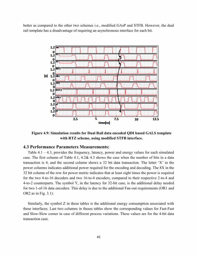
45
better as compared to the other two schemes i.e., modified GAsP and STFB. However, the dual
rail template has a disadvantage of requiring an asynchronous interface for each bit.
Figure 4.9: Simulation results for Dual Rail data encoded QDI based GALS template
with RTZ scheme, using modified STFB interface.
4.3 Performance Parameters Measurements:
Table 4.1 – 4.3, provides the frequency, latency, power and energy values for each simulated
case. The first column of Table 4.1, 4.2& 4.3 shows the case when the number of bits in a data
transaction is 4, and the second column shows a 32 bit data transaction. The letter ‘X’ in the
power columns indicates additional power required for the encoding and decoding. The 8X in the
32 bit column of the row for power metric indicates that at least eight times the power is required
for the two 4-to-16 decoders and two 16-to-4 encoders, compared to their respective 2-to-4 and
4-to-2 counterparts. The symbol Y, in the latency for 32-bit case, is the additional delay needed
for two 1-of-16 data encoders. This delay is due to the additional Fan-out requirements (OR1 and
OR2 as in Fig. 3.1).
Similarly, the symbol Z in these tables is the additional energy consumption associated with
these interfaces. Last two columns in theses tables show the corresponding values for Fast-Fast
and Slow-Slow corner in case of different process variations. These values are for the 4-bit data
transaction case.

46
Table 4.1: Measurement values of modified GAsP interface using 1-of-N encoding
S.NO Measurement 4-bit 32-bit SS Corner FF Corner
1
Clock
Frequency
(without
pausing)
1.19 GHz 1.19GHz 1.02GHz 1.48GHz
2 Latency .75ns .75ns+Y .82ns .64ns
3 Power 2.75mW+X 22mW+8X 2.20mW 5.68mW
4 Energy 14.17mJ
(4-bit )
14.17mJ+Z
(4-bit ) 8.64mJ 17.15mJ
It is observed that the modified STFB interface consumes least power. Change in power
dissipation due to the process variation ranges from 20.81% to 82.85%, with the modified RSDL
interface has the least and the modified GAsP interface has the most variation. Further it is seen
from these results that latency wise modified STFB is better. Process variations altered the
latency up to the 12% in modified GAsP interface, 15 % for the modified STFB interface and
11% for the modified RSDL interface. It can be observed that the modified RSDL interface is
most tolerant to process variations.
Table 4.2: Measurement values of modified STFB interface using 1-of-N encoding
S.NO Measurement 4-bit 32 bit SS Corner FF Corner
1
Clock
Frequency
(without
pausing)
1.14GHz 1.14GHz 995MHz 1.46GHz
2 Latency .71ns .71ns+Y .81ns .60ns
3 Power 2.45mW+X 19.6mW+8x 1.94mW 4.48mW
4 Energy 4.83mJ
(4- bit)
4.83mJ+Z
(4-bit) 4.08mJ 12.36mJ

47
Table 4.3: Measurement values of modified RSDL interface using dual rail encoding
S.NO Measurement 4-bit 32-bit SS Corner FF Corner
1
Clock
Frequency
(without
pausing)
1.18GHz 1.18GHz 970MHz 1.47GHz
2 Latency .55ns .55ns+Y .59ns .46ns
3 Power 2.55mW+X 20.4mW+8x 1.96mW 3.15mW
4 Energy 12.15mJ
(4-bit)
12.15mJ+Z
(4-bit) 8.81mJ 15.21mJ
Table 4.4 shows an overview of the interfaces described in the Chapter 3. Performance wise,
the RSDL outperforms other two interfaces. It shows the improvement of 26.66% and 22.5% as
compared to the GASP and STFB respectively. But the STFB is better in the power and energy
consumption.
Table 4.4: Comparison of modified GAsP, STFB &RSDL interfaces (for 4 bits of data)
Interface Frequency
(GHz)
Latency
(ns)
Power
(mW)
Energy
(mJ)
Modified
GASP 1.19 .75 2.75 14.17
Modified
STFB 1.14 .71 2.45 4.83
Modified
RSDL 1.18 .55 2.55 12.15
4.4 State of the Art GALS Systems:
Table 4.5 shows important performance parameters of contemporary state-of-the-art GALS
systems, utilizing FIFO on bundled data protocol based and pausible clocking on delay
insensitive based protocol. It can be seen that the latency insensitive based design allows the data
transfer at every clock cycle but at the expense of low clock frequency to accommodate the
overhead of FIFO signals. The second row in Table 4.5 indicates that the GALS wrapper in [67]
allows 2.87 GHz frequency, which is close to what we made our design to work at. However,

48
this design is customized to cater the need of the particular interface and the information related
to the pausing is not provided. The latency of about 900 ps will require this system to pause more
often. The last two rows in Table 4.5 show two GALS systems implementation on the FPGA,
certainly they are slower in terms of timing constraints because of the FPGA implementation.
This shows that GALS system is a viable option for the inter-module communication in MCD
system-on-chip (SoC).
Table 4.5: Performance Parameters of State-of-the- art GALS Systems
SYSTEM/Interface GALS
Approach Protocol
Operational
frequency
Power
consumption
Timing
constraints Technology
Wrapper for
Latency insensitive
system [66]
FIFO Bundled
data 2-
phase
333MHz -- Latency
insensitive
130nm
GALS QDI wrapper
for NoC [67] Pausible
clock
Delay
insensitive
2.87GHzsender-
2.59GHz
receiver
828uWsender-
819uW
receiver
907ps-
947ps
180nm
Asynchronous
interface for
Transreceiver on
FPGA [68]
FIFO
4-phase
bundled
data for
128 point
FFT
processor
577MHz -- 200Mbps ALTERA
Stratix III
GALS
implementation
over FPGA [69]
FIFO
2-phase
Bundled
data
protocol.
Less than
700MHz
-- 550MDI/s Spartan-3
Vertix 4

49
CHAPTER 5
CLOCK DOMAIN CROSSING (CDC) IN 3-D ICs
This chapter investigates various challenges associated with the incorporation of two classes of
widely used clock domain crossing techniques in 3-D ICs. Two CDC techniques includes; an
QDI based GALS technique, and loosely synchronous interfacing technique (such techniques are
described in literature [70] [71]). For simulation purposes, without losing generality, quasi delay
insensitive (QDI) protocol based pausible clocking is used as representative technique for the
first category (asynchronous interfacing) of CDC technique. While for the second category
loosely synchronous interface is used. In this Chapter, first CDC technique is called as QDI-
based GALS interface. In the same way, self-test self-synchronization (STSS) circuit [71] is used
as a representative technique for the second class of CDC technique (loosely synchronous) which
called as STSS based interface throughout rest of the chapter.
5.1 3-D IC Clock Domain Crossing in Multiple Tiers: This section provides the implementation details of two types of CDC techniques, i.e., QDI-
based GALS interface and STSS interface, from the perspective of 3-D ICs. Representative
designs, from each class of CDC technique, are analyzed along with their sequence of
operations.
5.2 QDI Based GALS CDC Technique: 3-D IC implementation details of CDC technique which uses QDI-based GALS interface in
conjunction with the plausible clocking are explained. Fig. 5.1 shows one such possible
implementation. There could be other architectures to implement with some minor modifications
to Fig. 5.1, and some of the implementation architectures will be discussed later. This CDC
technique is spread across two logic-tiers communicating with each other as shown in Fig. 5.1.
At Tier 1, the SSM (Synchronous Sending module) sends the encoded data signals (RS (0) to RS
(N-1)) through an asynchronous DI interface. At Tier 2, this encoded data is received by the
SRM (Synchronous Receiving Module).
Here, the QDI based GALS interface uses 1-of-4 data encoding. However, Dual Rail
encoding can also be utilized as described in the Chapter 2. One-of-4 encoding can be
implemented using various other asynchronous interfaces [63] [64] [65]. In this particular work,
we used modified version of GAsP and further details are given in [63]. The asynchronous
switching interface at Tier 1 takes data from SSM and passes it on to the Tier 2. ACK2 signal
enables or disables the switching interface to pass on the data. Data (RR (0) to RR (N-1)) at Tier
2 is received by SRM (Synchronous Receiving Module). Other components at Tier1 and Tier 2
include ME_S and ME_R on each tier. They are called as mutually exclusive elements, which in
turn control their respective Clk1 and Clk2 signals. At Tier 2, Req_Gen block is used to pass the
ready signal from the receiver side.

50
SSM
Inte
rfa
cin
g
Me
cha
nis
mClk1
Rst1
OR1
RS(0)
RS(N-1)RR(N-1)
RR(0)
Ready
Clk2ME_S
Req_Rcv
Clk1
Rst2
ACK2Req.Gen.
Receiver End
SRM
RR(0)
RR(N-1)
OR2
Clk2
Rst2
ME_R
Rst1
ACK2
Clk2
ACK2
TIER1 TIER2
ACK2
Sender End
RR(0)
RR(N-1)
Out_1
Figure 5.1: Architecture of the QDI based GALS interface CDC technique in 3-D ICs
5.2.1 Sequence of Signals
From 3-D perspective the QDI-based GALS interface is implemented as follows: Tier 1 contains
the SSM and interfacing mechanism along with the ME_S and ring oscillator, whereas Tier 2
contains the SRM along with ME_R, Req_Gen block and ring oscillator. Such a placement for 3-
D implementation is beneficial for pull channel based implementation because the data request is
initiated from the receiver or Tier 2 side. It requires TSV for encoded data signals (using return-
to-zero (RTZ) signaling protocol) and ACK2 signals only. Rst1 is generated at Tier 1, as can be
seen in Fig. 5.1. Signal transition graph (STG) and the waveforms are given in Fig. 5.2 and 5.3
respectively, provides an illustration for the QDI based GALS interface. Sequence of the events
is described below:
Idle State Requirement:
Initially, due to the implementation of RTZ signaling protocol, all signals at Tier 1 are
considered at logic zero.
Data transfer:
According to 1-of-N encoding, one RS(x) signal is asserted (1-of-N encoding), here x
represents any number from 0 to (N-1), RS (x) assertion stops the Clk1 signal through the
ME_S element.
At Tier 2, assertion of Req_Rcv signal stops Clk2 via the ready signal. As a result, ME_R
sends the ACK2 signal to Tier1, which is an indication that the receiver is ready to
receive data. Prior to the assertion of ACK2, sender could not send data.
Switching interface is enabled through the assertion of ACK2 and data goes through the
switch, passing through the TSV to SRM in the form of (RR(x)) signals.

51
Data Completion:
RR(x) signal reception (data completion) on SRM leads to the generation of Rst2 pulse to
bring the Req_Rcv signal down and release the Clk2.
Rst1 pulse, which allows CLK1 to restart, is generated as soon as completion of the data
is acknowledged via the ACK2 signal.
Clk1
RS(x)
Req_Rcv
Clk2
ACK2
RR(x)
Rst2
Rst1
Figure 5.2: Operation of QDI based GALS interface CDC technique using DI protocol
5.2.2 Explanation of State Transition Graphs (STG):
Two state transition graphs are provided in Fig. 5.3 to illustrate how each individual tier
works. The signal transitions related to Tier 1 of Fig. 5.1 are shown in Fig. 5.3(a). These
transitions are described as follows:
Tier 1 STG:
Idle state S10, is the state where all the control signals at Tier 1 are at logic zero level just like
RTZ (return to zero) , and Clk1 runs freely (SSM works normally).
Next, S10 to S11 transition shows the start of data transfer. In the assertion of RS(x) i.e., the data is
asserted to pass through the asynchronous switching interface. The Tier 1 transits from S10 to S11
state.
S11 to S12 transition indicates that Clk1 has paused and the sender tier has stopped. This occurs as
a result of assertion of RS(x), which results in pausing Clk1 through ME_S, hence stopping the
sender end.
S12 to S13 transition causes triggering of the asynchronous interface to transfer data, courtesy to
the assertion of ACK2 signal.

52
With S13 to S14 transition the completion of data transaction begins. Due to the ACK2 signal, the
RR(x) signal gets asserted and Rst1 pulse (shown as small pulse in Fig. 5.3(a)) is generated.
During S14 to S10 transition Tier 1 returns back to its idle state S10, with resetting the RS(x) data
signals and releasing the Clk1 signal (hence the clock pulses are shown in Fig. 5.3(a).
Tier 2 STG:
Sequence of the operations at Tier 2 of Fig. 5.1 is shown in Fig. 5.3(b) with the help of signal
transition graph. Description of these transitions is as follows:
S20 is an idle state, where all signals are zero until the request for data is received. Clk2 runs
freely hence, SRM works normally at Clk2 signal frequency. State S20 to S21 transition at Tier 2
indicates that the request for the data (Req_Rcv) has been received which is an indication of
SRM in receiving mode.
State transition from S21 to S22 occurs when ACK2 signal get asserted as a consequence of the
assertion of Req_Rcv, and it (Req_Rcv) also pauses the Clk2 signal through ME_R block at Tier
2 (shown in Fig. 5.1).
Assertion of RR(x) signal causes S22 to S23 transition that is the corresponding receiver side
signal of the sender data (RS (x) via asynchronous switching interface. S23 to S24 state transition
indicates that receiver has received data (RR(x)), and the Rst2 pulse is generated through this
received data. S24 to S25 transition shows the beginning of the completion of the data transaction,
as Rst2 pulse results in the negation of Req_Rcv signal by resetting the Req_gen block shown in
Fig. 5.1.
S25 to S20 transition indicates the completion of data transaction as after the negation of Req_Rcv,
ACK2 signal is negated and Clk2 signal is released. SRM (shown in Tier 2 of Fig. 5.1) resumes
the normal operation.
S10
S11
S12ACK2 +
Clk1 -
S13
RS(x) +
Rst1
Clk1 S14
RR(x) +
RS(x) -( )
( )
Figure 5.3(a): Tier 1 signals transition sequence

53
S20
S21Req_Rcv +
S22
ACK2 +Clk2 -
S23RR(x) +
S24
S25
Rst2
Clk2
Req_Rcv -
ACK2-
( )
( )
Figure 5.3(b): Tier 2 signals transition sequence
Figure 5.3: Operation of QDI based GALS interface CDC technique
on state transition diagram
5.3 STSS Interface based CDC in 3-D ICs:
This section provides details on implementation of another class of CDC technique, i.e., STSS
interface based CDC (a representative design for loosely synchronous technique), to do the
interlayer communication in 3-D IC. Fig. 5.4 shows the CDC implementation of STSS interface.
D-F
LIP
FLO
P
D-F
LIP
FLO
PD QD Q
FIFO
DELAY MATCH
ACKCONTROL
LOGIC
Cs CLK2
Cs=CLK1 or CLK2
DATA
TEST
TIER 2
DA
TAA
CK&
REQ
Reg. 1
Reg. 2
Reg. 3
Reg. 4REQ
DA
TA
TIER 1
CLK
Figure 5.4: Architecture of STSS interface for CDC (Clock Domain Crossing) in 3-D IC

54
Number of signals, to and from the sender or the receiver is always equal for this case. In terms
of TSV utilization (explained in Section 5.2), the STSS interface implementation can be
implemented either at the sender or the receiver end, both cases require equal number of TSVs.
In this particular work, it is implemented on the sender end. Closer inspection of Fig. 5.4, shows
that only ACK, REQ, CLK and DATA signals require TSVs.
5.3.1 Sequence of Signals:
The sequence of signals for STSS interface based CDC is explained based on a pull channel
implementation, i.e. request (REQ) is initiated from the receiver, which is on Tier 2 as shown in
Fig. 5.4. Acknowledgement (ACK) signal is asserted at the sender end in response to the receiver
request (REQ) signal. Assertion of ACK signals starts data transfer. On Tier 2 data is received
and ACK is negated, which indicates that the data has been received. REQ and ACK signals are
negated to complete the data transaction using 4-phase RTZ (return to zero) protocol. This
sequence of operations is illustrated in Fig. 5.5 through the waveforms; the arrows represent
causality among the signals.
CLK
REQ
ACK
DATAValid Data
TIER2
TIER1
Figure 5.5: Operation of STSS interface CDC technique
5.3.2 Explanation of State Transition Graph (STG):
Protocol of STSS interface (Fig. 5.4) is described using state transition graph for the whole
system. As shown in Fig. 5.6, assertion of REQ signal indicates that the receiver at Tier 2 is
ready to receive data, state transition occurs between S0 to S1. The transition from state S1 to S2
shows that sender has asserted the data on data lines in response to the request (REQ) signal.
S0
S1
S2
DATA
S3
DATA -REQ -ACK -
REQ+
ACK+
Figure 5.6: STG of CDC using STSS interface

55
After the assertion of data, the ACK signal also gets asserted from the sender (Tier 1) side, as an
indication of valid data and the sender transits from state S2 to S3. The system is brought back to
idle state S0, with the negation of ACK, REQ and DATA signals at the completion of data
transfer.
5.4 TSV Redundancy:
TSVs are vulnerable to fracture, which in turn lead to the lower yield. To improve the yield of
3-D ICs, researchers have proposed various TSV redundancy techniques [72][73][74]. The
overall improvement in the yield for 3-D ICs is directly related to the ratio of the signal carrying
TSVs to the available redundant TSVs. So, 1st order TSV estimation is required, to utilize TSVs
smartly. A mathematical relationship is provided to obtain effective redundancy and hardware
design overhead. It is found that when signals are more uniformly spread across the TSV cells,
then the effective redundancy improves. In this section, an overview of different TSV
redundancy techniques is provided along with their allocation methodology, in case of TSV
failures. Furthermore, Section 5.4.1 analyzes, for practical realization, four data bits transfer in 3-
D ICs across different tiers is considered. In Section 5.4.2, required number of TSVs is
illustrated for each redundant TSV allocation methodology, under different data encoding
schemes for QDI based GALS interface and STSS interface.
5.4.1 Types of TSV Redundancy Architecture:
Due to TSV susceptibility to fracture, different redundant TSV architectures have been
proposed in the literature [72][73][74]. These techniques have different levels of failure tolerance
at the expense of design complexity. This sub-section provides an overview of three widely used
TSV redundancy techniques.
Before providing the details of these techniques, Fig. 5.7 illustrates different symbols that
have been used in figures (Fig. 5.8 – 5.11) related to TSV redundancy.
Signal TSV
1-3 Switch
Redundant TSV
1-2 Switch Routers
Signal Pad
Figure 5.7: Various symbols used in Fig. 5.8 to 5.11
One:4 TSV Redundancy [72]:
This redundancy technique adds one extra TSV for group of four TSVs as shown in Fig. 5.8.
One: 4 TSV redundancy technique can tolerate up to one TSV failure within a group of four
signal carrier TSVs (as shown in Fig. 5.8). In this configuration, if a TSV fails then signal
corresponding to that failed TSV signal is shifted to the next neighboring TSV and this
arrangement is propagated until it reaches the last (spare) TSV.

56
TIER 2
TIER 1
Figure 5.8: One:4 TSV redundancy [72] across two tiers for 4-bit data transfer
As a standard cell library based designs, it is desirable that TSV redundancy architecture
shown in Fig. 5.8 is used as one cell in the library. The following analysis explains how many of
such 1:4 TSV redundancy cells (shown in Fig. 5.8) are required to transfer X number of signals
across the tiers. For example, in total X signals need to be sent from Tier 1 to Tier 2 using such
cells, then total cells required for the X signals using 1:4 TSV redundancy architecture can be
written in the form of Eq. (5.1).
1:4 TSV Cells Required =
4
X (5.1)
Each cell of 1:4 TSV redundancy has minimum one spare TSV for fault tolerance, however
when all four available signal TSVs are not in use, they can also be considered as redundant
TSVs. In such a case, fault tolerance is more than one. Suppose within each 1:4 TSV redundancy
cell, Y number of signal TSVs for signals transportation across tiers are being used. We know
that maximum four signals can be transferred using one block and each block contains one
redundant TSV. Fault tolerance of individual 1:4 TSV redundancy cell can also be generalized in
form of Eq. (5.2).
Fault Tolerance = [4-Y] +1 (5.2)
Consider a case, when three signal TSVs (Y=3) of a 1:4 TSV redundancy cell are being used.
If we put Y=3 in Eq. (5.2) then fault tolerance of that particular 1:4 TSV redundancy cell comes
out two.
Fault tolerance is about redundant TSV per cell. In same way, average number of TSVs for a
particular number of signals say X can determined. Suppose for the X signals minimum cells are
required can be determined using Eq. (5.3). Signals allocated to each cell can be different in
different cells, which mean that each call will have a specific fault tolerance capacity (Eq. 5.4). If
fault tolerance capacity of all cells, means redundant TSVs (Redi) are summed up and divided to
blocks required to send the X signals (Eq. 5.3), then average number of redundant TSV per cell
can be written in form of Eq. (5.3).

57
Average Redundant TSV/cell=
(5.3)
It is also imperative that how the signals are distributed into different TSV cells, because the
efficient distribution of signals can improve the overall fault tolerance. As an example, consider
5 signals have to be transferred across two tiers through 1:4 TSV cells. Therefore, two 1:4 TSV
redundancy cells (Eq. 5.1) are needed. The distribution of these signals can take any of the
following two different possibilities: one cell with four signals and other cell with one signal, and
one cell with three signals and other cell with two signals.
As a comparison of different possibilities with reference to 1:4 TSV redundancy cell,
Effective RedI/Cell can be obtained for two of the above possibilities by averaging the number of
available redundant TSVs signals in each of the above possibilities for 4 signal TSVs. For the
first possibility: (1×4+ 4×1)/5 = 1.6, it means it has effective RedI/Cell of 1.6. The second
possibility: (2×3+3×2)/5 = 2.4, it has effective RedI/Cell of 2.4. It shows that the second
possibility has more effective RedI/Cell value than the first possibility, so the second possibility
has more effective redundant TSV distribution per cell. The second possibility will provide
maximum number of cells, with fault tolerance of more than one.
To generalize the calculation of each possibility of 1:4 TSV redundancy cell using the above
analysis is as: Suppose Redi is the number of redundant signal in ith cell and Sigi is number
signals in that cell. For all signals, weight for each possibility of signal distribution across
different cells can be written in form of Eq. (5.4).
Effective RedI/Cell =
(5.4)
Eq. (5.4) can be expanded further by evaluating the number of cells required (n) and redundant
signals (Redi) of each cell. Both parameters can be calculated based on Eq. (5.2 & 5.3). If we
insert parameters into Eq. (5.4), then it can be represented by Eq. (5.5) for ith cell passing Yi
signals.
Effective RedI/Cell =
(5.5)
Where n=
4
X

58
Two:4 TSV Redundancy [73]:
Another TSV redundancy technique is based upon 2:4 allocation, where each group of four
signals has two redundant TSVs as shown in Fig. 5.9. The shaded TSVs are used under the
normal circumstances. If one of the two top (bottom) TSVs fail that it is re-routed through the
top (bottom) redundant TSV. This technique can tolerate up to two failures in the group of four
signal TSVs.
TIER 2
TIER 1
Figure 5.9: Two:4 TSV redundancy [73] across two tiers for 4-bit data transfer
In order to analyze that how many 2:4 TSV redundancy cells (Fig. 5.9) are required to transfer
the signals. Let us suppose, there are X number of signals across tiers and each 2:4 TSV
redundancy block can carry maximum four signals. Eq. (5.1) also explains number of blocks of
Fig. 5.9, required to transfer the X signals. Block requirement of both 1:4 and 2:4 TSV
redundancy cell is based on same equation i.e., Eq. (5.1) because of fact that both redundancy
cells have same number of signal TSVs in one block. If there are 13 signals to transfer (X=13, in
Eq. 5.1) then four cells of 2:4 TSV redundancy architecture would be required.
Furthermore, fault tolerance of 2:4 TSV redundancy architecture, is little bit different than
that of 1:4 redundancy architecture. Suppose Y signals are being transferred using 2:4 TSV
redundancy cell. As one 2:4 TSV redundancy cell has two dedicated spare TSVs and it can pass
maximum of four signals. If Y signals are sent then Eq. (5.6) describes the failure tolerance of
this particular cell.
Fault Tolerance = [4-Y] +2 (5.6)
For example, there are three signals (Y=3) in a 2:4 TSV redundancy cell. So Eq. (5.6) describes
fault tolerance as three for this case.
Number of average redundant TSVs per cell can be calculated using Eq. (5.3), where signal
are allocated to each cell. Redundant TSVs for each cell can be calculated using Eq. (5.6). These
redundant TSVs are summed up and divided by the number of 2:4 TSV redundancy cells

59
required to transfer all of the available signals (Eq. 5.1). For example, there are six signals,
according to Eq. (5.1) we require two 2:4 TSV redundancy cells. The cells will have tolerance of
two and four, if four and two signals are passed through them (Eq. 5.6) respectively. If we put
these values in Eq. (5.3), there will be three redundant TSVs per cell on average. Range of
redundant TSV per call can also by determined, based on fact that minimum there are two
redundant TSVs per cell and on the other side at least one TSV should be in use in a cell, it
provides five redundant TSVs. So, average number of TSVs for 2:4 TSV redundancy cell would
always be from two to five.
For the transfer of signals that require more than one cell, in general there are different
possibilities through which different number of signals can be assigned to each cell. To calculate
which combination is most optimal one, we have to define effective RedI/Cell for each
possibility. Possibility with higher effective RedI/Cell value is the best choice as it provides more
fault tolerance in maximum number of cells. Eq. (5.4) can also be applied for 2:4 TSV
redundancy cell, if we put value of Redi based upon Eq. (5.6) and n from Eq. (5.1). Then Eq.
(5.7) can be written for 2:4 TSV redundancy ith cell with Yi signals as;
Effective RedI/Cell =
(5.7)
Where n =
4
X
Continuing from previous example, for six signals two possibilities are as: one cell with four
signals and second cell with one signal, and each cell with three signals. If we put the number of
signal TSVs in Eq. (5.7) for each possibility. It gives effective RedI/Cell value of 2.17 and 3
respectively. It means second option is more suitable as it will provide much balance fault
tolerance distribution for this case.
Router Based TSV Redundancy [74]:
Router based redundancy approach is proposed in [74] shown in Fig. 5.10. It is called router
based redundant TSV due to the involvement of routers in redundant path allocation.
Figure 5.10: Router based redundancy: 3×3 architecture [74]

60
Router based redundancy allocation technique is different from earlier two techniques as it is
based on the premise that if one TSV fails then likelihood of the failure of neighboring TSV
would also increase. So instead of routing failed TSV signal to a neighboring TSV it re-routes
signal path to a distant TSV. Redundant TSV allocation mechanism is further explained in Fig.
5.11 with the help of an example.
Router based redundant TSV allocation for the four data bits transfer is shown in Fig. 5.11. In
case the TSV A fails, then this redundancy block re-routes the data to the TSV B which is not
neighboring to the TSV A. Obviously, the added resilience is obtained at the expense of more
delay and area overhead in hardware. Addition of the extra hardware also leads towards more
power and energy consumption.
A
TIER 1
TIER 2
B
Figure 5.11: Router based redundant TSV [74] allocation across two tiers
for 4-bit data transfer
Generalization of router based TSV cell requirement can be done as: For example there are
the X signals that need to be traversed from Tier 1 to Tier 2 and we can use any m×n
implementation (like Fig. 5.10 represents 3×3 architecture). Based on above two parameters Eq.
(5.8) can be written to describe how many cells of that particular m×n are required. Consider a
case where 25 data signals needs to be transferred by using 3×3 architecture. We know that each
3×3 architecture can transfer maximum nine signals (as 3×3= 9). So for 25 signals (X=25),
according to Eq. (5.8) three 3×3 architecture cells would be needed.
Blocks Required =
nm
X (5.8)
For the Y number of signal TSVs being used in a cell, to transfer the signals in a particular
m×n architecture. Fault tolerance of that m×n architecture can also be written in form of Eq.

61
(5.9). Maximum m×n signals can be transferred through one cell using the router based
redundancy architecture and each cell contains m+ n redundant TSVs. Now, consider an example
with eight data signals being transferred using a 3×3 router based architecture block. By
plugging in these values into Eq. (5.9), fault tolerance comes out as seven.
Fault Tolerance = [(m×n) -Y] + (m + n) (5.9)
The average number of redundant TSVs per cell for the case of router base redundancy can be
calculated using Eq. (5.3). In Eq. (5.3) redundant TSVs for each m×n cell, the number of m×n
cells required for X signals should be calculated using Eq. (5.8) and (5.9). Now, consider transfer
of 13 signals; two 3×3 cells (Eq. 5.8) would be sufficient. In all, there are three choices: nine
signals from one cell and four signals from other cell, seven signals from one cell and six signals
from other cell, and eight signals from one cell and five signals from second cell. If fault
tolerance of each cell is calculated using Eq. (5.9) it comes as: six and eleven, eight and nine, and
seven and ten respectively. Putting in these values in Eq. (5.3), 8.5 is average number of TSVs
per cell. Range of average number of TSVs per cell for a particular m×n cell is from m +n to (1-
((m×n)- m+ n)), according to the minimum number of available TSVs and the least number of
TSVs in use, in each cell.
Taking Yi signals transfer through ith cell as an example; we can calculate effective RedI/Cell
value for each possible combination by expanding Eq. (5.4) based upon router based cell
parameters, to evaluate which choice is more considerable. Eq (5.10) can be expressed as;
Effective RedI/Cell =
(5.10)
Where n =
nm
X
Taking same example of 13 signals transfer as mentioned above, weight of each choice comes as
7.54, 8.46 and 8.15 respectively. Values indicate that the second choice has more balanced fault
tolerance or redundant TSV distribution across the two blocks.
5.4.2 TSV Requirement in CDC Techniques:
3-D IC requires TSVs for CDC from one tier to the other tier. Requirement of TSVs to
transfer the four data bits from Tier 1 to Tier 2 of Fig. 5.1 are detailed in this subsection. QDI
based GALS interface, may utilize any type of DI code. Among many possible codes choices, we
analyzed three most widely and effectively used DI data codes, which are 1-of-N, dual-rail, and
3-of-6 (m-of-n) encoding. STSS interface does not require any data encoding, because it is not
utilizing any DI code as requirement of communication protocol.

62
5.4.2.1 TSV Requirement without Redundancy:
Overall, 16 data signals are required to transfer the four bit data using 1-of-N encoding (as
this is a one-hot or cold encoding) and one control signal, which is ACK2 signal as shown in the
Fig. 5.1. So, in total 1-of-N encoding requires 17 TSVs without using any redundancy
architecture, as shown in row 1 of Table 5.1. In similar way, 3-of-6 encoding has 3 asserted
signals at a time, out of 6 signals. The transport of four data bits using 3-of-6 encoding requires
six data signals and one control signal (ACK2), i.e., in all it requires seven signals transfer using
TSVs from one tier to another tier (row 1 column 2 in Table 5.1). For dual rail encoding, each
data bit is encoded into two bits. Therefore, overall eight signals for data and one control signal
are required to transfer four bits of data using dual rail encoding (row 1 column 3 in Table 5.1).
QDI based GALS interface has local clocks on each tier (Fig. 5.1), therefore no clock signal
transfer is required across tiers.
As shown in Fig. 5.4, STSS interface requires four data signals for four data bits and three
control signals, which include REQ, ACK and CLK signals. In case of no redundancy seven
TSVs suffice the need of data transactions across tiers of Fig. 5.4. In general, for no redundancy
number of signals will always equal to number of TSVs but there would be no failure tolerance.
5.4.2.2 TSV Requirements with State-of-the-Art Redundancy Techniques:
An analytical comparison based on number of TSVs for mentioned three codes is provided in
Table 5.1 against each TSV allocation technique.
One:4 TSV Redundancy [72]:
QDI based GALS interface, for 1-of-N encoding case, according to Eq. (5.1), five cells of Fig.
5.8 would be required for the 17 signals. There are three different possibilities through which the
17 signals can passed across tiers using five cells of 1:4 TSV redundancy. Fault tolerance (Eq.
5.2) is also mentioned for each possibility.
i) Four cells with four signal TSVs and one cell with one signal TSV with fault
tolerance of one and four respectively
ii) Two cells with four signal TSVs and three cells with three signals TSVs. Fault
tolerance is one and two respectively
iii) Three cells with four signal TSVs and each cell with one fault tolerance, one cell with
three signals and two as fault tolerance and one cell with two signal TSVs (fault
tolerance two)
Average number of redundant TSVs per cell of each possibility can be found by utilizing Eq.
(5.3). On the average, there are 1.6 redundant TSVs for each possibility. Among three options,
effective RedI/Cell value of each possibility (Eq. 5.5) is as; 1.18 for the first, 1.53 for the second
and 1.41 for the third (Table 5.2) possible combination. The second option is most optimal due to
the high effective RedI/Cell value as compared to other two options.

63
Whereas, for 3-of-6 encoding, seven signals needs transfer across tiers, by using Eq. (5.1) two
units of 1:4 redundancy cells (shown in Fig. 5.8) are required, i.e., ten TSVs are needed in total.
These TSV numbers are tabulated in row 2 of Table 5.1. Out of two units, one unit will pass
three and the other unit will pass four signals. As this is the only possibility for signal allocation
using 1:4 TSV redundant cells, so average number of redundant TSVs (Eq. (5.3)) comes out 1.5
(Table 5.2). According to Eq. (5.2), fault tolerance would be one for cell passing four signals and
two for cell passing three signals. Lastly, dual rail encoding can transfer the same number of data
bits using eight encoded bits, and one control signal. By put in values of X= 9 in Eq. (5.1), three
block are required. For three blocks, three different options for the signal transfer are as:
i) Two cells with four signals and one cell with one signal
ii) One cell with four, second cell with three and third cell with two signals only
iii) All three cells with three signals passing through each of them
Similarly, fault tolerance of each individual cell can be found through the Eq. (5.2). By
plugging in (Y= 1, 2, 3 &4) in Eq. (5.2) fault tolerance will be four, three, two and one
respectively, according to the number of signals being passed through each block. The average
number of redundant TSVs per cell using Eq. (5.3) for each of above possibility is same i.e., 2.
According to Eq. (5.5) the effective RedI/Cell value of each possibility for above mentioned
sequence is 1.33, 1.78 and 2 respectively.
On the other hand, two cells of 1:4 TSV redundancy are required for seven signals in STSS
interface CDC using Eq. (5.1). Where, one block will have fault tolerance of two as it is using
three signal TSVs (Eq. (5.2)), while the other block has fault tolerance of one (four signals).
Average number of redundant TSVs per cell is 1.5 using Eq. (5.3).
Table 5.1: Number of TSVs required for CDC Techniques
QDI Based GALS
Interface STSS Interface
Encoding 1-of-N
Encoding
3-of-6
Encoding
Dual rail
Encoding
No
Encoding
No
Redundancy 17 7 9 7
Redundancy
1:4 [72] 25 10 15 10
Redundancy
2:4 [73] 30 12 18 12
Redundancy
Routers [74] 30 15 15 15

64
Two:4 TSV Redundancy [73]:The number of cells required is same for each data encoding
as that of the 1:4 TSV redundancy because of same number of signal TSVs in each cell of the 1:4
and 2:4 TSV redundancy. Two:4 TSV redundancy cells requirement for different encodings of
the QDI based GALS interface based upon Eq. (5.1) is as: One-of-N encoding requires five
blocks i.e., 30 TSVs to transfer the four data bits. There are three different possibilities of signals
to transfer through each cell. These three possibilities are same as described for the 1-of-N
encoding in 1:4 TSV redundancy of Section 5.4.1. On the average there are 2.6 redundant TSVs
per cells (Eq. 5.3). However, fault tolerance of each block using Eq. (5.6) is as;
i) Five for cell passing one signal through it
ii) Four for cell passing two signals through it
iii) Three for cell passing three signals through it
iv) Two for cell passing four signals through it
Using Eq. (5.7) each possibility has weight of 2.18, 2.53 and 2.41, which means the second
possibility is most appropriate as compare to other two possibilities.
Three-of-6 encoding requires 2 blocks similar to the Fig. 5.9 (which means 12 TSVs), the
only option is, one block with all four signal TSVs used and other block with three signal TSVs
used. Later block will tolerate up to three failure (put Y=3 in Eq. 5.6). However, average
redundant TSVs per cell come out to be 2.5, by using Eq. (5.3). Dual rail encoding requires 18
TSVs (3 blocks similar to Fig. 5.9). These TSVs numbers are tabulated in row 3 of Table 5.1.
Three different options of signal allocations to each specific cell are same as described earlier for
1:4 TSV redundancy, for the same encoding. There are three redundant TSVs (Eq. 5.3) per cell.
The effective RedI/Cell value, using Eq. (5.7) for three different possibilities for 2:4 redundancy
case are as: 2.33, 2.78 and 3 respectively (Table 5.2). Again, the second possibility is more
suitable in terms of fault tolerance per cell.
Whereas, STSS based interface for CDC requires only 12 TSVs i.e., two cells (Eq. 5.1). One
cell will have fault tolerance of two, as all signal TSVs are in use. While, the second cell has
only three signal TSVs are being used, so it will have fault tolerance of three (Eq. 5.6). However,
1.5 is the average redundant TSVs per cell (Eq. 5.3).
Router Based TSV Redundancy [74]:
The TSV requirement for the each data encoding based upon router based redundant TSV
allocation approach, is tabulated in row 4 of Table 5.1.
The QDI based GALS interface using 1-of-N encoded values to transfer the four bit data
across tiers, requires two 3×3 cells (Fig. 5.10) of the router based redundant TSV architecture,
because for this 17 signals need to be transferred across tiers. If we plug X=17, m=3 and n=3 in
Eq. (5.8) then bocks requirement comes out as two. Only one possibility: nine signals will pass
through the first block while eight signals will pass through the second block, if we evaluate fault

65
tolerance of both blocks using Eq. (5.9) then it comes as six and seven respectively. However, on
the average there are 6.5 redundant TSVs per cell (Eq. 5.3). Whereas one such 3×3 block (using
Eq. (5.8)) will be sufficient for the 3-to-6 encoded data, as it needs only seven signals. Fault
tolerance of this block would be eight, as in this case Y=7, m=3 and n=3 in Eq. (5.9). The cases
where one block is sufficient for signal transfer, average number of TSVs per cell, fault tolerance
and weight of possibility becomes equal. Evaluation of only one factor i.e., fault tolerance, is
required instead of evaluating three factors.
In last, dual rail encoding technique, one 3×3 block would be required to transfer the nine
signals, means 15 TSVs. These TSV numbers are indicated in the last row of Table 5.1. By using
Eq. (5.9) fault tolerance can also be calculated which is six in this case. In the same way, router
based redundancy allocation (Fig. 5.11) for STSS interface needs 15 TSVs means one 3×3 block
(Eq. (5.8)) as it needs only seven signals to transfer across tiers. On the other hand fault tolerance
using Eq. (5.9) (Y=7) is eight.
Table 5.2: TSV statistics using redundancy techniques
QDI Based GALS Interface
STSS Interface
Redundancy 1-of-N
Encoding
3-of-6
Encoding
Dual rail
Encoding
No
Encoding
Cell used
Average RedI/cell
Effective RedI/cell
Cell used
Average RedI/cell
Effective RedI/cell
Cell used
Average RedI/cell
Effective RedI/cell
Cell used
Average RedI/cell
Effective RedI/cell
Redundancy
1:4 [72] 5 1.6
(opt.1)1.18
(opt.2)1.53
(opt.3)1.41 2 1.5 (opt.1)
1.5 3 2
(opt.1)1.33
(opt.2)1.78
(opt.3) 2 2 1.5 (opt.1) 1.5
Redundancy
2:4 [73] 5 2.6
(opt.1)2.18
(opt.2)2.53
(opt.3)2.41 2 2.5 (opt.1)
2.5 3 3
(opt.1)2.33
(opt.2)2.78
(opt.3) 3 2 1.5 (opt.1) 1.5
Redundancy Routers [74]
2 6.5 (opt.1) 6.5 1 8 (opt.1) 8 1 6 (opt.1) 6 1 8 (opt.1) 8

66
CHAPTER 6
TIMING CHARACTERIZATION OF CDC TECHNIQUES
This chapter provides the timing characterization of both CDC techniques, which are
implemented using TSVs for both pull and push channel. TSV failure leads to the operational
delay within and between the data transactions. Our analysis caters for that. Delay is introduced
because of re-routing of failed TSV path to redundant path. Sometimes, added delay can cause
malfunctioning due to violation of some timing assumptions i.e., in STSS interface case.
Explanation of TSV failure for both the QDI based GALS interface CDC and the STSS interface
CDC is based upon 1:4 redundancy [72] technique, where failed TSV path is re-routed to the
next neighbor TSV.
6.1 QDI Based GALS CDC Pull Channel:
As explained earlier, in pull channel data request is initiated from the receiver side.
Explanation provided in the Chapter 5, on operation of QDI based GALS CDC technique is also
based on pull channel. Push channel base implementation of QDI based GALS CDC technique is
not possible, because of DI protocol requirement, as already mentioned in Section 5.1.
Here, timing characterization explanation of QDI based GALS CDC technique is based on the
first option of Rst1 pulse extraction i.e., in Fig. 5.1, where Rst1 signal is extracted at Tier1. There
are two options for extraction of Rst1 signal as shown in Fig. 6.1. Extraction of Rst1 at Tier1
saves the TSV required to transfer Rst1 signal across two different tiers.
In Fig. 6.1(a) it is shown that the ACK2 signal is traversed from Tier 2 to Tier 1 and Rst1
pulse is generated at Tier 1, in Fig. 6.1, this implementation is also shown. Another possibility is
shown in Fig. 6.1 (b), where the ACK2 signal and the Rst1 pulse both are generated at Tier 2 and
traverse over the TSV from Tier 2 to Tier 1. The consequences to two different implementations
are further elaborated in next Section.
ACK2 TIER2ACK2TIER1
ACK2
ACK2TIER2
ACK2TIER1
Rst1
Rst1Rst1
a) Rst1 extraction at Tier 1
b) Rst1 extraction at Tier 2
Rst1
Figure 6.1: Rst1 extraction options from ACK2 signal

67
6.1.1 Data (RR(x)) TSV failure:
QDI based GALS interface uses 1-of-N, m-of-n or dual rail data encoding techniques. All of
these encoding techniques allow one or few (m signals in m-of-n encoding) asserted data signals
and rest of the signals are negated (a requirement of RTZ signaling). To facilitate the
explanation, it is assumed that all the signals are active high. In 3-D ICs, the RR(x) signals are
carried over the TSVs, and if one of those TSVs fails then following three cases may arise:
I) Zero (Negated Signal) carrying TSV fails and failed TSV does not affect the path of logic ‘1’
(asserted signal) carrying TSV
II) Zero (Negated Signal) carrying TSV fails and failed TSV does affect the path of logic ‘1’
(asserted signal) carrying TSV
III) One (Asserted Signal) carrying TSV fails
The first case lead to no failure or incremental delay as logic ‘1’ carrying TSV is not being
affected. The signal re-routing to the redundant path would be after logic ‘1’ carrying TSV.
Thus, signal re-routing affects those signals that are after logic ‘1’ carrying TSV. Due to the data
encoding, only delay on logic ‘1’ carrying TSV is of our interest.
The other two cases affect the signal carrying path thus it will affect the timing characteristics
of the design. However, our analysis shows that the protocol still remains valid. It can be seen in
Fig. 6.2 that due to TSV redundant paths, data received at the receiver end (RR(x)) is delayed
(shown with the dotted lines in Fig. 6.2). Consequently, Rst2 pulse is delayed, which causes
delay in the ACK2 signal negation. Negation (RTZ) of ACK2 signal indicates the successful
completion of the data transaction.
Clk 1
RS(x)
Req_Rcv
Clk2
ACK2
RR(x)
Rst 2
Rst1
DATA RR(x) TSV Failure
Figure 6.2: QDI based GALS CDC technique if data RR(x) carrying TSV fails

68
6.1.2 Control Signal TSV failure:
In Fig. 5.1, it is considered that the switching interface is placed at Tier 1. So the only control
signal that is utilizing the TSV is ACK2 signal. The failure of which may lead to some delay in
signal propagation due to TSV redundancy techniques.
This leads to extra delay and added timing constraints for completing the data transaction in
the hardware as shown in Fig. 5.1. Fig. 6.3 shows the new timing constraints with dotted lines if
ACK2 signal TSV fails. It can be seen from the figure that due to the delay in ACK2 signal the
RR(x) data transaction started at a later time instant. Subsequently, the completion of the data
transaction is delayed. It is worth mentioning here that this increment in the delay does not lead
to any malfunctioning of the protocol.
Clk 1
RS(x)
Req_Rcv
Clk2
ACK2
RR(x)
Rst 2
Rst1
Control (ACK2)TSV Failure
Figure 6.3: QDI based GALS CDC technique if ACK2 signal TSV fails
6.1.3 Both DATA (RR) and control signal TSV failure:
The worst case possibility is that both of the data (RR(x)) and control signal TSVs fail
simultaneously. As in the case of isolated failures of data or control signals, the worst case TSV
failures also cause delay in operation only without introducing any malfunctioning, because of
interdependency of data and control signals in DI protocol.
Fig. 6.4 shows effects of both the data and control signal TSV failure. ACK2 signal delays
RR(x) signal, which is further delayed due to data TSV failure. Delay of both data and control
signals adds up and results in late generation of the Rst1 and Rst2 pulses.

69
Clk 1
RS(x)
Req_Rcv
Clk2
ACK2
RR(x)
Rst 2
Rst1
Control (ACK2) & DATA (RR(x))TSV Failure
Figure 6.4: Effect of Control and Data (RR(x)) signal TSV failure on DI protocol
As mentioned in Fig. 6.1(b) another option to implement this interface for 3-D IC is to extract
the Rst1 pulse at Teir 2 and traverse both the ACK2 and Rst1 signal through two different TSVs.
Following timing analysis discusses timing analysis for such a case. It can be noticed that data
signal TSV failure scenario remains the unchanged; therefore only control signal failure scenario
is explained below in Fig. 6.5.
Clk 1
RS(x)
Req_Rcv
Clk2
ACK2
RR(x)
Rst 2
Rst1
ACK2 TSV Failure
Figure 6.5: QDI based GALS CDC technique malfunctioning: ACK2 signal TSV fails
Control Signal Failure Scenario for the implementation shown in Fig. 6.1 (b): When the
TSV corresponding to the ACK2 signal fails then redundant TSV allocation would require

70
additional time to traverse the control signal. In such a case, QDI protocol does not allow the
data to pass on from RS(x) to RR(x) until the ACK2 signal reaches Tier 1, which enables the
switching interface. However, if only ACK2 signal carrying TSV fails then it is possible that
Rst1 signal reaches the Tier 1 before the ACK2 signal. Hence this condition can violate the
asynchronous protocol conditions, which in turn cause the data loss if not addressed at the design
time. Fig. 6.5 illustrates this phenomenon where RR(x) is not received due to additional delay in
the ACK2 signal (due to TSV failure), resulting in premature reset of the sender data and hence
causing data loss (no activity on RR(x) signal).
6.2 Timing Analysis of QDI based GALS CDC:
Although, redundant path allocation techniques are available but TSV failures affect the
overall operation of the system in various ways, such as increment in delay, and possibility of
erroneous operation. Hence, this section provides timing analysis of the scenarios discussed in
Section 6.1, so that timing bounds can be defined for the successful operation of such interfaces.
In Fig. 5.1, the QDI based GALS CDC technique, RR(x) and ACK2 (control signal) signals
are transferred through TSVs. On careful inspection it can be seen that the critical path in Fig.
5.1 is the path from request generation at Tier 2 to the final reception of RR(x) via generation of
the ACK2 signal (assuming no clock pausing at receiver) and passing through the asynchronous
switch (shown as interfacing mechanism in Fig. 5.1). This path is the longest from request
generation to data reception. It is assumed that RS(x) (Fig.5.1) is available at data lines (i.e., data
is ready to be sent). Any delay on this path can delay interface operation and hence will require
clock to pause. If TTRANSACTION indicates the complete latency of the path then total delay of the
critical path can be shown as follows:
TTRANSACTION = TReq_Rcv-to-ACK2 + TACK2-to-RR(x) + TSRM-SU (6.1)
TSRM-SU represents the setup time of the SRM register, interval TReq_Rcv-to-ACK2 is the delay
from the assertion of Req_Rcv signal to the assertion of ACK2 signal and T ACK2-to-RR(x) shows
the delay between the assertion of ACK2 signal to the availability at the input of SRM.
It can be seen that (6.1), does not consider any TSV failure scenario. TSV failures introduce
some redundancy hardware related delays. As discussed in Section 6.1 there may be three
possible TSV-failure cases for each possibility of Rst1 signal extraction implementation of the
interface which are discussed as follows:
6.2.1 Possibility 1: Rst1 Extraction at Tier1 (Fig. 6.1(a)):
Data RR(x) TSV Failure: Failure of data RR(x) signal TSV can arise three cases (Section 6.1)
based on delay effects.
Case I: Logic ‘1’ carrying TSV path remains unaffected when zero carrying TSV fails. Thus,
Eq. (6.1) remains the same.

71
Case II & III: TSV failure occurs in a TSV that carries the logic ‘1’ or ‘0’ and then redundancy
hardware introduces the extra latency in TACK-to-RR(X) parameter. TTRANSACTION-POS1 represents the
critical path delay for the case of data TSV failure, for possibility 1 and is shown in (6.2). Extra
time due to the data carrying TSV failure TNEXT1 is added in parameter TACK-to-RR(X).
TTRANSACTION-POS1-DATA=TReq_Rcv-to-ACK2+ TACK2-to-RR(x) + TNEXT1 +TSRM-SU (6.2)
Control Signal TSV Failure: Failure of control signal TSV also results in additional delay. The
only control signal that traverses across the tiers in possibility 1 of Fig. 6.1 is ACK2. It can be
seen in (6.3) that data transaction duration (TTRANSACTION-POS1-CONTROL) due to delay of ACK2
signal TSV failure, where Req_Rcv signal to ACK2 signal duration has increased by TNEXT2,
which is by the TSV failure. Where, TNEXT2 is the extra delay in the control signal caused by
TSV failure. The equation (6.3) represents the scenario shown in Fig. 6.3.
TTRANSACTION-POS1_CONTROL=TReq_Rcv-to-ACK2 + TNEXT2+TACK2-to-RR(x)+ TSRM-SU (6.3)
Both Data (RR(x)) and Control Signal TSV Failure: Both control and data signal TSVs may
fail concurrently. In that case, the delays of both data and control signal TSV failures add up as
explained in Fig. 6.4 and mathematically can be shown as Eq. (6.4).
TTRANSACTION-POS1_JOINT = TReq_Rcv-to-ACK2 + T NEXT2+TACK2-to-RR(x) + TNEXT1 + TSRM-SU (6.4)
6.2.2 Possibility 2: Rst1 Extraction at Tier 2 (Fig. 6.1(b)): Rst1 extraction at Tier 2 (Fig. 6.1(b)) requires as extra TSV for Rst1 signal to travel from Tier
2 to Tier 1. Consequences of data signal failures would remain the same as described above.
However, careful inspection shows there could be malfunctioning in some combinations of
control signal failures.
This possibility (Fig. 6.1(b)) considers the case when ACK2 and Rst1 signals are passing
through the separate TSVs. If ACK2 TSV fails then the data will not be traversed from RS(x) to
RR(x) until the ACK2 signal reaches the Tier1, to enable switching interface. Catastrophically, it
is possible that Rst1 reaches earlier than ACK2, which subsequently resets the SSM to next data
value, resulting in data loss. To overcome this possibility physical design engineers need to
check timing bound on these signals mentioned in inequality (6.5).
TRst1 >TACK2 (6.5)
TRst1 and TACK2 are respective times for Rst1 and ACK2 (Fig.5.1) signals to traverse from Tier 2
to Tier 1. Best option is to keep both signals through one TSV as we did (Fig. 5.1). Otherwise,
timing constraint in (6.5) must be fulfilled to avoid malfunctioning.

72
6.3 Pull Channel: STSS Based CDC Technique:
As explained earlier, the representative circuit for loosely synchronous CDC technique is
based on STSS [71] circuit with addition of FIFO [75]. In this section timing analysis is provided
for STSS based CDC technique, in case of TSV failures, when they are used as pull channel.
6.3.1 DATA-signal-carrying TSV failure:
In STSS based CDC technique, no data encoding is used. Data and control signals are
transferred using TSVs across the Tiers (Fig. 5.4). Fig. 6.6 shows DATA-signal-carrying TSV
failures. This failure only leads to delay in DATA signal transmission, i.e., delay in traversing
the data signals (dotted lines) is increased. Overall the protocol of the interface does not get
affected.
CLK
REQ
ACK
DATA
DATA TSV Failure
Valid Data
Figure 6.6: Effect of data-signal-carrying-TSV failures on STSS based CDC technique
6.3.2 Control-signal TSV failure: In STSS based CDC technique, two control signals i.e., REQ and ACK, control the data
traffic between Tier 1 & 2 (Fig. 5.4). There are three cases of control-signal-carrying-TSV
failures, which are further described below in Fig. 6.7 & 6.8. These cases lead to modified timing
equations due to additional delay incurred by the TSV redundancy hardware. However, it is
observed that the protocol remains valid and leads to no malfunctioning.
CLK
REQ
ACK
REQ TSV Failure
DATAValid Data
Figure 6.7: REQ signal TSV failure consequences on STSS Based CDC technique
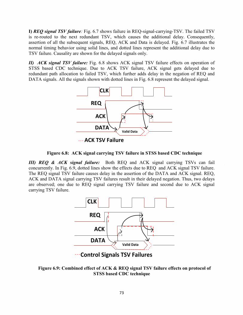
73
I) REQ signal TSV failure: Fig. 6.7 shows failure in REQ-signal-carrying-TSV. The failed TSV
is re-routed to the next redundant TSV, which causes the additional delay. Consequently,
assertion of all the subsequent signals, REQ, ACK and Data is delayed. Fig. 6.7 illustrates the
normal timing behavior using solid lines, and dotted lines represent the additional delay due to
TSV failure. Causality are shown for the delayed signals only.
II) ACK signal TSV failure: Fig. 6.8 shows ACK signal TSV failure effects on operation of
STSS based CDC technique. Due to ACK TSV failure, ACK signal gets delayed due to
redundant path allocation to failed TSV, which further adds delay in the negation of REQ and
DATA signals. All the signals shown with dotted lines in Fig. 6.8 represent the delayed signal.
REQ
ACK
ACK TSV Failure
CLK
DATAValid Data
Figure 6.8: ACK signal carrying TSV failure in STSS based CDC technique
III) REQ & ACK signal failure: Both REQ and ACK signal carrying TSVs can fail
concurrently. In Fig. 6.9, dotted lines show the effects due to REQ and ACK signal TSV failure.
The REQ signal TSV failure causes delay in the assertion of the DATA and ACK signal. REQ,
ACK and DATA signal carrying TSV failures result in their delayed negation. Thus, two delays
are observed; one due to REQ signal carrying TSV failure and second due to ACK signal
carrying TSV failure.
REQ
ACK
DATA
Control Signals TSV Failures
CLK
Valid Data
Figure 6.9: Combined effect of ACK & REQ signal TSV failure effects on protocol of
STSS based CDC technique
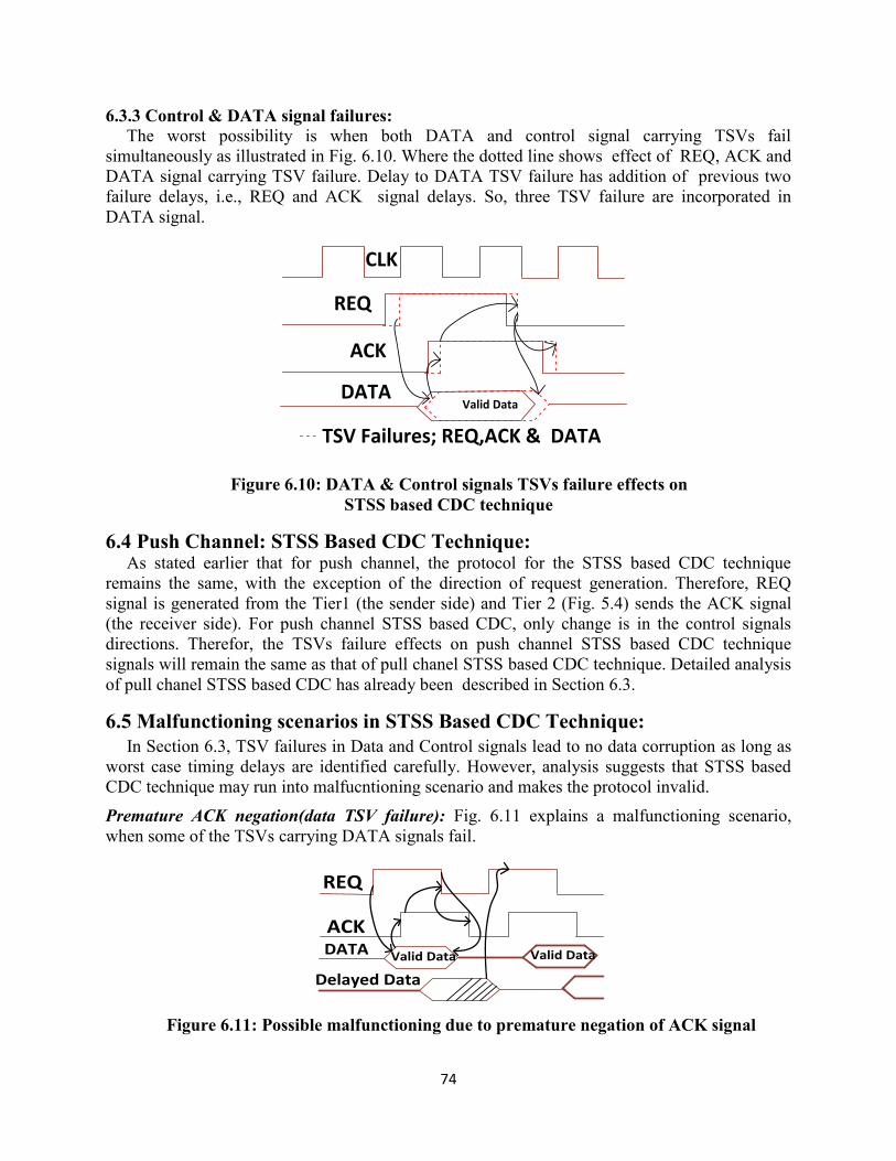
74
6.3.3 Control & DATA signal failures:
The worst possibility is when both DATA and control signal carrying TSVs fail
simultaneously as illustrated in Fig. 6.10. Where the dotted line shows effect of REQ, ACK and
DATA signal carrying TSV failure. Delay to DATA TSV failure has addition of previous two
failure delays, i.e., REQ and ACK signal delays. So, three TSV failure are incorporated in
DATA signal.
REQ
ACK
DATA
TSV Failures; REQ,ACK & DATA
CLK
Valid Data
Figure 6.10: DATA & Control signals TSVs failure effects on
STSS based CDC technique
6.4 Push Channel: STSS Based CDC Technique: As stated earlier that for push channel, the protocol for the STSS based CDC technique
remains the same, with the exception of the direction of request generation. Therefore, REQ
signal is generated from the Tier1 (the sender side) and Tier 2 (Fig. 5.4) sends the ACK signal
(the receiver side). For push channel STSS based CDC, only change is in the control signals
directions. Therefor, the TSVs failure effects on push channel STSS based CDC technique
signals will remain the same as that of pull chanel STSS based CDC technique. Detailed analysis
of pull chanel STSS based CDC has already been described in Section 6.3.
6.5 Malfunctioning scenarios in STSS Based CDC Technique:
In Section 6.3, TSV failures in Data and Control signals lead to no data corruption as long as
worst case timing delays are identified carefully. However, analysis suggests that STSS based
CDC technique may run into malfucntioning scenario and makes the protocol invalid.
Premature ACK negation(data TSV failure): Fig. 6.11 explains a malfunctioning scenario,
when some of the TSVs carrying DATA signals fail.
REQ
ACKDATA Valid Data
Delayed Data
Valid Data
Figure 6.11: Possible malfunctioning due to premature negation of ACK signal

75
Specific DATA lines corresponding to the failed TSV are delayed but if no proper mechanism
is applied to check the completeness of data, the ACK signal may negate prematurely. This is
because ACK signal is negated as soon as the REQ signal is negated. Consequently, due to
premature negation of the ACK signal, the delayed DATA gets corrupted, which is elaborated in
shaded region in Fig. 6.11. Data is being transferred serially.
In Fig. 6.11, it is shown that the data from previous transaction is not negated (shaded
portion), while REQ is asserted for next data transaction. Hence, the receiver may erroneously
considers the existing data on data lines as data for next data transaction. Therefore, some sort of
mechanism is required to indicate completeness of the data transaction.
6.6 Timing Analysis of STSS based CDC technique:
As we illustrated for the case of QDI based GALS CDC, in this section we are elaborating timing analysis for STSS based CDC technique. It is shown in Fig. 5.4 that the REQ, ACK and DATA signals are transferred through TSVs for STSS based CDC technique. For the data transaction, it has also been assumed that incoming data of different clock domains is synchronized with the help of STSS interface (Tier 1, Fig. 5.4). Data is written in FIFO (Fig. 5.4) and receiver can request/read the data at any instant of time. Once data transaction completes, both the REQ and ACK signals are negated from their respective sides. Any delay in the data transaction sequence causes the delay in interface operation. Timing constraints of the data transfer path in STSS based CDC technique (Fig. 5.4) are illustrated in (6.6), which assumes a pull channel:
TTRANSFER = TREQ-to-DATA + TDATA-to-ACK + TACK-to-REQ
+ max (TREQ-to-ACK,TREQ-to-DATA) (6.6)
In Eq. (6.6), TTRANSFER shows the time required for one complete data transaction as seen by the receiver, from the time receiver sees the assertion of REQ signal to the final negation of DATA signal. TREQ-to-DATA represents the time duration, that receiver (Fig. 5.4) sees once it initiates the REQ signal and gets back the asserted DATA signal. TDATA-to-ACK is duration observed at the receiver, from DATA signal assertion to ACK signal assertion. The third term TACK-to-REQ, represents time duration seen at the receiver side (Fig. 5.4), from assertion of the ACK signal to the negation of REQ signal. TREQ-to-ACK and TREQ-to-DATA shows time duration measured at the receiver end from negation of the REQ signal to the ACK and DATA signals negation, respectively. For the worst case analysis, maximum time duration from the negation of REQ signal to the ACK and DATA signals negation is taken into consideration.
Delay in data transaction can be represented with Eq. (6.7). TTRANSFER-JOINT represents new timing constraint for one data transaction, in case of failures in REQ, ACK and DATA carrying TSVs.
TTRANSFER-JOINT = TREQ-to-DATA+TDELAY1 + TDATA-to-ACK + TDELAY2+ TACK-to-REQ + max (TREQ-to-ACK,TREQ-to-DATA) +TDELAY (6.7)
In Eq. (6.7) TDELAY, TDELAY1 and TDELAY2 represent delays introduced due to the failure in
TSVs carrying REQ, DATA and ACK signals respectively. All three cases have been
highlighted in Fig.6.6 to Fig.6.10.
First, delay added due to the TSVs failure should be minimized. To minimize the delay,
efficient redundant TSV allocation techniques can be chosen at design stage of the interface.

76
Timing constraint mentioned in Eq. 6.8, should be fulfilled while utilizing a particular redundant
TSV technique.
TWIDTH >TDELAY (6.8)
In Eq. 6.8, TWIDTH represents the time duration for the one data bit. For example, X bits are in
one data burst and that specific burst is of the time duration T. Then, TWIDTH can be calculated by
X/T. TDELAY is path re-routing time in case TSV fails. Eq. 6.8 would help in optimizing the
delay to prevent data being corrupted.
Secondly, in the protocol a data completion signal needs to be added. The next data request
can be generated until the data completion signal is received. Inclusion of both constraints i.e.,
data completion signal in protocol and Eq. (6.8) timing constraint, would make design free from
the any chances of the data corruption.
Thirdly, another mechanism can be devised to avoid the malfunctioning. If data signal
carrying TSVs fail, this failure can be feedback to the REQ signal to negate the REQ signal with
some delay equal to TSV re-routing time. In case, the ACK signal TSV fails, it can be feedback
to delay data signal with time equal to the TSV re-routing. Addition of two feedbacks, one to the
REQ signal in case data signal TSVs fail and other feedback to the data signals for the ACK
signal carrying TSV failure, can avoid malfunctioning.

77
CHAPTER 7
CLOCK DOMAIN CROSSING IN 3-D IC (SIMULATIONS)
In order to verify our analysis electrical simulation were performed using IHP microelectronics
90nm libraries in Cadence. Both of the CDC techniques, i.e., the QDI based GALS interface and
STSS interface were simulated. For QDI based GALS CDC technique we used GAsP
asynchronous interface [63] as switching mechanism for simulation purposes. We obtained a
maximum operational frequency of about 1.2GHz while on the other hand, it was found that
STSS interface circuit, operates at frequency of 500MHz technique due to the limitations in
synchronization delay.
For simulation purposes, the electrical model of TSV is used, as explained in the Chapter 2 and
used across different tiers of Fig. 5.1 &5.4 to do the inter-tier communications. TSV modeled
[49] by using analytical method. TSV parasitic values depend on various geometrical factors
such as length, diameter, and metal characteristics of TSV. In our case, we assumed, in
accordance with the guidelines of ITRS 2013, a TSV of 6um in diameter, 20um in length, oxide
thickness of 120nm and 10um pitch distance. Using the state of the art empirical analysis based
model from reference [49] following parasitic values (RLC) are obtained R=12.89mΩ, C=9.807
fF and L=5.816pH respectively.
Fig. 7.1 provides the simulation results of QDI based GALS interface (Fig. 5.1), according to
the delay insensitive protocol as detailed in the Chapter 5.
Figure 7.1: Simulation of QDI based GALS CDC in 3-D ICs

78
Simulation waveforms shown in Fig. 7.1, for the case of no failures in the TSVs of data and
control signals. It shows an overall time of 750 ps for the one data transaction and power
consumption of 2.75 mW with energy of 14.17mJ for the four bit data transaction as mentioned
in first row of Table 7.1. While, second row of Table 7.1 shows the performance parameters for
the STSS interface.
In terms of basic three parameters, power, energy and delay for both CDC techniques, it shows
that there is very little difference between the two CDC techniques. But if energy-delay product
is calculated, the QDI based GALS interface is marginally better.
Table 7.1: Measurements of three basic parameters of CDC techniques
in 3-D ICs for 4-bit data transaction
S.
No
CDC
Technique
Power
(mW)
Energy
(mJ)
Delay
(ns)
Energy
Delay
(pJs)
Power
Delay
(pWs)
1 QDI based
GALS
interface
2.75 14.17 .75 10.63 2.06
2 STSS
interface 2.78 10.51 1.03 10.83 2.86
As mentioned in the Chapter 6 TSV failures lead towards delay in the operation. These
failures include failure of data (RR) signal and control signals. Both the data and control signal
failures demonstrates worst case because of the double failures causing incremental delays.
Intentional failure are introduced in the TSVs carrying these two categories of signals (data and
control) to validate the claim in the Chapter 6 about the QDI based GALS interface. The
introduction of failures, re-routed TSVs to redundant TSVs (1:4 redundancy) and delay added in
each data transaction.
Fig. 7.2 shows simulation results of the QDI based GALS interface, for failures in the data
and control signals TSVs. The control signal TSV failure introduced a delay of 106 ps (Eq. 6.3),
validating our claim regarding the control signal failure. Whereas, the DATA (RR) carrying
TSVs failure added delay of about 153 ps (Eq 6.2). Both the ACK2 and DATA (RR) signal
carrying TSV failure at same time instant resulted in delay of 259 ps (Eq. 6.4) as mentioned in

79
Table 7.2. It also validates our worst case formalization about the TSVs failure, which causes
more delay but no malfunctioning.
The usage of TSV redundancies, such as 2:4 [73] and router based [74] TSV redundancies,
provides more TSV failure tolerance but at the cost of increased delay as compare to the 1:4 TSV
redundancy [72].
Figure 7.2: Simulation of QDI based GALS interface (Data & Control signal failure)
Control signal failure resulted in 106 ps and data signal in 153ps delay. Overall, 259ps delay
comes out as 259 as in Table 7.2.
Table 7.2: Timing overhead due to TSV failure
S.
No
CDC
Technique
Control
signal TSV
Failure (ps)
Data signal
TSV Failure
(ps)
Data & Control
signals
TSV Failure (ps)
1 QDI based
GALS 106 153 259
2 STSS
interface 19 15 34
As a first step towards the simulations of loosely synchronous CDC technique, the failure
zone of STSS [71] circuitry is calculated. Failure zone comes out about 70ps. Plugging in the
failure zone time and clock time period in Eq. (2.1), error probability of.035 or 3.5 % is

80
achieved. FIFO as described in [75] is added to simulate the 3-D environment for STSS based
loosely synchronous CDC (as shown in Fig. 5.4).
Fig. 7.3 illustrates simulation waveform of loosely synchronous CDC. Simulation results are
according to the protocol as described in Fig. 5.5. The time for one data transaction comes out
1.03ns as reported in Table 7.1.
Figure 7.3: Simulation of clock domain crossing using STSS interface in 3-D IC
Failures introduced in ACK, REQ and DATA signals TSVs to simulate, analyze and validate
the consequences as detailed in section 6.4 &6.5 of the Chapter 6. Fig. 7.4 is the simulation
waveform showing the results based on signals using redundant (1:4 redundancy) TSV paths.
This is the worst delay case simulation when both DATA and control signal fails.
Figure 7.4: STSS interface CDC technique in 3-D IC (Data & Control signal TSV failure)
Simulation of worst case, i.e., DATA and control signal carrying TSVs has been performed
using 1:4 TSV redundancy architecture [73]. Penalty due to failure of REQ signal is about 11ps
(Fig. 6.7), 8ps (Fig. 6.8) due to ACK signal, 19 ps (Fig. 6.9) for both REQ and ACK signals and
data signal TSV failure causes 15ps (Fig. 6.6) delay. Overall, timing penalty comes out 34ps
(Fig. 6.10) (Row 3, Table 7.2).Using redundant TSVs causes the delay as evident from Fig. 7.4,
but soemtime delay may add upto signaficant level or operation sequence may lead towards
malfunctioning in circuit operation as detailed in the Section 6.5 (Chapter 6).

81
Fig. 7.5 is the case when the ACK signal negated prematurely from the receiver side without
realizing that data is delayed and not received completely. It caused the malfunctioning in system
as DATA is not being received completely while the ACK and REQ signals terminated
(highlighted with the help of circle in Fig. 7.5). Hence, invalidating the protocol and lead to the
malfunctioning scenarios due to premature negation of control signal. This scenario is simulated
and illustrated in Fig. 7.5.
Figure 7.5: Malfunctioning scenario of STSS interface CDC in 3-D IC
Fig. 7.5, two data item sent but not received at the other end. So, only delay in operation is not
penalty, malfunctioning chances are also there in the STSS interface CDC technique.
In general area wise, the QDI based GALS interface design has advantage over the STSS
interface for lower number of bits, but as we increase the number of bits, the STSS interface
becomes more advantageous. For example if 1-bit is transferred the STSS interface uses 1.44
times more area compared to the QDI based GALS interface (Table 7.3), whereas, if 16 bit data
transaction is made concurrently, the QDI based GALS interface consumes about 1.14 times the
STSS interface. Delay wise, the QDI based GALS interface presents more delay in adoption of
redundant path as compared to the STSS interface as counterpart.
Table 7.3: Hardware overhead of CDC techniques
Case
CDC using STSS
interface QDI based GALS CDC
PMOS NMOS Total PMOS NMOS Total
1-bit 1.37X1 1.66Y1 1.44T1 X1 Y1 T1
4-bit 1.12X2 1.25Y2 1.16T2 X2 Y2 T2
8-bit X3 1.07Y3 T3 1.25X3 Y3 1.15T3
16-bit X4 Y4 T4 1.19X4 1.03Y4 1.14T4

82
Simulation of three TSV redundancy techniques, mentioned and analyzed in the Chapter 5, is performed using MATLAB 7.0. We analyzed the hardware overhead required for each redundancy technique upto 400 signals. Fig. 7.6 illustrates product of hardware with the number of cells used, using 1:4, 2:4 and router based TSV redundancy techniques.
In order to provide a fair comparison we normalized the product of number of cells and area overhead (called as hardware overhead) for 5x5 router based redundancy technique over 400 signals.
Fig. 7.6 shows that as expected with increment in number of signals hardware overhead will increase. However, effective redundancy per cell is reduced with increment in the number of signals. It can be seen effective redundancy of router based TSVs are better at the expense of added hardware.
Figure 7.6. Hardware overhead X cells required (on left y-axis) and effective number of redundant TSVs (on right y-axis) for different number of signals
Nonetheless, For 250 signals, the hardware overhead for 3x3 router based technique is about 3 times more than 1:4 redundancy technique, while providing 5 times more effective redundancy per cell. Hence, if the foundry data is available with respect to yield percentage of TSVs, this study will help the designer to choose the right redundancy technique under a given condition.

83
CHAPTER 8
CONCLUSION & FUTURE WORK
8.1 Conclusion:
The first major objective achieved in this work is to successfully prove that the QDI based GALS
asynchronous interfaces can be utilized efficiently in the GALS design. Secondly, we have
characterized the different interfaces based on complexity and performance so that a designer
may make an informed decision on choosing a particular interface. Table 4.1 shows that for any
number of bits of data transaction, the modified RSDL interface outperforms other interfaces
with an improvement of at least 22% in latency. In terms of power, the encoding and decoding
techniques of the modified GAsP and STFB based GALS systems have to be efficient, to
compete with the modified RSDL. The approach developed in this work also provides a flexible
interfacing mechanism for the MPSoC based ASIP. Our technique can be combined with the
configurable platform technique [27] to automate the generation of interfaces in the platform.
Moreover, the proposed interfaces can be incorporated as external/internal communicating
modules in configurable platform technique. It will help in reducing time-to-market as the
overall design process accelerates with the proposed design template, in conjunction with
configurable platform technique with minimal changes.
The QDI based GALS design templates are introduced, to leverage from the robust QDI based
GALS asynchronous interface. Two different templates are proposed and analyzed with three
different asynchronous interfaces, utilizing the RTZ and ST signaling schemes. Robustness of
the proposed design templates is observed using corner cases. Our template based approach
reduces the design complexity of the IP based GALS design and the results provided on several
metrics allow designers to make an informed decision to choose the GALS interface that fits best
to the design need. Compared to the state of the art GALS based designs, our templates offer
much flexibility in terms of the frequency variations and phase difference between the
communicating modules.
3-D IC is an emerging technology which can be leveraged further by use of the GALS
templates. Due to multi storey structure, each tier can have an IP, independent of other tiers. This
leads us to the use of clock domain crossing CDC in 3-D ICs. For CDC, the QDI based GALS

84
systems can be proven very beneficial. There is a special scenario that can arise; it is the
existence of out of phase frequencies at multiple tiers. So, the modified STSS based interface
was utilized for such scenarios.
Incorporation of two CDC techniques in 3-D IC has been presented in this work. Guidelines
are provided for placement of different components at different logic layers of 3-D IC with
justification of data signals, control signals and TSVs requirements. This incorporation suggests
that how CDC techniques are suitable and adaptable in 3-D environment. The QDI based GALS
asynchronous interface requires a local clock on each layer regardless of communicating
frequencies, whereas the STSS interface is more suitable with global clock distribution network.
Various TSV redundancies techniques used to tolerate the TSV failure while data transportation.
Each redundancy technique has its own specialized features like fault tolerance and overhead.
Detailed timing characterization of the TSV failures for both CDC techniques provided based
upon asynchronous channels analysis i.e., push and pull channel. The timing characterization is
done on the basis of the TSV failures carrying data and control signals. Effects of each failure
scenario on protocol elaborated through waveforms and mathematical equations. These cases
validated through the simulation results. The QDI based GALS asynchronous interface resulted
in more timing overhead, but no erroneous operation due to its delay insensitivity nature. On the
other side, the loosely synchronous STSS interface came up with low timing overhead in failure
case, but it has possibility of malfunctioning. In no failure, performance wise both techniques are
same based upon the energy delay product calculation.
In general, the QDI based GALS templates uses more hardware and area, but less power
consumption. The energy and power delay product of both the QDI based GALS template and
STSS shows that STSS interface is efficient based upon these parameters. In performance, the
QDI based GALS template can be slower as it involves the ACK2 (acknowledgement) signal
which is controlled by the data signals. But this template has an edge of less probability of
malfunctioning as data may be delayed. So, its operation completion can be delayed but it cannot
erroneous due to no separate control involvement. Means timing assumption of data arrival is
excluded. On the other hand control signal handling of modified STSS based interface is a bit
faster as it is based upon internal clock switching which is faster, but it needs timing assumption

85
of the data. That may malfunction on data delay. A complete analysis on timing assumption is
provided in the Chapter 6.
Operational frequency of both the CDC techniques, i.e., the QDI based GALS and STSS
based CDC can be same. But there is a problem in case of the modified STSS interface, as
frequency of clock goes higher probability of failure also increases. Mathematically, failure
probability is failure zone duration divided by clock period. Failure zone determination
procedure has been explained in the Chapter 5. Failure zone will remain same for a d-flip flop, in
our case it is 60ps, so clock period reduction results in higher failure probability.
No separate global clock distribution network is required in the QDI based GALS template
because of the local clock generation. It provides various benefits in terms of IP reuse and less
consumption of silicon area. On the other way round, synchronization technique is free from
local clock generation at every stage which free the designer from redesign of clock distribution
but it requires more silicon area.
8.2 Future Work:
As future work, generation of local clock for QDI based GALS system can be more optimized
by introducing a proper clock distribution logic on each of the sender and receiver end. Encoding
and decoding of each DI code can be incorporated, which will provide a complete picture of
overall system. In such a system where a separate operational logic designs on each end, will
provide to investigate system more clearly and carefully. Another possible future contribution
could be layout level implementation to provide more realistic and much close to fabrication
level results.
We have utilized the RTZ signaling scheme (all data signals should be at logic zero when no
bit is being transmitted), however the NRTZ (non-return to zero) scheme can also be used which
requires half bandwidth as compared to the RTZ, but NRTZ scheme adds the hardware
complexity. There are so many other DI codes available that can be used to encode the data bits,
to transfer them to another clock domain. The main focus while choosing DI codes should be
simplicity in the implementation, the less timing overhead, the minimum hardware and the lower
power consumption. Such codes should be used that can be transmitted and perceived without
any error.

86
As far incorporation of CDC in 3-D ICs is concerned, only TSV requirement factor is
analyzed and verified in deep. TSVs can be further analyzed in terms of silicon area footprint
along the relevant parasitic factors. Temperature reduction mechanism and power distribution
network can be designed more carefully. Testing is another factor that can be done to verify 3-D
IC functionality at fabrication level. Overall 3-D system can be improved by introducing various
logic designs at the separate tiers with the introduction of local or global network along factors
mentioned above.
TSV is main source of communication across different tiers in 3-D IC. In the number of TSV
required, apparently it seems that the STSS based interface is much better but in reality it is not
so, there are other attributes which can be considered. Every scenario has its own preferences
that is why guidelines are provided so that a particular selection can be made. TSV failure
always requires the signal shifts which introduce delays. Many redundancy techniques can be
adopted but each has a maximum failure tolerance. For example, 1:4 technique [72] can bear one
while 2:4 [73] technique can bear two failures at maximum. Although two failures can be
handled with 2:4 approach but it has two times delay associated with it in case of the failure as
compare to 1:4 redundancy technique. Similarly router based redundancy approach provides a
novel mechanism for back up path adaptation but at expense of more hardware and increased
delay.
TSV requirement according to different data encodings shows that m-of-n encoding is much
better than the other two in encodings in QDI based GALS. But encoding and decoding has also
some cost which is more for the m-of-n codes. Encoding and decoding is easier for the 1-of-N
signaling scheme in hardware requirement and in power consumption. The dual rail encoding is
also efficient but it has disadvantage of requirement of asynchronous interface for each data bit
encoding. The NRTZ signaling scheme can also be used where bandwidth is a critical factor
instead of the RTZ but it will be at cost of more hardware and intensive level detective
mechanism.

87
Bibliography
[1] Amde, M. Felicijan, T. ; Efthymiou, A. ; Edwards, D. ; Lavagno, L., “Asynchronous On-
Chip Networks”, In Proc. Of IEE transaction on Computers and Digital techniques,
(Volume: 152, Issue:2), March 2005, pp. 273-283.
[2] “Principles Of Asynchronous Circuit Design”, A Systems Perspective, Edited by Jen
Sparso Technical University of Denmark and Steve Furbur The University of Manchester
UK, published by Kluwer Academic Publishers Boston/Dordrecht/London
[3] Rosenfeld, J., Friedman, E.G., “Design Methodology for Global Resonant H-Tree Clock
Distribution Networks”, In Proc. Of IEEE transaction on Very Large Scale Integration
(VLSI) Systems (Volume: 15 , Issue: 2), Feb 2007, pp.135-148.
[4] “Digital Integrated Circuits (2nd Edition)”, A design perspective, BY Jan M. Rabaey &
Anantha Chandrakasan & Borivoje Nikolic.
[5] Semiconductor Industry Association, “International technology roadmap for
semiconductors (ITRS)”, 2011.
[6] D. Chapiro, “Globally Asynchronous Locally Synchronous Systems”, Ph.D. thesis,
Stanford University, October 1984.
[7] Z. Yu and B. M. Baas, “High Performance, Energy Efficiency, and Scalability With
GALS Chip Multiprocessors”, In Proc. of IEEE transaction on Very Large Scale
Integration (VLSI) systems, (Volume: 17, Issue: 1), January 2009, pp. 66-79.
[8] K. S. Chong, K. L. Chang, Bah-H. Gwee and J. S. Chang, “Synchronous-Logic and
Globally-Asynchronous-Locally-Synchronous (GALS) Acoustic Digital Signal
Processors”, In IEEE journal of solid state circuits, (Volume: 47, Issue:3) , March 2012,
pp.769-780.
[9] Mack, C.A. “Fifty Years of Moore's Law”, In Proc. Of IEEE Transaction on
Semiconductor Manufacturing, (Volume:24 , Issue: 2 ), May 2011, pp. 202-207.
[10] K.C Saraswat, “3-D ICs: Motivation, performance analysis, technology and
applications”, In 17th IEEE International symposium on Physical and Failure
Analysis of Integrated Circuits (IPFA), IEEE, Singapore, July 2010, pp.1-6.
[11] Pavlidis, V. F. De Micheli, G. “Skew variability in 3-D ICs with multiple clock
domains”, IEEE International Symposium on Circuits and Systems (ISCAS), IEEE,
MAY 2011, pp. 2221 – 2224.
[12] P. Teehan, M. Greenstreet, and G. Lemieux, “A Survey and Taxonomy of GALS
Design Styles”, IEEE transactions on Design & Test of Computers (Volume: 24 , Issue:
5 ), Sept.-Oct. 2007, pp. 418 – 428.
[13] M. Fenghao, and C. Svensson, “Self-Tested Self-Synchronization Circuit for
Mesochronous Clocking”, IEEE Transactions on Circuits and Systems II: Analog and
Digital Signal Processing (Volume: 48, Issue: 2), IEEE, February 2001, pp. 129 – 140.

88
[14] J. Muttersbach, T. Villiger and W. Fichtner, “Practical Design of Globally-
Asynchronous Locally-Synchronous systems”, In Proc. of International Symposium on
Advanced Research in Asynchronous Circuits and Systems (ASYNC‘00), Eilat, IEEE,
April 2000, pp. 52-59.
[15] K. Y. Yun and R. P. Donohue, “Pausible clocking: A First step towards
heterogeneous systems”, In Proc. of International Conference on Computer Design
(ICCD‘96), Austin TX, IEEE, October 1996, pp.118-123.
[16] Mark De Clercq and Radu Negulescu, “1.1-GDI/s Transmission between Pausible
Clock Domains”, In Proc. of IEEE International Symposium on Circuits and Systems
(ISCAS‘02), Vol: 2, Phoenix-Scottsdale AZ, IEEE, May 2002, pp.768-771.
[17] S. Moore, G. Taylor, R. Williams and P. Robinson, “Point to Point GALS
Interconnect”, In Proc. of International Symposium on Asynchronous Circuits and
Systems (ASYNC‘02), IEEE, April 2002, pp. 69-75.
[18] S. Dasgupta and A. Yakovlev, “Comparative analysis of GALS clocking
schemes”, In IET Journal of Computers & Digital Techniques, (Volume: 1, Issue: 2),
March 2007, pp.59-69.
[19] R. Mullins and S. Moore, “Demystifying Data-Driven and Pausible Clocking
Schemes”, In Proc. of IEEE International Symposium on Asynchronous Circuits and
Systems (ASYNC‘07), Berkeley CA, IEEE, March 2007, pp.175-185.
[20] P. Teehan, M. Greenstreet and G. Lemieux, “A Survey and Taxonomy of GALS
Design Styles”, In Proc. of IEEE Design & Test of Computers, (Volume: 24, Issue: 5),
IEEE, Sept-Oct. 2007, pp.418-428.
[21] Hasan, Syed Rafay, Normand Bélanger, Yvon Savaria, and M. Omair Ahmad.
"All digital skew tolerant synchronous interfacing methods for high-performance point-
to-point communications in deep sub-micron SoCs", In the journal of IEEE VLSI,
(Volume:44, Issue:1), 2011, pp.22-38.
[22] Hasan, Syed Rafay. "Inter-module Interfacing techniques for SoCs with multiple
clock domains to address challenges in modern deep sub-micron technologies." PhD
thesis dissertion, Concordia University, 2009. Available online at:
http://spectrum.library.concordia.ca/976728/1/NR67368.pdf
[23] P. Teehan, Greenstreet, M. ; Lemieux, G.”A survey and Taxonomy of GALS
design styles”, In Proc. Of IEEE transaction on Design and Test of Computers, (Volume:
24, Issue: 05), Sept.-Oct 2007, pp. 418-428.
[24] Yun, K.Y. , Dooply, A.E, “Pausible clocking-based heterogeneous systems”, In
Proc. Of IEEE transaction on Very Large Scale Integration (VLSI) Systems, (Volume: 7
, Issue: 4 ), Dec 1999, pp.482-488.
[25] Rahimian, M.A. , Mohammadi, S., Fattah, M.,” A high-throughput, metastability-
free GALS channel based on pausible clock method”, In Proc of IEEE 2nd Asia
Symposium on Quality Electronic Design (ASQED), Aug.2010, pp. 294-300.

89
[26] Monthie, J. , Sreekumar, V. ; Yashwante, R., “Impact of Power Supply Noise on
Clock Jitter in High-Speed DDR Memory Interfaces”, In Proc. Of IEEE 26th
International Conference on VLSI Design and12th International Conference on
Embedded Systems (VLSID), Jan. 2013, pp. 262-266.
[27] Xiao, Yong , Zhou, Runde, “Low latency high throughout circular asynchronous
FIFO”, In Proc. Of IEEE transaction on Tsinghua Science and Technology (Volume:13
, Issue: 6 ), Dec. 2008, pp.812-816
[28] Mˇ Krstic´, E Grass, P Vivet & F K Gu¨rkaynak “Globally Asynchronous,
Locally SynchronousCircuits: Overview and Outlook”, In Proc. Of IEEE transactions on
Design and Test of Computers, (Volume: 24, Issue: 05), Sept.-Oct 2007, pp. 430-441.
[29] J Mekie, S C Dinesh, K. Sharma, “Evaluation of pausible clocking for interfacing
high speed IP cores in GALS Framework”, In Proc. of IEEE 17th International
Conference on VLSI Design, 2004, pp.559-564.
[30] A Upadhyay, S R Hasan, M Nekili, “A Novel Asynchronous Wrapper using 1-
of4 Data Encoding and Single-Track Handshaking”, In Proc. Of IEEE 2nd
Annual
Northeast Workshop on Circuit and Systems, NEWCAS , June 2004, pp.205-208.
[31] F. Gu¨rkaynak , Oetiker, S. ; Kaeslin, H. ; Felber, N. ; Fichtner, Wolfgang;
“GALS at ETH Zurich: Success or Failure?” , In Proc. Of 12th IEEE International
Symposium on Asynchronous Circuits and Systems (ASYNC 06), IEEE CS Press, 2006,
pp. 150-159.
[32] D. Lattard , Beigne, E. ; Bernard, C. ; Bour, C. “A Telecom Baseband Circuit
Based on an Asynchronous Network-on-Chip”, In Proc. Of IEEE International
Conference on Solid- State Circuits (ISSCC 07), IEEE, 2007, pp. 258-601.
[33] Krstic, M., Grass, E., “BIST Technique for GALS System”, In Proc. Of IEEE 8th
Euromicro Conference on Digital Systems and Design, Aug.-Sept 2005, pp.10-16.
[34] Mˇ Krstic´, E Grass, P Vivet & F K Gu¨rkaynak “Globally Asynchronous,
Locally SynchronousCircuits: Overview and Outlook”, In Proc. Of IEEE transaction on
Design and Test of Computers, (Volume: 24, Issue: 05), Sept.-Oct. 2007, pp-430-441.
[35] K S Chong, K L Chang, B H Gwee, J S Chang, “Synchronous-Logic and
Globally-Asynchronous-Locally-Synchronous (GALS) Acoustic Digital Signal
Processors”, In IEEE Journal Of Solid-State Circuits, (Volume: 47, Issue: 3), MARCH
2012, pp.769-780.
[36] J M Chabloz, A Hemani, “Low-Latency No-Handshake GALS Interfaces for
Fast-Receiver Links”, In Proc. Of IEEE 25th International Conference on Very Large
Scale Integration (VLSI) Design, Jan.2012, pp.191-196.
[37] Rebaud, B., Belleville, M. , Bernard, C. , Wu, Z. Robert, M. ; Maurine,
P. ; Azemard, N., “Setup and Hold Timing Violations Induced by Process Variations, in a
Digital Multiplier”, In Proc. Of IEEE International Symposium on ISVLSI '08, April
2008, pp.316-321
90
[38] Moreira, M.T.Guazzelli, R.A. and Calazans N.L.V., “Return-to-one protocol for
reducing static power in C-elements of QDI circuits employing m-of-n codes”, In Proc.
of 25th Symposium on Integrated Circuits and Systems Design (SBCCI), Brasilia, IEEE,
Aug-Sept 2012, pp.1-6.
[39] Campobello, G. Castano, M. Ciofi, C.and Mangano, D. “GALS Networks on
Chip: A New Solution for Asynchronous Delay-Insensitive Links”, In Proc. of IEEE
Design, Automation and Test in Europe Conference and Exhibition (DATE), (Volume: 4)
Munich, IEEE, March 2006, pp.1-6.
[40] X. Fan1, M. Krstić1, E. Grass1, B. Sanders2, and C.Heer, “Exploring Pausible
Clocking Based GALS Design for 40-nm System Integration”, In Proc. of Design,
Automation & Test in Europe Conference & Exhibition (DATE), Dresden, IEEE, March
2012.
[41] J.M. Chabloz and A.Hemani,“Low-Latency Maximal-Throughput
Communication Interfaces for Rationally Related Clock Domains”, In Proc. of IEEE
transaction on Very Large Scale Integration (VLSI) systems, (Volume: 22, Issue: 3),
IEEE, April 2013, pp.641-654.
[42] A. J. Martin, and M. Nystrom,“Asynchronous techniques for system-on-chip
design”, In Proc. of the IEEE, (Volume: 94, Issue: 6), June 2006, pp.1089-1120.
[43] J. M. Chabloz and A. Hemani, “A GALS Network-on-Chip based on Rationally-
Related Frequencies”, In Proc. Of 29th
IEEE International Conference on Computer
Design (ICCD), Amherst MA, IEEE, October 2011, pp.12-18.
[44] Y.T. Chang, W.C. Chen, H.Yue, Tsai, W.M. Cheng, C.J. Chen and F.C. Cheng,
“A Low-latency GALS Interface Implementation”, In Proc. of IEEE Asia Pacific
Conference on Circuits and Systems (APCCAS), Kuala Lumpur, IEEE, December 2010,
pp.1183-1186.
[45] T. Verhoeff, “Delay-insensitive codes--an overview”, Computing Science Notes,
Department of Mathematics and Computing Science Eindhoven University of
Technology The Netherland , January 1987.
[46] Bainbridge, W.J., Toms, W.B. ; Edwards, D.A. ; Furber, S.B.,” Delay-insensitive,
point-to-point interconnect using m-of-n codes” In Proc. Of IEEE Ninth International
Symposium on Asynchronous Circuits and Systems, May 2003, pp.132-140.
[47] A.M.G. Peeters, “Single Rail Handshake Circuits”, PhD thesis, Eind Hoven
University of Technology, June 1996.
[48] Q. Xu, L. Jiang , H. Li , and B. Eklow, “ Yield Enhancement for 3D-Stacked ICs:
Recent Advances and Challenges”, In Proc. of IEEE 17th Asia and South Pacific Design
Automation Conference (ASP-DAC), Sydney NSW , Jan. 30-Feb. 2 2012, pp. 731 –
737.
[49] Katti, Guruprasad, M. Stucchi, K. De Meyer, and W. Dehaene. "Electrical
modeling and characterization of through silicon via for three-dimensional ICs", In Proc.
Of IEEE transaction on Electron Devices (Volume: 57, Issue: 1), Jan. 2010, pp. 256-262.

91
[50] Heegon Kim, Jonghyun Cho ; Myunghoi Kim ; Kiyeong Kim ; Junho
Lee ; Hyungdong Lee ; Kunwoo Park ;Kwang seong Choi ; Hyun-Cheol Bae ; Joungho
Kim ; Jiseong Kim,” Measurement and Analysis of a High-Speed TSV Channel”, In
Proc. Of IEEE transaction on Components, Packaging and Manufacturing Technology,
(Volume: 2 , Issue: 10 ), Oct. 2012, pp.1672-1685
[51] A. C. Hsieh, TingTing Hwang ; Ming-Tung Chang ; Min-Hsiu Tsai ; Chih-Mou
Tseng ; Hung-Chun Li, “TSV redundancy: Architecture and design issues in 3D IC”, In
Proc. of IEEE/ACM Design, Automation, and Test in Europe, IEEE, Dresden, 2010. pp.
166–171.
[52] Study of through silicon via induced transistor variations by Li Yu, B.E
Microelectronics, Thesis at the Tsinghua University (2009).
[53] Goplen, B., Sapatnekar, S.S.,” Placement of thermal vias in 3-D ICs using various
thermal objectives”, In Proc. Of IEEE transaction on Computer-Aided Design of
Integrated Circuits and Systems, (Volume: 25 , Issue: 4 ), April 2006. Pp. 692-709.
[54] Da-Cheng Juan, Garg, S. ; Marculescu, D., “Impact of manufacturing process
variations on performance and thermal characteristics of 3D ICs: Emerging challenges
and new solutions”, In Proc. Of IEEE International Symposium on Circuits and Systems
(ISCAS), May 2013, pp.541-544.
[55] Kung, D., Puri, R., “CAD challenges for 3D ICs”, In Proc. Of IEEE Asia and
South Pacific Design Automation Conference ASP-DAC 2009, Jan 2009, pp.421-422.
[56] Goel, S.K.,” Test challenges in designing complex 3D chips: What in on the
horizon for EDA industry?: Designer track”, In Proc. Of IEEE International Computer-
Aided Design (ICCAD), IEEE/ACM, San Jose CA, Nov 2012, pp.272.
[57] Hu Xu, Pavlidis, V.F. ; De Micheli, G.,” Skew variability in 3-D ICs with
multiple clock domains”, In Proc. Of IEEE International Symposium on Circuits and
Systems (ISCAS), May 2011, pp.2221-2224.
[58] Mallikarjun. P. Y, Dr. Y. S. Kumarswamy, “Analyzing 3D IC PDNs Using
Multiple Clock Domains to Obtain Worst-Case Power Supply Noise and Temperature
Variations”, In Proc. Of IEEE International Journal of Scientific & Engineering
Research, (Volume: 4, Issue: 12), December-2013, pp.1393-1399.
[59] S. Höppner, H. Eisenreich, S. Henker, D. Walter, G. Ellguth and R.Schüffny, “A
Compact Clock Generator for Heterogeneous GALS MPSoCs in 65-nm CMOS
Technology”, In Proc. of IEEE transaction on Very Large Scale Integration (VLSI)
systems, (Volume: 21, Issue: 3), March 2013, pp.566-570.
[60] X. Fan, M. Krstic and E. Grass, “Performance Analysis of GALS Data link Based
on Pausible Clocking”, In Proc. of 18th IEEE International Symposium on Asynchronous
Circuits and Systems (ASYNC), Lyngby , IEEE, May 2012, pp.126-133.
[61] Q. Yang, T. Wang, X. Su, L. Wang and X. Wang, “GALS Architecture of H.264
Video Encoding System on DN-DualV6-PCIe-4 FPGA Platform”, In Proc. of IEEE 11th

92
International Conference on Signal Processing (ICSP), Beijing, IEEE, October 2012,
pp.444-447.
[62] D. Ayachi, Y. Savaria, C. Thibeault, “A configurable platform for MPSoCs based
on application specific instruction set processors”, In Proc. of 7th
IEEE North-East
Workshop on Circuit and Systems (NEWCAS-TAISA‘09), Toulouse, IEEE, June-July
2009, pp.1-4.
[63] I. Sutherland, S. Fairbanks, “GAsP: a minimal FIFO control”, In Proc. of
7th
International Symposium on Asynchronous Circuits and Systems (ASYNC‘01), Salt
Lake City UT, IEEE, March 2001, pp.46-53.
[64] M. Ferretti, P.A. Beerel, “Single-track asynchronous pipeline templates using 1-
of-N encoding”, In Proc. of Design Automation and Test in Europe Conference and
Exhibition, (DATE‘02), IEEE, 2002, pp.1008-1015.
[65] N. Saadallah, Kong Xiaohua, R. Negulescu, “High-speed reduced stack dual lock
circuits”, In Proc. Of IEEE 10th
International Symposium on Asynchronous Circuits and
Systems, (ASYNC‘ 04), 2004, pp.219-228.
[66] A Agiwaland, M Singh, “An Architecture and a Wrapper Synthesis Approach for
Multi-Clock Latency-Insensitive Systems”, In Proc. of IEEE/ACM International
Conference on Computer-Aided Design, IEEE, November 2005, pp.1006-1013.
[67] X. Guan, D. Zhou, Y. Yang, Z. Zhu, “A GALS Delay-insensitive Self-timed
Wrapper for Network on Chips”, In Proc. Of IEEE Pacific Asia Conference on Circuits,
Communications and System, Chengdu, IEEE, May2009, pp.265-268.
[68] M.Santhi, S. Tungala, C. Balakrishna and G. Lakshminarayanan, “Asynchronous
Pipelined MB-OFDM UWB Transceiver on FPGA”, In Proc. Of IEEE Conference on
TENCON, Singapore, IEEE, January 2009, pp.1-5.
[69] J. D. Garcia-lasheras, “Efficient implementation of GALS systems over
commercial synchronous FPGA:A new approach”, From Electrical and Electronic
Engineering Dept, Public University of Navarre.
[70] P. Teehan, M. Greenstreet, and G. Lemieux, “A Survey and Taxonomy of GALS
Design Styles”, IEEE transactions on Design & Test of Computers (Volume: 24 , Issue:
5), IEEE, Sept.-Oct. 2007, pp. 418 – 428.
[71] M. Fenghao, and C. Svensson, “Self-Tested Self-Synchronization Circuit for
Mesochronous Clocking”, IEEE Transactions on Circuits and Systems II: Analog and
Digital Signal Processing (Volume: 48, Issue: 2), IEEE, February 2001, pp. 129 – 140.
[72] A. C. Hsieh, TingTing Hwang ; Ming-Tung Chang ; Min-Hsiu Tsai ; Chih-Mou
Tseng ; Hung-Chun Li “TSV redundancy: Architecture and design issues in 3D IC”, In
Proc. of IEEE/ACM Design, Automation, and Test in Europe (DATE), IEEE, Dresden,
2010. pp. 166–171.
[73] U. Kang, et al., “8 Gb 3-D DDR3 DRAM using through silicon-via technology”,
In IEEE Journal of Solid-State Circuits (Volume: 45, Issue: 1), IEEE, 2010, pp. 111–119.

93
[74] L. Jiang, Q. Xu, and B. Eklow, “On effective TSV repair for 3D-stacked ICs”, In
Proc. of IEEE/ACM Design, Automation, and Test in Europe, IEEE, Dresden, March
2012, pp.793-798.
[75] X. Wang, J. Nurmi, “A RTL Asynchronous FIFO design Using Modified Micro
pipeline”, In Proc. Of IEEE International Baltic Electronics Conference, IEEE, Tallin,
Oct. 2006, pp.1-4.