Global 450mm Consortium at CNSE - SEMI.ORG Minatech 042412.pdf · Global 450mm Consortium at CNSE -...
16
Michael Liehr, General Manager G450C, Vice President for Research Global 450mm Consortium at CNSE - CNSE Overview - G450C Vision - G450C Mission - Org Structure - Scope - Timeline
Transcript of Global 450mm Consortium at CNSE - SEMI.ORG Minatech 042412.pdf · Global 450mm Consortium at CNSE -...

G450C
Michael Liehr, General Manager G450C, Vice President for Research
Global 450mm Consortium at CNSE
- CNSE Overview- G450C Vision- G450C Mission- Org Structure- Scope- Timeline

G450CThe Road Ahead for Nano-Fabrication Technology
Anal./Digit.Conversion
Integrated Passives HV Power Sensors
ActuatorsBiochipsfluidics
More than Moore: Diversification
Mor
e M
oore
: Min
iatu
rizat
ion
130nm
90nm
65nm
45nm
32nm
22nm
Bas
elin
e C
MO
S: C
PU, M
emor
y, L
ogic
Information Processing
Digital contentSystem-on-chip
(SoC)
Interacting with people and environment
Non-digital content System-in-package
(SiP)
Combining SoC and SiP: Higher Value Systems
Optoelec. IntegrationWireless
Source: 2005 ITRS, Sematech, ITPC 2011
Fewer will sit in the Front of the “Scaling” Bus…
Leading-Edge Designs drive High Cost and High Volume
Sources: International Business Strategies; GLOBALFOUNDRIES
Heterogeneous Integration using 3D Technology
Hugh Demand in Smart Devices drives Utilization of “Older” Nodes

G450C
3
Fewer public and private playgrounds for:
• Developing new materials, processes and equipment
• Developing technology integration
• Optimizing manufacturing including resource conservation
Industry consolidation will continue as all 450mm participants exploit leading-edge technologies, therefore wafer size and scaling challenges will be hard to discern
“Bigger, yet smaller and more precise”
Cost and financial pressures create need for further pre-competitive collaboration
With permission: D.Armbrust, Sematech, R.Bruck, Intel, ITPC 2011

G450C• Full complement of state-of-the-art 300mm tools.• Used for 1xnm node development.• Compatible with previous generations. • Capacity of ~30 integrated wafer starts per day. • 24/7 operation.• Staffed with professional engineering and faculty.
College of Nanoscale Science and Engineering

G450CAnnouncement on September 27, 2011
• 2,500 new high-tech jobs, including: • 800 at the CNSE• 400 in Utica• 1,500 construction jobs in Albany
• $4.8 billion investment, most of it private • $400 million coming from NYS• R&D in Albany, Canandaigua, Utica,
East Fishkill and Yorktown Heights. • Intel intends to establish its East Coast
headquarters in Albany to manage 450mm development.
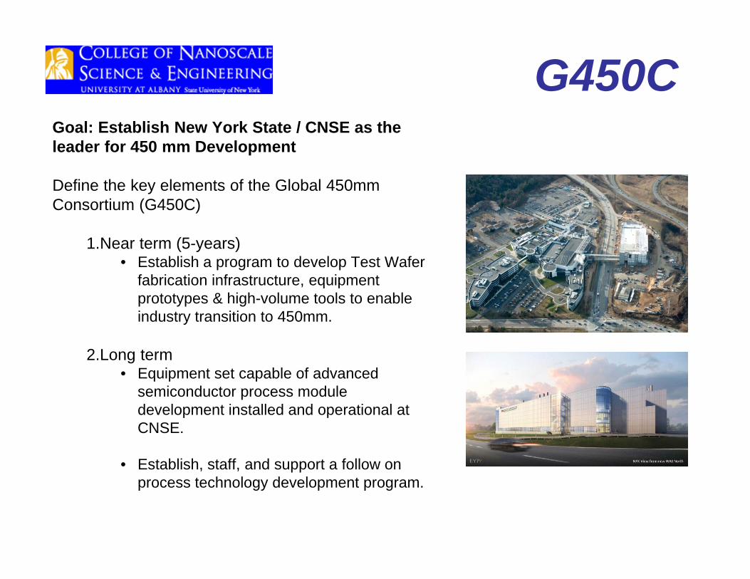
G450CGoal: Establish New York State / CNSE as the leader for 450 mm Development
Define the key elements of the Global 450mm Consortium (G450C)
1.Near term (5-years)• Establish a program to develop Test Wafer
fabrication infrastructure, equipment prototypes & high-volume tools to enable industry transition to 450mm.
2.Long term• Equipment set capable of advanced
semiconductor process module development installed and operational at CNSE.
• Establish, staff, and support a follow on process technology development program.

G450C
A public-private partnership program to develop a cost-effective test wafer fabrication infrastructure, equipment prototypes & high-volume tools to enable a coordinated industry transition to 450mm wafers, located primarily at CNSE.
Use of the capability established at CNSE for joint development activities and support of a comprehensive industry ecosystem .
G450C Vision
A partnership of New York State (CNSE), Intel, TSMC, Samsung, IBM and Globalfoundries
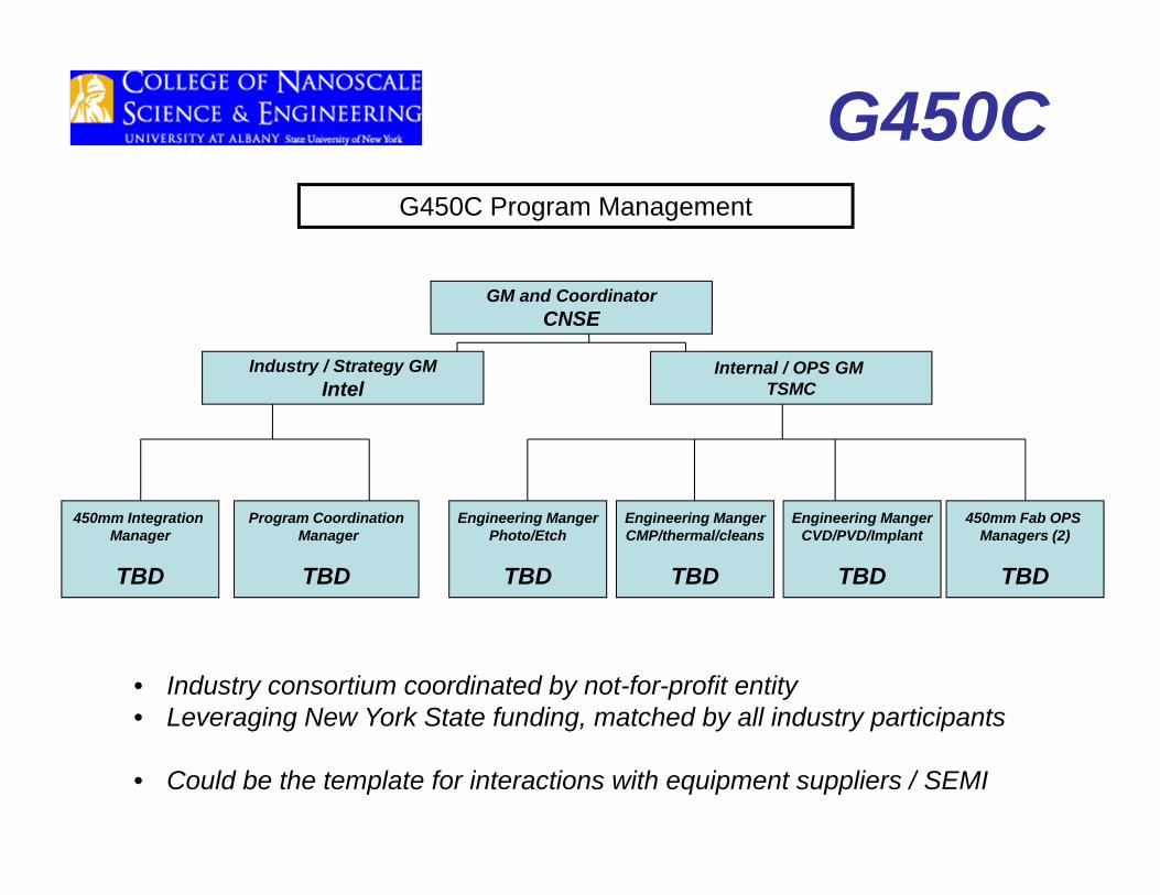
G450C
GM and CoordinatorCNSE
450mm Integration Manager
TBD
Program CoordinationManager
TBD
Engineering MangerCVD/PVD/Implant
TBD
450mm Fab OPS Managers (2)
TBD
Internal / OPS GM TSMC
Industry / Strategy GMIntel
Engineering MangerCMP/thermal/cleans
TBD
Engineering MangerPhoto/Etch
TBD
G450C Program Management
• Industry consortium coordinated by not-for-profit entity• Leveraging New York State funding, matched by all industry participants
• Could be the template for interactions with equipment suppliers / SEMI

G450C
• G450C as an umbrella initiative • Assure smooth and coordinated 300mm to 450mm wafer transition• Significant benefit to the industry and the State of New York. • New York state-of-the-art cleanroom and associated infrastructure.• Collective investments of
• G450C members, • State of New York, • Original equipment manufacturers, • Tool, material, and chemical suppliers, and • Facilities and infrastructure contractors.
• Assemble a critical mass of intellectual and physical assets.
G450C Mission
G450C
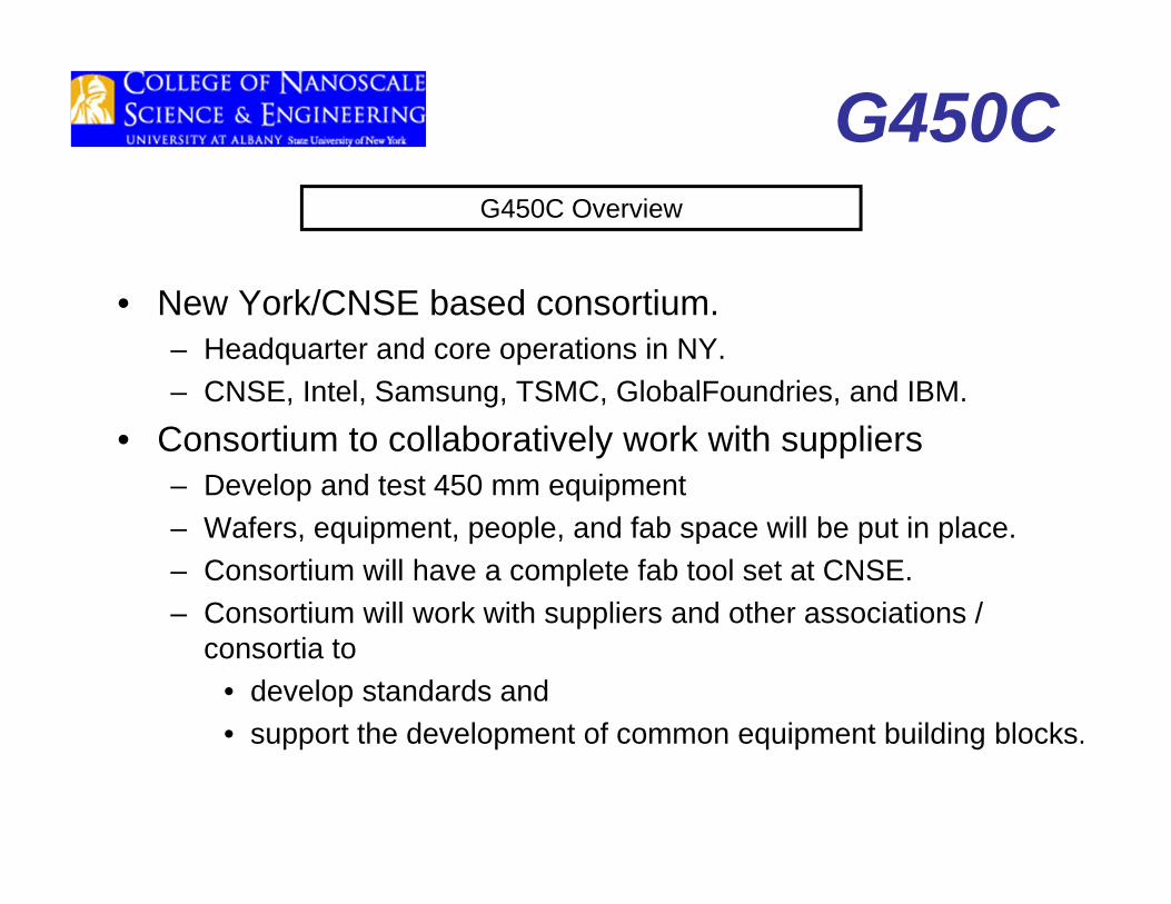
• New York/CNSE based consortium. – Headquarter and core operations in NY.– CNSE, Intel, Samsung, TSMC, GlobalFoundries, and IBM.
• Consortium to collaboratively work with suppliers – Develop and test 450 mm equipment– Wafers, equipment, people, and fab space will be put in place.– Consortium will have a complete fab tool set at CNSE.– Consortium will work with suppliers and other associations /
consortia to • develop standards and • support the development of common equipment building blocks.
G450C Overview

G450C
• Enable supplier development.• Support tool demonstrations.• Establish wafer support operations.• Enable innovation and do not slow scaling.• Demonstrate a full 450 mm fab tool set.
• Enable OEMs and tool makers to transition to 450mm in a highly coordinated fashion under a financially (New York) leveraged business strategy.
G450C Objectives

G450C
NFX –New CNSE Cleanroom
• >25,000 ft2 in NFX and NFN• NFX RFE in 4Q12
12

Late Tools?
– Expand Test Wafer operations to accelerate and support Supplier development and to support tool demonstrations
– Demonstrate a full 450 mm tool set with ~ 2 Suppliers for each of ~ 50 tool types (~100 demos) by 2014 / 2015
– Current status: RFQ sent, responses due in April
Projected Timeline2012 2013 2014 2015
LaunchG450C
Expand Test Wafer Operations
Demonstrate Full 450 mm Tool Set
Define Further Program Scope
Full‐flow 450 mm Tool Set and Process
@ CNSE• Objectives Beyond TW/Demo:
Imprint 193i EUV TBDLitho capability
(Phase 2)
(Phase 1)
G450C
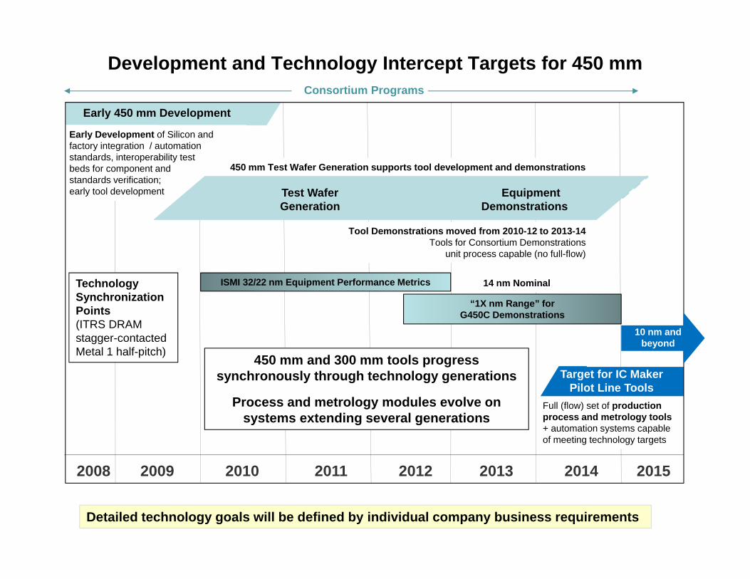
Development and Technology Intercept Targets for 450 mm
Detailed technology goals will be defined by individual company business requirements
2008 2009 2010 2011 2012 2013 2014 2015
Target for IC Maker Pilot Line Tools
Full (flow) set of production process and metrology tools+ automation systems capable of meeting technology targets
Early 450 mm Development
Early Development of Silicon and factory integration / automation standards, interoperability testbeds for component andstandards verification;early tool development
Consortium Programs
ISMI 32/22 nm Equipment Performance MetricsTechnologySynchronizationPoints(ITRS DRAM stagger-contacted Metal 1 half-pitch) 450 mm and 300 mm tools progress
synchronously through technology generations
Process and metrology modules evolve on systems extending several generations
10 nm and beyond
“1X nm Range” forG450C Demonstrations
Tool Demonstrations moved from 2010-12 to 2013-14Tools for Consortium Demonstrations
unit process capable (no full-flow)
450 mm Test Wafer Generation supports tool development and demonstrations
EquipmentDemonstrations
Test WaferGeneration
14 nm Nominal

450-mm Lithography Tool Alignment
1. Prototype tool*, 193i (G450C) 20132. Beta tool, 193 i/dry 20143. Beta tool, EUV 20154. Early production 193i/dry 20155. Early production EUV 20166. Production 193i/dry 20167. Production EUV 2017
* prototype tool: 14 nm patterning capability, (relax WPH and overlay )
450mm tool development will strategically align with 300mm EUV schedule to ensure both programs success.
G450C Aligned Schedule
G450C

G450C Summary
– Unique Industry Consortia – Academia - Government partnership
• Successful model applied to 450mm program• Associate memberships for suppliers possible
G450C