GL3520 - Компостер · GL3520 is a highly-compatible, high performance USB 3.0 hub...
33
Genesys Logic, Inc. GL3520 USB 3.0 Hub Controller Datasheet Revision 1.32 Jul. 15, 2011
Transcript of GL3520 - Компостер · GL3520 is a highly-compatible, high performance USB 3.0 hub...

Genesys Logic, Inc.
GL3520
USB 3.0 Hub Controller
Datasheet
Revision 1.32 Jul. 15, 2011

GL3520 Datasheet
©2011 Genesys Logic, Inc. - All rights reserved. Page 2
Copyright Copyright © 2011 Genesys Logic, Inc. All rights reserved. No part of the materials shall be reproduced in any form or by any means without prior written consent of Genesys Logic, Inc.
Ownership and Title Genesys Logic, Inc. owns and retains of its right, title and interest in and to all materials provided herein. Genesys Logic, Inc. reserves all rights, including, but not limited to, all patent rights, trademarks, copyrights and any other propriety rights. No license is granted hereunder.
Disclaimer
All Materials are provided “as is”. Genesys Logic, Inc. makes no warranties, express, implied or otherwise, regarding their accuracy, merchantability, fitness for any particular purpose, and non-infringement of intellectual property. In no event shall Genesys Logic, Inc. be liable for any damages, including, without limitation, any direct, indirect, consequential, or incidental damages. The materials may contain errors or omissions. Genesys Logic, Inc. may make changes to the materials or to the products described herein at anytime without notice.
Genesys Logic, Inc. 12F., No. 205, Sec. 3, Beixin Rd., Xindian Dist. 231,
New Taipei City, Taiwan
Tel : (886-2) 8913-1888
Fax : (886-2) 6629-6168
http://www.genesyslogic.com

GL3520 Datasheet
©2011 Genesys Logic, Inc. - All rights reserved. Page 3
Revision History
Revision Date Description
1.00 03/24/2011 First formal release
1.10 04/20/2011 Update QFN64 pin assignment
1.20 05/17/2011 Modify QFN88 package dimension, p.31 Modify Table 7.2-Operating Ranges, p.25
1.21 05/23/2011 Modify QFN64 package dimension, p.32
1.22 06/10/2011 Revise typo, p.26
1.30 06/17/2011 Update CH7.4 Power Consumption, p.26, 27
1.31 06/24/2011 Update crystal tolerance range, p.25
1.32 07/15/2011 Update CH3.2 Pin Descriptions, RTERM I/O type, p.12

GL3520 Datasheet
©2011 Genesys Logic, Inc. - All rights reserved. Page 4
Table of Contents
CHAPTER 1 GENERAL DESCRIPTION....................................................................... 7
CHAPTER 2 FEATURES.................................................................................................. 8
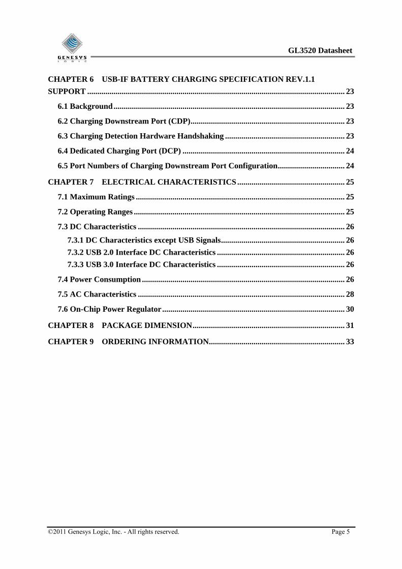
CHAPTER 3 PIN ASSIGNMENT..................................................................................... 9
3.1 Pinout.............................................................................................................................. 9
3.2 Pin Descriptions ........................................................................................................... 11
CHAPTER 4 BLOCK DIAGRAM.................................................................................. 14
CHAPTER 5 FUNCTION DESCRIPTION ................................................................... 15
5.1 General Description .................................................................................................... 15
5.1.1 USB 2.0 USPORT Transceiver........................................................................... 15
5.1.2 USB 3.0 USPORT Transceiver........................................................................... 15
5.1.3 PLL (Phase Lock Loop) ...................................................................................... 15
5.1.4 Regulator .............................................................................................................. 15
5.1.5 SPI Engine ............................................................................................................ 15
5.1.6 RAM/ROM/CPU.................................................................................................. 15
5.1.7 UTMI (USB 2.0 Transceiver Microcell Interface)............................................ 15
5.1.8 SIE (Serial Interface Engine).............................................................................. 15
5.1.9 Control/Status Register ....................................................................................... 15
5.1.10 Power Management Engine .............................................................................. 16
5.1.11 Router/Aggregator Engine................................................................................ 16
5.1.12 REPEATER ....................................................................................................... 16
5.1.13 TT........................................................................................................................ 16
5.1.14 CDP Control Logic ............................................................................................ 18
5.1.15 USB 3.0/USB 2.0 DSPORT Transceiver.......................................................... 18
5.2 Configuration and I/O Settings .................................................................................. 19
5.2.1 RESET Setting ..................................................................................................... 19
5.2.2 PGANG Setting.................................................................................................... 20
5.2.3 SELF/BUS Power Setting ................................................................................... 21
5.2.4 LED Connections................................................................................................. 21
5.2.5 Power Switch Enable Polarity ............................................................................ 21
5.2.6 Port Number Configuration ............................................................................... 22
5.2.7 Non-removable Port Configuration ................................................................... 22
GL3520 Datasheet
©2011 Genesys Logic, Inc. - All rights reserved. Page 5
CHAPTER 6 USB-IF BATTERY CHARGING SPECIFICATION REV.1.1
SUPPORT ............................................................................................................................... 23
6.1 Background.................................................................................................................. 23
6.2 Charging Downstream Port (CDP)............................................................................ 23
6.3 Charging Detection Hardware Handshaking ........................................................... 23
6.4 Dedicated Charging Port (DCP) ................................................................................ 24
6.5 Port Numbers of Charging Downstream Port Configuration................................. 24
CHAPTER 7 ELECTRICAL CHARACTERISTICS..................................................... 25
7.1 Maximum Ratings ....................................................................................................... 25
7.2 Operating Ranges ........................................................................................................ 25
7.3 DC Characteristics ...................................................................................................... 26
7.3.1 DC Characteristics except USB Signals............................................................. 26
7.3.2 USB 2.0 Interface DC Characteristics ............................................................... 26
7.3.3 USB 3.0 Interface DC Characteristics ............................................................... 26
7.4 Power Consumption .................................................................................................... 26
7.5 AC Characteristics ...................................................................................................... 28
7.6 On-Chip Power Regulator .......................................................................................... 30
CHAPTER 8 PACKAGE DIMENSION........................................................................... 31
CHAPTER 9 ORDERING INFORMATION................................................................... 33

GL3520 Datasheet
©2011 Genesys Logic, Inc. - All rights reserved. Page 6
List of Figures
Figure 3.1 - GL3520 QFN 88 Pin Pinout Diagram................................................................ 9
Figure 3.2 - GL3520 QFN 64 Pin Pinout Diagram.............................................................. 10
Figure 4.1 - Block Diagram ................................................................................................... 14
Figure 5.1 - Operating in USB 1.1 Schemes......................................................................... 17
Figure 5.2 - Operating in USB 2.0 Schemes......................................................................... 18
Figure 5.3 - Power on Reset Diagram................................................................................... 19
Figure 5.4 - Power on Sequence of GL3520 ......................................................................... 19
Figure 5.5 - Timing of PGANG Strapping........................................................................... 20
Figure 5.6 - GANG Mode Setting ......................................................................................... 20
Figure 5.7 - SELF/BUS Power Setting ................................................................................. 21
Figure 5.8 - LED Connection ................................................................................................ 21
Figure 7.1 - Vin(V5) vs Vout(V33)*...................................................................................... 30
Figure 8.1 - GL3520 88 Pin QFN Package ........................................................................... 31
Figure 8.2 - GL3520 64 Pin QFN Package ........................................................................... 32
List of Tables
Table 5.1 - Configuration by Power Switch Type ............................................................... 21
Table 7.1 - Maximum Ratings............................................................................................... 25
Table 7.2 - Operating Ranges................................................................................................ 25
Table 7.3 - DC Characteristics except USB Signals ............................................................ 26
Table 9.1 - Ordering Information......................................................................................... 33

GL3520 Datasheet
©2011 Genesys Logic, Inc. - All rights reserved. Page 7
CHAPTER 1 GENERAL DESCRIPTION
GL3520 is a highly-compatible, high performance USB 3.0 hub controller, which integrates Genesys Logic own self-developed USB 3.0 Super Speed transmitter/receiver physical layer (PHY) and USB 2.0 High-Speed PHY. It supports Super Speed, Hi-Speed, and Full-Speed USB connections and is fully backward compatible to all USB 2.0 and USB 1.1 hosts. GL3520 is a premium 4 port MTT Hub solution, implementing multiple TT* (Note1) architecture that provide dedicated TT* to each downstream (DS) ports, which guarantee Full-Speed(FS) data passing bandwidth when multiple FS device perform heavy loading operations. GL3520 also complies with USB-IF battery charging specification rev1.1, which can support fast charging function, allowing portable device can draw up to 1.5A from GL3520 charging downstream ports (CDP1) or dedicated charging port (DCP2). So it can enable systems to fast charge handheld devices even during “Sleep” and “Power-off” modes. There are two available packages: QFN88(10x10mm) and QFN64(8x8mm). Summarize as below table.
Package Type # of DS Ports Power Mgmt. LED Support FW Upgrade
QFN 88 4 Individual/Gang Green/Amber SPI Flash
QFN 64 4 Gang Green SPI Flash
GL3520 Package – Feature Summary
*Note: TT (transaction translator) implements the control logic defined in section 11.14 ~ 11.22 of USB specification revision 2.0. TT basically handles the unbalanced traffic speed between the USPORT (operating in HS) and DSPORTS (operating in FS/LS) of hub.
1 CDP, charging downstream port, the Battery Charging Rev.1.1-compliant USB port that does data communication and charges device up to 1.5A. 2 DCP, dedicated charging port, the Battery Charging Rev.1.1-compliant USB port that only charges devices up to 1.5A, similar to wall chargers.

GL3520 Datasheet
©2011 Genesys Logic, Inc. - All rights reserved. Page 8
CHAPTER 2 FEATURES
Compliant with USB Specification Revision 3.0 - Upstream port supports super speed(SS) high speed(HS) and full speed(FS) traffic - Downstream ports support SS, HS, FS, and low speed(LS) traffic - 1 control pipe(endpoint 0, 64-byte data payload) and 1 interrupt pipe(endpoint 1, 1-byte data payload) - Backward compatible to USB specification Revision 2.0/1.1
Compliant with USB Battery Charging Revision v1.1 - Turning its downstream port from a standard downstream port (SDP) into charging downstream port
(CDP) or Dedicated Charging Ports (DCP). - Enables portable device to charge from VBUS even when the USB bus is in suspend.
On-chip 8-bit micro-processor - RISC-like architecture - USB optimized instruction set - 1 cycle instruction execution( maximum) - Performance: 12 MIPS @ 12MHz( maximum) - With 256-byte RAM, 16K-byte internal ROM & 16K-byte SRAM
Multi Transaction Translator(TT) architecture - Provides dedicated TT control logics for each downstream port - Superior performance when multiple FS devices operate concurrently
Integrated USB transceiver - Improve output drivers with slew-rate control for EMI reduction - Internal power-fail detection for ESD recovery
Smart power management
- Support USB3.0 U0/U1/U2/U3 power management states - Support individual / gang mode over-current detection for all downstream ports. - Support both low/high-enabled power switches. - Automatic switching between self-powered and bus-powered modes.
Low BOM cost - Single external 25 MHz crystal / Oscillator clock input - Built-in upstream port 1.5KΩ pull-up and downstream port 15KΩ pull-down resistors
Flexible design - Configurable 4/3/2 downstream ports - Support partial/full in-system programming firmware upgrade by SPI-flash - Support compound-device (non-removable in downstream ports) by I/O pin configuration
Available package type - QFN 88 (10x10mm) - QFN 64 (8x8mm)
Applications:
- Stand-alone USB hub / USB docking - Netbook/Smartbook/MID/Motherboard on-board applications - Monitor built-in hub - TV built-in hub - Other Consumer electronics built-in hub application - Compound device to support USB hub function such as hub reader applications
GL3520 Datasheet
©2011 Genesys Logic, Inc. - All rights reserved. Page 9
CHAPTER 3 PIN ASSIGNMENT
3.1 Pinout
QFN - 88
44
43
42
41
40
39
38
37
36
35
34
33
32
31
30
29
28
27
26
25
24
23
DVDD12
VP12
RXP_DS4
RXN_DS4
GND
TXP_DS4
TXN_DS4
VP12
VP12
RXP_DS3
RXN_DS3
GND
TXP_DS3
TXN_DS3
VP12
VP12
RXP_DS2
RXN_DS2
GND
TXP_DS2
TXN_DS2
VP12
1 2 3 4 5 6 7 8 9 10 11 12 13 14 15 16 17 18 19 20 21 22
PA
MB
ER
4
PWR
EN
4J
RT
ER
M
GN
D
VP
33C
R X1
X2
VP1
2
TX
N_U
P
TX
P_U
P
GN
D
RX
N_U
P
RX
P_U
P
VP1
2
VP1
2
TX
N_D
S1
TX
P_D
S1
GN
D
RX
N_D
S1
RX
P_D
S1
VP1
2
GN
D
66 65 64 63 62 61 60 59 58 57 56 55 54 53 52 51 50 49 48 47 46 45
AV
DD
DP2
DM
2
AV
DD
DP1
DM
1
DP0
DM
0
DV
DD
DV
DD
12
PA
MB
ER
3
VB
US
OV
CU
R4J
PWR
EN
1J
PAM
BE
R1
P_S
PI_C
Z
P_S
PI_C
K
DV
DD
12
PG
RE
EN
3
PWR
EN
3J
PWR
EN
2J
OV
CU
R2J
67
68
69
70
71
72
73
74
75
76
77
78
79
80
81
82
83
84
85
86
87
88
GND
DM3
DP3
AVDD
DM4
DP4
DVDD
PGANG
DVDD12
TEST
OVCUR3J
OVCUR1J
PGREEN1
P_SPI_DO
P_SPI_DI
PSELF
RESETJ
PGREEN2
V33
V5
PAMBER2
PGREEN4
Figure 3.1 - GL3520 QFN 88 Pin Pinout Diagram

GL3520 Datasheet
©2011 Genesys Logic, Inc. - All rights reserved. Page 10
DM3
DP3
AVDD
DM4
DP4
DVDD
PGANG
DVDD12
OVCUR1J
P_SPI_DO
P_SPI_DI
PSELF
RESETJ
DVDD12
V33
V5
RXN_DS4
TXP_DS4
TXN_DS4
VP12
VP12
RXP_DS3
RXN_DS3
TXP_DS3
TXN_DS3
VP12
VP12
RXP_DS2
RXN_DS2
TXP_DS2
TXN_DS2
VP12
QFN - 64
31
30
29
28
27
26
25
24
23
22
21
20
19
18
17
32
50
51
52
53
54
55
56
57
58
59
60
61
62
63
64
49
Figure 3.2 - GL3520 QFN 64 Pin Pinout Diagram

GL3520 Datasheet
©2011 Genesys Logic, Inc. - All rights reserved. Page 11
3.2 Pin Descriptions
USB Interface
Pin Name QFN 88 QFN 64 Type Description
TXN_UP TXP_UP
9 10
6 7
O USB 3.0 Differential Data Transmitter TX-/TX+ of USPORT
RXN_UP RXP_UP
12 13
8 9
I USB 3.0 Differential Data Receiver RX-/RX+ of USPORT
TXN_DS1 TXP_DS1
16 17
12 13
O USB 3.0 Differential Data Transmitter TX-/TX+ of DSPORT1
RXN_DS1 RXP_DS1
19 20
14 15
I USB 3.0 Differential Data Receiver RX-/RX+ of DSPORT1
TXN_DS2 TXP_DS2
24 25
18 19
O USB 3.0 Differential Data Transmitter TX-/TX+ of DSPORT2
RXN_DS2 RXP_DS2
27 28
20 21
I USB 3.0 Differential Data Receiver RX-/RX+ of DSPORT2
TXN_DS3 TXP_DS3
32 31
24 25
O USB 3.0 Differential Data Transmitter TX-/TX+ of DSPORT3
RXN_DS3 RXP_DS3
34 35
26 27
I USB 3.0 Differential Data Receiver RX-/RX+ of DSPORT3
TXN_DS4 TXP_DS4
38 39
30 31
O USB 3.0 Differential Data Transmitter TX-/TX+ of DSPORT4
RXN_DS4 RXP_DS4
41 42
32 33
I USB 3.0 Differential Data Receiver RX-/RX+ of DSPORT4
DM0,DP0 59,60 41 42
B USB 2.0 DM/DP for USPORT
DM1, DP1 61,62 43 44
B USB 2.0 DM/DP for DSPORT1
DM2, DP2 64,65 46 47
B USB 2.0 DM/DP for DSPORT2
DM3, DP3 68, 69 49 50
B USB 2.0 DM/DP for DSPORT3
DM4, DP4 71,72 52 53
B USB 2.0 DM/DP for DSPORT4
Hub Interface
Pin Name QFN 88 QFN 64 Type Description
PGREEN1~4 79,84, 48,88
- B (pd) Green LED indicator for DSPORT1~4
PAMBER1~4 52,87,56,1 - B (pd) Amber LED indicator for DSPORT1~4
PWREN1~4J 53,46,47,2 37, B Active low. Power enable output for DSPORT1~4 PWREN1# is the only power-enable output for GANG mode.
OVCUR1~4J 78,45,77,5
4 57 I (pu)
Active low. Over current indicator for DSPORT1~4 OVCUR1# is the only over current flag for GANG mode.
PGANG 74 55 I Default put in input mode after power-on reset. Individual/gang mode is strapped during this period.
PSELF 82 60 I 0: GL3520 is bus-powered. 1: GL3520 is self-powered.

GL3520 Datasheet
©2011 Genesys Logic, Inc. - All rights reserved. Page 12
Clock and Reset Interface
Pin Name QFN 88 QFN 64 Type Description
X1 6 3 I Crystal / OSC clock input
X2 7 4 O Crystal clock output.
RESETJ 83 61 I (pd) Active low. External reset input, default pull high 10KΩ. When RESET# = low, whole chip is reset to the initial state.
SPI Interface
Pin Name QFN 88 QFN 64 Type Description
P_SPI_CK 50 35 B For SPI data clock
P_SPI_CZ 51 36 B For SPI data chip enable
P_SPI_DO 80 58 B For SPI data Input
P_SPI_DI 81 59 B For SPI data Output
Power/Ground Interface
Pin Name QFN 88 QFN 64 Type Description
VP33CR 5 2 P Analog 3.3V power input
VP12 8,14,15,21,23
29,30,36,37,43 5,10.11,1617,22,23,28,29,34
P Analog 1.2V power input for Analog circuit
DVDD12 44,49,57,75 39,56,62 P 1.2V digital power input for digital circuits
DVDD 58,73 40,54 P 3.3V digital power input for digital circuits
AVDD 63,66,70 45,48,51 P Analog 3.3V power input
GND 4,11,18,22
26,33,40,67- P Digital/Analog ground
VBUS 55 38 I VBUS valid input
V33 85 63 P 5V-to-3.3V regulator Vout & 3.3 input
V5 86 64 P 5V Power input. It need be NC if using external regulator
Miscellaneous Interface
Pin Name QFN 88 QFN 64 Type Description
RTERM 3 1 A A 680ohm resister must be connected between RTERM and Ground
TEST 76 - B (pd) TEST: 0: Normal operation. 1: Chip will be put in test mode.
Note: Analog circuits are quite sensitive to power and ground noise. PCB layout must take care the power routing and the ground plane. For detailed information, please refer to GL3520 Design Guideline.
Notation:
Type O Output I Input B Bi-directional P Power / Ground A Analog

GL3520 Datasheet
©2011 Genesys Logic, Inc. - All rights reserved. Page 13
pu Internal pull up pd Internal pull down

GL3520 Datasheet
©2011 Genesys Logic, Inc. - All rights reserved. Page 14
CHAPTER 4 BLOCK DIAGRAM
Figure 4.1 - Block Diagram

GL3520 Datasheet
©2011 Genesys Logic, Inc. - All rights reserved. Page 15
CHAPTER 5 FUNCTION DESCRIPTION
5.1 General Description
5.1.1 USB 2.0 USPORT Transceiver
USB 2.0 USPORT (upstream port) transceiver is the analog circuit that supports both full-speed and high-speed electrical characteristics defined in chapter 7 of USB specification revision 2.0. USPORT transceiver will operate in full-speed electrical signaling when GL3520 is plugged into a 1.1 host/hub. USPORT transceiver will operate in high-speed electrical signaling when GL3520 is plugged into a 2.0 host/hub.
5.1.2 USB 3.0 USPORT Transceiver
USB 3.0 USPORT (upstream port) transceiver is the analog circuit that has elastic buffer and supports receiver detection, data serialization and de-serialization. Besides, it has PIPE interface with SuperSpeed Link Layer
5.1.3 PLL (Phase Lock Loop)
PLL generates the clock sources for the whole chip. The generated clocks are proven quite accurate that help in generating high speed signal without jitter.
5.1.4 Regulator
GL3520 build in internal regulator converts 5V input to 3.3V output. 5.1.5 SPI Engine
SPI engine is to move code from external flash to the internal RAM.
5.1.6 RAM/ROM/CPU
The micro-processor unit of GL3520 is an 8-bit RISC processor with 16K-byte ROM and 256-bytes RAM. It operates at 12MIPS of 12 MHz clock( maximum) to decode the USB command issued from host and then prepares the data to respond to the host.
5.1.7 UTMI (USB 2.0 Transceiver Microcell Interface)
UTMI handles the low level USB protocol and signaling. It’s designed based on the Intel’s UTMI specification 1.01. The major functions of UTMI logic are to handle the data and clock recovery, NRZI encoding/decoding, Bit stuffing /de-stuffing, supporting USB 2.0 test modes, and serial/parallel conversion.
5.1.8 SIE (Serial Interface Engine)
SIE handles the USB protocol defined in chapter 8 of USB specification revision 2.0. It co-works with μC to play the role of the hub kernel. The main functions of SIE include the state machine of USB protocol flow, CRC check, PID error check, and timeout check. Unlike USB 1.1, bit stuffing/de-stuffing is implemented in UTMI, not in SIE.
5.1.9 Control/Status Register
Control/Status register is the interface register between hardware and firmware. This register contains the information necessary to control endpoint0 and endpoint1 pipelines. Through the firmware based architecture, GL3520 possesses higher flexibility to control the USB protocol easily and correctly.

GL3520 Datasheet
©2011 Genesys Logic, Inc. - All rights reserved. Page 16
5.1.10 Power Management Engine
The power management of GL3520 is compliant with USB 3.0 specification. When operates in SuperSpeed mode, GL3520 supports U0, U1, U2 and U3 power states. U0 is the functional state. U1 and U2 are lower power states compared to U0. U1 is a low power state with fast exit to U0; U2 is a low power state which saves more power than U1, with slower exit to U0. U3 is suspend state, which is the most power-saving state, with tens of milliseconds exit to U0. Unlike USB 2.0, SuperSpeed packet traffic is unicast rather than broadcast. Packet only travels the direct path in-between host and the target device. SuperSpeed traffic will not reach an unrelated device. When enabled for U1/U2 entry, and there is no pending traffic within comparable exit latency, GL3520 will initiate U1/U2 entry to save the power. On the other hand, the link partner of GL3520 may also initiate U1/U2 entry. In this case, GL3520 will accept or reject low power state entry according to its internal condition.
5.1.11 Router/Aggregator Engine
Router/Aggregator Engine implement the control logic defined in Ch10 of USB3.0 specification. Router/Aggregator Engine use smart method for route packet to device or aggregate packet to host.
5.1.12 REPEATER
Repeater logic implements the control logic defined in section 11.4 and section 11.7 of USB specification revision 2.0. REPEATER controls the traffic flow when upstream port and downstream port are signaling in the same speed. In addition, REPEATER will generate internal resume signal whenever a wakeup event is issued under the situation that hub is globally suspended.
5.1.13 TT
TT(Transaction Translator) implements the control logic defined in section 11.14 ~ 11.22 of USB specification revision 2.0. TT basically handles the unbalanced traffic speed between the USPORT (operating in HS) and DSPORTS (operating in FS/LS) of hub. GL3520 adopts multiple TT architecture to provide the most performance effective solution. Multiple TT provides control logics for each downstream port respectively.
5.1.13.1 Connected to 1.1 Host/Hub If an USB 2.0 hub is connected to the downstream port of an USB 1.1 host/hub, it will operate in USB 1.1 mode. For an USB 1.1 hub, both upstream direction traffic and downstream direction traffic are passing through REPEATER. That is, the REPEATER/TT routing logic will route the traffic channel to the REPEATER.

GL3520 Datasheet
©2011 Genesys Logic, Inc. - All rights reserved. Page 17
USB 1.1 Host/Hub
REPEATER TT
DSPORT operatingin FS/LS signaling
USPORToperatingin FS signaling
Traffic channel is routed toREPEATER
TT
Figure 5.1 - Operating in USB 1.1 Schemes
5.1.13.2 Connected to USB 2.0 Host/Hub If an USB 2.0 hub is connected to an USB 2.0 host/hub, it will operate in USB 2.0 mode. The upstream port signaling is in high speed with bandwidth of 480 Mbps under this environment. The traffic channel will then be routed to the REPEATER when the device connected to the downstream port is signaling also in high speed. On the other hand, the traffic channel will then be routed to TT when the device connected to the downstream port is signaling in full/low speed.

GL3520 Datasheet
USB 2.0 Host/Hub
REPEATER TT
USPORToperatingin HS signaling
HS vs. FS/LS:Traffic channelis routed to TT
HS vs. HS:Traffic channel is routed to REPEATER
DSPORT operatingin HS signaling
DSPORT operatingin FS/LS signaling
TT
Figure 5.2 - Operating in USB 2.0 Schemes
5.1.14 CDP Control Logic
CDP (charging downstream port) control logic implements the logic defined in USB Battery charging specification revision 1.1. The major function of it is to control DSPORT Transceiver to make handshake with a portable device which is compliant with USB Battery charging spec rev1.1 as well. After recognizing charging detection each other, portable device will draw up to 1.5A from VBUS to fast charge its battery.
5.1.15 USB 3.0/USB 2.0 DSPORT Transceiver
DSPORT transceiver is the analog circuit that supports high-speed, full-speed, and low-speed electrical characteristics. In addition, each DSPORT transceiver accurately controls its own squelch level to detect the detachment and attachment of devices.
©2011 Genesys Logic, Inc. - All rights reserved. Page 18

GL3520 Datasheet
©2011 Genesys Logic, Inc. - All rights reserved. Page 19
5.2 Configuration and I/O Settings
5.2.1 RESET Setting
GL3520’s power on reset can either be triggered by external reset or internal power good reset circuit. The external reset pin, RESETJ, is connected to upstream port Vbus (5V) to sense the USB plug / unplug or 5V voltage drop. The reset trigger voltage can be set by adjusting the value of resistor R1 and R2 (Suggested value refers to schematics) GL3520’s internal reset is designed to monitor silicon’s internal core power (1.2V) and initiate reset when unstable power event occurs. The power on sequence will start after the power good voltage has been met, and the reset will be released after approximately 40 μS after power good. GL3520’s reset circuit as depicted in the picture.
Global Reset#
Int. 3.3V power-good detection circuit input
(USB PHY reset)
INT
EXT
Ext. VBUS power-good detection circuit input
(Pin"RESET#")VBUS
(External 5V)
PCB Silicon
R1
R2
PinVBUS
Figure 5.3 - Power on Reset Diagram
To fully control the reset process of GL3520, we suggest the reset time applied in the external reset circuit should longer than that of the internal reset circuit. Timing of POR is illustrated as below figure.
Figure 5.4 - Power on Sequence of GL3520

GL3520 Datasheet
©2011 Genesys Logic, Inc. - All rights reserved. Page 20
5.2.2 PGANG Setting
To save pin count, GL3520 uses the same pin to decide individual/gang mode as well as to output the suspend flag. The individual/gang mode is decided within 21us after power on reset. Then, about 50ms later, this pin is changed to output mode. GL3520 outputs the suspend flag once it is globally suspended. For individual mode, a pull low resister greater than 100KΩ should be placed. For gang mode, a pull high resister which greater than 100KΩ should be placed. In figure 5.6, we also depict the suspend LED indicator schematics. It should be noticed that the polarity of LED must be followed, otherwise the suspend current will be over spec limitation (2.5mA).
Figure 5.5 - Timing of PGANG Strapping
Figure 5.6 - GANG Mode Setting

GL3520 Datasheet
©2011 Genesys Logic, Inc. - All rights reserved. Page 21
5.2.3 SELF/BUS Power Setting
By setting PSELF, GL3520 can be configured as a bus-power or a self-power hub.
Figure 5.7 - SELF/BUS Power Setting
5.2.4 LED Connections
GL3520 controls the LED lighting according to the flow defined in section 11.5.3 of Universal Serial Bus Specification Revision2.0. Both manual mode and Automatic mode are supported in GL3520. When GL3520 is globally suspended, GL3520 will turn off the LED to save power.
AMBER/GREEN
Inside GL3520On PCB
DGND
LED
Figure 5.8 - LED Connection
5.2.5 Power Switch Enable Polarity
Both low/high-enabled power switches are supported. It is determined by jumper setting. The power switch polarity will be configured by the state of pin AMBER2, as the following table:
Table 5.1 - Configuration by Power Switch Type
AMBER2 Power Switch Enable Polarity
0 Low-active
1 High-active
Note: When AMBER2=1, the external resistor of PWREN1~4 need pull down

GL3520 Datasheet
©2011 Genesys Logic, Inc. - All rights reserved. Page 22
5.2.6 Port Number Configuration
Number of downstream port can be configured as 1/2/3/4 ports by firmware configuration. The detail setting information please refers to the GL3520 Firmware ISP Tool User Guide document. 5.2.7 Non-removable Port Configuration
For compound application or embedded system, downstream ports that always connected inside the system can be set as non-removable by firmware configuration. The detail setting information please refers to the GL3520 Firmware ISP Tool User Guide document.

GL3520 Datasheet
©2011 Genesys Logic, Inc. - All rights reserved. Page 23
CHAPTER 6 USB-IF BATTERY CHARGING SPECIFICATION REV.1.1 SUPPORT
6.1 Background
The USB ports on personal computers are convenient places for portable devices to draw current for charging their batteries. This convenience has led to the creation of dedicated chargers that simply expose a USB standard-A receptacle. This allows portable devices to use the same USB cable to charge from either a PC or from a dedicated charger. If a portable device is attached to a USB host or hub, then the USB 2.0 specification requires that after connecting, a portable device must draw less than:
2.5 mA average if the bus is suspended 100 mA maximum if bus is not suspended and not configured 500 mA maximum if bus is not suspended and configured for 500 mA
If a portable device is attached to a charging host or hub, it is allowed to draw a current up to 1.5A or 900mA, regardless of suspend. In order for a portable device determine how much current it is allowed to draw from an upstream USB port, the USB-IF Battery Charging specification defines the mechanisms that allow the portable device to distinguish between either a USB standard host, hub or a USB charging host. Since portable device can be attached to USB charging ports from various manufactures, it is important that all USB charging ports behave the same way. This specification also defines the requirements for a USB chargers and charging downstream ports. 6.2 Charging Downstream Port (CDP)
GL3520 supports battery charging detection, turning its downstream port from a standard downstream port (SDP) into charging downstream port (CDP). GL3520 will make physical layer handshaking when a portable device (PD) compliant with BC rev1.1 attaches to its downstream port. After physical layer handshaking, PD is allowed to draw more current up to 900mA or 1.5A, depending on PD is configured as High-Speed (900mA) or Full-Speed/Low-Speed (1.5A) device.
6.3 Charging Detection Hardware Handshaking
Once the charging downstream port of GL3520 enabled, it will monitor the VDP_SRC on D+ line anytime. When BCv1.1 compliant PD attached to the downstream port, it will drive VDP_SRC on D+ line to initiate handshaking with charging downstream port. GL3520 will response on its D- line by VDM_SRC and keep in a certain period of time and voltage level. The portable device will accept this handshake on its D- line in correct timing period and voltage level and then turns off its VDP_SRC on D+ line. GL3520 will recognize that charging negotiation is finished by counting time between PD turning on and off its VDP_SRC. After that, the portable device can start to draw more current at VBUS to charge its battery more rapidly. It can draw current up to 1.5A or 900mA, depending on PD is configured as HS, FS or LS device. If no response on D- line returns, the portable device will recognize that it is attached to a standard downstream port, not a charging port.

GL3520 Datasheet
©2011 Genesys Logic, Inc. - All rights reserved. Page 24
6.4 Dedicated Charging Port (DCP)
GL3520 also support dedicated charging port, which is a downstream port on a device that outputs power through a USB connector, but is not capable of enumerating a downstream device. With the adequate system circuit design, GL3520 will turn its downstream port from a standard downstream port (SDP) into dedicated charging port (DCP), i.e short the D+ line to the D- line, to let PD draw current up to 1.5A. The detail system design information please refers to the GL3520 Design Guide document. 6.5 Port Numbers of Charging Downstream Port Configuration
Numbers of charging downstream port can be configured as 1/2/3/4 ports by firmware configuration. The detail setting information please refers to the GL3520 Firmware ISP Tool User Guide document.

GL3520 Datasheet
©2011 Genesys Logic, Inc. - All rights reserved. Page 25
CHAPTER 7 ELECTRICAL CHARACTERISTICS
7.1 Maximum Ratings
Table 7.1 - Maximum Ratings
Symbol Parameter Min. Max. Unit
V5 5V Power Supply -0.5 +6.0 V
VDD 3.3V Power Supply -0.5 +3.6 V
VDDcore 1.2VPower Supply -0.5 +1.32 V
VIN 3.3V Input Voltage for digital I/O(EE_DO) pins -0.5 +3.6 V
Vincore 1.2V -0.5 +1.32 V
VINOD Open-Drain Input (Ovcur1-4,Pself,Reset) -0.5 +5.5 V
VINUSB Input Voltage for USB signal (DP, DM) pins -0.5 +3.6 V
TS Storage Temperature under bias -60 +100 oC
FOSC Frequency 25 MHz 0.03%
7.2 Operating Ranges
Table 7.2 - Operating Ranges
Symbol Parameter Min. Typ. Max. Unit
V5 5V Power Supply 4.75 5.0 5.25 V
VDD 3.3V Power Supply 3.0 3.3 3.6 V
VDDcore 1.2V Power Supply 1.15 1.2 1.32 V
VIND Input Voltage for digital I/O pins -0.5 3.3 3.6 V
VINUSB Input Voltage for USB signal (DP, DM) pins 0.5 3.3 3.6 V
TA Ambient Temperature 0 - 70 oC
TJ Absolute maximum junction temperature 0 - 125 oC

GL3520 Datasheet
©2011 Genesys Logic, Inc. - All rights reserved. Page 26
7.3 DC Characteristics
7.3.1 DC Characteristics except USB Signals
Table 7.3 - DC Characteristics except USB Signals
Symbol Parameter Min. Typ. Max. Unit
VDD Power Supply Voltage 3 3.3 3.6 V
VIL LOW level input voltage - - 0.8 V
VIH HIGH level input voltage 2.0 - - V
VTLH LOW to HIGH threshold voltage 1.4 1.5 1.6 V
VTHL HIGH to LOW threshold voltage 0.87 0.94 0.99 V
VOL LOW level output voltage when IOL=8mA - - 0.4 V
VOH HIGH level output voltage when IOH=8mA 2.4 - - V
IOLK Leakage current for pads with internal pull up or pull down resistor
- - 30 A
RDN Pad internal pull down resister 81K 103K 181K Ω
RUP Pad internal pull up resister 81K 103K 181K Ω
7.3.2 USB 2.0 Interface DC Characteristics The GL3520 conforms to DC characteristics for Universal Serial Bus specification rev. 2.0. Please refer to this specification for more information.
7.3.3 USB 3.0 Interface DC Characteristics The GL3520 conforms to DC characteristics for Universal Serial Bus specification rev.3.0. Please refer to this specification for more information.
7.4 Power Consumption
Symbol USB 3.0 Host Number of USB 3.0 Active Ports Config. Read Write Unit
4 0.19 0.96 0.93 W
3 0.18 0.78 0.80 W
2 0.18 0.66 0.66 W
1 0.17 0.51 0.50 W
ICC
USPORT Config 0.01 W

GL3520 Datasheet
©2011 Genesys Logic, Inc. - All rights reserved. Page 27
Symbol USB 3.0 Host Number of USB 2.0 Active Ports Config. Read Write Unit
4 0.29 0.38 0.34 W
3 0.25 0.31 0.30 W
2 0.22 0.25 0.26 W
1 0.18 0.19 0.20 W
ICC
USPORT Config 0.01 W
Note:
Test result represents silicon level operating current, without considering additional power consumption contributed by external over-current protection circuit such as power switch or polyfuse.

GL3520 Datasheet
©2011 Genesys Logic, Inc. - All rights reserved. Page 28
7.5 AC Characteristics
GL3520 can support SPI( mode0) for on-line firmware upgrade.

GL3520 Datasheet
©2011 Genesys Logic, Inc. - All rights reserved. Page 29
Symbol Parameter Min. Typ. Max. Unit
fCT Clock Frequency for fast read mode 0 - 100 MHz
fC Clock Frequency for read mode 0 - 33 MHz
tRI Input Rise Time - - 8 ns
tFI Input Fall Time - - 8 ns
tCXH SCK High Time 4 - - ns
tCXL SCK Low Time 4 - - ns
tCEH CE# High Time 25 - - ns
tCS CE# Setup Time 10 - - ns
tCH CE# Hold Time 5 - - ns
tDS Data in Setup Time 2 - - ns
tDH Data in Hold Time 2 - - ns
tHS Hold Setup Time 15 - - ns
tHD Hold Time 15 - - ns
tV Output Valid - - 8 ns
tOH Output Hold Time Normal Mode 0 - - ns
tLZ Hold to Output Low Z - - 200 ns
tHZ Hold to Output High Z - - 200 ns
tDIS Output Disable Time - - 100 Ns
tEC Secter/Block/Chip Erase Time - 40 100 ms
tPP Page Program Time - 2 5 ms
tW Write Status Register Time - 40 100 ms
tVCS Vcc Set-up Time 50 - - μs
GL3520 Datasheet
©2011 Genesys Logic, Inc. - All rights reserved. Page 30
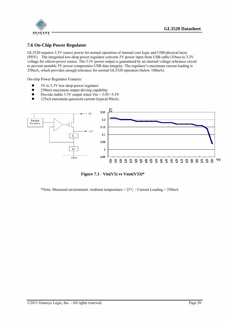
7.6 On-Chip Power Regulator
GL3520 requires 3.3V source power for normal operation of internal core logic and USB physical layer (PHY). The integrated low-drop power regulator converts 5V power input from USB cable (Vbus) to 3.3V voltage for silicon power source. The 3.3V power output is guaranteed by an internal voltage reference circuit to prevent unstable 5V power compromise USB data integrity. The regulator’s maximum current loading is 250mA, which provides enough tolerance for normal GL3520 operation (below 100mA). On-chip Power Regulator Features:
5V to 3.3V low-drop power regulator 250mA maximum output driving capability Provide stable 3.3V output when Vin = 3.4V~5.5V 125uA maximum quiescent current (typical 80uA).
Figure 7.1 - Vin(V5) vs Vout(V33)*
*Note: Measured environment: Ambient temperature = 25 / Current Loading = 250mA

GL3520 Datasheet
©2011 Genesys Logic, Inc. - All rights reserved. Page 31
CHAPTER 8 PACKAGE DIMENSION
Figure 8.1 - GL3520 88 Pin QFN Package

GL3520 Datasheet
©2011 Genesys Logic, Inc. - All rights reserved. Page 32
Figure 8.2 - GL3520 64 Pin QFN Package

GL3520 Datasheet
©2011 Genesys Logic, Inc. - All rights reserved. Page 33
CHAPTER 9 ORDERING INFORMATION
Table 9.1 - Ordering Information
Part Number Package Material Version Status
GL3520-OVYXX QFN 88 Green Package XX Available
GL3520-OSYXX QFN 64 Green Package XX Available