Giga Connections, Inc. is a licensed manufacture that works closely with circuit board houses to...
19
Giga Connections, Inc. is a licensed manufacture that works closely with circuit board houses to Diamond Plate (DP) FR4, Flex and Kapton substrates for 3 rd party designs. The Conductive Diamond Plating forms an electrical interconnect that demonstrates an ~1% impedance discontinuity, similar to a soldered junction, without any observable inductance or capacitance, thereby achieving a connection bandwidth beyond 40 GHz. Giga Connections Inc. has successfully developed 40 GHz DP Interposers for Device Test Sockets used in 10 G/bit communication systems and radiation device testing. Other applications include the plating of Flex circuit contact pads used in VLSI test-head connectors and instrument test probes. Giga Connections, inc 4182 Center Park Dr. Colorado Springs, CO 80916 1
-
Upload
michael-brown -
Category
Documents
-
view
215 -
download
0
Transcript of Giga Connections, Inc. is a licensed manufacture that works closely with circuit board houses to...

Giga Connections, Inc. is a licensed manufacture that works closely with circuit board houses to Diamond Plate (DP) FR4, Flex and Kapton substrates for 3rd party designs. The Conductive Diamond Plating forms an electrical interconnect that demonstrates an ~1% impedance discontinuity, similar to a soldered junction, without any observable inductance or capacitance, thereby achieving a connection bandwidth beyond 40 GHz.
Giga Connections Inc. has successfully developed 40 GHz DP Interposers for Device Test Sockets used in 10 G/bit communication systems and radiation device testing. Other applications include the plating of Flex circuit contact pads used in VLSI test-head connectors and instrument test probes.
Giga Connections, inc4182 Center Park Dr.
Colorado Springs, CO 80916www.gigaconnections.com
1

Conductive Diamond Plating (CDP) Description
The CDP interposer uses conductive diamond particles to form a superior, multi-point connection system. The CDP surface pierces any contaminants on either the DUT leads or test contacts. The resulting contact resistance is fewer than 5 milliohms with no measurable inductance or capacitance after thousands of mate/demate cycles. The controlled impedance material is electrically invisible, requires as little as 10-15 grams contact force, and resists oil and dirt contaminates.
CDP has been used in military systems, including super computers and satellites meeting all military environmental specifications. CDP enables 10 – 40+ G/bit devices to perform the same or better within socket applications than if they were soldered directly to the board, thereby opening opportunities for a new lead- free interconnect technology.
2

Conductive Diamond Pin-less Interposer™
Specifications
Slides 4-10 describe the GCI Pin-Less Interposer™ mechanical and electrical specifications.
GCI takes care to use proven test methods to describe the Pin-Less Interposer™ electrical bandwidth performance. A specification is not always accurate in every application because most socket interposers are very small and difficult to measure. De-imbedding the test fixture can produce performance difference from a electrical specification.
The problem occurs when a bandwidth mismatched interposer is placed in a distributed L/C network (i.e. test board or system) un-predictable signal integrity anomalies can and do occur. For this reason, GCI provides several measurement modalities to verify the 40 Ghz or 14ps rise time bandwidth specified for the GCI Pin-Less Interposer™ as an accurate stand alone interposer when placed in an active system.
Measurements modalities include: SPICE simulation, Return loss analysis based on an active terminated device, L/C discontinuity (impedance) measurements that correlate with return loss measurements on an active 10G/bit test board, Insertion loss using a 100ps, 6.25 G/bit Functional Test compliance eye diagram, and a Vp-p plot showing that the Pin-Less Interposer™ does not resonate and that its signal integrity performance compares to a soldered junction.
3

Summary of the Conductive Diamond
Pin-less Interposer™ Specifications
Electrical Specification > 40 GHZ bandwidth / ~14ps rise timeNo measurable inductance or capacitance ~1 % increase in impedance measured at
10 G/bits data rate
Interconnect Technology4-20 um conductive diamondsSurface mount connector 10 micro-inches of gold plated final finishContact point size is 10 um; 20 mil (0.5
mm) pitch can be achievedRoHs compliance - lead free~25 mil mechanical stack up height
Pin Density Count >2000
MaintenanceSurface can be refurbished Clean with ultrasound bathReliabilityHundreds of thousands of insertions
without measurable degradation in signal integrity
Force15 - 30 Grams force per pad required to
achieve electrical continuityCurrent Handling:~15 amps per 10 mil (0.25 mm) diameter
pad Temperature Range–60C to 200C for Kapton film Interposer
4
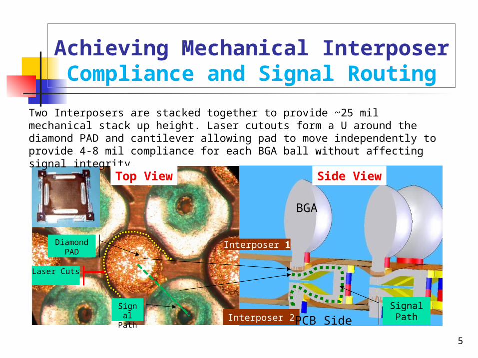
Achieving Mechanical InterposerCompliance and Signal Routing
Two Interposers are stacked together to provide ~25 mil mechanical stack up height. Laser cutouts form a U around the diamond PAD and cantilever allowing pad to move independently to provide 4-8 mil compliance for each BGA ball without affecting signal integrity.
Side ViewTop View
Laser Cuts
BGA
Interposer 1
Interposer 2Signal Path
Diamond PAD
PCB SideSigna
l Path
5

GCI Pin-less Interposer™ SONNET SPICE Model
100ps rise time simulated time plot driving 100 ohm device through GCI Pin-less interposer™
100 ohm SPICE circuit of a GCI interposer
SONNET simulation of two signals, 100 ohm differentially with grounded pads on either side. The pitch between the two GCI interposer pads is 0.8mm. This model represents the interposer with an IC inserted and makes for a very good match to 30 GHz.
Model was limited to 30 GHz due to scaling accuracy of simulator. Time Domain waveform simulation compares nicely with measured waveforms.
6
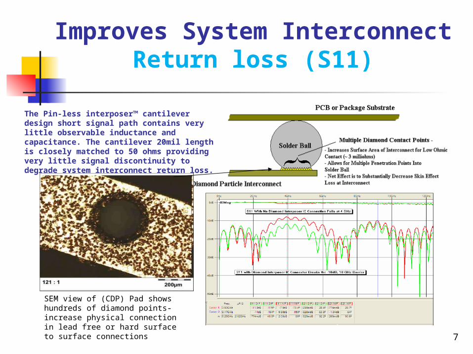
Improves System Interconnect Return loss (S11)
The Pin-less interposer™ cantilever design short signal path contains very little observable inductance and capacitance. The cantilever 20mil length is closely matched to 50 ohms providing very little signal discontinuity to degrade system interconnect return loss.
SEM view of (CDP) Pad shows hundreds of diamond points- increase physical connection in lead free or hard surface to surface connections 7
Conductive Diamond pin-less interposer™ Socket= 98.6 ohms
Typical RF Pogo Pin Socket= 62.2 ohms
Open TDR, No Socket
Internal on-chipTerminated to 100 ohms
Package
100 ohm reference
The Conductive Diamond Pin-less Interpose™ is a better match for the PCB and the transceiver IC onboard terminator. Most significantly, the CDP shows no capacitive or inductive reactance measured to 10gbit. With a uniform impedance profile, the Pin-Less Interposer™ improves the interconnect system Return Loss. A typical Pogo Pin interposer show a 40% impedance error.
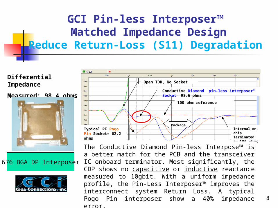
GCI Pin-less Interposer™ Matched Impedance Design
Reduce Return-Loss (S11) Degradation
Differential Impedance
Measured: 98.4 ohms
676 BGA DP Interposer
8
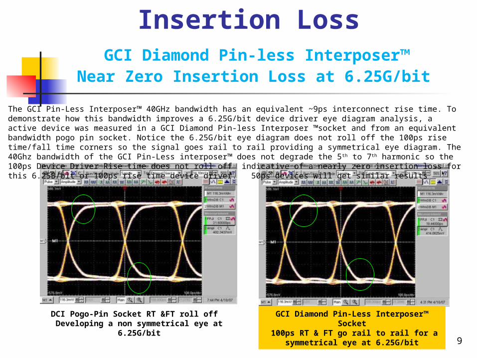
Insertion Loss GCI Diamond Pin-less Interposer™
Near Zero Insertion Loss at 6.25G/bit
DCI Pogo-Pin Socket RT &FT roll off Developing a non symmetrical eye at
6.25G/bit
GCI Diamond Pin-Less Interposer™ Socket
100ps RT & FT go rail to rail for a symmetrical eye at 6.25G/bit
The GCI Pin-Less Interposer™ 40GHz bandwidth has an equivalent ~9ps interconnect rise time. To demonstrate how this bandwidth improves a 6.25G/bit device driver eye diagram analysis, a active device was measured in a GCI Diamond Pin-less Interposer ™socket and from an equivalent bandwidth pogo pin socket. Notice the 6.25G/bit eye diagram does not roll off the 100ps rise time/fall time corners so the signal goes rail to rail providing a symmetrical eye diagram. The 40Ghz bandwidth of the GCI Pin-Less interposer™ does not degrade the 5 th to 7th harmonic so the 100ps Device Driver Rise time does not roll off indicative of a nearly zero insertion loss for this 6.25B/bit or 100ps rise time device driver. 50ps devices will get similar results
9
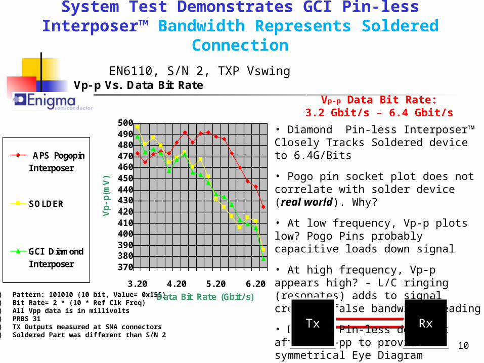
System Test Demonstrates GCI Pin-less Interposer™ Bandwidth Represents Soldered
Connection
1) Pattern: 101010 (10 bit, Value= 0x155)2) Bit Rate= 2 * (10 * Ref Clk Freq)3) All Vpp data is in millivolts4) PRBS 315) TX Outputs measured at SMA connectors6) Soldered Part was different than S/N 2
Vp- p Vs. Data Bit Rate
370380390400410420430440450460470480490500
3.20 4.20 5.20 6.20
Data Bit Rate (Gbit/ s)
Vp-
p(m
V)
APS PogopinInterposer
SOLDER
GCI DiamondInterposer
EN6110, S/N 2, TXP Vswing
RxRx
Vp-p Data Bit Rate:3.2 Gbit/s – 6.4 Gbit/s
• Diamond Pin-less Interposer™ Closely Tracks Soldered device to 6.4G/Bits
• Pogo pin socket plot does not correlate with solder device (real world). Why?
• At low frequency, Vp-p plots low? Pogo Pins probably capacitive loads down signal
• At high frequency, Vp-p appears high? - L/C ringing (resonates) adds to signal creating false bandwidth reading
• Diamond Pin-less does not affect V –pp to provide symmetrical Eye Diagram
TxTx
10
Applications for GCI Pin-Less
Interposers™
11
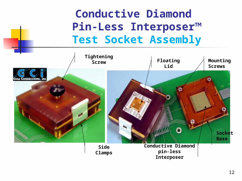
Conductive Diamond Pin-Less Interposer™ Test Socket Assembly
Floating Lid
Conductive Diamond pin-less
Interposer
MountingScrews
Tightening Screw
Side Clamps
Socket Base
12

Manual Device TestingExample: 6-10G/bit
Arm Processor Socket
Quick Release Screw Top
Interposer showing Cantilevers under Kapton interposer
13

QFN Manual Test Sockets 0.5 mm
pitch
14
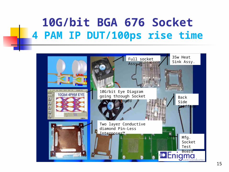
10G/bit BGA 676 Socket4 PAM IP DUT/100ps rise time
Mfg. Socket Test Board
35w Heat Sink Assy.
Back Side Stiffener
Two layer Conductive diamond Pin-Less Interposer™
Full socket Assy.
10G/bit Eye Diagram going through Socket and test board
15

Low Cost OEM Manufacturing
Socket
Same Performance, Simpler Design, Volume OEM Socket
PCB
(Optional) Heat Sink
(Optional) Fan Assembly
Heat Sink Socket
Final Heat Sink Socket Assembly With Fan Mounted On OEM Printed Circuit Board
40 GHz/14psGCI Pin-Less Interposer™Device Package
(Xilinx Vertex5 1150 BGA)
16
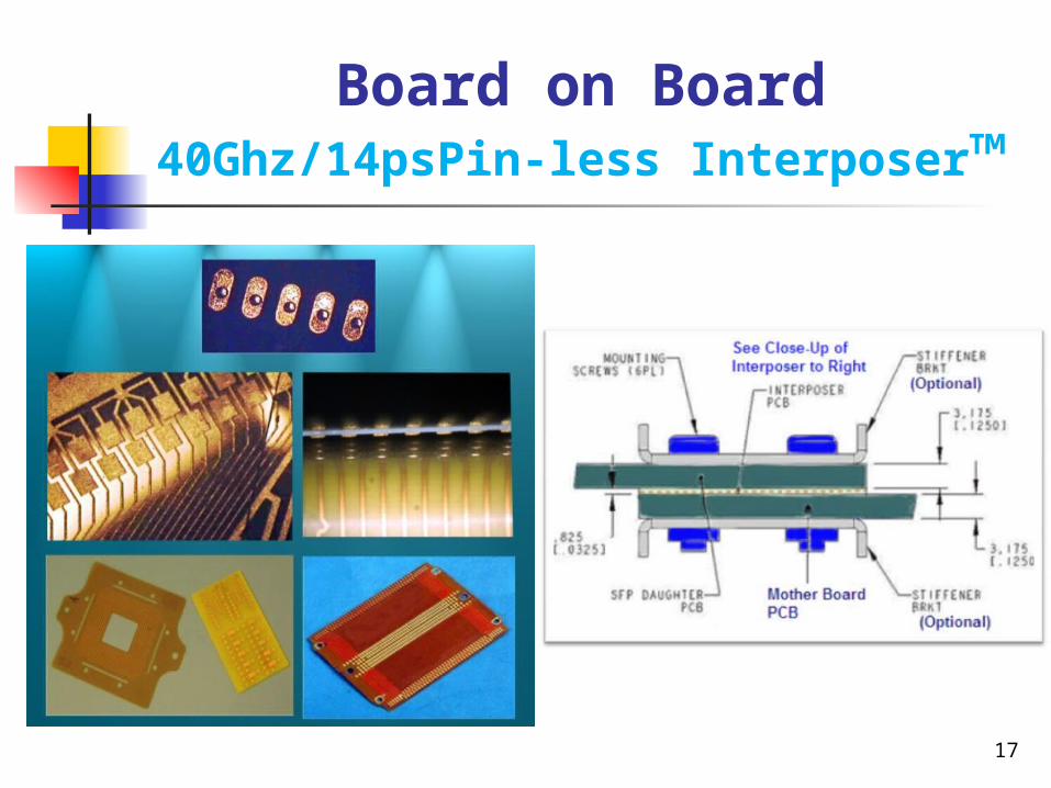
Board on Board40Ghz/14psPin-less Interposer™
17
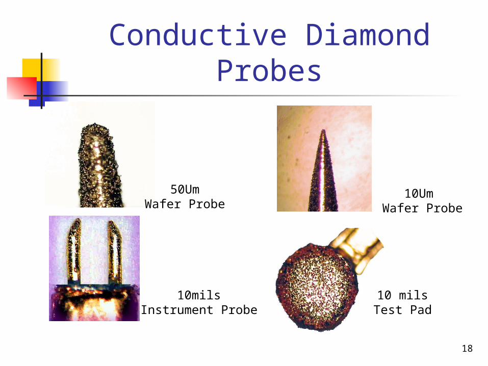
Conductive Diamond Probes
18
50UmWafer Probe
10Um Wafer Probe
10milsInstrument Probe
10 milsTest Pad

For More Information
Company: Giga Connection, Inc. www.gigaconnections.com Sales:
Brian Shumaker [email protected] Ph 650 593-7083
19