Xilinx CPLDs and FPGAs Lecture L1.1. CPLDs and FPGAs XC9500 CPLD Spartan II FPGA Virtex FPGA.
Getting Started with ReconfigurableLogic
(CPLDs and FPGAs)Prepared By Dr. Hossam Eldin Mostafa
Alexandria University, Faculty of Engineering, Alexandria, Egyptwww.cs.ucf.edu/~ahossam/
Main
CPLD Starter Kit
Hardware
Software
Examples
DocumentationBlock diagram of XC9500 series
Pin diagrams XC9536-PC44XC9536 Datasheet
PLCC Socket
This page is last updated on 1st December 2003

Getting Started with ReconfigurableLogic
(CPLDs and FPGAs)
What is CPLD
A lot of logic devices are housed in CPLD and those connections can be specified by the program. For example, in case of the 7400 IC, 4 circuitsof 2 input NAND gate are housed. In case of 7404, 6 circuits of inverter are housed. These are separate IC. Therefore, to compose a circuit, it isnecessary to do each wiring among the pins using the printed board. In case of CPLD, it has wiring among the logic in the IC. So, the wiring onthe printed board can be made little.
The capacity of CPLD is limited. There is limitation on the number of the pins, too. So, don't do excessive expectations. The outlinespecification of the part of the XC9500 series of Xilinx Inc. is shown below.
6FB/108macrocells/2400gates 84pin PLCC XC95108-15PC84C 4FB/72macrocells/1600gates 84pin PLCC XC9572-15PC84C 4FB/72macrocells/1600gates 44pin PLCC XC9572-15PC44C 2FB/36macrocells/800gates 44pin PLCC XC9536-15PC44C
SpecificationNumber of pins Parts name

The point which CPLD is convenient for is the thing about which it is possible to rewrite many time because it is recording thecontents of the circuit to the flash memory. In the XC9500 series, rewriting in about 10,000 times is said to be possible. Also, becausethe pin for the rewriting is preparatory, the contents can be rewritten in the condition to have mounted to the actual circuit if there iswiring (In Circuit Programming).
Complex Programmable Logic Devices (CPLD) are another way to extend the density of the simple PLDs. The concept is to have afew PLD blocks or macrocells on a single device with general purpose interconnect in between. Simple logic paths can beimplemented within a single block. More sophisticated logic will require multiple blocks and use the general purpose interconnect inbetween to make these connections.
CPLDs are great at handling wide and complex gating at speeds e.g. 5ns which is equivalent to 200MHz. The timing model forCPLDs is easy to calculate so before you even start your design you can calculate your in to output speeds.
Why use a CPLD1- Ease of Design:
CPLDs offer the simplest way to implement design. Once a design has been described, by schematic and/or HDL entry, a designersimply uses CPLD development tools to optimise, fit, and simulate the design. The development tools create a file, which is then usedto customise (program) a standard off-the-shelf CPLD with the desired functionality. This provides an instant hardware prototype andallows the debugging process to begin. If modifications are needed, design changes are just entered into the CPLD development tool,and the design can be re-implemented and tested immediately.
2- Lower Development Costs:
CPLDs offer very low development costs. Ease of design, as described above, allows for shorter development cycles. Because CPLDsare re-programmable, designers can easily and very inexpensively change their designs. This allows them to optimise their designsand continues to add new features to continue to enhance their products. CPLD development tools are relatively inexpensive and inthe case of Xilinx, are free. Traditionally, designers have had to face large cost penalties such as re-work, scrap, and developmenttime. With CPLDs, designers have flexible solutions thus avoiding many traditional design pitfalls.
3- More Product Revenue:
CPLDs offer very short development cycles, which means your products get to market quicker and begin generating revenuesooner. Because CPLDs are re-programmable, products can be easily modified using ISP over the Internet. This in turn allows you toeasily introduce additional features and quickly generate new revenue from them. (This results in an expanded time for revenue).Thousands of designers are already using CPLDs to get to market quicker and then stay in the market longer by continuing toenhance their products even after they have beenintroduced into the field. CPLDs decrease Time To Market (TTM) and extend Time In Market (TIM).
4- Reduced Board Area:
CPLDs offer a high level of integration (large number of system gates per area) and are available in very small form factor packages.This provides the perfect solution for designers of products which must fit into small enclosures or who have a limited amount ofcircuit board space to implement the logic design. The CoolRunner? CPLDs are available in the latest chip scale packages, e.g. CP56which has a pin pitch of 0.5mm and is a mere 6mm by 6mm in size so are ideal for small, low power end products.
5- Cost of Ownership:
Cost of Ownership can be defined as the amount it costs to maintain, fix, or warranty a product. For instance, if a design changerequiring hardware rework must be made to a few prototypes, the cost might be relatively small. However, as the number of unitsthat must be changed increases, the cost can become enormous. Because CPLDs are re-programmable, requiring no hardwarerework, it costs much less to make changes to designs implemented using them. Therefore cost of ownership is dramaticallyreduced. And don't forget the ease or difficulty of design changes can also affect opportunity costs. Engineers who are spending a lotof time fixing old designs could be working on introducing new products and features - ahead of the competition. There are alsocosts associated with inventory and reliability. PLDs can reduce inventory costs by replacing standard discrete logic devices.Standard logic has a predefined function and in a typical design lots of different types have to be purchased and stocked. If thedesign is changed then there may be excess stock of superfluous devices. This issue can be alleviated by using PLDs i.e. you onlyneed to stock one device and if your design changes you simply reprogram. By utilising one device instead of many your boardreliability will increase by only picking and placing one device instead of many. Reliability can also be increased by using the ultralow power CoolRunner CPLDs i.e. lower heat dissipation and lower power operation leads to decreased Failures In Time (FIT).
In 1985, a company called Xilinx introduced a completely new idea. The concept was to combine the user control and time to marketof PLDs with the densities and cost benefits of gate arrays. A lot of customers liked it - and the FPGA was born. Today Xilinx is stillthe number one FPGA vendor in the world! An FPGA is a regular structure of logic cells? or modules and interconnect which isunder the designer’s complete control. This means the user can design, program and make changes to his circuit whenever hewants. And with FPGAs now exceeding the 10 million gate limit (Xilinx Virtex? II is the current record holder), the designer candream big!

CPLD Starter Kit
What is includedThe components listed in the following table are included with the starter kit (The images of the components are shown in theabove image)
Download the above table in PDF format (kit_components.pdf) or in Exel format (kit_components.xls)
What is NOT included

The following components are NOT included with the starter kit.
1- +5v Power Supply
2- Parallel Port Adaptor
OR Parallel Port Male Connector
4- DB25 Male -Female Cable
5- Bread Boards
6- Connecting Wires
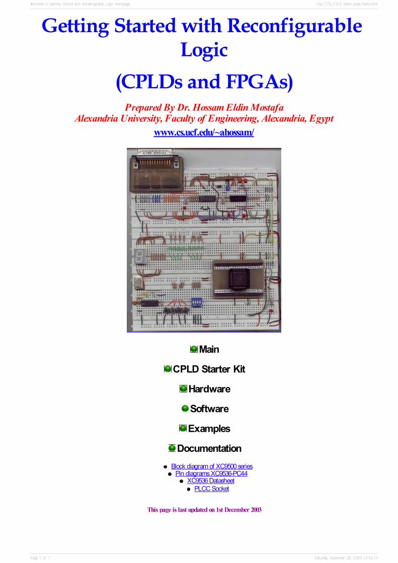
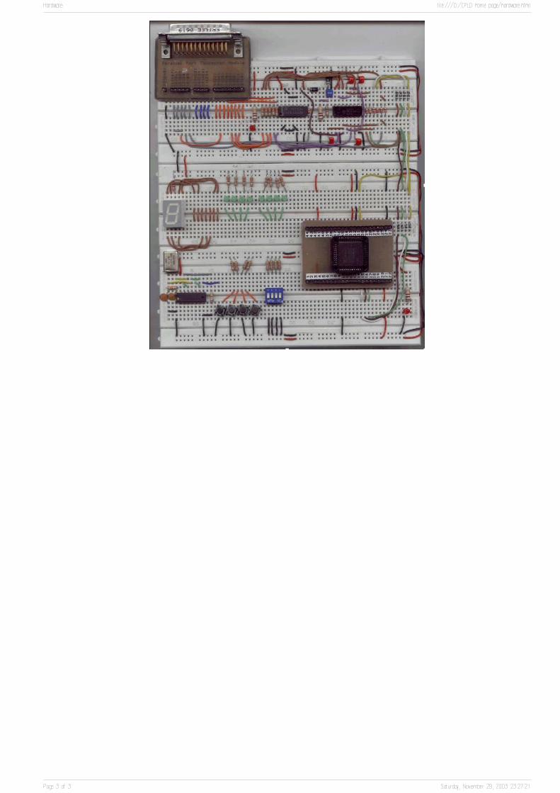
HARDWARE
JTAG Parallel Port Programmer
To download the the schematic in PDF format click here jtag.pdf
(All the components are included with the starter kit)
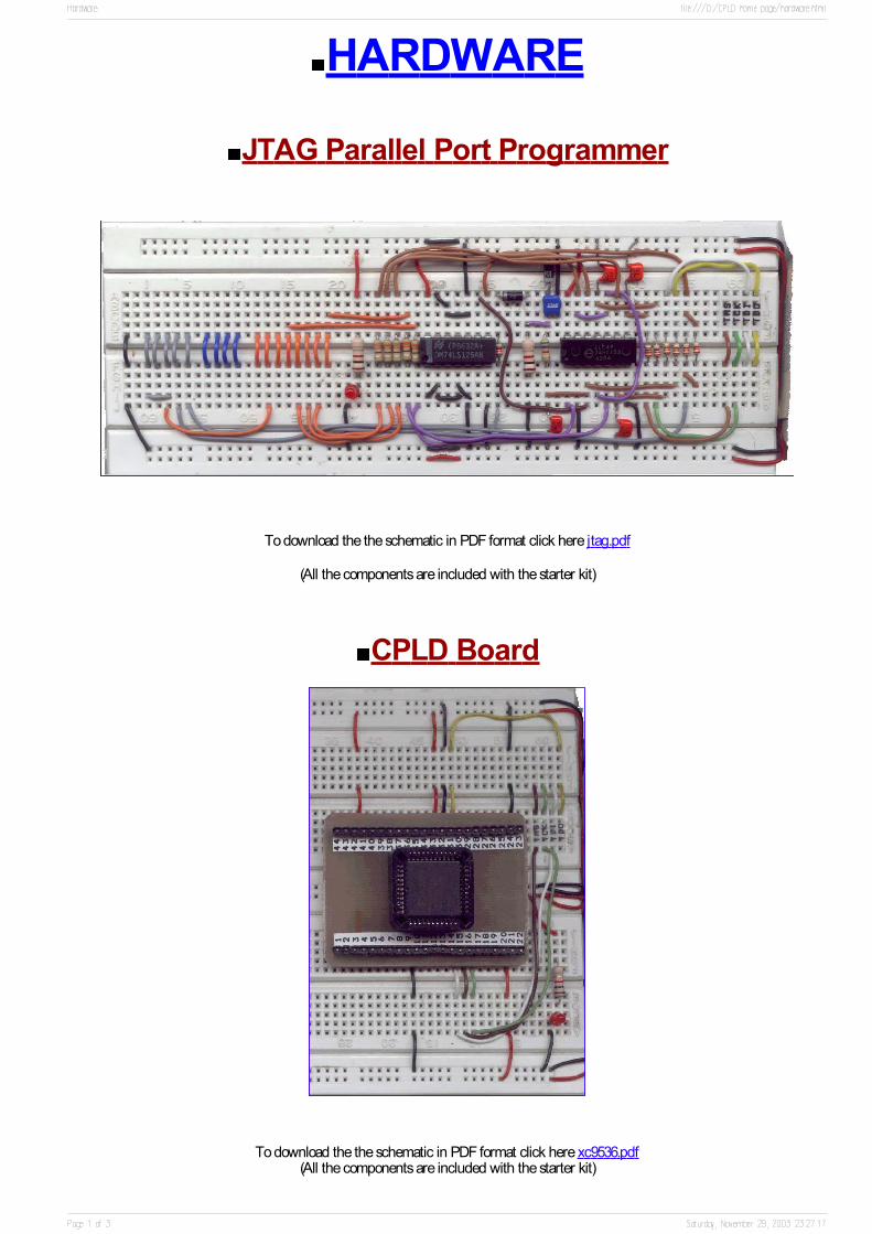
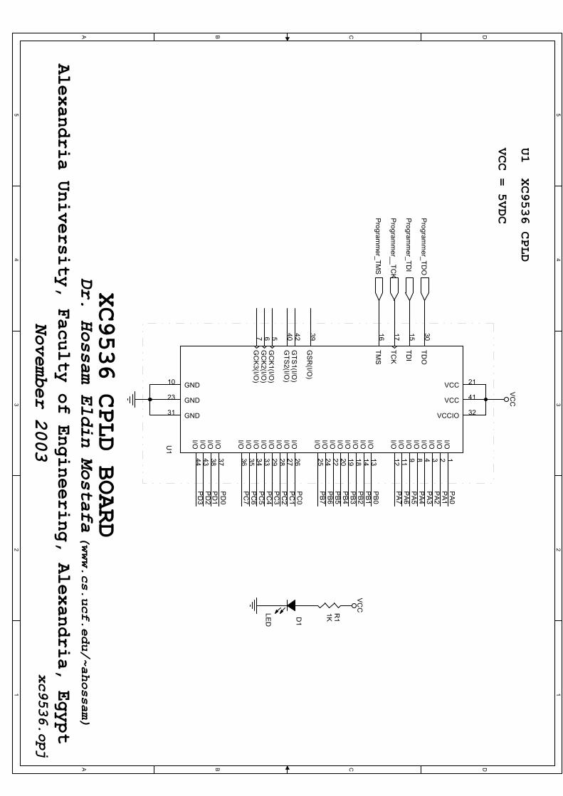
CPLD Board
To download the the schematic in PDF format click here xc9536.pdf(All the components are included with the starter kit)
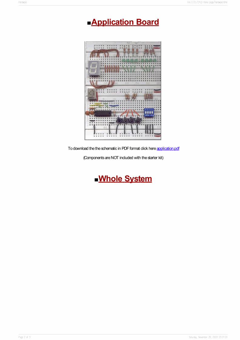
Application Board
To download the the schematic in PDF format click here application.pdf
(Components are NOT included with the starter kit)
Whole System

55
44
33
22
11
DD
CC
BB
AA
CPLD
HEADER
FPGA
HEADER
DB-25 PARALLEL PORT CONNECTOR
Notes:
U1 74LS125
U2 74HC125
U1 and U2 power:GND pin 7
VCC pin14
Xilinx CPLD & FPGA Parallel Port Programmer
Dr. Hossam Eldin MostafaAlexandria University, Faculty of Engineering, Alexandria, Egypt
November 2003jtag.opj
(www.cs.ucf.edu/~ahossam)
VCC SENSE
PROG
CLK
DIN
TMS_IN
DONE
CTRL
R11K
R35.6K
R4
120
R5
120R6
120
D1
1N4004
D2
1N4004
U1C 9
8
10
C1
22n
C2
100p
C3
100p
U2B
56
4
U5D
1211
13U2C
98
10
R7
120
R21K
U2A
23
1
R14
330
R9
120
R10
120
U1B
56
4
U1D
1211
13
R12
330
U1A
23
1
R8
120
R11
330
C4
100p
C5100p
R13
330
R15
330
D3LED
VCC
GND
TDO
TDI
TCK
TMS
D/P
DIN
VCC
GND
CCLK
*PROG
13(S4)
15(S3)
3(D1)
4(D2)
6(D4)
2(D0)
5(D3)
8(D6)
11(*S7)
12(S6)
25(GND)
55
44
33
22
11
DD
CC
BB
AA
U1 XC9536 CPLDVCC = 5VDC
xc9536.opj
(www.cs.ucf.edu/~ahossam)Dr. Hossam Eldin MostafaXC9536 CPLD BOARD
November 2003Alexandria University, Faculty of Engineering, Alexandria, Egypt
PA0PA1
PA4PA5
PB0PB1PB2PB3PB4PB5PB6PB7
PC0
PC1
PC2
PC3
PC4
PC5
PC6
PC7
PD0
PD1
PD2
PD3
PA7PA6
PA3PA2
VCC
VCC
R11K
U1
32
41
21
123489111213141819
17
10
23
31
2022262728293334 2425353637384344
30394240567 1516
VCCIO
VCC
VCC
I/OI/OI/OI/OI/OI/OI/OI/OI/OI/OI/OI/O
TCK
GND
GND
GND
I/OI/OI/OI/OI/OI/OI/OI/O I/OI/OI/OI/OI/OI/OI/OI/O
TDO
GSR(I/O
)
GTS1(I/O
)GTS2(I/O
)
GCK1(I/O
)GCK2(I/O
)GCK3(I/O
)
TDI
TMS
D1
LED
Programmer_TD
O
Programmer_TD
I
Programmer__TC
K
Programmer_TM
S

55
44
33
22
11
DD
CC
BB
AA
PUSH BUTTONS MODULEDIP SWITCHES MODULE
CLOCK GENERATOR MODULE
7 SEGMENT MODULE
b
cgd
a
e
f
LED MODULE
APPLICATION BOARD
November 2003
Dr. Hossam Eldin MostafaAlexandria University, Faculty of Engineering, Alexandria, Egypt
application.opj
(www.cs.ucf.edu/~ahossam)
S2S1
S0P3
L0
P1P0
L3
P2S3
L1L2
CLK_OUT
dg
ec
fba
L4L5
L6L7
VCC
VCC
VCC
VCC
VCC
R13
10K
R5
330
D1
LED
D2
LED
D3
LED
D4
LED
R16
10K
R1
330R
7330
R15
10KR
1410K
U1D
121311
D6
LED
R2
330
U1C
9108
147
R9
330
R3
330
D8
LED
R4
330
D7
LED
R6
330
SW
1
SW D
IP-4
1234
8765
D5
LED
R8
330
R17
10K
D9
LED
C1
33p
R20
1K
C2
33p
R19
6.8k
R10
10K
Y112M
R11
10K
R18
3.3K
R12
10K

XILINX WebPACK TutorialPrepared by Dr. Hossam Eldin Mostafa
Faculty of Engineering, Alexandria University, Alexandria, Egypt.
(www.cs.ucf.edu/~ahossam/)
The Xilinx Inc. is providing the software tools to design CPLDs and FPGAs.This software is called WebPACK.WebPACK is available free-of-charge by registering. You can download them from the XILINX site www.xilinx.com.
As for the WebPACK tool, a new type is released in order. Therefore, the operation is may be a little bit different from the tool whichis introduced on this webpage.
This section is a step by step approach to your first simple design. The following pages are intended to demonstrate the basic PLDdesign entry and implementation process. In this example tutorial a simple HEX to seven segment decoder is designed in VHDL.The design is initially targeted at a XC9536 CPLD.
Example Project
In this example(see the left image), we will design a Hex to seven segment decoder. The circuit accepts 4 binary bits as inputs (I3 I2 I1I0) and produces 7 binary bits as outputs (O6 O5 O4 O3 O2 O1 O0). It is directed to derive a common anode seven segment display.The right image shows the test circuit for this design using XC9536, DIP switches modules to generate the inputs and the sevensegment module to see the outputs. The pin out os the CPLD is illustrated and will be defined in the VHDL program. You candownload the above image in PDF format from decoder.pdf
The VHDL file that will be writtrn can be downloaded here decoder.vhd.
The whole Webpack project can be downloaded from here decoder.zip
Developing the project using WebPACK
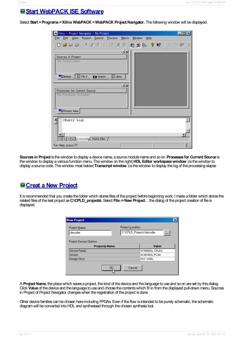
Start WebPACK ISE SoftwareSelect Start > Programs > Xilinx WebPACK > WebPACK Project Navigator. The following window will be displayed.
Sources in Project is the window to display a device name, a source module name and so on. Processes for Current Source isthe window to display a various function menu. The window on the right( HDL Editor workspace window ) is the window todisplay a source code. The window most below( Transcript window ) is the window to display the log of the processing elapse
Creat a New ProjectIt is recommended that you create the folder which stores files of the project before beginning work. I made a folder which stores therelated files of the test project as C:\CPLD_projects\. Select File -> New Project… the dialog of the project creation of file isdisplayed.
A Project Name, the place which saves a project, the kind of the device and the language to use and so on are set by this dialog.Click Value of the device and the language to use and choose the contents which fit in from the displayed pull-down menu. Sourcesin Project of Project Navigator changes when the registration of the project is done.
Other device families can be chosen here including FPGAs. Even if the flow is intended to be purely schematic, the schematicdiagram will be converted into HDL and synthesised through the chosen synthesis tool.
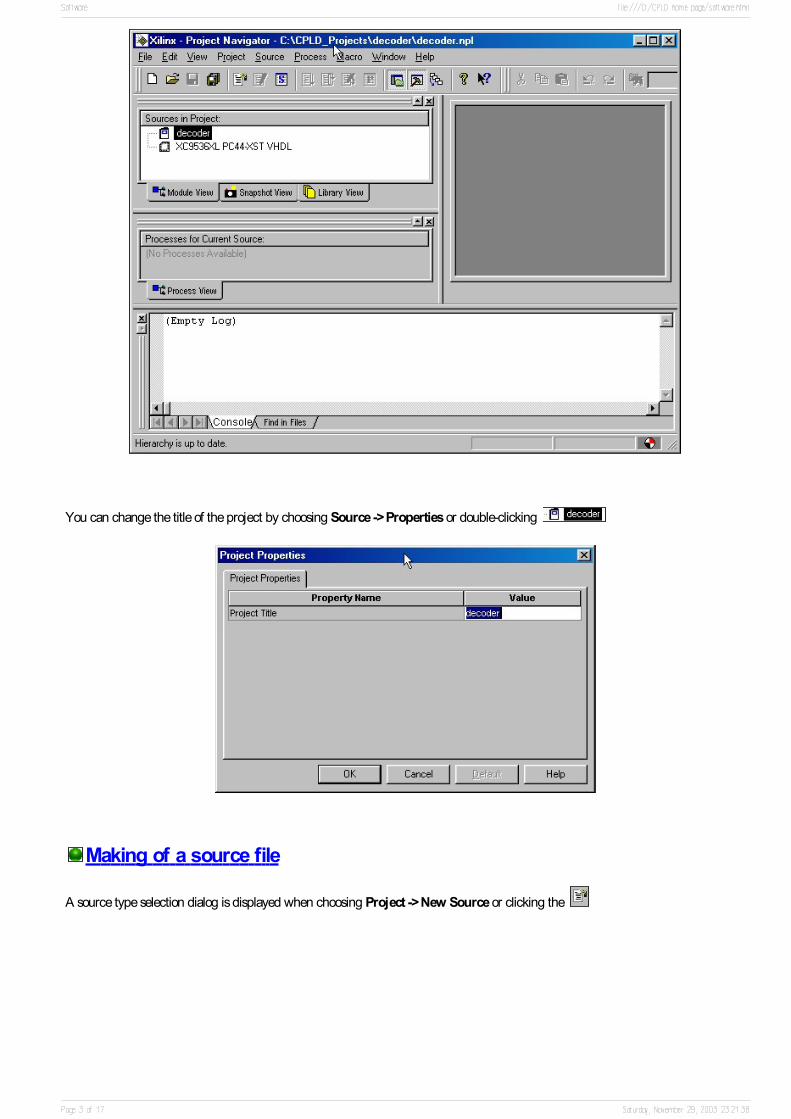
You can change the title of the project by choosing Source -> Properties or double-clicking
Making of a source file
A source type selection dialog is displayed when choosing Project -> New Source or clicking the

Select "VHDL Module" from the displayed item. When using a language except VHDL, select a corresponding language. Type "FileName", and confirm the file saving path of "Location" and click "Next".
Type "Entity Name" and "Architecture Name". The ports can be specified by this dialog. However, in this example we specifiethem by the description of VHDL from behind. Click "Next" without assigning the ports. This table automatically generates the entityin the decoder VHDL module. Following confirmation screen is displayed. Click "Finish" if there is not mistake in the contents.

The window (HDL Editor window) of the source code is displayed in HDL Editor workspace window of Project Navigator
Display or non-display of each window can be controlled with the View menu.To spread a source code window, click Project Workspace of the View menu and removes checking. You can expand by clicking
, too. To make display a source code window in whole HDL Editor workspace window, click the window maximizationbutton in the upper right like usual window control. The basic part of the format of VHDL is already written in the displayed sourcecode window.

This time, you adde the following to entity and architecture to implement the decoder.

You can download the VHDL file from decoder.vhd
After doing the above-mentioned change, save a file by File -> Save or by the button. The attribute keyword is used to definethe input and output pins of the CPLD inside the VHDL file.
Syntax checkBy the following operation, the grammar of the made source file is confirmed. Double-click "Check Syntax" which is displayed in theProcess for Current Source window. This has the checking of format (Syntax). If the checking result is to be OK, Check Syntaxhas a green checking mark. Also, "Done: completed successfully." is displayed in the end of the situation display window.
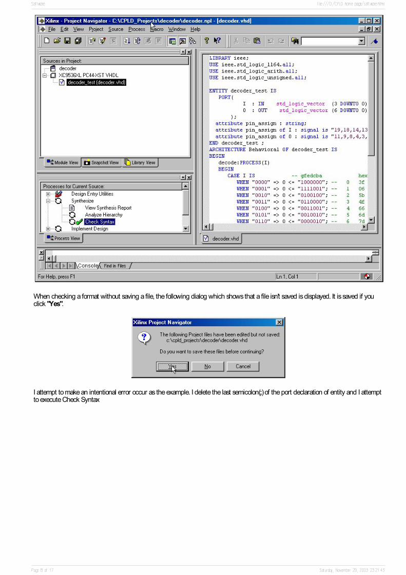
When checking a format without saving a file, the following dialog which shows that a file isn't saved is displayed. It is saved if youclick "Yes".
I attempt to make an intentional error occur as the example. I delete the last semicolon(;) of the port declaration of entity and I attemptto execute Check Syntax

Check Syntax has a red X mark. Also, "Done: failed with exit code: 0001." is displayed in the end of the situation display window.The position of the error can be known with the situation display window.
ERROR : (VHP__0162). C:\CPLD_projects\decoder\decodr.vhd Line 11. Read symbol ATTRIBUTE, expecting ';'.An error is detected at the 11th line. When double-clicking , the mark which shows an error on the left side of the source code isdisplayed. Because the mark shows the line which detected an error. So, check previous lines and so on.

Fittingthe file which will be written to the CPLD is generated fron the VHDL file using this process. Double-click "Fitter" which is displayedat the Process for Current Source window. The fitting processing begins with this operation.

Fit Design has a green checking mark if the fitting result is to be OK. Also, "Done: completed successfully" is displayed in the endof the situation display window.
The Confirmation of the Fitting ResultIn case of complicated circuits, the various data must be confirmed. This time, we confirm the situation of the assigned pin.Double-click Fitter Report which is displayed in the Process for Current Source window. A report window is displayed. There isfollowing figure in it. This figure shows the assignment of the pins.
If we did not predefine the inputs and output pins (using the attribute keyword), the tool will selecting pins automatically. So, thedesign may not look neat.
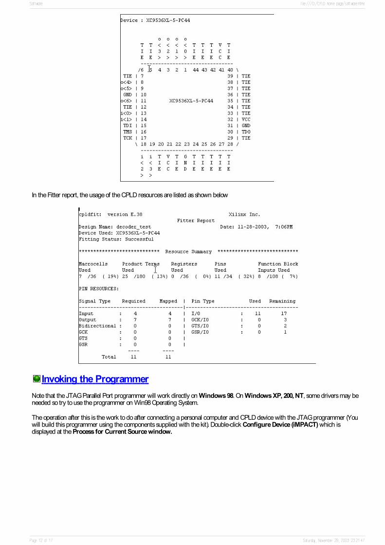
In the Fitter report, the usage of the CPLD resources are listed as shown below
Invoking the ProgrammerNote that the JTAG Parallel Port programmer will work directly on Windows 98. On Windows XP, 200, NT, some drivers may beneeded so try to use the programmer on Win98 Operating System.
The operation after this is the work to do after connecting a personal computer and CPLD device with the JTAG programmer (Youwill build this programmer using the components supplied with the kit). Double-click Configure Device (iMPACT) which isdisplayed at the Process for Current Source window.

The window of JTAG Programmer is shown below.
When using the parallel port of the PC, it specifies Parallel by Output -> Cable Setup -> Cable Communication Setup. Data istransferred to CPLD if pushing the OK button. When a cable isn't connected, it becomes an error.
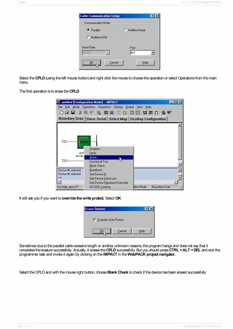
Select the CPLD (using the left mouse button) and right click the mouse to choose the operation or select Operations from the mainmenu
The first operation is to erase the CPLD
It will ask you if you want to override the write protect. Select OK
Sometimes due to the parallel cable exessive length or another unknown reasons, the program hangs and does not say that itcompletes the erasure successfully. Actually, it erases the CPLD successfully. But you should press CTRL + ALT + DEL and end theprogrammer task and invoks it again by clicking on the iMPACT in the WebPACK project navigator.
Select the CPLD and with the mouse right button, choose Blank Check to check if the device has been erased successfully
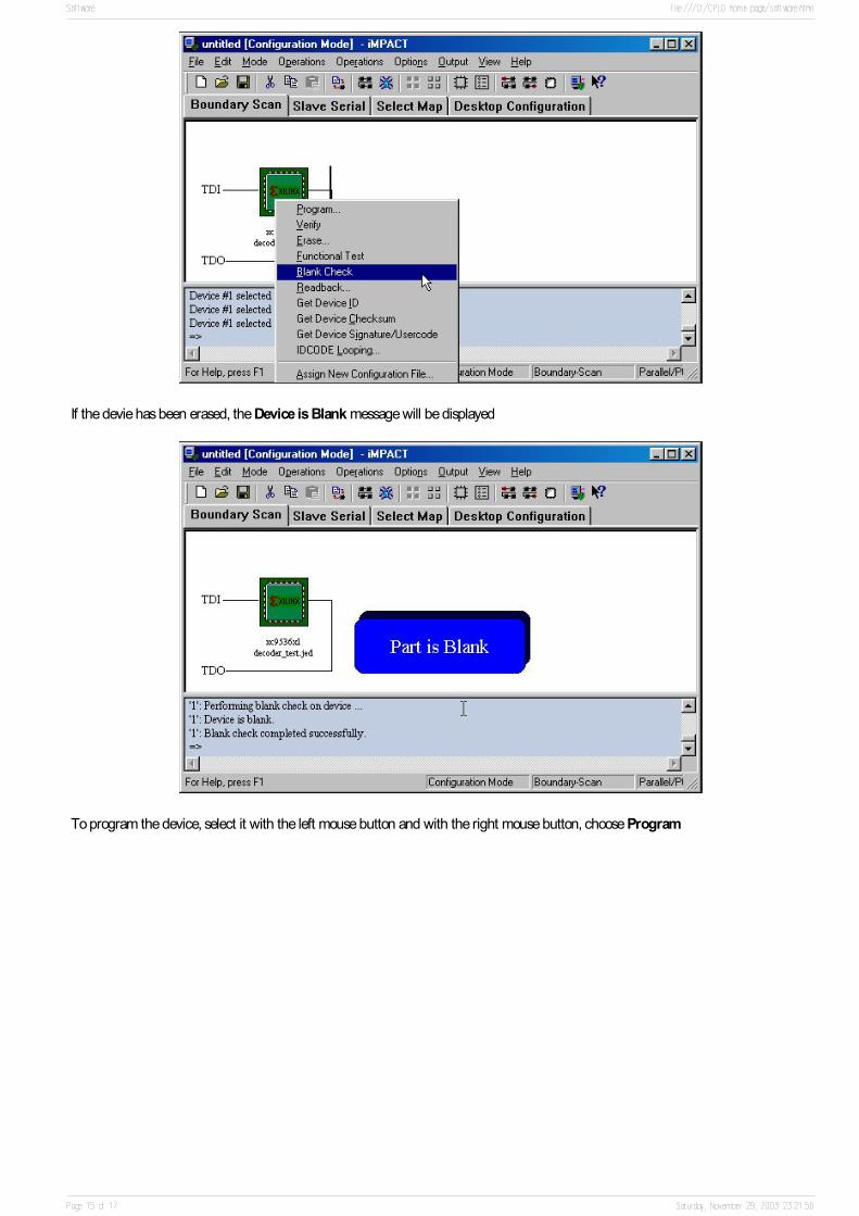
If the devie has been erased, the Device is Blank message will be displayed
To program the device, select it with the left mouse button and with the right mouse button, choose Program
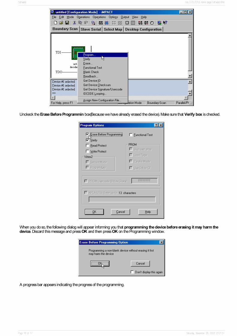
Unckeck the Erase Before Programmin box(Because we have already erased the device). Make sure that Verify box is checked.
When you do so, the following dialog will appear informing you that programming the device before erasing it may harm thedevice. Discard this message and press OK and then press OK on the Programming window.
A progress bar appears indicating the progress of the programming.

When programming is OK, a Programming Succeded message appears.
Now, you can try the program you have just downloaded if you connect the CPLD inputs to the DIP switched and the CPLD outputsto the seven segment,

Block diagram of XC9500 series
You can jump to the page of the explanation when you click the part where the pointer become the hand.
If you want to know more detailed specification, refer to the following PFD file.
I/O Blocks
An I/O block is composed of input buffer, output buffer,multiplexer for the output control and grounding control and so on.Multiplexer for the output control(OE MUX) controls an outputenable or stop. It is controlled by the signal from the macrocell or thesignal of the GTS(Global Three-State control) pin. It can alwaysmake output '1' or '0', too. There are four GTS in XC95216 andXC95288 and in case of the other device, they are two.A slew rate control is the one to make the rising and the falling ofthe output pulse smooth. It is used when suppressing the occurrenceof the noise.A grounding control is used when making input/output pin (I/O)an earth terminal. In case of the circuit where much noise occurs, itisn't sometimes possible to do noise reducing by the standard earthterminal.At the actual circuit, a pull-up resistor is more connected with theinput/output pin. This circuit makes an input/output pin '1'condition compulsorily during programming of CPLD to make aninfluence by the condition of the I/O pin little. This circuit is detachedin usualoperation

in usual operation.
Each input/output pin can handle a 24-mA current.
FastCONNECT Switch Matrix
FastCONNECT Switch Matrix controls the input signals to theFunction Block.All the signals from the input-output port and the signals of theFunction Block are connected with FastCONNECT SwitchMatrix. The signals which are specified by the program out ofthese signals are applied to the Function Block. The outputsignals from the Function Block are applied to the FunctionBlock through the wired AND buffer. This provides additionallogic capability and increases the effective logic fan-in of thedestination Function Block without any additional timing delay.It is automatically invoked by the development software whereapplicable.
Function Block
Function block is composed of the programmable ANDarray, product term allocator and macrocell.
36 pieces of signals inputted to the Function Block aredivided into the true and complement signals by theprogrammable AND array and become 72 kinds ofsignals.In Product Term Allocator, it applys the signal withcombination of them to the macrocell.A macrocell is composed of one D/T type flip-flop. Thesignals of set/reset/clock to this flip-flop are supplied bythe Product Term Allocator.The output of the logic circuit can be connected with thepin without using a flip-flop, too.
There are 18 independent macrocells in one FunctionBlock.There are 18 pieces of output in the Function Block andthey are connected with FastCONNECT Switch Matrixand I/O blocks. Also, the set/reset signal(GSR : GlobalSet/Reset) and the clock signal(GCK : Global Clocks) areinputted to the Function Block and are used for thecondition of the operation of the flip-flop according to
need.
PTOE(Product Term Output Enable) signal is output to I/O block from Product Term Allocator.
The number of the Function Blocks depends on the device. As for XC9536, 2 blocks are mounted, as for XC9572, 4 blocks are mounted and as for XC95108, 6blocks are mounted.It isn't sometimes possible to use all macrocells by the limitation on the number of the pins. For details, confirm pin diagrams. There are few cases which connect allmacrocells with the pin actually. Generally, there are macrocells to use only in the logic inside.

In-System Programming
XC9500 devices are programmed in-system via a standard 4-pinJTAG(Joint Test Action Group) protocol. The devices fully supportIEEE 1149.1 boundary-scan(JTAG).Because it is equipped with the pin for independent JTAG, theprogram can be changed as it mounted CPLD on the printedboard.
While programing, all input ports in the I/O block are set to the 'H'level.
The wires to use in JTAG are the following four. Each use is shownbelow.
Read back data from the target system is read at this pin.
TDO(Read Data):
This signal is used to transmit serial test instructions anddata.
TDI(Test Data In):
This clock drives the test logic for all devices onboundary-scan chain.
TCK(Test Clock):
This signal is decoded by the TAP controller to control testoperations.
TMS(Test Mode Select):

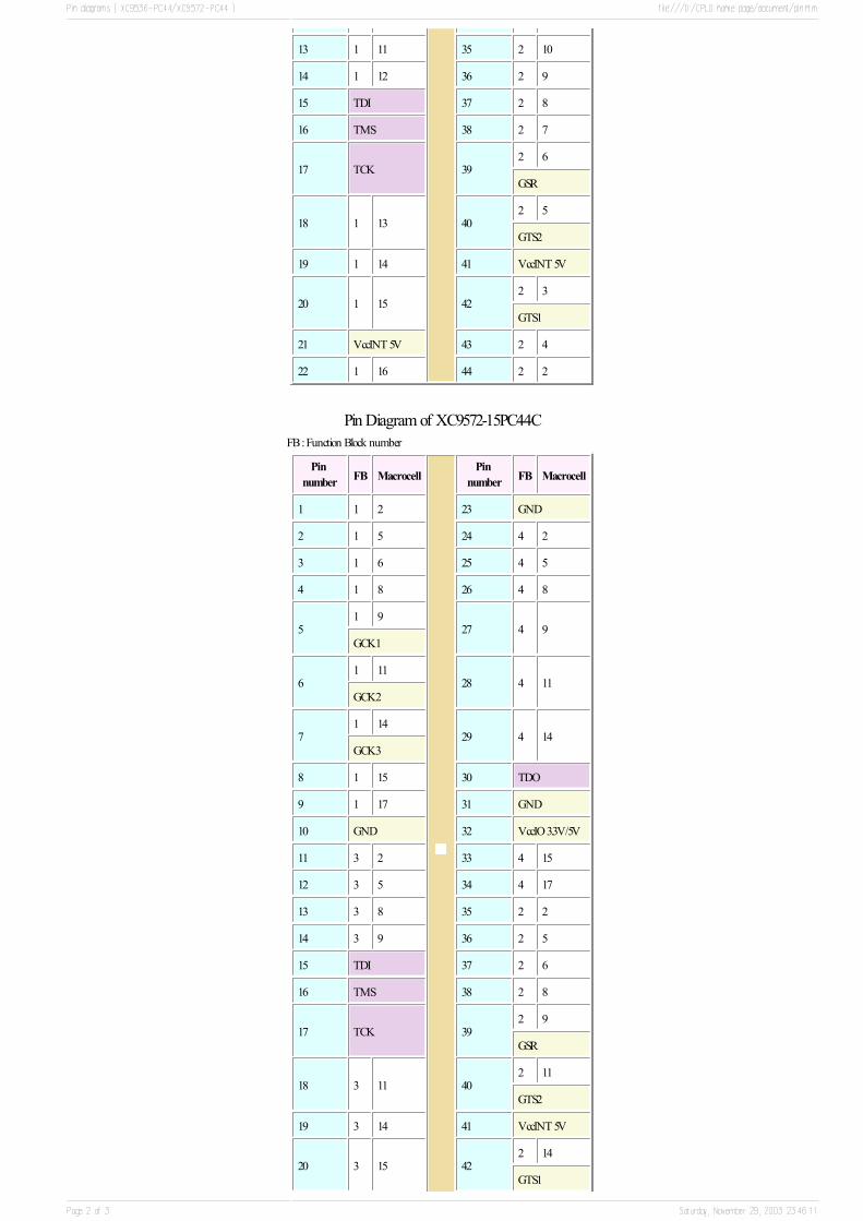
Pin diagrams ( XC9536-PC44/XC9572-PC44 )
The figure on the left is the top view of CPLD of 44 pins.The following item is used to know the position of the pin.
*The direction of the printed name.*A corner in the upper left is shaved.
A pin numbering is counterclockwise given from the center of the line in the topside.
Note is necessary to the pin arrangement by the Function Block and the macrocellbecause it a little irregular-ly.
In case of XC9536-PC44, the macrocells which corresponds to the input/output pins are34 macrocells in the 36 macrocells.In case of XC9572-PC44, they are 34 macrocells in the 72 macrocells.The macrocells which don't correspond to the input/output pins can be used only in thelogic circuits inside.
The pins colored purple are pins for JTAG.
Pin Diagram of XC9536-15PC44CFB : Function Block number
1123410112
122339111
VccIO 3.3V/5V32GND10
GND31819
TDO30618
GCK313229
717
GCK214228
516
GCK115227
315
16226414
17225213
17124112
GND23121
MacrocellFBPinnumberMacrocellFB
Pinnumber
224416122
4243VccINT 5V21
GTS1
324215120
VccINT 5V4114119
GTS2
524013118
GSR
6239TCK17
7238TMS16
8237TDI15
923612114
1023511113
Pin Diagram of XC9572-15PC44CFB : Function Block number
GTS1
1424215320
VccINT 5V4114319
GTS2
1124011318
GSR
9239TCK17
8238TMS16
6237TDI15
52369314
22358313
174345312
154332311
VccIO 3.3V/5V32GND10
GND311719
TDO301518
GCK314429
1417
GCK211428
1116
GCK19427
915
8426814
5425613
2424512
GND23211
MacrocellFBPinnumberMacrocellFB
Pinnumber

1724417322
15243VccINT 5V21

9
Features• 5 ns pin-to-pin logic delays on all pins• fCNT to 100 MHz
• 36 macrocells with 800 usable gates• Up to 34 user I/O pins• 5 V in-system programmable (ISP)
- Endurance of 10,000 program/erase cycles- Program/erase over full commercial voltage and
temperature range• Enhanced pin-locking architecture• Flexible 36V18 Function Block
- 90 product terms drive any or all of 18 macrocells within Function Block
- Global and product term clocks, output enables, set and reset signals
• Extensive IEEE Std 1149.1 boundary-scan (JTAG) support
• Programmable power reduction mode in each macrocell
• Slew rate control on individual outputs• User programmable ground pin capability• Extended pattern security features for design protection• High-drive 24 mA outputs• 3.3 V or 5 V I/O capability• Advanced CMOS 5V FastFLASH technology• Supports parallel programming of more than one
XC9500 concurrently• Available in 44-pin PLCC, 44-pin VQFP, and 48-pin
CSP packages
DescriptionThe XC9536 is a high-performance CPLD providingadvanced in-system programming and test capabilities forgeneral purpose logic integration. It is comprised of two36V18 Function Blocks, providing 800 usable gates withpropagation delays of 5 ns. See Figure 2 for the architec-ture overview.
Power ManagementPower dissipation can be reduced in the XC9536 by config-uring macrocells to standard or low-power modes of opera-tion. Unused macrocells are turned off to minimize powerdissipation.
Operating current for each design can be approximated forspecific operating conditions using the following equation:
ICC (mA) =
MCHP (1.7) + MCLP (0.9) + MC (0.006 mA/MHz) f
Where:
MCHP = Macrocells in high-performance mode
MCLP = Macrocells in low-power mode
MC = Total number of macrocells used
f = Clock frequency (MHz)
Figure 1 shows a typical calculation for the XC9536 device.
1
XC9536 In-System Programmable CPLD
December 4, 1998 (Version 5.0) 1 1* Product Specification
Clock Frequency (MHz)
Typ
ical
I CC
(m
A)
0 50
(50)
(30)
(83)
(50)
100
High Performance
Low Power
X5920
Figure 1: Typical ICC vs. Frequency For XC9536
December 4, 1998 (Version 5.0) 1

XC9536 In-System Programmable CPLD
In-System Programming ControllerJTAGController
I/OBlocks
FunctionBlock 1
Macrocells1 to 18
Macrocells1 to 18
JTAG Port
3
36
I/O/GTS
I/O/GSR
I/O/GCK
I/O
I/O
I/O
I/O
2
1
I/O
I/O
I/O
I/O
3
X5919
1
FunctionBlock 2
36
18
18
Fas
tCO
NN
EC
T S
witc
h M
atrix
Figure 2: XC9536 Architecture
Note: Function Block outputs (indicated by the bold line) drive the I/O Blocks directly
2 December 4, 1998 (Version 5.0)
XC9536 In-System Programmable CPLD
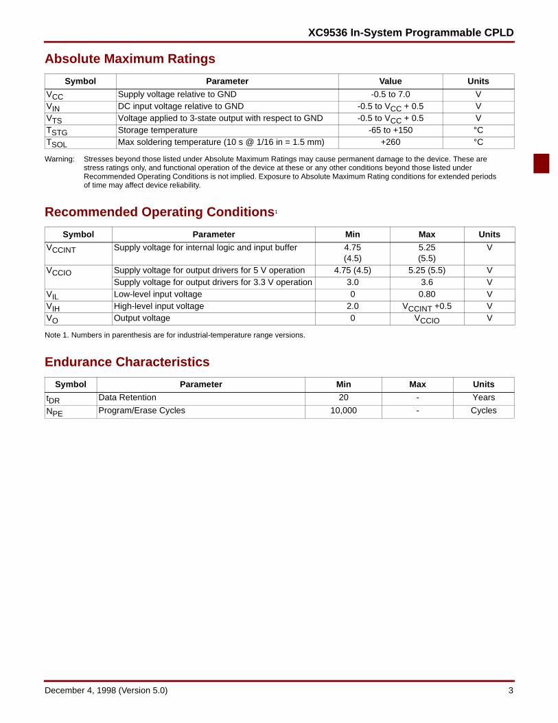
Absolute Maximum Ratings
Warning: Stresses beyond those listed under Absolute Maximum Ratings may cause permanent damage to the device. These are stress ratings only, and functional operation of the device at these or any other conditions beyond those listed under Recommended Operating Conditions is not implied. Exposure to Absolute Maximum Rating conditions for extended periods of time may affect device reliability.
Recommended Operating Conditions1
Note 1. Numbers in parenthesis are for industrial-temperature range versions.
Endurance Characteristics
Symbol Parameter Value Units
VCC Supply voltage relative to GND -0.5 to 7.0 VVIN DC input voltage relative to GND -0.5 to VCC + 0.5 VVTS Voltage applied to 3-state output with respect to GND -0.5 to VCC + 0.5 VTSTG Storage temperature -65 to +150 °CTSOL Max soldering temperature (10 s @ 1/16 in = 1.5 mm) +260 °C
Symbol Parameter Min Max Units
VCCINT Supply voltage for internal logic and input buffer 4.75(4.5)
5.25(5.5)
V
VCCIO Supply voltage for output drivers for 5 V operation 4.75 (4.5) 5.25 (5.5) VSupply voltage for output drivers for 3.3 V operation 3.0 3.6 V
VIL Low-level input voltage 0 0.80 VVIH High-level input voltage 2.0 VCCINT +0.5 VVO Output voltage 0 VCCIO V
Symbol Parameter Min Max Units
tDR Data Retention 20 - Years
NPE Program/Erase Cycles 10,000 - Cycles
December 4, 1998 (Version 5.0) 3
XC9536 In-System Programmable CPLD
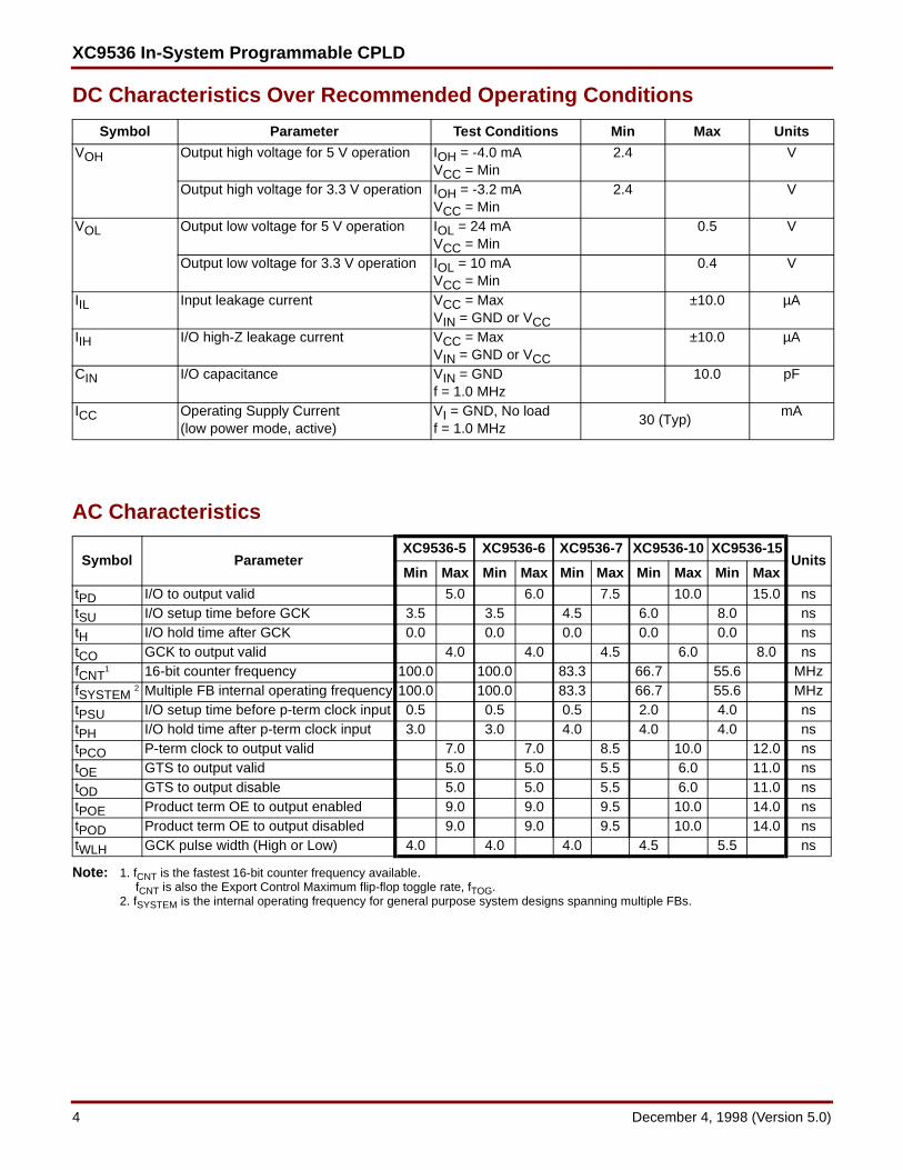
DC Characteristics Over Recommended Operating Conditions
AC Characteristics
Note: 1. fCNT is the fastest 16-bit counter frequency available. fCNT is also the Export Control Maximum flip-flop toggle rate, fTOG.
2. fSYSTEM is the internal operating frequency for general purpose system designs spanning multiple FBs.
Symbol Parameter Test Conditions Min Max Units
VOH Output high voltage for 5 V operation IOH = -4.0 mA VCC = Min
2.4 V
Output high voltage for 3.3 V operation IOH = -3.2 mA VCC = Min
2.4 V
VOL Output low voltage for 5 V operation IOL = 24 mA VCC = Min
0.5 V
Output low voltage for 3.3 V operation IOL = 10 mA VCC = Min
0.4 V
IIL Input leakage current VCC = MaxVIN = GND or VCC
±10.0 µA
IIH I/O high-Z leakage current VCC = MaxVIN = GND or VCC
±10.0 µA
CIN I/O capacitance VIN = GNDf = 1.0 MHz
10.0 pF
ICC Operating Supply Current (low power mode, active)
VI = GND, No loadf = 1.0 MHz
30 (Typ)mA
Symbol ParameterXC9536-5 XC9536-6 XC9536-7 XC9536-10 XC9536-15
UnitsMin Max Min Max Min Max Min Max Min Max
tPD I/O to output valid 5.0 6.0 7.5 10.0 15.0 nstSU I/O setup time before GCK 3.5 3.5 4.5 6.0 8.0 nstH I/O hold time after GCK 0.0 0.0 0.0 0.0 0.0 nstCO GCK to output valid 4.0 4.0 4.5 6.0 8.0 nsfCNT
1 16-bit counter frequency 100.0 100.0 83.3 66.7 55.6 MHzfSYSTEM
2 Multiple FB internal operating frequency 100.0 100.0 83.3 66.7 55.6 MHztPSU I/O setup time before p-term clock input 0.5 0.5 0.5 2.0 4.0 nstPH I/O hold time after p-term clock input 3.0 3.0 4.0 4.0 4.0 nstPCO P-term clock to output valid 7.0 7.0 8.5 10.0 12.0 nstOE GTS to output valid 5.0 5.0 5.5 6.0 11.0 nstOD GTS to output disable 5.0 5.0 5.5 6.0 11.0 nstPOE Product term OE to output enabled 9.0 9.0 9.5 10.0 14.0 nstPOD Product term OE to output disabled 9.0 9.0 9.5 10.0 14.0 nstWLH GCK pulse width (High or Low) 4.0 4.0 4.0 4.5 5.5 ns
4 December 4, 1998 (Version 5.0)

XC9536 In-System Programmable CPLD
Internal Timing Parameters
Note: 3. tPTA is multiplied by the span of the function as defined in the family data sheet.
Symbol ParameterXC9536-5 XC9536-6 XC9536-7 XC9536-10 XC9536-15
UnitsMin Max Min Max Min Max Min Max Min Max
Buffer DelaystIN Input buffer delay 1.5 1.5 2.5 3.5 4.5 nstGCK GCK buffer delay 1.5 1.5 1.5 2.5 3.0 nstGSR GSR buffer delay 4.0 4.0 4.5 6.0 7.5 nstGTS GTS buffer delay 5.0 5.0 5.5 6.0 11.0 nstOUT Output buffer delay 2.0 2.0 2.5 3.0 4.5 nstEN Output buffer enable/disable delay 0.0 0.0 0.0 0.0 0.0 nsProduct Term Control DelaystPTCK Product term clock delay 3.0 3.0 3.0 3.0 2.5 nstPTSR Product term set/reset delay 1.0 1.0 2.0 2.5 3.0 nstPTTS Product term 3-state delay 5.5 5.5 4.5 3.5 5.0 nsInternal Register and Combinatorial delaystPDI Combinatorial logic propagation delay 0.5 1.5 0.5 1.0 3.0 nstSUI Register setup time 2.5 2.5 1.5 2.5 3.5 nstHI Register hold time 1.0 1.0 3.0 3.5 4.5 nstCOI Register clock to output valid time 0.5 0.5 0.5 0.5 0.5 nstAOI Register async. S/R to output delay 6.0 6.0 6.5 7.0 8.0 nstRAI Register async. S/R recovery before clock 5.0 5.0 7.5 10.0 10.0 nstLOGI Internal logic delay 1.0 1.0 2.0 2.5 3.0 nstLOGILP Internal low power logic delay 9.0 9.0 10.0 11.0 11.5 nsFeedback DelaystF FastCONNECT matrix feeback delay 6.0 6.0 8.0 9.5 11.0 nsTime AdderstPTA
3 Incremental Product Term Allocator delay 0.8 0.8 1.0 1.0 1.0 nstSLEW Slew-rate limited delay 3.5 3.5 4.0 4.5 5.0 ns
R1
VTEST
CLR2
Device Output
Output Type VTEST
5.0 V
3.3 V
R1
160 Ω260 Ω
R2
120 Ω360 Ω
CL
35 pF
35 pF
X5906
VCCIO
5.0 V
3.3 V
Figure 3: AC Load Circuit
December 4, 1998 (Version 5.0) 5

XC9536 In-System Programmable CPLD
XC9536 I/O Pins
XC9536 Global, JTAG and Power Pins
FunctionBlock Macrocell PC44 VQ44 CS48 BScan
Order Notes FunctionBlock Macrocell PC44 VQ44 CS48 BScan
Order Notes
1 1 2 40 D6 105 2 1 1 39 D7 511 2 3 41 C7 102 2 2 44 38 E5 481 3 5 43 B7 99 [1] 2 3 42 36 E6 45 [1]1 4 4 42 C6 96 2 4 43 37 E7 421 5 6 44 B6 93 [1] 2 5 40 34 F6 39 [1]1 6 8 2 A6 90 2 6 39 33 G7 36 [1]1 7 7 1 A7 87 [1] 2 7 38 32 G6 331 8 9 3 C5 84 2 8 37 31 F5 301 9 11 5 B5 81 2 9 36 30 G5 271 10 12 6 A4 78 2 10 35 29 F4 241 11 13 7 B4 75 2 11 34 28 G4 21
1 12 14 8 A3 72 2 12 33 27 E3 181 13 18 12 B2 69 2 13 29 23 F2 151 14 19 13 B1 66 2 14 28 22 G1 121 15 20 14 C2 63 2 15 27 21 F1 91 16 22 16 C3 60 2 16 26 20 E2 61 17 24 18 D2 57 2 17 25 19 E1 31 18 – – - 54 2 18 - - - 0
Note: [1] Global control pin Note: [1] Global control pin
Pin Type PC44 VQ44 CS48
I/O/GCK1 5 43 B7I/O/GCK2 6 44 B6I/O/GCK3 7 1 A7I/O/GTS1 42 36 E6I/O/GTS2 40 34 F6I/O/GSR 39 33 G7
TCK 17 11 A1TDI 15 9 B3TDO 30 24 G2TMS 16 10 A2
VCCINT 5 V 21,41 15,35 C1,F7VCCIO 3.3 V/5 V 32 26 G3
GND 23,10,31 17,4,25 A5, D1, F3No Connects — — C4, D3, D4, E4
6 December 4, 1998 (Version 5.0)

XC9536 In-System Programmable CPLD
Ordering Information
Component Availability
C = Commercial (0°C to +70°C), I = Industrial (–40°C to +85°C)
Revision Control
Speed Options
-15 15 ns pin-to-pin delay-10 10 ns pin-to-pin delay
-7 7.5 ns pin-to-pin delay-6 6 ns pin-to-pin delay-5 5 ns pin-to-pin delay
Packaging Options
PC44 44-Pin Plastic Leaded Chip Carrier (PLCC)VQ44 44-Pin Thin Quad Pack (VQFP)CS48 48-Pin Chip Scale Package (CSP)
Temperature Options
C = Commercial (0°C to +70°C)I = Industrial (–40°C to +85°C)
XC9536 -5 PC 44 C
Device Type
SpeedPackage Type
Number of Pins
Temperature Range
Pins 44 48
TypePlasticPLCC
PlasticVQFP
PlasticCSP
Code PC44 VQ44 CS48
XC9536
–15 C,I C,I -–10 C,I C,I C–7 C,I C,I C–6 C C -–5 C C C
Date Reason6/3/98 Revise datasheet to reflect new CSP package pinouts & ordering code.
11/2/98 Revise datasheet to reflect new AC characteristics and Internal Timing Parameters.12/04/98 Revise datasheet to remove PCI compliancy statement and remove tLF.
December 4, 1998 (Version 5.0) 7

PLCC socket
PLCC socket is used to mount CPLD device on the printed board. PLCC is the abbreviation of "Plastic Leaded Chip Carrier".
There are lead pins to connect a printed board with the bottom of the socket. Because it is 0.1 inches in the pin interval, it is possible to mount on the universalprinted board, too.
To know the direction of the socket, you see from the top and you make a diagonal corner the upper left. The center of the line in the topside is the 1st pin. Ithink that you can find the mark of the triangle which shows the 1st pin inside the socket which puts CPLD.
As for the size of the socket, 44 pins are about 23 mm x 23 mm and 84 pins are about 37 mm x 37mm.
The figure on the left shows a pin diagram of the bottom view for 44 pins.
It is necessary to be careful so as not to make a mistake because there are many numbersof the pins.
The figure below shows a pin diagram of the bottom view for 84 pins.

Method of removing a device
A thin screwdriver can be used to remove CPLD device from the PLCC socket. There are ditchesfor removing at the corner of PLCC socket. Put the tip of the screwdriver in the ditch, and makethe top lift a device and remove it. Do alternately with the side of the opposite angle and lift slowly.Because there is possibility to give the damage to the device when handling violently, remove itcarefully.