Germanium as a material for Stimulated Brillouin ... as a... · Germanium as a material for...
12
Germanium as a material for Stimulated Brillouin Scattering in the mid-infrared C. Wolff, 1,2∗ R. Soref 3 , C.G. Poulton 1,2 B.J. Eggleton 1,4 , 1 Centre for Ultrahigh Bandwidth Devices for Optical Systems (CUDOS), Australia; 2 School of Mathematical Sciences, University of Technology Sydney, NSW 2007, Australia; 3 Department of Physics and the Engineering Program, The University of Massachusetts at Boston, Boston, MA 02125, USA; 4 Institute of Photonics and Optical Science (IPOS), School of Physics, University of Sydney, NSW 2006, Australia; ∗ [email protected] Abstract: We propose buried waveguides made of germanium or alloys of germanium and other group-IV elements as a fully CMOS-compatible plat- form for robust, high-gain stimulated Brillouin scattering (SBS) applications in the mid-infrared regime. To this end, we present numerical calculations for backward-SBS at 4 μ m in germanium waveguides that are buried in sil- icon nitride. Due to the strong photoelastic anisotropy of germanium, we investigate two different orientations of the germanium crystal with respect to the waveguide’s propagation direction and find considerable differences. The acoustic wave equation is solved including crystal anisotropy; acoustic losses are computed from the acoustic mode patterns and previously pub- lished material parameters. OCIS codes: (190.5890) ; (130.3060) ; (130.4310) . References and links 1. N.K. Hon, R.A. Soref, B. Jalali, “The third-order nonlinear optical coefficients of Si, Ge, and Si 1−x Ge x in the midwave and longwave infrared,” J. Appl. Phys. 110, 011301 (2011). 2. R.W. Boyd, Nonlinear optics (Academic Press, 3rd edition, 2003). 3. R.A. Soref, “Group IV photonics for the mid infrared,” Invited Plenary talk, SPIE Photonics West, OPTO con- ferences, paper 01-8629, Proceedings of the SPIE 8629 (2013). 4. R. Soref, “Silicon-based silicon-germanium-tin heterostructure photonics,” Phil. Trans. R. Soc. A 372, (2014). Doi: 10.1098/rsta.2013.0113. 5. R. Soref, “Mid-infrared photonics in silicon and germanium,” Nat. Photon. 4, 495 (2010) 6. B.J. Eggleton, C.G. Poulton, R. Pant, “Inducing and harnessing stimulated Brillouin scattering in photonic inte- grated circuits,” Adv. Opt. Photon. 5, 536-587 (2013). 7. P. T. Rakich, P. Davids, and Z. Wang, “Tailoring optical forces in waveguides through radiation pressure and electrostrictive forces,” Opt. Express 18, 14439 (2010) 8. J. Li, H. Lee, K.H. Vahala, “Low-noise Brillouin laser on a chip at 1064 nm,” Opt. Lett. 39, 287 (2014). 9. J. Li, H. Lee, K.H. Vahala, “Microwave synthesizer using an on-chip Brillouin oscillator,” Nature Comm., Doi: 10.1038/ncomms.3097 (28 June 2013, in press) 10. X. Yang, F. Cheng, R. Soref, “Single-mode GeSn mid-infrared waveguides on group-IV substrates,” paper JTh2A.57, Conference on Lasers and Electro-Optics (Applications and Technology), San Jose, CA (2014). 11. C. Wolff, M.J. Steel, B.J. Eggleton, C.G. Poulton, “Stimulated Brillouin Scattering in integrated photonic waveg- uides: forces, scattering mechanisms and coupled mode analysis,” arXiv:1407.3521 [physics.optics], (2014) 12. F. De Leonardis, B. Troia, V.M.N. Passaro, “Mid-IR Optical and Non Linear Properties of Germanium on Silicon Optical Waveguides,” J. Lightwave Technol. DOI:10.1109/JLT.2014.2339101, (2014, in press) 13. F. Sch¨ affler, “High-mobility Si and Ge structures,” Semiconductor Science and Technology 12, 1515 (1997) 14. J.J. Wortman, R.A. Evans “Young’s Modulus, Shear Modulus, and Poisson’s Ratio in Silicon and Germanium,” J. Appl. Phys. 36, 153 (1965) 15. D.K. Biegelsen, “Photoelastic Tensor of Silicon and the Volume Dependence of the Average Gap,” Phys. Rev. Lett. 32, 1196 (1974)
Transcript of Germanium as a material for Stimulated Brillouin ... as a... · Germanium as a material for...

Germanium as a material for Stimulated
Brillouin Scattering in the mid-infrared
C. Wolff,1,2∗ R. Soref3, C.G. Poulton1,2 B.J. Eggleton1,4,1 Centre for Ultrahigh Bandwidth Devices for Optical Systems (CUDOS), Australia;
2 School of Mathematical Sciences, University of Technology Sydney, NSW 2007, Australia;3 Department of Physics and the Engineering Program, The University of Massachusetts at
Boston, Boston, MA 02125, USA;4 Institute of Photonics and Optical Science (IPOS), School of Physics, University of Sydney,
NSW 2006, Australia;∗[email protected]
Abstract: We propose buried waveguides made of germanium or alloys of
germanium and other group-IV elements as a fully CMOS-compatible plat-
form for robust, high-gain stimulated Brillouin scattering (SBS) applications
in the mid-infrared regime. To this end, we present numerical calculations
for backward-SBS at 4 µm in germanium waveguides that are buried in sil-
icon nitride. Due to the strong photoelastic anisotropy of germanium, we
investigate two different orientations of the germanium crystal with respect
to the waveguide’s propagation direction and find considerable differences.
The acoustic wave equation is solved including crystal anisotropy; acoustic
losses are computed from the acoustic mode patterns and previously pub-
lished material parameters.OCIS codes: (190.5890) ; (130.3060) ; (130.4310) .
References and links
1. N.K. Hon, R.A. Soref, B. Jalali, “The third-order nonlinear optical coefficients of Si, Ge, and Si1−xGex in the
midwave and longwave infrared,” J. Appl. Phys. 110, 011301 (2011).
2. R.W. Boyd, Nonlinear optics (Academic Press, 3rd edition, 2003).
3. R.A. Soref, “Group IV photonics for the mid infrared,” Invited Plenary talk, SPIE Photonics West, OPTO con-
ferences, paper 01-8629, Proceedings of the SPIE 8629 (2013).
4. R. Soref, “Silicon-based silicon-germanium-tin heterostructure photonics,” Phil. Trans. R. Soc. A 372, (2014).
Doi: 10.1098/rsta.2013.0113.
5. R. Soref, “Mid-infrared photonics in silicon and germanium,” Nat. Photon. 4, 495 (2010)
6. B.J. Eggleton, C.G. Poulton, R. Pant, “Inducing and harnessing stimulated Brillouin scattering in photonic inte-
grated circuits,” Adv. Opt. Photon. 5, 536-587 (2013).
7. P. T. Rakich, P. Davids, and Z. Wang, “Tailoring optical forces in waveguides through radiation pressure and
electrostrictive forces,” Opt. Express 18, 14439 (2010)
8. J. Li, H. Lee, K.H. Vahala, “Low-noise Brillouin laser on a chip at 1064 nm,” Opt. Lett. 39, 287 (2014).
9. J. Li, H. Lee, K.H. Vahala, “Microwave synthesizer using an on-chip Brillouin oscillator,” Nature Comm., Doi:
10.1038/ncomms.3097 (28 June 2013, in press)
10. X. Yang, F. Cheng, R. Soref, “Single-mode GeSn mid-infrared waveguides on group-IV substrates,” paper
JTh2A.57, Conference on Lasers and Electro-Optics (Applications and Technology), San Jose, CA (2014).
11. C. Wolff, M.J. Steel, B.J. Eggleton, C.G. Poulton, “Stimulated Brillouin Scattering in integrated photonic waveg-
uides: forces, scattering mechanisms and coupled mode analysis,” arXiv:1407.3521 [physics.optics], (2014)
12. F. De Leonardis, B. Troia, V.M.N. Passaro, “Mid-IR Optical and Non Linear Properties of Germanium on Silicon
Optical Waveguides,” J. Lightwave Technol. DOI:10.1109/JLT.2014.2339101, (2014, in press)
13. F. Schaffler, “High-mobility Si and Ge structures,” Semiconductor Science and Technology 12, 1515 (1997)
14. J.J. Wortman, R.A. Evans “Young’s Modulus, Shear Modulus, and Poisson’s Ratio in Silicon and Germanium,”
J. Appl. Phys. 36, 153 (1965)
15. D.K. Biegelsen, “Photoelastic Tensor of Silicon and the Volume Dependence of the Average Gap,” Phys. Rev.
Lett. 32, 1196 (1974)

16. A. Feldman, R.M. Waxler, D. Horowitz, “Photoelastic constants of germanium,” J. Appl. Phys. 49, 2589 (1978)
17. B.G. Helme, P.J. King, “The Phonon Viscosity Tensor of Si, Ge, GaAs, and InSb,” phys. stat. sol. (a) 45, K33
(1978)
18. F. Schaffler, 149-188, in Properties of Advanced SemiconductorMaterials GaN, AlN, InN, BN, SiC, SiGe, M.E.
Levinshtein, S.L. Rumyantsev, M.S. Shur, ed. (John Wiley & Sons, Inc., New York, 2001)
19. W. Zhou, Z. Ma, S. Chuwongin, Y.C. Shuai, J.H. Seo, D. Zhao, H. Yang, W. Yang, “Semiconductor nanomem-
branes for integrated silicon photonics and flexible Photonics” (invited), Op. Quant. Electron. 44, 12-13 (2012)
20. W. Zhou, Z. Ma, W. Yang, S. Chuwongin, Y.C. Shuai, J.H. Seo, D. Zhao, H. Yang, R. Soref, “Semiconductor
nanomembranes for integrated and flexible photonics” (invited) Digest of Papers, Information Photonics 2011
Conference, Ottawa (18 May 2011).
21. E.P. Ippen, R.H. Stolen, “Stimulated Brillouin scattering in optical fibers, ” Appl. Phys. Lett. 21, 539–541 (1972).
22. K.S. Abedin, “Observation of strong stimulated Brillouin scattering in single-mode As2Se3 chalcogenide fiber,”
Opt. Express 13, 10266–10271 (2005).
23. R. Pant, C.G. Poulton, D.-Y. Choi, H. Mcfarlane, S. Hile, E. Li, L. Thevenaz, B. Luther-Davies, S.J. Madden,
B.J. Eggleton, “On-chip stimulated Brillouin scattering,” Opt. Express 19, 8285–8290 (2011).
1. Introduction
The third-order nonlinear optical (NLO) properties of group IV semiconductors [1] are receiv-
ing increased attention for practical applications. Early work on Raman gain and Raman lasing
is being supplanted by the rapidly emerging science and technology of Stimulated Brillouin
scattering (SBS) which is the strongest NLO process [2]. The elemental semiconductors Si
and Ge and more generally the crystal alloy SiGeSn are the prime group-IV SBS candidates.
These materials are the material focus of of “group IV photonics” which is a practical silicon-
based technology for high-volume photonic-circuit manufacture in a CMOS opto-electronic
foundry. Along with Ge, the “Ge-rich” materials SiGe and GeSn are the most important semi-
conductors for migrating the near-infrared (NIR, i.e. 1.31-1.55 µm) group IV photonics into the
mid-infrared (MIR) region [3–5], initially at wavelengths of 1.8 to 5.0 µm and eventually to-
wards 14 µm. The migration has begun and momentum in this research area is building rapidly.
Group IV photonics at MIR–as in the 1.3/1.6 µm telecommunications bands–has wide-ranging
sensing and communications applications [3–5] and is CMOS-compatible.
A recent review discussed techniques for exciting SBS in a chip-scale photonic integrated
circuit[6]. In the long run, chips and waveguide-integrated on-chip networks are attractive Bril-
louin platforms, especially because the necessary active waveguides can be spiraled in-plane
to supply long lengths if needed. Currently, many such on-chip experiments are based on soft-
glass waveguides with substantial SBS-gains of the order of 13dB/cm per Watt of pump power
at 1.55 µm. These glasses remain very suitable for experiments at larger wave lengths. However,
as for any other waveguide, their total device gain will be reduced because of the greater ef-
fective mode area at longer wave lengths and the resulting lower optical intensities for a given
pump power. As a CMOS-compatible alternative with much higher gains at 1.55 µm, much
attention has been recently devoted to suspended silicon waveguides with very small cross sec-
tions [7] deriving their extraordinarily high SBS gains from a combination of small modal area
and radiation pressure effects. Although this approach clearly could provide extremely efficient
MIR-SBS-devices, these waveguides typically have to be completely or nearly completely sus-
pended over long distances to ensure optical and acoustic mode confinement, resulting in me-
chanically fragile devices and difficult fabrication. These two options for SBS-devices are basi-
cally extensions of the current research being performed in the NIR. In contrast, Ge and Ge-rich
group-IV-semiconductors are genuine MIR-materials and deserve being studied for their appli-
cability in the context of SBS in the mid-infrared. These materials feature a very high index
of refraction at a low speed of sound as compared to e.g. Si, therefore need not be suspended
and (as we will show) can provide very competitive SBS-gain in an inherently rugged design.
In addition, these materials exhibit strong electrostriction and are fully compatible with estab-
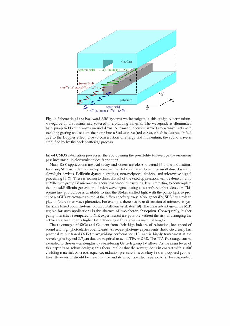
Fig. 1: Schematic of the backward-SBS systems we investigate in this study: A germanium-
waveguide on a substrate and covered in a cladding material. The waveguide is illuminated
by a pump field (blue wave) around 4 µm. A resonant acoustic wave (green wave) acts as a
traveling grating and scatters the pump into a Stokes wave (red wave), which is also red-shifted
due to the Doppler effect. Due to conservation of energy and momentum, the sound wave is
amplified by by the back-scattering process.
lished CMOS fabrication processes, thereby opening the possibility to leverage the enormous
past investment in electronic device fabrication.
Many SBS applications are real today and others are close-to-actual [6]. The motivations
for using SBS include the on-chip narrow-line Brillouin laser, low-noise oscillators, fast- and
slow-light devices, Brillouin dynamic gratings, non-reciprocal devices, and microwave signal
processing [6, 8]. There is reason to think that all of the cited applications can be done on-chip
at MIR with group IV micro-scale acoustic-and-optic structures. It is interesting to contemplate
the optical/Brillouin generation of microwave signals using a fast infrared photodetector. This
square-law photodiode is available to mix the Stokes-shifted light with the pump light to pro-
duce a 6GHz microwave source at the difference-frequency. More generally, SBS has a role to
play in future microwave photonics. For example, there has been discussion of microwave syn-
thesizers based upon photonic on-chip Brillouin oscillators [9]. The clear advantage of the MIR
regime for such applications is the absence of two-photon absorption. Consequently, higher
pump intensities (compared to NIR experiments) are possible without the risk of damaging the
active area, leading to a higher total device gain for a given waveguide length.
The advantages of SiGe and Ge stem from their high indexes of refraction, low speed of
sound and high photoelastic coefficients. As recent photonic experiments show, Ge clearly has
practical mid-infrared (MIR) waveguiding performance [10] and is highly transparent at the
wavelengths beyond 3.7 µm that are required to avoid TPA in SBS. The TPA-free range can be
extended to shorter wavelengths by considering Ge-rich group-IV alloys. As the main focus of
this paper is on robust designs; this focus implies that the waveguide is in contact with a stiff
cladding material. As a consequence, radiation pressure is secondary in our proposed geome-
tries. However, it should be clear that Ge and its alloys are also superior to Si for suspended,

radiation-pressure-dominated devices in the MIR because of their higher refractive indices.
The photoelastic properties of Ge are highly anisotropic, therefore all mechanical equations are
solved numerically in their most general anisotropic form. The acoustic quality factors of the
waveguides are calculated from measured values of the dynamic viscosity tensor. A discovery
made in this paper is that the [110] orientation of a crystalline Ge photonic channel waveguides
provides significantly better acousto-optic coupling than does the [100]-oriented channel. The
consequences of [110] are examined, and the Ge channel is optimized in its Si3N4 cladding, a
favorable acoustic material that is transparent out to ∼ 8 µm. Also optimized are the geomet-
ric size-and-shape of the microwave acoustic waveguide and the interacting light-confinement
shape. As a result of this maximizing at λ = 4 µm, we predict in this waveguide large backward-
travelling SBS gains that are in the range of 33 to 46dB/cm per Watt of pump power. This is to
be compared to 13dB/cm per Watt for a chalcogenide rib waveguide at 1.55 µm. Waveguides
of Ge-rich [110] SiGeSn cover the 3 to 8 µm range [10] where the cladding is transparent and
where TPA is eliminated. SBS optical power gain is analyzed in this paper and Ge photonic
waveguides are specially engineered here for this acoustic/optic application.
2. SBS-equations of motion
We base this work on our previous publication on theoretical aspects of SBS in integrated pho-
tonic waveguides [11], using the same notation and expressions. The optical fields are expressed
as a superposition of two eigenmodes. For the electric field, this results in the ansatz
E =e(1)(r, t) a(1)(z, t)+ e(2)(r, t) a(2)(z, t) + c.c. , (1)
=e(1)a(1) exp(iβ (1)z− iω(1)t)+ e(2)a(2) exp(iβ (1)z− iω(1)t) + c.c. , (2)
where c.c. denotes the complex conjugate terms and the envelopes a(i)(z, t) are slowly varying
functions of the longitudinal coordinate and time. The mode patterns e(i)(x,y) are functions of
the transverse coordinates and solutions to the optical wave equation with wave vector zβ (i)
and angular frequency ω(i). The power P(i) = |a(i)|2P(i) transmitted in one optical channel i
is determined by the modal power P(i) and the respective envelope function. As we focus on
backward SBS, we can approximate the Stokes mode (superscript 1) as the time-reversed pump
mode (superscript 2):
e(1) ≈ [e(2)]∗; β (1) ≈−β (2); P(1) ≈−P
(2). (3)
The acoustic excitation is expressed as a modulated acoustic eigenmode with envelope func-
tion b(z, t). Thus, the expansion for the mechanic displacement field reads
U(r, t) = u(r, t)b(z, t)+ c.c. = u(x,y)b(z, t)exp(iqz− iΩt)+ c.c.; (4)
with ρΩ2ui +∑jkl
(∇⊥+ iqz) j ci jkl (∇⊥+ iqz)k ul = 0. (5)
Here, ρ and c are the materials’ densities and stiffness tensors, respectively. The acoustic and
the two optical modes must be phase-matched to the beat of the optical modes:
q = β (2)−β (1) ≈ 2β (2), Ω = ω(2)−ω(1). (6)
In analogy to the optical modes, we introduce the symbol Pb for the power of the acoustic
mode with unit envelope b = 1.
We assume steady state and the long waveguide approximation for the envelope func-
tions [11]. Within this approximations, the evolution of the optical powers along the waveguide
can be expressed in terms of the transmitted powers:
∂zP(1) =ΓP(1)P(2), ∂zP
(2) =−ΓP(1)P(2), (7)
where
Γ =2ωΩ|Q|2
P(1)P(2)Pbα(8)
is the SBS power gain on resonance. The acoustic decay parameter α is determined by the
acoustic mode pattern and the dynamic viscosity η of the waveguide materials:
α =Ω2
Pb
∫d2r ∑
jkl
u∗i ∂ jηi jkl∂kul
, (9)
where the integral is carried out over the whole transversal plane. The final required quantity
in Eqn. (8) is the acousto-optic perturbation integral Q, i.e. the overlap between the optical
eigenmodes and the field perturbations caused by the acoustic excitation. Using Eqn. (3), this
is [11]
Q =∫
C
dr (u∗ · n)[(εa − εb)ε0(n× e(2))(n× e(2))− (ε−1
b − ε−1a )ε−1
0 (n ·d(2))(n ·d(2))]
+ ε0
∫d2r ∑
i jkl
ei(2)e j
(2)ε2r pi jkl∂ku∗l + iΩµ0ε0
∫d2r (εr −1)u∗ · (e(2)×h(2)). (10)
where d(2) and h(2) are the electric induction field and the magnetic field distributions of the op-
tical pump eigenmode. The first integral is a line integral to be carried out along all boundaries
with normal vector n between different materials with relative permittivities εa and εb, respec-
tively. The other two integrals extend over the whole transversal plane, where the photoelastic
tensor p(x,y) and the relative permittivity εr(x,y) are functions of the transverse coordinates.
3. Acousto-optical design guidelines
SBS is the resonant interaction between a sound wave and two light waves in matter. For this
to be efficient all three modes must be tightly confined in the same volume with good mode
overlap. Here, we focus on index-guided waveguides, where the guided modes are confined by
total internal reflection in the material with the lowest phase velocity. For the optical modes this
is the material with the highest relative permittivity εr. For acoustic waves, the speed of sound
vph =√
cproj/ρ is determined by the appropriately projected elasticity modulus cproj (e.g. the
shear modulus for bulk shear waves) and the mass density ρ . It is lowest for soft and dense
materials. The ideal material for an SBS-active waveguide is therefore soft, dense and has a
high refractive index.
Good acoustic confinement and consequently sharp SBS-resonances can be obtained if the
phase velocity of the SBS-active acoustic mode is smaller than the phase velocity of any other
acoustic mode it can couple to. This means that a waveguide must either be suspended in air or
surrounded by a stiff cladding material. The former is a very elegant solution to the problem of
acoustic leakage and has the further advantage that radiation pressure (i.e. the discontinuity of
Maxwell’s stress tensor across material boundaries) can significantly enhance the acousto-optic
interaction [7]. However, such suspended structures are not easy to fabricate over appreciable
length and tend to be rather fragile. The latter design with a high-index waveguide embedded
in a stiff cladding has clear practical advantages and shall be the focus of this paper. However,
the problem of acoustic confinement imposes quite strict restrictions on the choice of material
combinations. The reason for this is the fact that longitudinal modes—at least for backward-
SBS the relevant mode is of this type—travel at speeds up to 50% faster than shear modes,
depending on the material’s effective Poisson ratio. If the waveguide can acoustically couple

to the boundary between the cladding material and free space, the maximum speed of confined
acoustic waveguide modes is determined by the substrate’s Rayleigh waves, which typically
travel at around 90% the speed of a bulk shear wave. Thus, the cladding material must be
considerably (roughly by a factor of two) stiffer than the waveguide material in order to allow
for backward-SBS. Such a minimum contrast does not exist for the permittivity – even a small
index contrast results in a guided mode. Finally, high SBS-gains typically require good spatial
overlap of the optical and the acoustic modes.
A Ge-waveguide on a high-index substrate such as Si has been recently studied especially in
the context of Kerr-nonlinearities [12] and in fact could be a potential candidate for an SBS-
active system. Some uncertainty arises because the shallow acoustic confinement of the Ge-Si
material pair could be broken by internal strains due to lattice mismatch. A second disadvantage
of this geometry is the poor mode overlap. This is due to the fact the optical mode tends to be
concentrated in high-index regions, hence it will be strongly pulled towards the substrate. The
acoustic mode, on the other hand, will be effectively clamped wherever the waveguide touches
the necessarily stiff substrate material. Conversely, it will be strongly attracted by any interface
between the waveguide material and free air (depending on th waveguide polarization, this can
lead to significant radiation pressure effects). As a consequence, to optical and acoustic modes
are separated from each other in a strongly asymmetric arrangement such as a Ge-waveguide
on a Si-substrate. At least this problem can be completely resolved by burying the waveguide
in the substrate material; in a buried waveguide both optical and acoustic modes are confined
in the waveguide’s center for symmetry reasons. As an additional practical advantage, a buried
waveguide is well isolated from environmental influences such as optically lossy contaminants.
For these reasons, we will focus on buried waveguides in the remainder of this paper.
4. MIR waveguide materials
The theoretical considerations outlined above are generic and in no way specific to the MIR
spectral range. What distinguishes this range from the NIR telecom range around 1550nm is
the choice of materials with low dielectric loss [5]. For example, silica, despite being one of
the main materials for CMOS-compatible integrated photonics in the NIR, becomes fairly lossy
around 3.5µm and is therefore not ideal as a cladding of MIR waveguides. On the other hand,
germanium and its alloys start to have excellent optical properties beyond 2µm and are natural
candidates for high-index waveguides.
Germanium has several advantages over silicon as a material for SBS-active waveguides.
Firstly, its relative electric permittivity is greater than that of silicon by about 30%. This results
in a stronger acousto-optic coupling in general, because all optical force terms involve at least
one factor of εr. Secondly, germanium features photoelastic tensor components with greater
absolute values compared to silicon; the values for pxxxx and pxyxy e.g. are greater by about 50%
(see Tab. 1). The main difference, however, is the much stronger anisotropy of germanium: In
an isotropic material, the tensor component pxxyy is directly related to the former two: pxxyy =pxxxx − 2pxyxy. For silicon and germanium, this would result in values of pxxyy of 0.008 and
−0.007, respectively (see Tab. 1). While this is very close to the actual value in the case of
silicon, it is off by nearly a factor of 20 for germanium. The corresponding Zener factors are
1.09 (silicon) and 0.16 (germanium), once again highlighting the strong photoelastic anisotropy
of germanium. This can be attributed to the fact that the dominant minima of the conduction
band in germanium are located at the four L-points within the first Brillouin zone, whereas
the relevant band minima for silicon are near the three X-points [13]. As a third advantage,
germanium has a lower speed of sound than silicon due to its higher mass density and smaller
stiffness constants. It thus comes rather close to the ideal waveguide material, which ensures
both optical and acoustic confinement while having strong opto-mechanical coupling.

Fig. 2: Sketches of a waveguide (gray) composed of a semiconductor with cubic symmetry on
an isotropic substrate (cyan) for the two crystal orientations that we consider in this paper. We
generally chose the Cartesian coordinate system according to the system’s geometry, i.e. along
the substrate normal (we chose this to be the y-axis) and the waveguide’s propagation direction
(we chose this to be the z-axis). We focus on two cases for two orientations of the material
tensors’ principal axes: a) shows a waveguide with the all cubic axes aligned with the Cartesian
frame of reference. We refer to this (slightly inaccurately) as the waveguide being composed
of a [100]-semiconductor; b) shows a waveguide where the cubic crystal is rotated by 45 with
respect to the Cartesian frame of reference around the surface normal (y-axis). We refer to this
as a waveguide composed of a [110]-semiconductor.
In previous works, the waveguide material was usually modelled as an isotropic material
when computing the acoustic modes. This is strictly correct for amorphous materials such as
soft glasses or silica and is clearly the best available option in the case of crystalline materials
if the orientation of the waveguide relative to the crystal axes is unknown. However, the strong
photoelastic anisotropy alone makes such an approach questionable for germanium as any rea-
sonably accurate calculation of the acousto-optic interaction requires knowledge of the crystal
orientation. The waveguide orientation on the wafer therefore becomes an essential design pa-
rameter. As a consequence, there is no reason not to solve the acoustic wave equation Eqn. (5)
including the full crystal anisotropy. In this paper, we restrict ourselves to two cases (see Fig. 2);
one where the waveguide axis is along the [100]-direction of the semiconductor and one where
it is aligned with the [110]-direction. In both cases, we assume the vertical direction to be [001].
In the former case, the coordinate system in which the acoustic wave equation Eqn. (5) is for-
mulated coincides with the crystal’s main axis system. In this coordinate frame, the material
tensors of a cubic material have the familiar symmetries such as cxxxx = cyyyy = czzzz for the
stiffness tensor. In the latter case, however, only one crystal axis is aligned with the coordinate
frame. For a waveguide aligned along the [110]-direction, the material parameters have tetrago-
nal symmetry, because the face-centered cubic lattice is identical to a body-centered tetragonal
lattice rotated by 45 around one principal axis. Finally, the acoustic losses of a waveguide
structure depend on the material properties, the geometry (including crystal orientation) and
the acoustic mode pattern. Experimental values for the dynamic viscosity η of several semi-
conductors at the target frequency range are available in the literature [14–17] and allow the
prediction of acoustic quality factors via Eqn. (9). The material properties of silicon and ger-
manium within the respective coordinate frames are listed in Tab. 1.
However, pure germanium also has one major disadvantage in that its band gap is only
0.65eV, corresponding to photons with a vacuum wavelength of 1825nm. As a consequence,
optical modes are subject to two-photon absorption down to a vacuum wavelength of 3650nm.
This includes the (possibly experimentally desirable) MIR line of helium-neon lasers at
3390nm. One way to overcome this problem is to use a silicon-germanium alloy SixGe1−x.
For sufficiently low silicon contents x, these materials have properties that are similar to pure
germanium, especially with regard to its anisotropic photoelastic tensor. We may expect this
to remain a good approximation as long as the band structure of the alloy has its conduction

Structure of fourth rank material tensors (Voigt notation):
Si[100], Ge[100] and Si3N4 Si[110] and Ge[110]
a11 a12 a12 0 0 0
a12 a11 a12 0 0 0
a12 a12 a11 0 0 0
0 0 0 a44 0 0
0 0 0 0 a44 0
0 0 0 0 0 a44
a11 a12 a13 0 0 0
a12 a22 a12 0 0 0
a13 a12 a11 0 0 0
0 0 0 a44 0 0
0 0 0 0 a55 0
0 0 0 0 0 a44
Values of material parameters:
quantity unit Ge [100] Ge [110] Si [100] Si [110] Si3N4
εr – 16.2 16.2 11.7 11.7 3.84
ρ kg/m3 5323 5323 2329 2329 3290
c11 GPa 129 156 166 194 387
c22 GPa 129 166
c12 GPa 47.9 47.9 63.9 63.9 143
c13 GPa 21.5 35.2c44 GPa 67.0 67.0 79.6 79.6 122
c55 GPa 40.6 50.9p11 – −0.151 −0.212 −0.094 −0.090 –
p22 – −0.151 −0.094
p12 – −0.128 −0.128 0.017 0.017 –
p13 – −0.068 0.013
p44 – −0.072 −0.072 −0.051 −0.051 –
p55 – −0.012 −0.056
η11 mPa · s 9.06 9.52 5.90 6.15 –
η22 mPa · s 9.06 5.90
η12 mPa · s 8.57 8.57 5.16 5.16 –
η13 mPa · s 8.11 4.91
η44 mPa · s 0.71 0.71 0.62 0.62 –
η55 mPa · s 0.25 0.37
Table 1: This table contains the material parameters for the structures that we investigate in this
paper. For the [100]-orientation of the cubic materials and for silicon nitride, the values for the
stiffness [14] tensor c, the photoelastic [15, 16] tensor p, and the viscosity [17] tensor η were
taken from their respective references. The values for the [110]-orientation were obtained from
those by applying a π/4-rotation around the y-axis. As a consequence, the fourth rank tensors
in the rotated coordinate frame lose the properties that are typical for a cubic material and
appear to describe a material with tetragonal symmetry. Neither any properties of an isotropic
material nor the scalar and second rank tensor properties of a cubic material are affected by the
rotation. The parameters in this table are valid for light of vacuum wavelength around 3500nm
and for acoustic frequencies in the GHz-range. We were unable to retrieve reliable data for
some material parameters of amorphous Si3N4 in the target frequency range.
band minima at the L-points, which is the case for x < 0.15 [13]. This is sufficient to increase
the electronic band gap to more than 0.8eV, extending the spectral region that is free of two-
photon absorption beyond 3 µm. Not all material properties of these germanium-rich alloys

are known. The relative permittivity and the basic mechanical properties (density and stiffness)
have been published [18]. For x = 0.1, they differ from the values for pure germanium by less
than 5%. The photoelastic properties and the viscosity, however, are less well known. For the
viscosity, we suggest the values for pure germanium, but for the photoelastic properties a linear
interpolation between pure silicon and pure germanium should provide a conservative estimate.
As a CMOS-compatible substrate and cladding material with low loss over a wide spectral
range we focus on silicon nitride Si3N4 [5]. This material is ideal as a cladding for SBS-active
waveguides because it combines a fairly low relative electric permittivity of 3.84 with a very
high speed of sound. A germanium waveguide completely clad in Si3N4 has both excellent
optical and acoustic confinement. As a consequence, both optical and acoustic modes can be
tightly guided in a small waveguide cross section, resulting in high optical intensities, excellent
acousto-optic mode overlap and consequently high SBS-gain.
We assume the Si3N4-phase to be amorphous. Thus, the material tensors have the symmetries
of an isotropic material (see Tab. 1). Unfortunately, we were unable to find reliable numbers for
the photoelastic properties over the desired wavelength range. However, in its envisioned role
as a substrate of cladding material for a germanium waveguide, it can be expected that Si3N4
will not provide significant photoelastic coupling, because of the high permittivity contrast of
a factor of 4 (which enters the photoelastic effect quadratically) and the fact that the acoustic
wave will be mainly confined inside the germanium. Furthermore, we could not find data for
the dynamic viscosity of amorphous Si3N4 in the target frequency range. This could be more
of a problem, because the the relative importance of friction in the substrate will only depend
on the acoustic confinement. It seems advisable to check the sensitivity of the loss of a given
acoustic mode to changes in the substrate viscosity, e.g. by using the viscosity of the waveguide
material as a plausible estimate.
There are several practical possibilities for fabricating Ge channel waveguides, and in each
case the substrate is a silicon wafer-or-chip upon which a thick film of Si3N4 has been deposited.
The nanomembrane (NM) approach [19, 20] is to lift off a ∼ 0.5 µm NM of [110]-oriented
crystal Ge from a sacrificial Ge wafer and to transfer that NM to the substrate where it is
bonded to Si3N4/Si via atomic-like bonding. After that, the NM is etched into the channel
network. Subsequently, thick Si3N4 is deposited upon those channels. A second method is to
use a [110]-oriented Sisubstrate in which a tiny window is etched in the Si3N4 down to the
Si substrate. After that, epitaxial lateral overgrowth of aligned crystal Ge would proceed upon
the Si3N4 of the substrate, this layer growth being seeded by Si through the small window.
Processing of the Ge would be done after these steps.
5. Proposed SBS-active Ge-waveguides
In this section, we demonstrate the potential of integrated germanium waveguides for SBS-
applications in the MIR range. To this end, we show power gain figures for backward-SBS
of rectangular germanium-waveguides buried in silicon nitride assuming light with a vacuum
wavelength of 4 µm throughout.
5.1. Waveguide in [100]-direction
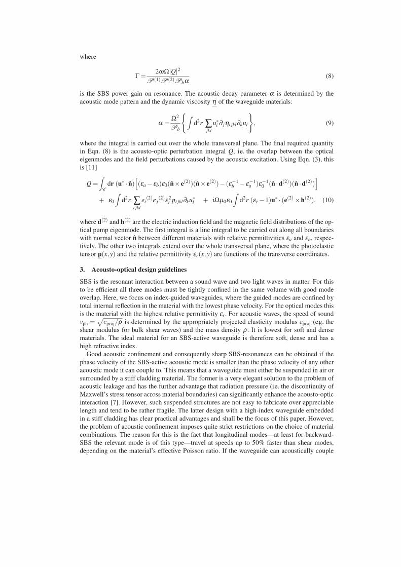
First, we study a Ge-waveguide aligned in the [100]-direction, using the values from the first
and the last column of Tab. 1. We find a maximum of Γ = 488W−1m−1 in the backward power
gain for a waveguide geometry of 1200× 550nm2 (see Fig. 3). The fact that the optimum is
close to a waveguide cross section with an aspect ratio of 2 can be traced back to the cubic
symmetry of the waveguide material: For symmetry reasons the acoustic mode must be even
under both reflection symmetries. For an acoustic mode with strong transversal components that
are nearly clamped at the interface to the cladding material, this suggests an acoustic mode with

0
100
200
300
400
500
pow
er g
ain
[W-1
m-1
]
5.5
6
6.5
7
7.5
Sto
kes
shift
[GH
z]
1 1.1 1.2 1.3 1.4waveguide width [µm]
0
100
200
300
400
deca
y le
ngth
[µm
]
1
2
point 1: width=1200nm
optical mode acoustic mode
point 2: width=1200nm
optical mode acoustic mode
air
+1 [a.u.]
-1 [a.u.]
0
Fig. 3: Results for backward-SBS of light with a vacuum wavelength of 4 microns in a germa-
nium waveguide in [100]-orientation buried in Si3N4. In the top right corner, we show a sketch
of the structure. The top plot to the left depicts the total power gain according to Eqn. (8) for
the lowest three symmetry-allowed acoustic modes as a function of the waveguide width while
the waveguide height is fixed at 550nm. The other two plots show the corresponding acoustic
frequencies and the acoustic decay lengths α−1, i.e. the inverse decay parameters according to
Eqn. (9), neglecting mechanical loss inside the cladding. Below the system sketch, we show the
optical and acoustic modes for points highlighted in the gain plot, i.e. for a waveguide width of
1200nm. The colorscale (in arbitrary units) is the z-component of the time-averaged Poynting
vector and the longitudinal component uz of the mechanical displacement field for the optical
and acoustic mode plots, respectively. The arrows indicate the in-plane electric field distribu-
tion and the in-plane components of the displacement field, the acoustic mode plots also contain
iso-contours of the in-plane acoustic displacement field norm√
|ux|2 + |uy|2 (thin blue lines).
The line colors in the plots and the frames around the mode plots match for identical acoustic
modes.
one maximum in the direction perpendicular to the main displacement direction and with one
maximum and one minimum along the main displacement direction. These two displacement
extrema are located in a region where the optical modal intensity rapidly changes, leading
to good photoelastic overlap. The central longitudinal displacement maximum is π/2rad out
of phase with the transversal components and has good photoelastic overlap with the central
maximum of the optical intensity. Both the acoustic and the optical mode (effective index 3.05)
are well confined. The data shown in Fig. 3 were calculated neglecting the photoelastic effect
and acoustic loss in the Si3N4-cladding. We checked the latter by repeating the calculation
for the 1200× 550nm2 geometry using a very roughly estimated viscosity for Si3N4: η11 =

0
200
400
600
800
1000
pow
er g
ain
[W-1
m-1
]
5.5
6
6.5
7
7.5
Sto
kes
shift
[GH
z]
0.7 0.8 0.9 1 1.1waveguide width [µm]
0
100
200
300
400
deca
y le
ngth
[µm
]
12
point 1: width=820nm
optical mode acoustic mode
point 2: width=1020nm
optical mode acoustic mode
air
+1 [a.u.]
-1 [a.u.]
0
Fig. 4: Results for backward-SBS of light with a vacuum wavelength of 4 microns in a germa-
nium waveguide in [110]-orientation buried in Si3N4. See the caption of Fig. 3 and the main
text for details.
9mPa ·s, η12 = 7.5mPa ·s, η44 =(η11−η12)/2. With this, the maximum power gain drops from
Γ = 488W−1m−1 to Γ = 479W−1m−1, which is small enough to be neglected. Our calculations
include radiation pressure at the interface between the germanium waveguide and the cladding,
but its contribution to the gain is small because the acoustic mode is nearly clamped at this
interface. The effective magnetic coupling term is extremely small and can be neglected. We
also note that the acoustic decay length α−1 strongly depends on the acoustic mode pattern and
the waveguide geometry as can be seen in Fig. 3. For the most strongly SBS-active mode, the
day length is around 300 µm, which corresponds to an acoustic Q-factor of just below 3000 for
the acoustic wave-vectors and frequencies in this example.
5.2. Waveguide in [110]-direction
As a second example, we study a similar Ge-waveguide, but this time aligned in the [110]-direction. In the previous section, the reason for the high aspect ratio is related to the cubic
symmetry of the material tensors of the waveguide material. So, we may expect this situation
to change when the crystal is rotated by 45. Indeed, we find the strongest interaction result-
ing in a backward power gain of Γ = 1056W−1m−1 for a nearly square-shaped waveguide
with a width of 820nm and a height of 700nm (see Fig. 4). The corresponding acoustic mode
resembles a compressed version of the optimal mode in the previous section. It differs very
significantly from the monopolar mode with radial symmetry in the transversal displacement
components, which would be expected for a nearly square waveguide composed of a material
with cubic stiffness tensor. Due to the higher mode confinement and better photoelastic overlap,

this setup results in a significantly higher backward gain compared to the best structure with
[100]-orientation. Perhaps the most striking feature in Fig. 4 is the presence of an anti-crossing
in the acoustic band structure around a waveguide width of 880nm with a steep dip in the ob-
tainable SBS-gain close to the optimal geometry. The acoustic loss figures in Fig. 4 do not
differ significantly from those shown in Fig. 3. However, this example using [110]-germanium
appears to be much more prone to acoustic loss in the cladding material: Again assuming the
previously mentioned very rough estimates for the dynamic viscosity of Si3N4, we find that
the backward gain is reduced from Γ = 1056W−1m−1 to 877W−1m−1 for the 820× 700nm2-
geometry (denoted position 1 in Fig. 4) and from Γ = 757W−1m−1 to Γ = 665W−1m−1 for the
1020×700nm2-geometry (denoted position 2).
6. Discussion
In the previous section, we presented two examples for SBS-active Ge-waveguides at λ = 4µm.
The predicted power gains for backward SBS ranged from roughly 500W−1m−1 for a waveg-
uide along the [100]-axis to roughly 1000W−1m−1 for the [110]-direction with Stokes shifts
around 6.5GHz. From the acoustic decay length and the acoustic wave vector we predict acous-
tic quality factors of the order of 2000 to 3000, which corresponds to a resonance linewidth
around 2-3MHz. In our examples, the waveguide was buried in Si3N4, which increases the
acousto-opto mode overlap, provides excellent acoustic confinement and isolates the waveg-
uide from exterior influences. Furthermore, the silicon nitride nearly clamps the acoustic mode
at the waveguide boundary with two main consequences. Firstly, the acoustic frequency is in-
creased. Secondly, the boundary contribution to the acousto-optic coupling integral (depending
one one’s viewpoint this is the radiation pressure or light scattering due to the acoustic boundary
displacement) is suppressed compared to a suspended waveguide. The presented waveguides
rely nearly entirely on the photoelastic effect of germanium.
Other SBS-systems that are used for SBS-applications and mainly exploit the photoelastic
effect are silica fibres [21], chalcogenide fibres [22] and chalcogenide rib waveguides for on-
chip photonic applications [23]. Among these, the latter already serve the intended purpose of
our proposed germanium waveguides. Their backward-SBS power gain was predicted to be
around Γ = 300W−1m−1 and such gains are commonly achieved [23] in NIR experiments with
resonance line widths around 30MHz at Stokes shifts around 7GHz. One conceptual disadvan-
tage of chalcogenide in integrated photonics, however, is its incompatibility with established
CMOS-processes. In contrast, the Si3N4-clad germanium waveguide is CMOS-compatible and
offers superior SBS-gain with an at least comparable resonance quality in the MIR regime.
Acknowledgments
This work was supported by the Australian Research Council (ARC) through its Discovery
grant (DP130100832), Center of Excellence (CUDOS, CE110001018) and Laureate Fellow-
ship (Prof. Eggleton, FL120100029) programs. R.S. is supported by the Air Force Office of
Scientific Research on grant FA9550-14-1-0196 (Gernot Pomrenke, Program Manager) and by
the UK EPSRC project MIGRATION.