GEORG-AUGUST-UNIVERSITAT¨ GOTTINGEN¨ II.PhysikalischesInstitut · Angenommen am: 31. Mai 2011 ......
87
GEORG-AUGUST-UNIVERSIT ¨ AT G ¨ OTTINGEN II. Physikalisches Institut Dynamic Efficiency Measurements for Irradiated ATLAS Pixel Single Chip Modules von Mike Pfaff The ATLAS pixel detector is the innermost subdetector of the ATLAS experiment. Due to this, the pixel detector has to be particularly radiation hard. In this diploma thesis effects on the sensor and the electronics which are caused by irradiation are examined. It is shown how the behaviour changes between an unirradiated sample and a irradiated sample, which was treated with the same radiation dose that is expected at the end of the lifetime of ATLAS. For this study a laser system, which is used for dynamic efficiency measurements was constructed. Furthermore, the behaviour of the noise during the detection of a particle was evaluated studied. Post address: Friedrich-Hund-Platz 1 37077 G¨ ottingen Germany II.Physik-UniG¨o-Dipl-2011/05 II. Physikalisches Institut Georg-August-Universit¨ at G¨ ottingen May 2011
Transcript of GEORG-AUGUST-UNIVERSITAT¨ GOTTINGEN¨ II.PhysikalischesInstitut · Angenommen am: 31. Mai 2011 ......
GEORG-AUGUST-UNIVERSITAT
GOTTINGEN
II. Physikalisches Institut
Dynamic Efficiency Measurements for Irradiated ATLAS PixelSingle Chip Modules
von
Mike Pfaff
The ATLAS pixel detector is the innermost subdetector of the ATLAS experiment. Due tothis, the pixel detector has to be particularly radiation hard. In this diploma thesis effects onthe sensor and the electronics which are caused by irradiation are examined. It is shown howthe behaviour changes between an unirradiated sample and a irradiated sample, which wastreated with the same radiation dose that is expected at the end of the lifetime of ATLAS. Forthis study a laser system, which is used for dynamic efficiency measurements was constructed.Furthermore, the behaviour of the noise during the detection of a particle was evaluated studied.
Post address:Friedrich-Hund-Platz 137077 GottingenGermany
II. Physik-UniGo-Dipl-2011/05II. Physikalisches Institut
Georg-August-Universitat GottingenMay 2011

GEORG-AUGUST-UNIVERSITAT
GOTTINGEN
II. Physikalisches Institut
Dynamic Efficiency Measurements for Irradiated ATLAS Pixel
Single Chip Modules
von
Mike Pfaff
aus
Kassel
Dieser Forschungsbericht wurde als Diplomarbeit von der Fakultat fur Physik der Georg-August-Universitat zu Gottingen angenommen.
Angenommen am: 31. Mai 2011Referent: Prof. Dr. A. QuadtKorreferent: PD. Dr. J. Grosse-Knetter

4
Contents
1 Introduction 1
2 The Large Hadron Collider and the ATLAS Experiment 3
2.1 The Standard Model of Particle Physics and Beyond . . . . . . . . . . . . . . . . 3
2.2 The Large Hadron Collider . . . . . . . . . . . . . . . . . . . . . . . . . . . . . . 5
2.3 The ATLAS Experiment . . . . . . . . . . . . . . . . . . . . . . . . . . . . . . . . 6
2.3.1 The Inner Detector and the Solenoid Magnet . . . . . . . . . . . . . . . . 7
2.3.2 The Calorimeter System . . . . . . . . . . . . . . . . . . . . . . . . . . . . 8
2.3.3 The Muon Chambers and the Toroid Magnet . . . . . . . . . . . . . . . . 9
3 The Pixel Detector 11
3.1 The Pixel Module . . . . . . . . . . . . . . . . . . . . . . . . . . . . . . . . . . . 12
3.1.1 The Sensor . . . . . . . . . . . . . . . . . . . . . . . . . . . . . . . . . . . 13
3.1.2 The Front-End Chip . . . . . . . . . . . . . . . . . . . . . . . . . . . . . . 16
3.1.3 The Module Control Chip . . . . . . . . . . . . . . . . . . . . . . . . . . . 20
3.2 The USB-Pix System . . . . . . . . . . . . . . . . . . . . . . . . . . . . . . . . . . 21
4 The Laser System 23
4.1 Charge Injection via Laser Light . . . . . . . . . . . . . . . . . . . . . . . . . . . 23
4.2 Setup . . . . . . . . . . . . . . . . . . . . . . . . . . . . . . . . . . . . . . . . . . 24
4.2.1 The Laser . . . . . . . . . . . . . . . . . . . . . . . . . . . . . . . . . . . . 26
4.2.2 The Attenuator . . . . . . . . . . . . . . . . . . . . . . . . . . . . . . . . . 26
4.2.3 Optical System . . . . . . . . . . . . . . . . . . . . . . . . . . . . . . . . . 27
4.2.4 The Probe-Station . . . . . . . . . . . . . . . . . . . . . . . . . . . . . . . 28
4.2.5 The Photodiode . . . . . . . . . . . . . . . . . . . . . . . . . . . . . . . . 29
4.3 Calibration . . . . . . . . . . . . . . . . . . . . . . . . . . . . . . . . . . . . . . . 30
4.3.1 TOT-Charge Calibration . . . . . . . . . . . . . . . . . . . . . . . . . . . 30
4.3.2 Photodiode Calibration . . . . . . . . . . . . . . . . . . . . . . . . . . . . 34
4.3.3 Crosscheck with Radioactive Sources . . . . . . . . . . . . . . . . . . . . . 35
4.4 Characterization of the System . . . . . . . . . . . . . . . . . . . . . . . . . . . . 36
4.4.1 Laser Pulse Frequency Dependency . . . . . . . . . . . . . . . . . . . . . . 36
4.4.2 Beamspot Diameter . . . . . . . . . . . . . . . . . . . . . . . . . . . . . . 37
5 Sample Characterisation 43
5.1 Sample 11-5B . . . . . . . . . . . . . . . . . . . . . . . . . . . . . . . . . . . . . . 43
5.2 Sample 4-6B . . . . . . . . . . . . . . . . . . . . . . . . . . . . . . . . . . . . . . 45
6 Time-Resolved Hit Efficency Measurements 49
6.1 The External Trigger . . . . . . . . . . . . . . . . . . . . . . . . . . . . . . . . . . 50
6.1.1 Laser Delay . . . . . . . . . . . . . . . . . . . . . . . . . . . . . . . . . . . 51
6.1.2 Trigger Delay . . . . . . . . . . . . . . . . . . . . . . . . . . . . . . . . . . 53
i

Contents
6.1.3 Laser and Trigger Delay . . . . . . . . . . . . . . . . . . . . . . . . . . . . 546.2 Measurements with Sample 11-5B . . . . . . . . . . . . . . . . . . . . . . . . . . 56
6.2.1 Laser Delay . . . . . . . . . . . . . . . . . . . . . . . . . . . . . . . . . . . 566.2.2 Trigger Delay . . . . . . . . . . . . . . . . . . . . . . . . . . . . . . . . . . 586.2.3 Laser and Trigger Delay . . . . . . . . . . . . . . . . . . . . . . . . . . . . 59
6.3 Measurements with Sample 4-6B . . . . . . . . . . . . . . . . . . . . . . . . . . . 616.3.1 Laser Delay . . . . . . . . . . . . . . . . . . . . . . . . . . . . . . . . . . . 616.3.2 Trigger Delay . . . . . . . . . . . . . . . . . . . . . . . . . . . . . . . . . . 626.3.3 Laser and Trigger Delay . . . . . . . . . . . . . . . . . . . . . . . . . . . . 64
6.4 Comparison of the Samples . . . . . . . . . . . . . . . . . . . . . . . . . . . . . . 656.4.1 Hit Detection Probabilities Distribution Slopes . . . . . . . . . . . . . . . 656.4.2 Hit Efficiency Measurement in the Middle of a Bunchcrossing . . . . . . . 666.4.3 Timing and Timewalk . . . . . . . . . . . . . . . . . . . . . . . . . . . . . 66
6.5 Conclusion . . . . . . . . . . . . . . . . . . . . . . . . . . . . . . . . . . . . . . . 67
7 Hit Induced Noise 69
7.1 Results . . . . . . . . . . . . . . . . . . . . . . . . . . . . . . . . . . . . . . . . . . 71
8 Summary and Outlook 75
Bibliography 77
Acknowledgements 80
ii
1 Introduction
One of the most fundamental questions in physics is the one for the structure of matter andfor its smallest components. The first person who found one of these elementary particles wasJoseph John Thomson, who discovered the electron in 1898. From that time on physicist havebeen getting closer to the answer for the question for the fundamental structure of matter. Inthe first quarter of the last century the components of the atomic nucleus, the neutrons andprotons, and the mediator of the electromagnetic force, the photon, were discovered.Until the middle of that century further particles, like pions or muons, were discovered in cosmicradiation. By reaching higher energies and with the beginning of the use of collider experimentsa large number of new particles were discovered.To describe and predict the properties and interactions of these particles the standard modelof particle physics was invented. This model predicts particle interactions with a very highprecision and has, until now, passed every test. Only one of the particles that were predictedby the standard model has not been found yet, the Higgs boson.But despite its success the standard model leaves some questions unanswered. More than 100years after the discovery of the first elementary particle, questions like the hierarchy problemor the matter-antimatter asymmetry in the universe are still open. To answer these questionsdifferent standard model extensions, like supersymmetry, have been conceived.For the discovery of the Higgs boson and the verification of these standard model extensions theLarge Hadron Collider (LHC) was built. The LHC will allow the testing of possible standardmodel extension with a high precision. Furthermore the center of mass energy of the LHC issupposed to be high enough to find the standard model Higgs boson.One of the four experiments in progress at the LHC is the ATLAS (A Toridal LHC ApparatuS)detector. ATLAS is, additionally to CMS, one of the two experiments which cover the wholerange of physics questions handled at the LHC. The ATLAS detector consists of different sub-detectors, which are arranged in an onion like structure around the interaction point. The pixeldetector is the innermost subdetector of ATLAS. It is that part of the inner tracking systemwhich provides the best spatial resolution. Because of the small distance to the interaction pointthe pixel detector is irradiated very heavily.The irradiation of the detector modules impairs the performance of the detector. If the radia-tion dose gets to high, it is even possible that the modules fail. For the understanding and theprediction of the change of the detector performance test measurements have to be done. Thechanges in the hit detection efficiency and the time behaviour at different irradiation fluenceshave to be surveyed. Only with this knowledge it is possible to make statements about thedetector performance and lifetime.
In chapter 2 an overview on the physics that are handled at the LHC and a description of theLHC and the ATLAS detector is given. Chapter 3 describes the ATLAS pixel detector explicitly.It is shown how a traversing particle is measured and how the signal is created in the sensor.For this, the functional principles of the sensor and the electronics are described.Chapter 4 deals with the setup of the measurements. For dynamic efficiency measurements alaser system was set up, whose sub-components and performance are described.
1

1 Introduction
In chapter 5 the evaluated modules are described. The performances of an unirradiated and anirradiated sample are shown and compared to each other. These measurements are shown inchapter 6, where time resolved measurements with the help of the laser system are described.Finally chapter 7 shows the behaviour of the noise of an unirradiated module when a pixel of amodule is hit by a particle. This noise level is compared to the noise without a hit to study apossible noise increase when the module processes a particle hit.
2

2 The Large Hadron Collider and the
ATLAS Experiment
This chapter will give a short overview on the standard model of particle physics and possibleextensions of the standard model. Testing the standard model and verifying standard modelextensions is one of the goals of the Large Hadron Collider (LHC). Furthermore, a short overviewon the LHC and the ATLAS experiment, which is one of the four big experiments at the LHC,will be given.
2.1 The Standard Model of Particle Physics and Beyond
The standard model of particle physics (SM) describes the properties of and the interactionsbetween elementary particles. The standard model consists of 12 elementary spin 1/2 particles,which are called fermions. These 12 particles can be divided into two groups of 6 particles each,the leptons and the quarks. The interaction of these particles is described by three forces thatare transmitted by spin 1 bosons [1].
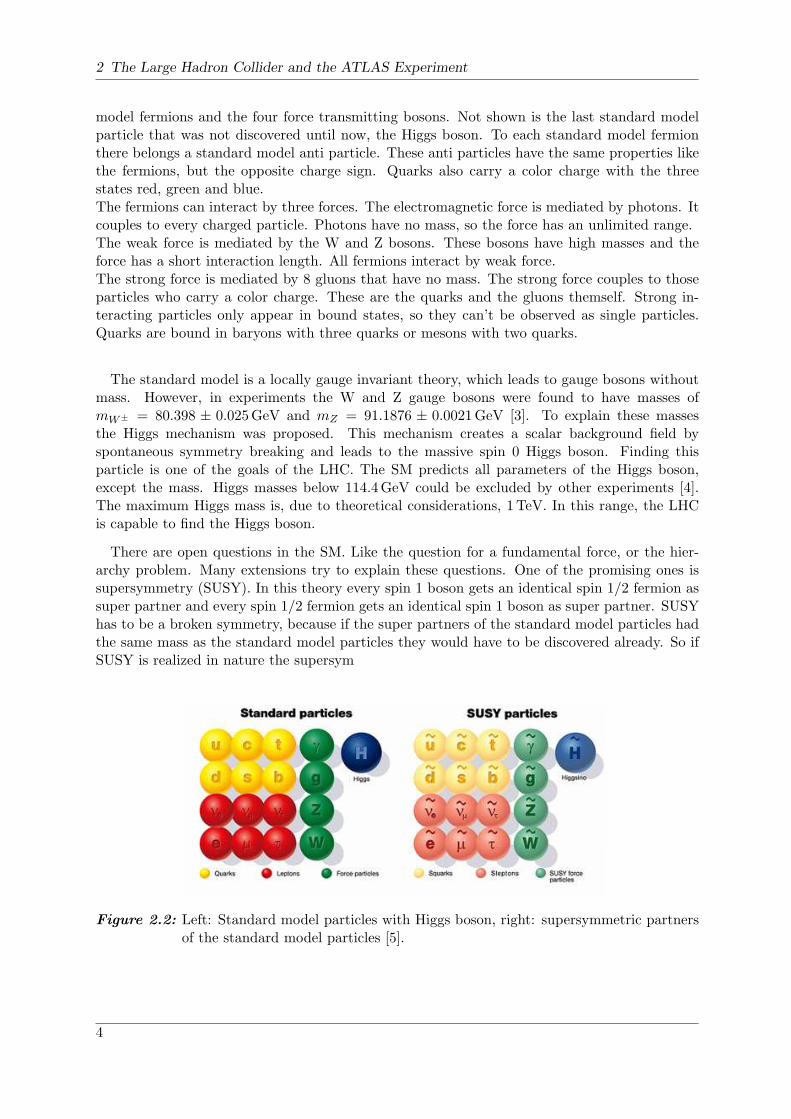
Figure 2.1: Overview on the standard model particles [2], the Higgs boson is not shown.
The fermions can be arranged in three generations. Most of the matter around us is builtup by particles from the first generation, like electrons or up and down quarks, which are theconstituents of neutrons and protons. The particles of the higher generations are much heavierthan these of the first generation and therefore not stable. Figure 2.1 shows the 12 standard
3
2 The Large Hadron Collider and the ATLAS Experiment
model fermions and the four force transmitting bosons. Not shown is the last standard modelparticle that was not discovered until now, the Higgs boson. To each standard model fermionthere belongs a standard model anti particle. These anti particles have the same properties likethe fermions, but the opposite charge sign. Quarks also carry a color charge with the threestates red, green and blue.The fermions can interact by three forces. The electromagnetic force is mediated by photons. Itcouples to every charged particle. Photons have no mass, so the force has an unlimited range.The weak force is mediated by the W and Z bosons. These bosons have high masses and theforce has a short interaction length. All fermions interact by weak force.The strong force is mediated by 8 gluons that have no mass. The strong force couples to thoseparticles who carry a color charge. These are the quarks and the gluons themself. Strong in-teracting particles only appear in bound states, so they can’t be observed as single particles.Quarks are bound in baryons with three quarks or mesons with two quarks.
The standard model is a locally gauge invariant theory, which leads to gauge bosons withoutmass. However, in experiments the W and Z gauge bosons were found to have masses ofmW± = 80.398 ± 0.025GeV and mZ = 91.1876 ± 0.0021GeV [3]. To explain these massesthe Higgs mechanism was proposed. This mechanism creates a scalar background field byspontaneous symmetry breaking and leads to the massive spin 0 Higgs boson. Finding thisparticle is one of the goals of the LHC. The SM predicts all parameters of the Higgs boson,except the mass. Higgs masses below 114.4GeV could be excluded by other experiments [4].The maximum Higgs mass is, due to theoretical considerations, 1TeV. In this range, the LHCis capable to find the Higgs boson.
There are open questions in the SM. Like the question for a fundamental force, or the hier-archy problem. Many extensions try to explain these questions. One of the promising ones issupersymmetry (SUSY). In this theory every spin 1 boson gets an identical spin 1/2 fermion assuper partner and every spin 1/2 fermion gets an identical spin 1 boson as super partner. SUSYhas to be a broken symmetry, because if the super partners of the standard model particles hadthe same mass as the standard model particles they would have to be discovered already. So ifSUSY is realized in nature the supersym
Figure 2.2: Left: Standard model particles with Higgs boson, right: supersymmetric partnersof the standard model particles [5].
4
2.2 The Large Hadron Collider
2.2 The Large Hadron Collider
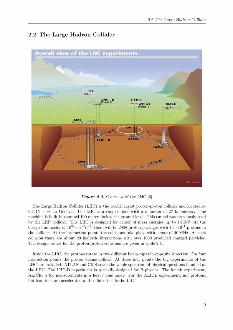
Figure 2.3: Overview of the LHC [6].
The Large Hadron Collider (LHC) is the world largest proton-proton collider and located atCERN close to Geneva. The LHC is a ring collider with a diameter of 27 kilometers. Themachine is built in a tunnel 100 meters below the ground level. This tunnel was previously usedby the LEP collider. The LHC is designed for center of mass energies up to 14TeV. At thedesign luminosity of 1034 cm−2s−1, there will be 2808 proton packages with 1.1 · 1011 protons inthe collider. At the interaction points the collisions take place with a rate of 40MHz. At eachcollision there are about 20 inelastic interactions with over 1000 produced charged particles.The design values for the proton-proton collisions are given in table 2.1.
Inside the LHC, the protons rotate in two different beam pipes in opposite direction. On fourinteraction points the proton beams collide. At these four points the big experiments of theLHC are installed. ATLAS and CMS cover the whole spectrum of physical questions handled atthe LHC. The LHC-B experiment is specially designed for B-physics. The fourth experiment,ALICE, is for measurements in a heavy ions mode. For the ALICE experiment, not protons,but lead ions are accelerated and collided inside the LHC.
5
2 The Large Hadron Collider and the ATLAS Experiment
ring circumference 26658.883m
magnet field strength 8.33T
bending radius 2803.95m
number of proton packages 2808
protons per package 1.1 · 1011distance of packages 25 ns
collision rate 40MHz
design luminosity 1034 cm−2s−1
Table 2.1: Design parameters of the LHC in proton-proton mode [7].
Until the end of 2010 the LHC has reached a luminosity of 2 · 1032 cm−2s−1. The maximalnumber of bunches inside the collider has been 368 [8].There are different upgrade possibilities for the LHC. One possibility is to increase the designluminosity from 1034 cm−2s−1 by a factor of ten to 1035 cm−2s−1. Another possibility is toincrease the center of mass energy by a factor of two to 24GeV. The second possibility is themore complicated and much more expensive one, so the first one is favored [9].
2.3 The ATLAS Experiment
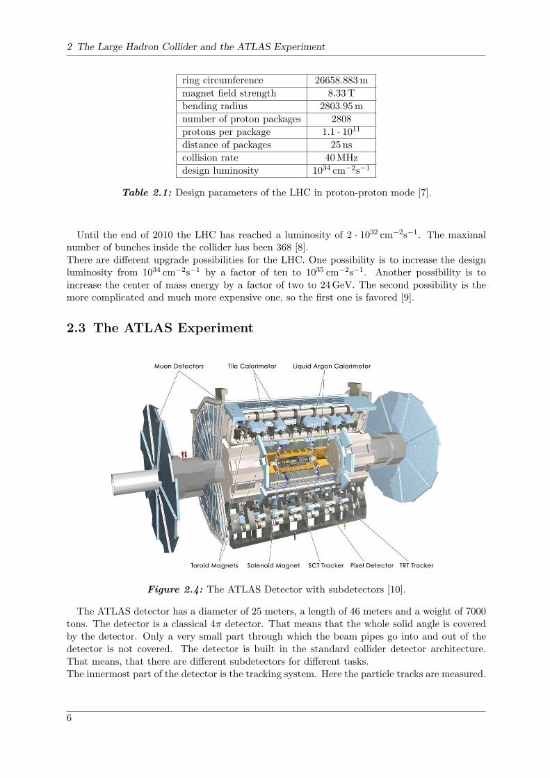
Figure 2.4: The ATLAS Detector with subdetectors [10].
The ATLAS detector has a diameter of 25 meters, a length of 46 meters and a weight of 7000tons. The detector is a classical 4π detector. That means that the whole solid angle is coveredby the detector. Only a very small part through which the beam pipes go into and out of thedetector is not covered. The detector is built in the standard collider detector architecture.That means, that there are different subdetectors for different tasks.The innermost part of the detector is the tracking system. Here the particle tracks are measured.
6
2.3 The ATLAS Experiment
The tracking system consists of three subdetectors. The innermost one is a semiconductor pixeldetector. It is followed by a silicon microstrip detector (SCT) and a transition radiation tracker(TRT). The inner detector system is surrounded by a solenoid magnet, so transverse momentumcan be measured with the tracking system.The next part of the detector is the calorimeter system. Here the particles are stopped and theirenergy is measured. The calorimeter system consists of two subdetectors, the electromagneticcalorimeter and the hadronic calorimeter.The outermost part of the ATLAS detector is the muon system. It consists of a huge toroidmagnet and a muon tracker. Muons are the only charged particles that can leave the calorime-ter system. With the magnetic field and the muon tracker the momentum of the muons can bemeasured.With this detector structure different goals can be reached. Because of the 4π geometry thewhole event can be detected and missing transverse energy1 can be related to neutrinos or newunknown particles. Because of the huge volume of the muon tracking system a precise mea-surement of the muon momentum is possible. With the inner detector system a very precisetracking is possible. Furthermore, the interaction point can be located very precisely.
2.3.1 The Inner Detector and the Solenoid Magnet
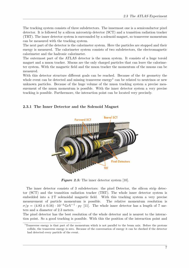
Figure 2.5: The inner detector system [10].
The inner detector consists of 3 subdetectors: the pixel Detector, the silicon strip detec-tor (SCT) and the transition radiation tracker (TRT). The whole inner detector system isembedded into a 2T solenoidal magnetic field. With this tracking system a very precisemeasurement of particle momentum is possible. The relative momentum resolution isσ/p = (4.83 ± 0.16) · 10−4GeV−1 · pT [11]. The whole inner detector has a length of 7 me-ters and a diameter of 2.3 meters.The pixel detector has the best resolution of the whole detector and is nearest to the interac-tion point. So a good tracking is possible. With this the position of the interaction point and
1Transverse energy is that part of the momentum which is not parallel to the beam axis. Before the protonscollide, the transverse energy is zero. Because of the conversation of energy it can be checked if the detectorhad detected every particle of the event.
7
2 The Large Hadron Collider and the ATLAS Experiment
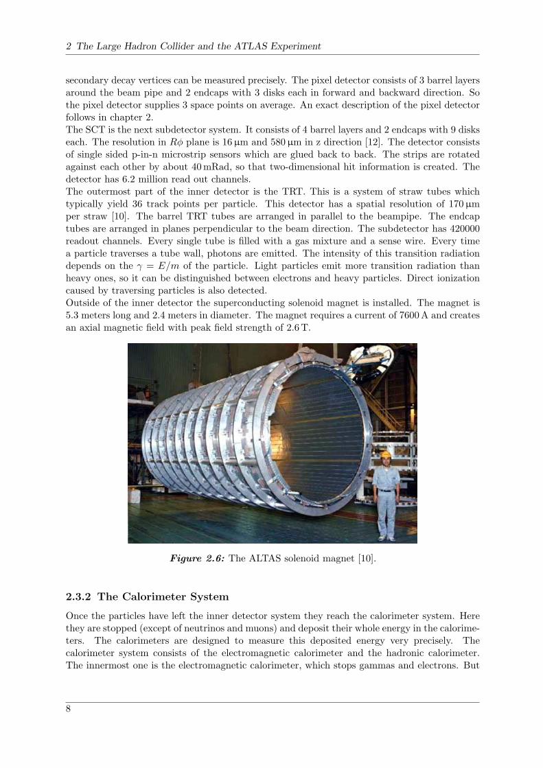
secondary decay vertices can be measured precisely. The pixel detector consists of 3 barrel layersaround the beam pipe and 2 endcaps with 3 disks each in forward and backward direction. Sothe pixel detector supplies 3 space points on average. An exact description of the pixel detectorfollows in chapter 2.The SCT is the next subdetector system. It consists of 4 barrel layers and 2 endcaps with 9 diskseach. The resolution in Rφ plane is 16µm and 580µm in z direction [12]. The detector consistsof single sided p-in-n microstrip sensors which are glued back to back. The strips are rotatedagainst each other by about 40mRad, so that two-dimensional hit information is created. Thedetector has 6.2 million read out channels.The outermost part of the inner detector is the TRT. This is a system of straw tubes whichtypically yield 36 track points per particle. This detector has a spatial resolution of 170µmper straw [10]. The barrel TRT tubes are arranged in parallel to the beampipe. The endcaptubes are arranged in planes perpendicular to the beam direction. The subdetector has 420000readout channels. Every single tube is filled with a gas mixture and a sense wire. Every timea particle traverses a tube wall, photons are emitted. The intensity of this transition radiationdepends on the γ = E/m of the particle. Light particles emit more transition radiation thanheavy ones, so it can be distinguished between electrons and heavy particles. Direct ionizationcaused by traversing particles is also detected.Outside of the inner detector the superconducting solenoid magnet is installed. The magnet is5.3 meters long and 2.4 meters in diameter. The magnet requires a current of 7600A and createsan axial magnetic field with peak field strength of 2.6T.
Figure 2.6: The ALTAS solenoid magnet [10].
2.3.2 The Calorimeter System
Once the particles have left the inner detector system they reach the calorimeter system. Herethey are stopped (except of neutrinos and muons) and deposit their whole energy in the calorime-ters. The calorimeters are designed to measure this deposited energy very precisely. Thecalorimeter system consists of the electromagnetic calorimeter and the hadronic calorimeter.The innermost one is the electromagnetic calorimeter, which stops gammas and electrons. But
8
2.3 The ATLAS Experiment
also hadrons deposit a little energy here while they cross the electromagnetic calorimeter. Theelectromagnetic calorimeter is a liquid argon calorimeter built in sampling architecture. Lead isused as absorber.The hadronic calorimeter is for the measurement of hadron energies. It is a sampling calorimeter,too, but with steal as absorber and plastic scintillators as active medium. Both calorimeters areapproximately 20 interaction lengths2 thick, so nearly all particles are stopped in the calorime-ters.
2.3.3 The Muon Chambers and the Toroid Magnet
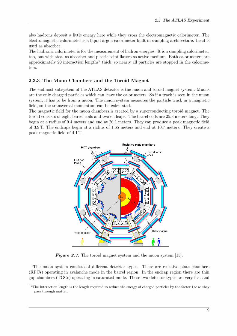
The endmost subsystem of the ATLAS detector is the muon and toroid magnet system. Muonsare the only charged particles which can leave the calorimeters. So if a track is seen in the muonsystem, it has to be from a muon. The muon system measures the particle track in a magneticfield, so the transversal momentum can be calculated.The magnetic field for the muon chambers is created by a superconducting toroid magnet. Thetoroid consists of eight barrel coils and two endcaps. The barrel coils are 25.3 meters long. Theybegin at a radius of 9.4 meters and end at 20.1 meters. They can produce a peak magnetic fieldof 3.9T. The endcaps begin at a radius of 1.65 meters and end at 10.7 meters. They create apeak magnetic field of 4.1T.
Figure 2.7: The toroid magnet system and the muon system [13].
The muon system consists of different detector types. There are resistive plate chambers(RPCs) operating in avalanche mode in the barrel region. In the endcap region there are thingap chambers (TGCs) operating in saturated mode. These two detector types are very fast and
2The Interaction length is the length required to reduce the energy of charged particles by the factor 1/e as theypass through matter.
9
2 The Large Hadron Collider and the ATLAS Experiment
used for triggering. For high resolution measurements drift tubes (MDTs) are used for a pseudo-rapidity3 smaller than two. These MDTs are drift chambers made of aluminum and filled witha gas mixture that survives high doses of radiation without aging. In the pseudorapidity regionbetween 2 and 2.7 cathode strip chambers (CSCs) are used. These are multi-wire proportionalchambers. The MDTs and CSCs have a spatial resolution of approximately 50µm.
3Pseudorapidity η is defined as η = ln tan θ2. θ is the polar angle of the particle relative to the beam line.
10
3 The Pixel Detector
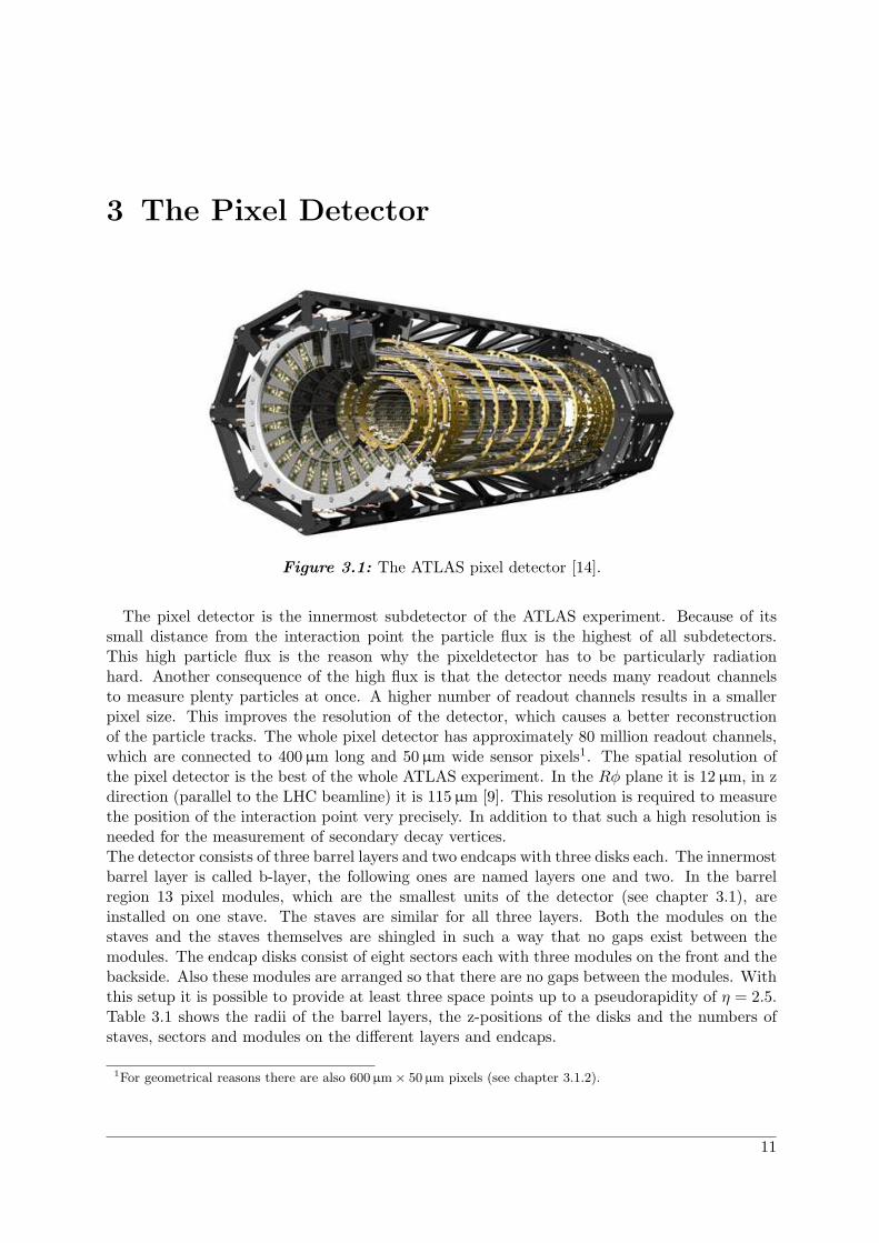
Figure 3.1: The ATLAS pixel detector [14].
The pixel detector is the innermost subdetector of the ATLAS experiment. Because of itssmall distance from the interaction point the particle flux is the highest of all subdetectors.This high particle flux is the reason why the pixeldetector has to be particularly radiationhard. Another consequence of the high flux is that the detector needs many readout channelsto measure plenty particles at once. A higher number of readout channels results in a smallerpixel size. This improves the resolution of the detector, which causes a better reconstructionof the particle tracks. The whole pixel detector has approximately 80 million readout channels,which are connected to 400µm long and 50µm wide sensor pixels1. The spatial resolution ofthe pixel detector is the best of the whole ATLAS experiment. In the Rφ plane it is 12µm, in zdirection (parallel to the LHC beamline) it is 115µm [9]. This resolution is required to measurethe position of the interaction point very precisely. In addition to that such a high resolution isneeded for the measurement of secondary decay vertices.The detector consists of three barrel layers and two endcaps with three disks each. The innermostbarrel layer is called b-layer, the following ones are named layers one and two. In the barrelregion 13 pixel modules, which are the smallest units of the detector (see chapter 3.1), areinstalled on one stave. The staves are similar for all three layers. Both the modules on thestaves and the staves themselves are shingled in such a way that no gaps exist between themodules. The endcap disks consist of eight sectors each with three modules on the front and thebackside. Also these modules are arranged so that there are no gaps between the modules. Withthis setup it is possible to provide at least three space points up to a pseudorapidity of η = 2.5.Table 3.1 shows the radii of the barrel layers, the z-positions of the disks and the numbers ofstaves, sectors and modules on the different layers and endcaps.
1For geometrical reasons there are also 600µm× 50µm pixels (see chapter 3.1.2).
11

3 The Pixel Detector
Radius (mm) No. of staves No. of modules
b-layer 55.5 22 286Layer one 88.5 38 494Layer two 122.5 52 676
z-position (mm) No. of sections No. of modules
Disk 1 ±495 8+8 48+48Disk 2 ±580 8+8 48+48Disk 3 ±650 8+8 48+48
Total 1744
Table 3.1: Setup and dimensions of the ATLAS Pixel detector [15].
3.1 The Pixel Module
The Pixel detector consists of 1744 pixel modules. They have a size of approximately 6.2×2 cm2.One module consists of a silicon sensor, the Front-End electronics and a copper-capton-flex board(see figure 3.2). Each sensor is connected to 16 equal Front-End chips (FE-chips) in such a waythat every sensor pixel has a link to its own read out cell.
Figure 3.2: Schematic view on the pixel module [16].
The connections between the sensor and the FE-chips are provided by little metal pelletscalled bump bonds. There are two different kinds of bump bonds, which are made of lead-tinor indium. The reason for the appearance of two different kinds of bonds is that the bondingof the sensors and the FE-chips was done by two different facilities, by using different methods.The two kinds of bonds show slightly different behaviours. The indium bonds have a diameterof approximately 20µm and a height of 8µm. They have a resistance of several ten ohms. The
12

3.1 The Pixel Module
lead-tin bonds have a spherical geometry with a diameter of 20µm and a resistance of less thanone ohm [17].On the back side of the sensor, the copper-capton-flex board is installed. The FE-chips and theflex board are connected with wire bonds that are located at the long edges of the module (seefigure 3.2). On the board the Module Control Chip (MCC) is installed. This chip gathers hitinformation from the FE-chips, processes them and sends them to the off detector electronics.For temperature measurements a negative temperature coefficient thermistor (NTC) is installedon the flex board. In the following the sensor, the FE-chip and the MCC are described in detail.
3.1.1 The Sensor
Silicon Semiconductor Detectors
Depleted pn junctions of semiconductors can be used for the detection of charged particles [18].When traversing a semiconductor, a charged particle deposits energy inside the material and,thereby, creates electron-hole pairs along the particle’s path. If there exists an electric field,these electron-hole pairs are separated and start drifting towards the read-out electrodes, wherethey induce an electrical signal. If the semiconductor is not depleted, the electron-hole pairswill recombine immediately, and the measurement of a signal will be impossible.The bandgap of silicon is 1.12 eV [19]. Because of lattice vibrations and stimulation the requiredaverage energy for the production of an electron-hole pair is increased to W = 3.62 eV [20].To calculate the mean energy loss 〈dE/dx〉 of a particle by traversing matter, the Bethe-Blochequation can be used. For traversing particles with a mass much bigger than the electron massthe energy loss is given by
−⟨
dE
dx
⟩
= 2πNar2emec
2ρZ
A
z2
β2·[
ln
(
2meγ2v2Wmax
I2− 2β2 − δ − 2
C
Z
)]
(3.1)
with:Na = 6.022 · 1023mol−1 is Avogadro’s number.re = 2.817 · 10−13 cm is the classical electron radius.me = 511 keV is the mass of an electron.ρ = 2.33 g/cm3 is the density of the absorbing material.I ≈ 173 eV is the average effective ionization potential.Z = 14 is the atomic number of the absorbing material.A = 28 is the atomic weight of the absorbing material.z is the charge of the traversing particles in units of e.β = v/c is the speed of the traversing particle in terms of the light speed c.γ = 1/
√
1− β2.δ is the density correction. It is important for higher energies and depends on the density of thetraversing material.C is the shell correction. It reduces the energy loss at lower energies and occurs with the wrongassumption that there are stationary electrons inside the material.Wmax = 2mec
2β2γ2 is the maximum energy transfer in a single head on head collision (forM >> me).
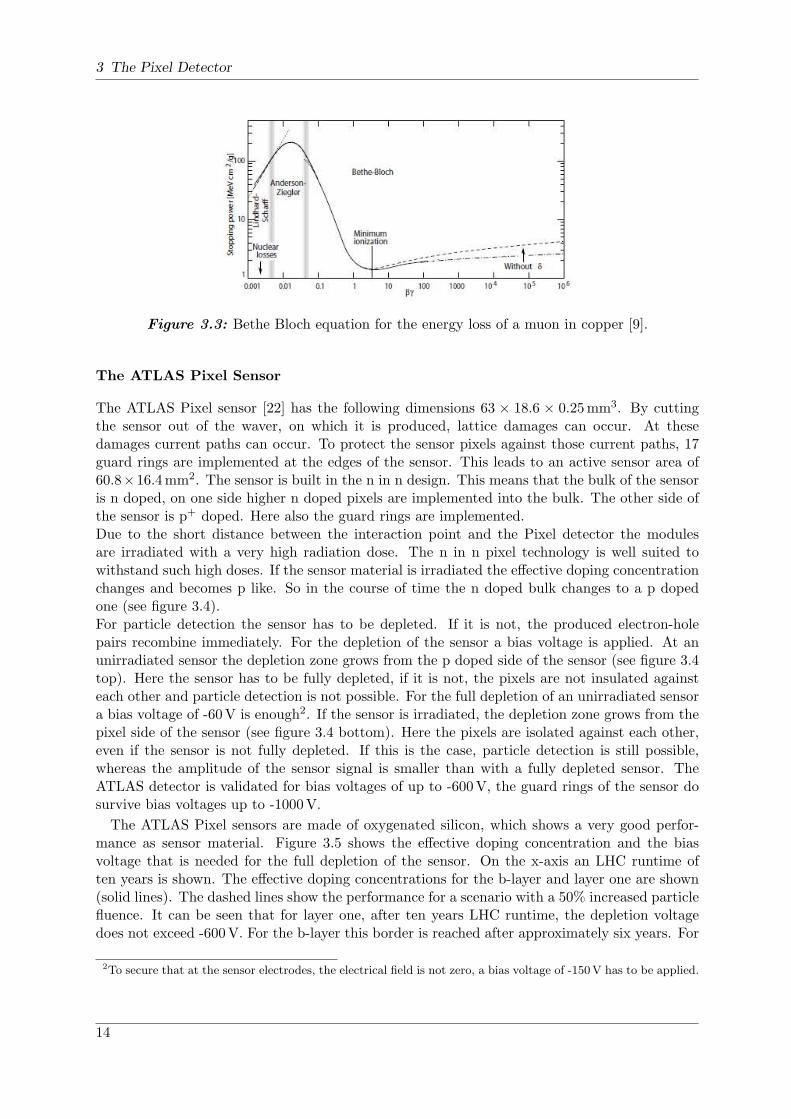
The shown formula is valid down to βγ ≈ 0.1. Its minimum is at βγ ≈ 3.5. Particles withcorresponding or higher βγ are called minimum ionizing particles (MIPs). An example for theBethe-Bloch equation is given in figure 3.3. In 250µm silicon the average energy loss of a MIPis approximately 69.9 keV, which corresponds 19300 electron hole pairs [21].
13
3 The Pixel Detector
Figure 3.3: Bethe Bloch equation for the energy loss of a muon in copper [9].
The ATLAS Pixel Sensor
The ATLAS Pixel sensor [22] has the following dimensions 63 × 18.6 × 0.25mm3. By cuttingthe sensor out of the waver, on which it is produced, lattice damages can occur. At thesedamages current paths can occur. To protect the sensor pixels against those current paths, 17guard rings are implemented at the edges of the sensor. This leads to an active sensor area of60.8×16.4mm2. The sensor is built in the n in n design. This means that the bulk of the sensoris n doped, on one side higher n doped pixels are implemented into the bulk. The other side ofthe sensor is p+ doped. Here also the guard rings are implemented.Due to the short distance between the interaction point and the Pixel detector the modulesare irradiated with a very high radiation dose. The n in n pixel technology is well suited towithstand such high doses. If the sensor material is irradiated the effective doping concentrationchanges and becomes p like. So in the course of time the n doped bulk changes to a p dopedone (see figure 3.4).For particle detection the sensor has to be depleted. If it is not, the produced electron-holepairs recombine immediately. For the depletion of the sensor a bias voltage is applied. At anunirradiated sensor the depletion zone grows from the p doped side of the sensor (see figure 3.4top). Here the sensor has to be fully depleted, if it is not, the pixels are not insulated againsteach other and particle detection is not possible. For the full depletion of an unirradiated sensora bias voltage of -60V is enough2. If the sensor is irradiated, the depletion zone grows from thepixel side of the sensor (see figure 3.4 bottom). Here the pixels are isolated against each other,even if the sensor is not fully depleted. If this is the case, particle detection is still possible,whereas the amplitude of the sensor signal is smaller than with a fully depleted sensor. TheATLAS detector is validated for bias voltages of up to -600V, the guard rings of the sensor dosurvive bias voltages up to -1000V.
The ATLAS Pixel sensors are made of oxygenated silicon, which shows a very good perfor-mance as sensor material. Figure 3.5 shows the effective doping concentration and the biasvoltage that is needed for the full depletion of the sensor. On the x-axis an LHC runtime often years is shown. The effective doping concentrations for the b-layer and layer one are shown(solid lines). The dashed lines show the performance for a scenario with a 50% increased particlefluence. It can be seen that for layer one, after ten years LHC runtime, the depletion voltagedoes not exceed -600V. For the b-layer this border is reached after approximately six years. For
2To secure that at the sensor electrodes, the electrical field is not zero, a bias voltage of -150V has to be applied.
14

3.1 The Pixel Module
Figure 3.4: Growing of the depletion zone of a pixel before and after irradiation [23].
this reason it is planed to insert an additional b-layer after five years runtime3. The pixel mod-ules are designed for a radiation dose of 1015cm−2 neutron equivalent4. This is the calculateddose, which a module is exposed to at the end of the ATLAS lifetime.
Figure 3.5: Depletion voltage for oxygenated silicon (solid lines) as a function of the LHCoperation time. The dashed lines show the performance for a 50% increased particlefluence. Also shown is the effective doping concentration. The upper lines showthe b-layer, the lower ones layer one. [25].
The aging effects of the sensor are temperature dependent. Tests showed that the optimaloperating temperature for the sensor is -10C. At any time, thermal free charge carriers areproduced inside the sensor material. The number of these charge carriers, and with that also
3The insertable b-layer project (IBL).4”The 1MeV equivalent neutron fluence is the fluence of 1 MeV neutrons producing the same damage in adetector material as induced by an arbitrary particle fluence with a specific energy distribution” [24].
15
3 The Pixel Detector
the leakage current of the sensor, depends on T 3/2 [9]. This is the reason why cooling of thesensor reduces the leakage current. After the irradiation of a sensor, this becomes especiallyimportant, because then the leakage current is increased.If the sensor is warmed up from time to time, the material defects, which were created by theradiation, heal out. This effect is called annealing. If the sensor is warmed up too long, thesensor properties start getting worse again. To use this annealing effect, the sensor is warmedup once a year, during the LHC run pause for a couple of days. This annealing effect can beseen at the knees of figure 3.5.
3.1.2 The Front-End Chip
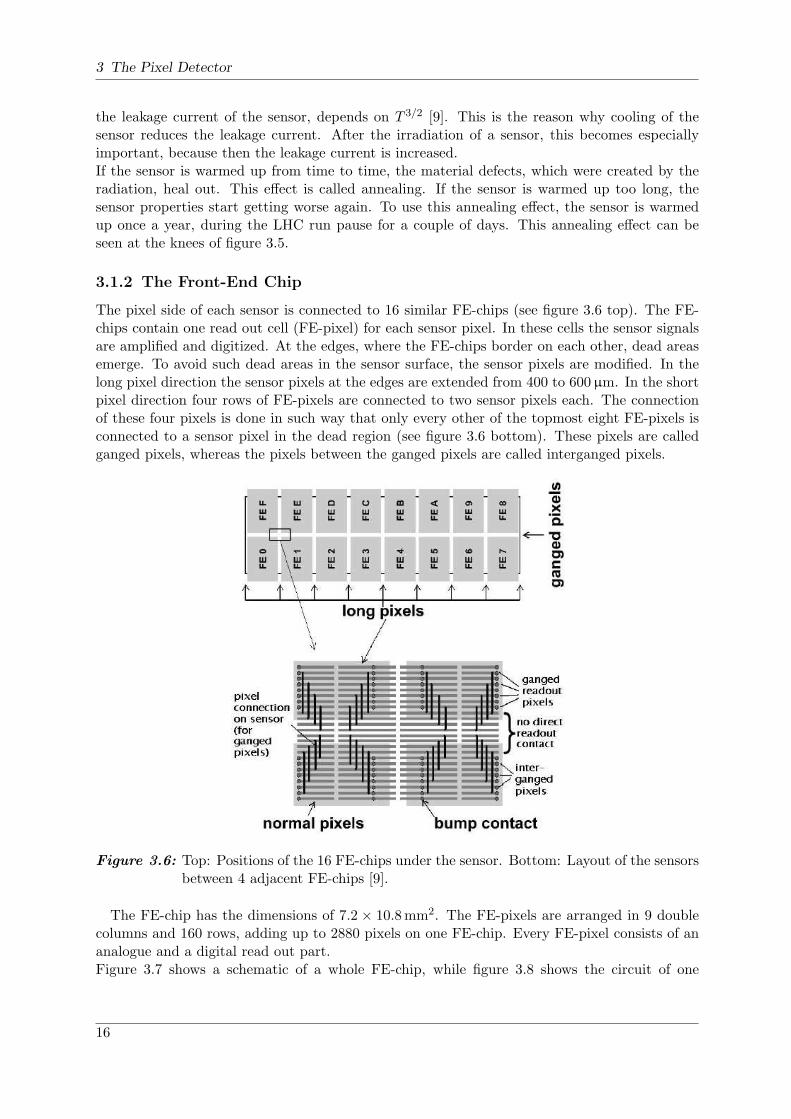
The pixel side of each sensor is connected to 16 similar FE-chips (see figure 3.6 top). The FE-chips contain one read out cell (FE-pixel) for each sensor pixel. In these cells the sensor signalsare amplified and digitized. At the edges, where the FE-chips border on each other, dead areasemerge. To avoid such dead areas in the sensor surface, the sensor pixels are modified. In thelong pixel direction the sensor pixels at the edges are extended from 400 to 600µm. In the shortpixel direction four rows of FE-pixels are connected to two sensor pixels each. The connectionof these four pixels is done in such way that only every other of the topmost eight FE-pixels isconnected to a sensor pixel in the dead region (see figure 3.6 bottom). These pixels are calledganged pixels, whereas the pixels between the ganged pixels are called interganged pixels.
Figure 3.6: Top: Positions of the 16 FE-chips under the sensor. Bottom: Layout of the sensorsbetween 4 adjacent FE-chips [9].
The FE-chip has the dimensions of 7.2 × 10.8mm2. The FE-pixels are arranged in 9 doublecolumns and 160 rows, adding up to 2880 pixels on one FE-chip. Every FE-pixel consists of ananalogue and a digital read out part.Figure 3.7 shows a schematic of a whole FE-chip, while figure 3.8 shows the circuit of one
16
3.1 The Pixel Module
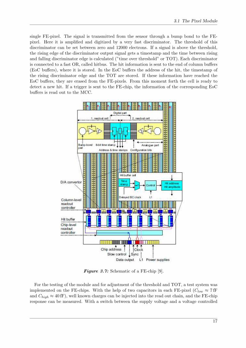
single FE-pixel. The signal is transmitted from the sensor through a bump bond to the FE-pixel. Here it is amplified and digitized by a very fast discriminator. The threshold of thisdiscriminator can be set between zero and 12000 electrons. If a signal is above the threshold,the rising edge of the discriminator output signal gets a timestamp and the time between risingand falling discriminator edge is calculated (”time over threshold” or TOT). Each discriminatoris connected to a fast OR, called hitbus. The hit information is sent to the end of column buffers(EoC buffers), where it is stored. In the EoC buffers the address of the hit, the timestamp ofthe rising discriminator edge and the TOT are stored. If these information have reached theEoC buffers, they are erased from the FE-pixels. From this moment forth the cell is ready todetect a new hit. If a trigger is sent to the FE-chip, the information of the corresponding EoCbuffers is read out to the MCC.
Figure 3.7: Schematic of a FE-chip [9].
For the testing of the module and for adjustment of the threshold and TOT, a test system wasimplemented on the FE-chips. With the help of two capacitors in each FE-pixel (Clow ≈ 7 fFand Chigh ≈ 40 fF), well known charges can be injected into the read out chain, and the FE-chipresponse can be measured. With a switch between the supply voltage and a voltage controlled
17
3 The Pixel Detector
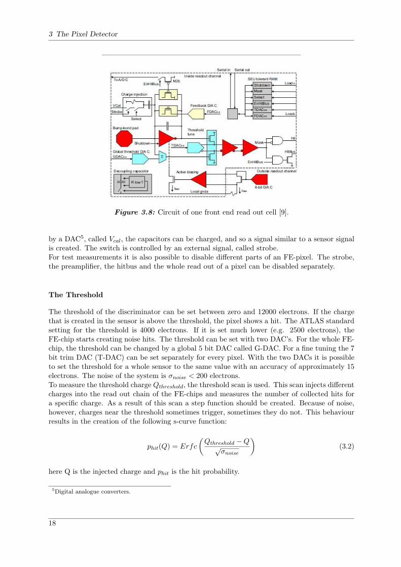
Figure 3.8: Circuit of one front end read out cell [9].
by a DAC5, called Vcal, the capacitors can be charged, and so a signal similar to a sensor signalis created. The switch is controlled by an external signal, called strobe.For test measurements it is also possible to disable different parts of an FE-pixel. The strobe,the preamplifier, the hitbus and the whole read out of a pixel can be disabled separately.
The Threshold
The threshold of the discriminator can be set between zero and 12000 electrons. If the chargethat is created in the sensor is above the threshold, the pixel shows a hit. The ATLAS standardsetting for the threshold is 4000 electrons. If it is set much lower (e.g. 2500 electrons), theFE-chip starts creating noise hits. The threshold can be set with two DAC’s. For the whole FE-chip, the threshold can be changed by a global 5 bit DAC called G-DAC. For a fine tuning the 7bit trim DAC (T-DAC) can be set separately for every pixel. With the two DACs it is possibleto set the threshold for a whole sensor to the same value with an accuracy of approximately 15electrons. The noise of the system is σnoise < 200 electrons.To measure the threshold charge Qthreshold, the threshold scan is used. This scan injects differentcharges into the read out chain of the FE-chips and measures the number of collected hits fora specific charge. As a result of this scan a step function should be created. Because of noise,however, charges near the threshold sometimes trigger, sometimes they do not. This behaviourresults in the creation of the following s-curve function:
phit(Q) = Erfc
(
Qthreshold −Q√σnoise
)
(3.2)
here Q is the injected charge and phit is the hit probability.
5Digital analogue converters.
18
3.1 The Pixel Module
Figure 3.9: Number of hits as a function of the Vcal value fitted with a s-curve [9].
Time over Threshold
The signal generated by the sensor is amplified by a charge sensitive preamplifier. This pream-plifier has a 10 fF feedback capacitor for charge collection, which is discharged by a constantcurrent source. The discharging current can be regulated by two DAC’s, a global 8 bit IF-DACand a 3 bit F-DAC that can be set separately for every pixel. By these two DAC’s a homoge-neous amplifier recovery time for the whole FE-chip is ensured.The recovery time of the amplifier, and with this the time over threshold of the discriminatoroutput, depends on the charge that is produced by the traversing particle. This dependency isapproximately linear [9]. So, with the IF-and F-DAC the TOT of the discriminator for a certaincharge can be adjusted. The benchmark value for a charge of 20000 electrons is a TOT of 30bunchcrossings. The described mechanism can be used for measuring the charge that a particlehas created by traversing the sensor. In chapter 4.3.1 the procedure of a TOT-charge calibrationis shown.
Timing and Timewalk
For reconstructing the particle track, it is necessary to ensure that the hits are associated withthe correct 25 ns LHC bunchcrossing. Figure 3.10 shows the timing during charge injection witha strobe signal. A certain time after the strobe signal is sent, the preamplifier output startsrising and the discriminator output rises from zero to one. If a trigger signal is sent, the eventcorresponding to the bunchcrossing, which has occurred earlier by a time span called latency,is read out to the MCC. The bunchcrossing, which corresponds to the correct hit, is markedin green. The latency originates in the time the trigger system needs to make a decision. Thetrigger delay is the time between the strobe signal and the trigger signal. It has to be set insuch way that the discriminator signal ends up in the correct acceptance window. One triggercan read out between one and 16 consecutive bunchcrossings. These bunchcrossings are labelledwith numbers from 0 to 15, which are called LV1ID. In the ALTAS detector this LV1ID windowis only one bunchcrossing long, because at every bunchcrossing collisions happen. For laboratorytests, however, it can be extended.The rise time of the preamplifier is charge dependent. Lower charges result in longer rise timesof the preamplifier, and with that in a later threshold crossing. If the collected charge is verysmall, it happens that the hit is not registered until the following bunchcrossing. This effect iscalled timewalk, it is illustrated in figure 3.11.
19
3 The Pixel Detector
Figure 3.10: Sketch of the pixel read-out timing [9].
Figure 3.11: Amplifier output and discriminator response for small and large charges.
3.1.3 The Module Control Chip
The module control chip processes the data coming from the 16 FE-chips and handles thecommunication between the module and the ATLAS data taking system [9]. It receives theconfiguration data and distributes it among the different FE-chips. It also creates and distributesdifferent reset and timing signals.When the MCC receives the trigger signal from the ATLAS trigger system, it initiates the datareadout from the FE-chips. The data is read out into 16 FIFO’s6, one for each FE-chip. With thewhole data set from the 16 FE-chips the event is built and provided with a timestamp. Then itis forwarded to the further read out electronic and transformed into a serial data stream. Finallythis data stream is sent to the ATLAS data taking system via two LVDS7 data lines.Another feature of the MCC is to test the read out chain between the FE-chips and the offdetector electronic. The configurations sent to the FE-chips can be read back from the FE-chips. From the outside, artificial events can be sent in combination with a trigger, to theFIFO’s, so the MCC data processing can be tested.
6First in first out buffers.7Low voltage differential signals.
20

3.2 The USB-Pix System
3.2 The USB-Pix System
For laboratory measurements an USB based test system was developed. With this system, whichconsists of a multi purpose IO-Board (S3MultiIO), an adapter card and a single chip module(see figure 3.12), it is possible to test the FE-chip and the sensor.
The Multi Purpose IO-Board
The Multi purpose IO-Board is equipped with a microcontroller with USB2.0 interface, anFPGA8 and an SRAM9 [26]. With the microcontroller the data transfer between the PC andthe Multi purpose IO-Board is handled. The FPGA provides and handles the signal transferto the FE-chip. Examples are: clock, trigger, reset signals or the configuration of the FE-chip.Moreover, it stores the data coming from the FE-chip on the 16Mbit SRAM.The Multi purpose IO-Board provides a large number of connections, like the 100 pin connectorfor the connection to the adapter card, or six LEMO connectors, which can be used for signalin or output.
Figure 3.12: Components of the USBPix laboratory test system [27].
The LEMO connectors provide access to different signals. The channel layout of the LEMOconnectors is set by the FPGA programming. The connectors are labeled with the names TX0,TX1, TX2, RX0, RX1 and RX2 (figure 3.12 from the left to the right). The connector TX2, forexample, is connected to the hitbus signal, whereas the connector RX0 is used as trigger input.
8Field Programmable Gate Array.9Static Random Access Memory.
21

3 The Pixel Detector
FE-I3 Adapter Card
The FE-I3 Adapter Card [28] is connected to the hundred pin connector of the Multi purposeIO-Board. It provides LVDS signal buffers and the digital and analogue supply voltages for theFE-chip.
Single Chip Card
Single chip cards are modules with only one FE-chip and a customized sensor, they do not havean MCC. A single chip card is connected to an adapter card via a flat ribbon cable. The sensorbias voltage is applied to a LEMO connector. The supply voltage for the LVDS drivers of thesingle chip card can be supplied via a LEMO connector or via the flat ribbon cable. Whichconnection is used is set with a solder bridge. The physical address of the card can also be setby 4 solder bridges, so addresses between 0 and 15 are possible. There are several pins on thesingle chip card to pick up different signals like the clock or the analogue and digital supplyvoltages. The FE-chip is glued on the single chip card and via wire bonds, connected to it. Forlaboratory tests single chip cards are produced both with and without a sensors.
22
4 The Laser System
With a laser it is possible to inject charges with high precision into the sensor. The position ofthe charge injection can be adjusted with an accuracy of less than one micrometer. Furthermore,the area, where the charge is injected, can be measured very precisely, because the diameter ofthe laser beamspot is well known. The injected charge can be modified easily by variation ofthe laser pulse intensity. Because of the high laser pulse frequency (up to 1MHz) it is possibleto reach a large number of charge injections in a very short time.With a laser system it is possible to inject charges in different positions at the sensor. So it ispossible to study the effects which appear at the edge of a pixel or at the edge of the wholesensor. With different laser wavelengths it is possible to inject charges only on the surface ofthe sensor or throughout the whole sensor thickness. Likewise, the time at which the laser pulseis injected can be controlled very precisely. With this, time response studies are possible.
4.1 Charge Injection via Laser Light
For the measurements of this study two lasers were available. One is an infrared laser with awavelength of 1060 nm, the other is a red laser with a wavelength of 671 nm. The pulse widthof the red laser is 31 ps. It has a peak power of 500mW. The infrared laser has a pulse width of41 ps and a peak power of 700mW.Most of the particles that are detected by the ATLAS pixel detector are MIPs. By traversingthe sensor they produce approximately 20000 electron-hole pairs (see chapter 3.1.1). For thesimulation of a MIP that traverses the sensor, the laser pulse energy, which is needed to createsuch a charge, has to be calculated. The average energy needed to create one electron-hole pairin silicon is W = 3.62 eV [20] (see chapter 3.1.1). Thus to create 20000 electron-hole pairs anenergy of E20000 = 20000 ·W = 63.2 keV is necessary.The energy of one laser pulse is Epulse = Pt, where t is the puls width and P the peak powerof the laser pulse. From the peak power, the corresponding peak energies Epeak can be cal-culated. The red laser’s peak energy is 106.1MeV. For the infrared laser it is 179.1MeV. Itis apparent that for the creation of a charge that corresponds to a MIP the lasers have to beattenuated. The attenuation a that is needed to create 20000 electron-hole pairs is calculated bya = Epulse/E20000 = Pt/E20000. For the red laser the attenuation was calculated as 1679, forthe infrared one as 2834.The energy of one photon is given by Eγ = hν = hc/λ, where λ is the wavelength of the laser.For the red laser it results Eγ,red=1.85 eV, for the infrared one Eγ,IR=1.17 eV. With these valuesthe number of photons that are needed to create 20000 electron-hole pairs could be calculaten20000 = E20000/Eγ . It became apparent that with the red laser 34000 photons are needed, withthe infrared laser the number of photons has to be 54000. Table 4.1 gives an overview of thecalculated values for the red and the infrared laser.
23
4 The Laser System
Wavelength, 671 nm 1060 nm
Photon energy, Eγ 1.85 eV 1.17 eV
Laser peakpower, P 500mW 700mW
Pulswidth, t 34 ps 41 ps
Nominal pulse energy, Epulse 106.1MeV 179,1MeV
Attenuation, a 1679 2834
Number of photons nγ for a MIP 34162 54017
Table 4.1: Electron-hole pair production with red and infrared laser light in silicon.
The intensity loss of light by traversing matter is calculated by
I(x) = I0 · e−αx (4.1)
Here α is the absorption coefficient, and x is the depth of the photon beam in matter. Theabsorption coefficient is frequency depended. This dependency is shown in Figure 4.1. It isapparent that the absorption coefficient gets smaller for higher frequencies. This results in thefact that the laser with a wavelength of 1060 nm penetrates the sensor more deeply than thelaser with a wavelength of 671 nm does. The red laser light enters into silicon approximately4µm deep [29], so the charge is only produced at the surface of the sensor. For infrared laserlight, at a 250µm thick silicon layer approximately 55% of the intensity are absorbed. 12% aretransmitted and 33% are reflected [30]. This shows that by using the infrared laser the chargeproduction happens throughout the whole sensor.
Figure 4.1: Absorption coefficient for silicon as a function of the wavelength [31].
4.2 Setup
The measurement setup has to fulfill different tasks: The laser beam has to be attenuated toadjust the correct laser intensity. It has to be divided to inject charges into the sensor and to
24
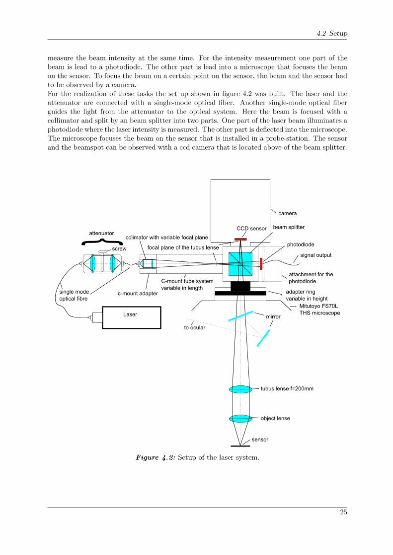
4.2 Setup
measure the beam intensity at the same time. For the intensity measurement one part of thebeam is lead to a photodiode. The other part is lead into a microscope that focuses the beamon the sensor. To focus the beam on a certain point on the sensor, the beam and the sensor hadto be observed by a camera.For the realization of these tasks the set up shown in figure 4.2 was built. The laser and theattenuator are connected with a single-mode optical fiber. Another single-mode optical fiberguides the light from the attenuator to the optical system. Here the beam is focused with acollimator and split by an beam splitter into two parts. One part of the laser beam illuminates aphotodiode where the laser intensity is measured. The other part is deflected into the microscope.The microscope focuses the beam on the sensor that is installed in a probe-station. The sensorand the beamspot can be observed with a ccd camera that is located above of the beam splitter.
to ocular
Laser
CCD sensor
adapter ring
variable in height
Mitutoyo FS70L
THS microscopemirror
camera
beam splitter
tubus lense f=200mm
object lense
sensor
focal plane of the tubus lense
C-mount tube system
variable in length
colimator with variable focal plane
c-mount adapterattenuator
screw
single mode
optical fibre
photodiode
attachment for the
photodiode
signal output
Figure 4.2: Setup of the laser system.
25
4 The Laser System
4.2.1 The Laser
As laser system the picoseconds injection laser (PiLas) from Advanced Laser Diode Systemswas used. This laser system consists of a control unit and two diode laser heads (671 nm and1060 nm). Both lasers are class one lasers. All measurements in this thesis were made with thered 671 nm laser.The laser pulse repetition frequency can be adjusted between 10Hz and 1MHz. The laser pulsefrequency jitters about 3 - 4 ps [32]. The controller allows manual and external triggering of thelaser pulses. If the laser is triggered externally, the jitter of the optical output depends on theslope quality and the noise of the trigger’s source [32]. For triggering a TTL1 signal or a NIM2
signal can be used. The trigger level can also b adjusted between -5V and 5V [32].As the performance of the laser diode is temperature dependent, the laser system needs 15minutes warm up time to reach a thermal equilibrium. With a temperature change of 1K, thetime of the laser pulse emission can change by up to 10 ps [32]. The laser intensity can be setby a TUNE value between 1 and 100%.
Laser Pulse Frequency Dependence of the Laser Intensity
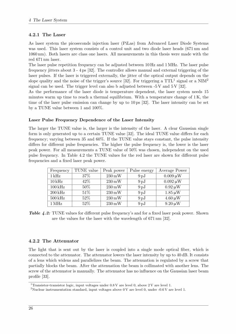
The larger the TUNE value is, the larger is the intensity of the laser. A clear Gaussian singleform is only generated up to a certain TUNE value [32]. The ideal TUNE value differs for eachfrequency; varying between 35 and 60%. If the TUNE value stays constant, the pulse intensitydiffers for different pulse frequencies. The higher the pulse frequency is, the lower is the laserpeak power. For all measurements a TUNE value of 50% was chosen, independent on the usedpulse frequency. In Table 4.2 the TUNE values for the red laser are shown for different pulsefrequencies and a fixed laser peak power.
Frequency TUNE value Peak power Pulse energy Average Power
1 kHz 37% 230mW 9pJ 0.009µW
10kHz 42% 230mW 9pJ 0.092µW
100 kHz 50% 230mW 9pJ 0.92µW
200 kHz 51% 230mW 9pJ 1.85µW
500 kHz 52% 230mW 9pJ 4.60µW
1MHz 52% 230mW 9pJ 9.20µW
Table 4.2: TUNE values for different pulse frequency’s and for a fixed laser peak power. Shownare the values for the laser with the wavelength of 671 nm [32].
4.2.2 The Attenuator
The light that is sent out by the laser is coupled into a single mode optical fiber, which isconnected to the attenuator. The attenuator lowers the laser intensity by up to 40 dB. It consistsof a lens which widens and parallelizes the beam. The attenuation is regulated by a screw thatpartially blocks the beam. After the attenuation the beam is collimated with another lens. Thescrew of the attenuator is manually. The attenuator has no influence on the Gaussian laser beamprofile [33].
1Transistor-transistor logic, input voltages under 0.8V are level 0, above 2V are level 1.2Nuclear instrumentation standard, input voltages above 0V are level 0, under -0.6V are level 1.
26
4.2 Setup
4.2.3 Optical System
For the focusing and splitting of the laser beam a system consisting of various optical componentswas used. To focus the beam on the sensor and to minimize the beamspot diameter, these opticalcomponents had to be adjusted.
Laser Collimator
The single mode optical fiber coming from the attenuator is connected to a laser collimator.This collimator is used for the focusing and collimation of the laser beam. The diameter of thebeamspot depends on the adjustment of the laser collimator. The smallest beamspot is obtainedif the focal plane of the collimator is the same as the focal plane of the microscope’s lens tube(see figure 4.2).The adjustment of the collimator is done via a little screw on top of the collimator. Subsequently,the focal plane is changed by rotating the screw until the beamspot is minimal. This calibrationhas to be redone when a different laser is used. The position of the focal plane of the lens tubedepends on the reflection index of the lens tube which in turn is wavelength dependent.
C-Mount System
To connect the collimator with the beam splitter a c-mount3 system from ”Linos” was used.The focal plane of the lens tube is 17.5mm in front of the beam splitter. The focal length of thecollimator has to be in the same order as the focal length of the tube lens. If the focal lengthof the collimator is too short, the laser beam is fanned out too much and it is reflected at themicroscope walls. If the focal length is too long, the beam is very small and the objective lensis not fully illuminated. As distance between the focal plane of the tube lens and the collimatorthe focal length of the tube lens, which is 200mm, was chosen. Thus the c-mount structurebetween the collimator and the beam splitter had to have a length of 217mm.For its adjustment the c-mount system can be extended or shortened by screwing two parts ofthe system into each other.
Beam Splitter
The beam splitter is the part which connects the microscope, the camera, the photodiode andthe collimator via c-mount connections. It splits the incoming beam into two parts. One partgoes through the cube and the other part is deflected by 90. In this process the beam is splitin the ratio of one to one. The transmitted part of the laser beam is guided to the photodiode,where the laser intensity is measured. The reflected part is sent through an adapter ring intothe microscope.The laser beam has to be redirected in such way that it is parallel to the optical axis of themicroscope. This could be accomplished by changing the angle between the beam splitter andthe optical axis of the microscope. Only if this angle is set very precisely, is the laser beamspotin the middle of the observed picture. If this angle is set up badly, the laser beam would notreach the objective lens. The angel of the beam splitter can be adjusted with six little screwson the support structure of the beam splitter.
3The c-mount standard defines the parameters of the threads of optical components.
27
4 The Laser System
Camera
The pictures viewed by the microscope are monitored with a Sony CCD black and white videocamera module XC-ST50 CE. This camera has a c-mount connection so that it can be installedeasily on the beam splitter. The resolution of the camera is 768 × 494 pixels [34]. The camerais sensitive in infrared and visible wavelengths. In this way also the infrared laser beamspot canbe observed.
Camera Adapter Ring
The camera adapter ring is located between the beam splitter and the camera input of themicroscope. It is variable in height. With this ring the sensor of the ccd camera can be broughtinto the focal plane of the tube lens. If the camera is not in the focal plane of the tube lens,it becomes necessary to refocus the microscope when switching between observation by cameraand by ocular. For the adjustment of the focal plane, the adapter is adjustable about 10mm inheight.
The Microscope
For observing and focusing the beamspot on the sensor a Mitutoyo FS70L THS microscope isused. The microscope is equipped with 4 different objectives with magnifications of 2×, 10×,20× and 50×. Moreover, a connection for the installation of a camera is available. Here thebeam splitter is installed. For observation, the light can be switched between the ocular and thecamera output. Having a picture on both outputs at the same time is not possible. The focalplane of the tube lens is 79.6mm above the camera output.The microscope is mounted on the probe-station. It can be moved in all three directions. In xand y direction the resolution is 0.25µm, in z direction 0.1µm [35].The 20× and 50× objectives generate beamspots that are small enough to inject charges onlyin one pixel (see chapter 4.4.2). Because of problems with the installation of the 50× objectiveonly the 20× objective was used for the measurements.
4.2.4 The Probe-Station
The probe-station PA300 from Suss MicroTec consists of a chuck that can be cooled and a casearound this chuck. The microscope is installed on top of this case. It can be lifted, so thatit is possible to install hardware under the microscope. There are also other covers for theinstallation of hardware. The chuck could be driven in all three directions. In x and y directionthe precision of the chuck is 0.5µm, in z direction it is 0.25µm [35]. The chuck temperature canbe adjusted between -55C and 160C. The accuracy of the set temperature is 0.5C [36]. Itis possible to flush the case with dry air, so condensation can be prevented. A safety interlocksystem was installed at the probe-station. This interlock ensures that people cannot come incontact with the laser beam.
Safety Interlock System
The whole system, from the laser collimator via the microscope through to the chuck, is lightproof. So the user cannot get in contact with laser light. To ensure that the laser cannot beswitched on while the microscope is lifted or while one of the covers is opened, an interlocksystem was installed. The interlock consists of different switches that are connected in series. Ifone of these switches is opened, the power connection of the laser control unit is interrupted.
28
4.2 Setup
The microscopes light path can be switched between the camera and the ocular by hand. Thistoggles a switch, which is closed when the light path is conducted to the camera position.Otherwise, if the light path is conducted to the ocular position, the switch is opened. So it isguarantied that it is not possible to look through the ocular into the laser beam. In this interlockcircuit an additional hand switch is installed. It is used as remote control for the laser.
Temperature Monitoring
For the installation of a single chip card and to ensure good thermal contact between the sen-sor and the chuck a fixing structure was constructed. For temperature monitoring a negativetemperature coefficient resistor (NTC)4 is installed within this structure. In this way the tem-perature very close to the sensor can be measured. The NTC is read out by a digital multimeter.At the nominal temperature T0 = 25C the NTC has a resistance of R0 = 2kΩ. The temperaturerange of the NTC extends from -60C to +150C. The tolerance is 0.5% and the characteristicalB-value is 3976K [37]. The temperature T can be calculated by measuring the resistance R:
T =B · T0
B + ln(
RR0
)
· T0
(4.2)
4.2.5 The Photodiode
The photodiode is installed on the beam splitter. It measures the laser intensity of the trans-mitted part of the beam. The output voltage of the photodiode is linearly dependent on thelaser intensity [38]. So the relation between the photovoltage and the laser intensity under themicroscope can be calibrated easily. Thus it is possible to set up the right laser intensity at theattenuator.For the measurement of the laser intensity a S9269 silicon photodiode with amplifier from Hama-matzu was used. This diode has an active area of 5.8 × 5.8mm2. It is sensitive to visible andnear infrared light. For a wavelength of 671 nm the photosensitivity is about 0.43 V
nW. For a
wavelength of 1060 nm it is about 0.20 V
nW[38].
The preamplifier of the diode needs a supply voltage of U± = ±15V. The signal output of thediode is connected to an Agilent 34410A Digital Multimeter, which measures the output voltageof the diode. There is a strong laser pulse frequency dependence of the output voltage. This de-pendency is due to three reasons: First of all, the response of the photodiode changes by varyingthe frequency of the incoming light (see above). Secondly, the laser intensity itself is frequencydependent (see chapter 4.2.1). And finally, the photodiode measures the average intensity ofthe laser beam and not the pulse intensity. The average intensity depends on the laser pulsefrequency, so if the pulse frequency is lowered by about a factor of 10, the photovoltage will alsobe lowered about a factor of 10.Because of this frequency dependency it is difficult to do measurements at low laser pulse fre-quencies, because in that case the output voltage of the photodiode gets too low.The output voltage of the photodiode ranges between 0 and 15V. Photovoltages down to 1mVcan be measured reliably.
4NTC-Temp-Sensor TS-NTC-202-60/+150C.
29
4 The Laser System
4.3 Calibration
For the calibration of the correlation between the photovoltage and the charge that is injectedinto the sensor the unirradiated sensor 11-5B was used. The threshold was tuned to 3200electrons and for each measurement 50000 laser pulses were injected into the sensor. For thecalibration, the TOT response was measured for several laser intensities, which were chosen insuch a way that the whole voltage range of the photodiode (1mV to 15V) was covered. Fromthe TOT values the corresponding charges could be calculated and the charge-photovoltage cal-ibration could be done. Because of the laser pulse frequency dependency of the photovoltage,this calibration had to be done separately for each pulse frequency. The different object lenseshave different reflection indexes, so the calibration had to be done, for each objective. Thecalibration shown here was done with the 20× objective.For all calibration measurements the laser beam was focused on the pixel with the columnnumber 9 and the row number 13 (pixel 9/13). For small charges (up to approximately 50000electrons) the beamspot was smaller than 50µm and only the targeted pixel showed hits. Forlarger charges also the neighbor pixels showed hits. For the calibration measurement all pixelswere disabled, except for a small cluster around that pixel in which the charge was injected. Sothe noise could be minimized.The photodiode calibration was split into two parts. The first part was the TOT-charge cali-bration of the FE-I3 readout chip. In this process the charge values were calculated from theTOT values. The second part was the photovoltage calibration itself. In this process the photo-voltage was measured with the multimeter and the TOT was measured with the silicon sensor.With the TOT-charge calibration and the photovoltage-TOT calibration the relation betweenthe photovoltage and the injected charge could be calibrated.
4.3.1 TOT-Charge Calibration
For the TOT-charge calibration a TOT-Calib scan was done. Well known charges were injected50 times into each pixel and the TOT response was measured. This measurement was donewith 54 different injection charges for each capacitor. The TOT-charge calibration was doneseparately for each pixel.To inject a charge into a pixel, a capacitor (Clow or Chigh) was charged by a voltage pulse.The height of this voltage pulse was calculated by multiplying the Vcal −DAC with the voltagedifference ∆V between two Vcal −DAC values5.
U = Vcal ·∆V (4.3)
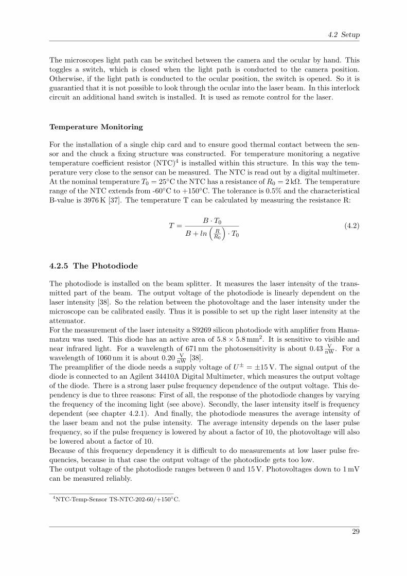
The injected charge is calculated by Q = C ·U . For each module an average capacitance wasmeasured at the module assembly. These capacities were not very precise and by calculatingthe charges from the Vcal values a step was seen between the curves of the two capacities (seefigure 4.3). To improve the calibration the capacities Clow and Chigh were calculated separatelyfor every pixel.
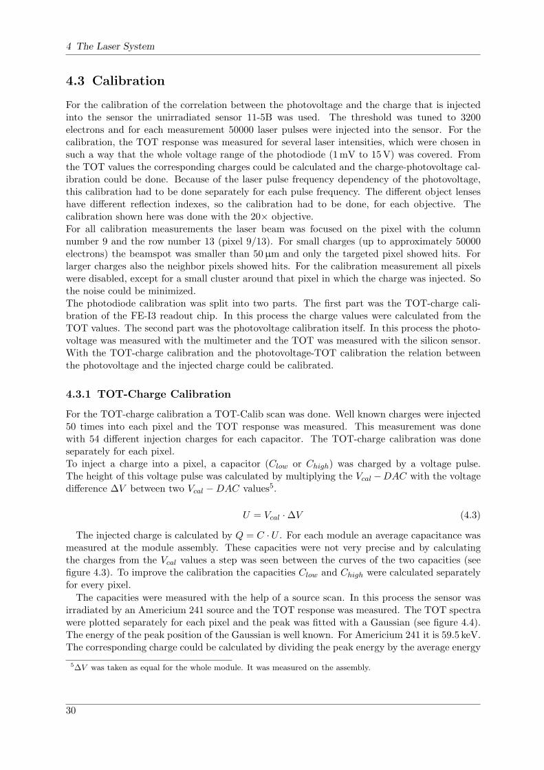
The capacities were measured with the help of a source scan. In this process the sensor wasirradiated by an Americium 241 source and the TOT response was measured. The TOT spectrawere plotted separately for each pixel and the peak was fitted with a Gaussian (see figure 4.4).The energy of the peak position of the Gaussian is well known. For Americium 241 it is 59.5 keV.The corresponding charge could be calculated by dividing the peak energy by the average energy
5∆V was taken as equal for the whole module. It was measured on the assembly.
30
4.3 Calibration
charge [e]0 50 100 150 200
310×
TO
T
0
20
40
60
80
100
120
140
160
180
charge [e]0 50 100 150 200
310×
TO
T
0
20
40
60
80
100
120
140
160
180
Figure 4.3: TOT-charge calibration curves for pixel 9/13 with the average capacities from themodule testing procedure. Red crosses: Clow; green triangles: Chigh. The TOTerrors are too small to be seen.
Americium spectraEntries 4995
TOT5 10 15 20 25 30 35 40 45 50
Hits
0
100
200
300
400
500
600
Americium spectraEntries 4995
Figure 4.4: Americium 241 spectrum for pixel 9/13 with a Gaussian fit. The peak at lowerTOTs comes from the 14 keV line of the americium spectrum.
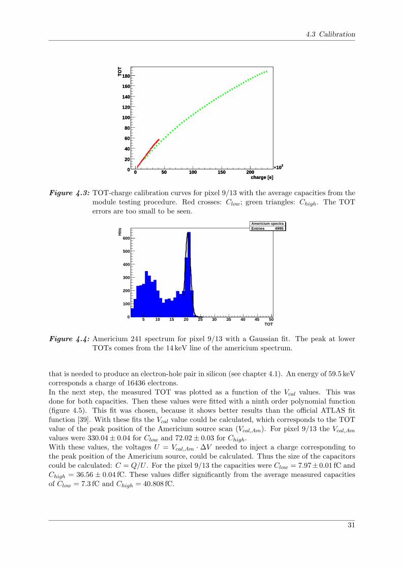
that is needed to produce an electron-hole pair in silicon (see chapter 4.1). An energy of 59.5 keVcorresponds a charge of 16436 electrons.In the next step, the measured TOT was plotted as a function of the Vcal values. This wasdone for both capacities. Then these values were fitted with a ninth order polynomial function(figure 4.5). This fit was chosen, because it shows better results than the official ATLAS fitfunction [39]. With these fits the Vcal value could be calculated, which corresponds to the TOTvalue of the peak position of the Americium source scan (Vcal,Am). For pixel 9/13 the Vcal,Am
values were 330.04± 0.04 for Clow and 72.02± 0.03 for Chigh.With these values, the voltages U = Vcal,Am · ∆V needed to inject a charge corresponding tothe peak position of the Americium source, could be calculated. Thus the size of the capacitorscould be calculated: C = Q/U . For the pixel 9/13 the capacities were Clow = 7.97±0.01 fC andChigh = 36.56 ± 0.04 fC. These values differ significantly from the average measured capacitiesof Clow = 7.3 fC and Chigh = 40.808 fC.
31
4 The Laser System
Vcal0 200 400 600 800 1000
TO
T
0
10
20
30
40
50
60
Vcal0 200 400 600 800 1000
TO
T
20
40
60
80
100
120
140
160
180
200
Figure 4.5: Measured TOT values for pixel 9/13 as a function of the Vcal values fitted with aninth order polynomial; left: Clow; right: Chigh. The TOT errors are too small tobe seen.
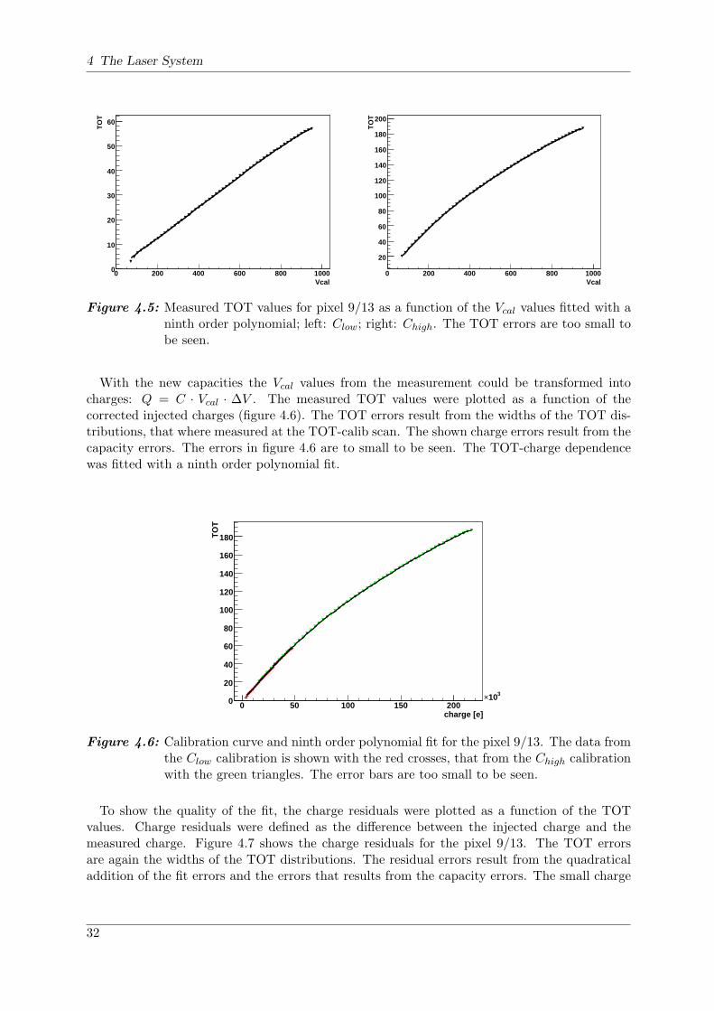
With the new capacities the Vcal values from the measurement could be transformed intocharges: Q = C · Vcal · ∆V . The measured TOT values were plotted as a function of thecorrected injected charges (figure 4.6). The TOT errors result from the widths of the TOT dis-tributions, that where measured at the TOT-calib scan. The shown charge errors result from thecapacity errors. The errors in figure 4.6 are to small to be seen. The TOT-charge dependencewas fitted with a ninth order polynomial fit.
charge [e]0 50 100 150 200
310×
TO
T
0
20
40
60
80
100
120
140
160
180
Figure 4.6: Calibration curve and ninth order polynomial fit for the pixel 9/13. The data fromthe Clow calibration is shown with the red crosses, that from the Chigh calibrationwith the green triangles. The error bars are too small to be seen.
To show the quality of the fit, the charge residuals were plotted as a function of the TOTvalues. Charge residuals were defined as the difference between the injected charge and themeasured charge. Figure 4.7 shows the charge residuals for the pixel 9/13. The TOT errorsare again the widths of the TOT distributions. The residual errors result from the quadraticaladdition of the fit errors and the errors that results from the capacity errors. The small charge
32
4.3 Calibration
residuals show that the applied polynomial fit yields good results for the charge calibration.Figure 4.7 still shows a little offset between the Clow and the Chigh calibration. Reasons for thisoffset can be a yet too imprecise calculation of the capacitances or the assumption that the ∆Vsteps have always the same range.
TOT0 20 40 60 80 100 120 140 160 180
char
ge r
esid
ual [
e]
−800
−600
−400
−200
0
200
400
600
800
TOT0 20 40 60 80 100 120 140 160 180
char
ge r
esid
ual [
e]
−800
−600
−400
−200
0
200
400
600
800
Figure 4.7: Charge residuals for pixel 9/13. The data from the Clow calibration is shown withthe red crosses, that from the Chigh calibration with the green triangles.
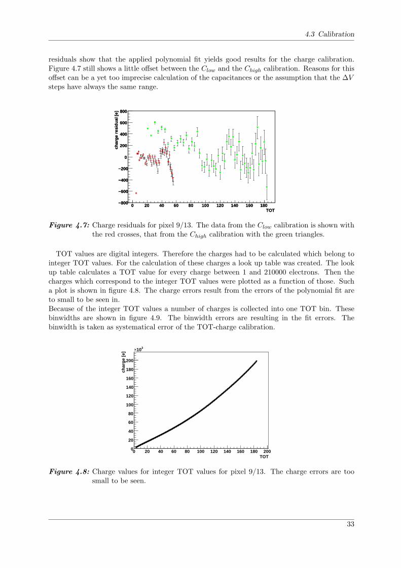
TOT values are digital integers. Therefore the charges had to be calculated which belong tointeger TOT values. For the calculation of these charges a look up table was created. The lookup table calculates a TOT value for every charge between 1 and 210000 electrons. Then thecharges which correspond to the integer TOT values were plotted as a function of those. Sucha plot is shown in figure 4.8. The charge errors result from the errors of the polynomial fit areto small to be seen in.Because of the integer TOT values a number of charges is collected into one TOT bin. Thesebinwidths are shown in figure 4.9. The binwidth errors are resulting in the fit errors. Thebinwidth is taken as systematical error of the TOT-charge calibration.
TOT0 20 40 60 80 100 120 140 160 180 200
char
ge [e
]
0
20
40
60
80
100
120
140
160
180
200
310×
Figure 4.8: Charge values for integer TOT values for pixel 9/13. The charge errors are toosmall to be seen.
33
4 The Laser System
TOT0 20 40 60 80 100 120 140 160 180 200
Bin
wid
th [e
]
800
1000
1200
1400
1600
1800
2000
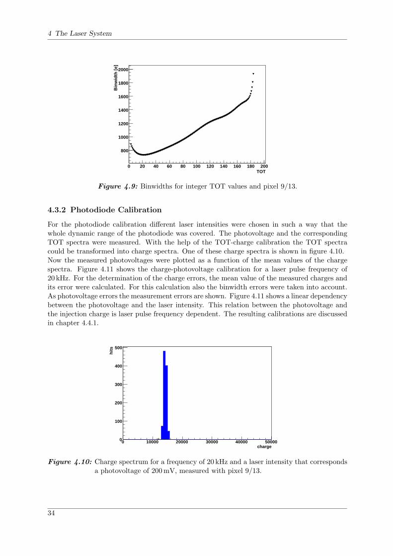
Figure 4.9: Binwidths for integer TOT values and pixel 9/13.
4.3.2 Photodiode Calibration
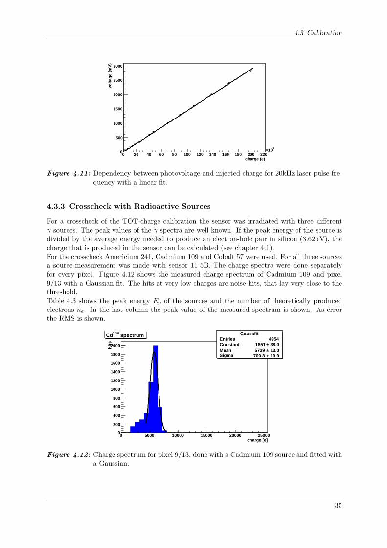
For the photodiode calibration different laser intensities were chosen in such a way that thewhole dynamic range of the photodiode was covered. The photovoltage and the correspondingTOT spectra were measured. With the help of the TOT-charge calibration the TOT spectracould be transformed into charge spectra. One of these charge spectra is shown in figure 4.10.Now the measured photovoltages were plotted as a function of the mean values of the chargespectra. Figure 4.11 shows the charge-photovoltage calibration for a laser pulse frequency of20 kHz. For the determination of the charge errors, the mean value of the measured charges andits error were calculated. For this calculation also the binwidth errors were taken into account.As photovoltage errors the measurement errors are shown. Figure 4.11 shows a linear dependencybetween the photovoltage and the laser intensity. This relation between the photovoltage andthe injection charge is laser pulse frequency dependent. The resulting calibrations are discussedin chapter 4.4.1.
Entries 999
Mean 1.39e+04
charge0 10000 20000 30000 40000 50000
hits
0
100
200
300
400
500
Entries 999
Mean 1.39e+04
Figure 4.10: Charge spectrum for a frequency of 20 kHz and a laser intensity that correspondsa photovoltage of 200mV, measured with pixel 9/13.
34
4.3 Calibration
charge (e)0 20 40 60 80 100 120 140 160 180 200 220
310×
volta
ge (
mV
)
0
500
1000
1500
2000
2500
3000
Figure 4.11: Dependency between photovoltage and injected charge for 20kHz laser pulse fre-quency with a linear fit.
4.3.3 Crosscheck with Radioactive Sources
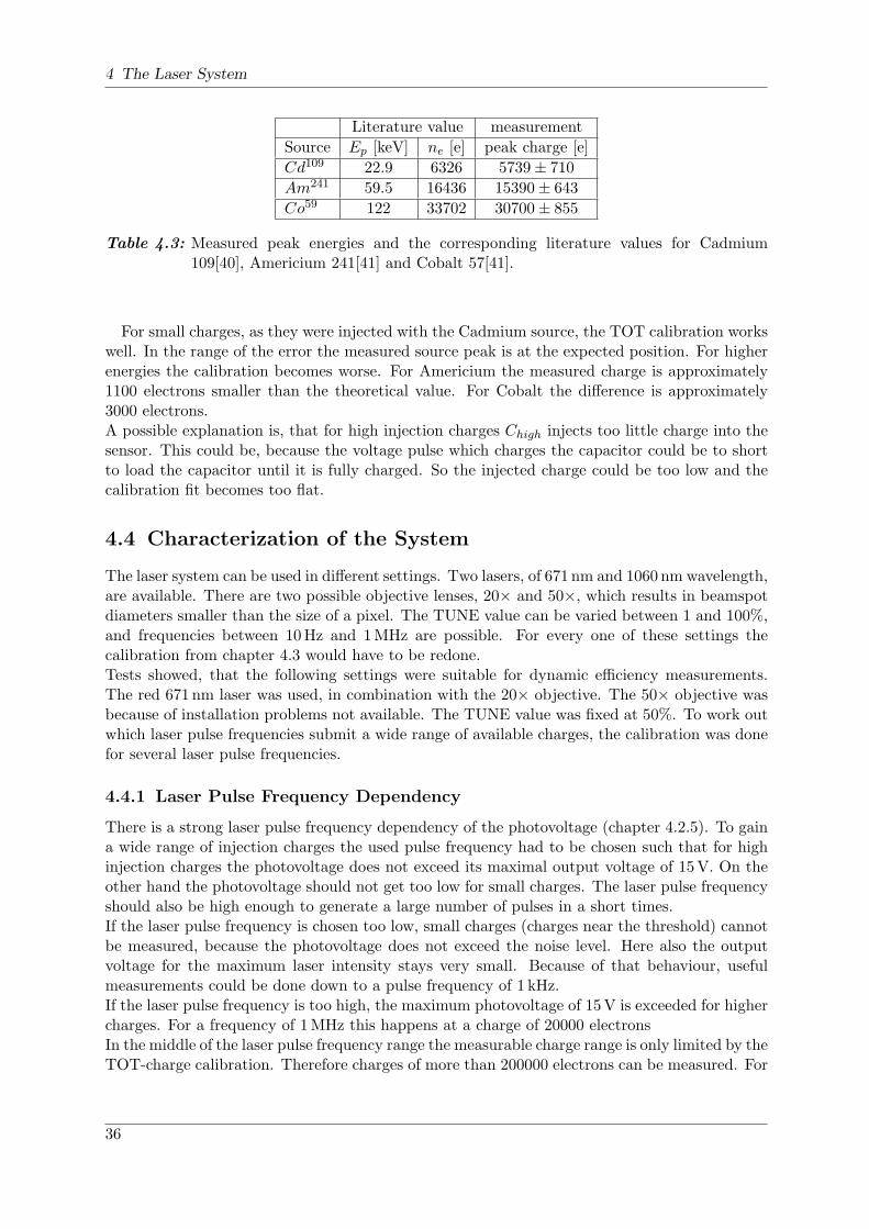
For a crosscheck of the TOT-charge calibration the sensor was irradiated with three differentγ-sources. The peak values of the γ-spectra are well known. If the peak energy of the source isdivided by the average energy needed to produce an electron-hole pair in silicon (3.62 eV), thecharge that is produced in the sensor can be calculated (see chapter 4.1).For the crosscheck Americium 241, Cadmium 109 and Cobalt 57 were used. For all three sourcesa source-measurement was made with sensor 11-5B. The charge spectra were done separatelyfor every pixel. Figure 4.12 shows the measured charge spectrum of Cadmium 109 and pixel9/13 with a Gaussian fit. The hits at very low charges are noise hits, that lay very close to thethreshold.Table 4.3 shows the peak energy Ep of the sources and the number of theoretically producedelectrons ne. In the last column the peak value of the measured spectrum is shown. As errorthe RMS is shown.
GaussfitEntries 4954Constant 38.0± 1851 Mean 13.0± 5739 Sigma 10.0± 709.8
charge [e]0 5000 10000 15000 20000 25000
hits
0
200
400
600
800
1000
1200
1400
1600
1800
2000
GaussfitEntries 4954Constant 38.0± 1851 Mean 13.0± 5739 Sigma 10.0± 709.8
spectrum109Cd
Figure 4.12: Charge spectrum for pixel 9/13, done with a Cadmium 109 source and fitted witha Gaussian.
35
4 The Laser System
Literature value measurement
Source Ep [keV] ne [e] peak charge [e]
Cd109 22.9 6326 5739± 710
Am241 59.5 16436 15390± 643
Co59 122 33702 30700± 855
Table 4.3: Measured peak energies and the corresponding literature values for Cadmium109[40], Americium 241[41] and Cobalt 57[41].
For small charges, as they were injected with the Cadmium source, the TOT calibration workswell. In the range of the error the measured source peak is at the expected position. For higherenergies the calibration becomes worse. For Americium the measured charge is approximately1100 electrons smaller than the theoretical value. For Cobalt the difference is approximately3000 electrons.A possible explanation is, that for high injection charges Chigh injects too little charge into thesensor. This could be, because the voltage pulse which charges the capacitor could be to shortto load the capacitor until it is fully charged. So the injected charge could be too low and thecalibration fit becomes too flat.
4.4 Characterization of the System
The laser system can be used in different settings. Two lasers, of 671 nm and 1060 nm wavelength,are available. There are two possible objective lenses, 20× and 50×, which results in beamspotdiameters smaller than the size of a pixel. The TUNE value can be varied between 1 and 100%,and frequencies between 10Hz and 1MHz are possible. For every one of these settings thecalibration from chapter 4.3 would have to be redone.Tests showed, that the following settings were suitable for dynamic efficiency measurements.The red 671 nm laser was used, in combination with the 20× objective. The 50× objective wasbecause of installation problems not available. The TUNE value was fixed at 50%. To work outwhich laser pulse frequencies submit a wide range of available charges, the calibration was donefor several laser pulse frequencies.
4.4.1 Laser Pulse Frequency Dependency
There is a strong laser pulse frequency dependency of the photovoltage (chapter 4.2.5). To gaina wide range of injection charges the used pulse frequency had to be chosen such that for highinjection charges the photovoltage does not exceed its maximal output voltage of 15V. On theother hand the photovoltage should not get too low for small charges. The laser pulse frequencyshould also be high enough to generate a large number of pulses in a short times.If the laser pulse frequency is chosen too low, small charges (charges near the threshold) cannotbe measured, because the photovoltage does not exceed the noise level. Here also the outputvoltage for the maximum laser intensity stays very small. Because of that behaviour, usefulmeasurements could be done down to a pulse frequency of 1 kHz.If the laser pulse frequency is too high, the maximum photovoltage of 15V is exceeded for highercharges. For a frequency of 1MHz this happens at a charge of 20000 electronsIn the middle of the laser pulse frequency range the measurable charge range is only limited by theTOT-charge calibration. Therefore charges of more than 200000 electrons can be measured. For
36
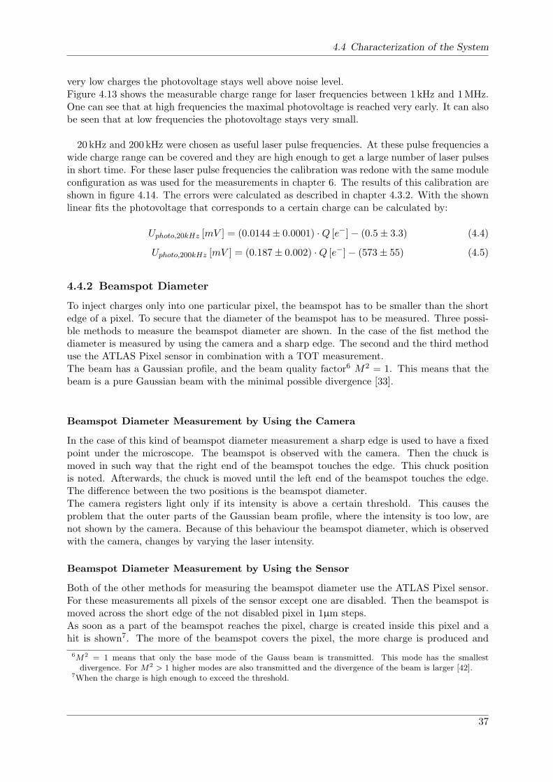
4.4 Characterization of the System
very low charges the photovoltage stays well above noise level.Figure 4.13 shows the measurable charge range for laser frequencies between 1 kHz and 1MHz.One can see that at high frequencies the maximal photovoltage is reached very early. It can alsobe seen that at low frequencies the photovoltage stays very small.
20 kHz and 200 kHz were chosen as useful laser pulse frequencies. At these pulse frequencies awide charge range can be covered and they are high enough to get a large number of laser pulsesin short time. For these laser pulse frequencies the calibration was redone with the same moduleconfiguration as was used for the measurements in chapter 6. The results of this calibration areshown in figure 4.14. The errors were calculated as described in chapter 4.3.2. With the shownlinear fits the photovoltage that corresponds to a certain charge can be calculated by:
Uphoto,20kHz [mV ] = (0.0144± 0.0001) ·Q [e−]− (0.5± 3.3) (4.4)
Uphoto,200kHz [mV ] = (0.187± 0.002) ·Q [e−]− (573± 55) (4.5)
4.4.2 Beamspot Diameter
To inject charges only into one particular pixel, the beamspot has to be smaller than the shortedge of a pixel. To secure that the diameter of the beamspot has to be measured. Three possi-ble methods to measure the beamspot diameter are shown. In the case of the fist method thediameter is measured by using the camera and a sharp edge. The second and the third methoduse the ATLAS Pixel sensor in combination with a TOT measurement.The beam has a Gaussian profile, and the beam quality factor6 M2 = 1. This means that thebeam is a pure Gaussian beam with the minimal possible divergence [33].
Beamspot Diameter Measurement by Using the Camera
In the case of this kind of beamspot diameter measurement a sharp edge is used to have a fixedpoint under the microscope. The beamspot is observed with the camera. Then the chuck ismoved in such way that the right end of the beamspot touches the edge. This chuck positionis noted. Afterwards, the chuck is moved until the left end of the beamspot touches the edge.The difference between the two positions is the beamspot diameter.The camera registers light only if its intensity is above a certain threshold. This causes theproblem that the outer parts of the Gaussian beam profile, where the intensity is too low, arenot shown by the camera. Because of this behaviour the beamspot diameter, which is observedwith the camera, changes by varying the laser intensity.
Beamspot Diameter Measurement by Using the Sensor
Both of the other methods for measuring the beamspot diameter use the ATLAS Pixel sensor.For these measurements all pixels of the sensor except one are disabled. Then the beamspot ismoved across the short edge of the not disabled pixel in 1µm steps.As soon as a part of the beamspot reaches the pixel, charge is created inside this pixel and ahit is shown7. The more of the beamspot covers the pixel, the more charge is produced and
6M2 = 1 means that only the base mode of the Gauss beam is transmitted. This mode has the smallestdivergence. For M2 > 1 higher modes are also transmitted and the divergence of the beam is larger [42].
7When the charge is high enough to exceed the threshold.
37
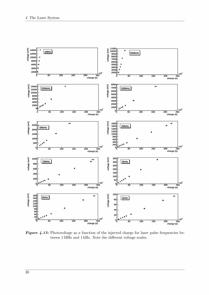
4 The Laser System
charge (e)0 50 100 150 200 250
310×
volta
ge (
mV
)
2000
4000
6000
8000
10000
12000
140001MHz
charge (e)0 50 100 150 200 250
310×
volta
ge (
mV
)
20003000400050006000700080009000
1000011000
500kHz
charge (e)0 50 100 150 200 250
310×
volta
ge (
mV
)
02000400060008000
100001200014000
200kHz
charge (e)0 50 100 150 200 250
310×vo
ltage
(m
V)
0
100020003000
400050006000
70008000
100kHz
charge (e)0 50 100 150 200 250
310×
volta
ge (
mV
)
0
500
1000
1500
2000
250050kHz
charge (e)0 50 100 150 200 250
310×
volta
ge (
mV
)
0200400600800
10001200140016001800
20kHz
charge (e)0 50 100 150 200 250
310×
volta
ge (
mV
)
0
200
400
600
800
100010kHz
charge (e)0 50 100 150 200 250
310×
volta
ge (
mV
)
0
50
100
150
200
250
300
350
5kHz
charge (e)0 50 100 150 200 250
310×
volta
ge (
mV
)
020406080
100120140160180
2kHz
charge (e)0 50 100 150 200 250
310×
volta
ge (
mV
)
0
20
40
60
80
100
1kHz
Figure 4.13: Photovoltage as a function of the injected charge for laser pulse frequencies be-tween 1MHz and 1 kHz. Note the different voltage scales.
38
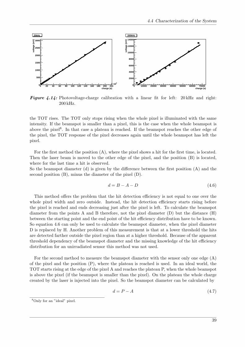
4.4 Characterization of the System
charge (e)0 20 40 60 80 100 120 140 160 180 200 220
310×
volta
ge (
mV
)
0
500
1000
1500
2000
2500
3000
20kHz
charge (e)0 10000 20000 30000 40000 50000 60000 70000
volta
ge (
mV
)
0
2000
4000
6000
8000
10000
12000
14000
200kHz
Figure 4.14: Photovoltage-charge calibration with a linear fit for left: 20 kHz and right:200 kHz.
the TOT rises. The TOT only stops rising when the whole pixel is illuminated with the sameintensity. If the beamspot is smaller than a pixel, this is the case when the whole beamspot isabove the pixel8. In that case a plateau is reached. If the beamspot reaches the other edge ofthe pixel, the TOT response of the pixel decreases again until the whole beamspot has left thepixel.
For the first method the position (A), where the pixel shows a hit for the first time, is located.Then the laser beam is moved to the other edge of the pixel, and the position (B) is located,where for the last time a hit is observed.So the beamspot diameter (d) is given by the difference between the first position (A) and thesecond position (B), minus the diameter of the pixel (D).
d = B −A−D (4.6)
This method offers the problem that the hit detection efficiency is not equal to one over thewhole pixel width and zero outside. Instead, the hit detection efficiency starts rising beforethe pixel is reached and ends decreasing just after the pixel is left. To calculate the beamspotdiameter from the points A and B therefore, not the pixel diameter (D) but the distance (H)between the starting point and the end point of the hit efficiency distribution have to be known.So equation 4.6 can only be used to calculate the beamspot diameter, when the pixel diameterD is replaced by H. Another problem of this measurement is that at a lower threshold the hitsare detected farther outside the pixel region than at a higher threshold. Because of the apparentthreshold dependency of the beamspot diameter and the missing knowledge of the hit efficiencydistribution for an unirradiated sensor this method was not used.
For the second method to measure the beamspot diameter with the sensor only one edge (A)of the pixel and the position (P), where the plateau is reached is used. In an ideal world, theTOT starts rising at the edge of the pixel A and reaches the plateau P, when the whole beamspotis above the pixel (if the beamspot is smaller than the pixel). On the plateau the whole chargecreated by the laser is injected into the pixel. So the beamspot diameter can be calculated by
d = P −A (4.7)
8Only for an ”ideal” pixel.
39
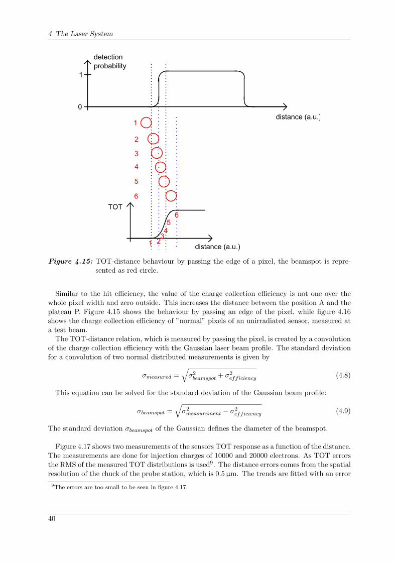
4 The Laser System
detection
probability
1
0
distance (a.u.)1
2
3
4
5
6
1 23
6
45
TOT
distance (a.u.)
Figure 4.15: TOT-distance behaviour by passing the edge of a pixel, the beamspot is repre-sented as red circle.
Similar to the hit efficiency, the value of the charge collection efficiency is not one over thewhole pixel width and zero outside. This increases the distance between the position A and theplateau P. Figure 4.15 shows the behaviour by passing an edge of the pixel, while figure 4.16shows the charge collection efficiency of ”normal” pixels of an unirradiated sensor, measured ata test beam.The TOT-distance relation, which is measured by passing the pixel, is created by a convolution
of the charge collection efficiency with the Gaussian laser beam profile. The standard deviationfor a convolution of two normal distributed measurements is given by
σmeasured =√
σ2beamspot + σ2
efficiency (4.8)
This equation can be solved for the standard deviation of the Gaussian beam profile:
σbeamspot =√
σ2measurement − σ2
efficiency (4.9)
The standard deviation σbeamspot of the Gaussian defines the diameter of the beamspot.
Figure 4.17 shows two measurements of the sensors TOT response as a function of the distance.The measurements are done for injection charges of 10000 and 20000 electrons. As TOT errorsthe RMS of the measured TOT distributions is used9. The distance errors comes from the spatialresolution of the chuck of the probe station, which is 0.5µm. The trends are fitted with an error
9The errors are too small to be seen in figure 4.17.
40
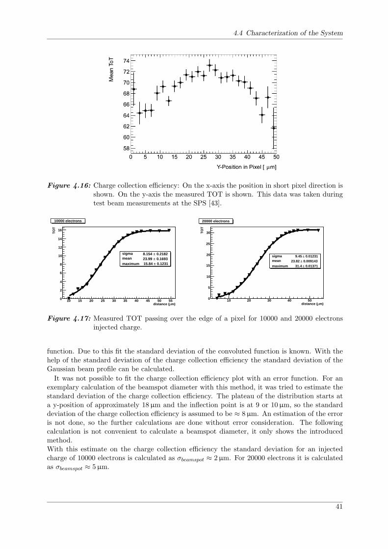
4.4 Characterization of the System
Figure 4.16: Charge collection efficiency: On the x-axis the position in short pixel direction isshown. On the y-axis the measured TOT is shown. This data was taken duringtest beam measurements at the SPS [43].
m)µdistance (10 15 20 25 30 35 40 45 50 55
TO
T
0
2
4
6
8
10
12
14
16
sigma 0.2182± 8.154 mean 0.1693± 23.99 maximum 0.1231± 15.84
sigma 0.2182± 8.154 mean 0.1693± 23.99 maximum 0.1231± 15.84
10000 electrons
m)µdistance (10 20 30 40 50
TO
T
0
5
10
15
20
25
30
sigma 0.01231± 9.45 mean 0.009143± 23.82 maximum 0.01371± 31.4
sigma 0.01231± 9.45 mean 0.009143± 23.82 maximum 0.01371± 31.4
20000 electrons
Figure 4.17: Measured TOT passing over the edge of a pixel for 10000 and 20000 electronsinjected charge.
function. Due to this fit the standard deviation of the convoluted function is known. With thehelp of the standard deviation of the charge collection efficiency the standard deviation of theGaussian beam profile can be calculated.
It was not possible to fit the charge collection efficiency plot with an error function. For anexemplary calculation of the beamspot diameter with this method, it was tried to estimate thestandard deviation of the charge collection efficiency. The plateau of the distribution starts ata y-position of approximately 18µm and the inflection point is at 9 or 10µm, so the standarddeviation of the charge collection efficiency is assumed to be ≈ 8µm. An estimation of the erroris not done, so the further calculations are done without error consideration. The followingcalculation is not convenient to calculate a beamspot diameter, it only shows the introducedmethod.With this estimate on the charge collection efficiency the standard deviation for an injectedcharge of 10000 electrons is calculated as σbeamspot ≈ 2µm. For 20000 electrons it is calculatedas σbeamspot ≈ 5µm.
41
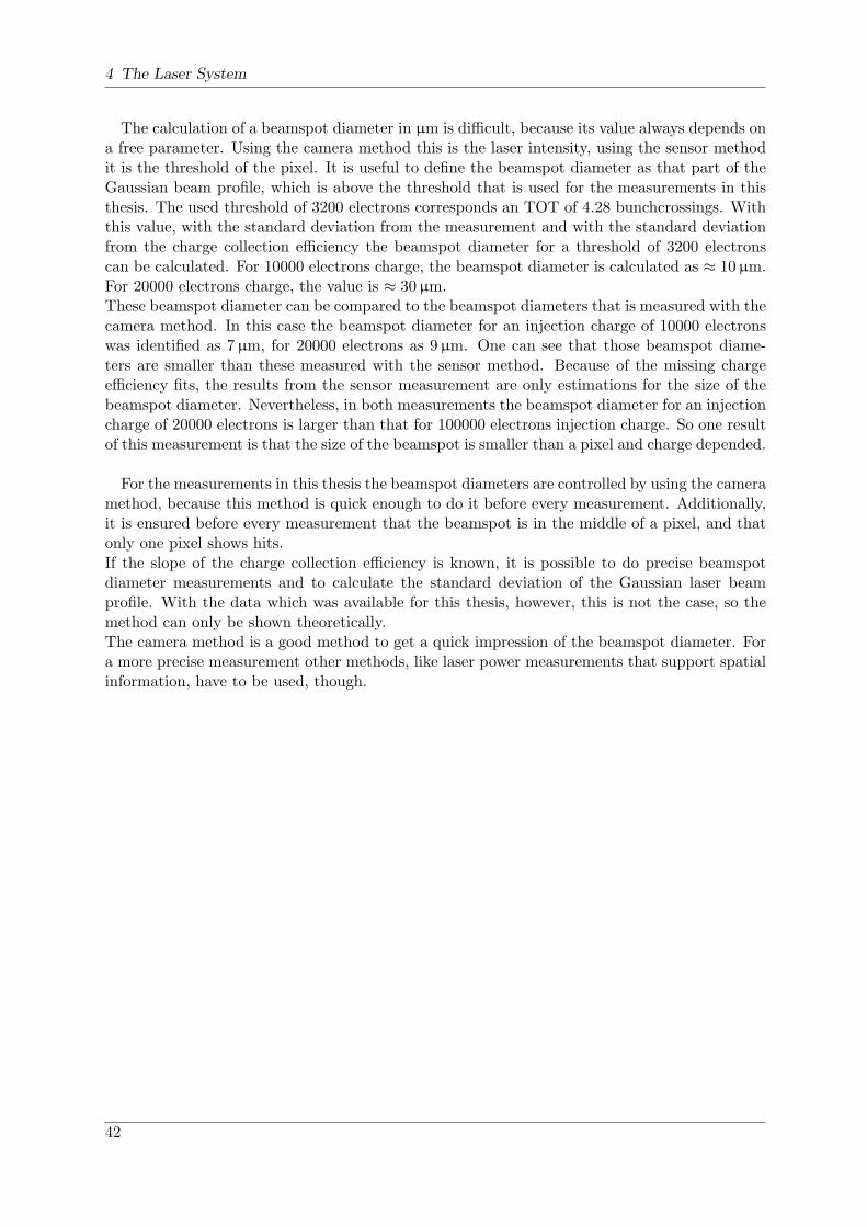
4 The Laser System
The calculation of a beamspot diameter in µm is difficult, because its value always depends ona free parameter. Using the camera method this is the laser intensity, using the sensor methodit is the threshold of the pixel. It is useful to define the beamspot diameter as that part of theGaussian beam profile, which is above the threshold that is used for the measurements in thisthesis. The used threshold of 3200 electrons corresponds an TOT of 4.28 bunchcrossings. Withthis value, with the standard deviation from the measurement and with the standard deviationfrom the charge collection efficiency the beamspot diameter for a threshold of 3200 electronscan be calculated. For 10000 electrons charge, the beamspot diameter is calculated as ≈ 10µm.For 20000 electrons charge, the value is ≈ 30µm.These beamspot diameter can be compared to the beamspot diameters that is measured with thecamera method. In this case the beamspot diameter for an injection charge of 10000 electronswas identified as 7µm, for 20000 electrons as 9µm. One can see that those beamspot diame-ters are smaller than these measured with the sensor method. Because of the missing chargeefficiency fits, the results from the sensor measurement are only estimations for the size of thebeamspot diameter. Nevertheless, in both measurements the beamspot diameter for an injectioncharge of 20000 electrons is larger than that for 100000 electrons injection charge. So one resultof this measurement is that the size of the beamspot is smaller than a pixel and charge depended.
For the measurements in this thesis the beamspot diameters are controlled by using the cameramethod, because this method is quick enough to do it before every measurement. Additionally,it is ensured before every measurement that the beamspot is in the middle of a pixel, and thatonly one pixel shows hits.If the slope of the charge collection efficiency is known, it is possible to do precise beamspotdiameter measurements and to calculate the standard deviation of the Gaussian laser beamprofile. With the data which was available for this thesis, however, this is not the case, so themethod can only be shown theoretically.The camera method is a good method to get a quick impression of the beamspot diameter. Fora more precise measurement other methods, like laser power measurements that support spatialinformation, have to be used, though.
42
5 Sample Characterisation
The measurements in this thesis were done with two different silicon sensors. The first one wasunirradiated and its reactions were known very well. The second sensor was irradiated withthermal neutrons up to a dose of 1 · 1015cm−2 neutron equivalent. That conforms the ATLASlifetime dose.For both samples the same tuning and characterization procedure was used. The samples weretuned to a threshold of 3200 electrons and the TOT was tuned such that 20000 electrons corre-sponded a TOT of 30. The whole procedure consists of the following steps:
• Digital test
• Analog test
• Threshold tuning
• TOT tuning
• Monleak scan
• IV scan
The individual steps are described in the following chapter.
5.1 Sample 11-5B
The sample 11-5B was used to compare its behaviours with the irradiated sample. It was tunedand characterized in the same way as the irradiated sample. This way the changes between anunirradiated and an irradiated sample can be shown.All tests and measurements with this sample were done at a bias voltage of -150V and at roomtemperature. The leakage current was approximately 0.2µA. To verify the function of thedigital part of the FE-chip, a digital test was done. At this measurement a charge was injected200 times into the digital read out electronics of the FE-chip. The chip showed a very consistentresponse. All pixels of the chip registered the 200 injected charges. Also the analogue test,which injects a charge 200 times into the analogue part of the FE-chip, showed a completelyuniform response of the electronics. Every pixel showed the 200 charges which were injected.The threshold was tuned by using the global and the individual threshold DAC’s. The thresh-
old scan, which was done at the end of the tuning procedure showed a threshold of 3199 electronswith a RMS of 27 electrons. The noise of the s-curve (see chapter 3.1.2) was σ = 176.8 ± 10.8electrons. The results of the threshold scan are shown in figure 5.1. With the IF-DAC and F-DAC tuning the TOT for a injected charge of 20000 electrons was tuned to 33.52 bunchcrossingswith a RMS of 2.84.To receive information about the uniformity of the leakage current a monleak scan was done.This scan measures the combined feedback and leakage current from the feedback circuit
Imonleak = Ileak + 2 · If (5.1)
43

5 Sample Characterisation
Column0 2 4 6 8 10 12 14 16
Row
020406080
100120140
2500
3000
3500
4000
4500
Constant 770.3Mean 3199Sigma 27.13
2500 3000 3500 4000 4500
100200300400500600700
Constant 770.3Mean 3199Sigma 27.13
"Channel" = row+160*column+2880*chip0 500 1000 1500 2000 2500
2500
3000
3500
4000
4500
Column0 2 4 6 8 10 12 14 16
Row
020406080
100120140
150
200
250
300
350
400
Constant 304.3Mean 176.8Sigma 10.77
150 200 250 300 350 400
50100150200250300350400
Constant 304.3Mean 176.8Sigma 10.77
"Channel" = row+160*column+2880*chip0 500 1000 1500 2000 2500
150200250300350400
Figure 5.1: Left: Threshold-curve, right: Noise. Top: pixelmap with threshold and noiseinformation. Middle: threshold and noise distribution. Bottom: threshold andnoise for each of the 2880 pixels.
IV (V)-300 -250 -200 -150 -100 -50 0
IV -
cur
rent
(A
)
-0.22
-0.2
-0.18
-0.16
-0.14
-0.12
-0.1
-0.08
-0.06
-0.04
-610×
Figure 5.2: IV curve: Dependence of the leakage current on the bias voltage.
44
5.2 Sample 4-6B
where If is defined by the IF and F-DAC parameters [9]. The monleak scan showed a homo-geneous behaviour for the whole chip. There was no evidence for pixels with increased leakagecurrents.The last scan that was done was an IV-scan. Here the bias voltage was changed in steps from-10V to -300V and the corresponding leakage current was measured. Figure 5.2 shows the IV-curve for sample 11-5B. At smaller bias voltages the leakage current is rising sharply, at higherbias voltages the dependency becomes more linear. Up to a bias voltage of -300V, the IV-curvedoes not show a breakdown.
5.2 Sample 4-6B
This sample was irradiated with thermal neutrons to a dose of 1 · 1015cm2 neutron equivalent.This is the ATLAS lifetime dose for a pixel module. With this the behaviour of the sensor andthe FE-chip at the end of the ALTAS lifetime can be studied.To minimize the leakage current, the tuning procedure and the later measurements were doneat a chuck temperature of -40C. That corresponds a sensor temperature1 of approximately-25C. The sensor was in a good state and the tuning of the chip was possible without biggerproblems. The tuning and characterization procedure was done at a bias voltage of -600V.This is the maximal possible voltage in the ATLAS detector. At -600V the leakage currentwas approximately 2.2µA. Because of sensor and electronics defects which were generated byirradiation, the sample showed more noise than the unirradiated sample. In the analogue testthe most normal pixels showed 200 injected hits, but especially the long ganged and intergangedpixels were noisy. They showed up to 220 hits. The long pixels showed more noise, becausethey have a bigger surface then the normal pixels, and they lay at the edges of the sensor.Leakage current from the edge of the sensor increases the noise for these pixels. The reason forthe higher noise level of the ganged pixels is the fact, that in comparison to normal pixels, thesensor surface is doubled. The digital test showed no differences to the unirradiated sample,where all pixels showed the 200 injected charges.
It was not possible to do a normal G-DAC tuning. The tuning procedure choose theG-DAC value very low. That increases the noise heavily and made a threshold scan impos-sible. This problem was fixed by setting the G-DAC value by hand to a higher value of 24. Withthis setting the noise was decreased and the T-DAC tune and threshold scan worked. Figure 5.3shows the threshold distribution for sample 4-6B. With 3261 ± 49 electrons the threshold wasfurther away from the set value of 3200 electrons than at sample 11-5B. With σ = 290.3± 17.8electrons also the noise was approximately 100 electrons higher than at sample 11-5B. The noisedistribution (figure 5.3 middle, right) shows a smaller peak at high values. One reason for thispeak are the long ganged and intergang pixels. Especially the long pixels show a different be-haviour, as can be seen in the hitmap and the pixelnumber-threshold plot (figure 5.3 upmost andbottommost). However it can be seen that also many normal pixels are responsible for the peak.The reason for this behaviour lies in the worse performance of these pixels after irradiation. Infigure 5.3 (top) it also can be seen that there are pixels, where the fit does not work (shown inwhite). Especially the long pixels and a few ganged pixels were too noisy to be fitted. The TOTfor 20000 electrons was tuned to 33.53 bunchcrossings, with a RMS of 2.84. Here the tuningitself worked without any differences to sample 11-5B, also the tuned value was very similar.Only the RMS was a bit higher as at sample 11-5B.
1Measured with the NTC of the single chip card attachment.
45
5 Sample Characterisation
Constant 784Mean 3261Sigma 48.73
2500 3000 3500 4000 4500 5000 5500 6000 6500
100
200
300
400
500
600
700
800
Constant 784Mean 3261Sigma 48.73
Column0 2 4 6 8 10 12 14 16
Row
0
20
40
60
80
100
120
140
2500
3000
3500
4000
4500
5000
5500
6000
6500
"Channel" = row+160*column+2880*chip0 500 1000 1500 2000 2500
2500
3000
3500
40004500
5000
5500
60006500
Column0 2 4 6 8 10 12 14 16
Row
0
20
40
60
80
100
120
140
200
250
300
350
400
450
500
550
"Channel" = row+160*column+2880*chip0 500 1000 1500 2000 2500
200
250
300
350
400
450
500
550
Constant 182.6Mean 290.3Sigma 17.83
200 250 300 350 400 450 500 550
20406080
100120140160180200
Constant 182.6Mean 290.3Sigma 17.83
Figure 5.3: Left: Threshold-curve, right: Noise. Top: pixelmap with the threshold and noiseinformation, with pixels where the s-curve fit did not converge (in white). Middle:threshold and noise distribution. Bottom: threshold and noise for each of the 2880pixels.
IV (V)-1000 -800 -600 -400 -200 0
IV -
cur
rent
(A
)
-3
-2.5
-2
-1.5
-1
-0.5
-610×
Figure 5.4: IV-curve: Dependence of the leakage current on the bias voltage.
46
5.2 Sample 4-6B
A monleak scan was done, which showed higher monleak currents and a bigger spread of thedistribution than the unirradiated sample. This was expected because of the higher leakagecurrent of the whole sensor. Apart from that there was nothing special in the monleak scan.The monleak current was uniform for the whole sensor.An IV-scan was done up to a bias voltage of -1000V. In figure 5.4 the scan results are shown.On the measured bias voltage range no breakdown can be seen.
Table 5.1 shows the parameters of the evaluated samples. With the limitation that the G-DAC value had to be set by hand, the irradiated sample could be tuned and used in the sameway as the unirradiated sample. The noise level and the leakage current of the irradiated samplewere higher than at the non irradiated one. Especially the long pixels were very noisy and manyof them could not be tuned. After irradiation with the ATLAS lifetime dose the sample 4-6Bshowed a good performance and it was still usable for particle detection.
11-5B 4-6B
Dose [Neq] 0 1 · 1015Irradiation type - thermal neutrons
Chuck temperature room temperature -40C
Temperature near the sensor room temperature -24C
Vbias [V] -150 -600
Il [µA] 0.2 2.1
Threshold [e−] 3199± 27 3261± 49
Width of the threshold distribution [e−] 176.8± 10.8 290.3± 17.8
TOT20000 33± 2 33± 3
Table 5.1: Characteristics of the studied samples.
47

6 Time-Resolved Hit Efficency
Measurements
Every 25 ns a LHC bunchcrossing happens inside the ATLAS detector. The FE-chip has to relatethe collected hits to the correct bunchcrossings. The detection probability during a bunchcross-ing is studied before and after the irradiation of a module. The unirradiated sample 11-5B andthe irradiated sample 4-6B are used. An ideal module would have a detection probability ofone during the correct bunchcrossing and zero before and afterwards (figure 6.1 left). In caseof the real module the detection probability rises at the beginning of the bunchcrossing up to avalue near one and decreases to zero again at the end of the bunchcrossing (figure 6.1 right). Inthis chapter the behaviour of the detection probability will be studied for an unirradiated andan irradiated sample. The detection probability in the middle of the bunchcrossing, where theplateau of the distribution is reached and, the slopes of the distribution are evaluated.
25 ns 25 ns
tt
1 1
de
tection
pro
bab
ility
de
tection
pro
bab
ility
Figure 6.1: Detection probability for an ideal module (left) and for a real module (right).
To study these behaviours, laser pulses are injected into the sensor at different times duringthe bunchcrossig. For this, the laser pulses are delayed with respect to the clock. At the slopesof the detection probability distribution the laser is delayed in 1 ns steps. In the middle of thebunchcrossing, when the plateau is reached, the laser delay is changed in 2.5 ns steps. For everydelay time 1000 laser pulses are injected into the sensor and the number of hits that are detectedin the different LV1IDs is counted.For the evaluation, the data is fitted. The fit is a combination of a box fit and two error functionson the edges of the distribution. For the measurement of the slopes, the standard deviation fromthe error functions are used. The FWHM1 of the distribution and the point in time of the centerof the distribution are also given by the fit. The fit function is:
f(x) =1
2· (1 + F · (x− x0)) ·A ·
(
0.5 ·(
1 + erf(
x+W−x0√2·σ
)))
−(
0.5 ·(
1 + erf(
x−W−x0√2·σ
)))
W(6.1)
A, F, W, x0, and σ are parameters of the fit. W is the FWHM of the distribution dividedby two, and σ is the standard deviation of the error function. x0 gives the point in time of thecenter of the distribution. An example for recorded data with the fit is shown in figure 6.22.
1Full width half minimum; width of the distribution at a probability of 50%2In this plot, as in all other plots in this chapter, the error bars are not shown.
49
6 Time-Resolved Hit Efficency Measurements
delay(ns)0 10 20 30 40 50
dete
ctio
n pr
obab
ility
(%)
0
20
40
60
80
100
σ 0.04236± 1.787
A 9.107± 2442 0x 0.03487± 23.53
W 0.02967± 12.43
F 0.0006246± −0.000697
σ 0.04236± 1.787
A 9.107± 2442 0x 0.03487± 23.53
W 0.02967± 12.43
F 0.0006246± −0.000697
Figure 6.2: Example for a detection probability distribution fitted with equation 6.1.
The detection probability distribution is measured in three different ways. The time of thelaser injection can be varied by changing the time of the laser pulse emission. It is also possibleto change the arriving time of the trigger at the module. The third way is to change both,the laser pulse emission and the trigger arrival at the module together. As reference time forthe delay measurements, the first clock cycle that lies in the LV1ID window is defined as zero(measured without any delay). All delays are referred to this point in time. The phase betweenthe beginning of the bunchcrossing and the time of the laser injection is not known, but constantwithout delay.All measurements are done with two different injection charges. By traversing the sensor, a MIPcreates approximately 20000 electrons, so this charge is also chosen for the measurements. Thesecond charge that is used is 10000 electrons. It is chosen to see the behaviour at lower chargeslike they are produced after the irradiation of a sensor.For the detection probability measurements the beamspot diameter is set up small enough thatonly one pixel is illuminated by the laser. The diameter of the beamspot is controlled likedescribed in chapter 4.4.2. The laser beamspot is located in the middle of the used pixel. Allother pixels that are not illuminated are disabled to minimize noise hits.
6.1 The External Trigger
To study the detection probability during a bunchcrossing, hits are injected at different timesduring the bunchcrossing. For that task an external trigger system was installed (see figure 6.3),it is used to trigger the laser pulse emission and the read out trigger of the USBPix system.To generate the trigger signal a frequency generator AGF 3521 from Tektronix is used. Thisfrequency generator is triggered by the 40MHz clock from the single chip card. This way the out-put signal from the frequency generator is generated always at the rising edge of the clock fromthe single chip card. The output of the frequency generator shows a jitter of up to 100 ps [44].As trigger signal a 1µs long pulse is used. This pulse has a low level of 0V and a high level of5V, the rising time of the signal is 2.5 ns . It is send with a frequency of 20 kHz, which was oneof the frequencies that were calibrated in chapter 4.3.The output of the frequency generator is connected with LEMO cables of the same length tothe laser trigger input and to the external trigger input of the USBPix system. When thetrigger reaches the USBPix system, it read out a 16 bunchcrossings long LV1ID window (see
50
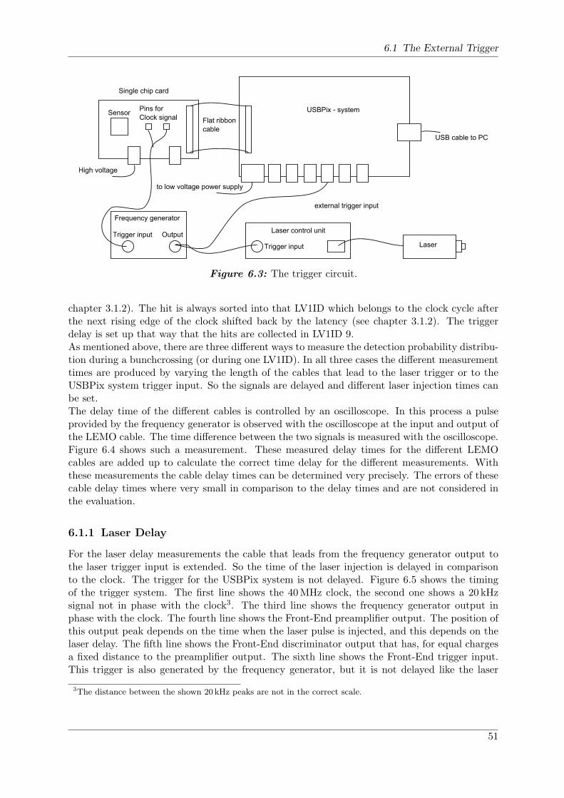
6.1 The External Trigger
USBPix - system
Single chip card
Sensor
USB cable to PC
to low voltage power supply
external trigger input
High voltage
Pins for
Clock signal
Frequency generator
Trigger input OutputLaser control unit
Trigger input Laser
Flat ribbon
cable
Figure 6.3: The trigger circuit.
chapter 3.1.2). The hit is always sorted into that LV1ID which belongs to the clock cycle afterthe next rising edge of the clock shifted back by the latency (see chapter 3.1.2). The triggerdelay is set up that way that the hits are collected in LV1ID 9.As mentioned above, there are three different ways to measure the detection probability distribu-tion during a bunchcrossing (or during one LV1ID). In all three cases the different measurementtimes are produced by varying the length of the cables that lead to the laser trigger or to theUSBPix system trigger input. So the signals are delayed and different laser injection times canbe set.The delay time of the different cables is controlled by an oscilloscope. In this process a pulseprovided by the frequency generator is observed with the oscilloscope at the input and output ofthe LEMO cable. The time difference between the two signals is measured with the oscilloscope.Figure 6.4 shows such a measurement. These measured delay times for the different LEMOcables are added up to calculate the correct time delay for the different measurements. Withthese measurements the cable delay times can be determined very precisely. The errors of thesecable delay times where very small in comparison to the delay times and are not considered inthe evaluation.
6.1.1 Laser Delay
For the laser delay measurements the cable that leads from the frequency generator output tothe laser trigger input is extended. So the time of the laser injection is delayed in comparisonto the clock. The trigger for the USBPix system is not delayed. Figure 6.5 shows the timingof the trigger system. The first line shows the 40MHz clock, the second one shows a 20 kHzsignal not in phase with the clock3. The third line shows the frequency generator output inphase with the clock. The fourth line shows the Front-End preamplifier output. The position ofthis output peak depends on the time when the laser pulse is injected, and this depends on thelaser delay. The fifth line shows the Front-End discriminator output that has, for equal chargesa fixed distance to the preamplifier output. The sixth line shows the Front-End trigger input.This trigger is also generated by the frequency generator, but it is not delayed like the laser
3The distance between the shown 20 kHz peaks are not in the correct scale.
51
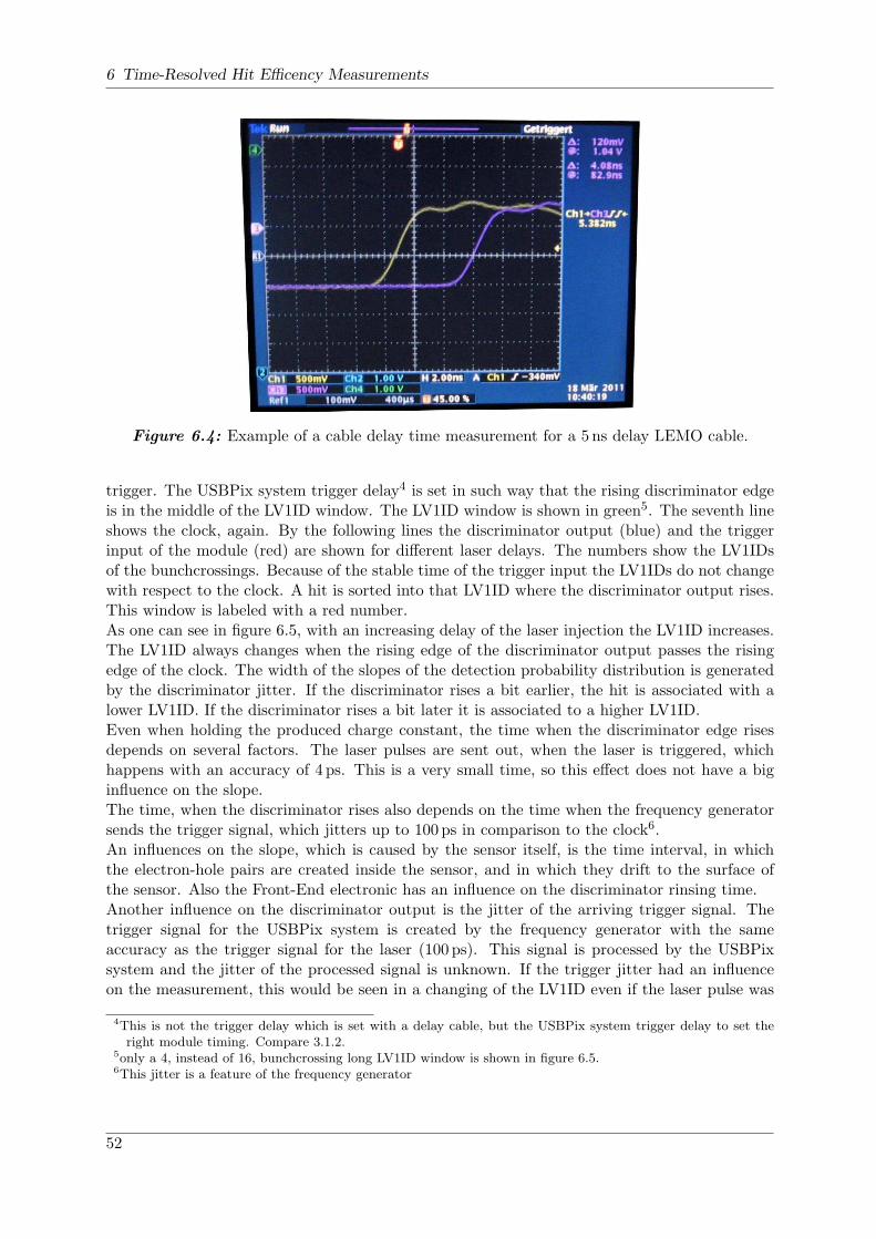
6 Time-Resolved Hit Efficency Measurements
Figure 6.4: Example of a cable delay time measurement for a 5 ns delay LEMO cable.
trigger. The USBPix system trigger delay4 is set in such way that the rising discriminator edgeis in the middle of the LV1ID window. The LV1ID window is shown in green5. The seventh lineshows the clock, again. By the following lines the discriminator output (blue) and the triggerinput of the module (red) are shown for different laser delays. The numbers show the LV1IDsof the bunchcrossings. Because of the stable time of the trigger input the LV1IDs do not changewith respect to the clock. A hit is sorted into that LV1ID where the discriminator output rises.This window is labeled with a red number.As one can see in figure 6.5, with an increasing delay of the laser injection the LV1ID increases.The LV1ID always changes when the rising edge of the discriminator output passes the risingedge of the clock. The width of the slopes of the detection probability distribution is generatedby the discriminator jitter. If the discriminator rises a bit earlier, the hit is associated with alower LV1ID. If the discriminator rises a bit later it is associated to a higher LV1ID.Even when holding the produced charge constant, the time when the discriminator edge risesdepends on several factors. The laser pulses are sent out, when the laser is triggered, whichhappens with an accuracy of 4 ps. This is a very small time, so this effect does not have a biginfluence on the slope.The time, when the discriminator rises also depends on the time when the frequency generatorsends the trigger signal, which jitters up to 100 ps in comparison to the clock6.An influences on the slope, which is caused by the sensor itself, is the time interval, in whichthe electron-hole pairs are created inside the sensor, and in which they drift to the surface ofthe sensor. Also the Front-End electronic has an influence on the discriminator rinsing time.Another influence on the discriminator output is the jitter of the arriving trigger signal. Thetrigger signal for the USBPix system is created by the frequency generator with the sameaccuracy as the trigger signal for the laser (100 ps). This signal is processed by the USBPixsystem and the jitter of the processed signal is unknown. If the trigger jitter had an influenceon the measurement, this would be seen in a changing of the LV1ID even if the laser pulse was
4This is not the trigger delay which is set with a delay cable, but the USBPix system trigger delay to set theright module timing. Compare 3.1.2.
5only a 4, instead of 16, bunchcrossing long LV1ID window is shown in figure 6.5.6This jitter is a feature of the frequency generator
52
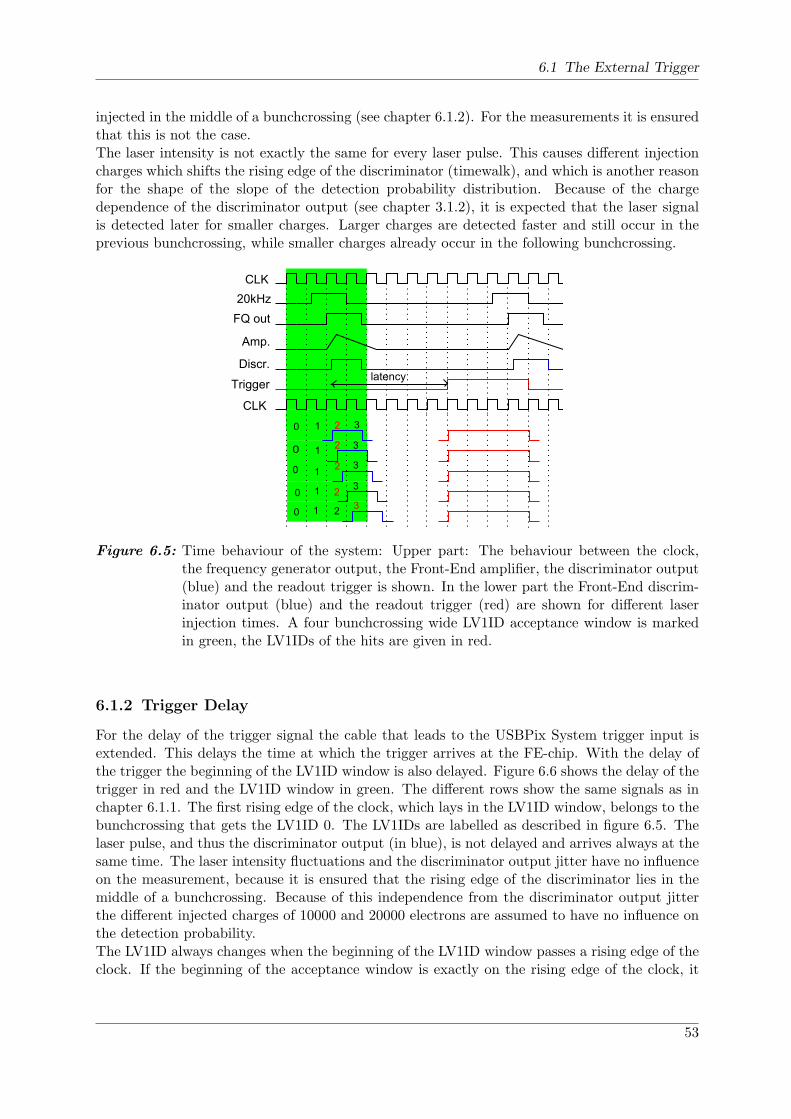
6.1 The External Trigger
injected in the middle of a bunchcrossing (see chapter 6.1.2). For the measurements it is ensuredthat this is not the case.The laser intensity is not exactly the same for every laser pulse. This causes different injectioncharges which shifts the rising edge of the discriminator (timewalk), and which is another reasonfor the shape of the slope of the detection probability distribution. Because of the chargedependence of the discriminator output (see chapter 3.1.2), it is expected that the laser signalis detected later for smaller charges. Larger charges are detected faster and still occur in theprevious bunchcrossing, while smaller charges already occur in the following bunchcrossing.
0
0
0
0 1 2 3
0 1
1
1
1
2
2
2
2
3
3
3
3
CLK
20kHz
FQ out
Amp.
Discr.
Trigger
CLK
latency
Figure 6.5: Time behaviour of the system: Upper part: The behaviour between the clock,the frequency generator output, the Front-End amplifier, the discriminator output(blue) and the readout trigger is shown. In the lower part the Front-End discrim-inator output (blue) and the readout trigger (red) are shown for different laserinjection times. A four bunchcrossing wide LV1ID acceptance window is markedin green, the LV1IDs of the hits are given in red.
6.1.2 Trigger Delay
For the delay of the trigger signal the cable that leads to the USBPix System trigger input isextended. This delays the time at which the trigger arrives at the FE-chip. With the delay ofthe trigger the beginning of the LV1ID window is also delayed. Figure 6.6 shows the delay of thetrigger in red and the LV1ID window in green. The different rows show the same signals as inchapter 6.1.1. The first rising edge of the clock, which lays in the LV1ID window, belongs to thebunchcrossing that gets the LV1ID 0. The LV1IDs are labelled as described in figure 6.5. Thelaser pulse, and thus the discriminator output (in blue), is not delayed and arrives always at thesame time. The laser intensity fluctuations and the discriminator output jitter have no influenceon the measurement, because it is ensured that the rising edge of the discriminator lies in themiddle of a bunchcrossing. Because of this independence from the discriminator output jitterthe different injected charges of 10000 and 20000 electrons are assumed to have no influence onthe detection probability.The LV1ID always changes when the beginning of the LV1ID window passes a rising edge of theclock. If the beginning of the acceptance window is exactly on the rising edge of the clock, it
53
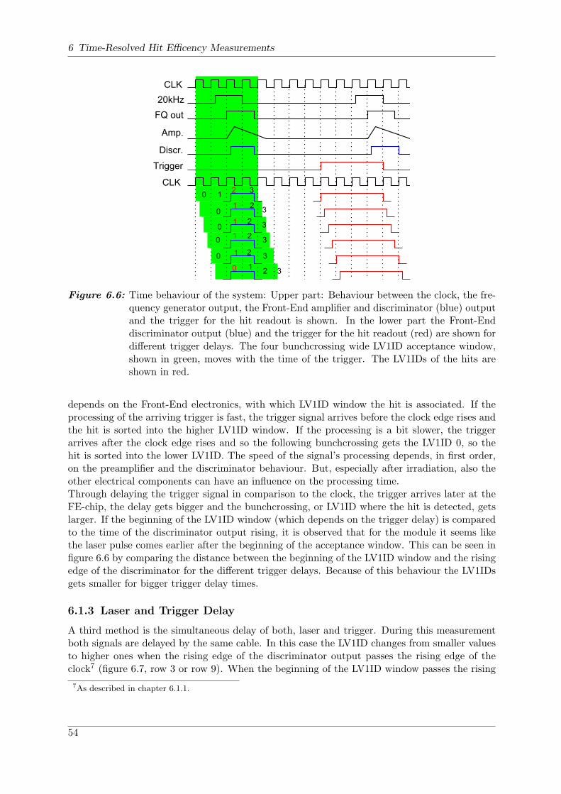
6 Time-Resolved Hit Efficency Measurements
0
1
2
3
0 12 3
0 1 2
0
0
0
1
1
2
2
2
1
3
3
3
3
CLK
20kHz
FQ out
Amp.
Discr.
Trigger
CLK
Figure 6.6: Time behaviour of the system: Upper part: Behaviour between the clock, the fre-quency generator output, the Front-End amplifier and discriminator (blue) outputand the trigger for the hit readout is shown. In the lower part the Front-Enddiscriminator output (blue) and the trigger for the hit readout (red) are shown fordifferent trigger delays. The four bunchcrossing wide LV1ID acceptance window,shown in green, moves with the time of the trigger. The LV1IDs of the hits areshown in red.
depends on the Front-End electronics, with which LV1ID window the hit is associated. If theprocessing of the arriving trigger is fast, the trigger signal arrives before the clock edge rises andthe hit is sorted into the higher LV1ID window. If the processing is a bit slower, the triggerarrives after the clock edge rises and so the following bunchcrossing gets the LV1ID 0, so thehit is sorted into the lower LV1ID. The speed of the signal’s processing depends, in first order,on the preamplifier and the discriminator behaviour. But, especially after irradiation, also theother electrical components can have an influence on the processing time.Through delaying the trigger signal in comparison to the clock, the trigger arrives later at theFE-chip, the delay gets bigger and the bunchcrossing, or LV1ID where the hit is detected, getslarger. If the beginning of the LV1ID window (which depends on the trigger delay) is comparedto the time of the discriminator output rising, it is observed that for the module it seems likethe laser pulse comes earlier after the beginning of the acceptance window. This can be seen infigure 6.6 by comparing the distance between the beginning of the LV1ID window and the risingedge of the discriminator for the different trigger delays. Because of this behaviour the LV1IDsgets smaller for bigger trigger delay times.
6.1.3 Laser and Trigger Delay
A third method is the simultaneous delay of both, laser and trigger. During this measurementboth signals are delayed by the same cable. In this case the LV1ID changes from smaller valuesto higher ones when the rising edge of the discriminator output passes the rising edge of theclock7 (figure 6.7, row 3 or row 9). When the beginning of the LV1ID window passes the rising
7As described in chapter 6.1.1.
54
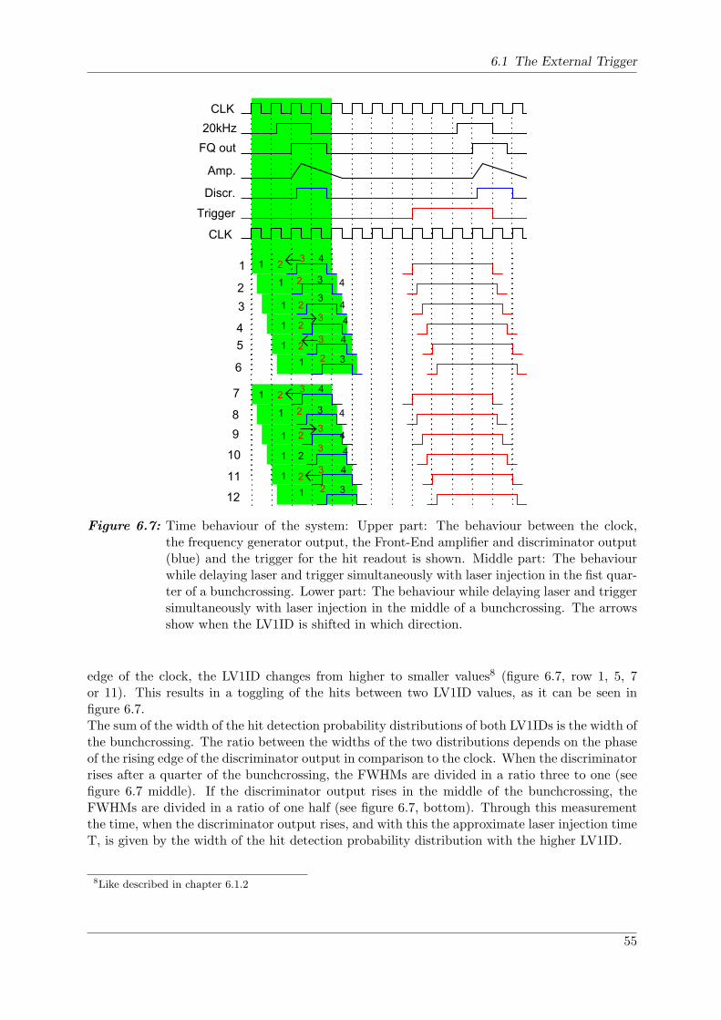
6.1 The External Trigger
1
1
1 1 1
1
1
1
1
3
41
2
2
2
2
2
3
3
3
3
3
2
4
4
4
4
1
1
1 1 1
1
1
1
1
3
41
2
2
2
2
2
3
3
3
3
3
2
4
4
4
4
CLK
20kHz
FQ out
Amp.
Discr.
Trigger
CLK
5
6
7
8
9
10
11
12
1
2
3
4
Figure 6.7: Time behaviour of the system: Upper part: The behaviour between the clock,the frequency generator output, the Front-End amplifier and discriminator output(blue) and the trigger for the hit readout is shown. Middle part: The behaviourwhile delaying laser and trigger simultaneously with laser injection in the fist quar-ter of a bunchcrossing. Lower part: The behaviour while delaying laser and triggersimultaneously with laser injection in the middle of a bunchcrossing. The arrowsshow when the LV1ID is shifted in which direction.
edge of the clock, the LV1ID changes from higher to smaller values8 (figure 6.7, row 1, 5, 7or 11). This results in a toggling of the hits between two LV1ID values, as it can be seen infigure 6.7.The sum of the width of the hit detection probability distributions of both LV1IDs is the width ofthe bunchcrossing. The ratio between the widths of the two distributions depends on the phaseof the rising edge of the discriminator output in comparison to the clock. When the discriminatorrises after a quarter of the bunchcrossing, the FWHMs are divided in a ratio three to one (seefigure 6.7 middle). If the discriminator output rises in the middle of the bunchcrossing, theFWHMs are divided in a ratio of one half (see figure 6.7, bottom). Through this measurementthe time, when the discriminator output rises, and with this the approximate laser injection timeT, is given by the width of the hit detection probability distribution with the higher LV1ID.
8Like described in chapter 6.1.2
55
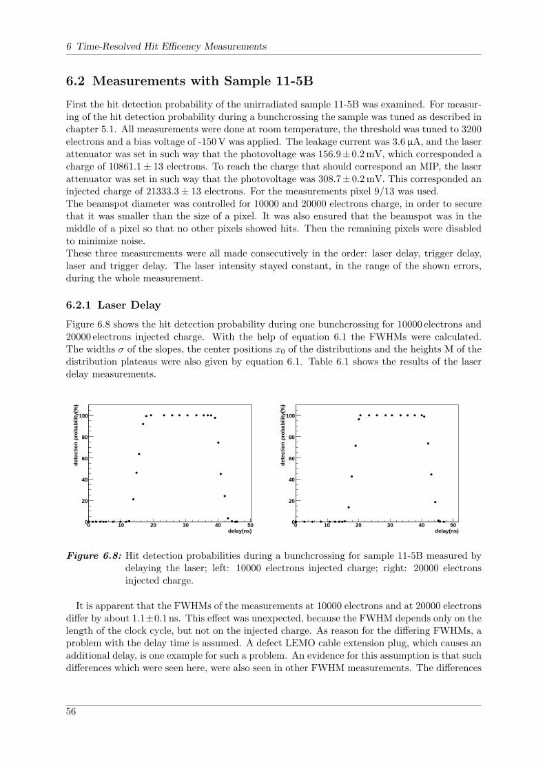
6 Time-Resolved Hit Efficency Measurements
6.2 Measurements with Sample 11-5B
First the hit detection probability of the unirradiated sample 11-5B was examined. For measur-ing of the hit detection probability during a bunchcrossing the sample was tuned as described inchapter 5.1. All measurements were done at room temperature, the threshold was tuned to 3200electrons and a bias voltage of -150V was applied. The leakage current was 3.6µA, and the laserattenuator was set in such way that the photovoltage was 156.9± 0.2mV, which corresponded acharge of 10861.1± 13 electrons. To reach the charge that should correspond an MIP, the laserattenuator was set in such way that the photovoltage was 308.7± 0.2mV. This corresponded aninjected charge of 21333.3± 13 electrons. For the measurements pixel 9/13 was used.The beamspot diameter was controlled for 10000 and 20000 electrons charge, in order to securethat it was smaller than the size of a pixel. It was also ensured that the beamspot was in themiddle of a pixel so that no other pixels showed hits. Then the remaining pixels were disabledto minimize noise.These three measurements were all made consecutively in the order: laser delay, trigger delay,laser and trigger delay. The laser intensity stayed constant, in the range of the shown errors,during the whole measurement.
6.2.1 Laser Delay
Figure 6.8 shows the hit detection probability during one bunchcrossing for 10000 electrons and20000 electrons injected charge. With the help of equation 6.1 the FWHMs were calculated.The widths σ of the slopes, the center positions x0 of the distributions and the heights M of thedistribution plateaus were also given by equation 6.1. Table 6.1 shows the results of the laserdelay measurements.
delay(ns)0 10 20 30 40 50
dete
ctio
n pr
obab
ility
(%)
0
20
40
60
80
100
delay(ns)0 10 20 30 40 50
dete
ctio
n pr
obab
ility
(%)
0
20
40
60
80
100
Figure 6.8: Hit detection probabilities during a bunchcrossing for sample 11-5B measured bydelaying the laser; left: 10000 electrons injected charge; right: 20000 electronsinjected charge.
It is apparent that the FWHMs of the measurements at 10000 electrons and at 20000 electronsdiffer by about 1.1±0.1 ns. This effect was unexpected, because the FWHM depends only on thelength of the clock cycle, but not on the injected charge. As reason for the differing FWHMs, aproblem with the delay time is assumed. A defect LEMO cable extension plug, which causes anadditional delay, is one example for such a problem. An evidence for this assumption is that suchdifferences which were seen here, were also seen in other FWHM measurements. The differences
56
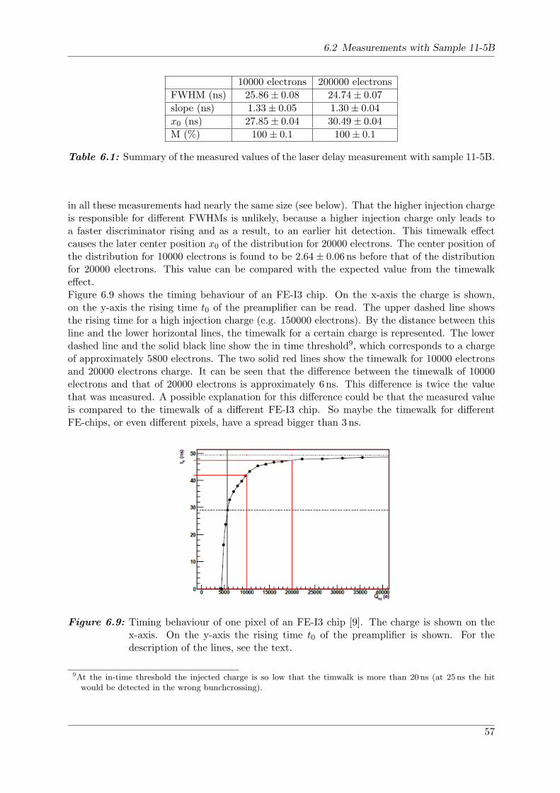
6.2 Measurements with Sample 11-5B
10000 electrons 200000 electrons
FWHM (ns) 25.86± 0.08 24.74± 0.07
slope (ns) 1.33± 0.05 1.30± 0.04
x0 (ns) 27.85± 0.04 30.49± 0.04
M (%) 100± 0.1 100± 0.1
Table 6.1: Summary of the measured values of the laser delay measurement with sample 11-5B.
in all these measurements had nearly the same size (see below). That the higher injection chargeis responsible for different FWHMs is unlikely, because a higher injection charge only leads toa faster discriminator rising and as a result, to an earlier hit detection. This timewalk effectcauses the later center position x0 of the distribution for 20000 electrons. The center position ofthe distribution for 10000 electrons is found to be 2.64± 0.06 ns before that of the distributionfor 20000 electrons. This value can be compared with the expected value from the timewalkeffect.Figure 6.9 shows the timing behaviour of an FE-I3 chip. On the x-axis the charge is shown,on the y-axis the rising time t0 of the preamplifier can be read. The upper dashed line showsthe rising time for a high injection charge (e.g. 150000 electrons). By the distance between thisline and the lower horizontal lines, the timewalk for a certain charge is represented. The lowerdashed line and the solid black line show the in time threshold9, which corresponds to a chargeof approximately 5800 electrons. The two solid red lines show the timewalk for 10000 electronsand 20000 electrons charge. It can be seen that the difference between the timewalk of 10000electrons and that of 20000 electrons is approximately 6 ns. This difference is twice the valuethat was measured. A possible explanation for this difference could be that the measured valueis compared to the timewalk of a different FE-I3 chip. So maybe the timewalk for differentFE-chips, or even different pixels, have a spread bigger than 3 ns.
Figure 6.9: Timing behaviour of one pixel of an FE-I3 chip [9]. The charge is shown on thex-axis. On the y-axis the rising time t0 of the preamplifier is shown. For thedescription of the lines, see the text.
9At the in-time threshold the injected charge is so low that the timwalk is more than 20 ns (at 25 ns the hitwould be detected in the wrong bunchcrossing).
57
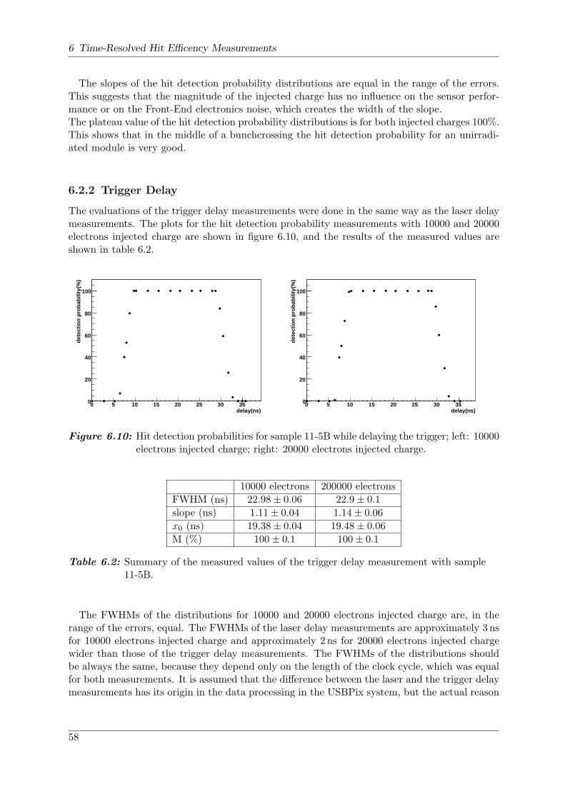
6 Time-Resolved Hit Efficency Measurements
The slopes of the hit detection probability distributions are equal in the range of the errors.This suggests that the magnitude of the injected charge has no influence on the sensor perfor-mance or on the Front-End electronics noise, which creates the width of the slope.The plateau value of the hit detection probability distributions is for both injected charges 100%.This shows that in the middle of a bunchcrossing the hit detection probability for an unirradi-ated module is very good.
6.2.2 Trigger Delay
The evaluations of the trigger delay measurements were done in the same way as the laser delaymeasurements. The plots for the hit detection probability measurements with 10000 and 20000electrons injected charge are shown in figure 6.10, and the results of the measured values areshown in table 6.2.
delay(ns)0 5 10 15 20 25 30 35
dete
ctio
n pr
obab
ility
(%)
0
20
40
60
80
100
delay(ns)0 5 10 15 20 25 30 35
dete
ctio
n pr
obab
ility
(%)
0
20
40
60
80
100
Figure 6.10: Hit detection probabilities for sample 11-5B while delaying the trigger; left: 10000electrons injected charge; right: 20000 electrons injected charge.
10000 electrons 200000 electrons
FWHM (ns) 22.98± 0.06 22.9± 0.1
slope (ns) 1.11± 0.04 1.14± 0.06
x0 (ns) 19.38± 0.04 19.48± 0.06
M (%) 100± 0.1 100± 0.1
Table 6.2: Summary of the measured values of the trigger delay measurement with sample11-5B.
The FWHMs of the distributions for 10000 and 20000 electrons injected charge are, in therange of the errors, equal. The FWHMs of the laser delay measurements are approximately 3 nsfor 10000 electrons injected charge and approximately 2 ns for 20000 electrons injected chargewider than those of the trigger delay measurements. The FWHMs of the distributions shouldbe always the same, because they depend only on the length of the clock cycle, which was equalfor both measurements. It is assumed that the difference between the laser and the trigger delaymeasurements has its origin in the data processing in the USBPix system, but the actual reason
58
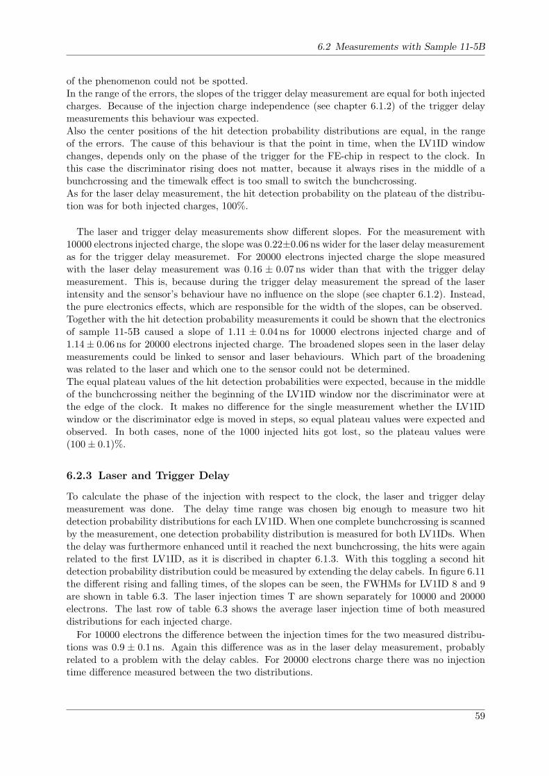
6.2 Measurements with Sample 11-5B
of the phenomenon could not be spotted.In the range of the errors, the slopes of the trigger delay measurement are equal for both injectedcharges. Because of the injection charge independence (see chapter 6.1.2) of the trigger delaymeasurements this behaviour was expected.Also the center positions of the hit detection probability distributions are equal, in the rangeof the errors. The cause of this behaviour is that the point in time, when the LV1ID windowchanges, depends only on the phase of the trigger for the FE-chip in respect to the clock. Inthis case the discriminator rising does not matter, because it always rises in the middle of abunchcrossing and the timewalk effect is too small to switch the bunchcrossing.As for the laser delay measurement, the hit detection probability on the plateau of the distribu-tion was for both injected charges, 100%.
The laser and trigger delay measurements show different slopes. For the measurement with10000 electrons injected charge, the slope was 0.22±0.06 ns wider for the laser delay measurementas for the trigger delay measuremet. For 20000 electrons injected charge the slope measuredwith the laser delay measurement was 0.16 ± 0.07 ns wider than that with the trigger delaymeasurement. This is, because during the trigger delay measurement the spread of the laserintensity and the sensor’s behaviour have no influence on the slope (see chapter 6.1.2). Instead,the pure electronics effects, which are responsible for the width of the slopes, can be observed.Together with the hit detection probability measurements it could be shown that the electronicsof sample 11-5B caused a slope of 1.11 ± 0.04 ns for 10000 electrons injected charge and of1.14± 0.06 ns for 20000 electrons injected charge. The broadened slopes seen in the laser delaymeasurements could be linked to sensor and laser behaviours. Which part of the broadeningwas related to the laser and which one to the sensor could not be determined.The equal plateau values of the hit detection probabilities were expected, because in the middleof the bunchcrossing neither the beginning of the LV1ID window nor the discriminator were atthe edge of the clock. It makes no difference for the single measurement whether the LV1IDwindow or the discriminator edge is moved in steps, so equal plateau values were expected andobserved. In both cases, none of the 1000 injected hits got lost, so the plateau values were(100± 0.1)%.
6.2.3 Laser and Trigger Delay
To calculate the phase of the injection with respect to the clock, the laser and trigger delaymeasurement was done. The delay time range was chosen big enough to measure two hitdetection probability distributions for each LV1ID. When one complete bunchcrossing is scannedby the measurement, one detection probability distribution is measured for both LV1IDs. Whenthe delay was furthermore enhanced until it reached the next bunchcrossing, the hits were againrelated to the first LV1ID, as it is discribed in chapter 6.1.3. With this toggling a second hitdetection probability distribution could be measured by extending the delay cabels. In figure 6.11the different rising and falling times, of the slopes can be seen, the FWHMs for LV1ID 8 and 9are shown in table 6.3. The laser injection times T are shown separately for 10000 and 20000electrons. The last row of table 6.3 shows the average laser injection time of both measureddistributions for each injected charge.
For 10000 electrons the difference between the injection times for the two measured distribu-tions was 0.9 ± 0.1 ns. Again this difference was as in the laser delay measurement, probablyrelated to a problem with the delay cables. For 20000 electrons charge there was no injectiontime difference measured between the two distributions.
59
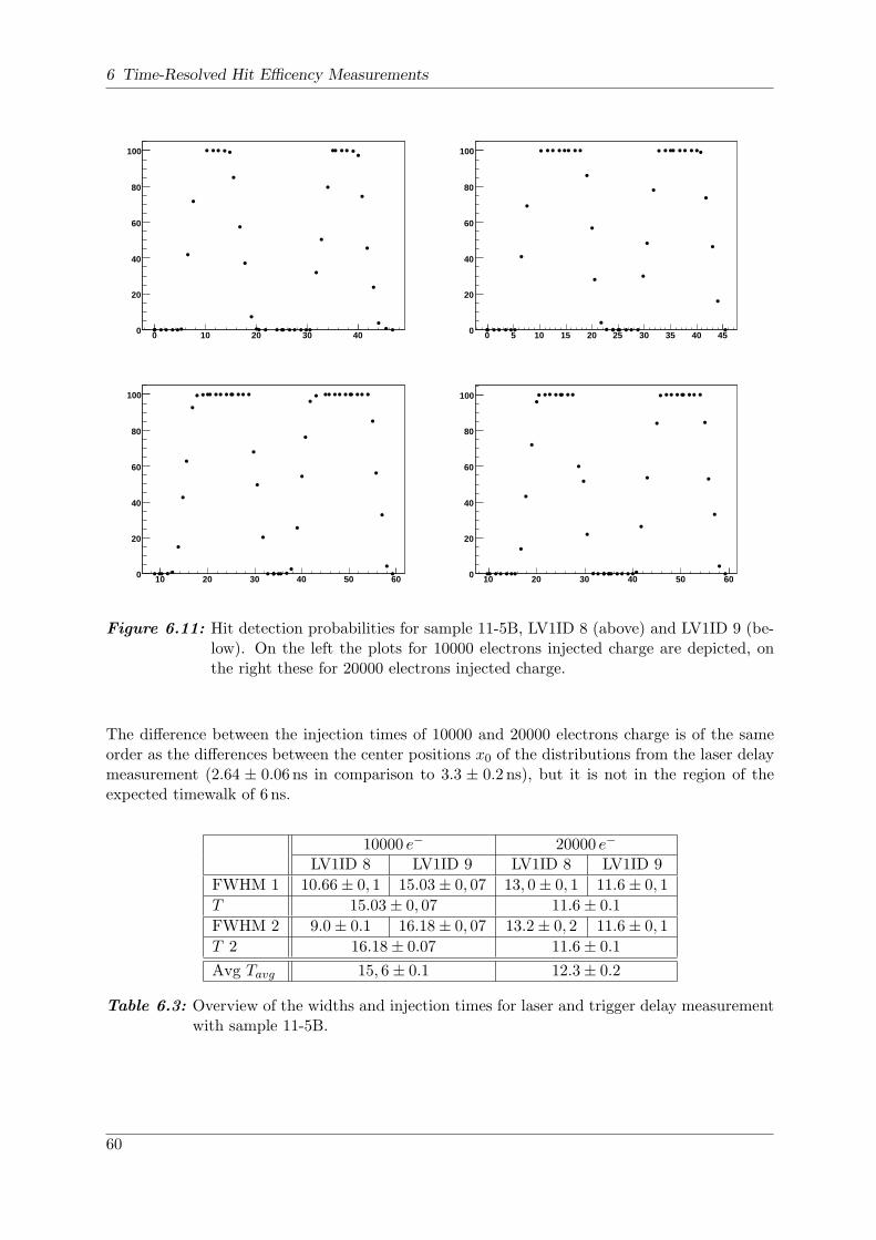
6 Time-Resolved Hit Efficency Measurements
0 10 20 30 400
20
40
60
80
100
0 5 10 15 20 25 30 35 40 450
20
40
60
80
100
10 20 30 40 50 600
20
40
60
80
100
10 20 30 40 50 600
20
40
60
80
100
Figure 6.11: Hit detection probabilities for sample 11-5B, LV1ID 8 (above) and LV1ID 9 (be-low). On the left the plots for 10000 electrons injected charge are depicted, onthe right these for 20000 electrons injected charge.
The difference between the injection times of 10000 and 20000 electrons charge is of the sameorder as the differences between the center positions x0 of the distributions from the laser delaymeasurement (2.64 ± 0.06 ns in comparison to 3.3 ± 0.2 ns), but it is not in the region of theexpected timewalk of 6 ns.
10000 e− 20000 e−
LV1ID 8 LV1ID 9 LV1ID 8 LV1ID 9
FWHM 1 10.66± 0, 1 15.03± 0, 07 13, 0± 0, 1 11.6± 0, 1
T 15.03± 0, 07 11.6± 0.1
FWHM 2 9.0± 0.1 16.18± 0, 07 13.2± 0, 2 11.6± 0, 1
T 2 16.18± 0.07 11.6± 0.1
Avg Tavg 15, 6± 0.1 12.3± 0.2
Table 6.3: Overview of the widths and injection times for laser and trigger delay measurementwith sample 11-5B.
60
6.3 Measurements with Sample 4-6B
6.3 Measurements with Sample 4-6B
The same measurements that were done with sample 11-5B were also done with sample 4-6B,so it was also tuned to a threshold of 3200 electrons, like it was described in chapter 5.2. Tominimize the leakage current, the chuck temperature was set at -40C, which corresponded asensor temperature of approximately10 -25C. The bias voltage was set to -600V, and the leakagecurrent was approximately 2.16µA.Before the beginning of the measurements it was ensured that the beamspot diameter wassmaller than the size of a pixel. Thus it was made sure that the whole charge was injected intoone pixel. This was successfully checked by a test measurement, where only the pixel which wasilluminated by the laser beam showed hits.Again, pixel 9/13 was used, for the measurements, all other pixels were disabled. First, themeasurements with 10000 electrons injected charge were made with each of the three differentdelay types, then those with 20000 electrons followed. At the beginning of the measurementswith 10000 electrons, the NTC installed at the attachment structure of the single chip cardshowed a temperature of (−24 ± 1)C. The voltage of the photodiode was 160.5 ± 1.5mVduring the whole measurement, which corresponds to a charge of 11118± 104 electrons. At thebeginning of the measurement with the injection charge of 20000 electrons, the temperature was(−25 ± 1)C, during the whole measurement the photovoltage had the value 311.3 ± 0.4mV.That corresponds to a charge of 21583.3± 27.7 electrons.
6.3.1 Laser Delay
Table 6.4 shows the results of the laser delay measurement, and figure 6.12 shows the corre-sponding hit detection probability distributions.
10000 electrons 200000 electrons
FWHM (ns) 24.90± 0.06 24.86± 0.07
slope (ns) 1.89± 0.04 1.78± 0.05
x0 (ns) 23.53± 0.04 23.51± 0.04
M (%) 98.0± 0.2 98.4± 0.2
Table 6.4: Summary of the measured values of the laser delay measurement with sample 4-6B.
The FWHMs of the hit detection probability distributions are, for 10000 and 20000 electronsinjection charge, in the range of the errors, equal. This was expected (see chapter 6.1.2) andsupports the assumption that the different FWHMs of the laser delay measurement with sample11-5B are caused by a parasitic error.The measurement results for the slopes for 10000 and 20000 electrons injected charge are slightlydifferent. This small difference of 110 ± 60 ps can be interpreted as a small injection chargedependence of the slope, but it can also be interpreted as outer or as statistical influences onthe measurement. For a charge dependency of the slope, no cause could be found, so the secondinterpretation seems the more likely one.The center positions of the hit detection probability distributions are equal in the range of theerrors. Because of the timewalk effect, they were expected to have a difference of 6 ns. Anexplanation for the equal center positions might be some influence of the irradiation. If in
10The temperature was measured with the NTC that was installed at the attachment of the single chip card.
61

6 Time-Resolved Hit Efficency Measurements
delay(ns)0 10 20 30 40 50
dete
ctio
n pr
obab
ility
(%)
0
20
40
60
80
100
delay(ns)0 10 20 30 40 50
dete
ctio
n pr
obab
ility
(%)
0
20
40
60
80
100
Figure 6.12: Hit detection probabilities for sample 4-6B while delaying the laser; left: 10000electrons injected charge; right: 20000 electrons injected charge.
an irradiated FE-chip also bigger charges were detected more slowly, the timewalk differencesbetween 10000 and 20000 electrons injected charge would have a smaller relativ effect.The hit detection probabilities on the plateaus of the distributions are very similar for bothinjected charges, but that one of 20000 electrons is (0.4± 0.3)% higher. The lower the injectedcharges are the likelier it is that the number of electron-hole pairs is no longer high enough toexceed the discriminator threshold. Recombination of electron-hole pairs as well as trapping11
caused by irradiation can lower the number of free charge carriers. This explains why the hitdetection probability of an irradiated sample is bigger for high injection charges.
6.3.2 Trigger Delay
Table 6.5 and figure 6.13 show the results of the trigger delay measurements for sample 4-6B.
10000 electrons 200000 electrons
FWHM (ns) 24.06± 0.08 22.00± 0.08
slope (ns) 1.14± 0.05 1.03± 0.05
x0 (ns) 19.80± 0.04 18.75± 0.05
M (%) 98.7± 0.4 99.0± 0.1
Table 6.5: Summary of the measured values of the trigger delay measurement with sample4-6B.
During these measurements the hit detection probability distributions start rising at thesame delay time (≈ 5 ns) for both injected charges, but the distribution for 20000 electronsinjected charge falls to zero again 2 ns earlier than the distribution for 10000 electrons (32 nsin comparison to 34 ns delay time). This results in a 2 ns shorter FWHM and a 1 ns earliercenter position for the detection probability distribution of 20000 electrons injected charge.Such an effect was not seen during the measurements with sample 11-5B, nor during the laser
11Irradiation causes additional energy levels inside the sensor lattice. These energy levels can capture electronsor holes so that these are no longer available for a sensor signal. Instead electrons and holes are released afterseveral µs and get lost for the signal. This effect is called ”trapping”.
62
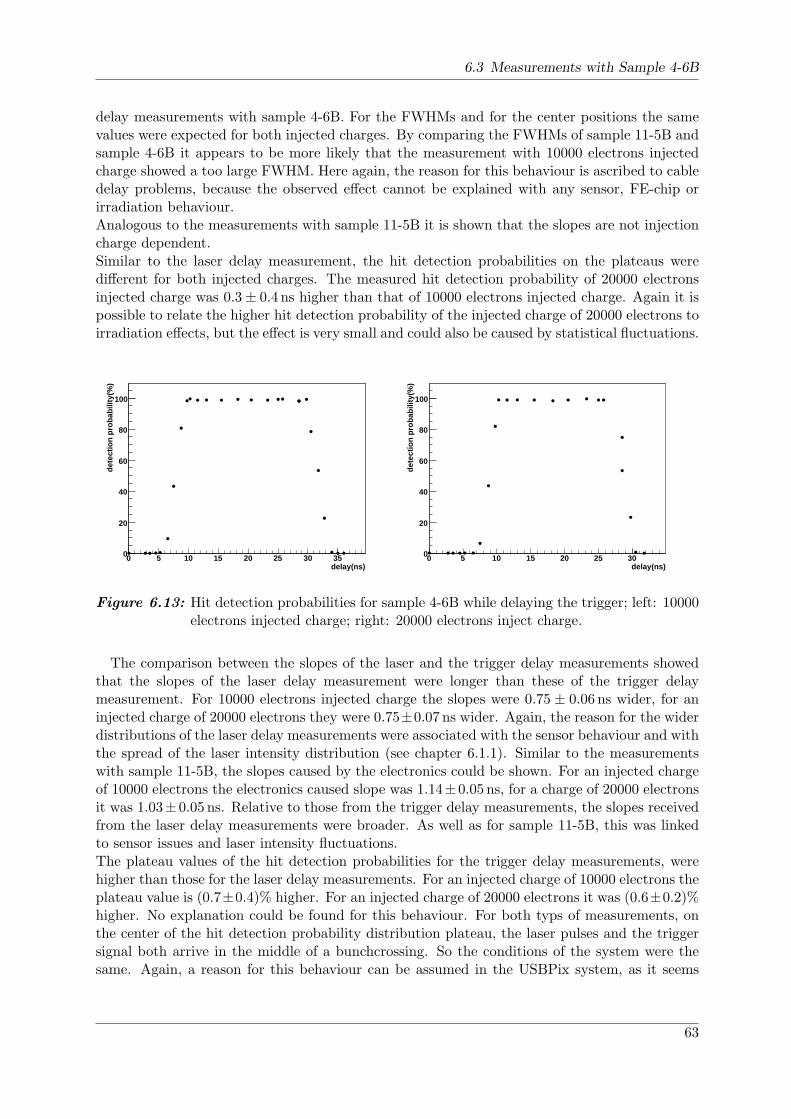
6.3 Measurements with Sample 4-6B
delay measurements with sample 4-6B. For the FWHMs and for the center positions the samevalues were expected for both injected charges. By comparing the FWHMs of sample 11-5B andsample 4-6B it appears to be more likely that the measurement with 10000 electrons injectedcharge showed a too large FWHM. Here again, the reason for this behaviour is ascribed to cabledelay problems, because the observed effect cannot be explained with any sensor, FE-chip orirradiation behaviour.Analogous to the measurements with sample 11-5B it is shown that the slopes are not injectioncharge dependent.Similar to the laser delay measurement, the hit detection probabilities on the plateaus weredifferent for both injected charges. The measured hit detection probability of 20000 electronsinjected charge was 0.3± 0.4 ns higher than that of 10000 electrons injected charge. Again it ispossible to relate the higher hit detection probability of the injected charge of 20000 electrons toirradiation effects, but the effect is very small and could also be caused by statistical fluctuations.
delay(ns)0 5 10 15 20 25 30 35
dete
ctio
n pr
obab
ility
(%)
0
20
40
60
80
100
delay(ns)0 5 10 15 20 25 30
dete
ctio
n pr
obab
ility
(%)
0
20
40
60
80
100
Figure 6.13: Hit detection probabilities for sample 4-6B while delaying the trigger; left: 10000electrons injected charge; right: 20000 electrons inject charge.
The comparison between the slopes of the laser and the trigger delay measurements showedthat the slopes of the laser delay measurement were longer than these of the trigger delaymeasurement. For 10000 electrons injected charge the slopes were 0.75 ± 0.06 ns wider, for aninjected charge of 20000 electrons they were 0.75±0.07 ns wider. Again, the reason for the widerdistributions of the laser delay measurements were associated with the sensor behaviour and withthe spread of the laser intensity distribution (see chapter 6.1.1). Similar to the measurementswith sample 11-5B, the slopes caused by the electronics could be shown. For an injected chargeof 10000 electrons the electronics caused slope was 1.14±0.05 ns, for a charge of 20000 electronsit was 1.03± 0.05 ns. Relative to those from the trigger delay measurements, the slopes receivedfrom the laser delay measurements were broader. As well as for sample 11-5B, this was linkedto sensor issues and laser intensity fluctuations.The plateau values of the hit detection probabilities for the trigger delay measurements, werehigher than those for the laser delay measurements. For an injected charge of 10000 electrons theplateau value is (0.7±0.4)% higher. For an injected charge of 20000 electrons it was (0.6±0.2)%higher. No explanation could be found for this behaviour. For both typs of measurements, onthe center of the hit detection probability distribution plateau, the laser pulses and the triggersignal both arrive in the middle of a bunchcrossing. So the conditions of the system were thesame. Again, a reason for this behaviour can be assumed in the USBPix system, as it seems
63
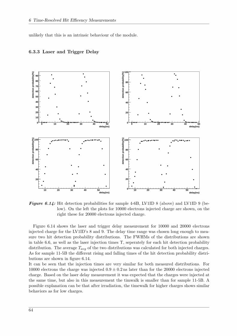
6 Time-Resolved Hit Efficency Measurements
unlikely that this is an intrinsic behaviour of the module.
6.3.3 Laser and Trigger Delay
delay(ns)0 10 20 30 40 50
dete
ctio
n pr
obab
ility
(%)
0
10
20
30
40
50
60
70
80
90
delay(ns)0 10 20 30 40 50
dete
ctio
n pr
obab
ility
(%)
0
20
40
60
80
100
delay(ns)10 20 30 40 50
dete
ctio
n pr
obab
ility
(%)
20
40
60
80
100
delay(ns)10 20 30 40 50
dete
ctio
n pr
obab
ility
(%)
0
20
40
60
80
100
Figure 6.14: Hit detection probabilities for sample 4-6B, LV1ID 8 (above) and LV1ID 9 (be-low). On the left the plots for 10000 electrons injected charge are shown, on theright these for 20000 electrons injected charge.
Figure 6.14 shows the laser and trigger delay measurement for 10000 and 20000 electronsinjected charge for the LV1ID’s 8 and 9. The delay time range was chosen long enough to mea-sure two hit detection probability distributions. The FWHMs of the distributions are shownin table 6.6, as well as the laser injection times T, seperately for each hit detection probabilitydistribution. The average Tavg of the two distributions was calculated for both injected charges.As for sample 11-5B the different rising and falling times of the hit detection probability distri-butions are shown in figure 6.14.It can be seen that the injection times are very similar for both measured distributions. For10000 electrons the charge was injected 0.9 ± 0.2 ns later than for the 20000 electrons injectedcharge. Based on the laser delay measurement it was expected that the charges were injected atthe same time, but also in this measurement the timwalk is smaller than for sample 11-5B. Apossible explanation can be that after irradiation, the timewalk for higher charges shows similarbehaviors as for low charges.
64

6.4 Comparison of the Samples
10000 e− 20000 e−
LV1ID 8 LV1ID 9 LV1ID 8 LV1ID 9
Width 1 4.5± 0, 2 19.8± 0, 2 6, 4± 0, 3 18.7± 0, 2
T 19.8± 0, 2 18.7± 0.2
Width 2 5.3± 0.1 19.44± 0, 08 6.4± 0, 2 18.7± 0, 2
T 2 19.44± 0.08 18.7± 0.2
Avg Tavg 19, 6± 0.2 18.7± 0.3
Table 6.6: Overview of the widths and injection times for the laser and trigger delay measure-ments with sample 4-6B.
6.4 Comparison of the Samples
6.4.1 Hit Detection Probabilities Distribution Slopes
Table 6.7 shows the measured slopes for sample 11-5B and sample 4-6B. Additionally, thecalculated differences between the slopes of both samples are shown. It is apparent that theslopes of sample 4-6B, which were measured in the laser delay measurements, were wider thanthose of sample 11-5B. For an injected charge of 10000 electrons they were 0.56± 0.06 ns wider,for 20000 electrons injected charge they were 0.48 ± 0.06 ns wider. The cause for this increaseof the slopes was the irradiation of sample 4-6B. Responsible for the width of the slopes arethe spread of the laser intensity distribution, the spread of the charge signal, which comes fromthe sensor, and the behaviour of the FE-electronics as well. The spread of the laser intensitydistribution is independent from the sample so this could not be the wider slopes’ cause. Thespreads difference between the slopes was thus created by the Front-End electronics and thesensor behaviours.
slope [ns]
Injected charge 11-5B 4-6B Difference
Laser delay10000 e− 1.33± 0.05 1.89± 0.04 0.56± 0.0620000 e− 1.30± 0.04 1.78± 0.05 0.48± 0.09
Trigger delay10000 e− 1.11± 0.04 1.14± 0.05 0.03± 0.0620000 e− 1.14± 0.06 1.03± 0.05 −0.11± 0.08
Difference10000 e− 0.22± 0.06 0.75± 0.06 0.53± 0.820000 e− 0.16± 0.07 0.75± 0.07 0.6± 0.1
Table 6.7: Measured slopes for sample 11-5B and sample 4-6B with the different delay types.The bottom row shows the differences between the slopes that were measured withthe laser delay measurement and these measured with the trigger delay measure-ment. The last column shows the slope differences between sample 11-5B and sample4-6B.
The wider slopes of the irradiated sample result in the fact that the interval in which a hit canbe related to two bunchcrossings, is increased. If a charge is injected during this time interval,it cannot be decided to which bunchcrossing it belongs.
65
6 Time-Resolved Hit Efficency Measurements
The slopes of sample 11-5B and sample 4-6B, which were measured with the trigger delaymeasurements, were nearly equal. For an injected charge of 10000 electrons the slopes were,in the range of the errors, the same, the difference was calculated as 0.03 ± 0.06 ns. For 20000electrons injected charge the slopes of sample 11-5B were larger than these of sample 4-6B,the difference here was 0.11 ± 0.07 ns. It is apparent from the slope differences between bothsamples that the irradiation did not broaden the slopes. The widths of the slopes depend on theclock, the beginning of the acceptance window and the electronics. Neither the clock nor thebeginning of the acceptance window, which means the time of the trigger input, are influencedby the irradiation. So the behaviour of the slopes resulted only from the FE-electronics andhere no worsening was observed. As described above, sensor behaviours had no influence on thismeasurement.
In chapter 6.2 and 6.3 the differences between the slopes of the laser delay measurementsand of the trigger delay measurements were calculated. They are shown in the bottom row oftable 6.7, too. These differences gave an upper limit on that part of the slope that was createdby the sensor behaviours. Because the laser intensity fluctuations are independent from the usedmodule, the difference between these values show the changing of the sensor performance. Foran injected charge of 10000 electrons the difference was 0.53 ± 0.08 ns, and for 20000 electronsit was 0.6 ± 0.1 ns. This result shows that the irradiation of the sensor broadens the slopes ofthe hit detection probability distributions. The calculated values were equal for both injectedcharges, so it seems that this effect is not injection charge dependent.
6.4.2 Hit Efficiency Measurement in the Middle of a Bunchcrossing
The plateau heights for sample 11-5B were (100±0.1)% for both injected charges and both delaytypes (laser and trigger delay). This means that in the middle of a bunchcrossing every injectedcharge was detected. For sample 4-6B, however, the detection probability on the plateau wassmaller than 100% for both injected charges and both delay types (see table 6.8). This suggeststhat the hit detection probability of the sample was diminished by irradiation. A hit detectionprobability of approximately 98% was also seen before at samples which were irradiated with asimilar dose [45].
Plateau high in [%]
Injected charge 11-5B 4-6B Difference
Laser delay measurement10000 e− 100± 0.1 98.0± 0.02 2.0± 0.220000 e− 100± 0.1 98.4± 0.2 1.6± 0.02
Trigger delay measurement10000 e− 100± 0.1 98.7± 0.04 1.3± 0.420000 e− 100± 0.1 99.0± 0.1 1.0± 0.01
Table 6.8: Plateau values for the hit detection probabilities with samples 11-5B and 4-6B. Alsoshown are the differences between both modules.
6.4.3 Timing and Timewalk
Table 6.9 gives an overview of the injection times Tinj and the laser delay measurement centerpositions x0 for sample 11-5B and sample 4-6B. Additionally shown is the calculated timewalk,which shows for both methods an irradiation dependency. The measurements show, that the
66
6.5 Conclusion
timewalk is smaller when the sensor is irradiated. A possible explanation can be that, byirradiation, the worsening of the preamplifier behaviours is more distinct for high charges. Thisassumption can be proven by redoing the plot of figure 6.9 with an irradiated sample. Thedescribed behaviour would appear in a graph that has a similar shape as the old one, but witha lower maximum.
Injected charge 11-5B 4-6B
Tavg [ns]10000 e− 15.6± 0.1 19.6± 0.220000 e− 12.3± 0.2 18.7± 0.3
Timewalk 3.3± 0.2 0.9± 0.4
x0 [ns]10000 e− 27.85± 0.04 23.51± 0.420000 e− 30.49± 0.04 23.53± 0.1
Timewalk 2.64± 0.06 0.02± 0.04
Table 6.9: Comparison of the laser injection times: Laser injection time from the trigger andlaser delay measurements and center position from the laser delay measurementswith sample 11-5B and sample 4-6B. The calculated timewalk is shown too.
6.5 Conclusion
Considering the results it can be stated that the hit detection probability measurements showedseveral unexpected effects, which could not be explained with sensor or Front-End effects. Mostof them were ascribed to problems with the setting of the delay times. It is guessed that a LEMOcable extension was not working well and that this caused an extra delay. This suggestion issupported by the fact that all of the strange measurements had too long delay times. Theseeffects were especially seen in the FWHMs and in the center positions x0. To prevent thosedelay time problems, in an improved measurement the delay could be done with an frequencygenerator and instead of delay cables. This would give more exact delay times, and delay timeerrors would be prevented.One result of the measurements is that the timewalk gets smaller when the sensor is irradiated.This effect was observed at the laser and trigger delay measurement and at the center positionsmeasurement of the laser delay measurements. In both cases a clear effect was seen, which isan evidence that the effect is not caused by parasitic errors. But because of the delay timeuncertainties, further measurements have to be done to make a final statement about the sizeof this effect.The hit detection probability distribution slope measurements showed clear results. It could beshown, that the irradiation of the FE-chip has nearly no influence on the width of the slope.It could also be shown, that the widening of the slopes, in the laser delay measurements, afterirradiation is related to sensor issues. The effect itself was, with the whole ATLAS lifetime dose,causing a widening of approximately 0.5 ns, still small.The hit detection efficiency on the plateau of the distribution differed between samples 11-5Band 4-6B by about 1 to 2%. For sample 4-6B a very small charge dependency of the hit detectionefficiency could be shown. Nevertheless the hit detection efficiency of approximately 98% afterthe irradiation with the ATLAS lifetime dose showed the expected value.
67


7 Hit Induced Noise
The aim of the measurements that are shown in this chapter was to determine if injecting hitsinto the sensor increases the noise of the module. For this reason the hit occupancy, which isdefined as the number of hits per bunchcrossing and pixel, was calculated. This can be done bymeasuring the hitbus rate. With a BK Precision 4085 40MHz Arbitrary/Function Generatorwith counter, the positive hitbus slopes within a measurement time t=5 minutes were counted.With this rate N the hit occupancy O can be calculated by
O =N/t
P· 25ns (7.1)
where P is the number of module pixels. For single chip sensors, which where used for thesemeasurements, P=2880. For the calculation of the hit induced noise occupancy, measurementswere done while the sensor was irradiated with an Americium 241 source and without a source.The experiments are based on several assumptions. For the measurement with a source it wasassumed that for a high threshold the hit occupancy Ohigh is created by two parts. The first partis the noise occupancy Ohigh,noise. It is created by the noise of the module. The discriminatorthreshold is more often exceeded by the noise of the analogue part of the read out chain whenthe threshold is low than when it is high. So at a high threshold the noise occupancy is low andit increases when decreasing the threshold. The second part of the hit occupancy Ohigh,source iscreated by the hits that are produced by the Americium source.For a low threshold it was assumed that the hit occupancy Olow is created by three parts. Thefirst two are the same as at the high threshold: Olow,noise for the noise occupancy without asource and Olow,source for the occupancy that is created by the source1. The third part is thehit induced noise occupancy Ohitnoise.
Ohigh = Ohigh,noise +Ohigh,source (7.2)
Olow = Olow,noise +Olow,source +Ohitnoise (7.3)
Ohigh,noise can be measured at a high threshold without a source. With a second measurement ata high threshold, but with the source, the sum of the source occupancy and the noise occupancyOhigh can be measured.Likewise, at the low threshold Olow,noise can be measured without a source and Olow with thesource. With these four measurements the hit induced noise occupancy is calculated:
Ohitnoise = Olow −Olow,noise − (Ohigh −Ohigh,noise) (7.4)
For the calculation of the hit induced noise occupancy each measurement was done ten times. Ashigh threshold 4000 electrons were chosen. As low thresholds 2500 electrons, 2100 electrons andthe threshold of the incremental threshold scan (see below) were chosen. With these thresholdsa possible threshold dependency of the hit induced noise can be shown.
1The rate of the source does not depend on the threshold Olow,source = Ohigh,source.
69
7 Hit Induced Noise
Incremental Threshold Scan
With the incremental threshold scan the minimal threshold at which measurements are still pos-sible, is found. For this reason a special tuning procedure was implemented where the T-DACvalues are decreased individually for each pixel. After the T-DAC value is decreased a thresholdscan is done and the noise of the threshold (see chapter3.1.2) σ is checked. If σ is smaller than aset cut value, the scan is considered successfully, if it is larger the scan failed. This noise cut canbe set manually separately for normal, long, ganged and inter-ganged pixels. The cuts shown intable 7.1 where used for sample 11-5B.In the beginning of the tuning procedure the T-DAC values are decreased by five digital units(DU). If the scan is considered successfully, the T-DAC is again decreased by five DU. If thenoise is to high, the scan failed and the T-DAC is increased by five DU. Then the step size isreduced by one and the T-DAC is decreased again. This procedure is done until the minimalpossible T-DAC value for every pixel is found.After this scanning procedure all T-DAC values are increased by one. This step is done to geta more stably working module. With this incremental threshold scan the minimal threshold ofthe module can be found. After the whole scanning procedure a threshold scan is done to findthe threshold of the module. For the used sample 11-5B the minimal threshold was 1900± 25.8electrons with a noise σ of 238± 27.59 electrons.
Pixel type normal long ganged inter-ganged
Cut [e] 300 350 450 350
Table 7.1: Noise cuts for the incremental threshold scan.
Hitbus Measurements
With the USBPix system it is possible to measure the hitbus signal by connecting the counterto a LEMO connector. The counter measures the number of positive hitbus slopes. At a mea-surement without a source, on a high threshold (e. g. 4000 electrons), there are nearly no noisehits. Only hits from cosmic muons are expected. With the source, the pure source rate shouldbe measured, except a small contribution from cosmic muons.Approximately 10000 muons per square meter and minute reach the surface of the earth [46].For the senor area of approximately 0.6 cm2 0.62 muons are expected in one minute. This resultsin 3.1 muons for a measurement time of five minutes. The average of ten measurements witha threshold of 4000 electrons and without a source gives 3.8 ± 0.7 muons within five minutes.That shows that at a threshold of 4000 electrons, nearly no noise hits are created.Figure 7.1 shows that the plotted noise occupancy increases, when the threshold is reduced.Furthermore, it is shown that for a certain threshold the noise level fluctuates very strongly.The measurements illustrated by red circles and pink triangles were done with sample 11-5B.The red circles show the average values of ten measurements. These were the measurementsthat were used to calculate the hit induced noise occupancy. The pink triangles show singlemeasurements that were recorded with another module configuration. Finally, the blue squaresshow measurements [46] that were recorded with a different single chip card. It can be seen thatfor similar thresholds the occupancies differ a lot, even if the same sample and configuration isobserved. The large fluctuations in the occupancy are related to different external parameters
70
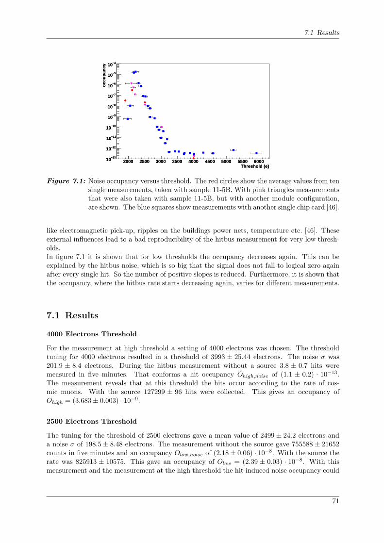
7.1 Results
Threshold (e)2000 2500 3000 3500 4000 4500 5000 5500 6000
occu
panc
y
−1310
−1210
−1110
−1010
−910
−810
−710
−610
−510
−410
Threshold (e)2000 2500 3000 3500 4000 4500 5000 5500 6000
occu
panc
y
−1310
−1210
−1110
−1010
−910
−810
−710
−610
−510
−410
Figure 7.1: Noise occupancy versus threshold. The red circles show the average values from tensingle measurements, taken with sample 11-5B. With pink triangles measurementsthat were also taken with sample 11-5B, but with another module configuration,are shown. The blue squares show measurements with another single chip card [46].
like electromagnetic pick-up, ripples on the buildings power nets, temperature etc. [46]. Theseexternal influences lead to a bad reproducibility of the hitbus measurement for very low thresh-olds.In figure 7.1 it is shown that for low thresholds the occupancy decreases again. This can beexplained by the hitbus noise, which is so big that the signal does not fall to logical zero againafter every single hit. So the number of positive slopes is reduced. Furthermore, it is shown thatthe occupancy, where the hitbus rate starts decreasing again, varies for different measurements.
7.1 Results
4000 Electrons Threshold
For the measurement at high threshold a setting of 4000 electrons was chosen. The thresholdtuning for 4000 electrons resulted in a threshold of 3993 ± 25.44 electrons. The noise σ was201.9 ± 8.4 electrons. During the hitbus measurement without a source 3.8 ± 0.7 hits weremeasured in five minutes. That conforms a hit occupancy Ohigh,noise of (1.1 ± 0.2) · 10−13.The measurement reveals that at this threshold the hits occur according to the rate of cos-mic muons. With the source 127299 ± 96 hits were collected. This gives an occupancy ofOhigh = (3.683± 0.003) · 10−9.
2500 Electrons Threshold
The tuning for the threshold of 2500 electrons gave a mean value of 2499 ± 24.2 electrons anda noise σ of 198.5 ± 8.48 electrons. The measurement without the source gave 755588 ± 21652counts in five minutes and an occupancy Olow,noise of (2.18± 0.06) · 10−8. With the source therate was 825913 ± 10575. This gave an occupancy of Olow = (2.39 ± 0.03) · 10−8. With thismeasurement and the measurement at the high threshold the hit induced noise occupancy could
71
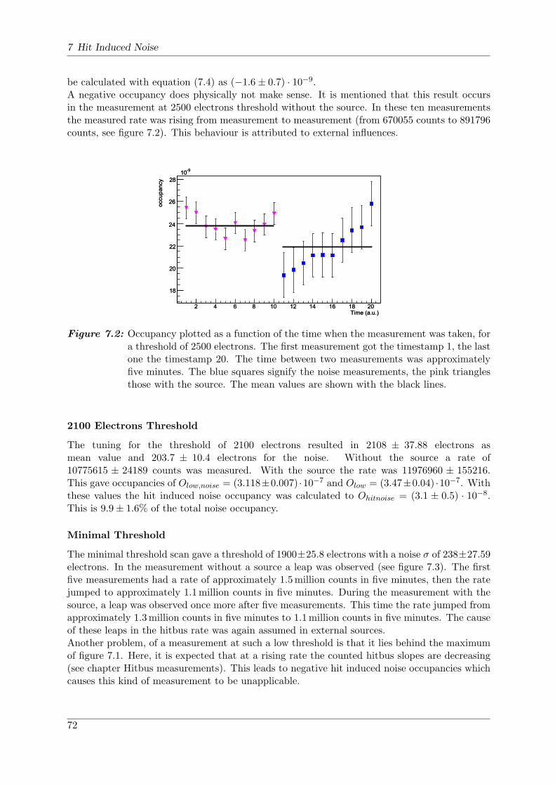
7 Hit Induced Noise
be calculated with equation (7.4) as (−1.6± 0.7) · 10−9.A negative occupancy does physically not make sense. It is mentioned that this result occursin the measurement at 2500 electrons threshold without the source. In these ten measurementsthe measured rate was rising from measurement to measurement (from 670055 counts to 891796counts, see figure 7.2). This behaviour is attributed to external influences.
Time (a.u.)2 4 6 8 10 12 14 16 18 20
occu
pa
ncy
18
20
22
24
26
28
-910
Time (a.u.)2 4 6 8 10 12 14 16 18 20
occu
pa
ncy
18
20
22
24
26
28
-910
Figure 7.2: Occupancy plotted as a function of the time when the measurement was taken, fora threshold of 2500 electrons. The first measurement got the timestamp 1, the lastone the timestamp 20. The time between two measurements was approximatelyfive minutes. The blue squares signify the noise measurements, the pink trianglesthose with the source. The mean values are shown with the black lines.
2100 Electrons Threshold
The tuning for the threshold of 2100 electrons resulted in 2108 ± 37.88 electrons asmean value and 203.7 ± 10.4 electrons for the noise. Without the source a rate of10775615 ± 24189 counts was measured. With the source the rate was 11976960 ± 155216.This gave occupancies of Olow,noise = (3.118±0.007) ·10−7 and Olow = (3.47±0.04) ·10−7. Withthese values the hit induced noise occupancy was calculated to Ohitnoise = (3.1 ± 0.5) · 10−8.This is 9.9± 1.6% of the total noise occupancy.
Minimal Threshold
The minimal threshold scan gave a threshold of 1900±25.8 electrons with a noise σ of 238±27.59electrons. In the measurement without a source a leap was observed (see figure 7.3). The firstfive measurements had a rate of approximately 1.5million counts in five minutes, then the ratejumped to approximately 1.1million counts in five minutes. During the measurement with thesource, a leap was observed once more after five measurements. This time the rate jumped fromapproximately 1.3million counts in five minutes to 1.1million counts in five minutes. The causeof these leaps in the hitbus rate was again assumed in external sources.Another problem, of a measurement at such a low threshold is that it lies behind the maximumof figure 7.1. Here, it is expected that at a rising rate the counted hitbus slopes are decreasing(see chapter Hitbus measurements). This leads to negative hit induced noise occupancies whichcauses this kind of measurement to be unapplicable.
72
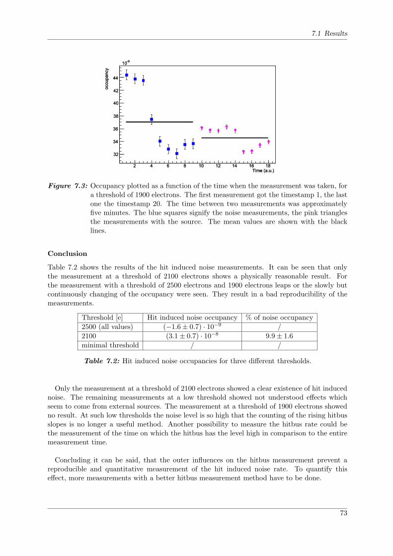
7.1 Results
Time (a.u.)2 4 6 8 10 12 14 16 18
occu
pa
ncy
32
34
36
38
40
42
44
-910
Time (a.u.)2 4 6 8 10 12 14 16 18
occu
pa
ncy
32
34
36
38
40
42
44
-910
Figure 7.3: Occupancy plotted as a function of the time when the measurement was taken, fora threshold of 1900 electrons. The first measurement got the timestamp 1, the lastone the timestamp 20. The time between two measurements was approximatelyfive minutes. The blue squares signify the noise measurements, the pink trianglesthe measurements with the source. The mean values are shown with the blacklines.
Conclusion
Table 7.2 shows the results of the hit induced noise measurements. It can be seen that onlythe measurement at a threshold of 2100 electrons shows a physically reasonable result. Forthe measurement with a threshold of 2500 electrons and 1900 electrons leaps or the slowly butcontinuously changing of the occupancy were seen. They result in a bad reproducibility of themeasurements.
Threshold [e] Hit induced noise occupancy % of noise occupancy
2500 (all values) (−1.6± 0.7) · 10−9 /
2100 (3.1± 0.7) · 10−8 9.9± 1.6
minimal threshold / /
Table 7.2: Hit induced noise occupancies for three different thresholds.
Only the measurement at a threshold of 2100 electrons showed a clear existence of hit inducednoise. The remaining measurements at a low threshold showed not understood effects whichseem to come from external sources. The measurement at a threshold of 1900 electrons showedno result. At such low thresholds the noise level is so high that the counting of the rising hitbusslopes is no longer a useful method. Another possibility to measure the hitbus rate could bethe measurement of the time on which the hitbus has the level high in comparison to the entiremeasurement time.
Concluding it can be said, that the outer influences on the hitbus measurement prevent areproducible and quantitative measurement of the hit induced noise rate. To quantify thiseffect, more measurements with a better hitbus measurement method have to be done.
73

8 Summary and Outlook
For the measurements that are described in this thesis a laser system for charge injection in asemiconductor sensor was built. The adjustment of this laser system was one of the main tasksthat had to be done for the realization of these measurements. The whole system was built to beflexible, the changing of the used laser head or the changing of the devices under test is possiblewithin a few minutes. Two laser heads, with wavelengths of 671 nm and 1060 nm, which are usedto inject charge in different depths into a sensor, are available. For the realization of differentbeamspot diameters one can choose between four different objective lenses. The laser intensitycan be set by an attenuator, and the temperature of the device under test can be controlled,too.During the measurements the system showed a good performance and allowed very precise chargeinjection. In chapter 4 it was shown that it is possible to set injection charges with an accuracyof several ten electrons. The system also allows injecting charges of less than 100 electrons, ormore than 200000 electrons, in silicon. With the 20× object lens it is possible to reach laserbeamspot diameters of about 10µm. With a finer adjustment of the laser system’s componentsit will be possible to reach even smaller beamspot diameters. Furthermore, the re-installation ofthe 50× objective lens will lead to a much smaller beamspot diameter. With these improvementsit will be possible to do spatially resolved measurements within one single pixel.
With the help of this laser system it was possible to examine different module behaviours.The possibility of doing time resolved measurements allowed to disentangle the behaviours of theFE-chip and the sensor by injecting charges at various times. The comparison of an unirradiatedsample with an irradiated one lead to statements about irradiation caused changes of the hitdetection efficiency during a bunchcrossing. These measurements showed, after the irradiationwith the ATLAS lifetime dose, very good FE-chip as well as good sensor performances.The irradiation caused changing of the hit detection probability, and its behaviour at the edgesof a bunchcrossing were shown. Furthermore, an interesting change in the timewalk behaviourwas observed. Additionally, some not understood effects were observed during the measure-ments. It was suggested that some of these effects have their origin in the setting of the chargeinjection time. This was the biggest problem occurring during the measurements, where thebiggest source of errors was the setting of the laser injection time by extending a delay cable.For a better time resolution and a more exact setting of the charge injection time this delaymechanism has to be improved. A possible mechanism, which is able to fulfill such a task, is afrequency generator with two outputs triggered by the same signal. If one of these outputs hasthe possibility to send its signal delayed, the laser injection time can be set very precisely andmechanical defects in the delay line can be excluded.
The hit induced noise measurements by measuring the hitbus rate were not successful. Forfurther investigation on this effect, a completely new method to measure the hitbus, or even thesensor noise itself, has to be invented.
In conclusion, it can be said that as long as the modules are working, the hit detection efficiency
75

8 Summary and Outlook
is good. So even when the ATLAS lifetime dose for the b layer is exceeded (after approximatelyfive years), the modules are supposed to work with a good hit detection probability.
76

Bibliography
[1] D. Griffiths, Einfuhrung in die Elementarteilchenphysik, vol. 1, Akademie Verlag, (1996).
[2] Standard Model of Elementary Particles, website, available online athttp://www.neuroquantology.com/repository/index.php?option=com fireboard&Itemid=54&func=view&catid=40&id=44; visited on March 21th 2011.
[3] K. Nakamura et al, Review of Particle Physics, Jornal of Physics G 37 (2010).
[4] The LEP Higgs Working Group, Search for the Standard Model Higgs Boson at LEP,arXiv:hep-ex/0306033v1.
[5] Supersymetric Particles, website, available online athttp://hasylab.desy.de/images/content/e232/e242/index eng.html; visited on March 29th2011.
[6] Overall View of the LHC Experiment, website, available online athttp://livefromcern.web.cern.ch/livefromcern/antimatter/history/historypictures/LHC-drawing-half.jpg; visited on November 17th2010.
[7] LHC Design Report, CERN-2004-003-V-2 (2007).
[8] M. Lamon, Status of LHC, website, available online athttp://indico.cern.ch/getFile.py/access?contribId=0&resId=1&materialId=slides&confId=113256; visited on April 18th 2011.
[9] J. Grosse-Knetter, Vertex Measurement at Hadron Colider - The ATLAS Pixel Detector,University Bonn (2007).
[10] The Atlas Experiment, website, available online at http://www.atlas.ch; visited onOctober 14th 2010.
[11] The ATLAS Collaboration, The ATLAS Inner Detector commissioning and calibration,arXiv:1004.5293v2 (2008).
[12] B. M. Demirkoz, Construction and Performance of the ATLAS SCT Barrels and CosmicTests, Oxford University (2007).
[13] The ATLAS Muon system, website, available online at http://www.physik.uni-wuerzburg.de/fileadmin/11010700/Teilchenphysik/ATLAS-muon-xy-tdr.jpg; visited onNovember 24th 2010.
[14] The ATLAS Pixel Detector, website, available online athttp://www.atlas.ch/inner detector1.html; visited on Mai 5th 2011.
77

Bibliography
[15] M. George, Implementation of an Electronical Read-Out System for Multi-ModuleLaboratory Tests of the ATLAS Pixel Detector; diploma tesis, Georg-August-UniversitatGottingen (2010).
[16] The ATLAS Pixel Module, website, available online athttp://hep1.physik.uni-bonn.de/atlas pixels.html; visited on Mai 5th 2011.
[17] C. Gemme, Study of indium bumps for the ATLAS pixel detector, Nuclear Instrumentsand Methods in Physics Research 465 (2001).
[18] F. G. Hugging, Der ATLAS Pixel Sensor Der state-of-the-art Pixelsensor furteilchenphysikalische Anwendungen mit extrem hohen Strahlungsfeldern; PHD Thesis.
[19] P. Hettkamp, Messungen zur Charakterisierung der Ladungsmessung vonDEPFET-Matrizen durch Lasereinstrahlung; diploma thesis, University Bonn (2007).
[20] F. Scholz, H. Henneken, P. Kuschnerus, H. Rabus, M. Richter, and G. Ulm, Determinationof the electron-hole pair creation energy for semiconductors from the spectral responsivityof photodiodes, Nuclear Instruments and Methods in Physics Research A 439 (2000).
[21] T. Flick, Studies on the Optical Readout for the ATLAS Pixel Detector; SystematicalStudies on the Functions of the Back of Crate Card and the Timing of the Pixel Detecto;PHD Thesis.
[22] F. Huegging, Der ATLAS Pixel Sensor; PHD Thesis, Universitat Dortmund (2001).
[23] T. Flick, Studies of the Optical Readout for the ATLAS Pixel Detector; PHD Thesis,Universitat Wuppertal (2006).
[24] Neutron fluence, website, available online athttp://rd11.web.cern.ch/RD11/rkb/PH14pp/node123.html; visited on Mai 20th 2011.
[25] O. Krasel, Charge Collection in irradiated Silicon-Sensors; PHD Thesis, UniversityDortmund (2004).
[26] J. Schneider and H. Kruger, S3 Multi IO System, website, available online athttp://icwiki.physik.uni-bonn.de/twiki/pub/System/WebHome/S3 Multi USB V1.0Documentation; visited on Mai 26th 2011.
[27] USBPix - USB based readout system for ATLAS FE-I3 and FE-I4, website, availableonline athttp://icwiki.physik.uni-bonn.de/twiki/bin/view/Systems/UsbPix#Introduction; visitedon Mai 10th 2011.
[28] H. Kruger, Test Systems for ATLAS Pixel Detector Upgrade Activities, University Bonn(2008).
[29] K. Schmieden, Charakterisierung einer neuen Generation von DEPFET-Sensoren mitHilfe eines Lasermesssystems; diploma thesis, University Bonn (2008).
[30] A. R. Shayan, Laser absorption for Si and SiC, website, available online atwww.wmich.edu/mfe/mrc/Amir%20and%20Broga Laser%20Absorbtion%20for%20Si%20and%20SiC 10-24-2008.pdf.
78
Bibliography
[31] D. McMorrow at al., Subbandgap Laser-Induced Single Event Effects: Carrier Generationvia Two-Photon Absorption, IEEE Transactions on nuclear science 49 (2002).
[32] Picosecond Injection Laser (PiLas) - Owner’s Manual Rev. 0.3 Dec. 04, Advanced LaserDiode Systems A.L.S. GmbH (2004).
[33] Private communications with Boris Khoury from ALS.
[34] Sony CCD Black-and-With Video Camera Module - Operating Instructions, SonyCoperation (1999).
[35] Probe Systems PA300IS PA300PS - User Manual M10-123299ß02, Suss MicroTec 2006.
[36] att systems, Manual Control Unit A Series B Series C Series, ATT Systems GmbH 2004.
[37] Manual: Prazisions Temperatursensor CON-TS-NTC, Hygrosens Instruments GmbH2008.
[38] Hamamatsu Si photodiode with preamp S9269, S9270 Datasheet, Hamamatsu PhotonicsK.K. Solid State Division (2004).
[39] F. Kohler, Performance Study of a Diamond Pixel Detector Prototype for Future ATLASUpgrades Using Beam Test Data; diploma teases, University Gottingen (2010).
[40] F. Kinsey at al., The NUDAT/PCNUDAT Program for Nuclear Data, website, availableonline athttp://web.archive.org/web/20040109104128/www2.bnl.gov/CoN/nuc/C/Cd109.shtml;visited on March 7th 2011.
[41] Industrial Radiation Sources - Product information, Eckert & Ziegler Isotope Products2008.
[42] F. K. Kneubuhl and M. F. Sigrist, Laser, vol. 7, Vieweg+Teubner, (2008).
[43] Private communications with Matthias George.
[44] Serie AFG3000 Arbitrarsignal-/Funktionsgeneratror Schnellstart-Benutzerhandbuch,Tektronix 071-1633-04.
[45] T. Lari, Radiation hardness studies of silicon pixel detectors, Nuclear Instruments andMethods in Physics Research A 560 (2005).
[46] J. Rieger, Bachelor’s Thesis: Measurement of Operational Stability of the ATLAS PixelRead-Out Chip at low Threshold, Georg-August-Universitat Gottingen (2010).
79


Acknowledgements
First of all I would like to thank Prof. Dr. Arnulf Quadt, who gave me the possibility to writemy diploma thesis in his working group. It has been a great experience to work in a field ofresearch, where the fundamental coherences in nature are explored.I also want to thank PD. Dr. Jorn Grosse-Knetter for his supports and for a large number ofgreat ideas during the evolution of this work.
Especially I would like to thank Dr. Jens Weingarten, my supervisor during my time in theII physical institute. Without his help and his supervision, this thesis would not have beenpossible. I would like to thank him for the stimulating discussions and for the great help byfixing many problems which occurred during this thesis.
I also want to thank Natascha, who had reviewed this thesis and had supported me duringthe work on this thesis. Last, but not least, I would like to thank the whole HEP working groupof the II physical institute for a great time and a good working atmosphere.
81