Geometric Programming and Its Applications to EDA Problems
135
Geometric Programming and Its Applications to EDA Problems Stephen Boyd Seung Jean Kim S. S. Mohan Boyd, Kim, & Mohan, DATE Tutorial 2005
Transcript of Geometric Programming and Its Applications to EDA Problems

Geometric Programming and
Its Applications to EDA Problems
Stephen Boyd Seung Jean Kim S. S. Mohan
Boyd, Kim, & Mohan, DATE Tutorial 2005

Outline
• Basic approach
• Geometric programming & generalized geometric programming
• Digital circuit design applications
• Analog and RF circuit design applications
• Monomial and posynomial fitting
• Conclusions
Boyd, Kim, & Mohan, DATE Tutorial 2005 1

Basic Approach

Basic approach
1. formulate circuit design problem as geometric program (GP), anoptimization problem with special form
2. solve GP using specialized, tailored method
• this tutorial focuses on step 1 (a.k.a. GP modeling)
• step 2 is technology
Boyd, Kim, & Mohan, DATE Tutorial 2005 2

Why?
• we can solve even large GPs very effectively, using recently developedmethods
• so once we have a GP formulation, we can solve circuit design problemeffectively
we will see that
• GP is especially good at handling a large number of concurrentconstraints
• GP formulation is useful even when it is approximate
Boyd, Kim, & Mohan, DATE Tutorial 2005 3

Trade-offs in optimization
• general trade-off between generality and effectiveness
• generality
– number of problems that can be handled– accuracy of formulation– ease of formulation
• effectiveness
– speed of solution, scale of problems that can be handled– global vs. local solutions– reliability, baby-sitting, starting point
Boyd, Kim, & Mohan, DATE Tutorial 2005 4

Example: least-squares vs. simulated annealing
least-squares
• large problems reliably (globally) solved quickly
• no initial point, no algorithm parameter tuning
• solves very restricted problem form
• with tricks and extensions, basis of vast number of methods that work(control, filtering, regression, . . . )
simulated annealing
• can be applied to any problem (more or less)
• slow, needs tuning, babysitting; not global in practice
• method of choice for some problems you can’t handle any other way
Boyd, Kim, & Mohan, DATE Tutorial 2005 5

Where GP fits in
somewhere in between, closer to least-squares . . .
• like least-squares, large problems can be solved reliably (globally), nostarting point, tuning, . . .
• solves a class of problems broader than least-squares, less general thansimulated annealing
• formulation takes effort, but is fun and has high payoff
Boyd, Kim, & Mohan, DATE Tutorial 2005 6

Geometric Programming &Generalized Geometric Programming

Monomial & posynomial functions
x = (x1, . . . , xn): vector of positive optimization variables
• function g of formg(x) = cxα1
1 xα22 · · ·xαn
n ,
with c > 0, αi ∈ R, is called monomial
• sum of monomials, i.e., function f of form
f(x) =
t∑
k=1
ckxα1k1 x
α2k2 · · ·xαnk
n ,
with ck > 0, αik ∈ R, is called posynomial
Boyd, Kim, & Mohan, DATE Tutorial 2005 7

Examples
with x, y, z variables,
• 0.23, 2z√
x/y, 3x2y−.12z are monomials (hence also posynomials)
• 0.23 + x/y, 2(1 + xy)3, 2x + 3y + 2z are posynomials
• 2x + 3y − 2z, x2 + tanx are neither
Boyd, Kim, & Mohan, DATE Tutorial 2005 8

Generalized posynomials
f is a generalized posynomial if it can be formed using addition,multiplication, positive power, and maximum, starting from posynomials
examples:
• max1 + x1, 2x1 + x0.2
2 x−3.93
•(0.1x1x
−0.53 + x1.7
2 x0.73
)1.5
•(max
1 + x1, 2x1 + x0.2
2 x−3.93
)1.7+ x1.1
2 x3.73
Boyd, Kim, & Mohan, DATE Tutorial 2005 9

Composition rules
• monomials closed under product, division, positive scaling, power,inverse
• posynomials closed under sum, product, positive scaling, division bymonomial, positive integer power
• generalized posynomials closed under sum, product, max, positivescaling, division by monomial, positive power
Boyd, Kim, & Mohan, DATE Tutorial 2005 10

Generalized geometric program (GGP)
minimize f0(x)subject to fi(x) ≤ 1, i = 1, . . . , m
gi(x) = 1, i = 1, . . . , p
fi are generalized posynomials, gi are monomials
• called geometric program (GP) when fi are posynomials
• a highly nonlinear constrained optimization problem
Boyd, Kim, & Mohan, DATE Tutorial 2005 11

GP example
• maximize volume of box with width w, height h, depth d
• subject to limits on wall and floor areas, aspect ratios h/w, d/w
maximize hwdsubject to 2(hw + hd) ≤ Awall, wd ≤ Aflr
α ≤ h/w ≤ β, γ ≤ d/w ≤ δ
in standard GP form:
minimize h−1w−1d−1
subject to (2/Awall)hw + (2/Awall)hd ≤ 1, (1/Aflr)wd ≤ 1αh−1w ≤ 1, (1/β)hw−1 ≤ 1γwd−1 ≤ 1, (1/δ)w−1d ≤ 1
Boyd, Kim, & Mohan, DATE Tutorial 2005 12

GGP example: Floor planning
• choose cell widths, heights
• fixed cell areas
• (1 left of 2) above (3 left of 4)
• aspect ratio constraints
• minimize bounding box area
w1 w2
w3w4
w
h1 h2
h3 h4
h
minimize hwsubject to hiwi = Ai, 1/αmax ≤ hi/wi ≤ αmax,
maxh1, h2 + maxh3, h4 ≤ h,maxw1 + w2, w3 + w4 ≤ w
. . . a GGP
Boyd, Kim, & Mohan, DATE Tutorial 2005 13

Trade-off analysis
(no equality constraints, for simplicity)
• form perturbed version of original GP, with changed righthand sides:
minimize f0(x)subject to fi(x) ≤ ui, i = 1, . . . , m
• ui > 1 (ui < 1) means ith constraint is relaxed (tightened)
• let p(u) be optimal value of perturbed problem
• plot of p vs. u is (globally) optimal trade-off surface (of objectiveagainst constraints)
Boyd, Kim, & Mohan, DATE Tutorial 2005 14

Trade-off curves for maximum volume box example
Afloor
V
Awall = 100Awall = 100
Awall = 1000Awall = 1000
Awall = 10000Awall = 10000
10 102 10310
102
103
104
105
• maximum volume V vs. Aflr, for Awall = 100, 1000, 10000
• h/w, d/w aspect ratio limits 0.5, 2
Boyd, Kim, & Mohan, DATE Tutorial 2005 15

Sensitivity analysis
• optimal sensitivity of ith constraint is
Si =∂p/p
∂ui/ui
∣∣∣∣u=1
• Si predicts fractional change in optimal objective value if ith constraintis (slightly) relaxed or tightened
• very useful in practice; give quantitative measure of how tight a bindingconstraint is
• when we solve a GP we get all optimal sensitivities at no extra cost
Boyd, Kim, & Mohan, DATE Tutorial 2005 16

Example
• minimize circuit delay, subject to power, area constraints (details later)
minimize D(x)subject to P (x) ≤ Pmax, A(x) ≤ Amax
• both constraints tight at optimal x⋆: P (x⋆) = Pmax, A(x⋆) = Amax
• suppose optimal sensitivities are Spwr = −2.1, Sarea = −0.3
• we predict:
– for 1% increase in allowed power, optimal delay decreases 2.1%– for 1% increase in allowed area, optimal delay decreases 0.3%
Boyd, Kim, & Mohan, DATE Tutorial 2005 17

GP and GGP attributes
• after log transform of variables/constraints, they become convexproblems
• can convert GGP to GP, e.g., f(x) + maxg(x), h(x) ≤ 1 becomes
f(x) + t ≤ 1, g(x)/t ≤ 1, h(x)/t ≤ 1
where t is new (dummy) variable
• conversion tricks can be automated
– parser scans problem description, forms GP– efficient GP solver solves GP– solution transformed back (dummy variables eliminated)
Boyd, Kim, & Mohan, DATE Tutorial 2005 18

How GPs are solved
the practical answer: none of your business
more politely: you don’t need to know
it’s technology:
• good algorithms are known
• good software implementations are available
Boyd, Kim, & Mohan, DATE Tutorial 2005 19

How GPs are solved
• work with log of variables: yi = log xi
• take log of monomials/posynomials to get
minimize log f0(ey)
subject to log fi(ey) ≤ 0, i = 1, . . . , m
log gi(ey) = 0, i = 1, . . . , p
• log fi(ey) are (smooth) convex functions
• log gi(ey) are affine functions, i.e., linear plus a constant
• solve (nonlinear) convex optimization problem above usinginterior-point method
Boyd, Kim, & Mohan, DATE Tutorial 2005 20

Current state of the art
• basic interior-point method that exploits sparsity, generic GP structure
• approaching efficiency of linear programming solver
– sparse 1000 vbles, 10000 monomial terms: few seconds– sparse 10000 vbles, 100000 monomial terms: minute– sparse 106 vbles, 107 monomial terms: hour
(these are order-of-magnitude estimates, on simple PC)
Boyd, Kim, & Mohan, DATE Tutorial 2005 21

History
• GP (and term ‘posynomial’) introduced in 1967 by Duffin, Peterson,Zener
• engineering applications from the very beginning
– early applications in chemical, mechanical, power engineering– digital circuit transistor and wire sizing with Elmore delay since 1984
(Fishburn & Dunlap’s TILOS)– analog circuit design since 1997 (Hershenson, Boyd, Lee)– other applications in finance, wireless power control, statistics, . . .
• extremely efficient solution methods since 1994 or so(Nesterov & Nemirovsky)
Boyd, Kim, & Mohan, DATE Tutorial 2005 22

Mixed-integer geometric program
minimize f0(x)subject to fi(x) ≤ 1, i = 1, . . . ,m
gi(x) = 1, i = 1, . . . , pxi ∈ Di, i = 1, . . . , k
• fi are generalized posynomials, gi are monomials
• Di are discrete sets, e.g., 1, 2, 3, 4, . . . or 1, 2, 4, 8 . . .• very hard to solve exactly; all methods make some compromise
(compared to methods for GP)
• heuristic methods attempt to find good approximate solutions quickly,but cannot guarantee optimality
• global methods always find the global solution, but can be extremelyslow
Boyd, Kim, & Mohan, DATE Tutorial 2005 23

Digital Circuit Design Applications

Gate scaling
1
2
3
4
5
6
7
input flip flops output flip flops
in out
clock
combinational logic block
• combinational logic; circuit topology & gate types given
• gate sizes (scale factors xi ≥ 1) to be determined
• scale factors affect total circuit area, power and delay
Boyd, Kim, & Mohan, DATE Tutorial 2005 24

RC gate delay model
PSfrag
Ri
Vdd
C ini
C ini
C inti CL
i
• input & intrinsic capacitances, driving resistance, load capacitance
C ini = C in
i xi, C inti = C int
i xi, Ri = Ri/xi, CLi =
∑
j∈FO(i)
C inj
Boyd, Kim, & Mohan, DATE Tutorial 2005 25

RC gate model
• RC gate delay:
Di = 0.69Ri(CLi + C int
i ) = 0.69
RiCini + (Ri/xi)
∑
j∈FO(i)
C inj xj
• Di are posynomials (of scale factors)
Boyd, Kim, & Mohan, DATE Tutorial 2005 26

Path and circuit delay
1
2
3
4
5
6
7
• delay of a path: sum of delays of gates on path. . . posynomial
• circuit delay: maximum delay over all paths. . . generalized posynomial
Boyd, Kim, & Mohan, DATE Tutorial 2005 27

Area & power
• total circuit area: A = x1A1 + · · · + xnAn
• total power is P = Pdyn + Pstat
– dynamic power Pdyn =
n∑
i=1
fi(CLi + C int
i )V 2dd
fi is gate switching frequency
– static power Pstat =
n∑
i=1
xiIleaki Vdd
I leaki is leakage current (average over input states) of unit scaled gate
• A and P are linear functions of x, with positive coefficients, henceposynomials
Boyd, Kim, & Mohan, DATE Tutorial 2005 28

Basic gate scaling problem
minimize Dsubject to P ≤ Pmax, A ≤ Amax
1 ≤ xi, i = 1, . . . , n
. . . a GGP
extensions/variations:
• minimize area, power, or some combination
• maximize clock frequency subject to area, power limits
• add other constraints
• optimal trade-off of area, power, delay
Boyd, Kim, & Mohan, DATE Tutorial 2005 29

Clock frequency maximization
• fclk is variable
• timing requirement: D ≤ 0.8/fclk
(20% margin for flip-flop delay, setup time, clock skew . . . )
• P is posynomial of scalings and fclk, assuming fi scale with fclk
maximize fclk
subject to P ≤ Pmax, A ≤ Amax, (1/0.8)Dfclk ≤ 1,1 ≤ xi, i = 1, . . . , n
. . . a GGP
Boyd, Kim, & Mohan, DATE Tutorial 2005 30

Example: 32-bit Ladner-Fisher adder
• 451 gates (scale factors), 5 gate types, 64 inputs, 32 outputs
• logical effort gate delay model parameters:
gate type C in C int R A I leak
INV 3 3 0.48 3 0.006NAND2 4 6 0.48 8 0.007NOR2 5 6 0.48 10 0.009AOI21 6 7 0.48 17 0.003OAI21 6 7 0.48 16 0.003
• time unit is τ , delay of min-size inverter (0.69 · 0.48 · 3 = 1)
• area (total width) unit is width of NMOS in min-size inverter
Boyd, Kim, & Mohan, DATE Tutorial 2005 31

Example: 32-bit Ladner-Fisher adder
• typical optimization time: few seconds on PC
D
Am
ax
45 703000
16000
Boyd, Kim, & Mohan, DATE Tutorial 2005 32

32-bit Ladner-Fisher adder with discrete scale factors
• add constraints xi ∈ 1, 2, 4, 8, 16, . . .• simple rounding of optimal continuous scalings
D
Am
ax
45 703000
16000 simple roundingoptimal continuous
Boyd, Kim, & Mohan, DATE Tutorial 2005 33

Sparse GP gate scaling problem
minimize Dsubject to Tj ≤ D for j an output gate
Tj + Di ≤ Ti for j ∈ FI(i)P ≤ Pmax, A ≤ Amax
1 ≤ xi, i = 1, . . . , n
• Ti are upper bounds on signal arrival times
• extremely sparse GP; can be solved very efficiently
Boyd, Kim, & Mohan, DATE Tutorial 2005 34

Better (generalized posynomial) models
can greatly improve model, while retaining GP compatibility(hence efficient global solution)
• area, delay, power can be any generalized posynomials of scale factors,e.g.,
Di = ai + bi(CLi )1.05x−0.9
i , Pi = ci + di(CLi )1.2 + eix
1.1i
• these can be found by more refined analysis, or fitting generalizedposynomials to simulation/characterization data
Boyd, Kim, & Mohan, DATE Tutorial 2005 35

Distinguishing gate transitions
• can distinguish rising and falling transitions, with different delay, energy,C in, for each gate input/transition
• (bounds on) signal arrival times can be propagated through recursions,e.g.,
T ri = max
j∈FI(i)
T r
j + Drrji, T f
j + Dfrji
, T f
i = maxj∈FI(i)
T r
j + Drfji, T f
j + Dffji
• gate scaling problem more complex, but still a GGP(hence can be efficiently solved)
Boyd, Kim, & Mohan, DATE Tutorial 2005 36

Modeling signal slopes
• associate (worst-case) output signal transition time τ with each gate
• model delay, energy, input capacitance as (generalized posynomial)functions of scale factor, load capacitance, input transition time
• propagate output transition time using (generalized posynomial)function of scale factor, load capacitance, input transition time
• common model:
Di = aiCLi /xi +κiτ
ini , Ei = bi(C
Li + cixi)+λixiτ
ini , τi = νiDi
• gate scaling problem still a GGP
Boyd, Kim, & Mohan, DATE Tutorial 2005 37

Design with a standard library
• circuit topology is fixed; choose size for each gate from discrete library
• a combinatorial optimization problem, difficult to solve exactly
• GP approach
– for each gate type in library, fit given library data to findGP-compatible models of delay, power, . . .
– size with continuous fitted models, using GP
– snap continuous scale factors back to standard library
Boyd, Kim, & Mohan, DATE Tutorial 2005 38

Robust design over corners
• have K corners or scenarios, e.g., combinations of
– process parameters (channel length, oxide thickness, . . . )– environmental parameters (supply voltage, temperature, . . . )
• for each corner have (slightly) different models for delay, power, . . .
• robust design finds gate scalings that work well for all corners
Boyd, Kim, & Mohan, DATE Tutorial 2005 39

Robust design over corners
• basic (worst-case) robust design over corners:
minimize Dwc = maxD(1), . . . , D(K)subject to P (1)(x) ≤ Pmax, . . . , P (K)(x) ≤ Pmax
A ≤ Amax
1 ≤ xi, i = 1, . . . , n
• many variations, e.g., minimize average delay over corners,
Davg = (1/K)(D(1) + · · · + D(K)
)
• results in (very large, but sparse) GGP
Boyd, Kim, & Mohan, DATE Tutorial 2005 40

Multiple-scenario design
• have K scenarios or operating modes, with K models for P , D, . . .
• scenarios are combinations of
– supply & threshold voltages– clock frequency– specifications & constraints
• like corner-based robust design, but scenarios are intentional
• find one set of gate scalings that work well in all scenarios
Boyd, Kim, & Mohan, DATE Tutorial 2005 41

Example
• find single set of gate scalings to support both high performance modeand low power mode
– in high performance mode: P fast ≤ P fast, Dfast ≤ Dfast
– in low power mode: P slow ≤ P slow, Dslow ≤ Dslow
minimize Asubject to P slow ≤ P slow, Dslow ≤ Dslow
P fast ≤ P fast, Dfast ≤ Dfast
1 ≤ xi, i = 1, . . . , n
. . . a GGP
Boyd, Kim, & Mohan, DATE Tutorial 2005 42

Statistical parameter variation
• circuit peformance depends on random device and process parameters
• hence, performance measures like P , D are random variables P, D
• delay D is max of many random variables; often skewed to right
• distributions of P, D depend on gate scalings xi
45 53circuit delay
freq
uen
cy
• related to (parametric) yield, DFM, DFY . . .
Boyd, Kim, & Mohan, DATE Tutorial 2005 43

Statistical design
• measure random performance measures by 95% quantile (say)
minimize Q.95(D)subject to Q.95(P) ≤ Pmax, A ≤ Amax
1 ≤ xi, i = 1, . . . , n
• extremely difficult stochastic optimization problem; almost noanalytic/exact results
• but, (GP-compatible) heuristic method works well
Boyd, Kim, & Mohan, DATE Tutorial 2005 44

Statistical model
• for simplicity consider Vth variation only
• Pelgrom’s model: σVth= σVth
x−1/2
• alpha-power law model: D ∝ Vdd/(Vdd − Vth)α, with α ≈ 1.3
• for small variation in Vth,
σD ≈∣∣∣∣∂D
∂Vth
∣∣∣∣ σVth= α(Vdd − Vth)
−1σVthx−0.5D
• σD is posynomial
• get similar (posynomial) models for σD with more complex gate delaystatistical models
Boyd, Kim, & Mohan, DATE Tutorial 2005 45

Heuristic for statistical design
• assume generalized posynomial models for gate delay mean Di(x) andvariance σi(x)2
• optimize using surrogate gate delays
Di(x) = Di(x) + κiσi(x)
κiσi(x) are margins on gate delays (κi is typically 2 or 3)
• verify statistical performance via Monte Carlo analysis(can update κi’s and repeat)
Boyd, Kim, & Mohan, DATE Tutorial 2005 46

Heuristic for statistical design
heuristic statistical design
• often far superior to design obtained ignoring statistical variation
• not very sensitive to details of process variation statistics (distributionshape, correlations, . . . )
• below: 32-bit Ladner-Fisher adder, Pelgrom variance model
45 53circuit delay
freq
uen
cy
statistical design
nominal optimal design
Boyd, Kim, & Mohan, DATE Tutorial 2005 47

Path delay mean/std. dev. scatter plots
mean path delay
mean path delay
pat
hdel
ayst
d.dev
.pat
hdel
ayst
d.dev
.
10
10
50
50
0
0
3
3nominal optimal design
statistical design
Boyd, Kim, & Mohan, DATE Tutorial 2005 48

Joint size and supply/threshold voltage optimization
• goal: jointly optimize gate size, supply and threshold voltages via GGP
• need to: model delay, power as generalized posynomial functions ofgate size, supply and threshold voltages
Boyd, Kim, & Mohan, DATE Tutorial 2005 49

Generalized posynomial delay model
• alpha-power law model predicts variation in gate delay with Vdd, Vth:
Di =Vdd,i
(Vdd,i − Vth,i)αDi(x)
Di is generalized posynomial gate delay model, function of scalings x
• generalized posynomial approximation
Di = V 1−αdd,i (1 + Vth,i/Vdd,i + · · · + (Vth,i/Vdd,i)
5)αDi(x)
error under 1% for Vdd,i ≥ 2Vth,i, 1.3 ≤ α ≤ 2
Boyd, Kim, & Mohan, DATE Tutorial 2005 50

Generalized posynomial power model
• gate dynamic power: Pdyn =n∑
i=1
fi(CLi + C int
i )V 2dd,i
• simple static power model:
Pstat =
n∑
i=1
xiIleaki Vdd,i, I leak
i ∝ e−(Vth,i−γVdd,i)/V0
γ, V0 are (process) constants
• Pstat (by itself) cannot be approximated well by a generalizedposynomial over large range of Vdd, Vth
• but, total power P = Pdyn + Pstat can be approximated well by ageneralized posynomial
Boyd, Kim, & Mohan, DATE Tutorial 2005 51

Generalized posynomial power model example
total power P = V 2dd + 30Vdde
−(Vth−0.06Vdd)/0.039 (up to scaling)
VddVth
P
1
2
0.2
0.4
1
12
VddVth 1
2
0.2
0.4
1
12
|P−
b P|
• generalized posynomial approximationP = V 2
dd + 0.06Vdd(1 + 0.0031Vdd)500(Vth/0.039)−6.16
• error under 3% (well under accuracy of model!)
Boyd, Kim, & Mohan, DATE Tutorial 2005 52

Joint optimization of gate sizes, Vdd, & Vth
basic problem, with variables: xi, Vth,i, Vdd,i
minimize Dsubject to P ≤ Pmax, A ≤ Amax
V minth ≤ Vth,i ≤ V max
th , i = 1, . . . , nV min
dd ≤ Vdd,i ≤ V maxdd , i = 1, . . . , n
other constraints . . .
(. . . a GGP)
discrete allowed Vdd, Vth values yields MIGP
Boyd, Kim, & Mohan, DATE Tutorial 2005 53

Extensions/variations
• clustering, with single Vdd, Vth per cluster:
Vdd,i = Vdd,j, Vth,i = Vth,j for i, j in same cluster
. . . monomial (equality) constraints
• clustered voltage scaling (CVS): low Vdd cells cannot drive high Vdd cells
Vdd,j ≤ Vdd,i for j ∈ FO(i)
. . . monomial (inequality) constraints
• multimode design: choose single set of gate scalings, different V(k)dd ,
V(k)th for each scenario k = 1, . . . ,K
related to dynamic voltage scaling, adaptive bulk biasing, . . .
Boyd, Kim, & Mohan, DATE Tutorial 2005 54

Joint optimization examples
• Ladner-Fisher adder
• variables: gate scalings xi, supply voltages Vdd,i, threshold voltages Vth,i
• four delay-power trade-off curves:
– fixed Vdd,i = 1.0, fixed Vth,i = 0.3
– fixed Vdd,i = 1.0, variable Vth,i ∈ 0.2, 0.3, 0.4– CVS with Vdd,i ∈ 0.6, 1.0, Vth,i ∈ 0.2, 0.3, 0.4– variable continuous Vdd, Vth, 0.6 ≤ Vdd,i ≤ 1.0, 0.2 ≤ Vth,i ≤ 0.4
(not practical, but serves as lower bound)
Boyd, Kim, & Mohan, DATE Tutorial 2005 55

Trade-off curve analysis
Dmax
P
37.5 750
30
lower bound
CVS
fixed Vdd, variable Vth
fixed Vdd, Vth
Boyd, Kim, & Mohan, DATE Tutorial 2005 56

Design with multiple threshold voltages
Dmax
%of
gate
s
35 700%
100%
Vth = 0.4
Vth = 0.3
Vth = 0.2
Boyd, Kim, & Mohan, DATE Tutorial 2005 57

Clustered voltage scaling
%of
gate
s
37.5 750%
100% Vdd = 0.6
Vdd = 1.0
Boyd, Kim, & Mohan, DATE Tutorial 2005 58

Wire and device sizing
RC tree:
R1
R2 R3
R4
R5
R6
C1
C2 C3
C4 C6
C5
• Ris and Cis are generalized posynomials of some underlying variables x
Boyd, Kim, & Mohan, DATE Tutorial 2005 59

Elmore delay
• Elmore delay at node i:
Di =
∫ ∞
0
vi(t) dt
area under voltage curve, when voltages are initialized as vi(0) = 1
t
1 Di
• Elmore delay of RC tree is D = maxD1, . . . , DN
Boyd, Kim, & Mohan, DATE Tutorial 2005 60

Elmore delay expression
• analytic expression for Elmore delay Di
Di =∑
j∈P(i)
RiCtoti
• P(i) is path from root to node i
• Ctoti is the total capacitance downstream from node i (including Ci)
• Di is posynomial of x
• D is generalized posynomial of x
Boyd, Kim, & Mohan, DATE Tutorial 2005 61

RC tree optimization
• minimize RC tree delay subject to (generalized posynomial) constraints
minimize Dsubject to fi(x) ≤ 0, i = 1, . . . , m
. . . a GGP
• sparse formulation:
minimize ssubject to s ≥ Di, i = 1, . . . , n
Ctotj ≥
∑i∈Child(j) Ctot
i + Cj, i = 1, . . . , n
Di ≥ DPar(k) + RiCtoti , i = 1, . . . , n
fi(x) ≤ 0, i = 1, . . . ,m
Boyd, Kim, & Mohan, DATE Tutorial 2005 62

Wire sizing
• choose wire segment widths wi, . . . , wN in an interconnect network
• optimize delay, area
1
2 3
4 5
C1
C2 C3
C4 C5vin
Rs
Boyd, Kim, & Mohan, DATE Tutorial 2005 63

π model for wire segment
wi
li
Ci Ci
Ri
• wire resistance and capacitances
Ri = αiliwi
, Ci = βiliwi + γili,
• with π model, interconnect network becomes RC tree, with Ris and Cisposynomial functions of wire segment widths wi
Boyd, Kim, & Mohan, DATE Tutorial 2005 64

Wire sizing via GP
minimize Dsubject to wmin
i ≤ wi ≤ wmaxi , i = 1, . . . , N
l1w1 + · · · + lNwN ≤ Amax
. . . a GGP
• can easily optimize interconnect network with 10000 wires, using sparseGP formulation
• can use more accurate generalized posynomial models of Ri, Ci
Boyd, Kim, & Mohan, DATE Tutorial 2005 65

Device sizing
• devices (and wire segments) are sized individually
• replace each device with switch-level RC model
• each transition is associated with RC tree
• use Elmore delay to measure delay of transition
• . . . problem is GGP
Boyd, Kim, & Mohan, DATE Tutorial 2005 66

Switch-level RC device model
G
S
D
B
G
G
D
D
S
S
B
B
NMOS
PMOS
Rsd
Cgb
Cgd
Cgs
Cdb
Csb
• crude linear approximation of device, for delay and power optimization
• R, all Cs are generalized posynomials of device width
• we’ll ignore Cgd (but can be incorporated via Miller effect . . . )
Boyd, Kim, & Mohan, DATE Tutorial 2005 67

Example: 2-input NAND
A
B
M1 M2
M3
M4
X
CL
Vdd
Rsd1 Rsd2
Rsd3
Rsd4
C1
C2
C3
C4
B A
A
B
Cdb3
Csb3 + Cdb4
Cdb1 Cdb2A
B
X
CL
Vdd
Vdd
C1 = Cgb2+Cgs2, C2 = Cgb3+Cgs3, C3 = Cgb1+Cgs1, C4 = Cgb4+Cgs4
Boyd, Kim, & Mohan, DATE Tutorial 2005 68

Example transition
• transition: B falls from Vdd to zero; A remains at Vdd
• associated RC tree:
Rsd1
Rsd3C1
C2
CL
Vdd
C1 = Cdb1 + Cdb2 + Cdb3, C2 = Csb3 + Cdb4
• Elmore delay: D = Rsd1(CL + C1 + C2)
• energy lost: E = (CL + C1 + C2)V2dd/2
Boyd, Kim, & Mohan, DATE Tutorial 2005 69

Analog and RF Circuit Design Applications

Large signal MOS model
PMOSNMOS
D
D
G G
S
S
II
• gate overdrive voltage Vgov = Vgs − Vth
• saturation condition: Vds ≥ Vdsat = Vgov (Vdsat is minimumdrain-source voltage for device to operate in saturation)
• square-law model I = 0.5µCox(W/L)V 2gov
• GP model variables: I, L, W
• Vgov = (µCox/2)−1/2I1/2L1/2W−1/2 is monomial
• Vgs = Vgov + Vth is posynomial
Boyd, Kim, & Mohan, DATE Tutorial 2005 70
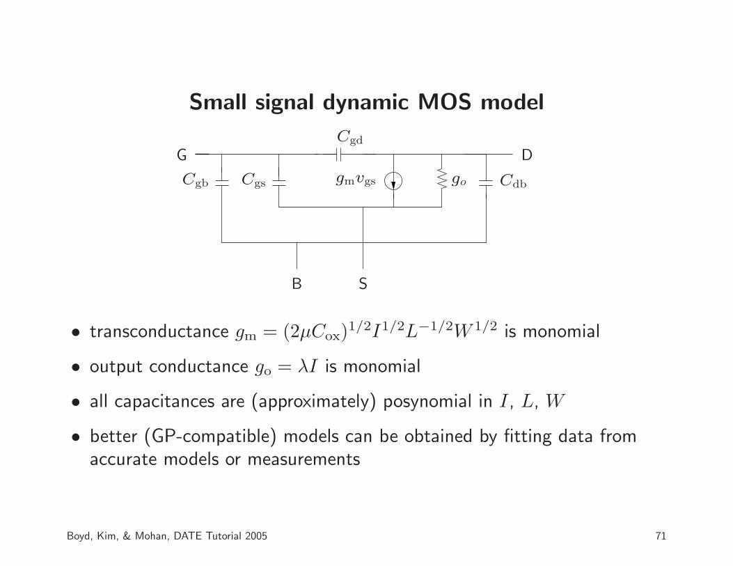
Small signal dynamic MOS model
PSfrag
Cgb Cgs gmvgs go Cdb
Cgd
B S
DG
• transconductance gm = (2µCox)1/2I1/2L−1/2W 1/2 is monomial
• output conductance go = λI is monomial
• all capacitances are (approximately) posynomial in I, L, W
• better (GP-compatible) models can be obtained by fitting data fromaccurate models or measurements
Boyd, Kim, & Mohan, DATE Tutorial 2005 71

Example: monomial gm model
• monomial model of gm for I/O NMOS device in a 0.13µm technology
• 11000 data points (from BSIM3) over ranges
– 0.3µm ≤ L ≤ 3µm, 2µm ≤ W ≤ 20µm– 0.7V ≤ Vgs ≤ 1.7V, Vdsat ≤ Vds ≤ 1.5Vgs
• Vds appears in data set, but not in gm model
• monomial fit (using simple log-regression, SI units):
gm = 0.0278I0.4798L−0.511W 0.5632
Boyd, Kim, & Mohan, DATE Tutorial 2005 72

Example: monomial gm model
• fitting (relative) error cumulative distribution plot:
fitting error
frac
tion
ofdat
apoi
nts
0% 5% 10%0%
100%
• for 90% of points, fit is better than 4%
Boyd, Kim, & Mohan, DATE Tutorial 2005 73

Single transistor common source amplifier
• variables: I, L, W , R
• saturation: Vdsat + IR ≤ Vdd
• gain G = gm/(1/R + go)
• power P = VddI
• (unity gain) bandwidth B = gm/CL
• design problem:
minimize Psubject to B ≥ Bmin, G ≥ Gmin
saturation
CL
R
Vdd
in
out
Boyd, Kim, & Mohan, DATE Tutorial 2005 74

Common source amplifier design via GP
• rewrite as
minimize Psubject to B−1 ≤ 1/Bmin, G−1 ≤ 1/Gmin
Vdsat + IR ≤ Vdd
• . . . a GP, since P and B are monomials, and
G−1 =1/R + go
gm
is posynomial
• this is a simple problem; don’t need GP sledgehammer . . .
Boyd, Kim, & Mohan, DATE Tutorial 2005 75

Current mirror opamp
M1
M3
M5
M6
M7
M2
M4
M8
M9
M10
CL
Iref
Vdd
in+in−
out
• M1,M2 and M3,M4 matched pairs
• four current mirrors: M8,M5; M10,M7; M9,M3; M4, M6
Boyd, Kim, & Mohan, DATE Tutorial 2005 76

Design problem
minimize Psubject to B ≥ Bmin, G ≥ Gmin, A ≤ Amax
other constraints . . .
• objective & specifications:
– P is power dissipation– B is unity gain bandwidth– G is DC gain– A is (active) area
• design variables: L1, . . . , L10, W1, . . . ,W10
• given: Vdd, CL, Iref, common-mode voltage Vcm
• we’ll formulate as GP
Boyd, Kim, & Mohan, DATE Tutorial 2005 77

Power, bandwidth, gain, & area
• power: P = Vdd(I8 + I5 + I7 + I10) . . . posynomial
• bandwidth: B = gm,2gm,6/(gm,4CL) . . . monomial
• area: A = W1L1 + · · · + W10L10 . . . posynomial
• gain: G =gm,2gm,6
gm,4(go,6 + go,7)
. . . G−1 is posynomial, so G ≥ Gmin can be written as G−1 ≤ 1/Gmin
Boyd, Kim, & Mohan, DATE Tutorial 2005 78

Dimension, matching, and current constraints
• limits on device sizes: Lmin ≤ Li ≤ Lmax, Wmin ≤ Wi, i = 1, . . . , 10
• differential symmetry constraints (M1, M2 and M3, M4 matched):
W1 = W2, L1 = L2, I1 = I2,W3 = W4, L3 = L4, I3 = I4,
• length & gate overdrive voltage matched for current mirror pairs:
L5 = L8, L10 = L7, L3 = L9, L4 = L6
Vgov,5 = Vgov,8, Vgov,10 = Vgov,7, Vgov,3 = Vgov,9, Vgov,4 = Vgov,6
• current relations:
I1 = I3 = I5/2, I8 = Iref, I6 = I7, I9 = I10
Boyd, Kim, & Mohan, DATE Tutorial 2005 79

Saturation constraints
• diode connected devices (M3,M4,M8, M10) automatically in saturation
• others must have Vds ≥ Vdsat:
– M7: Vdsat,7 ≤ Vcm
– M6: Vdsat,6 + Vcm ≤ Vdd
– M9: Vdsat,9 + Vgs,10 ≤ Vdd
– M5: Vds,5 + Vgs,1 ≤ Vcm
– M1 & M2: Vcm + Vgs,3 ≤ Vdd + Vth
• . . . all are posynomial inequalities
Boyd, Kim, & Mohan, DATE Tutorial 2005 80

Node capacitances and non-dominant poles
• capacitances at nodes are posynomials, e.g.,
Cout = Cgd,6 + Cdb,6 + Cgd,7 + Cdb,7 + CL
• non-dominant time constants are posynomials:
τ1 =Cd1
gm,3, τ2 =
Cd2
gm,4, τ9 =
Cd9
gm,10
(Cd1, Cd2, Cd9 are node capacitances at drains of M1,M2,M9)
• to limit effect of non-dominant poles, make sum smaller than dominanttime constant:
τ1 + τ2 + τ9 ≤ τdom = CL/gm
. . . a posynomial constraint
Boyd, Kim, & Mohan, DATE Tutorial 2005 81

Power versus bandwidth trade-off
10 6010
−1
100
101
Gmin = 10
Gmin = 20
Gmin = 30
Bmin (MHz)
P(m
W)
Boyd, Kim, & Mohan, DATE Tutorial 2005 82

Joint electrical/physical design
• each device has a (physical) cell width w and height h for floor planning
• devices are folded into multiple fingers
• (approximate) posynomial or monomial relations link electrical variables(I, L, W ) and physical variables (w, h), e.g.,
– cell area is at least 4× active area: wh ≥ 4WL– cell aspect ratio limited to 5:1: 1/5 ≤ w/h ≤ 5
W/6
L
w
h
Boyd, Kim, & Mohan, DATE Tutorial 2005 83

Slicing tree layout scheme
• vertical and horizontal slices fix relative placement of device cells
• leaves are device cells; root is bounding box
v
h h
M1
vM4 M5
M2 M3
M1
M4
M2 M3
M5
wbbox
hbbox
Boyd, Kim, & Mohan, DATE Tutorial 2005 84

Slicing tree constraints
• introduce width, height for each node in slicing tree
• for each vertical slice with parent a and children b, c add constraints
wa = wb + wc, ha = maxhb, hc
• for each horizontal slice with parent a and children b, c add constraints
wa = maxwb, wc, ha = hb + hc
• shows width and height of bounding box and each node is generalizedposynomial of device cell widths, heights
• resulting GP formulation is very sparse
Boyd, Kim, & Mohan, DATE Tutorial 2005 85

Joint electrical/physical design via GP
• form one GP that includes
– electrical variables, constraints (Ii, Li, Wi, gm,i . . .)– physical variables, constraints (wi, hi, w
bbox, hbbox, . . .)– coupling constraints (wihi ≥ 4WiLi, . . . )
• solve it all together
• extensions: can add
– parasitic estimates– more accurate expressions for device cell dimensions– channels for routing
Boyd, Kim, & Mohan, DATE Tutorial 2005 86

Optimal filter implementation
simple Gm-C two-pole lowpass filter
g1g2
C1 C2
inputoutput
transfer function is
H(s) =1
1 + t1s + t1t2s2, t1 = C1/g1, t2 = C2/g2
gi is amplifier transconductance
Boyd, Kim, & Mohan, DATE Tutorial 2005 87

Noise analysis
• Ni is input referred (white) amplifier input-referred voltage density
• spectral density of output noise is
N(ω)2 =N2
1 + ω2N22
(1 − t1t2ω2)2 + t21ω2
• root-mean-square output noise voltage is
M =
(∫ ∞
0
N(ω)2 dω
)1/2
=(αN2
1 + βN22
)1/2
Boyd, Kim, & Mohan, DATE Tutorial 2005 88

Amplifier and capacitor implementation models
• each amplifier has private variables u (e.g., device lengths & widths)and constraints
• transconductance g is monomial in u; area Aamp, power P ,input-referred noise density N are posynomial in u
• each capacitor has private variables v (e.g., physical dimensions) andconstraints
• capacitance C is monomial in v; area Acap is posynomial
• design variables are u1, u2, v1, v2
Boyd, Kim, & Mohan, DATE Tutorial 2005 89

Optimal filter implementation problem
• filter is Butterworth with frequency ωc:
t1 =√
2/ωc, t2 = (1/√
2)/ωc
• minimize total power of implementation, subject to area, output noiselimits:
minimize P (u1) + P (u2)
subject to t1 =√
2/ωc, t2 = (1/√
2)/ωc
Aamp(u1) + Aamp(u2) + Acap(v1) + Acap(v2) ≤ Amax
M = (ωc/4√
2)(N21 + 2N2
2 )1/2 ≤ Mmax
• a GGP in the variables u1, u2, v1, v2
Boyd, Kim, & Mohan, DATE Tutorial 2005 90

Example
• Butterworth filter with ωc = 108rad/s
• private variables in amplifiers: (equivalent) L, W
• amplifier model:
Aamp = WL, P = 2.5·10−4W/L,
g = 4·10−5W/L, N =√
7.5·10−16L/W
(based on simple model with Vdd = 2.5, Vgov = 0.2)
• private variable in capacitors is area Acap; C = 10−4Acap
• Amax = 4·10−6
Boyd, Kim, & Mohan, DATE Tutorial 2005 91

Power versus noise trade-off
pow
erP
(mW
)
max noise Mmax (µV RMS)
10 100
0.1
1
10
Boyd, Kim, & Mohan, DATE Tutorial 2005 92

Spiral inductor/differential resonator optimization
planar loop
inductor−v/2 +v/2
RL
CL
• loop inductor connected to (given) RL and CL
• differential (floating) mode operation
• inductor designed to resonate at operating frequency f
Boyd, Kim, & Mohan, DATE Tutorial 2005 93

Design problem: differential resonator
maximize RT
subject to QT ≥ QminT , A ≤ Amax
other constraints . . .
• objective & specifications:
– RT is tank impedance (which is real at operating frequency f)– QT is tank quality factor– A is area of loop inductor
• design variables: dimensions of loop inductor
• load resistance RL, load capacitance CL, frequency f given
• we’ll formulate as GP
Boyd, Kim, & Mohan, DATE Tutorial 2005 94

Loop inductor
W
D
• (centerline) diameter D
• width W
• outer diameter is D + W ; area is A = (D + W )2
Boyd, Kim, & Mohan, DATE Tutorial 2005 95

Lumped model for loop inductor
L R
C
−v/2 +v/2
• lumped model for operation in differential mode
• impact of substrate capacitance, loss included in R and C
Boyd, Kim, & Mohan, DATE Tutorial 2005 96

Example
• frequency range 2GHz ≤ f ≤ 6GHz
• metal layer thickness 2µm, resistivity 5·10−8Ωm
• metal-substrate capacitance density 5·10−6Fm2
• width, diameter constraints:
150µm ≤ D ≤ 600µm, 4µm ≤ W ≤ 30µm, 10 ≤ D/W ≤ 100
Boyd, Kim, & Mohan, DATE Tutorial 2005 97

GP models for L, R and C
• can get exact values via EM simulation
• inductance (monomial)
L = 2.1·10−6D1.28W−0.25f−0.01
• resistance (posynomial)
R = 0.1DW−1+3·10−6DW−0.84f0.5+5·10−9DW−0.76f0.75+0.02DWf
• capacitance (posynomial):
C = 5·10−6DW + 1·10−11D
Boyd, Kim, & Mohan, DATE Tutorial 2005 98

Resonance constraint
L R
C
RL
CL
−v/2 +v/2
• resonance condition: 4π2f2LCT = 1 (CT = C + CL)
• to handle in GP:
– impose posynomial constraint C + CL ≤ CT
– add extra capacitance (after design) Cextra = CT − C − CL if needed
Boyd, Kim, & Mohan, DATE Tutorial 2005 99

Tank conductance and quality factor
L R
C
RL
CL
−v/2 +v/2
• tank conductance: GT =1
RT=
R
4π2f2L2+
1
RL. . . posynomial
• inverse of tank quality factor:1
QT=
R
2πfL+
2πfL
RL. . . posynomial
Boyd, Kim, & Mohan, DATE Tutorial 2005 100

Reso
nance
impedance
vers
us
area
trade-o
ff
RT(Ω)
Am
ax
(mm
2)
100
300
500 0.0
50.1
50.
25CL
=0.
6pF
CL
=0.
8pF
CL
=1.
0pF
Boy
d,K
im,&
Moh
an,D
AT
ETuto
rial
2005
101

LC oscillator
loopinductor
−v/2 +v/2
Vdd
Ibias
CL CL
...
VcCv Cv
2B−1Csw
Csw
• loop inductor
• varactors for fine tuning
• binary weighted switchingcapacitors for coarse tuning
• cross coupled NMOStransistors
• tail current source
Boyd, Kim, & Mohan, DATE Tutorial 2005 102

LC oscillator design problem
minimize Psubject to N ≤ Nmax, A ≤ Amax, l ≥ lmin
other constraints . . .
• objective & specifications:
– P is power consumption– N is phase noise– A is area of loop inductor– l is loop gain
• given: load capacitance CL, center frequency f , normalized tuningrange T
• we’ll formulate as GP
Boyd, Kim, & Mohan, DATE Tutorial 2005 103

Design variables
loopinductor
−v/2 +v/2
Vdd
Ibias
CL CL
...
VcCv Cv
2B−1Csw
Csw
• loop inductor dimensions D, W
• size of varactor Vc
• size of switching capacitors Csw
• width, length of transistorsWnmos, Lnmos
• bias current Ibias
Boyd, Kim, & Mohan, DATE Tutorial 2005 104

Current source, switched capacitor, and varactor models
• Ibias is bias current, with minimum operating voltage Vbias
• binary weighted capacitors
– B is number of bits for switching capacitors– Csw is LSB switching capacitance; 2B−1Csw is MSB switching
capacitance
• varactor
– Cv is minimum varactor capacitance; KvCv is maximum(Kv is process constant)
– varactor range covers 2 LSB: 2Csw ≤ 0.5(Kv − 1)Cv
Boyd, Kim, & Mohan, DATE Tutorial 2005 105

Tank capacitance
• tank capacitance is sum of Cfix and Ctune
• fixed capacitance is sum of loop, load and transistor capacitances:
Cfix = C + 0.5 (CL + Cgs + 4Cgd + Cdb)
• tunable capacitance is sum of switching and varactor capacitances:
– Ctune for maximum frequency: Ctune = 0.5Cv
– Ctune for minimum frequency: Ctune = 2BCsw + 0.5KvCv
Boyd, Kim, & Mohan, DATE Tutorial 2005 106

Resonance frequency & tuning
• capacitance constraint at maximum frequency: Cfix + 0.5Cv ≤ Cf,max
• maximum frequency: (2πf(1 + T ))2LCf,max = 1
• capacitance at center frequency: (2πf)2LCf,c = 1
• tuning range constraint:
4T
(1 − T 2)2Cf,c ≤ Csw
(2B + 2
)
Boyd, Kim, & Mohan, DATE Tutorial 2005 107

Power & area
• power: P = VddIbias
• area: A = (D + W )2 + 2WnmosLnmos
(can add area of switched capacitors, varactor)
Boyd, Kim, & Mohan, DATE Tutorial 2005 108

Tank conductance & voltage swing
• tank conductance is posynomial: GT =R
4π2f2L2+ 0.5go
• differential voltage amplitude: Vosc + 2Vbias ≤ 2Vdd, VoscGT ≤ Ibias
Boyd, Kim, & Mohan, DATE Tutorial 2005 109

Phase noise
• thermal current noise power density of loop: i2n,L =4kTR
4π2f2L2
• thermal current noise power density of transistor: i2nmos = 4kTγgm
• phase noise in the 1/f2 region:
N =1
16π2f2offC2
TV 2osc
(i2n,L + 0.5i2nmos
)
• . . . can add other noise terms
Boyd, Kim, & Mohan, DATE Tutorial 2005 110

Loop gain and start-up
• inverse of loop gain is posynomial: 1/l = (go + 2G)/gm
• minimum loop gain to ensure start-up: l ≥ lmin
• bias condition for quiescent operating point: Vbias + Vgs +IbiasR
4≤ Vdd
• NMOS device models:
gm = 4.5·10−3W 0.6nmosL
−0.6nmosI
0.4bias
go = 2.6·10−10W 0.4nmosL
−1.4nmosI
0.6bias
Vgs = 0.34 + 1·10−8L−1nmos + 5·102W−0.7
nmosL0.7nmosI
0.7bias
Boyd, Kim, & Mohan, DATE Tutorial 2005 111

LC oscillator example
• center frequency: f = 5GHz
• tuning range: T = ±10%
• varactor tuning ratio: Kv = 3
• B = 3bits switching capacitor
• minimum loop gain: lmin = 2
• load capacitance: CL = 200fF
• supply voltage: Vdd = 1.2V
• offset frequency for phase noise:foff = 600kHz
loopinductor
−v/2 +v/2
Vdd
Ibias
CL CL
...
VcCv Cv
2B−1Csw
Csw
Boyd, Kim, & Mohan, DATE Tutorial 2005 112

Power versus phase noise trade-off
P(m
W)
PN (dBc/Hz)
0
10
20
−122 −116 −110
Boyd, Kim, & Mohan, DATE Tutorial 2005 113

Monomial and Posynomial Fitting

A basic property of posynomials
• if f is a monomial, then log f(ey) is affine (linear plus constant)
• if f is a posynomial, then log f(ey) is convex
• roughly speaking, a posynomial is convex when plotted on log-log plot
• midpoint rule for posynomial f :
– let z be elementwise geometric mean of x, y, i.e., zi =√
xiyi
– then f(z) ≤√
f(x)f(y)
• a converse: if log φ(ey) is convex, then φ can be approximated as wellas you like by a posynomial
Boyd, Kim, & Mohan, DATE Tutorial 2005 114

Convexity in circuit design context
• consider circuit with design variables W1, . . . , Wn (say) & performancemeasure φ(W1, . . . , Wn) (e.g., power, delay, area)
• two designs: W(a)i & W
(b)i , with performance φ(a) & φ(b)
• form geometric mean compromise design with W(c)i =
√W
(a)i W
(b)i ,
performance φ(c)
• if φ is generalized posynomial, then we have φ(c) ≤√
φ(a)φ(b)
• this is not obvious
Boyd, Kim, & Mohan, DATE Tutorial 2005 115

Monomial/posynomial approximation: Theory
when can a function f be approximated by a monomial or generalizedposynomial?
• form function F (y) = log f(ey)
• f can be approximated by a monomial if and only if F is nearly affine(linear plus constant)
• f can be approximated by a generalized posynomial if and only if F isnearly convex
Boyd, Kim, & Mohan, DATE Tutorial 2005 116

Examples
0.1 10.1
1
2√π
R ∞x
e−t2 dt
0.5/(1.5 − x)
tanh(x)
• tanh(x) can be reasonably well fit by a monomial
• 0.5/(1.5 − x) can be fit by a generalized posynomial
• (2/√
π)∫ ∞
xe−t2 dt cannot be fit very well by a generalized posynomial
Boyd, Kim, & Mohan, DATE Tutorial 2005 117

What problems can be approximated by GGPs?
minimize f0(x)subject to fi(x) ≤ 1, i = 1, . . . ,m
gi(x) = 1, i = 1, . . . , p
• transformed objective and inequality constraint functionsFi(y) = log fi(e
y) must be nearly convex
• transformed equality constraint functions Gi(y) = log Gi(ey) must be
nearly affine
Boyd, Kim, & Mohan, DATE Tutorial 2005 118
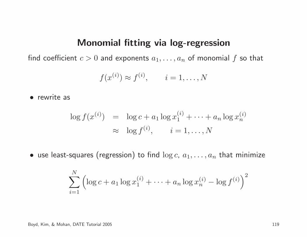
Monomial fitting via log-regression
find coefficient c > 0 and exponents a1, . . . , an of monomial f so that
f(x(i)) ≈ f (i), i = 1, . . . , N
• rewrite as
log f(x(i)) = log c + a1 log x(i)1 + · · · + an log x(i)
n
≈ log f (i), i = 1, . . . , N
• use least-squares (regression) to find log c, a1, . . . , an that minimize
N∑
i=1
(log c + a1 log x
(i)1 + · · · + an log x(i)
n − log f (i))2
Boyd, Kim, & Mohan, DATE Tutorial 2005 119

Posynomial fitting via Gauss-Newton
find coefficients and exponents of posynomial f so that
f(x(i)) ≈ f (i), i = 1, . . . , N
• minimize sum of squared fractional errors
N∑
i=1
(f (i) − f(x(i))
f (i)
)2
can be (locally) solved by Gauss-Newton method
• needs starting guess for coefficients, exponents
Boyd, Kim, & Mohan, DATE Tutorial 2005 120

Posynomial fitting example
• 1000 data points from f(x) = e(log x1)2+(log x2)
2over 0.1 ≤ xi ≤ 1
• cumulative error distribution for 3-, 5-, and 7-term posynomial fits
relative error in %
frac
tion
ofdat
apoi
nts
in%
bh3bh5
bh7
0 3.1 8 380
100
Boyd, Kim, & Mohan, DATE Tutorial 2005 121

A simple max-monomial fitting method
fit max-monomialf(x) = max
k=1,...,Kfk(x)
(f1, . . . , fk monomials) to data x(i), f (i), i = 1, . . . , N
simple algorithm:
repeat
for k = 1, . . . , K
1. find all data points x(j) for which fk(x(j)) = f(x(j))
(i.e., data points at which fk is the largest of the monomials)
2. update fk by carrying out monomial fit to these data
Boyd, Kim, & Mohan, DATE Tutorial 2005 122

Max-monomial fitting example
• same 1000 data points as previous example
• cumulative error distribution for 3-, 5-, and 7-term max-monomial fits
relative error in %
frac
tion
ofdat
apoi
nts
in%
0 0.1 0.2 0.3 0.4 0.50
100
bh3bh5
bh7
Boyd, Kim, & Mohan, DATE Tutorial 2005 123

Conclusions

Conclusions
(generalized) geometric programming
• comes up in a variety of circuit sizing contexts
• can be used to formulate a variety of problems
• admits fast, reliable solution of large-scale problems
• is good at concurrently balancing lots of coupled constraints andobjectives
• is useful even when problem has discrete constraints
Boyd, Kim, & Mohan, DATE Tutorial 2005 124

Approach
• most problems don’t come naturally in GP form; be prepared toreformulate and/or approximate
• GP modeling is not a “try my software” method; it requires thinking
• our approach:
– start with simple analytical models (RC, square-law, Pelgrom, . . . )to verify GP might apply
– then fit GP-compatible models to simulation or measured data– for highest accuracy, revert to local method for final polishing
Boyd, Kim, & Mohan, DATE Tutorial 2005 125

• looking for keys under street light(not where keys were lost, but lighting is good)
• forcing problems into GP-compatible form(problems aren’t GPs, but solving is good)
Boyd, Kim, & Mohan, DATE Tutorial 2005 126

References
• A tutorial on geometric programming
• Digital circuit sizing via geometric programming
• Analog circuit design via geometric programming
• Convex optimization, Cambridge Univ. Press 2004
(these include hundreds of references)
available at www.stanford.edu/~boyd/research.html
Boyd, Kim, & Mohan, DATE Tutorial 2005 127

Software
• MOSEK: www.mosek.com
• COPL-GP: (Yinyu Ye, in process of being re-worked):www.stanford.edu/~yyye/Col.html
• GPGLP: ftp://ftp.pitt.edu/dept/ie/GP/
• YALMIP: control.ee.ethz.ch/~joloef/yalmip.msql
• a simple matlab GP solver gp.m at Boyd’s EE364 site
Boyd, Kim, & Mohan, DATE Tutorial 2005 128


![Tractable Approximate Robust Geometric Programmingweb.stanford.edu/~boyd/papers/pdf/rgp-full.pdf · Tractable Approximate Robust Geometric Programming ... KC97], power control of](https://static.fdocuments.in/doc/165x107/5c9d5fd088c9939c348cafed/tractable-approximate-robust-geometric-boydpaperspdfrgp-fullpdf-tractable.jpg)