Generalized Time- and Transfer-Constant Circuit Analysis
17
TRANSACTIONS ON CIRCUITS AND SYSTEMS, VOL. XX, NO. XX, DECEMBER 2009 1 Generalized Time- and Transfer-Constant Circuit Analysis Ali Hajimiri, Abstract—The generalized method of time and transfer con- stants is introduced. It can be used to determine the transfer function to the desired level of accuracy in terms of time and transfer constants of first order systems using exclusively low frequency calculations. This method can be used to determine the poles and zeros of circuits with both inductors and capacitors. An inductive proof of this generalized method is given which subsumes special cases, such as methods of zero- and infinite- value time constants. Several important and useful corollaries of this method are discussed and several examples are analyzed. Index Terms—Circuit Analysis, method of time and trans- fer constants (TTC), determination of poles and zeros, zero- value time constants (ZVT), infinite-value time constants (IVT), Cochran-Grabel method, bandwidth enhancement techniques. I. I NTRODUCTION A NALOG circuit design depends on analysis as a beacon to provide qualitative and quantitative input on how we can improve circuit performance by modifying its topology and/or parameters. A great deal of effort goes into improving the accuracy of device models and circuit simulators to predict the expected experimental outcome accurately on a computer before testing going to the lab. However, these absolutely nec- essary tools are not sufficient for analog circuit design, which by its nature is open-ended and divergent. This necessitates analytical techniques that can provide insight into how and where the circuit can be modified for design purposes. The identification of the dominant source of a problem is at the core of design as it focuses creative energy on critical parts of the circuit and more importantly identify what kind of modifications will improve it. Generally, this is done by reducing the analysis into smaller more straightforward calculations that allow one to arrive at progressively more accurate approximations without performing the full analysis. Although mesh and nodal analysis provide a systematic framework to apply Kirchhoff’s current and voltage laws (KCL and KVL) to the circuit problem and convert them to a linear algebra problem (e.g., works of Bode [1] and Guillemin [2]) that can be solved numerically using a computer, they are not effective design tools. The analysis must be carried to the end before approximate results can be obtained and even then it is hard to obtain design insight from the resultant algebraic expressions particularly in terms of identifying the dominant A. Hajimiri is with the Department of Electrical Engineering, Cali- fornia Institute of Technology, Pasadena, CA, 91125 USA e-mail: ha- [email protected]. Manuscript received January 9, 2009; revised January 11, 2009. Copyright c 2008 IEEE. Personal use of this material is permitted. How- ever, permission to use this material for any other purposes must be obtained from the IEEE by sending an email to [email protected]. sources of problem and topological solutions to them. This need was recognized by some of the early works in this area, e.g., [3] and [4]. An early instance of an approach suitable for design is the method of open-circuit time constants (OCT) developed by Thornton, Searle, et al. in early 60’s [5]. The OCT was developed for lumped electronic circuits with capacitors as their sole energy storing (reactive) element to estimate their bandwidth limitation. It states that the coefficient of the term linear in complex frequency, s, in the denominator of the transfer function is exactly equal to the sum of time constants associated with each capacitor alone when all other capaci- tors are open circuited and sources are nulled. The original derivation of the OCT [5] and its subsequent generalizations to both capacitors and inductors, namely the method of zero value time-constants (ZVT), was based on evaluation of the determinant of the Y matrix in the nodal equations and how its co-factors change due to the capacitors [5]. The ZVT method is powerful since it provides a clear indication of the dominant source of bandwidth limitation and guidance into potential solutions. In Section IV, we present an alternative inductive derivation of ZVT’s and generalize using transfer constants to account for the effect of zeros on the bandwidth estimate The approach used in [5] was generalized in early 70’s by Cochran and Grabel [6] to determine as many of the denominator coefficients as needed by calculating the time- constants associated with each reactive element under differ- ent combinations of shorting and opening of other reactive elements in the circuit. Unlike nodal analysis, this process can be stopped at any point when the desired level of accuracy for the denominator has been obtained. The notation was cleaned further in the 80’s by Rosenstark to express denominator coefficient only in terms of time constants in a systematic way [10]. In the 90’s the method was generalized to include the effect of transcapacitors by Fox et al.[12] and mutual inductors by Andreani et al.[14]. In late 70’s Davis developed a method for determination of the numerator (and thus the zeros) of the transfer functions of lumped RC circuits using a combination of the time-constants and the low frequency transfer functions under different com- binations of shorting and opening of the capacitors [7]-[9]. We will discuss a generalization of this method with a more intuitive notation in Section V. The transfer function of a first order system can also be determined using the extra element theorem presented in late 80’s by Middlebrook [11]. In this case, two of the three low frequency calculations are identical to Davis’s approach [7]. The third calculation used to determine the numerator of
Transcript of Generalized Time- and Transfer-Constant Circuit Analysis
TRANSACTIONS ON CIRCUITS AND SYSTEMS, VOL. XX, NO. XX, DECEMBER 2009 1
Generalized Time- and Transfer-Constant CircuitAnalysis
Ali Hajimiri,
Abstract—The generalized method of time and transfer con-stants is introduced. It can be used to determine the transferfunction to the desired level of accuracy in terms of time andtransfer constants of first order systems using exclusively lowfrequency calculations. This method can be used to determine thepoles and zeros of circuits with both inductors and capacitors.An inductive proof of this generalized method is given whichsubsumes special cases, such as methods of zero- and infinite-value time constants. Several important and useful corollaries ofthis method are discussed and several examples are analyzed.
Index Terms—Circuit Analysis, method of time and trans-fer constants (TTC), determination of poles and zeros, zero-value time constants (ZVT), infinite-value time constants (IVT),Cochran-Grabel method, bandwidth enhancement techniques.
I. INTRODUCTION
ANALOG circuit design depends on analysis as a beaconto provide qualitative and quantitative input on how we
can improve circuit performance by modifying its topologyand/or parameters. A great deal of effort goes into improvingthe accuracy of device models and circuit simulators to predictthe expected experimental outcome accurately on a computerbefore testing going to the lab. However, these absolutely nec-essary tools are not sufficient for analog circuit design, whichby its nature is open-ended and divergent. This necessitatesanalytical techniques that can provide insight into how andwhere the circuit can be modified for design purposes.
The identification of the dominant source of a problemis at the core of design as it focuses creative energy oncritical parts of the circuit and more importantly identify whatkind of modifications will improve it. Generally, this is doneby reducing the analysis into smaller more straightforwardcalculations that allow one to arrive at progressively moreaccurate approximations without performing the full analysis.
Although mesh and nodal analysis provide a systematicframework to apply Kirchhoff’s current and voltage laws (KCLand KVL) to the circuit problem and convert them to a linearalgebra problem (e.g., works of Bode [1] and Guillemin [2])that can be solved numerically using a computer, they are noteffective design tools. The analysis must be carried to the endbefore approximate results can be obtained and even then itis hard to obtain design insight from the resultant algebraicexpressions particularly in terms of identifying the dominant
A. Hajimiri is with the Department of Electrical Engineering, Cali-fornia Institute of Technology, Pasadena, CA, 91125 USA e-mail: [email protected].
Manuscript received January 9, 2009; revised January 11, 2009.Copyright c©2008 IEEE. Personal use of this material is permitted. How-
ever, permission to use this material for any other purposes must be obtainedfrom the IEEE by sending an email to [email protected].
sources of problem and topological solutions to them. Thisneed was recognized by some of the early works in this area,e.g., [3] and [4].
An early instance of an approach suitable for design isthe method of open-circuit time constants (OCT) developedby Thornton, Searle, et al. in early 60’s [5]. The OCT wasdeveloped for lumped electronic circuits with capacitors astheir sole energy storing (reactive) element to estimate theirbandwidth limitation. It states that the coefficient of the termlinear in complex frequency, s, in the denominator of thetransfer function is exactly equal to the sum of time constantsassociated with each capacitor alone when all other capaci-tors are open circuited and sources are nulled. The originalderivation of the OCT [5] and its subsequent generalizationsto both capacitors and inductors, namely the method of zerovalue time-constants (ZVT), was based on evaluation of thedeterminant of the Y matrix in the nodal equations and how itsco-factors change due to the capacitors [5]. The ZVT methodis powerful since it provides a clear indication of the dominantsource of bandwidth limitation and guidance into potentialsolutions. In Section IV, we present an alternative inductivederivation of ZVT’s and generalize using transfer constants toaccount for the effect of zeros on the bandwidth estimate
The approach used in [5] was generalized in early 70’sby Cochran and Grabel [6] to determine as many of thedenominator coefficients as needed by calculating the time-constants associated with each reactive element under differ-ent combinations of shorting and opening of other reactiveelements in the circuit. Unlike nodal analysis, this process canbe stopped at any point when the desired level of accuracy forthe denominator has been obtained. The notation was cleanedfurther in the 80’s by Rosenstark to express denominatorcoefficient only in terms of time constants in a systematic way[10]. In the 90’s the method was generalized to include theeffect of transcapacitors by Fox et al.[12] and mutual inductorsby Andreani et al.[14].
In late 70’s Davis developed a method for determination ofthe numerator (and thus the zeros) of the transfer functions oflumped RC circuits using a combination of the time-constantsand the low frequency transfer functions under different com-binations of shorting and opening of the capacitors [7]-[9].We will discuss a generalization of this method with a moreintuitive notation in Section V.
The transfer function of a first order system can also bedetermined using the extra element theorem presented in late80’s by Middlebrook [11]. In this case, two of the threelow frequency calculations are identical to Davis’s approach[7]. The third calculation used to determine the numerator of
TRANSACTIONS ON CIRCUITS AND SYSTEMS, VOL. XX, NO. XX, DECEMBER 2009 2
the transfer function involves a null-double injection, whichinvolves simultaneous usage of two sources to null the outputsignal. The approach was generalized to N extra elements inlate 90’s in [13][15], where the denominator of the transferfunction is calculated the same way as the Cochron-Grabelmethod [6] and its numerator using multiple null doubleinjections. The approach presented in this paper does not usethe null double injection and provides a more intuitive linkbetween the zeros and the time and transfer constants.
In Section II, we discuss some of the general propertiesof a transfer function. We find the general transfer functionof a first order system in Section III, where the concept oftransfer constant is defined. Next we investigate an N th ordersystem and derive its first-order numerator and denominatorcoefficients. We provide an inductive intuitive proof and ageneralization of the method of zero-value time constantsand its generalization for the numerator using the concept oftransfer constant in Section IV. In Section V, we discuss howall the coefficients of the numerator and denominator can becalculated using the method of time and transfer constants(TTC) and thus provide a complete method to determine thetransfer function to the desired level of accuracy. Some of theimportant corollaries to circuit design will be discussed in VI.Finally, Section VII provides several examples of the method,which will be referred to through the text.
II. GENERAL PROPERTIES OF TRANSFER FUNCTIONS
For a single-input single-output linear time-invariant (LTI)network, the transfer function can be defined as the ratio ofthe voltages and/or currents of any two arbitrary ports of thecircuit, including the ratio of the voltage and current of thesame port. We designate the input and output variables as xand y. For example, when x is an input voltage due to a voltagesource and y is the voltage of another node in the circuit,the transfer function, H(s) ≡ vo(s)/vi(s), would correspondto a voltage gain. On the other hand, if the input, x, is thecurrent of a current source driving a given port of the circuit,while the output, y, is the voltage across the same port, thetransfer function, Z(s) ≡ v1(s)/i1(s) would correspond to theimpedance looking into that port1.
The transfer function of a linear system with lumped ele-ments can be written as2:
H(s) =a0 + a1s + a2s
2 + . . . + amsm
1 + b1s + b2s2 + . . . + bnsn(1)
where all ai and bj coefficients are real and s represents thecomplex frequency. Coefficient a0 is the low frequency (dc)
1One has to be careful about the choice of stimulus and output. If a nodeis excited with a current source and the voltage across that node is measured,then the quantity measured is the impedance, Z(s). On the other hand, ifthe same port is excited by a voltage source and its current is the outputvariable, the calculated transfer function is the admittance Y (s). Although inthe end we must have Z(s) = 1/Y (s), one should keep things consistent,as the poles of Z(s) are the zeros of Y (s) and vice versa. This is importantin nulling the independent source, which means a short-circuit for a voltagesource and an open-circuit for the current source.
2The leading one in the denominator is absent for transfer functions thatgo to infinity at dc (e.g., the input impedance of a capacitor to ground). Insuch cases, it is more straightforward to evaluate the inverse transfer function(e.g., admittance in the case of the capacitor).
transfer function. This equation can be factored as:3
H(s) = a0 ·(1− s
z1)(1− s
z2) . . . (1− s
zm)
(1− sp1
)(1− sp2
) . . . (1− spn
)(2)
where based on the fundamental theorem of algebra, the poleand zero frequencies (pi and zi) are either real or come ascomplex conjugate pairs.
The order of the denominator, n, determines the number ofnatural frequencies of the system and is equal to the numberof independent energy storage elements. This is equal to themaximum number of independent initial conditions (capacitorvoltages and inductor currents) that can be set, as we willsee later in Section V. Natural frequencies of the circuit areindependent of the choice of the input and output variablesand are intrinsic characteristics of the circuit4.
On the contrary, the zeros of the transfer function, i.e., theroots of the numerator of (1), do depend on the choice of theinput and output. While it is possible to answer what the polesof a circuit are without knowing what the input and outputvariables are, it is meaningless to ask the same question aboutthe zeros, as they assume different values for different choicesof the input and/or the output.
Knowing the coefficients of the transfer function of an LTIsystem (or equivalently its poles and zeros), we can predictits dynamics. In the following sections we see how we candetermine the transfer function of an N th order system tothe desired level of accuracy using low frequency calculationsof port resistances and low-frequency values of the transferfunctions (transfer constants) for different combinations ofshorting and opening of other elements. We will start withfirst order systems to elucidate the point, which is similar tothat in [7] with a modified, more generalizable notation:
III. FIRST ORDER SYSTEM
Let us consider an LTI circuit with a single energy-storingelement, an input x, and an output y, as shown in Figure 1aand b for a system with a capacitor or an inductor, respectively.Although these circuits include only one reactive element, C1
or L1, the network in the box can be quite complex with anynumber of frequency-independent elements, such as resistorsand dependent sources.
A circuit with one reactive element has one pole and onezero5. For a first order system, (1) reduces to:
H(s) =a0 + a1s
1 + b1s(3)
3The factorization of (1) is most suitable to describe a low-pass system. Inthe case of a band-pass amplifier with a well defined mid-band gain, amid,(where a0 can be very small or even zero) the poles and the zeros can bedivided into two groups: those occurring below mid-band and those that fallabove it. To have a flat pass-in this case, the number of poles and zeros belowmid-band must be equal. Thus, (2) can be reordered as (due to Middlebrook):
H(s) =(1− z1
s) . . . (1− zk
s)
(1− p1s
) . . . (1− pks
)· amid ·
(1− szk+1
) . . . (1− szm
)
(1− spk+1
) . . . (1− spn
)
This representation is helpful when we try to separate the effect of the polesand zeros affecting the low cut-off frequency, ωl, from those controlling thehigh cut-off frequency, ωh.
4The implicit assumption here is that these modes are observable in thecontrol theoretical sense.
5Sometime we say there is “no zero” when it is at infinity.

TRANSACTIONS ON CIRCUITS AND SYSTEMS, VOL. XX, NO. XX, DECEMBER 2009 3
Network with
no dynamics
C1
x y Network with
no dynamics
x y
L1
a) b)
Fig. 1. A first order system with a) a capacitor as the energy storing element,b) an inductor.
where a0 is the low-frequency transfer function. The pole willbe at p = −1/b1 corresponding to a pole time constant ofτ ≡ b1. The zero occurs at z = −a0/a1.
Now we use transfer constants defined as low frequencytransfer functions from the input to the output under differentcombinations of shorted and opened reactive elements (shownwith capital H with different superscripts) to determine of thetransfer function. Our first transfer constant is the value ofthe transfer function when the reactive element (or in generalall reactive elements) is (are) zero valued (C = 0, i.e., opencircuited capacitor and L = 0, i.e., short circuited inductor).This transfer constant is designated as H0. This is the same asthe low frequency transfer function since setting every reactiveelement to zero removes any frequency dependence from thecircuit, i.e.,
a0 = H0 (4)
For a first order system with a capacitor, C1, the only timeconstant, τ1, is simply R0
1C1, where R01 is the resistance
seen across the capacitor with all the independent sources(including the input) nulled. (Nulling a source means replacingan independent voltage source with a short circuit and anindependent current source with an open-circuit.) Here, thecircuit of Figure 1a simply reduces to the parallel combinationof capacitor, C1, and the low frequency resistance it sees, R0
1.Therefore, we have a pole time constant of
τ1 ≡ R01C1 = b1 (5)
where the superscript zero in R01 indicates that the independent
sources and the energy-storing element are at their zero valuesand the subscript is the index of the energy storing element.Equivalently, if the reactive element is an inductor, L1, thetime-constant is
τ1 ≡ L1
R01
. (6)
Let us continue with the case of capacitor for the time being.The impedance of the capacitor C1 is simply 1/C1s. We noticethat the capacitance, C1, and the complex frequency, s, alwaysappear together as a product, so the transfer function of (3)can be unambiguously written as:
H(s) =a0 + α1C1s
1 + β1C1s(7)
where α1 and β1 have the appropriate units. Combining (5)and (7), we obtain,
β1 = R01 (8)
We can use another transfer constant to determine thenumerator of (7). This time assume that the value of C1 goes toinfinity. For a capacitor this is equivalent to having it replacedwith a short circuit. For C1 → ∞, the second terms in thenumerator and the denominator of the transfer function of (7)dominate and hence it reduces to:
H1 ≡ H|C1→∞ =α1
β1(9)
where H1 is another transfer constant given from the inputx to the output y with the reactive element at its infinitevalue, e.g., capacitor C1 short circuited. This is simply anotherfrequency-independent gain calculation. Note that in generalthis transfer constant, H1, is different from the first transferconstant, H0, which is the low frequency transfer functionwith the energy storing element being zero valued (capacitoropen circuited or inductor shorted).
Considering (8)-(9) and comparing (3) to (7), we easilydetermine a1 to be:
a1 = α1C1 = R01C1H
1 = τ1H1 (10)
where τ1 is simply the pole time constant defined by (5) or(6).
The result of this derivation is that the transfer function of asystem with one energy-storing element can be expressed as:
H(s) =H0 + τ1H
1s
1 + τ1s(11)
where H0 is the zero-valued transfer constant from the input,x, to the output y when the reactive element is zero-valued(C1 opened or L1 shorted), H1 is the infinite-value transferconstant (C1 shorted or L1 opened), and τ1 is the time constantassociated with the reactive element and resistance it seeswith the independent sources nulled, R0
1. As can be seenfor a single energy-storing element, (11) provides the exacttransfer function of the system, in terms of three low-frequencycalculations.
IV. ZERO-VALUE TIME AND TRANSFER CONSTANTS
Having considered a system with one energy storage ele-ment, in this section we take the first step toward a completegeneralization of the approach to the case with N energystoring elements, which will be presented in Section V. Wewill start by determining the first term in the denominatorand numerator of (1), namely, b1 and a1 in a system with Nreactive (energy-storing) elements. First, using an alternativeinductive, more intuitive, derivation than that of [5], wedetermine b1 as the sum of the so-called zero-value timeconstants (ZVT) of the network6. Next, we also derive ageneral expression for a1 in terms of these ZVT’s and somelow frequency transfer functions.
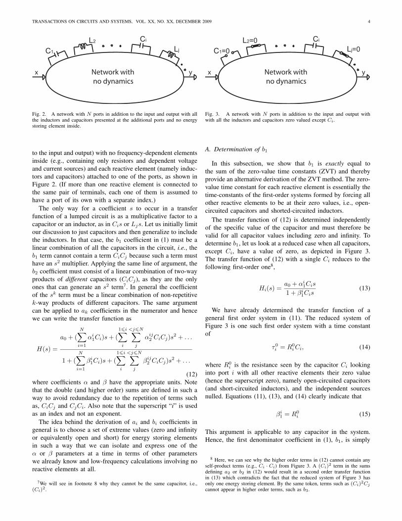
Any network with N energy-storing (reactive) elements canbe represented as a system with N external ports (in addition
6In [5], the first denominator term, b1, for capacitors only is derived usingan n-port nodal analysis of the above system and calculations of the co-factorsof the circuit determinant. It is generalized in [6] using a similar matrix-basedapproach.
TRANSACTIONS ON CIRCUITS AND SYSTEMS, VOL. XX, NO. XX, DECEMBER 2009 4
Network with
no dynamics
x y
Ci
LjC1
L2
Fig. 2. A network with N ports in addition to the input and output with allthe inductors and capacitors presented at the additional ports and no energystoring element inside.
to the input and output) with no frequency-dependent elementsinside (e.g., containing only resistors and dependent voltageand current sources) and each reactive element (namely induc-tors and capacitors) attached to one of the ports, as shown inFigure 2. (If more than one reactive element is connected tothe same pair of terminals, each one of them is assumed tohave a port of its own with a separate index.)
The only way for a coefficient s to occur in a transferfunction of a lumped circuit is as a multiplicative factor to acapacitor or an inductor, as in Cis or Ljs. Let us initially limitour discussion to just capacitors and then generalize to includethe inductors. In that case, the b1 coefficient in (1) must be alinear combination of all the capacitors in the circuit, i.e., theb1 term cannot contain a term CiCj because such a term musthave an s2 multiplier. Applying the same line of argument, theb2 coefficient must consist of a linear combination of two-wayproducts of different capacitors (CiCj), as they are the onlyones that can generate an s2 term7. In general the coefficientof the sk term must be a linear combination of non-repetitivek-way products of different capacitors. The same argumentcan be applied to ak coefficients in the numerator and hencewe can write the transfer function as
H(s) =
a0 + (N∑
i=1
αi1Ci)s + (
16i∑
i
<j6N∑
j
αij2 CiCj)s2 + . . .
1 + (N∑
i=1
βi1Ci)s + (
16i∑
i
<j6N∑
j
βij2 CiCj)s2 + . . .
(12)where coefficients α and β have the appropriate units. Notethat the double (and higher order) sums are defined in such away to avoid redundancy due to the repetition of terms suchas, CiCj and CjCi. Also note that the superscript “i” is usedas an index and not an exponent.
The idea behind the derivation of ai and bi coefficients ingeneral is to choose a set of extreme values (zero and infinityor equivalently open and short) for energy storing elementsin such a way that we can isolate and express one of theα or β parameters at a time in terms of other parameterswe already know and low-frequency calculations involving noreactive elements at all.
7We will see in footnote 8 why they cannot be the same capacitor, i.e.,(Ci)
2.
Network with
no dynamics
x y
Ci
Lj=0C1=0
L2=0
Fig. 3. A network with N ports in addition to the input and output withwith all the inductors and capacitors zero valued except Ci.
A. Determination of b1
In this subsection, we show that b1 is exactly equal tothe sum of the zero-value time constants (ZVT) and therebyprovide an alternative derivation of the ZVT method. The zero-value time constant for each reactive element is essentially thetime-constants of the first-order systems formed by forcing allother reactive elements to be at their zero values, i.e., open-circuited capacitors and shorted-circuited inductors.
The transfer function of (12) is determined independentlyof the specific value of the capacitor and must therefore bevalid for all capacitor values including zero and infinity. Todetermine b1, let us look at a reduced case when all capacitors,except Ci, have a value of zero, as depicted in Figure 3.The transfer function of (12) with a single Ci reduces to thefollowing first-order one8,
Hi(s) =a0 + αi
1Cis
1 + βi1Cis
(13)
We have already determined the transfer function of ageneral first order system in (11). The reduced system ofFigure 3 is one such first order system with a time constantof
τ0i = R0
i Ci, (14)
where R0i is the resistance seen by the capacitor Ci looking
into port i with all other reactive elements their zero value(hence the superscript zero), namely open-circuited capacitors(and short-circuited inductors), and the independent sourcesnulled. Equations (11), (13), and (14) clearly indicate that
βi1 = R0
i (15)
This argument is applicable to any capacitor in the system.Hence, the first denominator coefficient in (1), b1, is simply
8 Here, we can see why the higher order terms in (12) cannot contain anyself-product terms (e.g., Ci · Ci) from Figure 3. A (Ci)
2 term in the sumsdefining a2 or b2 in (12) would result in a second order transfer functionin (13) which contradicts the fact that the reduced system of Figure 3 hasonly one energy storing element. By the same token, terms such as (Ci)
2Cj
cannot appear in higher order terms, such as b3.
TRANSACTIONS ON CIRCUITS AND SYSTEMS, VOL. XX, NO. XX, DECEMBER 2009 5
Network with
no dynamics
x y
Ci →∞Lj=0C1=0
L2=0
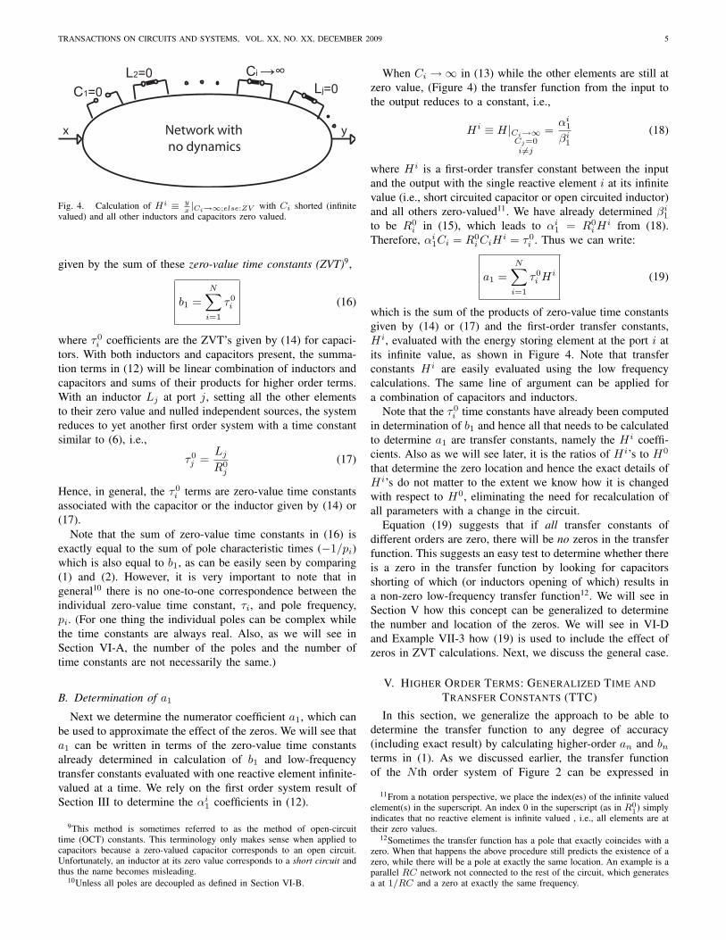
Fig. 4. Calculation of Hi ≡ yx|Ci→∞;else:ZV with Ci shorted (infinite
valued) and all other inductors and capacitors zero valued.
given by the sum of these zero-value time constants (ZVT)9,
b1 =N∑
i=1
τ0i (16)
where τ0i coefficients are the ZVT’s given by (14) for capaci-
tors. With both inductors and capacitors present, the summa-tion terms in (12) will be linear combination of inductors andcapacitors and sums of their products for higher order terms.With an inductor Lj at port j, setting all the other elementsto their zero value and nulled independent sources, the systemreduces to yet another first order system with a time constantsimilar to (6), i.e.,
τ0j =
Lj
R0j
(17)
Hence, in general, the τ0i terms are zero-value time constants
associated with the capacitor or the inductor given by (14) or(17).
Note that the sum of zero-value time constants in (16) isexactly equal to the sum of pole characteristic times (−1/pi)which is also equal to b1, as can be easily seen by comparing(1) and (2). However, it is very important to note that ingeneral10 there is no one-to-one correspondence between theindividual zero-value time constant, τi, and pole frequency,pi. (For one thing the individual poles can be complex whilethe time constants are always real. Also, as we will see inSection VI-A, the number of the poles and the number oftime constants are not necessarily the same.)
B. Determination of a1
Next we determine the numerator coefficient a1, which canbe used to approximate the effect of the zeros. We will see thata1 can be written in terms of the zero-value time constantsalready determined in calculation of b1 and low-frequencytransfer constants evaluated with one reactive element infinite-valued at a time. We rely on the first order system result ofSection III to determine the αi
1 coefficients in (12).
9This method is sometimes referred to as the method of open-circuittime (OCT) constants. This terminology only makes sense when applied tocapacitors because a zero-valued capacitor corresponds to an open circuit.Unfortunately, an inductor at its zero value corresponds to a short circuit andthus the name becomes misleading.
10Unless all poles are decoupled as defined in Section VI-B.
When Ci →∞ in (13) while the other elements are still atzero value, (Figure 4) the transfer function from the input tothe output reduces to a constant, i.e.,
Hi ≡ H|Ci→∞Cj=0i 6=j
=αi
1
βi1
(18)
where Hi is a first-order transfer constant between the inputand the output with the single reactive element i at its infinitevalue (i.e., short circuited capacitor or open circuited inductor)and all others zero-valued11. We have already determined βi
1
to be R0i in (15), which leads to αi
1 = R0i H
i from (18).Therefore, αi
1Ci = R0i CiH
i = τ0i . Thus we can write:
a1 =N∑
i=1
τ0i Hi (19)
which is the sum of the products of zero-value time constantsgiven by (14) or (17) and the first-order transfer constants,Hi, evaluated with the energy storing element at the port i atits infinite value, as shown in Figure 4. Note that transferconstants Hi are easily evaluated using the low frequencycalculations. The same line of argument can be applied fora combination of capacitors and inductors.
Note that the τ0i time constants have already been computed
in determination of b1 and hence all that needs to be calculatedto determine a1 are transfer constants, namely the Hi coeffi-cients. Also as we will see later, it is the ratios of Hi’s to H0
that determine the zero location and hence the exact details ofHi’s do not matter to the extent we know how it is changedwith respect to H0, eliminating the need for recalculation ofall parameters with a change in the circuit.
Equation (19) suggests that if all transfer constants ofdifferent orders are zero, there will be no zeros in the transferfunction. This suggests an easy test to determine whether thereis a zero in the transfer function by looking for capacitorsshorting of which (or inductors opening of which) results ina non-zero low-frequency transfer function12. We will see inSection V how this concept can be generalized to determinethe number and location of the zeros. We will see in VI-Dand Example VII-3 how (19) is used to include the effect ofzeros in ZVT calculations. Next, we discuss the general case.
V. HIGHER ORDER TERMS: GENERALIZED TIME ANDTRANSFER CONSTANTS (TTC)
In this section, we generalize the approach to be able todetermine the transfer function to any degree of accuracy(including exact result) by calculating higher-order an and bn
terms in (1). As we discussed earlier, the transfer functionof the N th order system of Figure 2 can be expressed in
11From a notation perspective, we place the index(es) of the infinite valuedelement(s) in the superscript. An index 0 in the superscript (as in R0
1) simplyindicates that no reactive element is infinite valued , i.e., all elements are attheir zero values.
12Sometimes the transfer function has a pole that exactly coincides with azero. When that happens the above procedure still predicts the existence of azero, while there will be a pole at exactly the same location. An example is aparallel RC network not connected to the rest of the circuit, which generatesa at 1/RC and a zero at exactly the same frequency.
TRANSACTIONS ON CIRCUITS AND SYSTEMS, VOL. XX, NO. XX, DECEMBER 2009 6
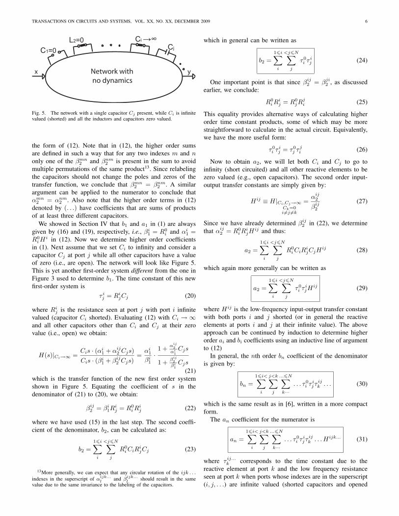
Network with
no dynamics
x y
Ci →∞
C1=0
L2=0Cj
Fig. 5. The network with a single capacitor Cj present, while Ci is infinitevalued (shorted) and all the inductors and capacitors zero valued.
the form of (12). Note that in (12), the higher order sumsare defined in such a way that for any two indexes m and nonly one of the βmn
2 and βnm2 is present in the sum to avoid
multiple permutations of the same product13. Since relabelingthe capacitors should not change the poles and zeros of thetransfer function, we conclude that βmn
2 = βnm2 . A similar
argument can be applied to the numerator to conclude thatαmn
2 = αnm2 . Also note that the higher order terms in (12)
denoted by (. . .) have coefficients that are sums of productsof at least three different capacitors.
We showed in Section IV that b1 and a1 in (1) are alwaysgiven by (16) and (19), respectively, i.e., βi
1 = R0i and αi
1 =R0
i Hi in (12). Now we determine higher order coefficients
in (1). Next assume that we set Ci to infinity and consider acapacitor Cj at port j while all other capacitors have a valueof zero (i.e., are open). The network will look like Figure 5.This is yet another first-order system different from the one inFigure 3 used to determine b1. The time constant of this newfirst-order system is
τ ij = Ri
jCj (20)
where Rij is the resistance seen at port j with port i infinite
valued (capacitor Ci shorted). Evaluating (12) with Ci → ∞and all other capacitors other than Ci and Cj at their zerovalue (i.e., open) we obtain:
H(s)|Ci→∞ =Cis · (αi
1 + αij2 Cjs)
Cis · (βi1 + βij
2 Cjs)=
αi1
βi1
·1 + αij
2αi
1Cjs
1 + βij2
βi1Cjs
(21)which is the transfer function of the new first order systemshown in Figure 5. Equating the coefficient of s in thedenominator of (21) to (20), we obtain:
βij2 = βi
1Rij = R0
i Rij (22)
where we have used (15) in the last step. The second coeffi-cient of the denominator, b2, can be calculated as:
b2 =16i∑
i
<j6N∑
j
R0i CiR
ijCj (23)
13More generally, we can expect that any circular rotation of the ijk . . .indexes in the superscript of αijk...
land βijk...
lshould result in the same
value due to the same invariance to the labeling of the capacitors.
which in general can be written as
b2 =16i∑
i
<j6N∑
j
τ0i τ i
j (24)
One important point is that since βij2 = βji
2 , as discussedearlier, we conclude:
R0i R
ij = R0
jRji (25)
This equality provides alternative ways of calculating higherorder time constant products, some of which may be morestraightforward to calculate in the actual circuit. Equivalently,we have the more useful form:
τ0i τ i
j = τ0j τ j
i (26)
Now to obtain a2, we will let both Ci and Cj to go toinfinity (short circuited) and all other reactive elements to bezero valued (e.g., open capacitors). The second order input-output transfer constants are simply given by:
Hij ≡ H|Ci,Cj→∞Ck=0i 6=j 6=k
=αij
2
βij2
(27)
Since we have already determined βij2 in (22), we determine
that αij2 = R0
i RijH
ij and thus:
a2 =16i∑
i
<j6N∑
j
R0i CiR
ijCjH
ij (28)
which again more generally can be written as
a2 =16i∑
i
<j6N∑
j
τ0i τ i
jHij (29)
where Hij is the low-frequency input-output transfer constantwith both ports i and j shorted (or in general the reactiveelements at ports i and j at their infinite value). The aboveapproach can be continued by induction to determine higherorder ai and bi coefficients using an inductive line of argumentto (12)
In general, the nth order bn coefficient of the denominatoris given by:
bn =16i<∑
i
j<k∑
j
...6N∑
k···. . . τ0
i τ ijτ
ijk . . . (30)
which is the same result as in [6], written in a more compactform.
The an coefficient for the numerator is
an =16i<∑
i
j<k∑
j
...6N∑
k···. . . τ0
i τ ijτ
ijk . . . Hijk... (31)
where τ ij...k corresponds to the time constant due to the
reactive element at port k and the low frequency resistanceseen at port k when ports whose indexes are in the superscript(i, j, . . .) are infinite valued (shorted capacitors and opened
TRANSACTIONS ON CIRCUITS AND SYSTEMS, VOL. XX, NO. XX, DECEMBER 2009 7
inductors). In the presence of inductors a similar line ofargument can be applied, noting that the time constant τ ij...
k
associated with inductor Lk is simply the inductance dividedby Rij...
k which is the resistance seen at port k with the reactiveelements at ports i, j, . . . at their infinite values14. So the timeconstants in (30) and (31) will have one of the followingforms depending on whether there is an inductor or a capacitorconnected to port k. For capacitor, Ci:
τ jk...i = CiR
jk...i (33)
and for inductor, Ll:
τmn...l =
Ll
Rmn...l
(34)
Finally, Hijk... is the nth-order transfer constant evaluatedwith the energy storing elements at ports i, j, k, . . . at theirinfinite values (shorted capacitors and opened inductors) andall others zero valued (opened capacitors and shorted induc-tors). It is noteworthy that (30) indicates that the poles of thetransfer function are independent of the definition of inputand output and are only characteristics of the network itself,while the zeros are not a global property of the circuit anddepend on the definition of the input and output ports andvariables, as evident from the presence of the Hij... terms.This is consistent with the fact that poles are the roots of thedeterminant of the Y matrix [1] defined independent of theinput and output ports.
Several observations are in order about this approach. Firstof all this approach is exact and makes it possible to determinethe transfer function completely and exactly. More importantly,unlike writing nodal or mesh equations, one does not need tocarry the analysis to its end to be able to obtain useful infor-mation about the circuit. Additional information about higherorder poles and zeros can be obtained by carrying the analysisthrough enough steps to obtain the results to the desired levelof accuracy. Also, the analysis is equally applicable to realand complex poles and zeros. Once mastered, this analysismethod provides a fast and insightful means of evaluatingtransfer functions, as well as input and output impedances forgeneral circuits. The generalized time and transfer constants(TTC) approach has several important and useful corollariesthat will be discussed in the next Section.
VI. COROLLARIES AND APPLICATIONS
A. Number of Poles and Zeros
It is a well known result that the number of poles (i.e.,the number of natural frequencies) of a circuit is equal to themaximum number of independent initial conditions we canset for energy-storing elements. This result can also be easilydeduced from (30), where the highest order non-zero bn isdetermined by the highest order non-zero time constant, τ jk...
i
in the system.
14 Equations (25) can be generalized noting the invariance of the βijk...l
to a rotation of the indexes to produce
R0i Ri
jRijk
. . . Rijk...m = R0
jRjk
. . . Rjkl...m Rjkl...
i (32)
It is easy to see that each purely capacitive loop with noother elements in the loop reduces the order of the system byone. This is because the highest order time constant associatedwith the last capacitor, when all the other ones are infinitevalued (shorted) is zero, since the resistance seen by thatcapacitor in that case is zero15 (see Example VII-2 in SectionVII). The same effect holds for an inductive cut-set, whereonly inductors are attached to a node. Again the time constantassociated with the last inductor, when all others are infinite-valued (opened) is zero since the resistance seen is infinity.
The number of zeros can also be determined easily in theapproach presented here. The number of zeros is determinedby the order of the numerator polynomial, which is in turneddetermined by the highest order non-zero transfer constant,Hijk..., in (31). In other words, the number of zeros inthe circuit is equal to the maximum number of energy-storing elements that can be simultaneously infinite-valuedwhile producing a non-zero transfer constant Hijk... fromthe input to the output. This way we can easily determinehow many zeros there are in the transfer function of thesystem by inspection without having to write any equations(see Examples VII-2, VII-3, and VII-8). This is one of theadvantages of this approach over that presented in [15].
B. Decoupled PolesThe second important corollary of the TTC relates to
decoupled poles of the circuits. As we mentioned in subsectionIV-A, there is no one-to-one correspondence between the zero-valued time constants, τ0
i and the poles’ characteristic times(−1/pi). However, an important exception is when a time-constant is decoupled from all other ones. This happens when atime constant does not change for any combination of shortingand opening of other energy-storing elements, i.e., in ournotation,
τ0N = τ i
N = τ ijN = · · · = τ ij...m
N (35)
In this case, the term (1 + τ0Ns) can be factored out of the
denominator16 and the pole associated with it is simply a real
15In general, in a circuit with N +1 nodes (including ground) we can haveup to N(N + 1)/2 distinct capacitors connected among the nodes. Despitethis potentially large number of distinct capacitors, we can only define Nindependent initial conditions. This can be seen if we assume that the voltagesbetween individual capacitors from each node to ground is set. This sets all thenode voltages and thus no more initial condition can be defined independently,meaning we can have a maximum of N poles in such a circuit.
16This can be proved rather easily by reordering the terms of the denomi-nator as:
D(s) = 1 + b1s + b2s2 + · · ·
= 1 + s
N∑i=1
τ0i + s2
16i∑i
<j6N∑j
τ0i τ i
j + · · ·
= 1 + s(τ0N +
N−1∑i=1
τ0i ) + s2(
N−1∑i=1
τ0i τ i
N +
16i<∑i
j6N−1∑j
τ0i τ i
j ) + · · ·
= (1 + sτ0N ) + (1 + sτ0
N )s
N−1∑i=1
τ0i + (1 + sτ0
N )s2
16i<∑i
j6N−1∑j
τ0i τ i
j + · · ·
= (1 + sτ0N )
[1 + s
N−1∑i=1
τ0i + s2
16i∑i
<j6N−1∑j
τ0i τ i
j · · ·]
(36)

TRANSACTIONS ON CIRCUITS AND SYSTEMS, VOL. XX, NO. XX, DECEMBER 2009 8
one at pN = −1/τ0N .
This concept can be generalized to a group or groupsof time constants that can be decoupled from the rest ofthe time constants but internally coupled. An example is amulti-stage amplifier, with no interstage capacitors, wherethe time constants within each stage may be coupled andcannot be factored into products of first order terms, however,it is possible to factor the numerator and denominator intoproduct of lower order polynomials each associated with oneset of externally uncoupled yet internally coupled set of timeconstants internal to each stage. This can be viewed as apartitioning of time constants into these mutually uncoupledsubsets. (See Example VII-4).
C. Bandwidth Estimation using ZVT’s
The b1 coefficient calculated in (16) can be used to form afirst-order estimate of ωh, the −3dB bandwidth of a circuitwith a low-pass response17. More importantly, it is a powerfuldesign tool allowing the designer to identify the primarysource of bandwidth limitation and can serve as a guide inmaking qualitative (e.g., topological) and quantitative (e.g.,element values) changes to the circuit.
There are several simplifying assumptions involved in ap-plication of the basic ZVT method to bandwidth estimation.The original ZVT approach [5] assumes that there are no(dominant) zeros in the transfer function. Next in subsectionVI-D, we will augment the approach to account for dominantzeros in the transfer function and how to determine if they arepresent.
For now let us assume there are no dominant zeros in thetransfer function. In this case, the transfer function can beapproximated as
H(s) ≈ a0
1 + b1s + b2s2 + . . . + bnsn(37)
which is the transfer function of low-pass system with a low-frequency value of a0.
At dc (s = 0), the only term in the denominator that mattersis the leading 1. As the frequency goes up and approaches ωh,the first term that becomes non-negligible would be b1s, so inthe vicinity of the ωh, (37) can be further approximated as afirst order system
H(s) ≈ a0
1 + b1s(38)
This implies that ωh, bandwidth of the complete system, canbe approximated as[5]:
ωh ≈ 1b1
=1
N∑
i=1
τ0i
(39)
where the term in the bracket is of order of sn−1.17As we saw in section II, we can split a bandpass response with a well-
defined mid-band gain into a low-pass and a high-pass one. We can arriveat the low pass response by setting certain biasing elements such as bypasscapacitors, coupling capacitors, and RF chokes to their infinite values (shortedcapacitor and open inductor). Then using the method of zero-value timeconstants we can approximate ωh. A dual process called the method ofinfinite-value time (IVT) constants discussed in section VI-G can be use toestimate ωl in the high-pass system.
where τ0i are the zero value time constants defined by (14) and
(17) for capacitors and inductors, respectively18. This approx-imation is conservative and underestimates the bandwidth[16].
As mentioned earlier, the coefficient b1 is the sum ofthe pole characteristic times (−1/pi) with no one-to-onecorresponds among pi’s and τi’s, in general. Therefore, theimaginary parts of complex conjugate pole pairs cancel eachother in the b1 sum. As a result, ZVT method by itself doesnot provide any information about the imaginary part of thepoles and is completely oblivious to it. This can result in grossunderestimation of the bandwidth using (39), when the circuithas dominant complex poles which could lead to peaking inthe frequency response. We will see how we can determinewhether or not complex poles are present and how to estimatetheir quality factor (Q) in Section VI-F and Example VII-5.
D. Modified ZVT Bandwidth Estimation for a System withZeros
The ZVT approximation of (39) can be improved in the lightof (19). In the presence of zeros using a similar argument usedto arrive at (38), we conclude that close to ωh, the transferfunction can be estimated as:
H(s) ≈ a0 ·1 + a1
a0s
1 + b1s(40)
which is a first order system with a pole at −1/b1 and a zero at−a0/a1. The zero has the opposite effect on the magnitude ofthe transfer function compared to the pole since it increases themagnitude of the transfer function with frequency. Accordingto (19), we have,
a1
a0=
N∑
i=1
τ0i
Hi
H0(41)
First, let us assume that all Hi/H0 terms are positive. Inthis case, the numerator’s first order coefficient, a1/a0, willbe positive and the dominant zero is left-half plane (LHP).In this case, using the first Taylor series expansion terms ofthe numerator and the denominator, the ωh estimate can bemodified to
ωh ≈ 1b1 − a1
a0
=1
N∑
i=1
τ0i (1− Hi
H0)
(42)
If some of the Hi/H0 terms are negative, it means that thetransfer function has right-half plane (RHP) zeros. However,the RHP zeros have exactly the same effect on the amplitude asLHP ones unlike their phase response. Since ωh only dependson the amplitude response and not the phase, a LHP zero at agiven frequency should produce the exact same ωh as a RHPzero at the same frequency. Therefore, in general, a better
18Intuitively, ωh is the frequency at which the total output amplitude dropsby a factor of
√2 with respect to a0. Under normal circumstances, at this point
the contribution of each one of the energy-storing elements is relatively smalland hence (39) can be thought of as the sum of their individual contributionsto the gain reduction, assuming the other ones are not present.
TRANSACTIONS ON CIRCUITS AND SYSTEMS, VOL. XX, NO. XX, DECEMBER 2009 9
approximation for ωh (assuming it exists) is
ωh ≈ 1N∑
i=1
τ0i
(43)
where
τ0i = τ0
i · (1− |Hi
H0|) (44)
are modified ZVT’s that are only different from the originalZVT’s for reactive element which result in non-zero transferconstants when infinite valued (e.g., capacitors shorting ofwhich does not make the gain zero). Also note that (43) and(44) subsume (42) for LHP zeros and reduces to (39) whenthere are no zeros, i.e., all Hi terms are zero (correspondingto a1 = 0). Usually only a few of the original ZVT’s needbe modified. Note that the correction to the time constantscan be done at the same time they are calculated simply byevaluating the change in the low frequency transfer functionwhen the element is infinite valued.
Example VII-3 shows how the modified ZVT’s produce auseful result in the presence of zeros, while regular ZVT’sresult is substantially inaccurate.
E. The Creation and Effect of Zeros
Unlike poles that are natural frequencies of the circuit andhence are not affected by the choice of the input and outputvariables, zeros change with the choice of the input and outputvariables, as evident by the presence of Hijk... terms in thean’s. As mentioned earlier, as long as infinite valuing of somereactive elements results in non-zero low-frequency transferfunction, there are zeros in the system.
1) Zeros in a First-Order System: For a first-order systemwith a single energy-storing element, we can easily obtain thefollowing relation between the pole and the zero from (11):
z =H0
H1· p (45)
This expression is sufficient to evaluate the relative position ofthe zero with respect to the pole. It is clear from (45) that if theinfinite- and zero-value transfer constants have opposite signs,the pole and the zero will be on two opposite half-planes. Forinstance, these correspond to low frequency gain of the systemwith a capacitor short- and open-circuited. In stable systemswhere the pole is in the LHP, the zero will be on the RHP foropposite polarities of H0 and H1, as in Example VII-2. Onthe other hand if H0 and H1 have the same polarity, the poleand the zero will be both on the LHP (see Example VII-3).
The magnitude of H0/H1 determines which one occurs ata lower frequency. As evident from (45), the zero happensfirst (at a lower frequency than the pole, i.e., |z| < |p|) when|H0/H1| < 1. Alternatively, the pole occurs before the zero(|p| < |z|), for |H0/H1| > 1. This assessment can almostalways be done by inspection because we only need to knowthe relative size and magnitude of H0 and H1, as summarizedin Table I.
t
s1(t) s2(t) s(t)
t t
H0
H1
H1
H0
+ =
Fig. 6. The step response of a first order system decomposed as the sumof the step response of a first-order low-pass system, s1(t) and high-passsystems, s2(t).
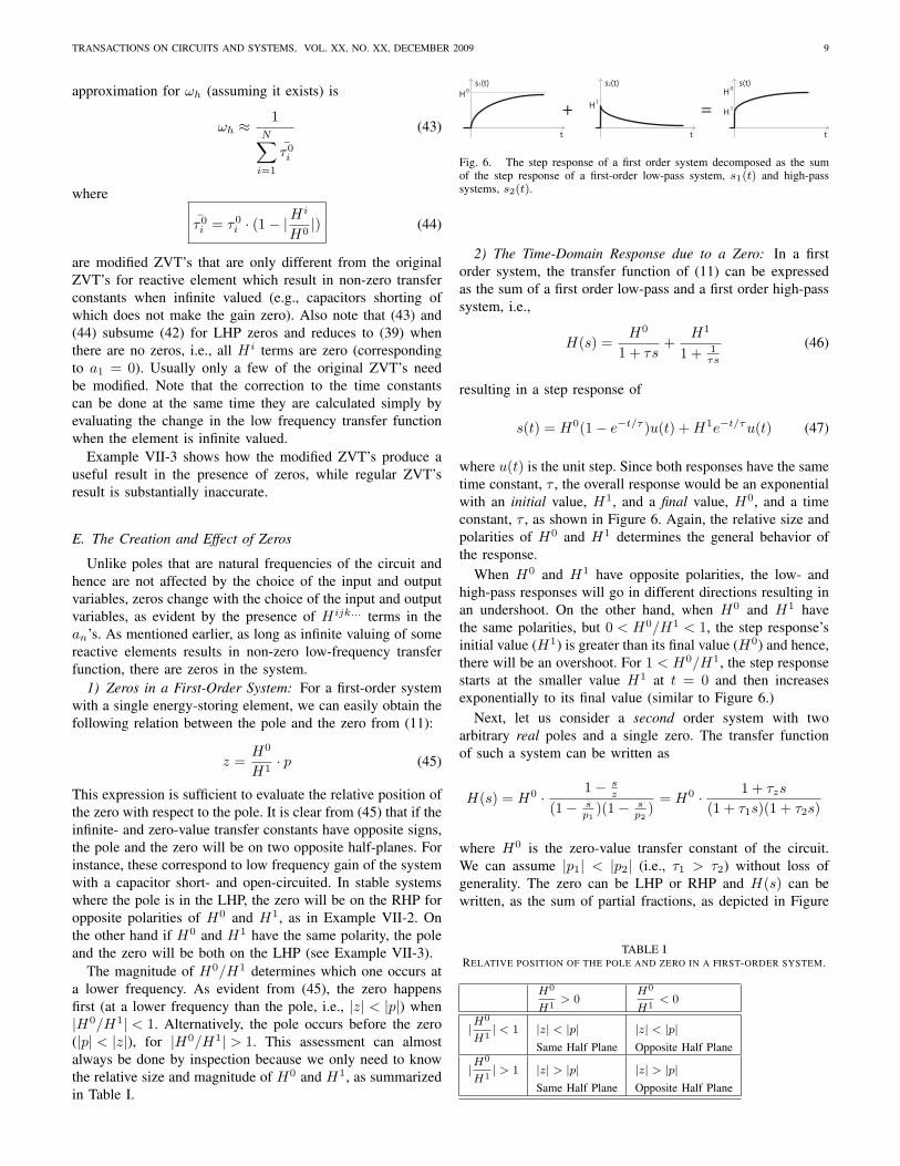
2) The Time-Domain Response due to a Zero: In a firstorder system, the transfer function of (11) can be expressedas the sum of a first order low-pass and a first order high-passsystem, i.e.,
H(s) =H0
1 + τs+
H1
1 + 1τs
(46)
resulting in a step response of
s(t) = H0(1− e−t/τ )u(t) + H1e−t/τu(t) (47)
where u(t) is the unit step. Since both responses have the sametime constant, τ , the overall response would be an exponentialwith an initial value, H1, and a final value, H0, and a timeconstant, τ , as shown in Figure 6. Again, the relative size andpolarities of H0 and H1 determines the general behavior ofthe response.
When H0 and H1 have opposite polarities, the low- andhigh-pass responses will go in different directions resulting inan undershoot. On the other hand, when H0 and H1 havethe same polarities, but 0 < H0/H1 < 1, the step response’sinitial value (H1) is greater than its final value (H0) and hence,there will be an overshoot. For 1 < H0/H1, the step responsestarts at the smaller value H1 at t = 0 and then increasesexponentially to its final value (similar to Figure 6.)
Next, let us consider a second order system with twoarbitrary real poles and a single zero. The transfer functionof such a system can be written as
H(s) = H0 · 1− sz
(1− sp1
)(1− sp2
)= H0 · 1 + τzs
(1 + τ1s)(1 + τ2s)
where H0 is the zero-value transfer constant of the circuit.We can assume |p1| < |p2| (i.e., τ1 > τ2) without loss ofgenerality. The zero can be LHP or RHP and H(s) can bewritten, as the sum of partial fractions, as depicted in Figure
TABLE IRELATIVE POSITION OF THE POLE AND ZERO IN A FIRST-ORDER SYSTEM.
H0
H1> 0
H0
H1< 0
|H0
H1| < 1 |z| < |p| |z| < |p|
Same Half Plane Opposite Half Plane
|H0
H1| > 1 |z| > |p| |z| > |p|
Same Half Plane Opposite Half Plane
TRANSACTIONS ON CIRCUITS AND SYSTEMS, VOL. XX, NO. XX, DECEMBER 2009 10
R1
R2
C1
A1
C2
A2
vin vout+
+
slow path
fast path
Fig. 7. A system consisting of two signal paths each with a first orderresponse followed by unilateral ideal voltage amplifiers.
7 [17]19
H(s) =A1
1− sp1
+A2
1− sp2
=A1
1 + τ1s+
A2
1 + τ2s(49)
where τ1 = −1/p1 and τ2 = −1/p2 are the pole characteristictimes (τ1 > τ2) and we have,
τz = −1z
=A2τ1 + A1τ2
A1 + A2(50)
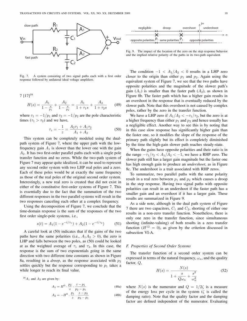
This system can be completely modeled using the dual-path system of Figure 7, where the upper path with the low-frequency gain A1 is slower than the lower one with the gainA2. It has two first-order parallel paths each with a single poletransfer function and no zeros. While the two-path system ofFigure 7 may appear quite idealized, it can be used to representany second order system with two LHP real poles and a zero.Each of these poles would be at exactly the same frequencyas those of the real poles of the original second order system.Interestingly, a new real zero is created that did not exist ineither of the constitutive first-order systems of Figure 7. Thisis essentially due to the fact that the summation of the twodifferent responses in the two parallel systems will result in thetwo responses canceling each other at a complex frequency.
Using the decomposition of Figure 7, we conclude that thetime-domain response is the sum of the responses of the twofirst order single-pole systems, i.e.,
s(t) = A1(1− e−t/τ1) + A2(1− e−t/τ2) (51)
A careful look at (50) indicates that if the gains of the twopaths have the same polarities (i.e., A1A2 > 0), the zero isLHP and falls between the two poles, as (50) could be lookedat as the weighted average of τ1 and τ2. In this case, theresponse is the sum of two exponentials going in the samedirection with two different time constants as shown in Figure8a, resulting in a droop, as the response associated with p2
settles quickly but the response corresponding to p1 takes awhile longer to reach its final value.
19A1 and A2 are given by:
A1 = H0 · p2
z· z − p1
p2 − p1(48a)
A2 = −H0 · p1
z· z − p2
p2 − p1(48b)
P1 P2
droop overshootnegligible undershoot
opposite polaritiessame polaritiesopposite polarities
jω
σ
Fig. 9. The impact of the location of the zero on the step response behaviorand the implied relative polarity of the paths in its two-path equivalent.
The condition −1 < A1/A2 < 0 results in a LHP zerocloser to the origin than either p1 and p2. Again using theequivalent system of Figure 7, we see that the two paths haveopposite polarities and the magnitude of the slower path’sgain (A1) is smaller than the faster path (A2), as shown inFigure 8b. The faster path which has a higher gain results inan overshoot in the response that is eventually reduced by theslower path. Note that this overshoot is not caused by complexpoles, rather by the zero in the transfer function.
We have a LHP zero if A1/A2 < −τ1/τ2, but the zero is ata higher frequency than either p1 and p2 and hence usually hasa negligible effect. Another way to see this is by noting thatin this case slow response has significantly higher gain thanthe faster one, so it modifies the slope of the response of theprimary path slightly but its effect is completely diminishedby the time the high-gain slower path reaches steady-state.
When the gains have opposite polarities and their ratio is inthe range −τ1/τ2 < A1/A2 < −1, we have a RHP zero. Theslower path still has a larger gain magnitude but the faster onehas high enough gain to produce an undershoot, as in Figure8c. The undershoot is a trait associated with RHP zeros.
To summarize, two parallel paths with the same polarityresult in a real zero between p1 and p2 which causes a droopin the step response. Having two signal paths with oppositepolarities can result in an undershoot if the faster path has asmaller gain and an overshoot if it has a larger gain. Theseresults are summarized in Figure 9.
As a side note, although in the dual path system of Figure7 there are two capacitors, C1 and C2, shorting of either oneresults in a non-zero transfer function. Nonetheless, there isonly one zero in the transfer function, since simultaneousshorting (infinite-valuing) of both results in a zero transferfunction (H12 = 0), as given by the criterion discussed insubsection VI-A.
F. Properties of Second Order Systems
The transfer function of a second order system can beexpressed in terms of the natural frequency, ωn, and the qualityfactor, Q,
H(s) =N(s)
1 +s
Qωn+
s2
ω2n
(52)
where N(s) is the numerator and Q = 1/2ζ is a measureof the energy loss per cycle in the system (ζ is called thedamping ratio). Note that the quality factor and the dampingfactor are defined independent of the numerator. Evaluating

TRANSACTIONS ON CIRCUITS AND SYSTEMS, VOL. XX, NO. XX, DECEMBER 2009 11
Effect of the slow pole
Complete step response
Effect of the fast pole
Time
Undershoot
A1
A2
Complete step response
Effect of the slow pole
Effect of the fast pole
Time
Overshoot
A1
A2
Effect of the slow pole
Effect of the fast pole
Time
Overall step response
A1
A2
Droop
Fig. 8. The step responses of two paths with a) same polarities (A1A2 > 0) (droop), b) opposite polarities (A1A2 < 0) and |A2| > |A1| (overshoot), c)opposite polarities (A1A2 < 0) and |A2| < |A1| (undershoot).
(52) in terms of bn coefficients we obtain:
Q =12ζ
=√
b2
b1(53)
which for a second-order system can be written in terms ofthe time-constants:
1Q
= 2ζ =τ01 + τ0
2√τ01 τ1
2
=
√τ01
τ12
+
√τ02
τ21
(54)
where (26) has been used in the last step to arrive at a moresymmetrical result. It is easy to see from quadratic roots ofthe denominator of (52) that for Q > 1
2 the roots of thedenominator become complex.
The undamped resonance or natural frequency, ωn, can bereadily related to the b2 by
ωn =1√b2
(55)
which can be written in terms of the time constants as
ωn =1√τ01 τ1
2
=1√τ02 τ2
1
(56)
Equations (53) and (55) are useful in the light of the relativelystraightforward relation between Q and ωn with b1 and b2
coefficients given by (53) (see Example VII-5). They arealso useful as approximations in higher order to estimate theamplitude and the frequency of peaking of the response (seeExample VII-5).
G. Infinite Value Time Constants
We saw earlier in Section II (footnote on page 2) that thetransfer function of a bandpass system with a well-definedpass-band can be factored into the part responsible for thelow-frequency behavior in terms of inverse poles and zeros,which results in a high pass response and a part responsiblefor the high-frequency behavior in terms of conventional polesand zeroes that form a low pass response. We can apply theinfinite value time-constant (IVT) approach to determine thelow-frequency behavior, in particular, its low -3dB frequency,ωl.
To have a unity response at high frequencies in a high-passresponse, the numerator should be of the same order as thedenominator. If there are no zeros close to ωl, we have:
H(s) ≈ ansn
1 + b1s + b2s2 + · · ·+ bnsn
=amid
1 + bn−1bns + · · ·+ 1
bnsn
(57)
where amid = an/bn is the gain at very high frequencies. Aswe lower the frequency, the most dominant term affecting ωl
is bn−1/bn.For an nth order high-pass system, we can approximate ωl
with bn−1/bn, i.e.,
ωl ≈ bn−1
bn=
16i<∑
i
j<k∑
j
...6N∑
k···. . . τ0
i τ ijτ
ijk . . .
τ0i τ i
jτijk . . . τ ij...m
n
=1
τ23...n1
+1
τ13...n2
+ · · ·+ 1
τ12...(n−1)n
(58)
where we have used the rotational symmetry discussed inthe footnote on page 7. The time constant, τ
12...(i−1)(i+1)...ni ,
which we will denote as, τ∞i , is the time constant for the ithelement with all other ports at infinite values hence called aninfinite-value time constant, IVT20.
This can be summarized as:
ωl ≈ bn−1
bn=
N∑
i=1
1τ∞i
(59)
where,τ∞i = CiR
∞i (60)
for capacitor, Ci, and
τ∞l =Ll
R∞l(61)
for inductor Ll. Resistance R∞i is the resistance seen lookinginto port i when the capacitors and inductors at all other
20When the energy-storing elements are capacitors only, this method isoften referred to as the method of short-circuit time constants. Obviously, theterm infinite value time-constant is advantageous because it applies to bothcapacitors and inductors.
TRANSACTIONS ON CIRCUITS AND SYSTEMS, VOL. XX, NO. XX, DECEMBER 2009 12
ports are at their infinite values (shorted capacitors and openedinductors).
VII. EXAMPLES
In this section, we present several examples of the appli-cation of the TTC method. We use well-known circuits todemonstrate application of the method in a familiar context.
1) Common-Emitter, ZVT’s: Consider the common-emitterstage of Figure 10a with three capacitors, Cπ, Cµ, and CL
connected at the output. The equivalent small-signal modelfor this stage is shown in 10b. The low-frequency gain isobviously
a0 = H0 =vout
v1· v1
vin= −gmR2 · rπ
rπ + R1
First let us calculate the coefficient b1 by calculating thethree ZVT’s associated with capacitors. In this example, wewill use the π, µ, and L indexes to identify the elements.To determine the zero-value resistance seen by Cπ , we null(short-circuit) the input voltage source and by inspection, wehave
τ0π = CπR0
π = Cπ(R1 ‖ rπ)
The resistance seen by Cµ we have21:
τ0µ = CµR0
µ = Cµ[R1 ‖ rπ + R2 + gm(R1 ‖ rπ)R2]
And the zero-value resistance seen by CL is trivial as nullingthe vi sets the dependent current source to zero (open circuit)and hence:
τ0L = CLR0
L = CLR2
Apply (16) we obtain,
b1 =∑
i
τ0i = τ0
π + τ0µ + τ0
L (66)
21A useful result in many of these calculations is the resistance seen bycapacitors connected between various terminals of a three terminal transistorwith external resistors, RB , RC , and RE from the base (gate), collector(drain), and emitter (source) to ac ground respectively. It can be shown thatignoring transistor’s intrinsic output resistance, ro, the base-emitter (or gate-source) resistance, R0
π , is given by
R0π = rπ ‖ RB + RE
1 + gmRE(62)
The base-collector (or gate-drain) resistance, R0µ is given by:
R0µ = Rleft + Rright + GmRleftRright (63)
where
Rleft ≡ RB ‖ [rπ + (1 + β)RE ] (64a)Rright ≡ RC (64b)
Gm ≡ 1
rm + RE=
gm
1 + gmRE(64c)
Note that Rleft it the resistance seen between the base (gate) and the acground which reduces to RB for a MOSFET (β →∞). Resistance Rright
is the resistance between the collector (drain) and ac ground, and finally Gm
is the effective trans-conductance. The resistance seen between the collectorand the emitter (drain and source), R0
θ , is given by
R0θ ≈
RC + RE
1 + gmRE(65)
where the approximation disappears for β →∞. Note that R0θ is not the same
as the resistance seen between the collector and ground, namely, Rright.
In a numerical example22 we have H0 = −57 and the timeconstants are τ0
π ≈ 70ps, τ0µ ≈ 1, 200ps, and τ0
L = 400ps lead-ing to a bandwidth estimate of ωh ≈ 1/b1 ≈ 2π · 95MHz. ASPICE simulation predicts a -3dB bandwidth of fh = 97MHzin close agreement with the above result.
2) Common-Emitter, Exact Transfer Function: The com-mon emitter stage of Figure 10 has three capacitors, but in factwe can only set two independent initial conditions because ofthe capacitive loop, i.e., it has only two independent degreesof freedom.
We have already determined the coefficient b1 in (66). Nowlet us determine b2 using (24). To do so, we determine threetime constants by short-circuiting the associated element withthe superscript and looking at the impedance seen by theelements designated by the subscripts. Unlike ZVT’s, all ofwhich we needed, there are six such combinations of thesetime constants (τπ
µ , τLµ , τL
π , τµπ , τµ
L , and τπL ), out of which we
can pick any three to cover each two-way combination onceand only once to be coupled with the ZVT’s. There are manycombinations, but noting that the expression for τ0
µ is longerthan other ZVT’s, we try to pick the ones that avoid it to makeour calculation more straightforward, i.e.,
τπµ = CµR2
τLπ = Cπ(rπ ‖ R1)
τLµ = Cµ(rπ ‖ R1)
that are calculated using the circuits shown in Figure 11. Thesecombined with the ZVT’s calculated in (66) produce:
b2 =16i∑
i
<j63∑
j
τ0i τ i
j
= τ0LτL
π + τ0πτπ
µ + τ0LτL
µ
= (rπ ‖ R1)R2 · (CπCµ + CπCL + CµCL) (67)
From (30) we see that with three energy-storing elements,b3 = τ0
1 τ12 τ12
3 which has to be zero since τ123 = 0 due to the
capacitive loop. Thus the system is only second order withtwo poles as expected.
Since Hπ and HL are zero, we only need to calculate Hµ.Shorting Cµ, the circuit reduced to a resistive divider betweenR1 and αrm ‖ R2. The voltage gain is simply given by theresistive divider ratio, i.e.,
Hµ =αrm ‖ R2
R1 + αrm ‖ R2=
rπ
rπ + R1· R2
R0µ
(68)
Hence the voltage transfer function can be determined from(11).
H(s) = H0 · 1 + Hµ
H0 τs
1 + b1s + b2s2= H0 ·
1− Cµ
gms
1 + b1s + b2s2
22We assume the following parameters: a collector current of 1mA (translat-ing to gm = 40mS), β0 = 100, Cje = 20fF , Cjc = 20fF , Cjs = 50fF ,and τF = 2ps which corresponds to a Cb = gmτF = 80fF/mA at roomtemperature, leading to Cπ = Cje + Cb = 100fF and Cµ = Cjc = 20fF .Now consider an external capacitor on the output of Cout = 150fF whichtogether with Cjs form CL = Cout + Cjs = 200fF . These valuescorrespond to a transistor cut-off frequency, fT ≈ 53GHz. We also assumeR1 = 1kΩ and R2 = 2kΩ in the circuit of Figure 10

TRANSACTIONS ON CIRCUITS AND SYSTEMS, VOL. XX, NO. XX, DECEMBER 2009 13
Cπ
Cµ
CL
R2
R1
vin
vout
Cπ
Cµ
CLR2
R1
vin
vout
rπ gmvπ
Fig. 10. a) A common-emitter stage with capacitors Cπ and Cµ driving a load capacitor, CL, b) its small-signal equivalent assuming ro is large (or absorbedinto R2).
R
R2
R1
rπ gmvπ
µ
R2
R1
rπ gmvπ R2
R1
rπ gmvπ
π=R2 Rµ
L=R1||rπ
Rπ
L=R1||rπ
a) b) c)
Fig. 11. The equivalent circuit used to calculate for the common-emitter stage of Figure 10: a) τπµ , b) τL
µ , c) τLπ .
Cπ
Cµ
CL
R2
R1vin
voutC1
Fig. 12. a) A common-emitter stage with a capacitor C1 in parallel withthe input resistance R1.
where the b1 and b2 were calculated (66) and (67), respectively.It is noteworthy that in this example, H0 and Hµ have oppositesigns, which results in a RHP zero, z = gm/Cµ, in the transferfunction as expected. Note the relative ease of calculation ofthis transfer function compared to writing the nodal equations.
3) Common-Emitter, Input Zero: Let us consider the com-mon emitter stage of previous examples where a capacitor C1
is introduced in parallel with R1 at the input, as shown inFigure 12. The time constants calculated in Example VII-1remain the same. Only a new time constant, τ0
1 , associatedwith C1 will appear in b1, which is easily calculated to be
τ01 = C1(R1 ‖ rπ)
Applying (16) to estimate the bandwidth, the ZVT simplypredicts a smaller ωh than when C1 is not there since wehave just added a new, and potentially large time constant tothe b1 sum.
Numerically, with C1 = 4.3pF and all other values the
same as those in Example VII-1, we have τ01 ≈ 3.07ns and
the bandwidth estimate according to the conventional ZVTgiven in (16) is ωh ≈ 2π ·34MHz. However, this time SPICEpredicts a -3dB bandwidth of fh = 482MHz which is morethan an order of magnitude higher! The reason is that C1
introduces a LHP zero since shorting it results in a non-zerotransfer function H1 with the same polarity as H0. In thisexample, the frequency of this zero has been adjusted bychoosing the right value of C1 to coincide with the first poleof the transfer function effectively canceling it.
In this example, although (16) is still providing a conserva-tive value, it is too far off to be of much use. The basic premisefor the approximation in the conventional ZVT is the absenceof any zeros close to or below ωh. Once this assumption isviolated, the conventional ZVT does not provide much usefulinformation.
This problem can be remedied by using the modified ZVT’s,as defined in (44). To determine which time-constant must bemodified, we calculate the low-frequency transfer functions:
Hπ = 0
Hµ =αrm ‖ R2
R1 + αrm ‖ R2≈ rm
R1
HL = 0
H1 = −gmR2
Determination of H1 (which is the only H coefficient with asignificant value in this case) is straightforward, as it is simplythe gain without the input voltage divider. Since Hµ and H1
TRANSACTIONS ON CIRCUITS AND SYSTEMS, VOL. XX, NO. XX, DECEMBER 2009 14
are non-zero, the two ZVT’s that need to be modified are:
τ0µ = τ0
µ · (1− |Hµ
H0|) = τ0
µ · (1− 0.0004) ≈ τ0µ
τ01 = τ0
1 · (1− |H1
H0|) = τ0
1 · (1− 1.4) = −0.4 · τ01
As can be seen, the modification to τ0µ is negligible, while the
modified τ01 has a significant impact.
The new bandwidth estimate using the effective time con-stants in (43) is ωh ≈ 1/(70ps + 1.2ns + 400ps− 1.23ps) ≈2π · 362MHz which is much closer to the SPICE results offh = 482MHz than the estimate of 34MHz obtained fromthe conventional ZVT’s. As we can see after the correction, itis the time constants associated with Cµ and CL in conjunctionwith R2 that become significant and determine the bandwidth.This result can be further improved by calculating coefficientb2 using (24).
One thing to note is that we can quickly verify whether weneed to use the approximation of (42), or (39) simply suffices,by determining if setting any of the energy-storing elements toits infinite value results in a non-zero transfer function, namelyif we have any non-zero Hi terms. For non-zero Hi we shouldevaluate |τ0
i Hi/H0| and see if its inclusion has a considerableeffect on b1. If that is the case, it should be subtracted fromb1 and otherwise simply ignored.
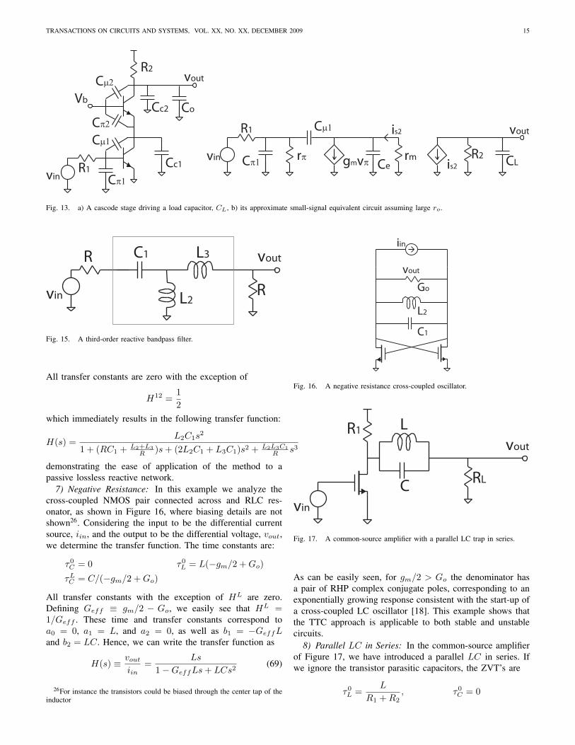
4) Cascode Stage: The cascode stage is illustrated in Figure13a with its small signal equivalent circuit in Figure 13b.We note that for a large transistor output resistance, ro, thetime constants associated with Cπ1, Cµ1, Cc1, and Cπ2 aredecoupled from those of Cµ2, Cc2, and Co, since the time-constant of one group remains unaffected by any combinationof shorting and opening of the other batch. A closer lookalso indicates that capacitors Cc1 = Cjs and Cπ2 are inparallel, so are Cc2 = Cjs, Cµ2, and Co and hence we define,Ce = Cc1 + Cπ2, and CL = Cc2 + Cµ2 + Co and deal withfour capacitors from this point on.
The four ZVT time constants for these capacitors are:
τ0π = Cπ(R1 ‖ rπ)
τ0µ = Cµ[R1 ‖ rπ + αrm + gm(R1 ‖ rπ)αrm]≈ Cµ[2(R1 ‖ rπ) + rm]
τ0e = Ceαrm
τ0L = CLR2
We notice that τ0µ which was the dominant source band-
width reduction in the common emitter of Example VII-1,is now reduced significantly, which explains the well-knownadvantage of the cascode. A numerical calculation of theZVT’s with the same values as the previous examples, predictsωh ≈ 2π ·294MHz, where SPICE simulations indicate a -3dBfrequency of fh = 337MHz.
Noting that τL is decoupled from the other time constants,we can express the transfer function as
H(s) = H0 · 1 + a′1a0
s
(1 + b′1s + b′2s2)· 11 + τLs
R1
vinvoutCπ
CL
Fig. 14. A source follower stage driving a capacitive load, CL.
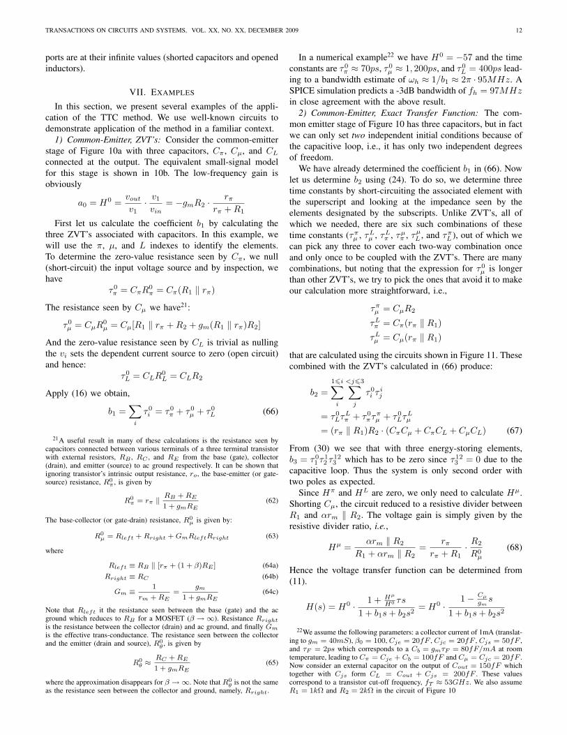
where
b′1 = τ0π + τ0
µ + τ0e
b′2 = αrm(R1 ‖ rπ)(CπCµ + CπCe + CµCe)
and
−1z
=a′1a0
=Hµτ0
µ
H0= −Cµ
gm
thereby determining the transfer function exactly with muchless effort and more insight that nodal analysis.
5) Source Follower with Capacitive Load: Now we con-sider the gain of the source-follower stage with a sourceresistance R1 driving a capacitive load, as shown in Figure14 23. Considering Cπ and CL, the ZVT’s are:
τ0π = rmCπ τ0
L = rmCL
and τLπ is given by
τLπ = R1Cπ
In a numerical example24, we have, b1 = τ0π + τ0
L = 5psand b2 = τ0
LτLπ = 250(ps)2. Using (53) and (55), we obtain,
Q = 3.16 (about 10dB of peaking) and ωn = 2π · 10GHz.The fact that Q is greater than 0.5 clearly indicates that wehave a pair of complex-conjugate poles.
Using (42) we obtain25 an estimate for ωh of 15.9GHz,while the conventional ZVT’s predict ωh = 2π·32GHz, whichis twice as large. A SPICE simulations of this circuit shows10.2dB of peaking at 9.8GHz, with an ωh = 2π ·15.5GHz allvery close to the predictions obtained from our calculations.Note that in practice, this peaking is usually attenuated byCµ and is not as pronounced as shown in this example.Nonetheless, the poles usually remain complex as the Q isoften greater than 0.5.
6) Reactive Bandpass Filter: In this example we applythe approach to determine the exact transfer function of thereactive bandpass network of Figure 15. The time constantsare:
τ01 = RC1 τ0
2 = L2/R τ03 = L3/R
τ12 = 2L2/R τ1
3 = L2/R τ23 = 0
τ123 = L3/2R
23This could be the case if the stage is biased with a current source.24Assuming Cπ = CL = 50fF , gm = 20mS and an R1 = 2kΩ25The only non-zero Hi terms are H0 = 1 and Hπ = 1 leading to
a0 = 1, a1 = rmCπ , and a2 = 0.
TRANSACTIONS ON CIRCUITS AND SYSTEMS, VOL. XX, NO. XX, DECEMBER 2009 15
Cπ1
Cµ1
Cc1
R2
R1vin
vout
Cπ1
Cµ1
CLR2
R1
vin
vout
rπ gmvπ
Co
Cµ2
Cc2
Cπ2
Vb
Cerm
is2
is2
Fig. 13. a) A cascode stage driving a load capacitor, CL, b) its approximate small-signal equivalent circuit assuming large ro.
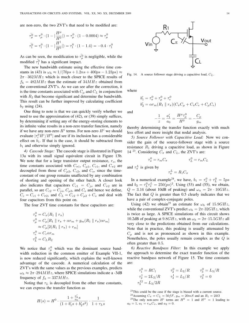
R
vin R
voutL3
L2
C1
Fig. 15. A third-order reactive bandpass filter.
All transfer constants are zero with the exception of
H12 =12
which immediately results in the following transfer function:
H(s) =L2C1s
2
1 + (RC1 + L2+L3R )s + (2L2C1 + L3C1)s2 + L2L3C1
R s3
demonstrating the ease of application of the method to apassive lossless reactive network.
7) Negative Resistance: In this example we analyze thecross-coupled NMOS pair connected across and RLC res-onator, as shown in Figure 16, where biasing details are notshown26. Considering the input to be the differential currentsource, iin, and the output to be the differential voltage, vout,we determine the transfer function. The time constants are:
τ0C = 0 τ0
L = L(−gm/2 + Go)
τLC = C/(−gm/2 + Go)
All transfer constants with the exception of HL are zero.Defining Geff ≡ gm/2 − Go, we easily see that HL =1/Geff . These time and transfer constants correspond toa0 = 0, a1 = L, and a2 = 0, as well as b1 = −GeffLand b2 = LC. Hence, we can write the transfer function as
H(s) ≡ vout
iin=
Ls
1−GeffLs + LCs2(69)
26For instance the transistors could be biased through the center tap of theinductor
Go
L2
vout
C1
iin
Fig. 16. A negative resistance cross-coupled oscillator.
R1
vin
RL
vout
L
C
Fig. 17. A common-source amplifier with a parallel LC trap in series.
As can be easily seen, for gm/2 > Go the denominator hasa pair of RHP complex conjugate poles, corresponding to anexponentially growing response consistent with the start-up ofa cross-coupled LC oscillator [18]. This example shows thatthe TTC approach is applicable to both stable and unstablecircuits.
8) Parallel LC in Series: In the common-source amplifierof Figure 17, we have introduced a parallel LC in series. Ifwe ignore the transistor parasitic capacitors, the ZVT’s are
τ0L =
L
R1 + R2, τ0
C = 0

TRANSACTIONS ON CIRCUITS AND SYSTEMS, VOL. XX, NO. XX, DECEMBER 2009 16
rx
vinvout
Cπ
CL
iin
vinvout
Cπ
CL
iin
a) b)
Fig. 18. a) A source-follower with Cπ driving a load capacitor CL, b) thesame stage with an infinitesimal resistance rx in series with CL.
Since τ0C = 0 and τ0
CτCL = τ0
LτLC according to (26), we can
avoid an indeterminant case27 by calculating τLC = (R1+R2)C
and henceτ0LτL
C = LC
The transfer constants are
H0 = HL = HLC = −gm(R1 ‖ R2)
HL = 0
which result in
H(s) = H0 1 + LCs2
1 + LR1+R2
s + LCs2
where according to (53), we have
Q = (R1 + R2)
√C
L
As can be seen from the transfer function, there is a pair ofimaginary zeros at ±j/
√LC. Since the simultaneously infinite
valued inductor and capacitor result in a non-zero transferfunction, HLC , there are two zeros in the system28.
9) Input Impedance of Source Follower with CapacitiveLoad: Consider the source follower of Figure 18a, driving acapacitive load, CL (considering only Cπ and CL). Calculatingthe input admittance, Y (s), and inverting it is easier sincethe input impedance with both capacitors open is infinite. Tocalculate Y (s) we must drive the input with a voltage source(the stimulus) and take the input current as the output variable,as seen in Figure 18a.
First let us calculate Y 0 when both capacitors are open. Wesimply have:
Y 0 = 0
similarly,
Y π = 0 , Y L = 0
Now consider Y πL. When both Cπ and CL are shorted, ashort is seen looking into the input, and hence Y πL = ∞.While correct this results in an indeterminant case, since forthis configuration τ2
1 = τ12 = 0 which results in a zero times
infinity case for the a2 coefficient. This can be easily resolved
27Since τ0C = 0 and τC
L = L/0, the product is indeterminant. If one insistson using the product τ0
CτCL , it can be determined by placing a resistor rx in
series with L and setting it to zero in the final result.28Note that in this example, a1 is zero while a2 is not, thus the zeros are
a conjugate imaginary pair on the jω-axis.
by introducing a resistance, rx, (which is always there inpractice anyway) in series with the CL (or the input) andsetting it to zero later, as shown in Figure 18b. The previouslycalculated Y 0, Y π, and Y L terms are still zero. The new Y πL
is determined by inspection to be:
Y πL =1rx
Now to find the zero-value time constants, we see byinspection that
τ0π = R0
πCπ = rmCπ
τ0L = R0
LC0 = (rm + rx)CL
and finally we go ahead and calculate τπL as
τπL = Rπ
LCL = rxCL
Using these time-constants and low-frequency transfer func-tions and setting rx → 0, we obtain the input admittance:
Y (s) =rmC1C2s
2
1 + rm(Cπ + CL)s
Note that the above expression has a single pole, because of thearrangement of Figure 18 where Cπ and CL form a capacitiveloop with the voltage source drive nulled (shorted). The aboveexpression can be used to find the input impedance:
Z(s) =1
Y (s)=
gm
CπCLs2+
1(Cπ ‖ CL)s
which is modeled as series combination of a capacitor andwhat is sometimes referred to as a “super capacitor” since ithas a 1/s2 behavior [19][20] More accurately it is a frequencydependent negative resistance (FDNR), as setting s = jω wesee that it presents a negative resistance of
R = − gm
CπCLω2
at the input. This can useful in making oscillators or filters.
VIII. CONCLUSION
The transfer function of circuits can be expressed to the de-sired level of accuracy in terms of time and transfer constantscalculated under different combinations of shorted and openedenergy-storing elements using exclusively low frequency cal-culations. The approach has several useful corollaries in thedesign of analog circuits.
ACKNOWLEDGMENT
The author would like to thank T. Arai, J. Arroyo, A.Babakhani, F. Bohn, S. Bowers, J. Chen, E. Keehr, A. Komi-jani, S. Kosai, S. Mehta, A. Natarajan, K. Sengupta, C. Sidiris,H. Wang, Y.J. Wang, and J. Yoo formerly or currently ofCaltech for valuable feedback on the manuscript. The authoralso acknowledges the anonymous reviewers as well as Prof.B. Murmann of Stanford University and Prof. H. Hashemiof USC for their constructive feedback on the manuscript.Last, but not least, the author is particularly indebted to thestudents in Caltech’s EE114 class who helped improve thismaterial substantially over more than a decade by asking greatquestions and refusing to accept incomplete answers.

TRANSACTIONS ON CIRCUITS AND SYSTEMS, VOL. XX, NO. XX, DECEMBER 2009 17
REFERENCES
[1] H.W. Bode, Network Analysis and Feedback Amplifier Design, VanNostrand, New York, 1945.
[2] E.A. Guillemin, Introductory Circuit Theory, John Wiley and Sons, NewYork, 1953.
[3] J.H. Mulligan, “The Effect of Pole and Zero Locations on the TransientResponse of Linear Dynamic Systems,” Proc. IRE, vol. 37, pp. 516-529,May 1949.
[4] D.O. Pederson and G.H. Wilson, “Dominant Zero and Excess Phase of aHurwitz Polynomial,” IEEE Trans. Circ. Syst., vol. 11, no. 1, pp. 104-108,March 1964.
[5] R.D. Thornton, C.L. Searle, D.O. Pederson, R.B. Adler, E.J. Angelo,Multistage Transistor Circuits, John Wiley and Sons, New York, 1965.
[6] B.L. Cochran, A. Grabel, “A Method for the Determination of the TransferFunction of Electronic Circuits,” IEEE Transactions on Circuit Theory,vol. CT-20, no. 1, pp. 16-20, Jan. 1973.
[7] A.M. Davis, “Analyze Active-Netowrk Responses without Complex Ma-nipulations,” EDN, pp. 109-112, Feb. 1979.
[8] A.M. Davis, E. A. Moustakas, “Decomposition Analysis of ActiveNetworks,” Int. J. Electronics, vol. 46, no. 5, pp. 449-456, 1979.
[9] A.M. Davis, E. A. Moustakas, “Analyze of Active RC Networks byDecomposition,” IEEE Transactions on Circuits and Systems, vol. CAS-27, no. 5, May 1980.
[10] S. Rosenstark, Feedback Amplifier Principles, MacMillan Publishing,New York, 1986.
[11] R.D. Middlebrook, “Null double Injection and the Extra Element Theo-rem,” IEEE Transactions on Education, vol. 32, no. 3, p. 167-180, Aug.1989.
[12] R.M. Fox and S.G. Glee,“Extension of the open-circuit time-constantmethod to allow for transcapacitances,” IEEE Trans. Circuits Syst., vol.37, p. 1167-1171, Sept. 1990.
[13] P. Andreani and S. Mattisson, “Characteristic polynomial and zeropolynomial with the Cochrun-Grabel method,” Int. J. Circ. Theor. Appl.,vol. 26, p. 287-292, May-June 1998.
[14] P. Andreani and S. Mattisson, “Extension of the Cochrun-Grabel Methodto Allow for Mutual Inductances,” IEEE Transactions on Circuits andSystems-I, vol. 46, no. 4, p. 481-483, April 1999.
[15] R.D. Middlebrook, V. Vorperian, and J. Lindal, “The N Extra ElementTheorem,” IEEE Transactions on Circuits and Systems-I, vol. 45, no. 9,p. 919-935, Sept. 1998.
[16] T.H. Lee, The Design of CMOS Radio-Frequency Integrated Circuits,Cambridge University Press, United Kingdom, 1998.
[17] S. Mandegaran and A. Hajimiri, “A Breakdown Voltage Multiplier forHigh Voltage Swing Drivers,” IEEE J. Solid-State Circuits, vol. 42, no.2, p. 302-312, Feb. 2007.
[18] A. Hajimiri and T.H. Lee, “Design Issues in CMOS Differential LCOscillators,” IEEE J. Solid-State Circuits, vol. 34, no. 5, pp. 717-724,May 1999.
[19] L.T. Bruton, “Network Transfer Functions Using the Concept ofFrequency-Dependent Negative Resistance,” IEEE Transactions on Cir-cuit Theory, vol. CT-16, no. 3, pp. 406-408, Aug. 1969.
[20] A. Antoniou,“Realization of Gyrators Using Operational Amplifiers andTheir Use in RC-Active Network Synthesis,” Proc. IEE, vol. 116, pp.1838-1850, 1969.
PLACEPHOTOHERE
Ali Hajimiri Ali Hajimiri received his B.S. degreein Electronics Engineering from the Sharif Univer-sity of Technology, and M.S. and Ph.D. degrees inelectrical engineering from the Stanford Universityin 1996 and 1998, respectively.
He was a Design Engineer with Philips Semicon-ductors, where he worked on a BiCMOS chipset forGSM and cellular units from 1993 to 1994. In 1995,he was with Sun Microsystems, where he workedon the UltraSPARC microprocessor’s cache RAMdesign methodology. During the summer of 1997,
he was with Lucent Technologies (Bell Labs), Murray Hill, NJ, where heinvestigated low-phase-noise integrated oscillators. In 1998, he joined theFaculty of the California Institute of Technology, Pasadena, where he isa Professor of Electrical Engineering and the director of MicroelectronicsLaboratory. His research interests are high-speed and RF integrated circuitsfor applications in sensors, biomedical devices, and communication systems.
Dr. Hajimiri is the author of The Design of Low Noise Oscillators (Boston,MA: Springer, 1999) and has authored and coauthored more than one hundredrefereed journal and conference technical articles. He holds more than twodozen U.S. and European patents. He has served on the Technical ProgramCommittee of the International Solid-State Circuits Conference (ISSCC), asan Associate Editor of the IEEE Journal of Solid-State Circuits (JSSC), asan Associate Editor of IEEE Transactions on Circuits and Systems (TCAS):Part-II, a member of the Technical Program Committees of the InternationalConference on Computer Aided Design (ICCAD), Guest Editor of the IEEETransactions on Microwave Theory and Techniques, and Guest Editorial Boardof Transactions of Institute of Electronics, Information and CommunicationEngineers of Japan (IEICE).
Dr. Hajimiri was selected to the top 100 innovators (TR100) list in 2004and is a Fellow of the Okawa Foundation. He has served as a DistinguishedLecturer of the IEEE Solid-State and Microwave Societies. He is the recipientof Caltech’s Graduate Students Council Teaching and Mentoring award as wellas the Associated Students of Caltech Undergraduate Excellence in TeachingAward. He was the Gold medal winner of the National Physics Competitionand the Bronze Medal winner of the 21st International Physics Olympiad,Groningen, Netherlands. He was a co-recipient of the IEEE Journal of Solid-State circuits Best Paper Award of 2004, the International Solid-State CircuitsConference (ISSCC) Jack Kilby Outstanding Paper Award, a two-time co-recipient of CICC best paper award, and a three-time winner of the IBMfaculty partnership award as well as National Science Foundation CAREERaward. He co-founded Axiom Microdevices Inc. in 2002 which has shippedmore than fifty million fully-integrated CMOS PAs and was acquired bySkywork Inc. in 2009.


![arXiv:1608.03620v1 [physics.optics] 11 Aug 2016copilot.caltech.edu/documents/16931/1608_03620.pdf · Generalized nonreciprocity in an optomechanical circuit via synthetic magnetism](https://static.fdocuments.in/doc/165x107/60445b647eb96b46bc3e962c/arxiv160803620v1-11-aug-2016copilotcaltechedudocuments16931160803620pdf.jpg)