Gateway to.. - KopyKitab · PDF fileGateway to ...PSUs (Synopsis ... (IFFCO). Bhabha Atomic...
16
Transcript of Gateway to.. - KopyKitab · PDF fileGateway to ...PSUs (Synopsis ... (IFFCO). Bhabha Atomic...
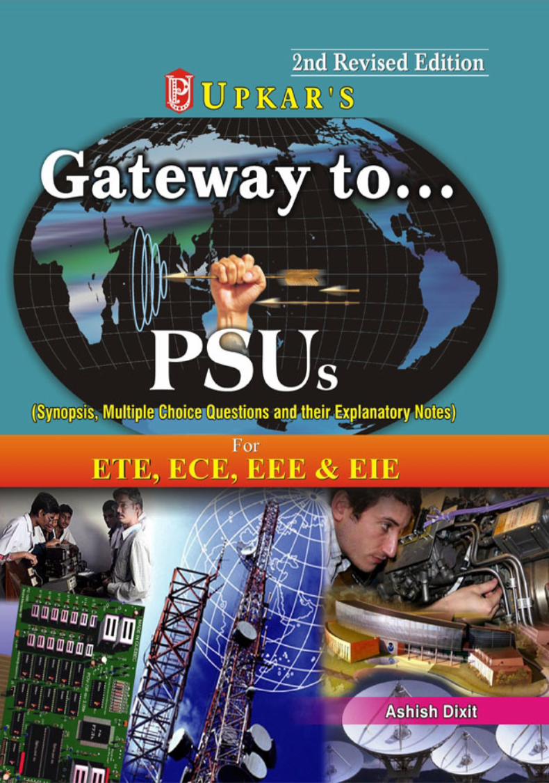

Gateway to...PSUs(Synopsis, Multiple Choice Questions and their Explanatory Notes)
For
Electronics & Telecommunication Engineering (ETE), Electronics &
Communication Engineering (ECE), Electrical & Electronics Engineering (EEE),
Electronics & Instrumentation Engineering (EIE)
By
Upkar Prakashan, AGRA-2
Bharat Electronics Limited (BEL).
Bharat Heavy Electronics Limited (BHEL).
Steel Authority India Limited (SAIL).
Hindustan Aeronautics Limited (HAL).
Indian Oil Corporation Limited (IOCL).
National Thermal Power Corporation Limited (NTPC).
National Fertilizers Limited (NFL).
Centre for Development of Telematics (C-DOT).
Power Grid Corporation of India Limited (PGCIL).
Hindustan Petroleum Corporation Limited (HPCL).
Larsen & Tubro Limited (L & T).
Indian Farmers Fertilizers Corporation Limited (IFFCO).
Bhabha Atomic Research Centre (BARC).
Indian Space Research Organization (ISRO).
Defence Research Development Organization (DRDO), etc.
Useful for
Ashish DixitPhd. Persuing
M.Tech. (V.L.S.I. Design) C-DAC, Mohali (Punjab)
B.Tech. (HONs E & T)
Sr. Lecturer (EC Deptt.)
AMITY UNIVERSITY
Lucknow
Seccond Revised Edition
Printed at : UPKAR PRAKASHAN (Printing Unit) Bye-pass, AGRA
The publishers have taken all possible precautions in publishing this book, yet if any mistake has
crept in, the publishers shall not be responsible for the same.
This book or any part thereof may not be reproduced in any form by Photographic, Mechanical, or
any other method, for any use, without written permission from the Publishers.
Only the courts at Agra shall have the jurisdiction for any legal dispute.
© Authors
Publishers
UPKAR PRAKASHAN(An ISO 9001 : 2000 Company)
2/11A, Swadeshi Bima Nagar, AGRA–282 002
Phone : 4053333, 2530966, 2531101
Fax : (0562) 4053330, 4031570
E-mail : [email protected], Website : www.upkar.in
Branch Offices :4845, Ansari Road, Daryaganj,
New Delhi—110 002
Phone : 011–23251844/66
Pirmohani Chowk,
Kadamkuan,
Patna—800 003
Phone : 0612–2673340
1-8-1/B, R.R. Complex (Near Sundaraiah Park,
Adjacent to Manasa Enclave Gate),
Bagh Lingampally,
Hyderabad—500 044 (A.P.)
Phone : 040–66753330
28, Chowdhury Lane, Shyam
Bazar, Near Metro Station,
Gate No. 4
Kolkata—700004 (W.B.)
Phone : 033–25551510
B-33, Blunt Square, Kanpur Taxi
Stand Lane, Mawaiya,
Lucknow—226 004 (U.P.)
Phone : 0522–4109080
ISBN : 978-81-7482-942-9
Price : 850·00(Rs. Eight Hundred Fifty Only)
Code No. 1657

Heartiest Thanks
To
Mr. Aseem Kumar ChauhanAdditional President
(Ritnand Balved Education Foundation)
AMITY UNIVERSITY
Uttar Pradesh
&
Maj. Gen. K. K. OhriAVSM Retd.
Director General
AMITY UNIVERSITY
Lucknow Campus
Dedicated to
GrandfatherGrandfatherGrandfatherGrandfatherGrandfather
Late Mr. Ram Prasad DixitLate Mr. Ram Prasad DixitLate Mr. Ram Prasad DixitLate Mr. Ram Prasad DixitLate Mr. Ram Prasad Dixit
FatherFatherFatherFatherFather
Mr. Uidya Dhar DixitMr. Uidya Dhar DixitMr. Uidya Dhar DixitMr. Uidya Dhar DixitMr. Uidya Dhar Dixit
&&&&&
MotherMotherMotherMotherMother
Smt. Mithlesh DixitSmt. Mithlesh DixitSmt. Mithlesh DixitSmt. Mithlesh DixitSmt. Mithlesh Dixit
PREFACEPREFACEPREFACEPREFACEPREFACE
It is a matter of great pleasure to present this book ‘‘Gateway to… PSUs’’. Getting a job in the PSUs like BSNL & VSNLand other PSUs like, DRDO, ISRO, NTPC, GAIL, BHEL, BARC, NHPC, SAIL, IOCL etc. has always been an aspiration of engineeringgraduates. Although a number of books are available for entrance examinations for these jobs, the present book makes a significant
departure from its predecessors because of its encyclopaedic subject matter and its innovative and lucid presentation. I am surethat this book will provide complete satisfaction to the readers. Presently the market scenario is confusing and it is hard to find theoptimum quality books. While preparing this manuscript, I continuously kept in mind the requirements of the aspirants regarding
the latest trends of these entrance examinations as well as the most intricate concepts involved.
This book is divided into twenty units. Each unit begins with a synopsis and ends with multiple choice questions and theirexplanatory notes. The variety and quality of problems also makes this book unique and an asset for the aforementioned
examinations.
Salient Features of the Book Synopsis has been given in the beginning of each topic for a quick and easy review just before the examination.
More than 4500 objective solved problems.
Special tricks are given to solve the objective problems in order to save the time during examination.
It covers many objective problems frequently asked in various competitive examinations.
For a better understanding many problems have been solved graphically.
Previous years question papers fully solved.
This work has come into being only because of the unparallel help and support that came from Mr. Ankit Singh, Mr. AnkitJain, Mr. Mayank Srivastava, Mr. Kranti Kumar, Mr. Dheeraj Shukla, Mr. Pawan Kumar Saini. Their contribution to this work is
second to none.
No words are sufficient to express my gratitude to Sri Vidya Dhar Dixit, Avatar Singh, Mrs. Mithlesh Dixit, Mr. RadhesyamDixit, Mr. Prakash Dixit, Paramjit Kaur, Uday Shanker Trivedi, Anita Trivedi, Archana and Amita, Sukhwinder Kaur, Jasvinder Kaur
and elder brother Suresh Kumar Tripathi and wife Annapurna, for their cooperation, patience and support during the preparationof the manuscript.
We would like to thank all our friends like Akhilesh Shukla, Satish Shukla, Ankit Kumar Singh, Dheeraj Shukla, Mayank
Srivastava, Pawan Saini, Sarika Mishra, Abhishek Dwivedi, Anand Singh Chauhan, Rohit Singh, Rajeev Singh, Ganga Raju,Talvinder Kaur, Umesh Pandey Mrs. Mehga Singhla and Shivendra Singh Chauhan for their encouragement during the preparationof the book.
We would also like to thank all our parents like Mr. Mohan Chandra Tripathi, Mr. Nageswar Nath Upadhyay (IAS General-Secretary) Mr. Shankari Singh Chauhan, Mr. Surya Kumar Tripathi, Mr. Ram Sevak Singh Chauhan, Mr. Lallan Mishra, Mr. BindadinSingh Chauhan, Mr. Santa Kumar Dixit, Mr. Ram Gopal Singh Chauhan, Mr. Suresh Kumar Tripathi, Mr. Dev Chaitanya Brahmachari,
Mr. Om Prakash Yadav, Dinesh Jaiswal, Sanjay Dixit, Mohd. Irsad Khan (MLA Sarojininagar Lucknow) .
I wish to express my gratitude to Mr. Mahendra Jain, Upkar Prakashan, Agra, for publishing this manuscript.
Suggestions for the improvement of this book will be greatly acknowledged and incorporated in the nextedition.
—Ashish Dixit
ACKNOWLEDGMENTACKNOWLEDGMENTACKNOWLEDGMENTACKNOWLEDGMENTACKNOWLEDGMENT
I am very much grateful to a number of colleagues who have given us enormous contributions and cooperation during the
preparation of the manuscipt of this book. I would like to give my hearty thanks to the following persons for their continuous
support, encouragement throughout this book, like........
Prof. S. K. Jha (CEST, Lucknow), Prof. Anuj Goel (H.O.D. EC B. N. Institute, Lucknow, Miss Shrushut (CEST Lucknow), Mr.
B. K. Chauhan (N.I.E.C. Lucknow), Mrs. Indu Prabha Singh (H.O.D. EC S.I.T.M., Unnao, Mr. Sameer Srivastava (S.I.T.M. Barabanki),
Mr. Rahul Mishra (Dr. M.C. Saxena, Lucknow), Dr. Manish Gupta, AMITY UNIVERSITY, Lucknow, Mr. Marut Tiwari, Mr. Prabhaker
Dubey, N. I. E. C., Lucknow. Mr. Gurumohan Singh & Mrs. Shivani Wadhwa, Mr. H.S. Sagar Director, SBBSIET, Jalandhar, Dr.
Arun Khosla, Dr. B.R. Sood Professor, SBBSIET, Jalandhar, Mr. Kamaljit Singh Professor, NIT, Jalandhar, Dr. Sukhbeer Bindra
Professor GNDN, Amritsar, Mr. Neeraj Sharma Senior Lecturer VIET, Chandigarh, Mr. Mandeep Singh Engineer BEL, Ghaziabad,
Dr. M.L. Singla Scientist F, Deputy Director CSIO, Punjab, Mr. Manish Gupta, Mr. Kidwai Siddique, H.O.D. Electronics AIET,
Lucknow, Mr. Anand Chopra , Mr. Bhabhaya Alankar Lecturer, N.I.T. Jalandhar, Mr. Ankit Kumar Senior Lecturer, AIET Lucknow,
Mr. Sanjay Jain Indian Engineering Services, Mr. Abhishek Agrahari Design Engineer N.I.T. Surat, Mr. Bijendra Saini, (IES), Mrs.
Lalita Sharma Senior Lecturer, I.E.T. Khandari, Agra, Mr. Yogendra Kumar Prajapati Senior Lecturer, V.I.E.T. Bijnour, Mr. Puneet
Chandra Srivastava, Associate Professor R.K.G.I.T. Ghaziabad, Mr. Vivek Srivastava Senior Lecturer, N.I.E.T. Greater Noida, Mr.
Sanjay Singh GAIL, India, Miss Aplana Sharma, Dr. P.K. Pandey (H.O.D. EC MPGI, Lucknow), Mr. Pawan Yadav, Mr. C.K. Dixit,
Mr. Ravi Kant, Mr. Satendra Yadav HOD EC Deptt., B.B.I.E.T. Bulandsahar, Mr. Rafeek Ahmad, Mr. Vinod Kumar Yadav and
Miss Smriti Agrawal.
I would like to express my special thanks to Mr. Ambika Misra, Secretary Ambalika Institute of Management & Technology
Lucknow, Dr. S. Q. Abbas, Director, Ambalika Institute of Management and Technology, Lucknow, Dr. Alok Kumar Mishra, Additional
Director Ambalika Institute of Management and Technology, Mr. Sunil Kumar, Dean Academic, Ambalika Institute of Management
and Technology, Lucknow, Mr. U. P. Singh, Dr. Mansi Mishra, Mr. Sandeep Dwivedi, Mr. Ravi Kumar Tiwari, Mr. Sonu Kumar Rai,
Miss Anuradha Yadav, Miss Sabika Ahmad, Miss Monika & Prof. Karmakar all from Ambalika Institute of Management and
Technology, Lucknow.
I would also like to express my special thanks Maj Gen. K.K. Ohri, Prof. S.T.H. Abidi, Prof. N.R. Yadav, Dr. O.P. Singh, Mr.
Arun Pathak, Dr. Neetu Agrawal, Mrs. Gitika Srivastawa, Miss Sarika Mishra, Mr. Zia Abbas, Mr. Anupam, Mr. Sachin Kumar, Mr.
Yashu Swami, Dr. Amit kumar Mishra, Mr. Anirudh Banergi, Mr. Sienu Rizavi, Mr. Loknath Mishra, Mr. Rajinder Tiwari, Dr. Nidhi
Mathur, Miss Shilpi Bisth and Mr. Sudhir Pandey AMITY UNIVERSITY Lucknow Campus.
— Ashish Dixit

CONTENTSCONTENTSCONTENTSCONTENTSCONTENTS
1. Network & Systems 1–136 Objective Problems on Switching……………………………………………………………………………… 28 Answers with Explanatory Notes………………………………………………………………………….…… 30 Objective Problems : Level 1…………………………………………………………………………………... 34 Answers with Explanatory Notes………………………………………………………………………….…… 62 Objective Problems : Level 2…………………………………………………………………………………... 105 Answers with Explanatory Notes………………………………………………………………………….…… 116
2. Electronics Devices 1–96 Objective Problems……………………………………………………………………………………………… 28 Answers with Explanatory Notes………………………………………………………………….…………… 51 Miscellaneous Problems…………………………………………………………………………………….….. 74 Answers with Explanatory Notes…………………………………………………………………………….… 88
3. Analog Circuits 1–88 Objective Problems……………………………………………………………………………………………… 39 Answers with Explanatory Notes…………………………………………………………………………….… 64
4. Digital Circuits 1–56 Objective Problems : Level 1…………………………………………………………………………………... 28 Answers………………………………………………………………………………………..…………………. 33 Objective Problems : Level 2
(i) Problems of Boolean Theorems and Logic Gates………………………………………………………… 34 Answers with Explanatory Notes…………………………………………………………………………….… 37
(ii) Problems on Combinational Logic Circuits……………………………………………………………….. 41 Answers with Explanatory Notes…………………………………………………………………………….… 43
(iii) Problems on Sequential Circuits : Flip-Flop……………………………………………………………… 45 Answers with Explanatory Notes…………………………………………………………………………….… 48
(iv) Problems on Counter…………………………………………………………………………………...….. 49 Answers with Explanatory Notes………………………………………………………………………….…… 52
(v) Problems on Register…………………………………………………………………………………...…... 52 Answers ………………………………………………………………………………………..………………... 53
(vi) Problems on Memory Organisation……………………………………………………………………….. 53 Answers with Explanatory Notes…………………………………………………………………………….… 55
5. Microprocessor 1–64 Objective Problems : Level 1…………………………………………………………………………………... 16 Answers with Explanatory Notes………………………………………………………..……………………... 23 Short Answer Type Questions………………………………………………………………………………….. 26 Miscellaneous Problems on Digital Circuits & Microprocessor…………………………………………….. 27 Answers with Explanatory Notes………………………………………………………………………….…… 47
6. Signals & Systems 1–112 Objective Problems……………………………………………………………………………………………… 45 Answers with Explanatory Notes…………………………………………………………………………….… 71
7. Control Systems 1–76 Objective Problems……………………………………………………………………………………………… 24 Answers with Explanatory Notes………………………………………………………………………………. 47
8. Communications 1–56 Objective Problems : Level 1…………………………………………………………………………………... 25 Answers with Explanatory Notes………………………………………………………………………………. 28

( xii )
Objective Problems : Level 2…………………………………………………………………………………… 29 Answers with Explanatory Notes………………………………………………………………………………. 35 Objective Problems : Level 3…………………………………………………………………………………… 36 Answers with Explanatory Notes………………………………………………………………………………. 47
9. Electromagnetics 1–60 Objective Problems : Level 1…………………………………………………………………………………… 23 Answers with Explanatory Notes………………………………………………………………………………. 26 Objective Problems : Level 2…………………………………………………………………………………… 27 Answers with Explanatory Notes………………………………………………………………………………. 42
10.Power Electronics 1–51 Objective Problems : Level 1…………………………………………………………………………………… 35 Answers………………………………………………………………………………………..…………………. 40 Objective Problems : Level 2…………………………………………………………………………………… 41 Answers………………………………………………………………………………………..…………………. 51
11. Microwave Engineering 1–31 Objective Problems : Level 1…………………………………………………………………………………… 19 Answers………………………………………………………………………………………..…………………. 26 Objective Problems : Level 2…………………………………………………………………………………… 27 Answers with Explanatory Notes………………………………………………………………………….…… 31
12.Optical Fibre Communication 1–16 Objective Problems……………………………………………………………………………………………… 5 Answers with Explanatory Notes………………………………………………………………………………. 12
13.Electrical Engineering Materials 1–39 Objective Problems……………………………………………………………………………………………… 15 Answers with Explanatory Notes………………………………………………………………………………. 33
14.Measuring Instruments 1–44 Objective Problems……………………………………………………………………………………………… 23 Answers with Explanatory Notes………………………………………………………………………………. 36
15.Satellite Communication 1–24 Objective Problems……………………………………………………………………………………………… 13 Answers with Explanatory Notes………………………………………………………………………………. 22
16.Radar Engineering 1–11 Objective Problems……………………………………………………………………………………………… 6 Answers with Explanatory Notes………………………………………………………………………………. 9
17.Television 1–16 Objective Problems……………………………………………………………………………………………… 6 Answers with Explanatory Notes………………………………………………………………………………. 16
18.Computer Engineering 1–1619.Dictionary of Electronics 1–1620.General Ability Test 1–31 Model Question Papers 1–92 Practice Paper - 1…………………………………………………………………………………..…………… 3 Answer with Hints…………………………………………………………………………………...…………… 12 Practice Paper - 2…………………………………………………………………………………..……………. 23 Answer with Hints…………………………………………………………………………………..……………. 32 Practice Paper - 3…………………………………………………………………………………...…………… 49 Answer with Hints…………………………………………………………………………………...…………… 57 Practice Paper - 4…………………………………………………………………………………...…………… 67 Answer with Hints…………………………………………………………………………………...…………… 78

Network and Systems

NNNNEEEETTTTWWWWOOOORRRRKKKK AAAANNNNDDDD SSSSYYYYSSSSTTTTEEEEMMMMSSSS Kirchhoff Voltage Law (KVL) is a consequence of the
law of conservation of energy, voltage being the energy(or work) per unit charge.
Kirchhoff Current Law (KCL) is the consequence ofconservation of charge. Since the algebraic summationof the charge must be zero, the time derivative of thissummation must also equal to zero.
Star to Delta Transformation
A
B C
RA
RB RC
A
B C
RAB RCA
RBC
O
RAB
=RA RB + RB RC + RC RA
RC
or RAB
= RA + R
B +
RA RBRC
Similarly,
RBC
=RB RC + RC RA + RA RB
RA
and RCA
=RC RA + RA RB + RB RC
RB
Delta to Star Transformation
A
B C
RA
RB RC
A
B C
RAB RCA
RBC
O
RA
=RAB × RAC
RAB + RBC + RCA
Similarly, RB
=RAB × RBC
RAB + RBC + RCA
and RC
=RAC × RBC
RAB + RBC + RCA
Resistance of a wire depends on its material and itssize. It is given by
R =ρlA
where, ρ = Resistivity of a material in Ω cm
l = Length of the wire, andA = Area of cross-section of wire.
Self inductance (L) is the property of conductor (orcoil) by virtue of which it opposes any change indirection or magnitude of current flowing through itself.It is given by
L = Nφl henry
where, N = No. of turns in the coil
φ = Flux set by current I.
Also, L = µ0 ur N2A
l henry
Current through inductor is given by
i (t) = 1L ∫
t
–∞ V dt or 1L ∫
t
–∞ V dt + i(0) amp
Voltage across inductor is given by
V = L didt = N
dφdt volt
Power, P = VI = LI didt watt
When n inductors are connected in series the equiva-lent inductance is
Leq
= L1 + L
2 + L
3 + .....+ L
n
When n inductors are connected in parallel the equiva-lent inductance,
1L
eq=
1L
1 +
1L
2 +
1L
3 + ..... +
1L
n
Relation between the mutual inductance and two coilswith inductance L
1 and L
2 is given by relation.
M = k √L1L2 where 0 ≤ k ≤ 1
where k = coefficient of coupling. It is a measure ofamount of linking flux produced by one coil, w.r.t. othercoil.
Capacitance is the property of material by virtue ofwhich it opposes the variation in potential between thetwo sides
C =qV
where, q = charge, V = potential
C =ε0 εrA
d

4 | NETWORK AND SYSTEMS
where C = Capacitance is proportional to the dielectricand area of the plates, and is inversely proportional tothe distance between the plates.
ε0
= 8.86 × 10– 12 F/m
εr
= Relative permittivity
A = Area of the plate
d = Spacing between two plates.
Current through the capacitor is
i = C dvdt Amp.
Voltage across the capacitor is
V = 1C ∫
t
–∞ i (t) dt or 1C ∫
t
–∞ i(t) dt + VC
(0)
where VC
(0) = initial voltage on capacitor.
When n capacitances are connected in series, theequivalent capacitance is given by
1
Ceq
=1C
1 +
1C
2 +
1C
3 + ..... +
1C
n
When n capacitances are connected in parallel, theequivalent capacitance is given by
Ceq
= C1 + C
2 + C
3 + ..... + C
n
Some conservation laws are given below :
(a) The conservation of charge
q1 = q
2 and C
1 V
1 = C
2 V
2 ; i ≠ ∞
(b) The conservation of flux linkage
ψ1 = ψ
2 and L
1 i
1 = L
2 i
2 ; v ≠ ∞
(c) The conservation of momentum
P1 = P
2 and m
1 v
1 = m
2 v
2 ; F ≠ ∞
Mutual Inductance (M)
It is the ability of one coil to produce an inducedvoltage in a nearby coil by electromagnetic induction,when the current being changed in the first coil, theaction is vice-versa. It is measured in terms of thecoefficient of mutual induction.
GRAPH THEORY
Network topology is only concern with the geometricalstructure of the network.
A graph of any Network can be drawn by placing all thenodes which are points of intersection of more than twobranches. Consider a network given below :
R1 R2 R3
C1 C21
23
4
L
12
3
4
Given network Graph of the given network
If there exists a path between every pairs of nodes of agraph, then the graph is said to be a connected graph.
There are at least two branches in a circuit.
Rank of graph = n –1, where n = no. of nodes orvertices.
A subgraph is a subset of the branches and nodes of agraph. The subgraph is said to be proper if it consistsof strictly have branches and nodes less than all thebranches and nodes of the graph.
Any tree contains n – 1 branches where n is thenumber of nodes or vertices. The branches in a treecalled twig the branches other than the twig is calledlink (also called cords).
12
3
4
1
23
4 65
Correspondingtree
1 2 3
5
23
4
Given graph Tree
Fig. : Simple graph and Tree
In the above figure branches 3, 2, 5 are called twigwhile the branches 1, 4, 6 called link.
Properties of Trees
(i) In a tree, there exist one and only one pathbetween any pair of nodes.
(ii) Every connected graph has at least one tree.
(iii) All the links of a tree together constitute thecomplement of the corresponding tree is calledco-tree.
(iv) Each tree has (n – 1) branches.
(v) The rank of tree is (n – 1). This is also the rank ofa graph to which the tree belongs i.e., both treeand graph has some rank. Where n is the numberof nodes in a graph.
(vi) No. of possible trees of a graph = dct [[A] [AT]]where A is the reduced incidence matrix.
If the total number of branches and nodes in a connec-ted graph are b and n respectively, then the number oflinks l is given by
l = b – n + 1
Incidence Matrix
Tells information about the branches connected atwhich nodes and what the orientations relative tonodes. It is denoted by A
a.
The matrix obtained from Incidence Matrix (Aa) by elimi-
nating one of the rows is called the reduced incidencematrix denoted by A. It is of order (n – 1)a × b
where, n = No. of nodesb = Branches
Properties of Complete Incidence Matrix :
(i) Sum of entries in any column is zero.
(ii) The determinant of the complete incidence matrix ofa closed loop is zero.

NETWORK AND SYSTEMS | 5
Fundamental circuit or tie set matrix can be obtainedby taking one link and other twigs at a time. The num-ber of fundamental circuit depends upon the number oflink.
Consider a graph given below and select a tree.
1 23
4
1
24
6
5
12
3
4
3
Given graph Corresponding tree
Fundamental loops = b – n + 1 = No. of link
Number of twig = n – 1
where, n = No. of nodes
b = No. of branches
The fundamental circuit can be drawn as :
1 2 3
4
1
5 4loop1
1 2 3
4
2
34
loop2
loop 31 2
6
1 2 3
4
In matrix form :
fundamental Branches
circuit 1 2 3 4 5 6
5 1 0 0 –1 1 0
3 0 1 1 1 0 0
6 1 1 0 0 0 1
Cut-set matrix is formed by taking one twig and allother link. The set of branches which is cut by theclosed line forms a cut set.
Cut set separates the node of the given graph into twographs.
The no. of cut-set is equal to the no. of nodes.
Cut-set containing only one twig are independent andare known as fundamental cut sets (f-cut sets)
Number of cut-sets = Number of twig = n – 1
where n = No. of nodes in a graph.
Consider a graph having 5 nodes shown below :
1 3
2
4
5
a
b c
d
e
f
g
h
1 3
2
4
5
Given graph Corresponding tree
3
4
1
2
5
C4
C2
C3C1
a
bc
d
e
f
g
h
Fig. : Formation of cut-set
Since in the given graph there are 5 nodes, so 5 – 1= 4 cut-sets are possible. One thing should be kept inmind that the orientation of a cut-set is decided by thedefining branch of the tree.
Line four cut sets for the above choice of the tree are(a, c, b) ; (b, f, c) ; (c, g, d) ; (d, h, a) and each cut setdefines a cut-set row vector. The cut-set (a, e, b), forexample, defines the following cut-set row vector.
Network shown below :
Z1 Z2
Z3
T-Network
Z1 Z2
Z3
π-Network
Z2 Z4
Z1
Ladder Network
Z3 Z5
Z6
Z1
Bridge Network
Z2
Z3
Z4
Note : These network are said to be grounded or un-balanced network.
Planar graph : It is possible to draw a graph on sheetof paper without crossing the lines then such types ofthe graph are said to be planar graph. Some of theplanar graph is shown below :
a
b
c
d
b
c
d
a
Non-planar graph : If graph is drawn with crossinglines then it is called non-planar graph. Fig. shows thenon-planar graph.
(i) Non-planar graph (ii) Non-planar graph

6 | NETWORK AND SYSTEMS
COUPLING
Dot notation : Dot on the coils indicate the polarity ofvoltages induced in the coils. These also indicatewhether the fluxes produced by the coils will be additiveor opposing.
(i) When coils are joined in series with fluxes additive,the equivalent inductance is
Leq
= L1 + L
2 + 2M
M
L1 L2
Leq
= L1 + L
2 – 2M (for opposing fluxes) →
M
L1 L2
Coefficient of coupling : The amount of couplingbetween the inductively coupled coils is expressed interms of the coefficient of coupling, which is defined as
K = M
√L1 L2
where, M = mutual inductance between the coils
L1 = Self inductance of the first coil
L2 = Self inductance of the second coil
Coefficient of coupling, K is always less than unity.
Maximum value of 1 or 100% called perfect coupl-ing, when the entire flux of one coil links the other.
The greater the coefficient of coupling between thetwo coils, the greater the mutual inductance bet-ween them and vice versa.
K is a non negative number and is independent ofthe reference directions of the currents in thecoils.
If the two coils are a great distance apart in space,the mutual inductance in very small and k is alsovery small.
K ≈ 0.99 → Iron-core coupled circuits
K varies between 0.4 to 0.8 for air core coupledcircuits.
M ≤ √L1 L2 (GATE 2001)
For better understanding the concept of the dotnotation we must know the types of Coupling.
Types of Coupling :
(i) Electrical Coupling : Two coils are connected by awire, so that physical connection exists.
(ii) Magnetic Coupling : Two coils are magneticallycoupled but physically isolated, so called trans-former coupling.
(i) Magnetic Coupling : Consider two inductors withself inductances L
1 and L
2, mutual inductance M,
and coefficient of coupling K and dots are shown infig. applying KVL to both side we get
L1
i ( t)1
R1V (t)1
+
–
i (t)1
i ( t)1
L2 R2
M
M = K √L1 L2
where, 0 ≤ K ≤ 1
V1 (t) = L
1
di1(t)dt + M
di2(t)dt + R
1 i
1 (t),
and L2
di2(t)dt + M
di1(t)dt + R
2 i
2 (t) = 0
A transformer replaced by its T-equivalent :
Magnetic adding :
L1V1
+
–
i1
M
+
–
i2L2 V2
+
–
i1V1
L1 –M L2 –M
i2
M L2
+
–
Magnetic opposition :
L1V1
+
–
i1
M
+
–
i2L2 V2
+
–
i1V1
L1+M L2+M
i2
–M L2
+
–
(ii) Electrical Coupling :Case 1 : When Coupled inductors in series :
M
L1
L2
LeqM
L1
L2
Leq
= L1 + L
2 + 2M
M
L1
L2
LeqM
L1
L2
Leq
= L1 + L
2 – 2M
Case 2 : Coupled inductors in parallel :M
L2Leq L1
M
L2L1

NETWORK AND SYSTEMS | 7
Leq
= L1 L2 – M2
L1 + L2 – 2M
M
L2Leq L1
M
L2L1
Leq
= L1 L2 – M2
L1 + L2 + 2M
Case 3 :
L1 L2
M
Leq
or
M
Leq
Leq
= L1 – M2
L2
L1 L2
M
Leq
L3
Leq
= L1 – M2
L2 + L3
→Transformer as an impedance matching device :
+
–
V1
1
ZinV2
2
+
–N : N
I : nl1 l2
ZL
Zin
= V1I1
=
1n V2
– I2 n
and V2
V1 =
N2N1
= n = I1I2
and Zin
= ZL
n2
PHASORS AND PHASOR DIAGRAMS : Phasor is a directed line segment, whose magnitude is
the maximum value of the cosine function and angle isthe initial phase of the cosine function.
Phasor can be treated as complex number. When thecircuit is analyzed using phasors, it is said to be in thefrequency domain.
There are three equivalent notations for a phasor.
Polar form V = Vm
∠θRectangular form V = V
m (cos θ + j sin θ)
Exponential form V = Vm
ejθ
The cosine function can be written from the givenPhasor.
V (t) = Re [V ejωt ]
= Re [V
m ejθ . ejωt ]
= Re [V
m ej (ωt + θ)]
V (t) = Vm
cos (ωt + θ).
Both polar and exponential forms are used for the multi-plication or division of two phasors, whereas rectan-gular form is used for addition and subtraction of twoPhasors.
Phasor Diagrams :
RL Series Circuit :
+
–~
+ –VR
RI
L +
–VLV
VR
Vθ
VL
I
VR
V = √V2R + V2
L
θ = tan– 1 (VL/V
R)
Power factor = cos θ (lagging)
RC Series Circuit :
θ+
–~
+ –VR
RI
C +
–VCV
VR
V
VC
I
V = √V2R + V2
C
θ = tan– 1 (VC
/VR
)
Power factor = cos θ (leading)
RLC Series Circuit :
+
–~
+ –VR
RI C
+
–VCV
+ –VL
For VL > V
C :
θ
VL
(V –V )L C
VR
VC
V
I

Gateway to PSUs (Electronics &Telecom, Electronics &
Communication, Electrical, Electronics& Instrumentation)
Publisher : Upkar Prakashan ISBN : 9788174829429 Author : Ashish Dixit
Type the URL : http://www.kopykitab.com/product/10399
Get this eBook
30%OFF