Gates - dspace.mit.edudspace.mit.edu/.../CF14DC5A-D4E5-4AA7-B8E2-EEE766B28A61/0/L04Gates.pdf6.004 -...
24
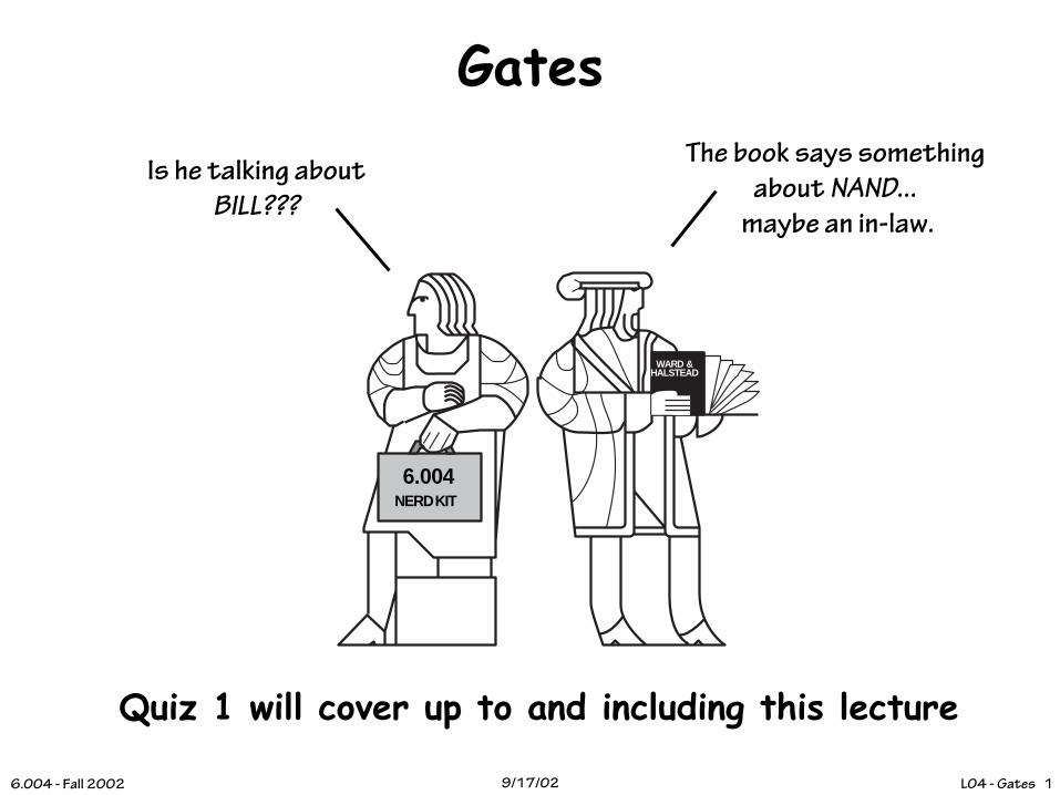
L04 - Gates 1 6.004 - Fall 2002 9/17/02 Gates Quiz 1 will cover up to and including this lecture The book says something about NAND... maybe an in-law. WARD & HALSTEAD NERD KIT 6.004 Is he talking about BILL???
Transcript of Gates - dspace.mit.edudspace.mit.edu/.../CF14DC5A-D4E5-4AA7-B8E2-EEE766B28A61/0/L04Gates.pdf6.004 -...
L04 - Gates 16.004 - Fall 2002 9/17/02
Gates
Quiz 1 will cover up to and including this lecture
The book says something
about NAND...
maybe an in-law.
WARD &HALSTEAD
NERD KIT6.004
Is he talking about
BILL???

L04 - Gates 26.004 - Fall 2002 9/17/02
A Quick Review• A combinational device is a circuit element that has
– one or more digital inputs
– one or more digital outputs
– a functional specification that details the value of each output for
every possible combination of valid input values
– a timing specification consisting (at minimum) of an upper bound
tPD on the required time for the device to compute the specified
output values from an arbitrary set of stable, valid input values
Staticdiscipline
If C is 1 then copy A to Y,otherwise copy B to Y
I will generate a validoutput in no more than
2 weeks after seeing valid inputs
input A
input B
input C
output Y

L04 - Gates 36.004 - Fall 2002 9/17/02
VTC and the Static Discipline
Vil
Vol
Vih
Voh
Vout
Vin
Vol Vil Vih Voh
Static Discipline requires that we avoid gray areas, which correspond to valid
inputs but invalid outputs. Net result: combinational devices must have GAIN
and be NONLINEAR.
The good news: CMOS gates do all this with the added bonus of no static
power!
Inverting gates Non-inverting gates

L04 - Gates 46.004 - Fall 2002 9/17/02
Due to unavoidable delays…Propagation delay (tPD):
An UPPER BOUND on the delay from valid inputs to valid outputs.
GOAL:minimizepropagationdelay!
ISSUE:keep Capacitanceslow andtransistorsfast
VOUT < tPD< tPD
VIN
VOL
VOH
VIL
VIH
time constant τ = RPD•CL
time constant τ = RPU•CL

L04 - Gates 56.004 - Fall 2002 9/17/02
Contamination Delayan optional, additional timing spec
INVALID inputs take time to propagate, too...
CONTAMINATION DELAY, tCD
A LOWER BOUND on the delay from any invalid input to an invalid output
VOUT > tCD> tCD
VIN
VOL
VOH
VIL
VIH
Do we really need tCD?
Usually not… it’ll be
important when we
design circuits with
registers (coming
soon!)
If tCD is not specified,
safe to assume it’s 0.
Do we really need tCD?
Usually not… it’ll be
important when we
design circuits with
registers (coming
soon!)
If tCD is not specified,
safe to assume it’s 0.

L04 - Gates 66.004 - Fall 2002 9/17/02
The Combinational Contract
A BA B
0 11 0
tPD propagation delaytCD contamination delay
A
B
Must be ___________
Must be ___________
Note:1. No Promises during 2. Default (conservative) spec: tCD = 0
< tPD
> tCD

L04 - Gates 76.004 - Fall 2002 9/17/02
Example: Timing Analysis
If NAND gates have a tPD = 4nS and tCD = 1nS
B
C
A
Y
tPD = _______ nS
tCD = _______ nS
12
2
tPD is the maximum cumulative
propagation delay over all paths
from inputs to outputs
tCD is the minimum cumulative
contamination delay over all
paths from inputs to outputs
L04 - Gates 86.004 - Fall 2002 9/17/02
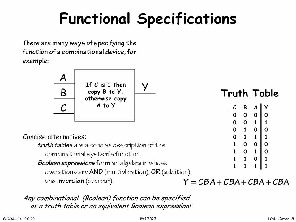
Functional SpecificationsThere are many ways of specifying the
function of a combinational device, for
example:
AB YIf C is 1 then
copy B to Y,otherwise copy
A to YC
Concise alternatives:truth tables are a concise description of the
combinational system’s function. Boolean expressions form an algebra in whose
operations are AND (multiplication), OR (addition), and inversion (overbar).
Any combinational (Boolean) function can be specified as a truth table or an equivalent Boolean expression!
C B A Y0 0 0 00 0 1 10 1 0 00 1 1 11 0 0 01 0 1 01 1 0 11 1 1 1
Truth Table
CBAACBBACABCY +++=

L04 - Gates 96.004 - Fall 2002 9/17/02
Oh yeah… one last issue
Recall the rules for combinational devices:
Output guaranteed to be valid when all inputs have been
valid for at least tPD, and, outputs may become invalid no
earlier than tCD after an input changes!
Many gate implementations--e.g., CMOS—
adhere to even tighter restrictions.
A
B
ZtPD
tCD
AZB
A
B
ZtPD
tCD
0
0
1
1
0
1
0
1
1
0
0
0
A B Z
NOR:

L04 - Gates 106.004 - Fall 2002 9/17/02
What happens in this case?
LENIENT Combinational Device:Output guaranteed to be valid when any combination of inputs
sufficient to determine output value has been valid for at least tPD.
Tolerates transitions -- and invalid levels -- on irrelevant inputs!
A
B
ZtPD
tCD
Input A alone is sufficient to determine the output
A
B
Z
A
B
Z
0
X
1
0
1
X
1
0
0
A B Z
0
0
1
1
0
1
0
1
1
0
0
0
A B ZNOR: Lenient
NOR:

L04 - Gates 116.004 - Fall 2002 9/17/02
Lets design stuff!Where do we start?
A
B
6.004Gates
F = A xor B
We can build ANY
Combinational Device…
can’t we????
We have a bag of gates.
We have a spec.
What do we do?
Did I mention we
have gates?
We need
… a systematic approach for
designing logic

L04 - Gates 126.004 - Fall 2002 9/17/02
A Slight DiversionAre we sure we have all the gates we need?
Just how many two-input gates are there?
Hum… all of these have 2-inputs (no surprise)
… each with 4 combinations, giving 22 output cases
How many ways are there of assigning 4 outputs? ___
AB Y00 001 010 011 1
ANDAB Y00 001 110 111 1
ORAB Y00 101 110 111 0
NANDAB Y00 101 010 011 0
NOR
2 = 24 = 1622

L04 - Gates 136.004 - Fall 2002 9/17/02
There are only so many gates
There are only 16 possible 2-input gates
… some we know already, others are just silly
Do we need all of these gates?
I N P U T AB
Z E R O
A N D
A>B
A
B>A
B
X O R
O R
N O R
X N O R
N O T ‘B’
A<=B
N O T ‘A’
B<=A
N A N D
O N E
00 0 0 0 0 0 0 0 0 1 1 1 1 1 1 1 1 01 0 0 0 0 1 1 1 1 0 0 0 0 1 1 1 1 10 0 0 1 1 0 0 1 1 0 0 1 1 0 0 1 1 11 0 1 0 1 0 1 0 1 0 1 0 1 0 1 0 1
Nope. After all, we describe them all using AND, OR, and NOT.
How many of
these gates
can be
implemented
using a single
CMOS gate?

L04 - Gates 146.004 - Fall 2002 9/17/02
We can make most gates out of others
How many different gates do we really need?
AB Y00 001 110 011 0
B>A
AB
y
AB Y 00 0 01 1 10 1 11 0
XORAB
Y
AB
Y

L04 - Gates 156.004 - Fall 2002 9/17/02
One will do!
NANDs and NORs are universal
Ah!, but what if we want more than 2-inputs
==
=
==
=Is that reallyan OR gate?

L04 - Gates 166.004 - Fall 2002 9/17/02
Stupid Gate Tricks
Suppose we have some 2-input XOR gates:
And we want an N-input XOR:
A1
A3 A4 AN
A2
AB
C
A0011
B0101
C0110
tpd = 1tcd = 0
tpd = O( ___ ) -- WORST CASE.
output = 1iff number of 1sinput is ODD(“ODD PARITY”)
Can we compute N-input XOR faster?
N
L04 - Gates 176.004 - Fall 2002 9/17/02
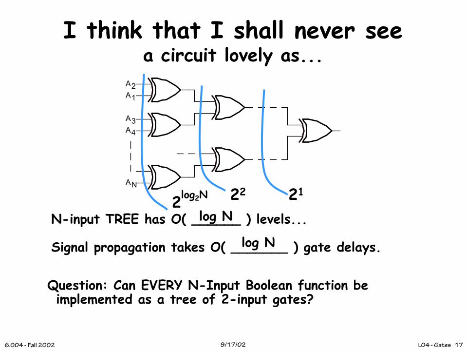
I think that I shall never seea circuit lovely as...
A1
A2
A4
A3
AN
N-input TREE has O( ______ ) levels...
Signal propagation takes O( _______ ) gate delays.
Question: Can EVERY N-Input Boolean function be implemented as a tree of 2-input gates?
log N
log N
21222log2N

L04 - Gates 186.004 - Fall 2002 9/17/02
Are Trees Always Best?Alternate Plan: Large Fan-in gates
N pulldowns with complementary pullups
Output HIGH if any input is HIGH = “OR”
Propagation delay: O( ____ )
since each additional MOSFET adds
...
N
N
tpd
O(log N)
O(N)
~4
Don’t be mislead by the “big O” stuff…
the constants in this case can be much
smaller… so for small N this plan might
be the best.
C

L04 - Gates 196.004 - Fall 2002 9/17/02
Here’s a Design Approach1) Write out our functional spec as a
truth table
2) Write down a Boolean expression for every ‘1’ in the output
3) Wire up the gates, call it a day, and declare success!
This approach will always give us Boolean expressions in a particular form: SUM-OF-PRODUCTS
C B A Y0 0 0 00 0 1 10 1 0 00 1 1 11 0 0 01 0 1 01 1 0 11 1 1 1
Truth Table
CBAACBBACABCY +++=

L04 - Gates 206.004 - Fall 2002 9/17/02
Straightforward SynthesisWe can implement
SUM-OF-PRODUCTS
with just three levels of
logic.
INVERTERS/AND/OR
Propagation delay --
No more than 3 gate delays
(ignoring fan-in)
ABC
ABC
ABC
ABC
Y

L04 - Gates 216.004 - Fall 2002 9/17/02
Oh, by the way…That Gate has a Name!
The gate we’ve been designing for this lecture is a
relatively important one: C B A Y0 0 0 00 0 1 10 1 0 00 1 1 11 0 0 01 0 1 01 1 0 11 1 1 1
Truth Table
A
BY
C
If C is 1 thencopy B to Y,
otherwise copyA to Y
2-input Multiplexer
A
B
C
0
1Gate
symbol(one) implementation
BCA
Y

L04 - Gates 226.004 - Fall 2002 9/17/02
Logic SimplificationCan we implement the same function with fewer gates?
Before trying we’ll add a few more tricks in our bag.
BOOLEAN ALGEBRA:
OR rules: a + 1 = 1, a + 0 = a, a + a = a
AND rules: a1 = a, aO = 0, aa = a
Commutative: a + b = b + a, ab = ba
Associative: (a + b) + c = a + (b + c),
(ab)c = a(bc)
Distributive: a(b+c) = ab + ac, a + bc =
(a+b)(a+c)
Complements:
Absorption:
Reduction:
DeMorgan’s Law:
0=,1=+ aaaa
babaaaaba +=+,=+
abbaaabaa =)+(,=)+(bbababbaab =)+)(+(,=+
babaabba +=,=+

L04 - Gates 236.004 - Fall 2002 9/17/02
Boolean Minimization:An Algebraic Approach
BACCBAACBABCY +++=
Lets (again!) simplify
Using the identity
ααα =+ AA
BACCBAACBABCY +++=
CBACY +=
BACCBABCY ++=
For any expression α and variable A:

L04 - Gates 246.004 - Fall 2002 9/17/02
Summary• Timing specs
• tPD: upper bound on time from valid inputs to valid outputs
• tCD: lower bound on time from invalid inputs to invalid outputs
• If not specified, assume tCD = 0
• Combinational logic
• Any function that can be specified by a truth table or, equivalently, in
terms of AND/OR/NOT (Boolean expression)
• Lenience: optional, more demanding functional guarantee. Rarely
needed; assume non-lenient logic by default.
• Minimally, we can get away with just 2-input NANDs or NORs
• Sum-of-products canonical form
• Comes directly from truth table
• “3-level” implementation of any logic function
• Limitations on number of inputs (fan-in) increases depth
• Next time: logic simplification, other canonical forms