Gas Sensor with Nanostructured Oxide Semiconductor Materials
19
Delivered by Ingenta to: Institute of Molecular and Cell Biology IP : 137.132.3.9 Tue, 19 Jun 2012 00:37:45 Copyright © 2011 American Scientific Publishers All rights reserved Printed in the United States of America Science of Advanced Materials Vol. 3, 150–168, 2011 Gas Sensor with Nanostructured Oxide Semiconductor Materials Ghim Wei Ho Department of Electrical and Computer Engineering, National University of Singapore, 4 Engineering Drive 3, Singapore 117576 Metal oxides are often the choice for conductometric gas sensing due to their thermal and envi- ronmental stability as well as good response reversibility. Due to the fact that sensing with these materials relies on interactions with the surface, one strategy to enhance the sensitivity is to increase the surface area or active sites by decreasing their physical dimensions. Nanoscale metal oxides such as nanoparticles, nanospheres, nanotubes, nanobelts and nanowires are routinely synthe- sized for development of solid-state gas sensors with improved sensing properties. In this review, gas sensing applications of a variety of metal oxide nanostructures in various device configurations; bulk, two-terminal and field effect transistor (FET) sensors are presented. The application of nano- structures as building blocks for sensor can be achieved by implementing effective assembly and integration techniques to transfer the nanostructures from growth substrates onto their respective device substrates. Two common methods have been reviewed which include transfer printing and dielectrophoretic alignment of nanowires. In essence, these approaches employ external forces to align the nanostructures via dry and wet media respectively. Finally, the non conventional substrates sensors such as textile and free standing nanowire sheet are reviewed. The non conventional sub- strates have the advantages of being flexible, shock proof, wearable and portable etc. Keywords: Metal Oxides, Sensors, Nanowires, Alignment, Field Effect Transistor. CONTENTS 1. Introduction ........................................ 150 2. Nanostructure Sensors ................................ 152 2.1. Bulk Nanostructure Sensor ......................... 152 2.2. Two-Terminal Thin Film Nanostructure Sensor ......... 154 2.3. FET Nanostructure Sensor ......................... 157 3. Directed Assembly of Nanostructure Sensors .............. 160 3.1. Transfer Printed Nanostructure Sensor ................ 160 3.2. Dielectrophoretic Assembled Nanostructure Sensor ............................. 161 4. Non-Conventional Substrate Sensor ...................... 163 4.1. Textile Sensor .................................. 165 4.2. Free Standing Sheet Sensor ........................ 166 5. Conclusions ........................................ 166 6. Future Directions .................................... 166 Acknowledgments ................................... 167 References and Notes ................................ 167 1. INTRODUCTION There is a great demand to enhance the sensitivity of chemical sensors for various sensing applications such as monitoring and conditioning of air quality, detection of flammable or toxic gases, medical diagnosis, detection of chemical-warfare agents, and optimization of combustion efficiency in automobile engines. Thus, the quality of gas sensors has a great impact in many areas such as environ- mental, domestic, public, automotive safety and security. There are three broad types of gaseous species that are often monitored and detected: —Toxic gas species (CO, SO 2 , NO x etc.) —Corrosive species (Cl 2 ,F 2 , HF etc.) —Explosive species (CH 4 , hydrocarbons, nitrous com- pounds etc.). Toxic gases are essentially being monitored in cities and homes, the corrosive gasses are monitored in chemical petrochemical and food industries and finally the explosive species are associated to public security. A typical sensor consists of three main parts: (i) sens- ing material where the molecular recognization or chemi- cal reactions take place, (ii) transducer which serves as an interface between the sensor and environment and trans- forms the molecular adsorption and/or chemical reactions into some physical parameters and (iii) signal processor system to quantify the physical parameter and feed the information back into a readable output. Sensors can be classified into various transducing principles. 1 The types of transducers include (i) electrical 150 Sci. Adv. Mater. 2011, Vol. 3, No. 2 1947-2935/2011/3/150/019 doi:10.1166/sam.2011.1145
Transcript of Gas Sensor with Nanostructured Oxide Semiconductor Materials

Delivered by Ingenta toInstitute of Molecular and Cell Biology
IP 13713239Tue 19 Jun 2012 003745
REVIEW
Copyright copy 2011 American Scientific PublishersAll rights reservedPrinted in the United States of America
Science ofAdvanced Materials
Vol 3 150ndash168 2011
Gas Sensor with Nanostructured OxideSemiconductor Materials
Ghim Wei HoDepartment of Electrical and Computer Engineering National University of Singapore
4 Engineering Drive 3 Singapore 117576
Metal oxides are often the choice for conductometric gas sensing due to their thermal and envi-ronmental stability as well as good response reversibility Due to the fact that sensing with thesematerials relies on interactions with the surface one strategy to enhance the sensitivity is to increasethe surface area or active sites by decreasing their physical dimensions Nanoscale metal oxidessuch as nanoparticles nanospheres nanotubes nanobelts and nanowires are routinely synthe-sized for development of solid-state gas sensors with improved sensing properties In this reviewgas sensing applications of a variety of metal oxide nanostructures in various device configurationsbulk two-terminal and field effect transistor (FET) sensors are presented The application of nano-structures as building blocks for sensor can be achieved by implementing effective assembly andintegration techniques to transfer the nanostructures from growth substrates onto their respectivedevice substrates Two common methods have been reviewed which include transfer printing anddielectrophoretic alignment of nanowires In essence these approaches employ external forces toalign the nanostructures via dry and wet media respectively Finally the non conventional substratessensors such as textile and free standing nanowire sheet are reviewed The non conventional sub-strates have the advantages of being flexible shock proof wearable and portable etc
Keywords Metal Oxides Sensors Nanowires Alignment Field Effect Transistor
CONTENTS
1 Introduction 1502 Nanostructure Sensors 152
21 Bulk Nanostructure Sensor 15222 Two-Terminal Thin Film Nanostructure Sensor 15423 FET Nanostructure Sensor 157
3 Directed Assembly of Nanostructure Sensors 16031 Transfer Printed Nanostructure Sensor 16032 Dielectrophoretic Assembled
Nanostructure Sensor 1614 Non-Conventional Substrate Sensor 163
41 Textile Sensor 16542 Free Standing Sheet Sensor 166
5 Conclusions 1666 Future Directions 166
Acknowledgments 167References and Notes 167
1 INTRODUCTION
There is a great demand to enhance the sensitivity ofchemical sensors for various sensing applications such asmonitoring and conditioning of air quality detection offlammable or toxic gases medical diagnosis detection ofchemical-warfare agents and optimization of combustion
efficiency in automobile engines Thus the quality of gassensors has a great impact in many areas such as environ-mental domestic public automotive safety and securityThere are three broad types of gaseous species that areoften monitored and detectedmdashToxic gas species (CO SO2 NOx etc)mdashCorrosive species (Cl2 F2 HF etc)mdashExplosive species (CH4 hydrocarbons nitrous com-
pounds etc)
Toxic gases are essentially being monitored in citiesand homes the corrosive gasses are monitored in chemicalpetrochemical and food industries and finally the explosivespecies are associated to public securityA typical sensor consists of three main parts (i) sens-
ing material where the molecular recognization or chemi-cal reactions take place (ii) transducer which serves as aninterface between the sensor and environment and trans-forms the molecular adsorption andor chemical reactionsinto some physical parameters and (iii) signal processorsystem to quantify the physical parameter and feed theinformation back into a readable outputSensors can be classified into various transducing
principles1 The types of transducers include (i) electrical
150 Sci Adv Mater 2011 Vol 3 No 2 1947-293520113150019 doi101166sam20111145
Delivered by Ingenta toInstitute of Molecular and Cell Biology
IP 13713239Tue 19 Jun 2012 003745
REVIEW
Ho Gas Sensor with Nanostructured Oxide Semiconductor Materials
(or electrochemical) transducers which transformchemical reactions into electrical signalsmdasheither cur-rent (amperometric sensors) or voltage (potentiometric)(ii) gravimetric transducers which register changes in massdue to molecular adsorption and (iii) optical transduc-ers which are based on different interferometry measurechanges in refractive index and thickness of membranescaused by different chemical reactions To realize a supe-rior solid-state gas sensor three well-known ldquoSrdquo whichis the sensitivity selectivity and stability of a sensor areoften studied and improvedThe sensitivity (S) of a sensor is defined as
S = dy
dx
the ability to detect a given analyte concentration whichis usually determined from a slope of an output signaly (eg a change in the electrical resistance) for a givenconcentration x of a specific gas to be detected23
The selectivity (Q of a sensor
Q= 100times dydxprime
dydx
is the ability to discriminate between a mixture of gaseswhich is defined by the cross sensitivity to all othergases23
Oxide materials represent an important class of materi-als whose properties cover the entire range from insulatorssemiconductors to metal In addition oxide materials pos-sess a broad range of electronic chemical and physicalproperties that are often highly sensitive to the changesin a chemical environment through a variety of detec-tion and transduction principles based on the semicon-ducting ionic conducting photoconducting piezoelectricpyroelectric and luminescence properties4ndash8
Thus the interest for gas-sensing applications of oxidematerials is continuously growing and further develop-ment of this field will require a constant effort towardsthe synthesis and processing of nanomaterials suitable forspecified applications Theoretically there is no limita-tion for the use of any oxide materials for gas sensing
Ghim Wei Ho is an assistant professor of Electrical and Computer Engineering in NationalUniversity of Singapore She received her PhD degree in Engineering from NanoscienceCentre University of Cambridge in 2006 MSc and BSc from National University ofSingapore in 2001 She is first in the world to develop novel SiC nanoflowers and multi-coaxial nanowires with media TV coverage in NBC ScienCentral and BBC News UK andmany newspaper coverages in Daily Telegraphy Cambridge Evening Newspaper StreatsHer Nanosicence and Nanosystems group is focused on fundamental science of the phys-ical and chemical processes of nanostructured materials synthesis unique properties andnanosystems The research focus involved the study of unique phenomena and manipulationof material at the nanoscale which revolves around the realization of solar cell chemicalsensor and drug delivery systems
applications However not all oxide materials are effec-tive sensors The selection of optimal sensing material ishighly dependent on the design manufacturing chemi-cal activity stability etc Because of the wide availabilityof synthesis and processing of oxides materials a carefulselection of methodology to prepare oxide of sufficientlyfine dispersion porous structure high crystallinity andbulk quantity is preferred Nevertheless novel synthesisand fabrication techniques as well as new material scienceand physics await discovery and remain to be exploredbased on the newly acquired nanoscience and nanotechnol-ogy knowledge At present various nanocrystalline oxidenanomaterial such as indium oxide (In2O3 titanium diox-ide (TiO2 gallium oxide (Ga2O3 zinc oxide (ZnO) tinoxide (SnO2 tungsten oxide (WO3 etc are synthesizedfor gas sensing applications9ndash14 Some information andoperating parameters about the commonly employed solid-state oxide gas sensing materials characteristics are sum-marized in the Table INanocrystalline oxide materials are classified into dif-
ferent categories depending on their dimensions and struc-tures Numerous oxide nanostructures of zero one andtwo-dimensional oxide nanostructures with suitable prop-erties composition and morphologies are routinely beingsynthesized for gas sensing applications The syntheticconditions to obtain nanocrystalline oxides product areextremely broad ranging from high temperatures andorpressures coupled with long processing times to very mildconditions without any applied pressure and even at roomtemperature Such a large variation of synthetic condi-tions is a result of the large variety of reactions avail-able in the formation of crystalline structures Generallythere are two methods of preparing oxide nanostructuresnamely the physical (dry) and chemical (wet) techniquesThe physical techniques include chemical vapor deposi-tion thermal vapor deposition solid-state reaction sput-tering etc starting from oxide powder oxide target inertgas to various reactive gasses The main structures thatare synthesized via physical methods are thin filmsnanowires nanotubes etc On the other hand chemicaltechniques include solndashgel hydrosolvothermal electrode-position Langmuir-Blodgett etc starting from various
Sci Adv Mater 3 150ndash168 2011 151
Delivered by Ingenta toInstitute of Molecular and Cell Biology
IP 13713239Tue 19 Jun 2012 003745
REVIEW
Gas Sensor with Nanostructured Oxide Semiconductor Materials Ho
Table I Properties and operating parameters on some of the commonly employed solid-state oxide gas sensing materials
Metal oxide Melting point Type of conductivity Operating temperature Optimal gas detection Stability Humidity sensitivity
SnO2 1900ndash1930 n 200ndash400 CO H2 CH4 Excellent HighGa2O3 1740ndash1805 n 400ndash1000 O2 CO NO2 NH3 Good LowIn2O3 1910ndash2000 n 200ndash400 O3 NO2 NH3 Fair LowTiO2 1855 n 350ndash800 O2 CO SO2 Fair LowZnO 1800ndash1975 n 250ndash350 CH4 C4H10 O2 NO2 NH3 Fair HighWO3 1470 n 200ndash500 O3 N2O SO2 H2S Excellent Low
oxide precursors solvents surfactants and additives Thestructures prepared by physical techniques have the advan-tages of being able to directly grow onto the final sub-strate and can be directly manipulated for the fabricatingof a nanodevice On the other hand the advantages ofproducing nanostructured materials using chemical routeis that large quantity of processable nanostructures can beobtained in a cost-effective highly-scalable and mild reac-tion condition
2 NANOSTRUCTURE SENSORS
Various oxide nanostructured materials are prepared anddeposited as thick thin film or incorporated into transis-tor for gas sensing applications15ndash20 The sensor perfor-mance depends on percolation path of electrons throughintergranular regions thus by varying small details inthe preparation process each sensor differs slightly inits sensing characteristics The first generation sensorsare prepared by thick film technology starting from pow-der Then comes along the thin film technology wherebyphysical deposition techniques are largely implementedThin films are developed based on vapor phase depositionusing chemical vapor deposition sputtering evaporationetc However the sensing performances are still not sat-isfactory due to a relatively low surface area of the pre-pared thick and thin films Another downside aspect ofboth the thin and thick films is the significant electricalproperties drift due to grain coalescence porosity modi-fication and grain-boundary issues These effects becomeespecially critical when the metal oxide active layers areoperated at relatively high temperature in order to guar-antee the reversibility of chemical reactions at the sur-face Thus several solutions have been put forward firstto increase the surface area by synthesizing nanostructuresand then to stabilize the nanostructure by eg addition ofa foreign element or phase Up to date various types ofdopants21 such as group-III (Al2223 Ga2425 In25) group-IV (Sn2526) group-V (N2223 P27 As2829 Sb30) group-VI(S31) and transition metal (Co32 Fe33 Ni34 Mn35) havebeen implanted into ZnO nanostructures Doping group-III and IV elements into ZnO has proven to enhance itsn-type conductivityMore recently a great step forward in the preparation
of a highly stable and sensitive sensor has been made
by incorporating single crystal one-dimensional semicon-ducting oxides nanostructures (nanobelts nanowires ornanoribbons) into the sensor36ndash45 The high crystallinityand the nanosized lateral dimension assure improved sta-bility and good sensing properties Their novel phenomenaand size effects make them interesting both for fundamen-tal studies and for potential nanodevice applications lead-ing to a third generation of oxide gas sensors
21 Bulk Nanostructure Sensor
The bulk nanostructure sensors that have been reportedconsist of nanostructures pressed into pellets46ndash48 coateddirectly as thick film on ceramic tube or nanostructuresgrown on substrate and directly fabricated as sensors49ndash54
Tan et al have reported SnO2 nanostructures pellet sensorwhere powders were processed into bulk sensor in a formof thick pellet (sim1 mm)48 Individual pellets were createdby adding 05 g of the SnO2 with embedded Pt wires andapplying a pressure of 15 tons on a mould The SnO2
nanoparticles were prepared by solid-state reaction syn-thetic route whereby reactions are usually initiated by self-initiation via grinding The solid-state reaction has severalunique features the reaction can be self-initiated at roomtemperature and internally produced heat can be self-sustained to produce crystalline products (Figs 1(andashd))The effects of various reaction parameters are investigatedto control the dimension of the SnO2 nanoparticles whichin turn were used for hydrogen sensing studies Figure 1(e)shows that the SnO2 nanostructure sensor exhibits highlyconsistent responses over many cycles which translatesto high device stability Figure 1(f) shows the sensitivityndashtemperature relationships obtained for different averageparticle sizes of 20 30 and 40 nm It is observed that sen-sors made up of smaller nanoparticles possess higher gassensitivities due to the increase in effective surface areaAnother type of bulk nanostructure sensors are based
on thick film coating on ceramic tube incorporated withheater55ndash57 Typically a ceramic tube is printed with metalelectrodes and conducting wires (Fig 2(a)) The workingtemperature of the sensor can be controlled by adjustingthe heating voltage across a resistor inside the ceramictube A reference resistor is put in series with the sensor toform a complete measurement circuit A working voltagewas applied and by monitoring the output voltage acrossthe reference resistor the response of the sensor in air or in
152 Sci Adv Mater 3 150ndash168 2011
Delivered by Ingenta toInstitute of Molecular and Cell Biology
IP 13713239Tue 19 Jun 2012 003745
REVIEW
Ho Gas Sensor with Nanostructured Oxide Semiconductor Materials
20 nm30 nm40 nm
(a)
(c) (d)
(b)(e)
(f)
Fig 1 SEM images of the SnO2 nanostructures obtained with variation in (andashb) precursor and (cndashd) additive concentrations (e) Typical currentresponse and (f) Sensitivityndashtemperature relationship of the bulk SnO2 nanostructure hydrogen sensor Reprinted with permission from 48 E T HTan et al Nanotechnology 19 255706 (2008) copy 2008 IOP Publishing
an analyte gas can be measured Guo et al have reportedFe2O3 porous nanorods and branched nanostructures bulksensors The nanostructures were synthesized by dehydra-tion and recrystallisation of -FeOOH precursor whichwas obtained from the hydrothermal reaction of FeCl3with urea in an aqueous system The morphology of theas-prepared nanostructures was characterized by TEM asshown in Figure 2(b) The inset shows the electron diffrac-tion pattern and ring which indicate the polycrystallinenature Figure 2(c) shows voltage response of the sensor ata working temperature of 150 C and 30 relative humid-ity It can be seen that output voltage values increasedabruptly on the injection of ethanol and then decreasedrapidly and recovered to their initial value after the testgas was released The response and recovery time of thenanostructure-based sensors were 1ndash3 and 4ndash8 s respec-tively There is also work reported on Fe2O3 nanotubeswhich show good ethanol sensing performance58
Similarly other bulk nanostructure sensor based on thickfilm coated on ceramic tube is also reported57 Homoge-neous In(OH)3 or InOOH colloidal supernatant was coatedonto a ceramic tube on which a pair of Au electrodes wasprinted After the solvent evaporation the colloidal crystalsform a thin film on the ceramic tube Then the ceramictube was annealed at 300 and 400 C for 2 h to transformIn(OH)3 or InOOH into cubic and hexagonal In2O3 respec-tively The conductance undergoes a drastic rise upon theinjection of reducing compound ethanol and drops to itsinitial value after ethanol is released These sensors showa quick response of less than 10 s and recovery time of15 s The lowest detection limit is down to 1 ppm The
response of the sensor correlates to the concentration ofthe test gas the structure and the morphology of In2O3
Another form of bulk nanostructure sensor is basedon nanowire grown and fabricated directly on the sub-strate From the viewpoint of device structure the conven-tional nanowire-based gas sensors were fabricated eitherby pick-and-place process of a single nanowire followedby making electrical contacts to individual nanowireThe device fabrication process uses expensive and timeconsuming procedures of sonication and dispersal ofnanowires on substrate with electrodes fabricated byelectron-beam lithography In this bulk nanowire sensordevice all these complicated processing steps can be elim-inated Figures 3(andashb) shows side and top-view SEMimages of ZnO nanowires grown on patterned electrodes59
Figure 3(c) shows the schematic diagram of the bulknanowire sensor device which was fabricated directly onthe growth substrate There are many nanowire-nanowirejunctions (Fig 3(d)) which act as electrical conductingpath Figure 3(e) shows the gas response as a functionof NO2 concentration at 225 C where the gas responseis directly proportional to gas concentration Figure 3(f)shows evidence of saturation at the NO2 concentrationlarger than 3 ppm This can be explained by the competi-tion between the adsorption sites versus the concentrationof target gas In a low gas concentration the availableadsorption sites on the surface of ZnO can be regardedas infinite compared with the NO2 concentration and thusthe rate-determining step might be the surface reactionbetween NO2 molecules and ZnO surface Thus surfacereactions are linearly dependent on the NO2 concentrationas long as adsorption sites are enough
Sci Adv Mater 3 150ndash168 2011 153
Delivered by Ingenta toInstitute of Molecular and Cell Biology
IP 13713239Tue 19 Jun 2012 003745
REVIEW
Gas Sensor with Nanostructured Oxide Semiconductor Materials Ho
(a)
(b)
(c)
Fig 2 (a) Schematic illustration of the gas sensor measurement system(b) TEM images of the as-synthesized Fe2O3 nanostructures (c) Real-time ethanol sensing characteristics of sensors based on the preparedFe2O3 nanostructures Reprinted with permission from [55] X L Gouet al Chem Eur J 14 5996 (2008) copy 2008 Wiley
Similarly bulk nanowire sensors were fabricateddirectly on nanowires grown on substrates60 Contactsto the multiple nanowires network were formed using ashadow mask and sputtering of AlTiAu electrodes Thesensor studies were on the time dependence of relative
resistance change of either metal-coated or uncoated net-work ZnO nanowire as the gas ambient is switched fromN2 to 500 ppm of H2 in air and then back to N2 Thehighest response is Pt coated nanowires which is followedby Pd while the other metals produce little or no changein response This is consistent with the known catalyticproperties of these metals for hydrogen dissociation Thesensors response to various gas concentrations and it candetect lt100 ppm H2 Other example of nanowire gas sen-sors which have been fabricated on Cd-Au comb-shapedinterdigitating electrodes is shown in Figures 3(gndashh)61 Thebulk nanowire sensors maintain high response to hydrogenconcentration in the range of 10 to 1000 ppm This highresponse is attributed to the highly connected network ofnanowires Similarly microtrench has been created on Sisubstrates and nanowires are grown using a thermal chem-ical vapor deposition and directly fabricated into sensor62
SnO2 nanowires are synthesized to be sufficiently long tobridge across trenched electrodes In this process compli-cated and individual alignment process is avoided and anumber of devices can be fabricated in a single processstep at a wafer scale The gas-sensing characteristics of thedeveloped sensor were significantly better when comparedto other types of NO2 sensors reported in the literatureThe sensitivity was gt150 at a NO2 concentration of 5 ppm
22 Two-Terminal Thin Film Nanostructure Sensor
Two terminal thin film sensor made up of one to fewmonolayer of nanostructures spanning across two elec-trodes are commonly fabricated The sensing device con-sists of a low-density layer of nanostructures whichare depositeddispersed onto preprepared coplanar elec-trodes Ho et al have reported on two-terminal meso-porous nanospheres thin film sensor (Fig 4(a))63 Thenanospheres (Figs 4(bndashc)) were synthesized based ona simple hydrothermal method using potassium stannatetrihydrate as a precursor in an ethanolndashdeionized watermixed solvent The parameters affecting the morphologyand porosity of the synthesized SnO2 nanostructures areinvestigated by varying various experimental conditionssuch as temperature precursor concentration and addi-tives The nanospheres grown without urea additive andat higher temperature (225 C) exhibit the highest spe-cific surface area of 1564 m2g with pore diameter of53 nm The nanospheres were diluted and dispersed inwater before drop casting a few monolayers onto the elec-trodes Figure 4(d) shows the current response graphsobtained by cycling it alternately in dry air and H2 at var-ious operating temperature It is noted that the responsetime (90 of RairndashRgas) is achieved within the first 13ndash30 min while the recovery time is 14ndash46 min depend-ing on the operating temperature of the sensor The effectof operating temperature of the reference sample on thesensor performance is investigated The responses of the
154 Sci Adv Mater 3 150ndash168 2011
Delivered by Ingenta toInstitute of Molecular and Cell Biology
IP 13713239Tue 19 Jun 2012 003745
REVIEW
Ho Gas Sensor with Nanostructured Oxide Semiconductor Materials
(c) (e)
(f)(b)
(a)
(d)
(g)
(h)
Fig 3 (a) Side and (b) top-view SEM images clearly show selective growth of ZnO nanowires on TiPt electrode (c) The schematic illustration ofZnO-nanowire air bridges over the SiO2Si substrate (d) The junction between ZnO nanowires grown on both electrodes (e) Responses of a nanowire-bridge ZnO gas sensor as a function of NO2 concentration (05ndash20 pm) at operating temperature of 225 C (f) Response versus NO2 concentrationplot which shows linear dependence in range of 05ndash3ppm (gndashh) Nanowire with interconnecting network for bulk nanowire sensing Figures 3(andashf)reprinted with permission from [59] M-W Ahn et al Sens Actuators B 138 168 (2009) copy 2009 Elsevier Limited Figures 3(gndashh) reprinted withpermission from [61] B Wang et al J Phys Chem C 112 6643 (2008) copy 2008 American Chemical Society
(a) (b) (c)
(d)
(f)
(e)
Fig 4 (a) Optical image of the fabricated sensor (bndashc) SEM images of SnO2 nanospheres synthesized at various reaction conditions (d) Responseand recovery times of the nanospheres sensor at various operating temperatures Response plot versus (e) operating temperature and (f) specific surfacearea of SnO2 nanospheres sensors Reprinted with permission from [63] S C Yeow et al Sens Actuators B 143 295 (2009) copy 2009 ElsevierLimited
Sci Adv Mater 3 150ndash168 2011 155
Delivered by Ingenta toInstitute of Molecular and Cell Biology
IP 13713239Tue 19 Jun 2012 003745
REVIEW
Gas Sensor with Nanostructured Oxide Semiconductor Materials Ho
sensor at different operating temperatures (200ndash450 C)are shown in Figure 4(e) As such a higher operatingtemperature leads to a greater change in conductance andhence greater response On the other hand desorption ofall oxygen ionic species previously adsorbed occurs at hightemperatures which explains the reduction in response asoperating temperature is increased beyond the optimumvalue Furthermore the effect of specific surface area onthe gas sensing performance is studied Figure 4(f) showsthe response plot obtained at 350 C for all the sampleswith different specific surface areas It can be observedthat it is not a linear relationship A possible explanationis that the inner surfaces of the porous nanospheres arenot fully utilized for gas detection due to the limitation ofdiffusion of the analyte gas through the nanoporesSysoev et al have reported thin film of nanoparticles
and nanowires sensor mounted on microchip64 The devicehas demonstrated an excellent performance as a gas sen-sor capable of detecting and discriminating between sev-eral reducing gases in air at a ppb level of concentra-tion Both nanoparticles film and nanowire mats weredeposited onto thermally oxidised SiO2Si substrates withPt strip electrodes and Pt meander heaters microarray TheSnO2 nanoparticles layers were deposited onto the sub-strates by spin-coating from an aqueous colloidal disper-sion of the nanoparticles (Fig 5(a)) SnO2 nanowires aredry transferred to substrate to yield one-two monolayernetwork of percolating nanowires (Fig 5(b)) Figures 5(cndashd) depict the experimental data on a long-term evolution of
(a)
(b)
(c)
(d)
Fig 5 HRTEM and SEM images of (a) SnO2 mesoporous nanoparticles layer and (b) SnO2 nanowires (c) Response and (d) resistance of thenanoparticles (open circles) and nanowires (filled circles) over time Reprinted with permission from [64] V V Sysoeva et al Sens Actuators B139 699 (2009) copy 2009 Elsevier Limited
the SnO2 nanostructures sensing characteristics toward the2-propanol vapor The response of nanowire mat to 1 ppmof 2-propanol is about sim64 The as-prepared nanoparti-cles sensor exhibits a high response of sim4times103 How-ever over 48 days the nanoparticle response drops rapidlyto 16 close to the nanowires sensor capability It hasbeen postulated that the initial high porosity nanoparti-cles allow high gas diffusion thus rendering high responseNevertheless the long-term exposure to 2-propanol vaporsat elevated operating temperature seems to facilitate sin-tering of nanoparticles Thus the two-terminal nanowiresensor is predicted to be a better conductometric gassensor with relatively high gas sensitivity and long-termstabilityOther work on two terminal sensors is based on SnO2
nanowires which were synthesized by thermal evaporationat 900 C65 The obtained nanowires were doped with pal-ladium by coating the nanowires with palladium chloride(PdCl2 and annealed at 350 C for 30 min in air in orderto decompose PdCl2 (Figs 6(andashb)) Gas sensors based onundoped 08 wt Pd-doped and 2 wt Pd-doped SnO2
nanowires were fabricated These SnO2 nanowire gas sen-sors showed a reversible response to H2 gas at operatingtemperature of 150 C (Figs 6(cndashd)) The sensor responseincreased with Pd concentration The 2 wt Pd-dopedSnO2 nanowire sensor showed a response as high as 253for 1000 ppm H2 gas at 100
C (Fig 6(d)) Pd doping hasdemonstrated to improve the sensor response and lowerthe operating temperature
156 Sci Adv Mater 3 150ndash168 2011
Delivered by Ingenta toInstitute of Molecular and Cell Biology
IP 13713239Tue 19 Jun 2012 003745
REVIEW
Ho Gas Sensor with Nanostructured Oxide Semiconductor Materials
(c)
(d)
(a) (b)
Fig 6 (andashb) TEM image of a 2 wt Pd-doped SnO2 nanowire with adiameter of 80 nm Inset shows the diffraction pattern of PdO nanopar-ticle on the nanowire Changes in the resistance of (c) undoped and(d) 2 wt Pd-doped SnO2 nanowire gas sensors upon exposure to 100200 400 800 and 1000 ppm of H2 gas Reprinted with permissionfrom [65] Y B Shen et al Sens Actuators B 135 524 (2009) copy 2009Elsevier Limited
(e)
Fig 7 (andashb) SEM images and (cndashd) IndashV curves of the single and multiple ZnO nanowire FETs respectively (e) The typical response curves ofthe single and multiple ZnO nanowire for variations of hydrogen concentration ranging from 50 to 100 ppm at 200 C Reprinted with permissionfrom [67] R Khan et al Sens Actuators B 150 389 (2010) copy 2010 Elsevier Limited
23 FET Nanostructure Sensor
In the case of field effect transistor sensor active nanowiresensor element can act as a resistive element whose resis-tance can be changed by the field-effect or charge transferprocess66ndash69 The sensing properties can be monitored byvarying the gate potential For instance Huang et al66 havereported a highly sensitive single Ga2O3 nanowire sensorwhich operates at room temperature although it is well-known fact that the Ga2O3 films sensors usually operateat high temperature of 400 to 1000 C The room temper-ature sensitivity observed here is most likely due to thegood crystallinity and ultrahigh surface-to-volume ratiosof the one-dimensional nanostructures The gas-sensingmeasurements were performed for an individual Ga2O3
nanowire device with two AuTi electrodes and the source-drain biased voltage fixed at 10 V When the individualGa2O3 nanowire is exposed to a mixed flow of ammonia(1000 ppm) and air the current is increased dramaticallyin the first 100 seconds and enhanced to about 30 timesand stabilized at sim7800 nA The Ga2O3 nanowire deviceexhibits a sensitivity of about 38 and a response time ofsim58 s in the ambient of 1000 ppm air-diluted NH3Khan et al have reported single and multiple nanowire
FET sensors67 Figures 7(a and b) show typical SEMimages of the single and multiple ZnO nanowire FETdevices70 For comparison purposes the distance betweenthe electrodes and the diameter of the ZnO nanowires werekept the same for both devices Figures 7(c and d) exhib-ited the typical electrical characteristics for the n-type sin-gle and multiple ZnO nanowire FETs respectively Themultiple nanowire devices showed greatly enhanced con-ductance due to increased number of nanowire Figure 7(e)shows the gas sensing characteristics as a function of timefor the single and multiple ZnO nanowires with varioushydrogen concentrations in the range of 50ndash100 ppm at200 C The sensor response was higher for the multiple
Sci Adv Mater 3 150ndash168 2011 157
Delivered by Ingenta toInstitute of Molecular and Cell Biology
IP 13713239Tue 19 Jun 2012 003745
REVIEW
Gas Sensor with Nanostructured Oxide Semiconductor Materials Ho
(a)
(b)
(c)
(d)
Fig 8 IndashVg curves before and after exposure to (a) 100-ppm NO2 and (b) 1 NH3 The response time of (c) 20 2 and 05 ppm NO2 and (d) 002NH3 Reprinted with permission from [68] C Li et al Appl Phys Lett 82 1613 (2003) copy 2003 American Institute of Physics
(a)
(b)
(c)
(d)
Fig 9 Schematic of (a) single and (b) multiple nanowire transistor structure where TiAu are deposited on nanowire-decorated SiSiO2 substrateas drain and source electrodes (c) IndashVg and (d) GGo versus time for the single and multi nanowire sensor device recorded at different NO2
concentrations Reprinted with permission from [72] D H Zhang et al Nano Lett 4 1919 (2004) copy 2004 American Chemical Society
158 Sci Adv Mater 3 150ndash168 2011
Delivered by Ingenta toInstitute of Molecular and Cell Biology
IP 13713239Tue 19 Jun 2012 003745
REVIEW
Ho Gas Sensor with Nanostructured Oxide Semiconductor Materials
ZnO nanowires than the response for the single ZnOnanowire over the entire range of hydrogen concentra-tion The multiple nanowires FET are made up of nano-junctions which acted as a potential barrier for electronflow The potential barrier decreased as the nanowire wasexposed to the reducing gas resulting in an increase inthe current flow The potential barrier modulation of mul-tiple nanowires was more efficient than the modulation ofthe surface depletion of the single ZnO nanowire in gassensing Therefore the potential barrier modulation in thenanojunctions caused the enhanced sensor response for themultiple nanowiresLi et al68 demonstrated the use of a single one-
dimensional nanowire FET sensor for high performanceroom temperature sensing The sensor is made up ofIn2O3 nanowires of diameter 10 nm and length 5 mwhich were placed between the source and drain elec-trodes with a silicon substrate as a back gate (Fig 8 inset)The as-fabricated In2O3 nanowire sensor devices exhib-ited typical n-type transistor characteristics The individualIn2O3 nanowire transistors sensors exhibited superior per-formance as such the sensitivity is of 106 for NO2 and 105
for NH3 which are four or five orders of magnitude betterthan results obtained from the thin-film based sensors71
Response times are as short as 5 s for 100-ppm NO2 and10 s for 1 NH3 The lowest detectable gas concentrationsare 05 ppm for NO2 and 002 for NH3
Furthermore the sensing and selectivity between dif-ferent gases can be studied by monitoring the currentdependence on the gate bias and the threshold voltageshift rendering a significant advantage over thin-film-based devices Figure 8(a) shows two currentndashgate volt-age (IndashVg) curves measured before and after exposure to100 ppm NO2 in argon with a constant source drain volt-age (Vds of minus03 V Both measurements suggest that theIn2O3 nanowires are n-type semiconductor as the con-ductance increase with gate bias There is also a pro-nounced shift in the threshold voltage from minus48 V before
(c)
Fig 10 (a) TEM of nanowires and nanobelts (b) Schematic view of device used for the in situ conductometric measurements under gas exposure andmetal deposition (c) Response of a pristine (dashed line) and Pd-functionalized (solid line) nanostructure to sequential oxygen and hydrogen pulses at473 K (top pane) and 543 K (bottom) Reprinted with permission from [73] A Kolmakov et al Nano Nano Lett 5 667 (2005) copy 2005 AmericanChemical Society
the exposure to 20 V after the exposure Adsorption ofoxidizing gases reduces the number of free electrons inthe n-type semiconductor and thus reduces the conductiv-ity Figure 8(b) shows two IndashVg curves before and afterexposing to diluted NH3 in Ar with Vds =minus03 V A largethreshold voltage shift from 248 V to 216 V is observedwith a maximum sensitivity of 105 at Vg = minus30 V ForNO2 concentrations of 20 2 and 05 ppm the responsetimes are determined to be 20 s 5 min and 10ndash12 minrespectively (Fig 8(c)) Figure 8(d) shows a response timeof about 2 min for 002 NH3 which is the lowest testedconcentration The limitation is imposed by the availabilityof highly diluted NH3 in air or argonZhang et al72 have demonstrated FET NO2 sensor down
to ppb levels based on both single and multiple In2O3
nanowires operating at room temperature as shown inschematic diagram Figures 9(a and b) Figure 9(c) showsthe conductance versus gate bias (Vg curves recorded inthe six different NO2 concentrations after exposure for20 min for single nanowire FET The threshold gate volt-age shifted rightward monotonically with the increasingNO2air concentration implying the gradual suppressionof carrier concentration of nanowire that scales linearlywith the absolute value of gate threshold As for the multinanowire FET the typical number of nanowires bridg-ing adjacent metal electrodes is estimated to be 100ndash200Figure 9(d) shows the sensing cycles of the multiwire FETdevice corresponding to NO2air concentrations of 5 1020 50 100 and 200 ppb The multiwire sensor showeda lower detection limit of 5 ppb compared to the 20 ppblimit of single nanowire sensors The room temperaturedetection limit is one of the lowest level ever reportedFurthermore selective detection of NH3 O2 CO and H2
is possible with this nanowire FET sensorKolmakov et al has demonstrated an enhanced 1-D
SnO2 nanostructure-based sensor with and without Pdnanoparticles decorated nanobelts (Fig 10(a))73 Thedeposited Pd works as catalysts for oxygen dissociation
Sci Adv Mater 3 150ndash168 2011 159
Delivered by Ingenta toInstitute of Molecular and Cell Biology
IP 13713239Tue 19 Jun 2012 003745
REVIEW
Gas Sensor with Nanostructured Oxide Semiconductor Materials Ho
Figure 10(b) shows the schematic view of device used forthe in situ conductometric FET measurements under gasexposure and metal deposition The sensing performanceof a SnO2 nanowire toward sequential oxygen and hydro-gen pulses at two different temperatures before (dashedcurves) and after (solid curves) Pd deposition is shownin Figure 10(c) Functionalizing the nanowire surface withPd leads to an enhancement in IDS response for both gasesand shorter response time Functionalizing the nanowiresurface with Pd leads to an enhancement in IDS responsefor both gases and to an increased speed of response Pdmetal nanoparticles grown on reduced n-SnO2 nanowiresand nanobelts were found to form Schottky-barrier likejunctions which locally deplete the nanostructure of elec-trons The improvements of sensitivity can be explained bythe combined ldquospillover effectrdquo of atomic oxygen formedcatalytically on the Pd particles then migrating onto thetin oxide and the back spillover effect in which weaklybound molecular oxygen migrate to the Pd and are cat-alytically dissociated Raising the temperature raises thevalue of IDS and shortens the response time of the sensorto O2 and H2 This effect is most prominent for oxygenfor which the nanostructure only becomes activated above543 K
3 DIRECTED ASSEMBLY OFNANOSTRUCTURE SENSORS
The application of nanostructures as building blocks forsensor can be achieved by implementing effective assem-bly and integration techniques to transfer the nanostructuresfrom growth substrates onto their respective device sub-strates Several methods have been developed to assembleone-dimensional nanostructures which include microflu-idic channel Langmuir-Blodgett blown bubble film self-assembled monolayers transfer printing alignment etcIn essence these approaches employ external forces toalign the nanostructures via wet or dry media In someapproaches multilayer alignment is possible while oth-ers allow selective spatial alignment in large-scale Thedevelopment of nanostructures based sensor generallyinvolves two processes First the assembly of nano-structures into highly integrated arrays with controlledorientation and spatial position second integration of inter-connects between nanostructures and the micro or macro-scopic subsystems
31 Transfer Printed Nanostructure Sensor
Transfer printing is a dry alignment technique wherebynanostructures are printed in contact or close proximityto the substrate allowing the nanostructures to be alignedin the same direction and in a predetermined densityThe nanostructures are grown on a substrate ldquostampsrdquoand then stamped ldquoprintedrdquo onto the receiving substrate
The receiving substrate can have pre deposited electrodesupon which nanostructures can be aligned The transferprinting deposition strategy has demonstrated to lead towell-defined and reproducible three-dimensional integratedcircuits structures of controlled nanowiresrsquo density andalignment over large substrate areas7475
Layer-by-layer assembly of nanowires for three-dimensional multifunctional electronics has been reportedby Javey et al74 The dry alignment process involves(i) optimized growth of designed nanowires by nanoclus-ter directed synthesis and(ii) patterned transfer of nanowires directly from ananowire growth substrate to a second device substrate viacontact printing (Figs 11(andashb))
In detail a photolithographically patterned device sub-strate is first firmly attached to a bench top and thenanowire growth substrate is placed face down in con-tact with the patterned device substrate A gentle man-ual pressure is then applied from the top followed bysliding the growth substrate by 1ndash3 mm before thegrowth substrate is removed Devices and circuits arethen fabricated on the printed arrays of nanowires usingconventional top-down lithography and metallization pro-cesses To fabricate a three-dimensional FET the con-tact printing of nanowires and device fabrication stepsare repeated several times along with the deposition ofSiO2 insulating layer in order to obtain vertically stackedelectronic layers (Figs 11(cndashd)) Another work which isalso reported by the same group is ordered arrays ofsingle-crystalline nano- and microwires of GaAs and InPwith well-controlled lengths widths and shape have beenfabricated over large areas from high quality bulk wafersby the use of traditional photolithography and anisotropicchemical wet etching75 Printing using elastomeric stampscan transfer these wire arrays to plastic substrates withexcellent retention of order and crystallographic orienta-tion of the wires Figure 11(e) shows the various printingconfiguration single to triple layers of nanowires patternsElectrical measurements on simple test structures demon-strate the high degree of mechanical flexibility of theresulting wire arrays on plastics The combination of topdown wire fabrication and transfer printing represents aneffective route to ultrahigh performance macroelectronicsystemsThe nanowires are observed to be cleanly printed
only at lithographically predefined locations FET device(Figs 14(cndashd)) The printed nanowires are aligned uni-formly across mm or larger scale with relatively highdensities (sim4 nanowirem) The monolithic integration ofindividual and parallel arrays of multifunctional and multi-layer circuits consists of up to 10 addressable vertical lay-ers This alignment methodology is applicable for the widerange of nanowire materials substrates and device designsFurthermore the simplicity and the low processing tem-perature requirement of the method makes it ideal for
160 Sci Adv Mater 3 150ndash168 2011
Delivered by Ingenta toInstitute of Molecular and Cell Biology
IP 13713239Tue 19 Jun 2012 003745
REVIEW
Ho Gas Sensor with Nanostructured Oxide Semiconductor Materials
(e)
Fig 11 Overview of 3D nanowire circuit integration (a) Contact printing of nanowire from growth substrate to prepatterned substrate (b) 3Dnanowire circuit is fabricated by the iteration of the contact printing device fabrication and separation layer deposition steps (c) Optical microscopeimage of 3D nanowire FETs (d) Dark field image shows a parallel array of nanowires aligned between source (S) drain (D) and top gate (G)electrodes Reprinted with permission from [74] A Javey et al Nano Lett 7 773 (2007) copy 2007 American Chemical Society (e) Images of singleto multiple layers of GaAs wire array which are transfer printed using elastomeric stamps Reprinted with permission from [75] Y G Sun and J ARogers Nano Lett 4 1953 (2004) copy 2004 American Chemical Society
achieving high performance three-dimensional integratedcircuitry with different functionalities in distinct layersTo demonstrate the potential of nanowire printing for
large-area sensor integration printed Si-nanowire arrayswere configured as H2 sensors P -type SiNWs were printedon Si substrates and two-terminal devices with Ni sili-cide contacts were fabricated77 The conductance of theSi nanowire array shows a strong dependence on the H2
exposure even at relatively low concentrations (250 ppm)It is worth noting that the nanowire printing method mayprovide a viable route toward the realization of electronicnoses and smart sensors capable of distinguishing chem-ical species while determining their concentrations Suchsensors may be envisioned through a large-scale integra-tion of different sensor components interfaced with signal-processing functions To achieve this goal heterogeneousassembly of nanowire materials with orthogonal sensitivityto different analytes is needed which may be achievedthrough a multistep nanowire printing process
32 Dielectrophoretic AssembledNanostructure Sensor
Dielectrophoresis (DEP) technique utilizes the dielectro-phoretic force acting on the particles to induce spatial
movement when exposed to a non uniform electric field inthe suspension medium The force depends on a numberof parameters such as the arrangement of the electrodethe frequency of the electric field and the resulting elec-tric field distribution as well as the dielectric propertiesof the particles and the surrounding medium By changingthese factors this force will pull the particle towards thehigher electric field region (positive DEP effect) or push ittowards the lower field region (negative DEP effect) DEPis a manipulation technique based on Maxwellrsquos classicalelectromagnetic field theory to allow controlled movementof particles in a controlled electric field between the presetelectrode structures The DEP technique has demonstratedthe potential for the construction of the nanosensors ornanoelectronic devices using as the nanostructured mate-rial as the building blocksJiang et al78 have reported work on manipulation of ZnO
nanorods by applying AC signals of suitable frequency andvoltage to provide non uniform electrical field on differentpatterns of electrode (Figs 12(andashb)) Similarly Li et al79
have proposed DEP assembly of nanowires onto interdigi-tated microelectrodes (Fig 12(c)) and mounted on micro-hotplate sensor platform (Fig 12(d))Template-assisted electrodeposition method and a
two-step thermal oxidation are employed Through
Sci Adv Mater 3 150ndash168 2011 161
Delivered by Ingenta toInstitute of Molecular and Cell Biology
IP 13713239Tue 19 Jun 2012 003745
REVIEW
Gas Sensor with Nanostructured Oxide Semiconductor Materials Ho
(a)
(b) (d)
(c)
Fig 12 (andashb) Low and high resolution SEM images of aligned ZnO nanowire in the interdigitated electrode array The voltage and the frequency ofthe applied electric field are 10 V and 5 kHz Reprinted with permission from [78] K W Jiang et al Sens Actuators B 134 79 (2008) copy 2008Elsevier Limited (c) Well dispersed and fairly aligned indiumtin nanowires bridged across the electrode array (d) Overview of the integrated sensorchip on micro-hotplate Reprinted with permission from [79] X P Li et al Sens Actuators B 148 404 (2010) copy 2008 Elsevier Limited
DEP(Sine waves)
Thermal andoxidationtreatment
Gas sensingmeasurement
Prefabrication of electrodes
Nanowire dispersion
Fig 13 Schematic of nanowire sensor integration nanowire suspension drop casting on interdigitated microelectrodes DEP assembly of metalnanowires alignment of nanowires on microelectrodes two-step thermal oxidation of nanowires and final integrated sensor chip The response curve ofthe various volatile organic compounds versus temperature Reprinted with permission from [80] T Jinkawa et al J Mol Catal A 155 193 (2000)copy 2008 Elsevier Limited
162 Sci Adv Mater 3 150ndash168 2011
Delivered by Ingenta toInstitute of Molecular and Cell Biology
IP 13713239Tue 19 Jun 2012 003745
REVIEW
Ho Gas Sensor with Nanostructured Oxide Semiconductor Materials
electrodeposition synthesis method one-dimensionalindium oxide tin oxide and indiumndashtin oxide nanowireswere successfully fabricated The nanowires are uniformand easy to process and assemble with good control ofchemical compositions The process flow of fabricatingnanowire sensor via DEP alignment process is shown inFigure 1380 The nanowires solution is prepared and dropcasted onto prefabricated interdigitated electrodes Thenanowires are observed to be randomly dispersed on theelectrodes The electrical field was generated by connect-ing a function generator to the interdigitated electrodeswhile a sinusoidal wave with a frequency of 5ndash6 MHzand peak-to-peak voltage of 6 V was applied during theDEP process At room temperature ethanol volatizedwithin minutes leaving nanowires aligned between theelectrode pairs Two thermal treatment processes werecarried out after the DEP assembly of nanowires to lowerthe contact resistance between the aligned nanowires andmicroelectrodes and increased the stability of the nanowireassembled First aligned metal nanowires were heated toabout 10 C below their melting points the temperaturevaried according to different material compositions Thebonding process was carried out in an inert nitrogenenvironment to prevent oxidation Next nanowires wereheated at the temperature just below the melting point ofthe respective material in an atmospheric environment for2 h The temperature was later raised to 400ndash500 C foranother 3 h to achieve full oxidation After the thermaland oxidation treatment the nanowire sensor chip wasready for electrical measurement and chemical response
ndash500
ndash400
ndash300
ndash200
ndash100
00
100
18E+10
22E+10
26E+10
30E+10
34E+10
38E+10
42E+10
0 600 1200 1800 2400 3000 3600 4200 4800
2500ppmH2
2000ppmH2
1154ppmH2
1000ppmH2
CDA CDA CDACDA
ndash350
ndash300
ndash250
ndash200
ndash150
ndash100
ndash50
00
50
100
40E+09
45E+09
50E+09
55E+09
60E+09
65E+09
70E+09
0 300 600 900 1200 1500 1800 2100 2400 2700
Time (s)
Time (s)
Res
ista
nce
(Ω)
Res
ista
nce
(Ω)
Sen
sitiv
ity (
)
Sen
sitiv
ity (
)
UV onUV on
UV off UV off
(a)
(c) (d)
(b)(e)
(f)
Fig 14 SEM images of (a) cotton textile substrate in low magnification (b) bare cotton fibres (c) ZnO nanorods-coated cotton fibres and (d) highmagnification images of ZnO nanorods on a cotton fibre Scale bar in the inset represents 100 nm Electrical responses of ZnO nanorods-on-cloth deviceto (e) various concentrations of H2 gas and (f) UV irradiation Clean dry air (CDA) was used to flush the chamber before and after each hydrogeninjection Experiments were performed in room temperature Reprinted with permission from [89] Z H Lim et al Sens Actuators B 151 121 (2010)copy 2010 Elsevier Limited
testing The sensor was investigated with different volatileorganic compounds The sensitivity of three alcohols isthe highest for methanol follow by ethanol isopropanolThese findings coincide with the number of methyl groupsin their chemical structure Two competitive dissociativereactions were proposed80 to explain the alcohol moleculesadsorbed on the oxide surface simply described as OndashHand CndashO bond-breaking processes where the former onehas a greater contribution to the resistance drop Thesensitivity order may relate to the preference of eachchemical over these two competitive reactions
4 NON-CONVENTIONAL SUBSTRATESENSOR
Technological and industrial difficulties in further minia-turization of devices have called for innovative ways toincorporate gadgets into articles of everyday life Thereare many sensors which have been fabricated on non con-ventional substrates namely the plastic textile and papersubstrate sensor The ability to fabricate sensor deviceson plastic substrates is important owing to the demandsof handheld portable consumer electronics Plastic sub-strates possess many attractive properties including bio-compatibility flexibility light weight shock resistancesoftness and transparency However plastics has low melt-ing point and they tend to deform or melt at tempera-tures of sim200 C This limits the synthesis temperatureof nanostructures directly on the plastic substrate Vari-ous ways to transfer the nanowires from donor substrate
Sci Adv Mater 3 150ndash168 2011 163
Delivered by Ingenta toInstitute of Molecular and Cell Biology
IP 13713239Tue 19 Jun 2012 003745
REVIEW
Gas Sensor with Nanostructured Oxide Semiconductor Materials Ho
to plastic substrate such as nanoimprint contact transferLangmuir Blogett etc have been developed In additionlow temperature synthesis processes have also been devel-oped to overcome this limitation Mc Alpine et al havereported plastic nanowire sensors based on Si nanowireswhich exhibit parts-per-billion sensitivity to NO2 a haz-ardous pollutant81
Another type of non conventional substrate sensor istextile Clothing is not only a necessity it also encom-passes a complete industry ranging from the down-to-earthbasics to the upmarket and chic Smart clothingtextiles arebecoming very popular in the past decade Smart textileswhich have been developed include silicon flexible skins
(b)
(a)
(d)
(c)
Source-meter
0
2E+09
4E+09
6E+09
8E+09
1E+10
12E+10
14E+10
16E+10
18E+10
I-V 1 I-V 2 I-V 3 I-V 4 I-V 5 Average
Res
ista
nce
(Ω)
Before After
(e)
(f)
(g)
Fig 15 SEM images of (a) low resolution ZnO-nanorods-coated textile with selected area (circled in red) for subsequent studies (b) the selected ZnOnanorods-coated yarns before stretching twisting and sonication (c) the same yarns after repeated stretching and twisting and (d) 5 minutes of watersonification (e) Schematic diagram of the electro-mechanical testing and (f) electrical properties before and after each stretching and twisting cycle(g) Electrical measurement of ZnO nanorods-on-cloth device while subjected to controlled stress cycles with a mechanical testing system Reprintedwith permission from [89] Z H Lim et al Sens Actuators B 151 121 (2010) copy 2010 Elsevier Limited
and organic transistors on textile fibers8283 Another type ofthe smart sensing textiles which uses piezo-resistive prop-erties has been developed The approach for fabricating thefabrics was to coat a thin layer of piezo-resistive materialssuch as polypyrrole or a mixture of rubbers and carbonson conventional fabrics to form fabric-based sensors84ndash86
The function of the developed sensors is similar to that offlexible strain gauges which can measure strains when theyare subjected to a tensile stress Other innovations whichare not actively explored are textiles which can detectenvironmental conditions which then react and adapt toenvironmental changes Furthermore smart textiles can bemade to measure and monitor the physiological conditions
164 Sci Adv Mater 3 150ndash168 2011
Delivered by Ingenta toInstitute of Molecular and Cell Biology
IP 13713239Tue 19 Jun 2012 003745
REVIEW
Ho Gas Sensor with Nanostructured Oxide Semiconductor Materials
of the wearer eg perspiration heartbeat etc Thus they canbe applied various healthcare systems
41 Textile Sensor
While the development of wearable devices has beenreported the incorporation of nano-materials into thedesigns has not been well explored In addition problemssuch as complex process mass production washabilityand wearing comforts needs to be well addressed The easeof synthesizing ZnO nanowires or nanorods on almost anysubstrates welcomes large-scale incorporation on textileZnO nano-structures are believed to be non-toxic and bio-safe87 allowing their direct usage in daily applicationsWhile the use of nano-materials in daily human activitiesraised questions on its potential health risks there is todate no in vivo evidence of toxicity of nano-particulateZnO88
29 nm
5 nm
1 μm1 μm
2 nm 5 μm
15Endash03
16Endash03
17Endash03
18Endash03
Time (s)
on off
1000 ppm
(a)
(c) (d)(f)
(b) (e)
15Endash03
16Endash03
16Endash03
17Endash03
17Endash03
18Endash03
18Endash03
150 250 350 450 550 650 0 150 300 450 600 750 900
Time (s)
Cur
rent
(m
A)
Cur
rent
(m
A)
on off
2000 ppm1500 ppm
1000 ppm2500 ppm
(g) (h)
Fig 16 (andashb) Low and (cndashd) high resolution TEM images of the nanobelts (e) Image of nanobelts sheet made without any addition of binder orreinforcement chemicals (f) Cross-sectional SEM image of the nanobelts sheet Current response of the sensor at (g) varying and (h) same ppm H2
concentration Reprinted with permission from [90] S Bela et al J Phys D Appl Phys 43 35401 (2010) copy 2010 Institute of Physics
SEM images of the textile and nanorods displayed inFigures 14(andashd) show radially oriented nanorods (diametersim80 nm) with hexagonal cross-section grown along thecylindrical fibres (diameter sim15 m)89 Length of thenanorods is sim1 m The nanorods form a uniform anddense coverage around entire lengths of the fibres to forma cross-linked semi-conductive textileThe conductive textile shows excellent multiple sens-
ing (gas and optical) performances at room temperature asshown in Figures 14(e) and (f) respectively In the presenceof hydrogen gas chemisorbed oxygen ions are reducedto release electrons to the conduction band of the ZnOsurface resulting in an increase in conductivity In addi-tion the reduction reaction decreases the surface densityof the oxygen adsorbate leading to a reduction in thewidth of the depletion region and the height of the sur-face potential barrier thus resulting in the decrease in theresistance of the sensor The mechanism for UV sensing
Sci Adv Mater 3 150ndash168 2011 165
Delivered by Ingenta toInstitute of Molecular and Cell Biology
IP 13713239Tue 19 Jun 2012 003745
REVIEW
Gas Sensor with Nanostructured Oxide Semiconductor Materials Ho
is similar to that of hydrogen sensing with holes fromthe photo-generated electronndashhole pairs playing the role ofremoving the adsorbed oxygen molecules insteadA notable feature of the ZnO nanorods-coated textile
device is its fine morphological and electrical stabilityunder multiple stress and washing cycles A critical chal-lenge of semi-conductive yarns and textile is its durabil-ity and constancy of electrical performance SEM analyses(Figs 15(andashd)) of the nanorods -on-cloth before and afterstretching twisting and ashing cycles show no cracks ordelamination of the nanorods from the fibres respectivelyFigure 15(e) shows a schematic of the electro-mechanicaltesting Electrical characterisations made before and aftereach stretching and twisting cycle (Fig 15(f)) show goodelectrical stability We further perform electrical conduc-tivity measurements while stretching and relaxing the tex-tile device in a controlled manner The semiconductingtextile exhibits a higher conductivity when stretched dueto tighter packing (increased contact junctions) of the ZnOnanorods-coated fibers Figure 15(g) shows the variation ofcurrent through the textile device as it underwent repeatedcycles of stress and relaxation When the stress is releasedconductivity falls and stabilises to the original state Againthe morphology of the nanorods-on-textile suffered nocracks of delamination or noticeable degradation after theelectromechanical testing
42 Free Standing Sheet Sensor
Another non conventional sensor substrate is a free stand-ing sheet of nanowire paper The nanostructures are tobe produced in gram quantities so that it can be easilymade into nanostructured paper sheet The thickness ofthe nanostructures sheet can be tuned according to theamount of nanostructures used After the filtering wascompleted a sheet of nanostructures was formed by sand-wiching between a metal calender which was pressed andheated to ensure the nanowires are well dried and bondedtogether to form the free-standing paperBela et al have been reported synthesis of hybrid
titanate and titania nanobelts (Figs 16(andashd)) in a large-scale quantity for gas sensing applications90 The nanobeltsare synthesized from TiO2 powder based on hydrolysis andion exchange of NaOH base and HCl acid respectivelySheets of as-synthesized nanobelts are used for electricaland gas sensing measurements Figure 16(e) shows thewhite nanobelts sheet made without any addition of binderor reinforcement chemicals Cross-sectional SEM image ofFigure 16(f) shows that the nanobelts sheet has a thicknessof sim15 m Figures 16(g and h) show the current responseof the sensor at varying and same ppm H2 concentra-tions respectively The measurements were conducted at anoperating temperature of 300 C From the graphs it is evi-dent that the introduction of hydrogen causes the resistanceof the sensor to reduce because of the injection of electrons
onto the surface of the metal-oxide nanostructures therebyimproving the conductivity of the bulk sensing capabili-ties The resistance increases as the concentration of H2 isvaried from 2500 to 1000 ppm The response time (90of Rair minusRgas is achieved within the first 40ndash50 s whilethe recovery time is 10ndash12 min From the Figure 7(c) itwas observed that the sensing response was rather stableand reversible In oxidizing atmosphere of 300 C ambi-ent oxygen is adsorbed on the surface of nanobelts mostlikely with a negative charge Subsequently with the intro-duction of a reducing H2 gas it reacts with the negativelycharged surface oxygen and decreases the resistance bythe injection of electron
5 CONCLUSIONS
There is an immense technological and scientific potentialsof nanostructured materials in nanodevice applicationsand already numerous nanomaterial based sensors usingvarious materials have been reported These oxide materi-als can be synthesized by various synthetic routes whichinclude both physical and chemical methods The poten-tial application of these nanostructures as sensor dependsgreatly on the ability to precisely control their dimensionchemical composition surface property phase purity andcrystal structure Sensor of various configurations bulktwo-terminal and FET device have been fabricated Theintegrability of the nanostructure sensor into microelec-tronic fabrication technology is an issue that needs tobe addressed Various ways to assemble nanowires so asto ease the device fabrication process have been devel-oped The recent advances in assembling larger and morecomplex nanowire sensor arrays and integrating them intonanoscale electronics can lead to exquisite sensor sys-tem performances These sensory systems can sensitivelytransduce gaschemicalbiological binding events into elec-tronicdigital signals which promise a sophisticated nano-electronics sensing system
6 FUTURE DIRECTIONS
Although nanomaterial based sensors are expected to out-perform their bulk component there are still many issuesand parameters to be studied and addressed Parameters tobe explored include structural and composition tuning aswell as doping and functionalization of surfaces to increaseselectivity sensitivity and materials integrity for long-termstability Other parameters such as limits of detection lim-its of quantification dynamic range response and recov-ery times and lifetime have to be studied and improvedas well The long-term reliability of a sensor is impor-tant since progressive drifts in the characteristics andorresponses of the sensors affect accurate testing and analy-sis The drift of the sensors are frequently related to highworking temperatures and exposure to chemically active
166 Sci Adv Mater 3 150ndash168 2011
Delivered by Ingenta toInstitute of Molecular and Cell Biology
IP 13713239Tue 19 Jun 2012 003745
REVIEW
Ho Gas Sensor with Nanostructured Oxide Semiconductor Materials
ambient gas Many other issues include aging grain-sizegrowth poisoning due to unknown chemical species dif-fusion processes within the device etc are to be addressedas wellThe future direction of the solid-state gas sensor is
towards integrated wirelessremote multi-purpose sens-ing high selectivity recognition of a specific biological orchemical species with ldquoelectronic-nose-tonguerdquo capabili-ties In addition development of miniaturized analyticalsensor which can be integrated in-line orand as standaloneportable sensors is paramount for industrial applicationsThe sensors can further be refined into a network of sensorarrays providing rapid screening monitoring and reportingsystem The data are collected in a database and form partof a feedback guidance system to the control algorithm inindustrial processes
Acknowledgments The work is supported by NationalUniversity of Singapore grant R-263-000-532-112Images used for the cover page are kindly contributed byZ H Lee and M Kevin multidisciplinary laboratory
References and Notes
1 D James S M Scott Z Ali and W T OrsquoHare Microchim Acta149 1 (2005)
2 C-D Kohlin Nanoelectronics and Information Technology editedby R Waser Wiley-VCH Berlin (2005) p 851
3 M E Franke T J Koplin and U Simon Small 2 36 (2006)4 A Kolmakov and M Moskovits Annu Rev Mater Res 34 151
(2004)5 A Mandelis and C Christofides Physics Chemistry and Technology
of Solid State Gas Sensor Devices Wiley-Interscience New York(1993)
6 P T Moseley Sens Actuators B 6 149 (1992)7 N M White and J D Turner Meas Sci Technol 8 1 (1997)8 D Kohl J Phys D 34 R125 (2001)9 N Pinna G Neri M Antonietti and M Niederberger Angew
Chem Int Ed 43 4345 (2004)10 L P Sun L H Huo H Zhao S Gao and J G Zhao Sens Actu-
ators B 114 387 (2006)11 Z F Liu T Yamazaki Y B Shen T Kikuta N Nakatani and
Y X Li Sens Actuators B 129 666 (2008)12 C S Rout A R Raju A Govindaraj and C N R Rao J Nanosci
Nanotechnol 7 1923 (2007)13 M S Arnold P Avouris Z W Pan and Z L Wang J Phys
Chem B 107 659 (2003)14 I Jimenez I M A Centeno R Scotti F Morazzoni A Cornet
and J R Morante J electrochem Soc 150 H72 (2003)15 S Semancik and R E Cavicchi Thin Solid Films 206 81 (1991)16 N S Baik G Sakai N Miura and N Yamazoe Sens Actuators B
63 74 (2000)17 M Ivanovskaya P Bogdanov G Faglia and G Sberveglieri Sens
Actuators B 68 344 (2000)18 K Ihokura and I Watson The Stannic Oxide Gas Sensormdash
Principles and Applications CRC Press Boa Raton (1994)19 K D Schierbaum U Weimar and W Gopel Sens Actuators B
7 1 (1992)20 G Korotcenkov Sens Actuators B 121 664 (2007)21 J G Lu P C Chang and Z Y Fan Mater Sci Eng 52 49 (2006)22 T Yamamoto and H Katayama-Yoshida Jpn J Appl Phys
38 L166 (1999)
23 J G Lu L P Zhu Z Z Ye F Zhuge B H Zhao D W MaL Wang and J Y Huang J Mater Sci 41 467 (2006)
24 J Zhong S Muthukumar Y Chen Y Lu H M Ng W Jiang andE L Garfunkel Appl Phys Lett 83 3401 (2003)
25 S Y Bae C W Na J H Kang and J Park J Phys Chem B109 2526 (2005)
26 S Y Li P Lin C Y Lee T Y Tseng and C J Huang J Phys DAppl Phys 37 2274 (2004)
27 D K Hwang H S Kim J H Lim J Y Oh J H Yang S J ParkK K Kim D C Look and Y S Park Appl Phys Lett 86 151917(2005)
28 W Lee M C Jeong S W Joo and J M Myoung Nanotechnology16 764 (2005)
29 W Lee M C Jeong and J M Myoung Appl Phys Lett 85 6167(2004)
30 D W Zeng C S Xie B L Zhu R Jiang X Chen W L SongJ B Wang and J Shi J Cryst Growth 266 511 (2004)
31 G Z Shen J H Cho J K Yoo G C Yi and C J Lee J PhysChem B 109 5491 (2005)
32 J B Cui and U J Gibson Appl Phys Lett 87 133108 (2005)33 C X Xu X W Sun Z L Dong M B Yu Y Z Xiong and J S
Chen Appl Phys Lett 86 173110 (2005)34 D A Schwartz K R Kittilstved and D R Gamelin Appl Phys
Lett 85 1395 (2004)35 C Ronning P X Gao Y Ding Z L Wang and D Schwen Appl
Phys Lett 84 783 (2004)36 A J Mieszawska R Jalilian G U Sumanasekera and F P
Zamborini Small 3 722 (2007)37 B Zhu K Li S Zhang S Wu and W Huang Prog Chem 20 48
(2008)38 J X Wang S S Xie and W Zhou MRS Bull 32 123 (2007)39 W Lu and C M Lieber J Phys D-Appl Phys 39 R387
(2006)40 X Wang and Y D Li Inorganic Chemistry 45 7522 (2006)41 Y Shen T Yamazaki Z Liu D Meng T Kikuta N Nakatani
M Saito and M Mori Sens Actuators B 135 524 (2009)42 A Kolmakov Y Zhang G Cheng and M Moskovits Adv Mater
15 997 (2003)43 X T Zhou J Q Hu C P Li D D D Ma C S Lee and S T
Lee Chem Phys Lett 369 220 (2003)44 T-J Hsueh C-L Hsu S-J Chang and I-C Chen Sens Actua-
tors B 126 473 (2007)45 Q Wan Q H Li Y J Chen T H Wang X L He J P Li and
C L Lin Appl Phys Lett 84 3654 (2004)46 G J Li X H Zhang and S Kawi Sens Actuators B 60 64 (1999)47 G J Li and S Kawi Talanta 45 759 (1998)48 E T H Tan G W Ho A S W Wong S Kawi and A T S Wee
Nanotechnology 19 255706 (2008)49 S Luo G Fu H Chen and Y Zhang Mater Chem Phys 109 541
(2008)50 C Y Wang M Ali T Kups C C Roehlig V Cimalla T Stauden
and O Ambacher Sens Actuators B 130 589 (2008)51 J Ahmed S Vaidya T Ahmad P Sujatha Devi D Das and A K
Ashok Mater Res Bull 43 264 (2008)52 J Kaur R Kumar and M C Bhatnagar Sens Actuators B
126 478 (2007)53 D Lutic M Strand A Lloyd-Spetz K Buchholt E Ieva P O
Kall and M Sanati Top Cata 45 105 (2007)54 A Teleki S E Pratsinis K Kalyanasundaram and P I Gouma
Sens Actuators B 119 683 (2006)55 X L Gou G X Wang X Y Kong D Wexler J Horvat J Yang
and J Park Chem Eur J 14 5996 (2008)56 X Feng Z J Li P Y Wang and Y F Zhou J Mat Sci 40 6597
(2005)57 J Chen L Xu W Li and X Gou Adv Mater 17 582 (2005)58 Z B Zhuang Q Peng J F Liu X Wang and Y D Li Inorg
Chem 46 5179 (2007)
Sci Adv Mater 3 150ndash168 2011 167
Delivered by Ingenta toInstitute of Molecular and Cell Biology
IP 13713239Tue 19 Jun 2012 003745
REVIEW
Gas Sensor with Nanostructured Oxide Semiconductor Materials Ho
59 M-W Ahn K-S Park J-H Heo D-W Kim K J Choi and J-GPark Sens Actuators B 138 168 (2009)
60 H T Wang B S Kang F Ren L C Tien P W Sadik D PNorton S J Pearton and J Lin Appl Phys A 81 1117 (2005)
61 B Wang L F Zhu Y H Yang N S Xu and G W Yang J PhysChem C 112 6643 (2008)
62 T H Jung S-I Kwon J-H Park D-G Lim Y-J Choi and J-GPark Appl Phys A 91 707 (2008)
63 S C Yeow W L Ong A S W Wong and G W Ho Sens Actu-ators B 143 295 (2009)
64 V V Sysoeva T Schneiderb J Goschnickb I KiselevbW Habichtb H Hahnb E Strelcovc and A Kolmakov Sens Actu-ators B 139 699 (2009)
65 Y B Shen T Yamazaki Z F Liu D Meng T Kikuta N NakataniM Saito and M Mori Sens Actuators B 135 524 (2009)
66 Y Huang S Yue Z Wang Q Wang C Shi Z Xu X D BaiC Tang and C Gu J Phys Chem B 110 796 (2006)
67 R Khan H-W Ra J T Kim W S Jang D Sharma and Y HIm Sens Actuators B 150 389 (2010)
68 C Li D H Zhang X L Liu S Han T Tang J Han and C ZhouAppl Phys Lett 82 1613 (2003)
69 Z Fan and J G Lu Appl Phys Lett 86 123510 (2005)70 Z Y Fan D W Wang P C Chang W Y Tseng and J G Lu
Appl Phys Lett 85 5923 (2004)71 M Liess Thin Solid Films 410 183 (2002)72 D H Zhang Z Q Liu C Li T Tang X L Liu S Han B Lei
and C W Zhou Nano Lett 4 1919 (2004)73 A Kolmakov D O Klenov Y Lilach S Stemmer and
M Moskovits Nano Lett 5 667 (2005)74 A Javey S W Nam R S Friedman H Yan and C M Lieber
Nano Lett 7 773 (2007)75 Y G Sun and J A Rogers Nano Lett 4 1953 (2004)
76 Z Fan J C Ho Z A Jacobson R Yerushalmi R L AlleyH Razavi and A Javey Nano Lett 8 20 (2008)
77 Z Y Fan J C Ho T Takahashi R Yerushalmi K Takei A CFord Y-L Chueh and A Javey Adv Mater 21 3730 (2009)
78 K W Jiang W J Liu L J Wan and J Zhang Sens Actuators B134 79 (2008)
79 X P Li E China H W Sun P Kurup and Z Y Gu Sens Actu-ators B 148 404 (2010)
80 T Jinkawa G Sakai J Tamaki N Miura and N Yamazoe J MolCatal A 155 193 (2000)
81 M C McAlpine H Ahmad D W Wang and J R Heath NatMater 6 379 (2007)
82 R B Katragadda and Y Xu A Novel Intelligent Textile TechnologyBased on Silicon Flexible Skins Electrical and Computer Engineer-ing Wayne State University Detroit Michigan USA ISWC (2005)pp 78ndash81
83 J B Lee and V Subramanian IEEE Trans Electron Devices 62 269(2005)
84 R Wijesiriwardana K Mitcham and T Dias Fibre-meshed trans-ducers based real time wearable physiological information moni-toring system Proceedings of the 8th International Symposium onWearable Computers ISWCrsquo04 (2004) pp 40ndash47
85 R Wijesiriwardana IEEE Sens J 6 571 (2006)86 E P Scilingo F Lorussi A Mazzoldi and D De Rossi Sens J
IEEE 3 460 (2003)87 J Zhou N Xu and Z L Wang Adv Mater 18 2432 (2006)88 G J Nohynek E K Dudour and M S Roberts Nanotechnology
21 136 (2008)89 Z H Lim Z X Chia M Kevin A S W Wong and G W Ho
Sens Actuators B 151 121 (2010)90 S Bela A S W Wong and G W Ho J Phys D Appl Phys
43 35401 (2010)
Received 4 November 2010 Accepted 20 January 2011
168 Sci Adv Mater 3 150ndash168 2011

Delivered by Ingenta toInstitute of Molecular and Cell Biology
IP 13713239Tue 19 Jun 2012 003745
REVIEW
Ho Gas Sensor with Nanostructured Oxide Semiconductor Materials
(or electrochemical) transducers which transformchemical reactions into electrical signalsmdasheither cur-rent (amperometric sensors) or voltage (potentiometric)(ii) gravimetric transducers which register changes in massdue to molecular adsorption and (iii) optical transduc-ers which are based on different interferometry measurechanges in refractive index and thickness of membranescaused by different chemical reactions To realize a supe-rior solid-state gas sensor three well-known ldquoSrdquo whichis the sensitivity selectivity and stability of a sensor areoften studied and improvedThe sensitivity (S) of a sensor is defined as
S = dy
dx
the ability to detect a given analyte concentration whichis usually determined from a slope of an output signaly (eg a change in the electrical resistance) for a givenconcentration x of a specific gas to be detected23
The selectivity (Q of a sensor
Q= 100times dydxprime
dydx
is the ability to discriminate between a mixture of gaseswhich is defined by the cross sensitivity to all othergases23
Oxide materials represent an important class of materi-als whose properties cover the entire range from insulatorssemiconductors to metal In addition oxide materials pos-sess a broad range of electronic chemical and physicalproperties that are often highly sensitive to the changesin a chemical environment through a variety of detec-tion and transduction principles based on the semicon-ducting ionic conducting photoconducting piezoelectricpyroelectric and luminescence properties4ndash8
Thus the interest for gas-sensing applications of oxidematerials is continuously growing and further develop-ment of this field will require a constant effort towardsthe synthesis and processing of nanomaterials suitable forspecified applications Theoretically there is no limita-tion for the use of any oxide materials for gas sensing
Ghim Wei Ho is an assistant professor of Electrical and Computer Engineering in NationalUniversity of Singapore She received her PhD degree in Engineering from NanoscienceCentre University of Cambridge in 2006 MSc and BSc from National University ofSingapore in 2001 She is first in the world to develop novel SiC nanoflowers and multi-coaxial nanowires with media TV coverage in NBC ScienCentral and BBC News UK andmany newspaper coverages in Daily Telegraphy Cambridge Evening Newspaper StreatsHer Nanosicence and Nanosystems group is focused on fundamental science of the phys-ical and chemical processes of nanostructured materials synthesis unique properties andnanosystems The research focus involved the study of unique phenomena and manipulationof material at the nanoscale which revolves around the realization of solar cell chemicalsensor and drug delivery systems
applications However not all oxide materials are effec-tive sensors The selection of optimal sensing material ishighly dependent on the design manufacturing chemi-cal activity stability etc Because of the wide availabilityof synthesis and processing of oxides materials a carefulselection of methodology to prepare oxide of sufficientlyfine dispersion porous structure high crystallinity andbulk quantity is preferred Nevertheless novel synthesisand fabrication techniques as well as new material scienceand physics await discovery and remain to be exploredbased on the newly acquired nanoscience and nanotechnol-ogy knowledge At present various nanocrystalline oxidenanomaterial such as indium oxide (In2O3 titanium diox-ide (TiO2 gallium oxide (Ga2O3 zinc oxide (ZnO) tinoxide (SnO2 tungsten oxide (WO3 etc are synthesizedfor gas sensing applications9ndash14 Some information andoperating parameters about the commonly employed solid-state oxide gas sensing materials characteristics are sum-marized in the Table INanocrystalline oxide materials are classified into dif-
ferent categories depending on their dimensions and struc-tures Numerous oxide nanostructures of zero one andtwo-dimensional oxide nanostructures with suitable prop-erties composition and morphologies are routinely beingsynthesized for gas sensing applications The syntheticconditions to obtain nanocrystalline oxides product areextremely broad ranging from high temperatures andorpressures coupled with long processing times to very mildconditions without any applied pressure and even at roomtemperature Such a large variation of synthetic condi-tions is a result of the large variety of reactions avail-able in the formation of crystalline structures Generallythere are two methods of preparing oxide nanostructuresnamely the physical (dry) and chemical (wet) techniquesThe physical techniques include chemical vapor deposi-tion thermal vapor deposition solid-state reaction sput-tering etc starting from oxide powder oxide target inertgas to various reactive gasses The main structures thatare synthesized via physical methods are thin filmsnanowires nanotubes etc On the other hand chemicaltechniques include solndashgel hydrosolvothermal electrode-position Langmuir-Blodgett etc starting from various
Sci Adv Mater 3 150ndash168 2011 151
Delivered by Ingenta toInstitute of Molecular and Cell Biology
IP 13713239Tue 19 Jun 2012 003745
REVIEW
Gas Sensor with Nanostructured Oxide Semiconductor Materials Ho
Table I Properties and operating parameters on some of the commonly employed solid-state oxide gas sensing materials
Metal oxide Melting point Type of conductivity Operating temperature Optimal gas detection Stability Humidity sensitivity
SnO2 1900ndash1930 n 200ndash400 CO H2 CH4 Excellent HighGa2O3 1740ndash1805 n 400ndash1000 O2 CO NO2 NH3 Good LowIn2O3 1910ndash2000 n 200ndash400 O3 NO2 NH3 Fair LowTiO2 1855 n 350ndash800 O2 CO SO2 Fair LowZnO 1800ndash1975 n 250ndash350 CH4 C4H10 O2 NO2 NH3 Fair HighWO3 1470 n 200ndash500 O3 N2O SO2 H2S Excellent Low
oxide precursors solvents surfactants and additives Thestructures prepared by physical techniques have the advan-tages of being able to directly grow onto the final sub-strate and can be directly manipulated for the fabricatingof a nanodevice On the other hand the advantages ofproducing nanostructured materials using chemical routeis that large quantity of processable nanostructures can beobtained in a cost-effective highly-scalable and mild reac-tion condition
2 NANOSTRUCTURE SENSORS
Various oxide nanostructured materials are prepared anddeposited as thick thin film or incorporated into transis-tor for gas sensing applications15ndash20 The sensor perfor-mance depends on percolation path of electrons throughintergranular regions thus by varying small details inthe preparation process each sensor differs slightly inits sensing characteristics The first generation sensorsare prepared by thick film technology starting from pow-der Then comes along the thin film technology wherebyphysical deposition techniques are largely implementedThin films are developed based on vapor phase depositionusing chemical vapor deposition sputtering evaporationetc However the sensing performances are still not sat-isfactory due to a relatively low surface area of the pre-pared thick and thin films Another downside aspect ofboth the thin and thick films is the significant electricalproperties drift due to grain coalescence porosity modi-fication and grain-boundary issues These effects becomeespecially critical when the metal oxide active layers areoperated at relatively high temperature in order to guar-antee the reversibility of chemical reactions at the sur-face Thus several solutions have been put forward firstto increase the surface area by synthesizing nanostructuresand then to stabilize the nanostructure by eg addition ofa foreign element or phase Up to date various types ofdopants21 such as group-III (Al2223 Ga2425 In25) group-IV (Sn2526) group-V (N2223 P27 As2829 Sb30) group-VI(S31) and transition metal (Co32 Fe33 Ni34 Mn35) havebeen implanted into ZnO nanostructures Doping group-III and IV elements into ZnO has proven to enhance itsn-type conductivityMore recently a great step forward in the preparation
of a highly stable and sensitive sensor has been made
by incorporating single crystal one-dimensional semicon-ducting oxides nanostructures (nanobelts nanowires ornanoribbons) into the sensor36ndash45 The high crystallinityand the nanosized lateral dimension assure improved sta-bility and good sensing properties Their novel phenomenaand size effects make them interesting both for fundamen-tal studies and for potential nanodevice applications lead-ing to a third generation of oxide gas sensors
21 Bulk Nanostructure Sensor
The bulk nanostructure sensors that have been reportedconsist of nanostructures pressed into pellets46ndash48 coateddirectly as thick film on ceramic tube or nanostructuresgrown on substrate and directly fabricated as sensors49ndash54
Tan et al have reported SnO2 nanostructures pellet sensorwhere powders were processed into bulk sensor in a formof thick pellet (sim1 mm)48 Individual pellets were createdby adding 05 g of the SnO2 with embedded Pt wires andapplying a pressure of 15 tons on a mould The SnO2
nanoparticles were prepared by solid-state reaction syn-thetic route whereby reactions are usually initiated by self-initiation via grinding The solid-state reaction has severalunique features the reaction can be self-initiated at roomtemperature and internally produced heat can be self-sustained to produce crystalline products (Figs 1(andashd))The effects of various reaction parameters are investigatedto control the dimension of the SnO2 nanoparticles whichin turn were used for hydrogen sensing studies Figure 1(e)shows that the SnO2 nanostructure sensor exhibits highlyconsistent responses over many cycles which translatesto high device stability Figure 1(f) shows the sensitivityndashtemperature relationships obtained for different averageparticle sizes of 20 30 and 40 nm It is observed that sen-sors made up of smaller nanoparticles possess higher gassensitivities due to the increase in effective surface areaAnother type of bulk nanostructure sensors are based
on thick film coating on ceramic tube incorporated withheater55ndash57 Typically a ceramic tube is printed with metalelectrodes and conducting wires (Fig 2(a)) The workingtemperature of the sensor can be controlled by adjustingthe heating voltage across a resistor inside the ceramictube A reference resistor is put in series with the sensor toform a complete measurement circuit A working voltagewas applied and by monitoring the output voltage acrossthe reference resistor the response of the sensor in air or in
152 Sci Adv Mater 3 150ndash168 2011
Delivered by Ingenta toInstitute of Molecular and Cell Biology
IP 13713239Tue 19 Jun 2012 003745
REVIEW
Ho Gas Sensor with Nanostructured Oxide Semiconductor Materials
20 nm30 nm40 nm
(a)
(c) (d)
(b)(e)
(f)
Fig 1 SEM images of the SnO2 nanostructures obtained with variation in (andashb) precursor and (cndashd) additive concentrations (e) Typical currentresponse and (f) Sensitivityndashtemperature relationship of the bulk SnO2 nanostructure hydrogen sensor Reprinted with permission from 48 E T HTan et al Nanotechnology 19 255706 (2008) copy 2008 IOP Publishing
an analyte gas can be measured Guo et al have reportedFe2O3 porous nanorods and branched nanostructures bulksensors The nanostructures were synthesized by dehydra-tion and recrystallisation of -FeOOH precursor whichwas obtained from the hydrothermal reaction of FeCl3with urea in an aqueous system The morphology of theas-prepared nanostructures was characterized by TEM asshown in Figure 2(b) The inset shows the electron diffrac-tion pattern and ring which indicate the polycrystallinenature Figure 2(c) shows voltage response of the sensor ata working temperature of 150 C and 30 relative humid-ity It can be seen that output voltage values increasedabruptly on the injection of ethanol and then decreasedrapidly and recovered to their initial value after the testgas was released The response and recovery time of thenanostructure-based sensors were 1ndash3 and 4ndash8 s respec-tively There is also work reported on Fe2O3 nanotubeswhich show good ethanol sensing performance58
Similarly other bulk nanostructure sensor based on thickfilm coated on ceramic tube is also reported57 Homoge-neous In(OH)3 or InOOH colloidal supernatant was coatedonto a ceramic tube on which a pair of Au electrodes wasprinted After the solvent evaporation the colloidal crystalsform a thin film on the ceramic tube Then the ceramictube was annealed at 300 and 400 C for 2 h to transformIn(OH)3 or InOOH into cubic and hexagonal In2O3 respec-tively The conductance undergoes a drastic rise upon theinjection of reducing compound ethanol and drops to itsinitial value after ethanol is released These sensors showa quick response of less than 10 s and recovery time of15 s The lowest detection limit is down to 1 ppm The
response of the sensor correlates to the concentration ofthe test gas the structure and the morphology of In2O3
Another form of bulk nanostructure sensor is basedon nanowire grown and fabricated directly on the sub-strate From the viewpoint of device structure the conven-tional nanowire-based gas sensors were fabricated eitherby pick-and-place process of a single nanowire followedby making electrical contacts to individual nanowireThe device fabrication process uses expensive and timeconsuming procedures of sonication and dispersal ofnanowires on substrate with electrodes fabricated byelectron-beam lithography In this bulk nanowire sensordevice all these complicated processing steps can be elim-inated Figures 3(andashb) shows side and top-view SEMimages of ZnO nanowires grown on patterned electrodes59
Figure 3(c) shows the schematic diagram of the bulknanowire sensor device which was fabricated directly onthe growth substrate There are many nanowire-nanowirejunctions (Fig 3(d)) which act as electrical conductingpath Figure 3(e) shows the gas response as a functionof NO2 concentration at 225 C where the gas responseis directly proportional to gas concentration Figure 3(f)shows evidence of saturation at the NO2 concentrationlarger than 3 ppm This can be explained by the competi-tion between the adsorption sites versus the concentrationof target gas In a low gas concentration the availableadsorption sites on the surface of ZnO can be regardedas infinite compared with the NO2 concentration and thusthe rate-determining step might be the surface reactionbetween NO2 molecules and ZnO surface Thus surfacereactions are linearly dependent on the NO2 concentrationas long as adsorption sites are enough
Sci Adv Mater 3 150ndash168 2011 153
Delivered by Ingenta toInstitute of Molecular and Cell Biology
IP 13713239Tue 19 Jun 2012 003745
REVIEW
Gas Sensor with Nanostructured Oxide Semiconductor Materials Ho
(a)
(b)
(c)
Fig 2 (a) Schematic illustration of the gas sensor measurement system(b) TEM images of the as-synthesized Fe2O3 nanostructures (c) Real-time ethanol sensing characteristics of sensors based on the preparedFe2O3 nanostructures Reprinted with permission from [55] X L Gouet al Chem Eur J 14 5996 (2008) copy 2008 Wiley
Similarly bulk nanowire sensors were fabricateddirectly on nanowires grown on substrates60 Contactsto the multiple nanowires network were formed using ashadow mask and sputtering of AlTiAu electrodes Thesensor studies were on the time dependence of relative
resistance change of either metal-coated or uncoated net-work ZnO nanowire as the gas ambient is switched fromN2 to 500 ppm of H2 in air and then back to N2 Thehighest response is Pt coated nanowires which is followedby Pd while the other metals produce little or no changein response This is consistent with the known catalyticproperties of these metals for hydrogen dissociation Thesensors response to various gas concentrations and it candetect lt100 ppm H2 Other example of nanowire gas sen-sors which have been fabricated on Cd-Au comb-shapedinterdigitating electrodes is shown in Figures 3(gndashh)61 Thebulk nanowire sensors maintain high response to hydrogenconcentration in the range of 10 to 1000 ppm This highresponse is attributed to the highly connected network ofnanowires Similarly microtrench has been created on Sisubstrates and nanowires are grown using a thermal chem-ical vapor deposition and directly fabricated into sensor62
SnO2 nanowires are synthesized to be sufficiently long tobridge across trenched electrodes In this process compli-cated and individual alignment process is avoided and anumber of devices can be fabricated in a single processstep at a wafer scale The gas-sensing characteristics of thedeveloped sensor were significantly better when comparedto other types of NO2 sensors reported in the literatureThe sensitivity was gt150 at a NO2 concentration of 5 ppm
22 Two-Terminal Thin Film Nanostructure Sensor
Two terminal thin film sensor made up of one to fewmonolayer of nanostructures spanning across two elec-trodes are commonly fabricated The sensing device con-sists of a low-density layer of nanostructures whichare depositeddispersed onto preprepared coplanar elec-trodes Ho et al have reported on two-terminal meso-porous nanospheres thin film sensor (Fig 4(a))63 Thenanospheres (Figs 4(bndashc)) were synthesized based ona simple hydrothermal method using potassium stannatetrihydrate as a precursor in an ethanolndashdeionized watermixed solvent The parameters affecting the morphologyand porosity of the synthesized SnO2 nanostructures areinvestigated by varying various experimental conditionssuch as temperature precursor concentration and addi-tives The nanospheres grown without urea additive andat higher temperature (225 C) exhibit the highest spe-cific surface area of 1564 m2g with pore diameter of53 nm The nanospheres were diluted and dispersed inwater before drop casting a few monolayers onto the elec-trodes Figure 4(d) shows the current response graphsobtained by cycling it alternately in dry air and H2 at var-ious operating temperature It is noted that the responsetime (90 of RairndashRgas) is achieved within the first 13ndash30 min while the recovery time is 14ndash46 min depend-ing on the operating temperature of the sensor The effectof operating temperature of the reference sample on thesensor performance is investigated The responses of the
154 Sci Adv Mater 3 150ndash168 2011
Delivered by Ingenta toInstitute of Molecular and Cell Biology
IP 13713239Tue 19 Jun 2012 003745
REVIEW
Ho Gas Sensor with Nanostructured Oxide Semiconductor Materials
(c) (e)
(f)(b)
(a)
(d)
(g)
(h)
Fig 3 (a) Side and (b) top-view SEM images clearly show selective growth of ZnO nanowires on TiPt electrode (c) The schematic illustration ofZnO-nanowire air bridges over the SiO2Si substrate (d) The junction between ZnO nanowires grown on both electrodes (e) Responses of a nanowire-bridge ZnO gas sensor as a function of NO2 concentration (05ndash20 pm) at operating temperature of 225 C (f) Response versus NO2 concentrationplot which shows linear dependence in range of 05ndash3ppm (gndashh) Nanowire with interconnecting network for bulk nanowire sensing Figures 3(andashf)reprinted with permission from [59] M-W Ahn et al Sens Actuators B 138 168 (2009) copy 2009 Elsevier Limited Figures 3(gndashh) reprinted withpermission from [61] B Wang et al J Phys Chem C 112 6643 (2008) copy 2008 American Chemical Society
(a) (b) (c)
(d)
(f)
(e)
Fig 4 (a) Optical image of the fabricated sensor (bndashc) SEM images of SnO2 nanospheres synthesized at various reaction conditions (d) Responseand recovery times of the nanospheres sensor at various operating temperatures Response plot versus (e) operating temperature and (f) specific surfacearea of SnO2 nanospheres sensors Reprinted with permission from [63] S C Yeow et al Sens Actuators B 143 295 (2009) copy 2009 ElsevierLimited
Sci Adv Mater 3 150ndash168 2011 155
Delivered by Ingenta toInstitute of Molecular and Cell Biology
IP 13713239Tue 19 Jun 2012 003745
REVIEW
Gas Sensor with Nanostructured Oxide Semiconductor Materials Ho
sensor at different operating temperatures (200ndash450 C)are shown in Figure 4(e) As such a higher operatingtemperature leads to a greater change in conductance andhence greater response On the other hand desorption ofall oxygen ionic species previously adsorbed occurs at hightemperatures which explains the reduction in response asoperating temperature is increased beyond the optimumvalue Furthermore the effect of specific surface area onthe gas sensing performance is studied Figure 4(f) showsthe response plot obtained at 350 C for all the sampleswith different specific surface areas It can be observedthat it is not a linear relationship A possible explanationis that the inner surfaces of the porous nanospheres arenot fully utilized for gas detection due to the limitation ofdiffusion of the analyte gas through the nanoporesSysoev et al have reported thin film of nanoparticles
and nanowires sensor mounted on microchip64 The devicehas demonstrated an excellent performance as a gas sen-sor capable of detecting and discriminating between sev-eral reducing gases in air at a ppb level of concentra-tion Both nanoparticles film and nanowire mats weredeposited onto thermally oxidised SiO2Si substrates withPt strip electrodes and Pt meander heaters microarray TheSnO2 nanoparticles layers were deposited onto the sub-strates by spin-coating from an aqueous colloidal disper-sion of the nanoparticles (Fig 5(a)) SnO2 nanowires aredry transferred to substrate to yield one-two monolayernetwork of percolating nanowires (Fig 5(b)) Figures 5(cndashd) depict the experimental data on a long-term evolution of
(a)
(b)
(c)
(d)
Fig 5 HRTEM and SEM images of (a) SnO2 mesoporous nanoparticles layer and (b) SnO2 nanowires (c) Response and (d) resistance of thenanoparticles (open circles) and nanowires (filled circles) over time Reprinted with permission from [64] V V Sysoeva et al Sens Actuators B139 699 (2009) copy 2009 Elsevier Limited
the SnO2 nanostructures sensing characteristics toward the2-propanol vapor The response of nanowire mat to 1 ppmof 2-propanol is about sim64 The as-prepared nanoparti-cles sensor exhibits a high response of sim4times103 How-ever over 48 days the nanoparticle response drops rapidlyto 16 close to the nanowires sensor capability It hasbeen postulated that the initial high porosity nanoparti-cles allow high gas diffusion thus rendering high responseNevertheless the long-term exposure to 2-propanol vaporsat elevated operating temperature seems to facilitate sin-tering of nanoparticles Thus the two-terminal nanowiresensor is predicted to be a better conductometric gassensor with relatively high gas sensitivity and long-termstabilityOther work on two terminal sensors is based on SnO2
nanowires which were synthesized by thermal evaporationat 900 C65 The obtained nanowires were doped with pal-ladium by coating the nanowires with palladium chloride(PdCl2 and annealed at 350 C for 30 min in air in orderto decompose PdCl2 (Figs 6(andashb)) Gas sensors based onundoped 08 wt Pd-doped and 2 wt Pd-doped SnO2
nanowires were fabricated These SnO2 nanowire gas sen-sors showed a reversible response to H2 gas at operatingtemperature of 150 C (Figs 6(cndashd)) The sensor responseincreased with Pd concentration The 2 wt Pd-dopedSnO2 nanowire sensor showed a response as high as 253for 1000 ppm H2 gas at 100
C (Fig 6(d)) Pd doping hasdemonstrated to improve the sensor response and lowerthe operating temperature
156 Sci Adv Mater 3 150ndash168 2011
Delivered by Ingenta toInstitute of Molecular and Cell Biology
IP 13713239Tue 19 Jun 2012 003745
REVIEW
Ho Gas Sensor with Nanostructured Oxide Semiconductor Materials
(c)
(d)
(a) (b)
Fig 6 (andashb) TEM image of a 2 wt Pd-doped SnO2 nanowire with adiameter of 80 nm Inset shows the diffraction pattern of PdO nanopar-ticle on the nanowire Changes in the resistance of (c) undoped and(d) 2 wt Pd-doped SnO2 nanowire gas sensors upon exposure to 100200 400 800 and 1000 ppm of H2 gas Reprinted with permissionfrom [65] Y B Shen et al Sens Actuators B 135 524 (2009) copy 2009Elsevier Limited
(e)
Fig 7 (andashb) SEM images and (cndashd) IndashV curves of the single and multiple ZnO nanowire FETs respectively (e) The typical response curves ofthe single and multiple ZnO nanowire for variations of hydrogen concentration ranging from 50 to 100 ppm at 200 C Reprinted with permissionfrom [67] R Khan et al Sens Actuators B 150 389 (2010) copy 2010 Elsevier Limited
23 FET Nanostructure Sensor
In the case of field effect transistor sensor active nanowiresensor element can act as a resistive element whose resis-tance can be changed by the field-effect or charge transferprocess66ndash69 The sensing properties can be monitored byvarying the gate potential For instance Huang et al66 havereported a highly sensitive single Ga2O3 nanowire sensorwhich operates at room temperature although it is well-known fact that the Ga2O3 films sensors usually operateat high temperature of 400 to 1000 C The room temper-ature sensitivity observed here is most likely due to thegood crystallinity and ultrahigh surface-to-volume ratiosof the one-dimensional nanostructures The gas-sensingmeasurements were performed for an individual Ga2O3
nanowire device with two AuTi electrodes and the source-drain biased voltage fixed at 10 V When the individualGa2O3 nanowire is exposed to a mixed flow of ammonia(1000 ppm) and air the current is increased dramaticallyin the first 100 seconds and enhanced to about 30 timesand stabilized at sim7800 nA The Ga2O3 nanowire deviceexhibits a sensitivity of about 38 and a response time ofsim58 s in the ambient of 1000 ppm air-diluted NH3Khan et al have reported single and multiple nanowire
FET sensors67 Figures 7(a and b) show typical SEMimages of the single and multiple ZnO nanowire FETdevices70 For comparison purposes the distance betweenthe electrodes and the diameter of the ZnO nanowires werekept the same for both devices Figures 7(c and d) exhib-ited the typical electrical characteristics for the n-type sin-gle and multiple ZnO nanowire FETs respectively Themultiple nanowire devices showed greatly enhanced con-ductance due to increased number of nanowire Figure 7(e)shows the gas sensing characteristics as a function of timefor the single and multiple ZnO nanowires with varioushydrogen concentrations in the range of 50ndash100 ppm at200 C The sensor response was higher for the multiple
Sci Adv Mater 3 150ndash168 2011 157
Delivered by Ingenta toInstitute of Molecular and Cell Biology
IP 13713239Tue 19 Jun 2012 003745
REVIEW
Gas Sensor with Nanostructured Oxide Semiconductor Materials Ho
(a)
(b)
(c)
(d)
Fig 8 IndashVg curves before and after exposure to (a) 100-ppm NO2 and (b) 1 NH3 The response time of (c) 20 2 and 05 ppm NO2 and (d) 002NH3 Reprinted with permission from [68] C Li et al Appl Phys Lett 82 1613 (2003) copy 2003 American Institute of Physics
(a)
(b)
(c)
(d)
Fig 9 Schematic of (a) single and (b) multiple nanowire transistor structure where TiAu are deposited on nanowire-decorated SiSiO2 substrateas drain and source electrodes (c) IndashVg and (d) GGo versus time for the single and multi nanowire sensor device recorded at different NO2
concentrations Reprinted with permission from [72] D H Zhang et al Nano Lett 4 1919 (2004) copy 2004 American Chemical Society
158 Sci Adv Mater 3 150ndash168 2011
Delivered by Ingenta toInstitute of Molecular and Cell Biology
IP 13713239Tue 19 Jun 2012 003745
REVIEW
Ho Gas Sensor with Nanostructured Oxide Semiconductor Materials
ZnO nanowires than the response for the single ZnOnanowire over the entire range of hydrogen concentra-tion The multiple nanowires FET are made up of nano-junctions which acted as a potential barrier for electronflow The potential barrier decreased as the nanowire wasexposed to the reducing gas resulting in an increase inthe current flow The potential barrier modulation of mul-tiple nanowires was more efficient than the modulation ofthe surface depletion of the single ZnO nanowire in gassensing Therefore the potential barrier modulation in thenanojunctions caused the enhanced sensor response for themultiple nanowiresLi et al68 demonstrated the use of a single one-
dimensional nanowire FET sensor for high performanceroom temperature sensing The sensor is made up ofIn2O3 nanowires of diameter 10 nm and length 5 mwhich were placed between the source and drain elec-trodes with a silicon substrate as a back gate (Fig 8 inset)The as-fabricated In2O3 nanowire sensor devices exhib-ited typical n-type transistor characteristics The individualIn2O3 nanowire transistors sensors exhibited superior per-formance as such the sensitivity is of 106 for NO2 and 105
for NH3 which are four or five orders of magnitude betterthan results obtained from the thin-film based sensors71
Response times are as short as 5 s for 100-ppm NO2 and10 s for 1 NH3 The lowest detectable gas concentrationsare 05 ppm for NO2 and 002 for NH3
Furthermore the sensing and selectivity between dif-ferent gases can be studied by monitoring the currentdependence on the gate bias and the threshold voltageshift rendering a significant advantage over thin-film-based devices Figure 8(a) shows two currentndashgate volt-age (IndashVg) curves measured before and after exposure to100 ppm NO2 in argon with a constant source drain volt-age (Vds of minus03 V Both measurements suggest that theIn2O3 nanowires are n-type semiconductor as the con-ductance increase with gate bias There is also a pro-nounced shift in the threshold voltage from minus48 V before
(c)
Fig 10 (a) TEM of nanowires and nanobelts (b) Schematic view of device used for the in situ conductometric measurements under gas exposure andmetal deposition (c) Response of a pristine (dashed line) and Pd-functionalized (solid line) nanostructure to sequential oxygen and hydrogen pulses at473 K (top pane) and 543 K (bottom) Reprinted with permission from [73] A Kolmakov et al Nano Nano Lett 5 667 (2005) copy 2005 AmericanChemical Society
the exposure to 20 V after the exposure Adsorption ofoxidizing gases reduces the number of free electrons inthe n-type semiconductor and thus reduces the conductiv-ity Figure 8(b) shows two IndashVg curves before and afterexposing to diluted NH3 in Ar with Vds =minus03 V A largethreshold voltage shift from 248 V to 216 V is observedwith a maximum sensitivity of 105 at Vg = minus30 V ForNO2 concentrations of 20 2 and 05 ppm the responsetimes are determined to be 20 s 5 min and 10ndash12 minrespectively (Fig 8(c)) Figure 8(d) shows a response timeof about 2 min for 002 NH3 which is the lowest testedconcentration The limitation is imposed by the availabilityof highly diluted NH3 in air or argonZhang et al72 have demonstrated FET NO2 sensor down
to ppb levels based on both single and multiple In2O3
nanowires operating at room temperature as shown inschematic diagram Figures 9(a and b) Figure 9(c) showsthe conductance versus gate bias (Vg curves recorded inthe six different NO2 concentrations after exposure for20 min for single nanowire FET The threshold gate volt-age shifted rightward monotonically with the increasingNO2air concentration implying the gradual suppressionof carrier concentration of nanowire that scales linearlywith the absolute value of gate threshold As for the multinanowire FET the typical number of nanowires bridg-ing adjacent metal electrodes is estimated to be 100ndash200Figure 9(d) shows the sensing cycles of the multiwire FETdevice corresponding to NO2air concentrations of 5 1020 50 100 and 200 ppb The multiwire sensor showeda lower detection limit of 5 ppb compared to the 20 ppblimit of single nanowire sensors The room temperaturedetection limit is one of the lowest level ever reportedFurthermore selective detection of NH3 O2 CO and H2
is possible with this nanowire FET sensorKolmakov et al has demonstrated an enhanced 1-D
SnO2 nanostructure-based sensor with and without Pdnanoparticles decorated nanobelts (Fig 10(a))73 Thedeposited Pd works as catalysts for oxygen dissociation
Sci Adv Mater 3 150ndash168 2011 159
Delivered by Ingenta toInstitute of Molecular and Cell Biology
IP 13713239Tue 19 Jun 2012 003745
REVIEW
Gas Sensor with Nanostructured Oxide Semiconductor Materials Ho
Figure 10(b) shows the schematic view of device used forthe in situ conductometric FET measurements under gasexposure and metal deposition The sensing performanceof a SnO2 nanowire toward sequential oxygen and hydro-gen pulses at two different temperatures before (dashedcurves) and after (solid curves) Pd deposition is shownin Figure 10(c) Functionalizing the nanowire surface withPd leads to an enhancement in IDS response for both gasesand shorter response time Functionalizing the nanowiresurface with Pd leads to an enhancement in IDS responsefor both gases and to an increased speed of response Pdmetal nanoparticles grown on reduced n-SnO2 nanowiresand nanobelts were found to form Schottky-barrier likejunctions which locally deplete the nanostructure of elec-trons The improvements of sensitivity can be explained bythe combined ldquospillover effectrdquo of atomic oxygen formedcatalytically on the Pd particles then migrating onto thetin oxide and the back spillover effect in which weaklybound molecular oxygen migrate to the Pd and are cat-alytically dissociated Raising the temperature raises thevalue of IDS and shortens the response time of the sensorto O2 and H2 This effect is most prominent for oxygenfor which the nanostructure only becomes activated above543 K
3 DIRECTED ASSEMBLY OFNANOSTRUCTURE SENSORS
The application of nanostructures as building blocks forsensor can be achieved by implementing effective assem-bly and integration techniques to transfer the nanostructuresfrom growth substrates onto their respective device sub-strates Several methods have been developed to assembleone-dimensional nanostructures which include microflu-idic channel Langmuir-Blodgett blown bubble film self-assembled monolayers transfer printing alignment etcIn essence these approaches employ external forces toalign the nanostructures via wet or dry media In someapproaches multilayer alignment is possible while oth-ers allow selective spatial alignment in large-scale Thedevelopment of nanostructures based sensor generallyinvolves two processes First the assembly of nano-structures into highly integrated arrays with controlledorientation and spatial position second integration of inter-connects between nanostructures and the micro or macro-scopic subsystems
31 Transfer Printed Nanostructure Sensor
Transfer printing is a dry alignment technique wherebynanostructures are printed in contact or close proximityto the substrate allowing the nanostructures to be alignedin the same direction and in a predetermined densityThe nanostructures are grown on a substrate ldquostampsrdquoand then stamped ldquoprintedrdquo onto the receiving substrate
The receiving substrate can have pre deposited electrodesupon which nanostructures can be aligned The transferprinting deposition strategy has demonstrated to lead towell-defined and reproducible three-dimensional integratedcircuits structures of controlled nanowiresrsquo density andalignment over large substrate areas7475
Layer-by-layer assembly of nanowires for three-dimensional multifunctional electronics has been reportedby Javey et al74 The dry alignment process involves(i) optimized growth of designed nanowires by nanoclus-ter directed synthesis and(ii) patterned transfer of nanowires directly from ananowire growth substrate to a second device substrate viacontact printing (Figs 11(andashb))
In detail a photolithographically patterned device sub-strate is first firmly attached to a bench top and thenanowire growth substrate is placed face down in con-tact with the patterned device substrate A gentle man-ual pressure is then applied from the top followed bysliding the growth substrate by 1ndash3 mm before thegrowth substrate is removed Devices and circuits arethen fabricated on the printed arrays of nanowires usingconventional top-down lithography and metallization pro-cesses To fabricate a three-dimensional FET the con-tact printing of nanowires and device fabrication stepsare repeated several times along with the deposition ofSiO2 insulating layer in order to obtain vertically stackedelectronic layers (Figs 11(cndashd)) Another work which isalso reported by the same group is ordered arrays ofsingle-crystalline nano- and microwires of GaAs and InPwith well-controlled lengths widths and shape have beenfabricated over large areas from high quality bulk wafersby the use of traditional photolithography and anisotropicchemical wet etching75 Printing using elastomeric stampscan transfer these wire arrays to plastic substrates withexcellent retention of order and crystallographic orienta-tion of the wires Figure 11(e) shows the various printingconfiguration single to triple layers of nanowires patternsElectrical measurements on simple test structures demon-strate the high degree of mechanical flexibility of theresulting wire arrays on plastics The combination of topdown wire fabrication and transfer printing represents aneffective route to ultrahigh performance macroelectronicsystemsThe nanowires are observed to be cleanly printed
only at lithographically predefined locations FET device(Figs 14(cndashd)) The printed nanowires are aligned uni-formly across mm or larger scale with relatively highdensities (sim4 nanowirem) The monolithic integration ofindividual and parallel arrays of multifunctional and multi-layer circuits consists of up to 10 addressable vertical lay-ers This alignment methodology is applicable for the widerange of nanowire materials substrates and device designsFurthermore the simplicity and the low processing tem-perature requirement of the method makes it ideal for
160 Sci Adv Mater 3 150ndash168 2011
Delivered by Ingenta toInstitute of Molecular and Cell Biology
IP 13713239Tue 19 Jun 2012 003745
REVIEW
Ho Gas Sensor with Nanostructured Oxide Semiconductor Materials
(e)
Fig 11 Overview of 3D nanowire circuit integration (a) Contact printing of nanowire from growth substrate to prepatterned substrate (b) 3Dnanowire circuit is fabricated by the iteration of the contact printing device fabrication and separation layer deposition steps (c) Optical microscopeimage of 3D nanowire FETs (d) Dark field image shows a parallel array of nanowires aligned between source (S) drain (D) and top gate (G)electrodes Reprinted with permission from [74] A Javey et al Nano Lett 7 773 (2007) copy 2007 American Chemical Society (e) Images of singleto multiple layers of GaAs wire array which are transfer printed using elastomeric stamps Reprinted with permission from [75] Y G Sun and J ARogers Nano Lett 4 1953 (2004) copy 2004 American Chemical Society
achieving high performance three-dimensional integratedcircuitry with different functionalities in distinct layersTo demonstrate the potential of nanowire printing for
large-area sensor integration printed Si-nanowire arrayswere configured as H2 sensors P -type SiNWs were printedon Si substrates and two-terminal devices with Ni sili-cide contacts were fabricated77 The conductance of theSi nanowire array shows a strong dependence on the H2
exposure even at relatively low concentrations (250 ppm)It is worth noting that the nanowire printing method mayprovide a viable route toward the realization of electronicnoses and smart sensors capable of distinguishing chem-ical species while determining their concentrations Suchsensors may be envisioned through a large-scale integra-tion of different sensor components interfaced with signal-processing functions To achieve this goal heterogeneousassembly of nanowire materials with orthogonal sensitivityto different analytes is needed which may be achievedthrough a multistep nanowire printing process
32 Dielectrophoretic AssembledNanostructure Sensor
Dielectrophoresis (DEP) technique utilizes the dielectro-phoretic force acting on the particles to induce spatial
movement when exposed to a non uniform electric field inthe suspension medium The force depends on a numberof parameters such as the arrangement of the electrodethe frequency of the electric field and the resulting elec-tric field distribution as well as the dielectric propertiesof the particles and the surrounding medium By changingthese factors this force will pull the particle towards thehigher electric field region (positive DEP effect) or push ittowards the lower field region (negative DEP effect) DEPis a manipulation technique based on Maxwellrsquos classicalelectromagnetic field theory to allow controlled movementof particles in a controlled electric field between the presetelectrode structures The DEP technique has demonstratedthe potential for the construction of the nanosensors ornanoelectronic devices using as the nanostructured mate-rial as the building blocksJiang et al78 have reported work on manipulation of ZnO
nanorods by applying AC signals of suitable frequency andvoltage to provide non uniform electrical field on differentpatterns of electrode (Figs 12(andashb)) Similarly Li et al79
have proposed DEP assembly of nanowires onto interdigi-tated microelectrodes (Fig 12(c)) and mounted on micro-hotplate sensor platform (Fig 12(d))Template-assisted electrodeposition method and a
two-step thermal oxidation are employed Through
Sci Adv Mater 3 150ndash168 2011 161
Delivered by Ingenta toInstitute of Molecular and Cell Biology
IP 13713239Tue 19 Jun 2012 003745
REVIEW
Gas Sensor with Nanostructured Oxide Semiconductor Materials Ho
(a)
(b) (d)
(c)
Fig 12 (andashb) Low and high resolution SEM images of aligned ZnO nanowire in the interdigitated electrode array The voltage and the frequency ofthe applied electric field are 10 V and 5 kHz Reprinted with permission from [78] K W Jiang et al Sens Actuators B 134 79 (2008) copy 2008Elsevier Limited (c) Well dispersed and fairly aligned indiumtin nanowires bridged across the electrode array (d) Overview of the integrated sensorchip on micro-hotplate Reprinted with permission from [79] X P Li et al Sens Actuators B 148 404 (2010) copy 2008 Elsevier Limited
DEP(Sine waves)
Thermal andoxidationtreatment
Gas sensingmeasurement
Prefabrication of electrodes
Nanowire dispersion
Fig 13 Schematic of nanowire sensor integration nanowire suspension drop casting on interdigitated microelectrodes DEP assembly of metalnanowires alignment of nanowires on microelectrodes two-step thermal oxidation of nanowires and final integrated sensor chip The response curve ofthe various volatile organic compounds versus temperature Reprinted with permission from [80] T Jinkawa et al J Mol Catal A 155 193 (2000)copy 2008 Elsevier Limited
162 Sci Adv Mater 3 150ndash168 2011
Delivered by Ingenta toInstitute of Molecular and Cell Biology
IP 13713239Tue 19 Jun 2012 003745
REVIEW
Ho Gas Sensor with Nanostructured Oxide Semiconductor Materials
electrodeposition synthesis method one-dimensionalindium oxide tin oxide and indiumndashtin oxide nanowireswere successfully fabricated The nanowires are uniformand easy to process and assemble with good control ofchemical compositions The process flow of fabricatingnanowire sensor via DEP alignment process is shown inFigure 1380 The nanowires solution is prepared and dropcasted onto prefabricated interdigitated electrodes Thenanowires are observed to be randomly dispersed on theelectrodes The electrical field was generated by connect-ing a function generator to the interdigitated electrodeswhile a sinusoidal wave with a frequency of 5ndash6 MHzand peak-to-peak voltage of 6 V was applied during theDEP process At room temperature ethanol volatizedwithin minutes leaving nanowires aligned between theelectrode pairs Two thermal treatment processes werecarried out after the DEP assembly of nanowires to lowerthe contact resistance between the aligned nanowires andmicroelectrodes and increased the stability of the nanowireassembled First aligned metal nanowires were heated toabout 10 C below their melting points the temperaturevaried according to different material compositions Thebonding process was carried out in an inert nitrogenenvironment to prevent oxidation Next nanowires wereheated at the temperature just below the melting point ofthe respective material in an atmospheric environment for2 h The temperature was later raised to 400ndash500 C foranother 3 h to achieve full oxidation After the thermaland oxidation treatment the nanowire sensor chip wasready for electrical measurement and chemical response
ndash500
ndash400
ndash300
ndash200
ndash100
00
100
18E+10
22E+10
26E+10
30E+10
34E+10
38E+10
42E+10
0 600 1200 1800 2400 3000 3600 4200 4800
2500ppmH2
2000ppmH2
1154ppmH2
1000ppmH2
CDA CDA CDACDA
ndash350
ndash300
ndash250
ndash200
ndash150
ndash100
ndash50
00
50
100
40E+09
45E+09
50E+09
55E+09
60E+09
65E+09
70E+09
0 300 600 900 1200 1500 1800 2100 2400 2700
Time (s)
Time (s)
Res
ista
nce
(Ω)
Res
ista
nce
(Ω)
Sen
sitiv
ity (
)
Sen
sitiv
ity (
)
UV onUV on
UV off UV off
(a)
(c) (d)
(b)(e)
(f)
Fig 14 SEM images of (a) cotton textile substrate in low magnification (b) bare cotton fibres (c) ZnO nanorods-coated cotton fibres and (d) highmagnification images of ZnO nanorods on a cotton fibre Scale bar in the inset represents 100 nm Electrical responses of ZnO nanorods-on-cloth deviceto (e) various concentrations of H2 gas and (f) UV irradiation Clean dry air (CDA) was used to flush the chamber before and after each hydrogeninjection Experiments were performed in room temperature Reprinted with permission from [89] Z H Lim et al Sens Actuators B 151 121 (2010)copy 2010 Elsevier Limited
testing The sensor was investigated with different volatileorganic compounds The sensitivity of three alcohols isthe highest for methanol follow by ethanol isopropanolThese findings coincide with the number of methyl groupsin their chemical structure Two competitive dissociativereactions were proposed80 to explain the alcohol moleculesadsorbed on the oxide surface simply described as OndashHand CndashO bond-breaking processes where the former onehas a greater contribution to the resistance drop Thesensitivity order may relate to the preference of eachchemical over these two competitive reactions
4 NON-CONVENTIONAL SUBSTRATESENSOR
Technological and industrial difficulties in further minia-turization of devices have called for innovative ways toincorporate gadgets into articles of everyday life Thereare many sensors which have been fabricated on non con-ventional substrates namely the plastic textile and papersubstrate sensor The ability to fabricate sensor deviceson plastic substrates is important owing to the demandsof handheld portable consumer electronics Plastic sub-strates possess many attractive properties including bio-compatibility flexibility light weight shock resistancesoftness and transparency However plastics has low melt-ing point and they tend to deform or melt at tempera-tures of sim200 C This limits the synthesis temperatureof nanostructures directly on the plastic substrate Vari-ous ways to transfer the nanowires from donor substrate
Sci Adv Mater 3 150ndash168 2011 163
Delivered by Ingenta toInstitute of Molecular and Cell Biology
IP 13713239Tue 19 Jun 2012 003745
REVIEW
Gas Sensor with Nanostructured Oxide Semiconductor Materials Ho
to plastic substrate such as nanoimprint contact transferLangmuir Blogett etc have been developed In additionlow temperature synthesis processes have also been devel-oped to overcome this limitation Mc Alpine et al havereported plastic nanowire sensors based on Si nanowireswhich exhibit parts-per-billion sensitivity to NO2 a haz-ardous pollutant81
Another type of non conventional substrate sensor istextile Clothing is not only a necessity it also encom-passes a complete industry ranging from the down-to-earthbasics to the upmarket and chic Smart clothingtextiles arebecoming very popular in the past decade Smart textileswhich have been developed include silicon flexible skins
(b)
(a)
(d)
(c)
Source-meter
0
2E+09
4E+09
6E+09
8E+09
1E+10
12E+10
14E+10
16E+10
18E+10
I-V 1 I-V 2 I-V 3 I-V 4 I-V 5 Average
Res
ista
nce
(Ω)
Before After
(e)
(f)
(g)
Fig 15 SEM images of (a) low resolution ZnO-nanorods-coated textile with selected area (circled in red) for subsequent studies (b) the selected ZnOnanorods-coated yarns before stretching twisting and sonication (c) the same yarns after repeated stretching and twisting and (d) 5 minutes of watersonification (e) Schematic diagram of the electro-mechanical testing and (f) electrical properties before and after each stretching and twisting cycle(g) Electrical measurement of ZnO nanorods-on-cloth device while subjected to controlled stress cycles with a mechanical testing system Reprintedwith permission from [89] Z H Lim et al Sens Actuators B 151 121 (2010) copy 2010 Elsevier Limited
and organic transistors on textile fibers8283 Another type ofthe smart sensing textiles which uses piezo-resistive prop-erties has been developed The approach for fabricating thefabrics was to coat a thin layer of piezo-resistive materialssuch as polypyrrole or a mixture of rubbers and carbonson conventional fabrics to form fabric-based sensors84ndash86
The function of the developed sensors is similar to that offlexible strain gauges which can measure strains when theyare subjected to a tensile stress Other innovations whichare not actively explored are textiles which can detectenvironmental conditions which then react and adapt toenvironmental changes Furthermore smart textiles can bemade to measure and monitor the physiological conditions
164 Sci Adv Mater 3 150ndash168 2011
Delivered by Ingenta toInstitute of Molecular and Cell Biology
IP 13713239Tue 19 Jun 2012 003745
REVIEW
Ho Gas Sensor with Nanostructured Oxide Semiconductor Materials
of the wearer eg perspiration heartbeat etc Thus they canbe applied various healthcare systems
41 Textile Sensor
While the development of wearable devices has beenreported the incorporation of nano-materials into thedesigns has not been well explored In addition problemssuch as complex process mass production washabilityand wearing comforts needs to be well addressed The easeof synthesizing ZnO nanowires or nanorods on almost anysubstrates welcomes large-scale incorporation on textileZnO nano-structures are believed to be non-toxic and bio-safe87 allowing their direct usage in daily applicationsWhile the use of nano-materials in daily human activitiesraised questions on its potential health risks there is todate no in vivo evidence of toxicity of nano-particulateZnO88
29 nm
5 nm
1 μm1 μm
2 nm 5 μm
15Endash03
16Endash03
17Endash03
18Endash03
Time (s)
on off
1000 ppm
(a)
(c) (d)(f)
(b) (e)
15Endash03
16Endash03
16Endash03
17Endash03
17Endash03
18Endash03
18Endash03
150 250 350 450 550 650 0 150 300 450 600 750 900
Time (s)
Cur
rent
(m
A)
Cur
rent
(m
A)
on off
2000 ppm1500 ppm
1000 ppm2500 ppm
(g) (h)
Fig 16 (andashb) Low and (cndashd) high resolution TEM images of the nanobelts (e) Image of nanobelts sheet made without any addition of binder orreinforcement chemicals (f) Cross-sectional SEM image of the nanobelts sheet Current response of the sensor at (g) varying and (h) same ppm H2
concentration Reprinted with permission from [90] S Bela et al J Phys D Appl Phys 43 35401 (2010) copy 2010 Institute of Physics
SEM images of the textile and nanorods displayed inFigures 14(andashd) show radially oriented nanorods (diametersim80 nm) with hexagonal cross-section grown along thecylindrical fibres (diameter sim15 m)89 Length of thenanorods is sim1 m The nanorods form a uniform anddense coverage around entire lengths of the fibres to forma cross-linked semi-conductive textileThe conductive textile shows excellent multiple sens-
ing (gas and optical) performances at room temperature asshown in Figures 14(e) and (f) respectively In the presenceof hydrogen gas chemisorbed oxygen ions are reducedto release electrons to the conduction band of the ZnOsurface resulting in an increase in conductivity In addi-tion the reduction reaction decreases the surface densityof the oxygen adsorbate leading to a reduction in thewidth of the depletion region and the height of the sur-face potential barrier thus resulting in the decrease in theresistance of the sensor The mechanism for UV sensing
Sci Adv Mater 3 150ndash168 2011 165
Delivered by Ingenta toInstitute of Molecular and Cell Biology
IP 13713239Tue 19 Jun 2012 003745
REVIEW
Gas Sensor with Nanostructured Oxide Semiconductor Materials Ho
is similar to that of hydrogen sensing with holes fromthe photo-generated electronndashhole pairs playing the role ofremoving the adsorbed oxygen molecules insteadA notable feature of the ZnO nanorods-coated textile
device is its fine morphological and electrical stabilityunder multiple stress and washing cycles A critical chal-lenge of semi-conductive yarns and textile is its durabil-ity and constancy of electrical performance SEM analyses(Figs 15(andashd)) of the nanorods -on-cloth before and afterstretching twisting and ashing cycles show no cracks ordelamination of the nanorods from the fibres respectivelyFigure 15(e) shows a schematic of the electro-mechanicaltesting Electrical characterisations made before and aftereach stretching and twisting cycle (Fig 15(f)) show goodelectrical stability We further perform electrical conduc-tivity measurements while stretching and relaxing the tex-tile device in a controlled manner The semiconductingtextile exhibits a higher conductivity when stretched dueto tighter packing (increased contact junctions) of the ZnOnanorods-coated fibers Figure 15(g) shows the variation ofcurrent through the textile device as it underwent repeatedcycles of stress and relaxation When the stress is releasedconductivity falls and stabilises to the original state Againthe morphology of the nanorods-on-textile suffered nocracks of delamination or noticeable degradation after theelectromechanical testing
42 Free Standing Sheet Sensor
Another non conventional sensor substrate is a free stand-ing sheet of nanowire paper The nanostructures are tobe produced in gram quantities so that it can be easilymade into nanostructured paper sheet The thickness ofthe nanostructures sheet can be tuned according to theamount of nanostructures used After the filtering wascompleted a sheet of nanostructures was formed by sand-wiching between a metal calender which was pressed andheated to ensure the nanowires are well dried and bondedtogether to form the free-standing paperBela et al have been reported synthesis of hybrid
titanate and titania nanobelts (Figs 16(andashd)) in a large-scale quantity for gas sensing applications90 The nanobeltsare synthesized from TiO2 powder based on hydrolysis andion exchange of NaOH base and HCl acid respectivelySheets of as-synthesized nanobelts are used for electricaland gas sensing measurements Figure 16(e) shows thewhite nanobelts sheet made without any addition of binderor reinforcement chemicals Cross-sectional SEM image ofFigure 16(f) shows that the nanobelts sheet has a thicknessof sim15 m Figures 16(g and h) show the current responseof the sensor at varying and same ppm H2 concentra-tions respectively The measurements were conducted at anoperating temperature of 300 C From the graphs it is evi-dent that the introduction of hydrogen causes the resistanceof the sensor to reduce because of the injection of electrons
onto the surface of the metal-oxide nanostructures therebyimproving the conductivity of the bulk sensing capabili-ties The resistance increases as the concentration of H2 isvaried from 2500 to 1000 ppm The response time (90of Rair minusRgas is achieved within the first 40ndash50 s whilethe recovery time is 10ndash12 min From the Figure 7(c) itwas observed that the sensing response was rather stableand reversible In oxidizing atmosphere of 300 C ambi-ent oxygen is adsorbed on the surface of nanobelts mostlikely with a negative charge Subsequently with the intro-duction of a reducing H2 gas it reacts with the negativelycharged surface oxygen and decreases the resistance bythe injection of electron
5 CONCLUSIONS
There is an immense technological and scientific potentialsof nanostructured materials in nanodevice applicationsand already numerous nanomaterial based sensors usingvarious materials have been reported These oxide materi-als can be synthesized by various synthetic routes whichinclude both physical and chemical methods The poten-tial application of these nanostructures as sensor dependsgreatly on the ability to precisely control their dimensionchemical composition surface property phase purity andcrystal structure Sensor of various configurations bulktwo-terminal and FET device have been fabricated Theintegrability of the nanostructure sensor into microelec-tronic fabrication technology is an issue that needs tobe addressed Various ways to assemble nanowires so asto ease the device fabrication process have been devel-oped The recent advances in assembling larger and morecomplex nanowire sensor arrays and integrating them intonanoscale electronics can lead to exquisite sensor sys-tem performances These sensory systems can sensitivelytransduce gaschemicalbiological binding events into elec-tronicdigital signals which promise a sophisticated nano-electronics sensing system
6 FUTURE DIRECTIONS
Although nanomaterial based sensors are expected to out-perform their bulk component there are still many issuesand parameters to be studied and addressed Parameters tobe explored include structural and composition tuning aswell as doping and functionalization of surfaces to increaseselectivity sensitivity and materials integrity for long-termstability Other parameters such as limits of detection lim-its of quantification dynamic range response and recov-ery times and lifetime have to be studied and improvedas well The long-term reliability of a sensor is impor-tant since progressive drifts in the characteristics andorresponses of the sensors affect accurate testing and analy-sis The drift of the sensors are frequently related to highworking temperatures and exposure to chemically active
166 Sci Adv Mater 3 150ndash168 2011
Delivered by Ingenta toInstitute of Molecular and Cell Biology
IP 13713239Tue 19 Jun 2012 003745
REVIEW
Ho Gas Sensor with Nanostructured Oxide Semiconductor Materials
ambient gas Many other issues include aging grain-sizegrowth poisoning due to unknown chemical species dif-fusion processes within the device etc are to be addressedas wellThe future direction of the solid-state gas sensor is
towards integrated wirelessremote multi-purpose sens-ing high selectivity recognition of a specific biological orchemical species with ldquoelectronic-nose-tonguerdquo capabili-ties In addition development of miniaturized analyticalsensor which can be integrated in-line orand as standaloneportable sensors is paramount for industrial applicationsThe sensors can further be refined into a network of sensorarrays providing rapid screening monitoring and reportingsystem The data are collected in a database and form partof a feedback guidance system to the control algorithm inindustrial processes
Acknowledgments The work is supported by NationalUniversity of Singapore grant R-263-000-532-112Images used for the cover page are kindly contributed byZ H Lee and M Kevin multidisciplinary laboratory
References and Notes
1 D James S M Scott Z Ali and W T OrsquoHare Microchim Acta149 1 (2005)
2 C-D Kohlin Nanoelectronics and Information Technology editedby R Waser Wiley-VCH Berlin (2005) p 851
3 M E Franke T J Koplin and U Simon Small 2 36 (2006)4 A Kolmakov and M Moskovits Annu Rev Mater Res 34 151
(2004)5 A Mandelis and C Christofides Physics Chemistry and Technology
of Solid State Gas Sensor Devices Wiley-Interscience New York(1993)
6 P T Moseley Sens Actuators B 6 149 (1992)7 N M White and J D Turner Meas Sci Technol 8 1 (1997)8 D Kohl J Phys D 34 R125 (2001)9 N Pinna G Neri M Antonietti and M Niederberger Angew
Chem Int Ed 43 4345 (2004)10 L P Sun L H Huo H Zhao S Gao and J G Zhao Sens Actu-
ators B 114 387 (2006)11 Z F Liu T Yamazaki Y B Shen T Kikuta N Nakatani and
Y X Li Sens Actuators B 129 666 (2008)12 C S Rout A R Raju A Govindaraj and C N R Rao J Nanosci
Nanotechnol 7 1923 (2007)13 M S Arnold P Avouris Z W Pan and Z L Wang J Phys
Chem B 107 659 (2003)14 I Jimenez I M A Centeno R Scotti F Morazzoni A Cornet
and J R Morante J electrochem Soc 150 H72 (2003)15 S Semancik and R E Cavicchi Thin Solid Films 206 81 (1991)16 N S Baik G Sakai N Miura and N Yamazoe Sens Actuators B
63 74 (2000)17 M Ivanovskaya P Bogdanov G Faglia and G Sberveglieri Sens
Actuators B 68 344 (2000)18 K Ihokura and I Watson The Stannic Oxide Gas Sensormdash
Principles and Applications CRC Press Boa Raton (1994)19 K D Schierbaum U Weimar and W Gopel Sens Actuators B
7 1 (1992)20 G Korotcenkov Sens Actuators B 121 664 (2007)21 J G Lu P C Chang and Z Y Fan Mater Sci Eng 52 49 (2006)22 T Yamamoto and H Katayama-Yoshida Jpn J Appl Phys
38 L166 (1999)
23 J G Lu L P Zhu Z Z Ye F Zhuge B H Zhao D W MaL Wang and J Y Huang J Mater Sci 41 467 (2006)
24 J Zhong S Muthukumar Y Chen Y Lu H M Ng W Jiang andE L Garfunkel Appl Phys Lett 83 3401 (2003)
25 S Y Bae C W Na J H Kang and J Park J Phys Chem B109 2526 (2005)
26 S Y Li P Lin C Y Lee T Y Tseng and C J Huang J Phys DAppl Phys 37 2274 (2004)
27 D K Hwang H S Kim J H Lim J Y Oh J H Yang S J ParkK K Kim D C Look and Y S Park Appl Phys Lett 86 151917(2005)
28 W Lee M C Jeong S W Joo and J M Myoung Nanotechnology16 764 (2005)
29 W Lee M C Jeong and J M Myoung Appl Phys Lett 85 6167(2004)
30 D W Zeng C S Xie B L Zhu R Jiang X Chen W L SongJ B Wang and J Shi J Cryst Growth 266 511 (2004)
31 G Z Shen J H Cho J K Yoo G C Yi and C J Lee J PhysChem B 109 5491 (2005)
32 J B Cui and U J Gibson Appl Phys Lett 87 133108 (2005)33 C X Xu X W Sun Z L Dong M B Yu Y Z Xiong and J S
Chen Appl Phys Lett 86 173110 (2005)34 D A Schwartz K R Kittilstved and D R Gamelin Appl Phys
Lett 85 1395 (2004)35 C Ronning P X Gao Y Ding Z L Wang and D Schwen Appl
Phys Lett 84 783 (2004)36 A J Mieszawska R Jalilian G U Sumanasekera and F P
Zamborini Small 3 722 (2007)37 B Zhu K Li S Zhang S Wu and W Huang Prog Chem 20 48
(2008)38 J X Wang S S Xie and W Zhou MRS Bull 32 123 (2007)39 W Lu and C M Lieber J Phys D-Appl Phys 39 R387
(2006)40 X Wang and Y D Li Inorganic Chemistry 45 7522 (2006)41 Y Shen T Yamazaki Z Liu D Meng T Kikuta N Nakatani
M Saito and M Mori Sens Actuators B 135 524 (2009)42 A Kolmakov Y Zhang G Cheng and M Moskovits Adv Mater
15 997 (2003)43 X T Zhou J Q Hu C P Li D D D Ma C S Lee and S T
Lee Chem Phys Lett 369 220 (2003)44 T-J Hsueh C-L Hsu S-J Chang and I-C Chen Sens Actua-
tors B 126 473 (2007)45 Q Wan Q H Li Y J Chen T H Wang X L He J P Li and
C L Lin Appl Phys Lett 84 3654 (2004)46 G J Li X H Zhang and S Kawi Sens Actuators B 60 64 (1999)47 G J Li and S Kawi Talanta 45 759 (1998)48 E T H Tan G W Ho A S W Wong S Kawi and A T S Wee
Nanotechnology 19 255706 (2008)49 S Luo G Fu H Chen and Y Zhang Mater Chem Phys 109 541
(2008)50 C Y Wang M Ali T Kups C C Roehlig V Cimalla T Stauden
and O Ambacher Sens Actuators B 130 589 (2008)51 J Ahmed S Vaidya T Ahmad P Sujatha Devi D Das and A K
Ashok Mater Res Bull 43 264 (2008)52 J Kaur R Kumar and M C Bhatnagar Sens Actuators B
126 478 (2007)53 D Lutic M Strand A Lloyd-Spetz K Buchholt E Ieva P O
Kall and M Sanati Top Cata 45 105 (2007)54 A Teleki S E Pratsinis K Kalyanasundaram and P I Gouma
Sens Actuators B 119 683 (2006)55 X L Gou G X Wang X Y Kong D Wexler J Horvat J Yang
and J Park Chem Eur J 14 5996 (2008)56 X Feng Z J Li P Y Wang and Y F Zhou J Mat Sci 40 6597
(2005)57 J Chen L Xu W Li and X Gou Adv Mater 17 582 (2005)58 Z B Zhuang Q Peng J F Liu X Wang and Y D Li Inorg
Chem 46 5179 (2007)
Sci Adv Mater 3 150ndash168 2011 167
Delivered by Ingenta toInstitute of Molecular and Cell Biology
IP 13713239Tue 19 Jun 2012 003745
REVIEW
Gas Sensor with Nanostructured Oxide Semiconductor Materials Ho
59 M-W Ahn K-S Park J-H Heo D-W Kim K J Choi and J-GPark Sens Actuators B 138 168 (2009)
60 H T Wang B S Kang F Ren L C Tien P W Sadik D PNorton S J Pearton and J Lin Appl Phys A 81 1117 (2005)
61 B Wang L F Zhu Y H Yang N S Xu and G W Yang J PhysChem C 112 6643 (2008)
62 T H Jung S-I Kwon J-H Park D-G Lim Y-J Choi and J-GPark Appl Phys A 91 707 (2008)
63 S C Yeow W L Ong A S W Wong and G W Ho Sens Actu-ators B 143 295 (2009)
64 V V Sysoeva T Schneiderb J Goschnickb I KiselevbW Habichtb H Hahnb E Strelcovc and A Kolmakov Sens Actu-ators B 139 699 (2009)
65 Y B Shen T Yamazaki Z F Liu D Meng T Kikuta N NakataniM Saito and M Mori Sens Actuators B 135 524 (2009)
66 Y Huang S Yue Z Wang Q Wang C Shi Z Xu X D BaiC Tang and C Gu J Phys Chem B 110 796 (2006)
67 R Khan H-W Ra J T Kim W S Jang D Sharma and Y HIm Sens Actuators B 150 389 (2010)
68 C Li D H Zhang X L Liu S Han T Tang J Han and C ZhouAppl Phys Lett 82 1613 (2003)
69 Z Fan and J G Lu Appl Phys Lett 86 123510 (2005)70 Z Y Fan D W Wang P C Chang W Y Tseng and J G Lu
Appl Phys Lett 85 5923 (2004)71 M Liess Thin Solid Films 410 183 (2002)72 D H Zhang Z Q Liu C Li T Tang X L Liu S Han B Lei
and C W Zhou Nano Lett 4 1919 (2004)73 A Kolmakov D O Klenov Y Lilach S Stemmer and
M Moskovits Nano Lett 5 667 (2005)74 A Javey S W Nam R S Friedman H Yan and C M Lieber
Nano Lett 7 773 (2007)75 Y G Sun and J A Rogers Nano Lett 4 1953 (2004)
76 Z Fan J C Ho Z A Jacobson R Yerushalmi R L AlleyH Razavi and A Javey Nano Lett 8 20 (2008)
77 Z Y Fan J C Ho T Takahashi R Yerushalmi K Takei A CFord Y-L Chueh and A Javey Adv Mater 21 3730 (2009)
78 K W Jiang W J Liu L J Wan and J Zhang Sens Actuators B134 79 (2008)
79 X P Li E China H W Sun P Kurup and Z Y Gu Sens Actu-ators B 148 404 (2010)
80 T Jinkawa G Sakai J Tamaki N Miura and N Yamazoe J MolCatal A 155 193 (2000)
81 M C McAlpine H Ahmad D W Wang and J R Heath NatMater 6 379 (2007)
82 R B Katragadda and Y Xu A Novel Intelligent Textile TechnologyBased on Silicon Flexible Skins Electrical and Computer Engineer-ing Wayne State University Detroit Michigan USA ISWC (2005)pp 78ndash81
83 J B Lee and V Subramanian IEEE Trans Electron Devices 62 269(2005)
84 R Wijesiriwardana K Mitcham and T Dias Fibre-meshed trans-ducers based real time wearable physiological information moni-toring system Proceedings of the 8th International Symposium onWearable Computers ISWCrsquo04 (2004) pp 40ndash47
85 R Wijesiriwardana IEEE Sens J 6 571 (2006)86 E P Scilingo F Lorussi A Mazzoldi and D De Rossi Sens J
IEEE 3 460 (2003)87 J Zhou N Xu and Z L Wang Adv Mater 18 2432 (2006)88 G J Nohynek E K Dudour and M S Roberts Nanotechnology
21 136 (2008)89 Z H Lim Z X Chia M Kevin A S W Wong and G W Ho
Sens Actuators B 151 121 (2010)90 S Bela A S W Wong and G W Ho J Phys D Appl Phys
43 35401 (2010)
Received 4 November 2010 Accepted 20 January 2011
168 Sci Adv Mater 3 150ndash168 2011
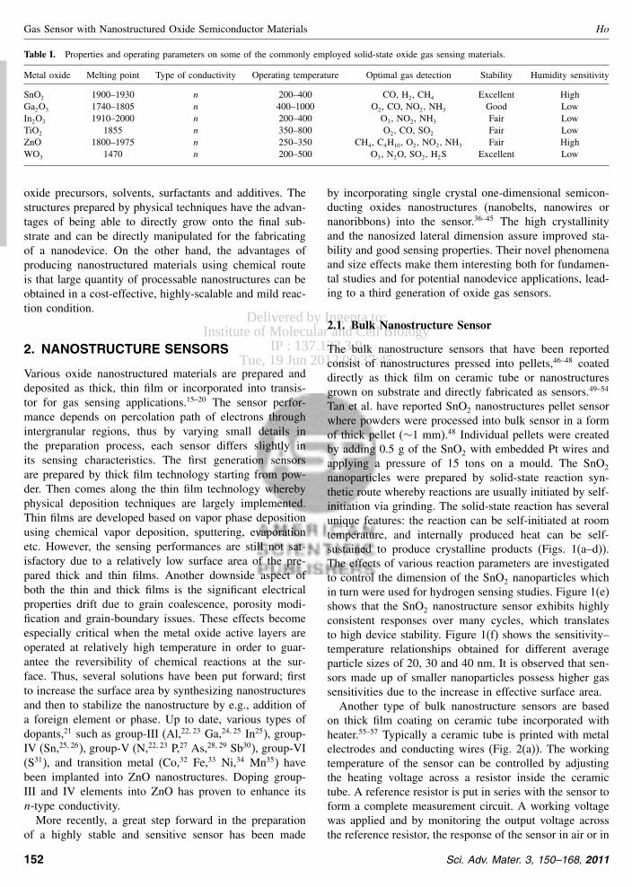
Delivered by Ingenta toInstitute of Molecular and Cell Biology
IP 13713239Tue 19 Jun 2012 003745
REVIEW
Gas Sensor with Nanostructured Oxide Semiconductor Materials Ho
Table I Properties and operating parameters on some of the commonly employed solid-state oxide gas sensing materials
Metal oxide Melting point Type of conductivity Operating temperature Optimal gas detection Stability Humidity sensitivity
SnO2 1900ndash1930 n 200ndash400 CO H2 CH4 Excellent HighGa2O3 1740ndash1805 n 400ndash1000 O2 CO NO2 NH3 Good LowIn2O3 1910ndash2000 n 200ndash400 O3 NO2 NH3 Fair LowTiO2 1855 n 350ndash800 O2 CO SO2 Fair LowZnO 1800ndash1975 n 250ndash350 CH4 C4H10 O2 NO2 NH3 Fair HighWO3 1470 n 200ndash500 O3 N2O SO2 H2S Excellent Low
oxide precursors solvents surfactants and additives Thestructures prepared by physical techniques have the advan-tages of being able to directly grow onto the final sub-strate and can be directly manipulated for the fabricatingof a nanodevice On the other hand the advantages ofproducing nanostructured materials using chemical routeis that large quantity of processable nanostructures can beobtained in a cost-effective highly-scalable and mild reac-tion condition
2 NANOSTRUCTURE SENSORS
Various oxide nanostructured materials are prepared anddeposited as thick thin film or incorporated into transis-tor for gas sensing applications15ndash20 The sensor perfor-mance depends on percolation path of electrons throughintergranular regions thus by varying small details inthe preparation process each sensor differs slightly inits sensing characteristics The first generation sensorsare prepared by thick film technology starting from pow-der Then comes along the thin film technology wherebyphysical deposition techniques are largely implementedThin films are developed based on vapor phase depositionusing chemical vapor deposition sputtering evaporationetc However the sensing performances are still not sat-isfactory due to a relatively low surface area of the pre-pared thick and thin films Another downside aspect ofboth the thin and thick films is the significant electricalproperties drift due to grain coalescence porosity modi-fication and grain-boundary issues These effects becomeespecially critical when the metal oxide active layers areoperated at relatively high temperature in order to guar-antee the reversibility of chemical reactions at the sur-face Thus several solutions have been put forward firstto increase the surface area by synthesizing nanostructuresand then to stabilize the nanostructure by eg addition ofa foreign element or phase Up to date various types ofdopants21 such as group-III (Al2223 Ga2425 In25) group-IV (Sn2526) group-V (N2223 P27 As2829 Sb30) group-VI(S31) and transition metal (Co32 Fe33 Ni34 Mn35) havebeen implanted into ZnO nanostructures Doping group-III and IV elements into ZnO has proven to enhance itsn-type conductivityMore recently a great step forward in the preparation
of a highly stable and sensitive sensor has been made
by incorporating single crystal one-dimensional semicon-ducting oxides nanostructures (nanobelts nanowires ornanoribbons) into the sensor36ndash45 The high crystallinityand the nanosized lateral dimension assure improved sta-bility and good sensing properties Their novel phenomenaand size effects make them interesting both for fundamen-tal studies and for potential nanodevice applications lead-ing to a third generation of oxide gas sensors
21 Bulk Nanostructure Sensor
The bulk nanostructure sensors that have been reportedconsist of nanostructures pressed into pellets46ndash48 coateddirectly as thick film on ceramic tube or nanostructuresgrown on substrate and directly fabricated as sensors49ndash54
Tan et al have reported SnO2 nanostructures pellet sensorwhere powders were processed into bulk sensor in a formof thick pellet (sim1 mm)48 Individual pellets were createdby adding 05 g of the SnO2 with embedded Pt wires andapplying a pressure of 15 tons on a mould The SnO2
nanoparticles were prepared by solid-state reaction syn-thetic route whereby reactions are usually initiated by self-initiation via grinding The solid-state reaction has severalunique features the reaction can be self-initiated at roomtemperature and internally produced heat can be self-sustained to produce crystalline products (Figs 1(andashd))The effects of various reaction parameters are investigatedto control the dimension of the SnO2 nanoparticles whichin turn were used for hydrogen sensing studies Figure 1(e)shows that the SnO2 nanostructure sensor exhibits highlyconsistent responses over many cycles which translatesto high device stability Figure 1(f) shows the sensitivityndashtemperature relationships obtained for different averageparticle sizes of 20 30 and 40 nm It is observed that sen-sors made up of smaller nanoparticles possess higher gassensitivities due to the increase in effective surface areaAnother type of bulk nanostructure sensors are based
on thick film coating on ceramic tube incorporated withheater55ndash57 Typically a ceramic tube is printed with metalelectrodes and conducting wires (Fig 2(a)) The workingtemperature of the sensor can be controlled by adjustingthe heating voltage across a resistor inside the ceramictube A reference resistor is put in series with the sensor toform a complete measurement circuit A working voltagewas applied and by monitoring the output voltage acrossthe reference resistor the response of the sensor in air or in
152 Sci Adv Mater 3 150ndash168 2011
Delivered by Ingenta toInstitute of Molecular and Cell Biology
IP 13713239Tue 19 Jun 2012 003745
REVIEW
Ho Gas Sensor with Nanostructured Oxide Semiconductor Materials
20 nm30 nm40 nm
(a)
(c) (d)
(b)(e)
(f)
Fig 1 SEM images of the SnO2 nanostructures obtained with variation in (andashb) precursor and (cndashd) additive concentrations (e) Typical currentresponse and (f) Sensitivityndashtemperature relationship of the bulk SnO2 nanostructure hydrogen sensor Reprinted with permission from 48 E T HTan et al Nanotechnology 19 255706 (2008) copy 2008 IOP Publishing
an analyte gas can be measured Guo et al have reportedFe2O3 porous nanorods and branched nanostructures bulksensors The nanostructures were synthesized by dehydra-tion and recrystallisation of -FeOOH precursor whichwas obtained from the hydrothermal reaction of FeCl3with urea in an aqueous system The morphology of theas-prepared nanostructures was characterized by TEM asshown in Figure 2(b) The inset shows the electron diffrac-tion pattern and ring which indicate the polycrystallinenature Figure 2(c) shows voltage response of the sensor ata working temperature of 150 C and 30 relative humid-ity It can be seen that output voltage values increasedabruptly on the injection of ethanol and then decreasedrapidly and recovered to their initial value after the testgas was released The response and recovery time of thenanostructure-based sensors were 1ndash3 and 4ndash8 s respec-tively There is also work reported on Fe2O3 nanotubeswhich show good ethanol sensing performance58
Similarly other bulk nanostructure sensor based on thickfilm coated on ceramic tube is also reported57 Homoge-neous In(OH)3 or InOOH colloidal supernatant was coatedonto a ceramic tube on which a pair of Au electrodes wasprinted After the solvent evaporation the colloidal crystalsform a thin film on the ceramic tube Then the ceramictube was annealed at 300 and 400 C for 2 h to transformIn(OH)3 or InOOH into cubic and hexagonal In2O3 respec-tively The conductance undergoes a drastic rise upon theinjection of reducing compound ethanol and drops to itsinitial value after ethanol is released These sensors showa quick response of less than 10 s and recovery time of15 s The lowest detection limit is down to 1 ppm The
response of the sensor correlates to the concentration ofthe test gas the structure and the morphology of In2O3
Another form of bulk nanostructure sensor is basedon nanowire grown and fabricated directly on the sub-strate From the viewpoint of device structure the conven-tional nanowire-based gas sensors were fabricated eitherby pick-and-place process of a single nanowire followedby making electrical contacts to individual nanowireThe device fabrication process uses expensive and timeconsuming procedures of sonication and dispersal ofnanowires on substrate with electrodes fabricated byelectron-beam lithography In this bulk nanowire sensordevice all these complicated processing steps can be elim-inated Figures 3(andashb) shows side and top-view SEMimages of ZnO nanowires grown on patterned electrodes59
Figure 3(c) shows the schematic diagram of the bulknanowire sensor device which was fabricated directly onthe growth substrate There are many nanowire-nanowirejunctions (Fig 3(d)) which act as electrical conductingpath Figure 3(e) shows the gas response as a functionof NO2 concentration at 225 C where the gas responseis directly proportional to gas concentration Figure 3(f)shows evidence of saturation at the NO2 concentrationlarger than 3 ppm This can be explained by the competi-tion between the adsorption sites versus the concentrationof target gas In a low gas concentration the availableadsorption sites on the surface of ZnO can be regardedas infinite compared with the NO2 concentration and thusthe rate-determining step might be the surface reactionbetween NO2 molecules and ZnO surface Thus surfacereactions are linearly dependent on the NO2 concentrationas long as adsorption sites are enough
Sci Adv Mater 3 150ndash168 2011 153
Delivered by Ingenta toInstitute of Molecular and Cell Biology
IP 13713239Tue 19 Jun 2012 003745
REVIEW
Gas Sensor with Nanostructured Oxide Semiconductor Materials Ho
(a)
(b)
(c)
Fig 2 (a) Schematic illustration of the gas sensor measurement system(b) TEM images of the as-synthesized Fe2O3 nanostructures (c) Real-time ethanol sensing characteristics of sensors based on the preparedFe2O3 nanostructures Reprinted with permission from [55] X L Gouet al Chem Eur J 14 5996 (2008) copy 2008 Wiley
Similarly bulk nanowire sensors were fabricateddirectly on nanowires grown on substrates60 Contactsto the multiple nanowires network were formed using ashadow mask and sputtering of AlTiAu electrodes Thesensor studies were on the time dependence of relative
resistance change of either metal-coated or uncoated net-work ZnO nanowire as the gas ambient is switched fromN2 to 500 ppm of H2 in air and then back to N2 Thehighest response is Pt coated nanowires which is followedby Pd while the other metals produce little or no changein response This is consistent with the known catalyticproperties of these metals for hydrogen dissociation Thesensors response to various gas concentrations and it candetect lt100 ppm H2 Other example of nanowire gas sen-sors which have been fabricated on Cd-Au comb-shapedinterdigitating electrodes is shown in Figures 3(gndashh)61 Thebulk nanowire sensors maintain high response to hydrogenconcentration in the range of 10 to 1000 ppm This highresponse is attributed to the highly connected network ofnanowires Similarly microtrench has been created on Sisubstrates and nanowires are grown using a thermal chem-ical vapor deposition and directly fabricated into sensor62
SnO2 nanowires are synthesized to be sufficiently long tobridge across trenched electrodes In this process compli-cated and individual alignment process is avoided and anumber of devices can be fabricated in a single processstep at a wafer scale The gas-sensing characteristics of thedeveloped sensor were significantly better when comparedto other types of NO2 sensors reported in the literatureThe sensitivity was gt150 at a NO2 concentration of 5 ppm
22 Two-Terminal Thin Film Nanostructure Sensor
Two terminal thin film sensor made up of one to fewmonolayer of nanostructures spanning across two elec-trodes are commonly fabricated The sensing device con-sists of a low-density layer of nanostructures whichare depositeddispersed onto preprepared coplanar elec-trodes Ho et al have reported on two-terminal meso-porous nanospheres thin film sensor (Fig 4(a))63 Thenanospheres (Figs 4(bndashc)) were synthesized based ona simple hydrothermal method using potassium stannatetrihydrate as a precursor in an ethanolndashdeionized watermixed solvent The parameters affecting the morphologyand porosity of the synthesized SnO2 nanostructures areinvestigated by varying various experimental conditionssuch as temperature precursor concentration and addi-tives The nanospheres grown without urea additive andat higher temperature (225 C) exhibit the highest spe-cific surface area of 1564 m2g with pore diameter of53 nm The nanospheres were diluted and dispersed inwater before drop casting a few monolayers onto the elec-trodes Figure 4(d) shows the current response graphsobtained by cycling it alternately in dry air and H2 at var-ious operating temperature It is noted that the responsetime (90 of RairndashRgas) is achieved within the first 13ndash30 min while the recovery time is 14ndash46 min depend-ing on the operating temperature of the sensor The effectof operating temperature of the reference sample on thesensor performance is investigated The responses of the
154 Sci Adv Mater 3 150ndash168 2011
Delivered by Ingenta toInstitute of Molecular and Cell Biology
IP 13713239Tue 19 Jun 2012 003745
REVIEW
Ho Gas Sensor with Nanostructured Oxide Semiconductor Materials
(c) (e)
(f)(b)
(a)
(d)
(g)
(h)
Fig 3 (a) Side and (b) top-view SEM images clearly show selective growth of ZnO nanowires on TiPt electrode (c) The schematic illustration ofZnO-nanowire air bridges over the SiO2Si substrate (d) The junction between ZnO nanowires grown on both electrodes (e) Responses of a nanowire-bridge ZnO gas sensor as a function of NO2 concentration (05ndash20 pm) at operating temperature of 225 C (f) Response versus NO2 concentrationplot which shows linear dependence in range of 05ndash3ppm (gndashh) Nanowire with interconnecting network for bulk nanowire sensing Figures 3(andashf)reprinted with permission from [59] M-W Ahn et al Sens Actuators B 138 168 (2009) copy 2009 Elsevier Limited Figures 3(gndashh) reprinted withpermission from [61] B Wang et al J Phys Chem C 112 6643 (2008) copy 2008 American Chemical Society
(a) (b) (c)
(d)
(f)
(e)
Fig 4 (a) Optical image of the fabricated sensor (bndashc) SEM images of SnO2 nanospheres synthesized at various reaction conditions (d) Responseand recovery times of the nanospheres sensor at various operating temperatures Response plot versus (e) operating temperature and (f) specific surfacearea of SnO2 nanospheres sensors Reprinted with permission from [63] S C Yeow et al Sens Actuators B 143 295 (2009) copy 2009 ElsevierLimited
Sci Adv Mater 3 150ndash168 2011 155
Delivered by Ingenta toInstitute of Molecular and Cell Biology
IP 13713239Tue 19 Jun 2012 003745
REVIEW
Gas Sensor with Nanostructured Oxide Semiconductor Materials Ho
sensor at different operating temperatures (200ndash450 C)are shown in Figure 4(e) As such a higher operatingtemperature leads to a greater change in conductance andhence greater response On the other hand desorption ofall oxygen ionic species previously adsorbed occurs at hightemperatures which explains the reduction in response asoperating temperature is increased beyond the optimumvalue Furthermore the effect of specific surface area onthe gas sensing performance is studied Figure 4(f) showsthe response plot obtained at 350 C for all the sampleswith different specific surface areas It can be observedthat it is not a linear relationship A possible explanationis that the inner surfaces of the porous nanospheres arenot fully utilized for gas detection due to the limitation ofdiffusion of the analyte gas through the nanoporesSysoev et al have reported thin film of nanoparticles
and nanowires sensor mounted on microchip64 The devicehas demonstrated an excellent performance as a gas sen-sor capable of detecting and discriminating between sev-eral reducing gases in air at a ppb level of concentra-tion Both nanoparticles film and nanowire mats weredeposited onto thermally oxidised SiO2Si substrates withPt strip electrodes and Pt meander heaters microarray TheSnO2 nanoparticles layers were deposited onto the sub-strates by spin-coating from an aqueous colloidal disper-sion of the nanoparticles (Fig 5(a)) SnO2 nanowires aredry transferred to substrate to yield one-two monolayernetwork of percolating nanowires (Fig 5(b)) Figures 5(cndashd) depict the experimental data on a long-term evolution of
(a)
(b)
(c)
(d)
Fig 5 HRTEM and SEM images of (a) SnO2 mesoporous nanoparticles layer and (b) SnO2 nanowires (c) Response and (d) resistance of thenanoparticles (open circles) and nanowires (filled circles) over time Reprinted with permission from [64] V V Sysoeva et al Sens Actuators B139 699 (2009) copy 2009 Elsevier Limited
the SnO2 nanostructures sensing characteristics toward the2-propanol vapor The response of nanowire mat to 1 ppmof 2-propanol is about sim64 The as-prepared nanoparti-cles sensor exhibits a high response of sim4times103 How-ever over 48 days the nanoparticle response drops rapidlyto 16 close to the nanowires sensor capability It hasbeen postulated that the initial high porosity nanoparti-cles allow high gas diffusion thus rendering high responseNevertheless the long-term exposure to 2-propanol vaporsat elevated operating temperature seems to facilitate sin-tering of nanoparticles Thus the two-terminal nanowiresensor is predicted to be a better conductometric gassensor with relatively high gas sensitivity and long-termstabilityOther work on two terminal sensors is based on SnO2
nanowires which were synthesized by thermal evaporationat 900 C65 The obtained nanowires were doped with pal-ladium by coating the nanowires with palladium chloride(PdCl2 and annealed at 350 C for 30 min in air in orderto decompose PdCl2 (Figs 6(andashb)) Gas sensors based onundoped 08 wt Pd-doped and 2 wt Pd-doped SnO2
nanowires were fabricated These SnO2 nanowire gas sen-sors showed a reversible response to H2 gas at operatingtemperature of 150 C (Figs 6(cndashd)) The sensor responseincreased with Pd concentration The 2 wt Pd-dopedSnO2 nanowire sensor showed a response as high as 253for 1000 ppm H2 gas at 100
C (Fig 6(d)) Pd doping hasdemonstrated to improve the sensor response and lowerthe operating temperature
156 Sci Adv Mater 3 150ndash168 2011
Delivered by Ingenta toInstitute of Molecular and Cell Biology
IP 13713239Tue 19 Jun 2012 003745
REVIEW
Ho Gas Sensor with Nanostructured Oxide Semiconductor Materials
(c)
(d)
(a) (b)
Fig 6 (andashb) TEM image of a 2 wt Pd-doped SnO2 nanowire with adiameter of 80 nm Inset shows the diffraction pattern of PdO nanopar-ticle on the nanowire Changes in the resistance of (c) undoped and(d) 2 wt Pd-doped SnO2 nanowire gas sensors upon exposure to 100200 400 800 and 1000 ppm of H2 gas Reprinted with permissionfrom [65] Y B Shen et al Sens Actuators B 135 524 (2009) copy 2009Elsevier Limited
(e)
Fig 7 (andashb) SEM images and (cndashd) IndashV curves of the single and multiple ZnO nanowire FETs respectively (e) The typical response curves ofthe single and multiple ZnO nanowire for variations of hydrogen concentration ranging from 50 to 100 ppm at 200 C Reprinted with permissionfrom [67] R Khan et al Sens Actuators B 150 389 (2010) copy 2010 Elsevier Limited
23 FET Nanostructure Sensor
In the case of field effect transistor sensor active nanowiresensor element can act as a resistive element whose resis-tance can be changed by the field-effect or charge transferprocess66ndash69 The sensing properties can be monitored byvarying the gate potential For instance Huang et al66 havereported a highly sensitive single Ga2O3 nanowire sensorwhich operates at room temperature although it is well-known fact that the Ga2O3 films sensors usually operateat high temperature of 400 to 1000 C The room temper-ature sensitivity observed here is most likely due to thegood crystallinity and ultrahigh surface-to-volume ratiosof the one-dimensional nanostructures The gas-sensingmeasurements were performed for an individual Ga2O3
nanowire device with two AuTi electrodes and the source-drain biased voltage fixed at 10 V When the individualGa2O3 nanowire is exposed to a mixed flow of ammonia(1000 ppm) and air the current is increased dramaticallyin the first 100 seconds and enhanced to about 30 timesand stabilized at sim7800 nA The Ga2O3 nanowire deviceexhibits a sensitivity of about 38 and a response time ofsim58 s in the ambient of 1000 ppm air-diluted NH3Khan et al have reported single and multiple nanowire
FET sensors67 Figures 7(a and b) show typical SEMimages of the single and multiple ZnO nanowire FETdevices70 For comparison purposes the distance betweenthe electrodes and the diameter of the ZnO nanowires werekept the same for both devices Figures 7(c and d) exhib-ited the typical electrical characteristics for the n-type sin-gle and multiple ZnO nanowire FETs respectively Themultiple nanowire devices showed greatly enhanced con-ductance due to increased number of nanowire Figure 7(e)shows the gas sensing characteristics as a function of timefor the single and multiple ZnO nanowires with varioushydrogen concentrations in the range of 50ndash100 ppm at200 C The sensor response was higher for the multiple
Sci Adv Mater 3 150ndash168 2011 157
Delivered by Ingenta toInstitute of Molecular and Cell Biology
IP 13713239Tue 19 Jun 2012 003745
REVIEW
Gas Sensor with Nanostructured Oxide Semiconductor Materials Ho
(a)
(b)
(c)
(d)
Fig 8 IndashVg curves before and after exposure to (a) 100-ppm NO2 and (b) 1 NH3 The response time of (c) 20 2 and 05 ppm NO2 and (d) 002NH3 Reprinted with permission from [68] C Li et al Appl Phys Lett 82 1613 (2003) copy 2003 American Institute of Physics
(a)
(b)
(c)
(d)
Fig 9 Schematic of (a) single and (b) multiple nanowire transistor structure where TiAu are deposited on nanowire-decorated SiSiO2 substrateas drain and source electrodes (c) IndashVg and (d) GGo versus time for the single and multi nanowire sensor device recorded at different NO2
concentrations Reprinted with permission from [72] D H Zhang et al Nano Lett 4 1919 (2004) copy 2004 American Chemical Society
158 Sci Adv Mater 3 150ndash168 2011
Delivered by Ingenta toInstitute of Molecular and Cell Biology
IP 13713239Tue 19 Jun 2012 003745
REVIEW
Ho Gas Sensor with Nanostructured Oxide Semiconductor Materials
ZnO nanowires than the response for the single ZnOnanowire over the entire range of hydrogen concentra-tion The multiple nanowires FET are made up of nano-junctions which acted as a potential barrier for electronflow The potential barrier decreased as the nanowire wasexposed to the reducing gas resulting in an increase inthe current flow The potential barrier modulation of mul-tiple nanowires was more efficient than the modulation ofthe surface depletion of the single ZnO nanowire in gassensing Therefore the potential barrier modulation in thenanojunctions caused the enhanced sensor response for themultiple nanowiresLi et al68 demonstrated the use of a single one-
dimensional nanowire FET sensor for high performanceroom temperature sensing The sensor is made up ofIn2O3 nanowires of diameter 10 nm and length 5 mwhich were placed between the source and drain elec-trodes with a silicon substrate as a back gate (Fig 8 inset)The as-fabricated In2O3 nanowire sensor devices exhib-ited typical n-type transistor characteristics The individualIn2O3 nanowire transistors sensors exhibited superior per-formance as such the sensitivity is of 106 for NO2 and 105
for NH3 which are four or five orders of magnitude betterthan results obtained from the thin-film based sensors71
Response times are as short as 5 s for 100-ppm NO2 and10 s for 1 NH3 The lowest detectable gas concentrationsare 05 ppm for NO2 and 002 for NH3
Furthermore the sensing and selectivity between dif-ferent gases can be studied by monitoring the currentdependence on the gate bias and the threshold voltageshift rendering a significant advantage over thin-film-based devices Figure 8(a) shows two currentndashgate volt-age (IndashVg) curves measured before and after exposure to100 ppm NO2 in argon with a constant source drain volt-age (Vds of minus03 V Both measurements suggest that theIn2O3 nanowires are n-type semiconductor as the con-ductance increase with gate bias There is also a pro-nounced shift in the threshold voltage from minus48 V before
(c)
Fig 10 (a) TEM of nanowires and nanobelts (b) Schematic view of device used for the in situ conductometric measurements under gas exposure andmetal deposition (c) Response of a pristine (dashed line) and Pd-functionalized (solid line) nanostructure to sequential oxygen and hydrogen pulses at473 K (top pane) and 543 K (bottom) Reprinted with permission from [73] A Kolmakov et al Nano Nano Lett 5 667 (2005) copy 2005 AmericanChemical Society
the exposure to 20 V after the exposure Adsorption ofoxidizing gases reduces the number of free electrons inthe n-type semiconductor and thus reduces the conductiv-ity Figure 8(b) shows two IndashVg curves before and afterexposing to diluted NH3 in Ar with Vds =minus03 V A largethreshold voltage shift from 248 V to 216 V is observedwith a maximum sensitivity of 105 at Vg = minus30 V ForNO2 concentrations of 20 2 and 05 ppm the responsetimes are determined to be 20 s 5 min and 10ndash12 minrespectively (Fig 8(c)) Figure 8(d) shows a response timeof about 2 min for 002 NH3 which is the lowest testedconcentration The limitation is imposed by the availabilityof highly diluted NH3 in air or argonZhang et al72 have demonstrated FET NO2 sensor down
to ppb levels based on both single and multiple In2O3
nanowires operating at room temperature as shown inschematic diagram Figures 9(a and b) Figure 9(c) showsthe conductance versus gate bias (Vg curves recorded inthe six different NO2 concentrations after exposure for20 min for single nanowire FET The threshold gate volt-age shifted rightward monotonically with the increasingNO2air concentration implying the gradual suppressionof carrier concentration of nanowire that scales linearlywith the absolute value of gate threshold As for the multinanowire FET the typical number of nanowires bridg-ing adjacent metal electrodes is estimated to be 100ndash200Figure 9(d) shows the sensing cycles of the multiwire FETdevice corresponding to NO2air concentrations of 5 1020 50 100 and 200 ppb The multiwire sensor showeda lower detection limit of 5 ppb compared to the 20 ppblimit of single nanowire sensors The room temperaturedetection limit is one of the lowest level ever reportedFurthermore selective detection of NH3 O2 CO and H2
is possible with this nanowire FET sensorKolmakov et al has demonstrated an enhanced 1-D
SnO2 nanostructure-based sensor with and without Pdnanoparticles decorated nanobelts (Fig 10(a))73 Thedeposited Pd works as catalysts for oxygen dissociation
Sci Adv Mater 3 150ndash168 2011 159
Delivered by Ingenta toInstitute of Molecular and Cell Biology
IP 13713239Tue 19 Jun 2012 003745
REVIEW
Gas Sensor with Nanostructured Oxide Semiconductor Materials Ho
Figure 10(b) shows the schematic view of device used forthe in situ conductometric FET measurements under gasexposure and metal deposition The sensing performanceof a SnO2 nanowire toward sequential oxygen and hydro-gen pulses at two different temperatures before (dashedcurves) and after (solid curves) Pd deposition is shownin Figure 10(c) Functionalizing the nanowire surface withPd leads to an enhancement in IDS response for both gasesand shorter response time Functionalizing the nanowiresurface with Pd leads to an enhancement in IDS responsefor both gases and to an increased speed of response Pdmetal nanoparticles grown on reduced n-SnO2 nanowiresand nanobelts were found to form Schottky-barrier likejunctions which locally deplete the nanostructure of elec-trons The improvements of sensitivity can be explained bythe combined ldquospillover effectrdquo of atomic oxygen formedcatalytically on the Pd particles then migrating onto thetin oxide and the back spillover effect in which weaklybound molecular oxygen migrate to the Pd and are cat-alytically dissociated Raising the temperature raises thevalue of IDS and shortens the response time of the sensorto O2 and H2 This effect is most prominent for oxygenfor which the nanostructure only becomes activated above543 K
3 DIRECTED ASSEMBLY OFNANOSTRUCTURE SENSORS
The application of nanostructures as building blocks forsensor can be achieved by implementing effective assem-bly and integration techniques to transfer the nanostructuresfrom growth substrates onto their respective device sub-strates Several methods have been developed to assembleone-dimensional nanostructures which include microflu-idic channel Langmuir-Blodgett blown bubble film self-assembled monolayers transfer printing alignment etcIn essence these approaches employ external forces toalign the nanostructures via wet or dry media In someapproaches multilayer alignment is possible while oth-ers allow selective spatial alignment in large-scale Thedevelopment of nanostructures based sensor generallyinvolves two processes First the assembly of nano-structures into highly integrated arrays with controlledorientation and spatial position second integration of inter-connects between nanostructures and the micro or macro-scopic subsystems
31 Transfer Printed Nanostructure Sensor
Transfer printing is a dry alignment technique wherebynanostructures are printed in contact or close proximityto the substrate allowing the nanostructures to be alignedin the same direction and in a predetermined densityThe nanostructures are grown on a substrate ldquostampsrdquoand then stamped ldquoprintedrdquo onto the receiving substrate
The receiving substrate can have pre deposited electrodesupon which nanostructures can be aligned The transferprinting deposition strategy has demonstrated to lead towell-defined and reproducible three-dimensional integratedcircuits structures of controlled nanowiresrsquo density andalignment over large substrate areas7475
Layer-by-layer assembly of nanowires for three-dimensional multifunctional electronics has been reportedby Javey et al74 The dry alignment process involves(i) optimized growth of designed nanowires by nanoclus-ter directed synthesis and(ii) patterned transfer of nanowires directly from ananowire growth substrate to a second device substrate viacontact printing (Figs 11(andashb))
In detail a photolithographically patterned device sub-strate is first firmly attached to a bench top and thenanowire growth substrate is placed face down in con-tact with the patterned device substrate A gentle man-ual pressure is then applied from the top followed bysliding the growth substrate by 1ndash3 mm before thegrowth substrate is removed Devices and circuits arethen fabricated on the printed arrays of nanowires usingconventional top-down lithography and metallization pro-cesses To fabricate a three-dimensional FET the con-tact printing of nanowires and device fabrication stepsare repeated several times along with the deposition ofSiO2 insulating layer in order to obtain vertically stackedelectronic layers (Figs 11(cndashd)) Another work which isalso reported by the same group is ordered arrays ofsingle-crystalline nano- and microwires of GaAs and InPwith well-controlled lengths widths and shape have beenfabricated over large areas from high quality bulk wafersby the use of traditional photolithography and anisotropicchemical wet etching75 Printing using elastomeric stampscan transfer these wire arrays to plastic substrates withexcellent retention of order and crystallographic orienta-tion of the wires Figure 11(e) shows the various printingconfiguration single to triple layers of nanowires patternsElectrical measurements on simple test structures demon-strate the high degree of mechanical flexibility of theresulting wire arrays on plastics The combination of topdown wire fabrication and transfer printing represents aneffective route to ultrahigh performance macroelectronicsystemsThe nanowires are observed to be cleanly printed
only at lithographically predefined locations FET device(Figs 14(cndashd)) The printed nanowires are aligned uni-formly across mm or larger scale with relatively highdensities (sim4 nanowirem) The monolithic integration ofindividual and parallel arrays of multifunctional and multi-layer circuits consists of up to 10 addressable vertical lay-ers This alignment methodology is applicable for the widerange of nanowire materials substrates and device designsFurthermore the simplicity and the low processing tem-perature requirement of the method makes it ideal for
160 Sci Adv Mater 3 150ndash168 2011
Delivered by Ingenta toInstitute of Molecular and Cell Biology
IP 13713239Tue 19 Jun 2012 003745
REVIEW
Ho Gas Sensor with Nanostructured Oxide Semiconductor Materials
(e)
Fig 11 Overview of 3D nanowire circuit integration (a) Contact printing of nanowire from growth substrate to prepatterned substrate (b) 3Dnanowire circuit is fabricated by the iteration of the contact printing device fabrication and separation layer deposition steps (c) Optical microscopeimage of 3D nanowire FETs (d) Dark field image shows a parallel array of nanowires aligned between source (S) drain (D) and top gate (G)electrodes Reprinted with permission from [74] A Javey et al Nano Lett 7 773 (2007) copy 2007 American Chemical Society (e) Images of singleto multiple layers of GaAs wire array which are transfer printed using elastomeric stamps Reprinted with permission from [75] Y G Sun and J ARogers Nano Lett 4 1953 (2004) copy 2004 American Chemical Society
achieving high performance three-dimensional integratedcircuitry with different functionalities in distinct layersTo demonstrate the potential of nanowire printing for
large-area sensor integration printed Si-nanowire arrayswere configured as H2 sensors P -type SiNWs were printedon Si substrates and two-terminal devices with Ni sili-cide contacts were fabricated77 The conductance of theSi nanowire array shows a strong dependence on the H2
exposure even at relatively low concentrations (250 ppm)It is worth noting that the nanowire printing method mayprovide a viable route toward the realization of electronicnoses and smart sensors capable of distinguishing chem-ical species while determining their concentrations Suchsensors may be envisioned through a large-scale integra-tion of different sensor components interfaced with signal-processing functions To achieve this goal heterogeneousassembly of nanowire materials with orthogonal sensitivityto different analytes is needed which may be achievedthrough a multistep nanowire printing process
32 Dielectrophoretic AssembledNanostructure Sensor
Dielectrophoresis (DEP) technique utilizes the dielectro-phoretic force acting on the particles to induce spatial
movement when exposed to a non uniform electric field inthe suspension medium The force depends on a numberof parameters such as the arrangement of the electrodethe frequency of the electric field and the resulting elec-tric field distribution as well as the dielectric propertiesof the particles and the surrounding medium By changingthese factors this force will pull the particle towards thehigher electric field region (positive DEP effect) or push ittowards the lower field region (negative DEP effect) DEPis a manipulation technique based on Maxwellrsquos classicalelectromagnetic field theory to allow controlled movementof particles in a controlled electric field between the presetelectrode structures The DEP technique has demonstratedthe potential for the construction of the nanosensors ornanoelectronic devices using as the nanostructured mate-rial as the building blocksJiang et al78 have reported work on manipulation of ZnO
nanorods by applying AC signals of suitable frequency andvoltage to provide non uniform electrical field on differentpatterns of electrode (Figs 12(andashb)) Similarly Li et al79
have proposed DEP assembly of nanowires onto interdigi-tated microelectrodes (Fig 12(c)) and mounted on micro-hotplate sensor platform (Fig 12(d))Template-assisted electrodeposition method and a
two-step thermal oxidation are employed Through
Sci Adv Mater 3 150ndash168 2011 161
Delivered by Ingenta toInstitute of Molecular and Cell Biology
IP 13713239Tue 19 Jun 2012 003745
REVIEW
Gas Sensor with Nanostructured Oxide Semiconductor Materials Ho
(a)
(b) (d)
(c)
Fig 12 (andashb) Low and high resolution SEM images of aligned ZnO nanowire in the interdigitated electrode array The voltage and the frequency ofthe applied electric field are 10 V and 5 kHz Reprinted with permission from [78] K W Jiang et al Sens Actuators B 134 79 (2008) copy 2008Elsevier Limited (c) Well dispersed and fairly aligned indiumtin nanowires bridged across the electrode array (d) Overview of the integrated sensorchip on micro-hotplate Reprinted with permission from [79] X P Li et al Sens Actuators B 148 404 (2010) copy 2008 Elsevier Limited
DEP(Sine waves)
Thermal andoxidationtreatment
Gas sensingmeasurement
Prefabrication of electrodes
Nanowire dispersion
Fig 13 Schematic of nanowire sensor integration nanowire suspension drop casting on interdigitated microelectrodes DEP assembly of metalnanowires alignment of nanowires on microelectrodes two-step thermal oxidation of nanowires and final integrated sensor chip The response curve ofthe various volatile organic compounds versus temperature Reprinted with permission from [80] T Jinkawa et al J Mol Catal A 155 193 (2000)copy 2008 Elsevier Limited
162 Sci Adv Mater 3 150ndash168 2011
Delivered by Ingenta toInstitute of Molecular and Cell Biology
IP 13713239Tue 19 Jun 2012 003745
REVIEW
Ho Gas Sensor with Nanostructured Oxide Semiconductor Materials
electrodeposition synthesis method one-dimensionalindium oxide tin oxide and indiumndashtin oxide nanowireswere successfully fabricated The nanowires are uniformand easy to process and assemble with good control ofchemical compositions The process flow of fabricatingnanowire sensor via DEP alignment process is shown inFigure 1380 The nanowires solution is prepared and dropcasted onto prefabricated interdigitated electrodes Thenanowires are observed to be randomly dispersed on theelectrodes The electrical field was generated by connect-ing a function generator to the interdigitated electrodeswhile a sinusoidal wave with a frequency of 5ndash6 MHzand peak-to-peak voltage of 6 V was applied during theDEP process At room temperature ethanol volatizedwithin minutes leaving nanowires aligned between theelectrode pairs Two thermal treatment processes werecarried out after the DEP assembly of nanowires to lowerthe contact resistance between the aligned nanowires andmicroelectrodes and increased the stability of the nanowireassembled First aligned metal nanowires were heated toabout 10 C below their melting points the temperaturevaried according to different material compositions Thebonding process was carried out in an inert nitrogenenvironment to prevent oxidation Next nanowires wereheated at the temperature just below the melting point ofthe respective material in an atmospheric environment for2 h The temperature was later raised to 400ndash500 C foranother 3 h to achieve full oxidation After the thermaland oxidation treatment the nanowire sensor chip wasready for electrical measurement and chemical response
ndash500
ndash400
ndash300
ndash200
ndash100
00
100
18E+10
22E+10
26E+10
30E+10
34E+10
38E+10
42E+10
0 600 1200 1800 2400 3000 3600 4200 4800
2500ppmH2
2000ppmH2
1154ppmH2
1000ppmH2
CDA CDA CDACDA
ndash350
ndash300
ndash250
ndash200
ndash150
ndash100
ndash50
00
50
100
40E+09
45E+09
50E+09
55E+09
60E+09
65E+09
70E+09
0 300 600 900 1200 1500 1800 2100 2400 2700
Time (s)
Time (s)
Res
ista
nce
(Ω)
Res
ista
nce
(Ω)
Sen
sitiv
ity (
)
Sen
sitiv
ity (
)
UV onUV on
UV off UV off
(a)
(c) (d)
(b)(e)
(f)
Fig 14 SEM images of (a) cotton textile substrate in low magnification (b) bare cotton fibres (c) ZnO nanorods-coated cotton fibres and (d) highmagnification images of ZnO nanorods on a cotton fibre Scale bar in the inset represents 100 nm Electrical responses of ZnO nanorods-on-cloth deviceto (e) various concentrations of H2 gas and (f) UV irradiation Clean dry air (CDA) was used to flush the chamber before and after each hydrogeninjection Experiments were performed in room temperature Reprinted with permission from [89] Z H Lim et al Sens Actuators B 151 121 (2010)copy 2010 Elsevier Limited
testing The sensor was investigated with different volatileorganic compounds The sensitivity of three alcohols isthe highest for methanol follow by ethanol isopropanolThese findings coincide with the number of methyl groupsin their chemical structure Two competitive dissociativereactions were proposed80 to explain the alcohol moleculesadsorbed on the oxide surface simply described as OndashHand CndashO bond-breaking processes where the former onehas a greater contribution to the resistance drop Thesensitivity order may relate to the preference of eachchemical over these two competitive reactions
4 NON-CONVENTIONAL SUBSTRATESENSOR
Technological and industrial difficulties in further minia-turization of devices have called for innovative ways toincorporate gadgets into articles of everyday life Thereare many sensors which have been fabricated on non con-ventional substrates namely the plastic textile and papersubstrate sensor The ability to fabricate sensor deviceson plastic substrates is important owing to the demandsof handheld portable consumer electronics Plastic sub-strates possess many attractive properties including bio-compatibility flexibility light weight shock resistancesoftness and transparency However plastics has low melt-ing point and they tend to deform or melt at tempera-tures of sim200 C This limits the synthesis temperatureof nanostructures directly on the plastic substrate Vari-ous ways to transfer the nanowires from donor substrate
Sci Adv Mater 3 150ndash168 2011 163
Delivered by Ingenta toInstitute of Molecular and Cell Biology
IP 13713239Tue 19 Jun 2012 003745
REVIEW
Gas Sensor with Nanostructured Oxide Semiconductor Materials Ho
to plastic substrate such as nanoimprint contact transferLangmuir Blogett etc have been developed In additionlow temperature synthesis processes have also been devel-oped to overcome this limitation Mc Alpine et al havereported plastic nanowire sensors based on Si nanowireswhich exhibit parts-per-billion sensitivity to NO2 a haz-ardous pollutant81
Another type of non conventional substrate sensor istextile Clothing is not only a necessity it also encom-passes a complete industry ranging from the down-to-earthbasics to the upmarket and chic Smart clothingtextiles arebecoming very popular in the past decade Smart textileswhich have been developed include silicon flexible skins
(b)
(a)
(d)
(c)
Source-meter
0
2E+09
4E+09
6E+09
8E+09
1E+10
12E+10
14E+10
16E+10
18E+10
I-V 1 I-V 2 I-V 3 I-V 4 I-V 5 Average
Res
ista
nce
(Ω)
Before After
(e)
(f)
(g)
Fig 15 SEM images of (a) low resolution ZnO-nanorods-coated textile with selected area (circled in red) for subsequent studies (b) the selected ZnOnanorods-coated yarns before stretching twisting and sonication (c) the same yarns after repeated stretching and twisting and (d) 5 minutes of watersonification (e) Schematic diagram of the electro-mechanical testing and (f) electrical properties before and after each stretching and twisting cycle(g) Electrical measurement of ZnO nanorods-on-cloth device while subjected to controlled stress cycles with a mechanical testing system Reprintedwith permission from [89] Z H Lim et al Sens Actuators B 151 121 (2010) copy 2010 Elsevier Limited
and organic transistors on textile fibers8283 Another type ofthe smart sensing textiles which uses piezo-resistive prop-erties has been developed The approach for fabricating thefabrics was to coat a thin layer of piezo-resistive materialssuch as polypyrrole or a mixture of rubbers and carbonson conventional fabrics to form fabric-based sensors84ndash86
The function of the developed sensors is similar to that offlexible strain gauges which can measure strains when theyare subjected to a tensile stress Other innovations whichare not actively explored are textiles which can detectenvironmental conditions which then react and adapt toenvironmental changes Furthermore smart textiles can bemade to measure and monitor the physiological conditions
164 Sci Adv Mater 3 150ndash168 2011
Delivered by Ingenta toInstitute of Molecular and Cell Biology
IP 13713239Tue 19 Jun 2012 003745
REVIEW
Ho Gas Sensor with Nanostructured Oxide Semiconductor Materials
of the wearer eg perspiration heartbeat etc Thus they canbe applied various healthcare systems
41 Textile Sensor
While the development of wearable devices has beenreported the incorporation of nano-materials into thedesigns has not been well explored In addition problemssuch as complex process mass production washabilityand wearing comforts needs to be well addressed The easeof synthesizing ZnO nanowires or nanorods on almost anysubstrates welcomes large-scale incorporation on textileZnO nano-structures are believed to be non-toxic and bio-safe87 allowing their direct usage in daily applicationsWhile the use of nano-materials in daily human activitiesraised questions on its potential health risks there is todate no in vivo evidence of toxicity of nano-particulateZnO88
29 nm
5 nm
1 μm1 μm
2 nm 5 μm
15Endash03
16Endash03
17Endash03
18Endash03
Time (s)
on off
1000 ppm
(a)
(c) (d)(f)
(b) (e)
15Endash03
16Endash03
16Endash03
17Endash03
17Endash03
18Endash03
18Endash03
150 250 350 450 550 650 0 150 300 450 600 750 900
Time (s)
Cur
rent
(m
A)
Cur
rent
(m
A)
on off
2000 ppm1500 ppm
1000 ppm2500 ppm
(g) (h)
Fig 16 (andashb) Low and (cndashd) high resolution TEM images of the nanobelts (e) Image of nanobelts sheet made without any addition of binder orreinforcement chemicals (f) Cross-sectional SEM image of the nanobelts sheet Current response of the sensor at (g) varying and (h) same ppm H2
concentration Reprinted with permission from [90] S Bela et al J Phys D Appl Phys 43 35401 (2010) copy 2010 Institute of Physics
SEM images of the textile and nanorods displayed inFigures 14(andashd) show radially oriented nanorods (diametersim80 nm) with hexagonal cross-section grown along thecylindrical fibres (diameter sim15 m)89 Length of thenanorods is sim1 m The nanorods form a uniform anddense coverage around entire lengths of the fibres to forma cross-linked semi-conductive textileThe conductive textile shows excellent multiple sens-
ing (gas and optical) performances at room temperature asshown in Figures 14(e) and (f) respectively In the presenceof hydrogen gas chemisorbed oxygen ions are reducedto release electrons to the conduction band of the ZnOsurface resulting in an increase in conductivity In addi-tion the reduction reaction decreases the surface densityof the oxygen adsorbate leading to a reduction in thewidth of the depletion region and the height of the sur-face potential barrier thus resulting in the decrease in theresistance of the sensor The mechanism for UV sensing
Sci Adv Mater 3 150ndash168 2011 165
Delivered by Ingenta toInstitute of Molecular and Cell Biology
IP 13713239Tue 19 Jun 2012 003745
REVIEW
Gas Sensor with Nanostructured Oxide Semiconductor Materials Ho
is similar to that of hydrogen sensing with holes fromthe photo-generated electronndashhole pairs playing the role ofremoving the adsorbed oxygen molecules insteadA notable feature of the ZnO nanorods-coated textile
device is its fine morphological and electrical stabilityunder multiple stress and washing cycles A critical chal-lenge of semi-conductive yarns and textile is its durabil-ity and constancy of electrical performance SEM analyses(Figs 15(andashd)) of the nanorods -on-cloth before and afterstretching twisting and ashing cycles show no cracks ordelamination of the nanorods from the fibres respectivelyFigure 15(e) shows a schematic of the electro-mechanicaltesting Electrical characterisations made before and aftereach stretching and twisting cycle (Fig 15(f)) show goodelectrical stability We further perform electrical conduc-tivity measurements while stretching and relaxing the tex-tile device in a controlled manner The semiconductingtextile exhibits a higher conductivity when stretched dueto tighter packing (increased contact junctions) of the ZnOnanorods-coated fibers Figure 15(g) shows the variation ofcurrent through the textile device as it underwent repeatedcycles of stress and relaxation When the stress is releasedconductivity falls and stabilises to the original state Againthe morphology of the nanorods-on-textile suffered nocracks of delamination or noticeable degradation after theelectromechanical testing
42 Free Standing Sheet Sensor
Another non conventional sensor substrate is a free stand-ing sheet of nanowire paper The nanostructures are tobe produced in gram quantities so that it can be easilymade into nanostructured paper sheet The thickness ofthe nanostructures sheet can be tuned according to theamount of nanostructures used After the filtering wascompleted a sheet of nanostructures was formed by sand-wiching between a metal calender which was pressed andheated to ensure the nanowires are well dried and bondedtogether to form the free-standing paperBela et al have been reported synthesis of hybrid
titanate and titania nanobelts (Figs 16(andashd)) in a large-scale quantity for gas sensing applications90 The nanobeltsare synthesized from TiO2 powder based on hydrolysis andion exchange of NaOH base and HCl acid respectivelySheets of as-synthesized nanobelts are used for electricaland gas sensing measurements Figure 16(e) shows thewhite nanobelts sheet made without any addition of binderor reinforcement chemicals Cross-sectional SEM image ofFigure 16(f) shows that the nanobelts sheet has a thicknessof sim15 m Figures 16(g and h) show the current responseof the sensor at varying and same ppm H2 concentra-tions respectively The measurements were conducted at anoperating temperature of 300 C From the graphs it is evi-dent that the introduction of hydrogen causes the resistanceof the sensor to reduce because of the injection of electrons
onto the surface of the metal-oxide nanostructures therebyimproving the conductivity of the bulk sensing capabili-ties The resistance increases as the concentration of H2 isvaried from 2500 to 1000 ppm The response time (90of Rair minusRgas is achieved within the first 40ndash50 s whilethe recovery time is 10ndash12 min From the Figure 7(c) itwas observed that the sensing response was rather stableand reversible In oxidizing atmosphere of 300 C ambi-ent oxygen is adsorbed on the surface of nanobelts mostlikely with a negative charge Subsequently with the intro-duction of a reducing H2 gas it reacts with the negativelycharged surface oxygen and decreases the resistance bythe injection of electron
5 CONCLUSIONS
There is an immense technological and scientific potentialsof nanostructured materials in nanodevice applicationsand already numerous nanomaterial based sensors usingvarious materials have been reported These oxide materi-als can be synthesized by various synthetic routes whichinclude both physical and chemical methods The poten-tial application of these nanostructures as sensor dependsgreatly on the ability to precisely control their dimensionchemical composition surface property phase purity andcrystal structure Sensor of various configurations bulktwo-terminal and FET device have been fabricated Theintegrability of the nanostructure sensor into microelec-tronic fabrication technology is an issue that needs tobe addressed Various ways to assemble nanowires so asto ease the device fabrication process have been devel-oped The recent advances in assembling larger and morecomplex nanowire sensor arrays and integrating them intonanoscale electronics can lead to exquisite sensor sys-tem performances These sensory systems can sensitivelytransduce gaschemicalbiological binding events into elec-tronicdigital signals which promise a sophisticated nano-electronics sensing system
6 FUTURE DIRECTIONS
Although nanomaterial based sensors are expected to out-perform their bulk component there are still many issuesand parameters to be studied and addressed Parameters tobe explored include structural and composition tuning aswell as doping and functionalization of surfaces to increaseselectivity sensitivity and materials integrity for long-termstability Other parameters such as limits of detection lim-its of quantification dynamic range response and recov-ery times and lifetime have to be studied and improvedas well The long-term reliability of a sensor is impor-tant since progressive drifts in the characteristics andorresponses of the sensors affect accurate testing and analy-sis The drift of the sensors are frequently related to highworking temperatures and exposure to chemically active
166 Sci Adv Mater 3 150ndash168 2011
Delivered by Ingenta toInstitute of Molecular and Cell Biology
IP 13713239Tue 19 Jun 2012 003745
REVIEW
Ho Gas Sensor with Nanostructured Oxide Semiconductor Materials
ambient gas Many other issues include aging grain-sizegrowth poisoning due to unknown chemical species dif-fusion processes within the device etc are to be addressedas wellThe future direction of the solid-state gas sensor is
towards integrated wirelessremote multi-purpose sens-ing high selectivity recognition of a specific biological orchemical species with ldquoelectronic-nose-tonguerdquo capabili-ties In addition development of miniaturized analyticalsensor which can be integrated in-line orand as standaloneportable sensors is paramount for industrial applicationsThe sensors can further be refined into a network of sensorarrays providing rapid screening monitoring and reportingsystem The data are collected in a database and form partof a feedback guidance system to the control algorithm inindustrial processes
Acknowledgments The work is supported by NationalUniversity of Singapore grant R-263-000-532-112Images used for the cover page are kindly contributed byZ H Lee and M Kevin multidisciplinary laboratory
References and Notes
1 D James S M Scott Z Ali and W T OrsquoHare Microchim Acta149 1 (2005)
2 C-D Kohlin Nanoelectronics and Information Technology editedby R Waser Wiley-VCH Berlin (2005) p 851
3 M E Franke T J Koplin and U Simon Small 2 36 (2006)4 A Kolmakov and M Moskovits Annu Rev Mater Res 34 151
(2004)5 A Mandelis and C Christofides Physics Chemistry and Technology
of Solid State Gas Sensor Devices Wiley-Interscience New York(1993)
6 P T Moseley Sens Actuators B 6 149 (1992)7 N M White and J D Turner Meas Sci Technol 8 1 (1997)8 D Kohl J Phys D 34 R125 (2001)9 N Pinna G Neri M Antonietti and M Niederberger Angew
Chem Int Ed 43 4345 (2004)10 L P Sun L H Huo H Zhao S Gao and J G Zhao Sens Actu-
ators B 114 387 (2006)11 Z F Liu T Yamazaki Y B Shen T Kikuta N Nakatani and
Y X Li Sens Actuators B 129 666 (2008)12 C S Rout A R Raju A Govindaraj and C N R Rao J Nanosci
Nanotechnol 7 1923 (2007)13 M S Arnold P Avouris Z W Pan and Z L Wang J Phys
Chem B 107 659 (2003)14 I Jimenez I M A Centeno R Scotti F Morazzoni A Cornet
and J R Morante J electrochem Soc 150 H72 (2003)15 S Semancik and R E Cavicchi Thin Solid Films 206 81 (1991)16 N S Baik G Sakai N Miura and N Yamazoe Sens Actuators B
63 74 (2000)17 M Ivanovskaya P Bogdanov G Faglia and G Sberveglieri Sens
Actuators B 68 344 (2000)18 K Ihokura and I Watson The Stannic Oxide Gas Sensormdash
Principles and Applications CRC Press Boa Raton (1994)19 K D Schierbaum U Weimar and W Gopel Sens Actuators B
7 1 (1992)20 G Korotcenkov Sens Actuators B 121 664 (2007)21 J G Lu P C Chang and Z Y Fan Mater Sci Eng 52 49 (2006)22 T Yamamoto and H Katayama-Yoshida Jpn J Appl Phys
38 L166 (1999)
23 J G Lu L P Zhu Z Z Ye F Zhuge B H Zhao D W MaL Wang and J Y Huang J Mater Sci 41 467 (2006)
24 J Zhong S Muthukumar Y Chen Y Lu H M Ng W Jiang andE L Garfunkel Appl Phys Lett 83 3401 (2003)
25 S Y Bae C W Na J H Kang and J Park J Phys Chem B109 2526 (2005)
26 S Y Li P Lin C Y Lee T Y Tseng and C J Huang J Phys DAppl Phys 37 2274 (2004)
27 D K Hwang H S Kim J H Lim J Y Oh J H Yang S J ParkK K Kim D C Look and Y S Park Appl Phys Lett 86 151917(2005)
28 W Lee M C Jeong S W Joo and J M Myoung Nanotechnology16 764 (2005)
29 W Lee M C Jeong and J M Myoung Appl Phys Lett 85 6167(2004)
30 D W Zeng C S Xie B L Zhu R Jiang X Chen W L SongJ B Wang and J Shi J Cryst Growth 266 511 (2004)
31 G Z Shen J H Cho J K Yoo G C Yi and C J Lee J PhysChem B 109 5491 (2005)
32 J B Cui and U J Gibson Appl Phys Lett 87 133108 (2005)33 C X Xu X W Sun Z L Dong M B Yu Y Z Xiong and J S
Chen Appl Phys Lett 86 173110 (2005)34 D A Schwartz K R Kittilstved and D R Gamelin Appl Phys
Lett 85 1395 (2004)35 C Ronning P X Gao Y Ding Z L Wang and D Schwen Appl
Phys Lett 84 783 (2004)36 A J Mieszawska R Jalilian G U Sumanasekera and F P
Zamborini Small 3 722 (2007)37 B Zhu K Li S Zhang S Wu and W Huang Prog Chem 20 48
(2008)38 J X Wang S S Xie and W Zhou MRS Bull 32 123 (2007)39 W Lu and C M Lieber J Phys D-Appl Phys 39 R387
(2006)40 X Wang and Y D Li Inorganic Chemistry 45 7522 (2006)41 Y Shen T Yamazaki Z Liu D Meng T Kikuta N Nakatani
M Saito and M Mori Sens Actuators B 135 524 (2009)42 A Kolmakov Y Zhang G Cheng and M Moskovits Adv Mater
15 997 (2003)43 X T Zhou J Q Hu C P Li D D D Ma C S Lee and S T
Lee Chem Phys Lett 369 220 (2003)44 T-J Hsueh C-L Hsu S-J Chang and I-C Chen Sens Actua-
tors B 126 473 (2007)45 Q Wan Q H Li Y J Chen T H Wang X L He J P Li and
C L Lin Appl Phys Lett 84 3654 (2004)46 G J Li X H Zhang and S Kawi Sens Actuators B 60 64 (1999)47 G J Li and S Kawi Talanta 45 759 (1998)48 E T H Tan G W Ho A S W Wong S Kawi and A T S Wee
Nanotechnology 19 255706 (2008)49 S Luo G Fu H Chen and Y Zhang Mater Chem Phys 109 541
(2008)50 C Y Wang M Ali T Kups C C Roehlig V Cimalla T Stauden
and O Ambacher Sens Actuators B 130 589 (2008)51 J Ahmed S Vaidya T Ahmad P Sujatha Devi D Das and A K
Ashok Mater Res Bull 43 264 (2008)52 J Kaur R Kumar and M C Bhatnagar Sens Actuators B
126 478 (2007)53 D Lutic M Strand A Lloyd-Spetz K Buchholt E Ieva P O
Kall and M Sanati Top Cata 45 105 (2007)54 A Teleki S E Pratsinis K Kalyanasundaram and P I Gouma
Sens Actuators B 119 683 (2006)55 X L Gou G X Wang X Y Kong D Wexler J Horvat J Yang
and J Park Chem Eur J 14 5996 (2008)56 X Feng Z J Li P Y Wang and Y F Zhou J Mat Sci 40 6597
(2005)57 J Chen L Xu W Li and X Gou Adv Mater 17 582 (2005)58 Z B Zhuang Q Peng J F Liu X Wang and Y D Li Inorg
Chem 46 5179 (2007)
Sci Adv Mater 3 150ndash168 2011 167
Delivered by Ingenta toInstitute of Molecular and Cell Biology
IP 13713239Tue 19 Jun 2012 003745
REVIEW
Gas Sensor with Nanostructured Oxide Semiconductor Materials Ho
59 M-W Ahn K-S Park J-H Heo D-W Kim K J Choi and J-GPark Sens Actuators B 138 168 (2009)
60 H T Wang B S Kang F Ren L C Tien P W Sadik D PNorton S J Pearton and J Lin Appl Phys A 81 1117 (2005)
61 B Wang L F Zhu Y H Yang N S Xu and G W Yang J PhysChem C 112 6643 (2008)
62 T H Jung S-I Kwon J-H Park D-G Lim Y-J Choi and J-GPark Appl Phys A 91 707 (2008)
63 S C Yeow W L Ong A S W Wong and G W Ho Sens Actu-ators B 143 295 (2009)
64 V V Sysoeva T Schneiderb J Goschnickb I KiselevbW Habichtb H Hahnb E Strelcovc and A Kolmakov Sens Actu-ators B 139 699 (2009)
65 Y B Shen T Yamazaki Z F Liu D Meng T Kikuta N NakataniM Saito and M Mori Sens Actuators B 135 524 (2009)
66 Y Huang S Yue Z Wang Q Wang C Shi Z Xu X D BaiC Tang and C Gu J Phys Chem B 110 796 (2006)
67 R Khan H-W Ra J T Kim W S Jang D Sharma and Y HIm Sens Actuators B 150 389 (2010)
68 C Li D H Zhang X L Liu S Han T Tang J Han and C ZhouAppl Phys Lett 82 1613 (2003)
69 Z Fan and J G Lu Appl Phys Lett 86 123510 (2005)70 Z Y Fan D W Wang P C Chang W Y Tseng and J G Lu
Appl Phys Lett 85 5923 (2004)71 M Liess Thin Solid Films 410 183 (2002)72 D H Zhang Z Q Liu C Li T Tang X L Liu S Han B Lei
and C W Zhou Nano Lett 4 1919 (2004)73 A Kolmakov D O Klenov Y Lilach S Stemmer and
M Moskovits Nano Lett 5 667 (2005)74 A Javey S W Nam R S Friedman H Yan and C M Lieber
Nano Lett 7 773 (2007)75 Y G Sun and J A Rogers Nano Lett 4 1953 (2004)
76 Z Fan J C Ho Z A Jacobson R Yerushalmi R L AlleyH Razavi and A Javey Nano Lett 8 20 (2008)
77 Z Y Fan J C Ho T Takahashi R Yerushalmi K Takei A CFord Y-L Chueh and A Javey Adv Mater 21 3730 (2009)
78 K W Jiang W J Liu L J Wan and J Zhang Sens Actuators B134 79 (2008)
79 X P Li E China H W Sun P Kurup and Z Y Gu Sens Actu-ators B 148 404 (2010)
80 T Jinkawa G Sakai J Tamaki N Miura and N Yamazoe J MolCatal A 155 193 (2000)
81 M C McAlpine H Ahmad D W Wang and J R Heath NatMater 6 379 (2007)
82 R B Katragadda and Y Xu A Novel Intelligent Textile TechnologyBased on Silicon Flexible Skins Electrical and Computer Engineer-ing Wayne State University Detroit Michigan USA ISWC (2005)pp 78ndash81
83 J B Lee and V Subramanian IEEE Trans Electron Devices 62 269(2005)
84 R Wijesiriwardana K Mitcham and T Dias Fibre-meshed trans-ducers based real time wearable physiological information moni-toring system Proceedings of the 8th International Symposium onWearable Computers ISWCrsquo04 (2004) pp 40ndash47
85 R Wijesiriwardana IEEE Sens J 6 571 (2006)86 E P Scilingo F Lorussi A Mazzoldi and D De Rossi Sens J
IEEE 3 460 (2003)87 J Zhou N Xu and Z L Wang Adv Mater 18 2432 (2006)88 G J Nohynek E K Dudour and M S Roberts Nanotechnology
21 136 (2008)89 Z H Lim Z X Chia M Kevin A S W Wong and G W Ho
Sens Actuators B 151 121 (2010)90 S Bela A S W Wong and G W Ho J Phys D Appl Phys
43 35401 (2010)
Received 4 November 2010 Accepted 20 January 2011
168 Sci Adv Mater 3 150ndash168 2011

Delivered by Ingenta toInstitute of Molecular and Cell Biology
IP 13713239Tue 19 Jun 2012 003745
REVIEW
Ho Gas Sensor with Nanostructured Oxide Semiconductor Materials
20 nm30 nm40 nm
(a)
(c) (d)
(b)(e)
(f)
Fig 1 SEM images of the SnO2 nanostructures obtained with variation in (andashb) precursor and (cndashd) additive concentrations (e) Typical currentresponse and (f) Sensitivityndashtemperature relationship of the bulk SnO2 nanostructure hydrogen sensor Reprinted with permission from 48 E T HTan et al Nanotechnology 19 255706 (2008) copy 2008 IOP Publishing
an analyte gas can be measured Guo et al have reportedFe2O3 porous nanorods and branched nanostructures bulksensors The nanostructures were synthesized by dehydra-tion and recrystallisation of -FeOOH precursor whichwas obtained from the hydrothermal reaction of FeCl3with urea in an aqueous system The morphology of theas-prepared nanostructures was characterized by TEM asshown in Figure 2(b) The inset shows the electron diffrac-tion pattern and ring which indicate the polycrystallinenature Figure 2(c) shows voltage response of the sensor ata working temperature of 150 C and 30 relative humid-ity It can be seen that output voltage values increasedabruptly on the injection of ethanol and then decreasedrapidly and recovered to their initial value after the testgas was released The response and recovery time of thenanostructure-based sensors were 1ndash3 and 4ndash8 s respec-tively There is also work reported on Fe2O3 nanotubeswhich show good ethanol sensing performance58
Similarly other bulk nanostructure sensor based on thickfilm coated on ceramic tube is also reported57 Homoge-neous In(OH)3 or InOOH colloidal supernatant was coatedonto a ceramic tube on which a pair of Au electrodes wasprinted After the solvent evaporation the colloidal crystalsform a thin film on the ceramic tube Then the ceramictube was annealed at 300 and 400 C for 2 h to transformIn(OH)3 or InOOH into cubic and hexagonal In2O3 respec-tively The conductance undergoes a drastic rise upon theinjection of reducing compound ethanol and drops to itsinitial value after ethanol is released These sensors showa quick response of less than 10 s and recovery time of15 s The lowest detection limit is down to 1 ppm The
response of the sensor correlates to the concentration ofthe test gas the structure and the morphology of In2O3
Another form of bulk nanostructure sensor is basedon nanowire grown and fabricated directly on the sub-strate From the viewpoint of device structure the conven-tional nanowire-based gas sensors were fabricated eitherby pick-and-place process of a single nanowire followedby making electrical contacts to individual nanowireThe device fabrication process uses expensive and timeconsuming procedures of sonication and dispersal ofnanowires on substrate with electrodes fabricated byelectron-beam lithography In this bulk nanowire sensordevice all these complicated processing steps can be elim-inated Figures 3(andashb) shows side and top-view SEMimages of ZnO nanowires grown on patterned electrodes59
Figure 3(c) shows the schematic diagram of the bulknanowire sensor device which was fabricated directly onthe growth substrate There are many nanowire-nanowirejunctions (Fig 3(d)) which act as electrical conductingpath Figure 3(e) shows the gas response as a functionof NO2 concentration at 225 C where the gas responseis directly proportional to gas concentration Figure 3(f)shows evidence of saturation at the NO2 concentrationlarger than 3 ppm This can be explained by the competi-tion between the adsorption sites versus the concentrationof target gas In a low gas concentration the availableadsorption sites on the surface of ZnO can be regardedas infinite compared with the NO2 concentration and thusthe rate-determining step might be the surface reactionbetween NO2 molecules and ZnO surface Thus surfacereactions are linearly dependent on the NO2 concentrationas long as adsorption sites are enough
Sci Adv Mater 3 150ndash168 2011 153
Delivered by Ingenta toInstitute of Molecular and Cell Biology
IP 13713239Tue 19 Jun 2012 003745
REVIEW
Gas Sensor with Nanostructured Oxide Semiconductor Materials Ho
(a)
(b)
(c)
Fig 2 (a) Schematic illustration of the gas sensor measurement system(b) TEM images of the as-synthesized Fe2O3 nanostructures (c) Real-time ethanol sensing characteristics of sensors based on the preparedFe2O3 nanostructures Reprinted with permission from [55] X L Gouet al Chem Eur J 14 5996 (2008) copy 2008 Wiley
Similarly bulk nanowire sensors were fabricateddirectly on nanowires grown on substrates60 Contactsto the multiple nanowires network were formed using ashadow mask and sputtering of AlTiAu electrodes Thesensor studies were on the time dependence of relative
resistance change of either metal-coated or uncoated net-work ZnO nanowire as the gas ambient is switched fromN2 to 500 ppm of H2 in air and then back to N2 Thehighest response is Pt coated nanowires which is followedby Pd while the other metals produce little or no changein response This is consistent with the known catalyticproperties of these metals for hydrogen dissociation Thesensors response to various gas concentrations and it candetect lt100 ppm H2 Other example of nanowire gas sen-sors which have been fabricated on Cd-Au comb-shapedinterdigitating electrodes is shown in Figures 3(gndashh)61 Thebulk nanowire sensors maintain high response to hydrogenconcentration in the range of 10 to 1000 ppm This highresponse is attributed to the highly connected network ofnanowires Similarly microtrench has been created on Sisubstrates and nanowires are grown using a thermal chem-ical vapor deposition and directly fabricated into sensor62
SnO2 nanowires are synthesized to be sufficiently long tobridge across trenched electrodes In this process compli-cated and individual alignment process is avoided and anumber of devices can be fabricated in a single processstep at a wafer scale The gas-sensing characteristics of thedeveloped sensor were significantly better when comparedto other types of NO2 sensors reported in the literatureThe sensitivity was gt150 at a NO2 concentration of 5 ppm
22 Two-Terminal Thin Film Nanostructure Sensor
Two terminal thin film sensor made up of one to fewmonolayer of nanostructures spanning across two elec-trodes are commonly fabricated The sensing device con-sists of a low-density layer of nanostructures whichare depositeddispersed onto preprepared coplanar elec-trodes Ho et al have reported on two-terminal meso-porous nanospheres thin film sensor (Fig 4(a))63 Thenanospheres (Figs 4(bndashc)) were synthesized based ona simple hydrothermal method using potassium stannatetrihydrate as a precursor in an ethanolndashdeionized watermixed solvent The parameters affecting the morphologyand porosity of the synthesized SnO2 nanostructures areinvestigated by varying various experimental conditionssuch as temperature precursor concentration and addi-tives The nanospheres grown without urea additive andat higher temperature (225 C) exhibit the highest spe-cific surface area of 1564 m2g with pore diameter of53 nm The nanospheres were diluted and dispersed inwater before drop casting a few monolayers onto the elec-trodes Figure 4(d) shows the current response graphsobtained by cycling it alternately in dry air and H2 at var-ious operating temperature It is noted that the responsetime (90 of RairndashRgas) is achieved within the first 13ndash30 min while the recovery time is 14ndash46 min depend-ing on the operating temperature of the sensor The effectof operating temperature of the reference sample on thesensor performance is investigated The responses of the
154 Sci Adv Mater 3 150ndash168 2011
Delivered by Ingenta toInstitute of Molecular and Cell Biology
IP 13713239Tue 19 Jun 2012 003745
REVIEW
Ho Gas Sensor with Nanostructured Oxide Semiconductor Materials
(c) (e)
(f)(b)
(a)
(d)
(g)
(h)
Fig 3 (a) Side and (b) top-view SEM images clearly show selective growth of ZnO nanowires on TiPt electrode (c) The schematic illustration ofZnO-nanowire air bridges over the SiO2Si substrate (d) The junction between ZnO nanowires grown on both electrodes (e) Responses of a nanowire-bridge ZnO gas sensor as a function of NO2 concentration (05ndash20 pm) at operating temperature of 225 C (f) Response versus NO2 concentrationplot which shows linear dependence in range of 05ndash3ppm (gndashh) Nanowire with interconnecting network for bulk nanowire sensing Figures 3(andashf)reprinted with permission from [59] M-W Ahn et al Sens Actuators B 138 168 (2009) copy 2009 Elsevier Limited Figures 3(gndashh) reprinted withpermission from [61] B Wang et al J Phys Chem C 112 6643 (2008) copy 2008 American Chemical Society
(a) (b) (c)
(d)
(f)
(e)
Fig 4 (a) Optical image of the fabricated sensor (bndashc) SEM images of SnO2 nanospheres synthesized at various reaction conditions (d) Responseand recovery times of the nanospheres sensor at various operating temperatures Response plot versus (e) operating temperature and (f) specific surfacearea of SnO2 nanospheres sensors Reprinted with permission from [63] S C Yeow et al Sens Actuators B 143 295 (2009) copy 2009 ElsevierLimited
Sci Adv Mater 3 150ndash168 2011 155
Delivered by Ingenta toInstitute of Molecular and Cell Biology
IP 13713239Tue 19 Jun 2012 003745
REVIEW
Gas Sensor with Nanostructured Oxide Semiconductor Materials Ho
sensor at different operating temperatures (200ndash450 C)are shown in Figure 4(e) As such a higher operatingtemperature leads to a greater change in conductance andhence greater response On the other hand desorption ofall oxygen ionic species previously adsorbed occurs at hightemperatures which explains the reduction in response asoperating temperature is increased beyond the optimumvalue Furthermore the effect of specific surface area onthe gas sensing performance is studied Figure 4(f) showsthe response plot obtained at 350 C for all the sampleswith different specific surface areas It can be observedthat it is not a linear relationship A possible explanationis that the inner surfaces of the porous nanospheres arenot fully utilized for gas detection due to the limitation ofdiffusion of the analyte gas through the nanoporesSysoev et al have reported thin film of nanoparticles
and nanowires sensor mounted on microchip64 The devicehas demonstrated an excellent performance as a gas sen-sor capable of detecting and discriminating between sev-eral reducing gases in air at a ppb level of concentra-tion Both nanoparticles film and nanowire mats weredeposited onto thermally oxidised SiO2Si substrates withPt strip electrodes and Pt meander heaters microarray TheSnO2 nanoparticles layers were deposited onto the sub-strates by spin-coating from an aqueous colloidal disper-sion of the nanoparticles (Fig 5(a)) SnO2 nanowires aredry transferred to substrate to yield one-two monolayernetwork of percolating nanowires (Fig 5(b)) Figures 5(cndashd) depict the experimental data on a long-term evolution of
(a)
(b)
(c)
(d)
Fig 5 HRTEM and SEM images of (a) SnO2 mesoporous nanoparticles layer and (b) SnO2 nanowires (c) Response and (d) resistance of thenanoparticles (open circles) and nanowires (filled circles) over time Reprinted with permission from [64] V V Sysoeva et al Sens Actuators B139 699 (2009) copy 2009 Elsevier Limited
the SnO2 nanostructures sensing characteristics toward the2-propanol vapor The response of nanowire mat to 1 ppmof 2-propanol is about sim64 The as-prepared nanoparti-cles sensor exhibits a high response of sim4times103 How-ever over 48 days the nanoparticle response drops rapidlyto 16 close to the nanowires sensor capability It hasbeen postulated that the initial high porosity nanoparti-cles allow high gas diffusion thus rendering high responseNevertheless the long-term exposure to 2-propanol vaporsat elevated operating temperature seems to facilitate sin-tering of nanoparticles Thus the two-terminal nanowiresensor is predicted to be a better conductometric gassensor with relatively high gas sensitivity and long-termstabilityOther work on two terminal sensors is based on SnO2
nanowires which were synthesized by thermal evaporationat 900 C65 The obtained nanowires were doped with pal-ladium by coating the nanowires with palladium chloride(PdCl2 and annealed at 350 C for 30 min in air in orderto decompose PdCl2 (Figs 6(andashb)) Gas sensors based onundoped 08 wt Pd-doped and 2 wt Pd-doped SnO2
nanowires were fabricated These SnO2 nanowire gas sen-sors showed a reversible response to H2 gas at operatingtemperature of 150 C (Figs 6(cndashd)) The sensor responseincreased with Pd concentration The 2 wt Pd-dopedSnO2 nanowire sensor showed a response as high as 253for 1000 ppm H2 gas at 100
C (Fig 6(d)) Pd doping hasdemonstrated to improve the sensor response and lowerthe operating temperature
156 Sci Adv Mater 3 150ndash168 2011
Delivered by Ingenta toInstitute of Molecular and Cell Biology
IP 13713239Tue 19 Jun 2012 003745
REVIEW
Ho Gas Sensor with Nanostructured Oxide Semiconductor Materials
(c)
(d)
(a) (b)
Fig 6 (andashb) TEM image of a 2 wt Pd-doped SnO2 nanowire with adiameter of 80 nm Inset shows the diffraction pattern of PdO nanopar-ticle on the nanowire Changes in the resistance of (c) undoped and(d) 2 wt Pd-doped SnO2 nanowire gas sensors upon exposure to 100200 400 800 and 1000 ppm of H2 gas Reprinted with permissionfrom [65] Y B Shen et al Sens Actuators B 135 524 (2009) copy 2009Elsevier Limited
(e)
Fig 7 (andashb) SEM images and (cndashd) IndashV curves of the single and multiple ZnO nanowire FETs respectively (e) The typical response curves ofthe single and multiple ZnO nanowire for variations of hydrogen concentration ranging from 50 to 100 ppm at 200 C Reprinted with permissionfrom [67] R Khan et al Sens Actuators B 150 389 (2010) copy 2010 Elsevier Limited
23 FET Nanostructure Sensor
In the case of field effect transistor sensor active nanowiresensor element can act as a resistive element whose resis-tance can be changed by the field-effect or charge transferprocess66ndash69 The sensing properties can be monitored byvarying the gate potential For instance Huang et al66 havereported a highly sensitive single Ga2O3 nanowire sensorwhich operates at room temperature although it is well-known fact that the Ga2O3 films sensors usually operateat high temperature of 400 to 1000 C The room temper-ature sensitivity observed here is most likely due to thegood crystallinity and ultrahigh surface-to-volume ratiosof the one-dimensional nanostructures The gas-sensingmeasurements were performed for an individual Ga2O3
nanowire device with two AuTi electrodes and the source-drain biased voltage fixed at 10 V When the individualGa2O3 nanowire is exposed to a mixed flow of ammonia(1000 ppm) and air the current is increased dramaticallyin the first 100 seconds and enhanced to about 30 timesand stabilized at sim7800 nA The Ga2O3 nanowire deviceexhibits a sensitivity of about 38 and a response time ofsim58 s in the ambient of 1000 ppm air-diluted NH3Khan et al have reported single and multiple nanowire
FET sensors67 Figures 7(a and b) show typical SEMimages of the single and multiple ZnO nanowire FETdevices70 For comparison purposes the distance betweenthe electrodes and the diameter of the ZnO nanowires werekept the same for both devices Figures 7(c and d) exhib-ited the typical electrical characteristics for the n-type sin-gle and multiple ZnO nanowire FETs respectively Themultiple nanowire devices showed greatly enhanced con-ductance due to increased number of nanowire Figure 7(e)shows the gas sensing characteristics as a function of timefor the single and multiple ZnO nanowires with varioushydrogen concentrations in the range of 50ndash100 ppm at200 C The sensor response was higher for the multiple
Sci Adv Mater 3 150ndash168 2011 157
Delivered by Ingenta toInstitute of Molecular and Cell Biology
IP 13713239Tue 19 Jun 2012 003745
REVIEW
Gas Sensor with Nanostructured Oxide Semiconductor Materials Ho
(a)
(b)
(c)
(d)
Fig 8 IndashVg curves before and after exposure to (a) 100-ppm NO2 and (b) 1 NH3 The response time of (c) 20 2 and 05 ppm NO2 and (d) 002NH3 Reprinted with permission from [68] C Li et al Appl Phys Lett 82 1613 (2003) copy 2003 American Institute of Physics
(a)
(b)
(c)
(d)
Fig 9 Schematic of (a) single and (b) multiple nanowire transistor structure where TiAu are deposited on nanowire-decorated SiSiO2 substrateas drain and source electrodes (c) IndashVg and (d) GGo versus time for the single and multi nanowire sensor device recorded at different NO2
concentrations Reprinted with permission from [72] D H Zhang et al Nano Lett 4 1919 (2004) copy 2004 American Chemical Society
158 Sci Adv Mater 3 150ndash168 2011
Delivered by Ingenta toInstitute of Molecular and Cell Biology
IP 13713239Tue 19 Jun 2012 003745
REVIEW
Ho Gas Sensor with Nanostructured Oxide Semiconductor Materials
ZnO nanowires than the response for the single ZnOnanowire over the entire range of hydrogen concentra-tion The multiple nanowires FET are made up of nano-junctions which acted as a potential barrier for electronflow The potential barrier decreased as the nanowire wasexposed to the reducing gas resulting in an increase inthe current flow The potential barrier modulation of mul-tiple nanowires was more efficient than the modulation ofthe surface depletion of the single ZnO nanowire in gassensing Therefore the potential barrier modulation in thenanojunctions caused the enhanced sensor response for themultiple nanowiresLi et al68 demonstrated the use of a single one-
dimensional nanowire FET sensor for high performanceroom temperature sensing The sensor is made up ofIn2O3 nanowires of diameter 10 nm and length 5 mwhich were placed between the source and drain elec-trodes with a silicon substrate as a back gate (Fig 8 inset)The as-fabricated In2O3 nanowire sensor devices exhib-ited typical n-type transistor characteristics The individualIn2O3 nanowire transistors sensors exhibited superior per-formance as such the sensitivity is of 106 for NO2 and 105
for NH3 which are four or five orders of magnitude betterthan results obtained from the thin-film based sensors71
Response times are as short as 5 s for 100-ppm NO2 and10 s for 1 NH3 The lowest detectable gas concentrationsare 05 ppm for NO2 and 002 for NH3
Furthermore the sensing and selectivity between dif-ferent gases can be studied by monitoring the currentdependence on the gate bias and the threshold voltageshift rendering a significant advantage over thin-film-based devices Figure 8(a) shows two currentndashgate volt-age (IndashVg) curves measured before and after exposure to100 ppm NO2 in argon with a constant source drain volt-age (Vds of minus03 V Both measurements suggest that theIn2O3 nanowires are n-type semiconductor as the con-ductance increase with gate bias There is also a pro-nounced shift in the threshold voltage from minus48 V before
(c)
Fig 10 (a) TEM of nanowires and nanobelts (b) Schematic view of device used for the in situ conductometric measurements under gas exposure andmetal deposition (c) Response of a pristine (dashed line) and Pd-functionalized (solid line) nanostructure to sequential oxygen and hydrogen pulses at473 K (top pane) and 543 K (bottom) Reprinted with permission from [73] A Kolmakov et al Nano Nano Lett 5 667 (2005) copy 2005 AmericanChemical Society
the exposure to 20 V after the exposure Adsorption ofoxidizing gases reduces the number of free electrons inthe n-type semiconductor and thus reduces the conductiv-ity Figure 8(b) shows two IndashVg curves before and afterexposing to diluted NH3 in Ar with Vds =minus03 V A largethreshold voltage shift from 248 V to 216 V is observedwith a maximum sensitivity of 105 at Vg = minus30 V ForNO2 concentrations of 20 2 and 05 ppm the responsetimes are determined to be 20 s 5 min and 10ndash12 minrespectively (Fig 8(c)) Figure 8(d) shows a response timeof about 2 min for 002 NH3 which is the lowest testedconcentration The limitation is imposed by the availabilityof highly diluted NH3 in air or argonZhang et al72 have demonstrated FET NO2 sensor down
to ppb levels based on both single and multiple In2O3
nanowires operating at room temperature as shown inschematic diagram Figures 9(a and b) Figure 9(c) showsthe conductance versus gate bias (Vg curves recorded inthe six different NO2 concentrations after exposure for20 min for single nanowire FET The threshold gate volt-age shifted rightward monotonically with the increasingNO2air concentration implying the gradual suppressionof carrier concentration of nanowire that scales linearlywith the absolute value of gate threshold As for the multinanowire FET the typical number of nanowires bridg-ing adjacent metal electrodes is estimated to be 100ndash200Figure 9(d) shows the sensing cycles of the multiwire FETdevice corresponding to NO2air concentrations of 5 1020 50 100 and 200 ppb The multiwire sensor showeda lower detection limit of 5 ppb compared to the 20 ppblimit of single nanowire sensors The room temperaturedetection limit is one of the lowest level ever reportedFurthermore selective detection of NH3 O2 CO and H2
is possible with this nanowire FET sensorKolmakov et al has demonstrated an enhanced 1-D
SnO2 nanostructure-based sensor with and without Pdnanoparticles decorated nanobelts (Fig 10(a))73 Thedeposited Pd works as catalysts for oxygen dissociation
Sci Adv Mater 3 150ndash168 2011 159
Delivered by Ingenta toInstitute of Molecular and Cell Biology
IP 13713239Tue 19 Jun 2012 003745
REVIEW
Gas Sensor with Nanostructured Oxide Semiconductor Materials Ho
Figure 10(b) shows the schematic view of device used forthe in situ conductometric FET measurements under gasexposure and metal deposition The sensing performanceof a SnO2 nanowire toward sequential oxygen and hydro-gen pulses at two different temperatures before (dashedcurves) and after (solid curves) Pd deposition is shownin Figure 10(c) Functionalizing the nanowire surface withPd leads to an enhancement in IDS response for both gasesand shorter response time Functionalizing the nanowiresurface with Pd leads to an enhancement in IDS responsefor both gases and to an increased speed of response Pdmetal nanoparticles grown on reduced n-SnO2 nanowiresand nanobelts were found to form Schottky-barrier likejunctions which locally deplete the nanostructure of elec-trons The improvements of sensitivity can be explained bythe combined ldquospillover effectrdquo of atomic oxygen formedcatalytically on the Pd particles then migrating onto thetin oxide and the back spillover effect in which weaklybound molecular oxygen migrate to the Pd and are cat-alytically dissociated Raising the temperature raises thevalue of IDS and shortens the response time of the sensorto O2 and H2 This effect is most prominent for oxygenfor which the nanostructure only becomes activated above543 K
3 DIRECTED ASSEMBLY OFNANOSTRUCTURE SENSORS
The application of nanostructures as building blocks forsensor can be achieved by implementing effective assem-bly and integration techniques to transfer the nanostructuresfrom growth substrates onto their respective device sub-strates Several methods have been developed to assembleone-dimensional nanostructures which include microflu-idic channel Langmuir-Blodgett blown bubble film self-assembled monolayers transfer printing alignment etcIn essence these approaches employ external forces toalign the nanostructures via wet or dry media In someapproaches multilayer alignment is possible while oth-ers allow selective spatial alignment in large-scale Thedevelopment of nanostructures based sensor generallyinvolves two processes First the assembly of nano-structures into highly integrated arrays with controlledorientation and spatial position second integration of inter-connects between nanostructures and the micro or macro-scopic subsystems
31 Transfer Printed Nanostructure Sensor
Transfer printing is a dry alignment technique wherebynanostructures are printed in contact or close proximityto the substrate allowing the nanostructures to be alignedin the same direction and in a predetermined densityThe nanostructures are grown on a substrate ldquostampsrdquoand then stamped ldquoprintedrdquo onto the receiving substrate
The receiving substrate can have pre deposited electrodesupon which nanostructures can be aligned The transferprinting deposition strategy has demonstrated to lead towell-defined and reproducible three-dimensional integratedcircuits structures of controlled nanowiresrsquo density andalignment over large substrate areas7475
Layer-by-layer assembly of nanowires for three-dimensional multifunctional electronics has been reportedby Javey et al74 The dry alignment process involves(i) optimized growth of designed nanowires by nanoclus-ter directed synthesis and(ii) patterned transfer of nanowires directly from ananowire growth substrate to a second device substrate viacontact printing (Figs 11(andashb))
In detail a photolithographically patterned device sub-strate is first firmly attached to a bench top and thenanowire growth substrate is placed face down in con-tact with the patterned device substrate A gentle man-ual pressure is then applied from the top followed bysliding the growth substrate by 1ndash3 mm before thegrowth substrate is removed Devices and circuits arethen fabricated on the printed arrays of nanowires usingconventional top-down lithography and metallization pro-cesses To fabricate a three-dimensional FET the con-tact printing of nanowires and device fabrication stepsare repeated several times along with the deposition ofSiO2 insulating layer in order to obtain vertically stackedelectronic layers (Figs 11(cndashd)) Another work which isalso reported by the same group is ordered arrays ofsingle-crystalline nano- and microwires of GaAs and InPwith well-controlled lengths widths and shape have beenfabricated over large areas from high quality bulk wafersby the use of traditional photolithography and anisotropicchemical wet etching75 Printing using elastomeric stampscan transfer these wire arrays to plastic substrates withexcellent retention of order and crystallographic orienta-tion of the wires Figure 11(e) shows the various printingconfiguration single to triple layers of nanowires patternsElectrical measurements on simple test structures demon-strate the high degree of mechanical flexibility of theresulting wire arrays on plastics The combination of topdown wire fabrication and transfer printing represents aneffective route to ultrahigh performance macroelectronicsystemsThe nanowires are observed to be cleanly printed
only at lithographically predefined locations FET device(Figs 14(cndashd)) The printed nanowires are aligned uni-formly across mm or larger scale with relatively highdensities (sim4 nanowirem) The monolithic integration ofindividual and parallel arrays of multifunctional and multi-layer circuits consists of up to 10 addressable vertical lay-ers This alignment methodology is applicable for the widerange of nanowire materials substrates and device designsFurthermore the simplicity and the low processing tem-perature requirement of the method makes it ideal for
160 Sci Adv Mater 3 150ndash168 2011
Delivered by Ingenta toInstitute of Molecular and Cell Biology
IP 13713239Tue 19 Jun 2012 003745
REVIEW
Ho Gas Sensor with Nanostructured Oxide Semiconductor Materials
(e)
Fig 11 Overview of 3D nanowire circuit integration (a) Contact printing of nanowire from growth substrate to prepatterned substrate (b) 3Dnanowire circuit is fabricated by the iteration of the contact printing device fabrication and separation layer deposition steps (c) Optical microscopeimage of 3D nanowire FETs (d) Dark field image shows a parallel array of nanowires aligned between source (S) drain (D) and top gate (G)electrodes Reprinted with permission from [74] A Javey et al Nano Lett 7 773 (2007) copy 2007 American Chemical Society (e) Images of singleto multiple layers of GaAs wire array which are transfer printed using elastomeric stamps Reprinted with permission from [75] Y G Sun and J ARogers Nano Lett 4 1953 (2004) copy 2004 American Chemical Society
achieving high performance three-dimensional integratedcircuitry with different functionalities in distinct layersTo demonstrate the potential of nanowire printing for
large-area sensor integration printed Si-nanowire arrayswere configured as H2 sensors P -type SiNWs were printedon Si substrates and two-terminal devices with Ni sili-cide contacts were fabricated77 The conductance of theSi nanowire array shows a strong dependence on the H2
exposure even at relatively low concentrations (250 ppm)It is worth noting that the nanowire printing method mayprovide a viable route toward the realization of electronicnoses and smart sensors capable of distinguishing chem-ical species while determining their concentrations Suchsensors may be envisioned through a large-scale integra-tion of different sensor components interfaced with signal-processing functions To achieve this goal heterogeneousassembly of nanowire materials with orthogonal sensitivityto different analytes is needed which may be achievedthrough a multistep nanowire printing process
32 Dielectrophoretic AssembledNanostructure Sensor
Dielectrophoresis (DEP) technique utilizes the dielectro-phoretic force acting on the particles to induce spatial
movement when exposed to a non uniform electric field inthe suspension medium The force depends on a numberof parameters such as the arrangement of the electrodethe frequency of the electric field and the resulting elec-tric field distribution as well as the dielectric propertiesof the particles and the surrounding medium By changingthese factors this force will pull the particle towards thehigher electric field region (positive DEP effect) or push ittowards the lower field region (negative DEP effect) DEPis a manipulation technique based on Maxwellrsquos classicalelectromagnetic field theory to allow controlled movementof particles in a controlled electric field between the presetelectrode structures The DEP technique has demonstratedthe potential for the construction of the nanosensors ornanoelectronic devices using as the nanostructured mate-rial as the building blocksJiang et al78 have reported work on manipulation of ZnO
nanorods by applying AC signals of suitable frequency andvoltage to provide non uniform electrical field on differentpatterns of electrode (Figs 12(andashb)) Similarly Li et al79
have proposed DEP assembly of nanowires onto interdigi-tated microelectrodes (Fig 12(c)) and mounted on micro-hotplate sensor platform (Fig 12(d))Template-assisted electrodeposition method and a
two-step thermal oxidation are employed Through
Sci Adv Mater 3 150ndash168 2011 161
Delivered by Ingenta toInstitute of Molecular and Cell Biology
IP 13713239Tue 19 Jun 2012 003745
REVIEW
Gas Sensor with Nanostructured Oxide Semiconductor Materials Ho
(a)
(b) (d)
(c)
Fig 12 (andashb) Low and high resolution SEM images of aligned ZnO nanowire in the interdigitated electrode array The voltage and the frequency ofthe applied electric field are 10 V and 5 kHz Reprinted with permission from [78] K W Jiang et al Sens Actuators B 134 79 (2008) copy 2008Elsevier Limited (c) Well dispersed and fairly aligned indiumtin nanowires bridged across the electrode array (d) Overview of the integrated sensorchip on micro-hotplate Reprinted with permission from [79] X P Li et al Sens Actuators B 148 404 (2010) copy 2008 Elsevier Limited
DEP(Sine waves)
Thermal andoxidationtreatment
Gas sensingmeasurement
Prefabrication of electrodes
Nanowire dispersion
Fig 13 Schematic of nanowire sensor integration nanowire suspension drop casting on interdigitated microelectrodes DEP assembly of metalnanowires alignment of nanowires on microelectrodes two-step thermal oxidation of nanowires and final integrated sensor chip The response curve ofthe various volatile organic compounds versus temperature Reprinted with permission from [80] T Jinkawa et al J Mol Catal A 155 193 (2000)copy 2008 Elsevier Limited
162 Sci Adv Mater 3 150ndash168 2011
Delivered by Ingenta toInstitute of Molecular and Cell Biology
IP 13713239Tue 19 Jun 2012 003745
REVIEW
Ho Gas Sensor with Nanostructured Oxide Semiconductor Materials
electrodeposition synthesis method one-dimensionalindium oxide tin oxide and indiumndashtin oxide nanowireswere successfully fabricated The nanowires are uniformand easy to process and assemble with good control ofchemical compositions The process flow of fabricatingnanowire sensor via DEP alignment process is shown inFigure 1380 The nanowires solution is prepared and dropcasted onto prefabricated interdigitated electrodes Thenanowires are observed to be randomly dispersed on theelectrodes The electrical field was generated by connect-ing a function generator to the interdigitated electrodeswhile a sinusoidal wave with a frequency of 5ndash6 MHzand peak-to-peak voltage of 6 V was applied during theDEP process At room temperature ethanol volatizedwithin minutes leaving nanowires aligned between theelectrode pairs Two thermal treatment processes werecarried out after the DEP assembly of nanowires to lowerthe contact resistance between the aligned nanowires andmicroelectrodes and increased the stability of the nanowireassembled First aligned metal nanowires were heated toabout 10 C below their melting points the temperaturevaried according to different material compositions Thebonding process was carried out in an inert nitrogenenvironment to prevent oxidation Next nanowires wereheated at the temperature just below the melting point ofthe respective material in an atmospheric environment for2 h The temperature was later raised to 400ndash500 C foranother 3 h to achieve full oxidation After the thermaland oxidation treatment the nanowire sensor chip wasready for electrical measurement and chemical response
ndash500
ndash400
ndash300
ndash200
ndash100
00
100
18E+10
22E+10
26E+10
30E+10
34E+10
38E+10
42E+10
0 600 1200 1800 2400 3000 3600 4200 4800
2500ppmH2
2000ppmH2
1154ppmH2
1000ppmH2
CDA CDA CDACDA
ndash350
ndash300
ndash250
ndash200
ndash150
ndash100
ndash50
00
50
100
40E+09
45E+09
50E+09
55E+09
60E+09
65E+09
70E+09
0 300 600 900 1200 1500 1800 2100 2400 2700
Time (s)
Time (s)
Res
ista
nce
(Ω)
Res
ista
nce
(Ω)
Sen
sitiv
ity (
)
Sen
sitiv
ity (
)
UV onUV on
UV off UV off
(a)
(c) (d)
(b)(e)
(f)
Fig 14 SEM images of (a) cotton textile substrate in low magnification (b) bare cotton fibres (c) ZnO nanorods-coated cotton fibres and (d) highmagnification images of ZnO nanorods on a cotton fibre Scale bar in the inset represents 100 nm Electrical responses of ZnO nanorods-on-cloth deviceto (e) various concentrations of H2 gas and (f) UV irradiation Clean dry air (CDA) was used to flush the chamber before and after each hydrogeninjection Experiments were performed in room temperature Reprinted with permission from [89] Z H Lim et al Sens Actuators B 151 121 (2010)copy 2010 Elsevier Limited
testing The sensor was investigated with different volatileorganic compounds The sensitivity of three alcohols isthe highest for methanol follow by ethanol isopropanolThese findings coincide with the number of methyl groupsin their chemical structure Two competitive dissociativereactions were proposed80 to explain the alcohol moleculesadsorbed on the oxide surface simply described as OndashHand CndashO bond-breaking processes where the former onehas a greater contribution to the resistance drop Thesensitivity order may relate to the preference of eachchemical over these two competitive reactions
4 NON-CONVENTIONAL SUBSTRATESENSOR
Technological and industrial difficulties in further minia-turization of devices have called for innovative ways toincorporate gadgets into articles of everyday life Thereare many sensors which have been fabricated on non con-ventional substrates namely the plastic textile and papersubstrate sensor The ability to fabricate sensor deviceson plastic substrates is important owing to the demandsof handheld portable consumer electronics Plastic sub-strates possess many attractive properties including bio-compatibility flexibility light weight shock resistancesoftness and transparency However plastics has low melt-ing point and they tend to deform or melt at tempera-tures of sim200 C This limits the synthesis temperatureof nanostructures directly on the plastic substrate Vari-ous ways to transfer the nanowires from donor substrate
Sci Adv Mater 3 150ndash168 2011 163
Delivered by Ingenta toInstitute of Molecular and Cell Biology
IP 13713239Tue 19 Jun 2012 003745
REVIEW
Gas Sensor with Nanostructured Oxide Semiconductor Materials Ho
to plastic substrate such as nanoimprint contact transferLangmuir Blogett etc have been developed In additionlow temperature synthesis processes have also been devel-oped to overcome this limitation Mc Alpine et al havereported plastic nanowire sensors based on Si nanowireswhich exhibit parts-per-billion sensitivity to NO2 a haz-ardous pollutant81
Another type of non conventional substrate sensor istextile Clothing is not only a necessity it also encom-passes a complete industry ranging from the down-to-earthbasics to the upmarket and chic Smart clothingtextiles arebecoming very popular in the past decade Smart textileswhich have been developed include silicon flexible skins
(b)
(a)
(d)
(c)
Source-meter
0
2E+09
4E+09
6E+09
8E+09
1E+10
12E+10
14E+10
16E+10
18E+10
I-V 1 I-V 2 I-V 3 I-V 4 I-V 5 Average
Res
ista
nce
(Ω)
Before After
(e)
(f)
(g)
Fig 15 SEM images of (a) low resolution ZnO-nanorods-coated textile with selected area (circled in red) for subsequent studies (b) the selected ZnOnanorods-coated yarns before stretching twisting and sonication (c) the same yarns after repeated stretching and twisting and (d) 5 minutes of watersonification (e) Schematic diagram of the electro-mechanical testing and (f) electrical properties before and after each stretching and twisting cycle(g) Electrical measurement of ZnO nanorods-on-cloth device while subjected to controlled stress cycles with a mechanical testing system Reprintedwith permission from [89] Z H Lim et al Sens Actuators B 151 121 (2010) copy 2010 Elsevier Limited
and organic transistors on textile fibers8283 Another type ofthe smart sensing textiles which uses piezo-resistive prop-erties has been developed The approach for fabricating thefabrics was to coat a thin layer of piezo-resistive materialssuch as polypyrrole or a mixture of rubbers and carbonson conventional fabrics to form fabric-based sensors84ndash86
The function of the developed sensors is similar to that offlexible strain gauges which can measure strains when theyare subjected to a tensile stress Other innovations whichare not actively explored are textiles which can detectenvironmental conditions which then react and adapt toenvironmental changes Furthermore smart textiles can bemade to measure and monitor the physiological conditions
164 Sci Adv Mater 3 150ndash168 2011
Delivered by Ingenta toInstitute of Molecular and Cell Biology
IP 13713239Tue 19 Jun 2012 003745
REVIEW
Ho Gas Sensor with Nanostructured Oxide Semiconductor Materials
of the wearer eg perspiration heartbeat etc Thus they canbe applied various healthcare systems
41 Textile Sensor
While the development of wearable devices has beenreported the incorporation of nano-materials into thedesigns has not been well explored In addition problemssuch as complex process mass production washabilityand wearing comforts needs to be well addressed The easeof synthesizing ZnO nanowires or nanorods on almost anysubstrates welcomes large-scale incorporation on textileZnO nano-structures are believed to be non-toxic and bio-safe87 allowing their direct usage in daily applicationsWhile the use of nano-materials in daily human activitiesraised questions on its potential health risks there is todate no in vivo evidence of toxicity of nano-particulateZnO88
29 nm
5 nm
1 μm1 μm
2 nm 5 μm
15Endash03
16Endash03
17Endash03
18Endash03
Time (s)
on off
1000 ppm
(a)
(c) (d)(f)
(b) (e)
15Endash03
16Endash03
16Endash03
17Endash03
17Endash03
18Endash03
18Endash03
150 250 350 450 550 650 0 150 300 450 600 750 900
Time (s)
Cur
rent
(m
A)
Cur
rent
(m
A)
on off
2000 ppm1500 ppm
1000 ppm2500 ppm
(g) (h)
Fig 16 (andashb) Low and (cndashd) high resolution TEM images of the nanobelts (e) Image of nanobelts sheet made without any addition of binder orreinforcement chemicals (f) Cross-sectional SEM image of the nanobelts sheet Current response of the sensor at (g) varying and (h) same ppm H2
concentration Reprinted with permission from [90] S Bela et al J Phys D Appl Phys 43 35401 (2010) copy 2010 Institute of Physics
SEM images of the textile and nanorods displayed inFigures 14(andashd) show radially oriented nanorods (diametersim80 nm) with hexagonal cross-section grown along thecylindrical fibres (diameter sim15 m)89 Length of thenanorods is sim1 m The nanorods form a uniform anddense coverage around entire lengths of the fibres to forma cross-linked semi-conductive textileThe conductive textile shows excellent multiple sens-
ing (gas and optical) performances at room temperature asshown in Figures 14(e) and (f) respectively In the presenceof hydrogen gas chemisorbed oxygen ions are reducedto release electrons to the conduction band of the ZnOsurface resulting in an increase in conductivity In addi-tion the reduction reaction decreases the surface densityof the oxygen adsorbate leading to a reduction in thewidth of the depletion region and the height of the sur-face potential barrier thus resulting in the decrease in theresistance of the sensor The mechanism for UV sensing
Sci Adv Mater 3 150ndash168 2011 165
Delivered by Ingenta toInstitute of Molecular and Cell Biology
IP 13713239Tue 19 Jun 2012 003745
REVIEW
Gas Sensor with Nanostructured Oxide Semiconductor Materials Ho
is similar to that of hydrogen sensing with holes fromthe photo-generated electronndashhole pairs playing the role ofremoving the adsorbed oxygen molecules insteadA notable feature of the ZnO nanorods-coated textile
device is its fine morphological and electrical stabilityunder multiple stress and washing cycles A critical chal-lenge of semi-conductive yarns and textile is its durabil-ity and constancy of electrical performance SEM analyses(Figs 15(andashd)) of the nanorods -on-cloth before and afterstretching twisting and ashing cycles show no cracks ordelamination of the nanorods from the fibres respectivelyFigure 15(e) shows a schematic of the electro-mechanicaltesting Electrical characterisations made before and aftereach stretching and twisting cycle (Fig 15(f)) show goodelectrical stability We further perform electrical conduc-tivity measurements while stretching and relaxing the tex-tile device in a controlled manner The semiconductingtextile exhibits a higher conductivity when stretched dueto tighter packing (increased contact junctions) of the ZnOnanorods-coated fibers Figure 15(g) shows the variation ofcurrent through the textile device as it underwent repeatedcycles of stress and relaxation When the stress is releasedconductivity falls and stabilises to the original state Againthe morphology of the nanorods-on-textile suffered nocracks of delamination or noticeable degradation after theelectromechanical testing
42 Free Standing Sheet Sensor
Another non conventional sensor substrate is a free stand-ing sheet of nanowire paper The nanostructures are tobe produced in gram quantities so that it can be easilymade into nanostructured paper sheet The thickness ofthe nanostructures sheet can be tuned according to theamount of nanostructures used After the filtering wascompleted a sheet of nanostructures was formed by sand-wiching between a metal calender which was pressed andheated to ensure the nanowires are well dried and bondedtogether to form the free-standing paperBela et al have been reported synthesis of hybrid
titanate and titania nanobelts (Figs 16(andashd)) in a large-scale quantity for gas sensing applications90 The nanobeltsare synthesized from TiO2 powder based on hydrolysis andion exchange of NaOH base and HCl acid respectivelySheets of as-synthesized nanobelts are used for electricaland gas sensing measurements Figure 16(e) shows thewhite nanobelts sheet made without any addition of binderor reinforcement chemicals Cross-sectional SEM image ofFigure 16(f) shows that the nanobelts sheet has a thicknessof sim15 m Figures 16(g and h) show the current responseof the sensor at varying and same ppm H2 concentra-tions respectively The measurements were conducted at anoperating temperature of 300 C From the graphs it is evi-dent that the introduction of hydrogen causes the resistanceof the sensor to reduce because of the injection of electrons
onto the surface of the metal-oxide nanostructures therebyimproving the conductivity of the bulk sensing capabili-ties The resistance increases as the concentration of H2 isvaried from 2500 to 1000 ppm The response time (90of Rair minusRgas is achieved within the first 40ndash50 s whilethe recovery time is 10ndash12 min From the Figure 7(c) itwas observed that the sensing response was rather stableand reversible In oxidizing atmosphere of 300 C ambi-ent oxygen is adsorbed on the surface of nanobelts mostlikely with a negative charge Subsequently with the intro-duction of a reducing H2 gas it reacts with the negativelycharged surface oxygen and decreases the resistance bythe injection of electron
5 CONCLUSIONS
There is an immense technological and scientific potentialsof nanostructured materials in nanodevice applicationsand already numerous nanomaterial based sensors usingvarious materials have been reported These oxide materi-als can be synthesized by various synthetic routes whichinclude both physical and chemical methods The poten-tial application of these nanostructures as sensor dependsgreatly on the ability to precisely control their dimensionchemical composition surface property phase purity andcrystal structure Sensor of various configurations bulktwo-terminal and FET device have been fabricated Theintegrability of the nanostructure sensor into microelec-tronic fabrication technology is an issue that needs tobe addressed Various ways to assemble nanowires so asto ease the device fabrication process have been devel-oped The recent advances in assembling larger and morecomplex nanowire sensor arrays and integrating them intonanoscale electronics can lead to exquisite sensor sys-tem performances These sensory systems can sensitivelytransduce gaschemicalbiological binding events into elec-tronicdigital signals which promise a sophisticated nano-electronics sensing system
6 FUTURE DIRECTIONS
Although nanomaterial based sensors are expected to out-perform their bulk component there are still many issuesand parameters to be studied and addressed Parameters tobe explored include structural and composition tuning aswell as doping and functionalization of surfaces to increaseselectivity sensitivity and materials integrity for long-termstability Other parameters such as limits of detection lim-its of quantification dynamic range response and recov-ery times and lifetime have to be studied and improvedas well The long-term reliability of a sensor is impor-tant since progressive drifts in the characteristics andorresponses of the sensors affect accurate testing and analy-sis The drift of the sensors are frequently related to highworking temperatures and exposure to chemically active
166 Sci Adv Mater 3 150ndash168 2011
Delivered by Ingenta toInstitute of Molecular and Cell Biology
IP 13713239Tue 19 Jun 2012 003745
REVIEW
Ho Gas Sensor with Nanostructured Oxide Semiconductor Materials
ambient gas Many other issues include aging grain-sizegrowth poisoning due to unknown chemical species dif-fusion processes within the device etc are to be addressedas wellThe future direction of the solid-state gas sensor is
towards integrated wirelessremote multi-purpose sens-ing high selectivity recognition of a specific biological orchemical species with ldquoelectronic-nose-tonguerdquo capabili-ties In addition development of miniaturized analyticalsensor which can be integrated in-line orand as standaloneportable sensors is paramount for industrial applicationsThe sensors can further be refined into a network of sensorarrays providing rapid screening monitoring and reportingsystem The data are collected in a database and form partof a feedback guidance system to the control algorithm inindustrial processes
Acknowledgments The work is supported by NationalUniversity of Singapore grant R-263-000-532-112Images used for the cover page are kindly contributed byZ H Lee and M Kevin multidisciplinary laboratory
References and Notes
1 D James S M Scott Z Ali and W T OrsquoHare Microchim Acta149 1 (2005)
2 C-D Kohlin Nanoelectronics and Information Technology editedby R Waser Wiley-VCH Berlin (2005) p 851
3 M E Franke T J Koplin and U Simon Small 2 36 (2006)4 A Kolmakov and M Moskovits Annu Rev Mater Res 34 151
(2004)5 A Mandelis and C Christofides Physics Chemistry and Technology
of Solid State Gas Sensor Devices Wiley-Interscience New York(1993)
6 P T Moseley Sens Actuators B 6 149 (1992)7 N M White and J D Turner Meas Sci Technol 8 1 (1997)8 D Kohl J Phys D 34 R125 (2001)9 N Pinna G Neri M Antonietti and M Niederberger Angew
Chem Int Ed 43 4345 (2004)10 L P Sun L H Huo H Zhao S Gao and J G Zhao Sens Actu-
ators B 114 387 (2006)11 Z F Liu T Yamazaki Y B Shen T Kikuta N Nakatani and
Y X Li Sens Actuators B 129 666 (2008)12 C S Rout A R Raju A Govindaraj and C N R Rao J Nanosci
Nanotechnol 7 1923 (2007)13 M S Arnold P Avouris Z W Pan and Z L Wang J Phys
Chem B 107 659 (2003)14 I Jimenez I M A Centeno R Scotti F Morazzoni A Cornet
and J R Morante J electrochem Soc 150 H72 (2003)15 S Semancik and R E Cavicchi Thin Solid Films 206 81 (1991)16 N S Baik G Sakai N Miura and N Yamazoe Sens Actuators B
63 74 (2000)17 M Ivanovskaya P Bogdanov G Faglia and G Sberveglieri Sens
Actuators B 68 344 (2000)18 K Ihokura and I Watson The Stannic Oxide Gas Sensormdash
Principles and Applications CRC Press Boa Raton (1994)19 K D Schierbaum U Weimar and W Gopel Sens Actuators B
7 1 (1992)20 G Korotcenkov Sens Actuators B 121 664 (2007)21 J G Lu P C Chang and Z Y Fan Mater Sci Eng 52 49 (2006)22 T Yamamoto and H Katayama-Yoshida Jpn J Appl Phys
38 L166 (1999)
23 J G Lu L P Zhu Z Z Ye F Zhuge B H Zhao D W MaL Wang and J Y Huang J Mater Sci 41 467 (2006)
24 J Zhong S Muthukumar Y Chen Y Lu H M Ng W Jiang andE L Garfunkel Appl Phys Lett 83 3401 (2003)
25 S Y Bae C W Na J H Kang and J Park J Phys Chem B109 2526 (2005)
26 S Y Li P Lin C Y Lee T Y Tseng and C J Huang J Phys DAppl Phys 37 2274 (2004)
27 D K Hwang H S Kim J H Lim J Y Oh J H Yang S J ParkK K Kim D C Look and Y S Park Appl Phys Lett 86 151917(2005)
28 W Lee M C Jeong S W Joo and J M Myoung Nanotechnology16 764 (2005)
29 W Lee M C Jeong and J M Myoung Appl Phys Lett 85 6167(2004)
30 D W Zeng C S Xie B L Zhu R Jiang X Chen W L SongJ B Wang and J Shi J Cryst Growth 266 511 (2004)
31 G Z Shen J H Cho J K Yoo G C Yi and C J Lee J PhysChem B 109 5491 (2005)
32 J B Cui and U J Gibson Appl Phys Lett 87 133108 (2005)33 C X Xu X W Sun Z L Dong M B Yu Y Z Xiong and J S
Chen Appl Phys Lett 86 173110 (2005)34 D A Schwartz K R Kittilstved and D R Gamelin Appl Phys
Lett 85 1395 (2004)35 C Ronning P X Gao Y Ding Z L Wang and D Schwen Appl
Phys Lett 84 783 (2004)36 A J Mieszawska R Jalilian G U Sumanasekera and F P
Zamborini Small 3 722 (2007)37 B Zhu K Li S Zhang S Wu and W Huang Prog Chem 20 48
(2008)38 J X Wang S S Xie and W Zhou MRS Bull 32 123 (2007)39 W Lu and C M Lieber J Phys D-Appl Phys 39 R387
(2006)40 X Wang and Y D Li Inorganic Chemistry 45 7522 (2006)41 Y Shen T Yamazaki Z Liu D Meng T Kikuta N Nakatani
M Saito and M Mori Sens Actuators B 135 524 (2009)42 A Kolmakov Y Zhang G Cheng and M Moskovits Adv Mater
15 997 (2003)43 X T Zhou J Q Hu C P Li D D D Ma C S Lee and S T
Lee Chem Phys Lett 369 220 (2003)44 T-J Hsueh C-L Hsu S-J Chang and I-C Chen Sens Actua-
tors B 126 473 (2007)45 Q Wan Q H Li Y J Chen T H Wang X L He J P Li and
C L Lin Appl Phys Lett 84 3654 (2004)46 G J Li X H Zhang and S Kawi Sens Actuators B 60 64 (1999)47 G J Li and S Kawi Talanta 45 759 (1998)48 E T H Tan G W Ho A S W Wong S Kawi and A T S Wee
Nanotechnology 19 255706 (2008)49 S Luo G Fu H Chen and Y Zhang Mater Chem Phys 109 541
(2008)50 C Y Wang M Ali T Kups C C Roehlig V Cimalla T Stauden
and O Ambacher Sens Actuators B 130 589 (2008)51 J Ahmed S Vaidya T Ahmad P Sujatha Devi D Das and A K
Ashok Mater Res Bull 43 264 (2008)52 J Kaur R Kumar and M C Bhatnagar Sens Actuators B
126 478 (2007)53 D Lutic M Strand A Lloyd-Spetz K Buchholt E Ieva P O
Kall and M Sanati Top Cata 45 105 (2007)54 A Teleki S E Pratsinis K Kalyanasundaram and P I Gouma
Sens Actuators B 119 683 (2006)55 X L Gou G X Wang X Y Kong D Wexler J Horvat J Yang
and J Park Chem Eur J 14 5996 (2008)56 X Feng Z J Li P Y Wang and Y F Zhou J Mat Sci 40 6597
(2005)57 J Chen L Xu W Li and X Gou Adv Mater 17 582 (2005)58 Z B Zhuang Q Peng J F Liu X Wang and Y D Li Inorg
Chem 46 5179 (2007)
Sci Adv Mater 3 150ndash168 2011 167
Delivered by Ingenta toInstitute of Molecular and Cell Biology
IP 13713239Tue 19 Jun 2012 003745
REVIEW
Gas Sensor with Nanostructured Oxide Semiconductor Materials Ho
59 M-W Ahn K-S Park J-H Heo D-W Kim K J Choi and J-GPark Sens Actuators B 138 168 (2009)
60 H T Wang B S Kang F Ren L C Tien P W Sadik D PNorton S J Pearton and J Lin Appl Phys A 81 1117 (2005)
61 B Wang L F Zhu Y H Yang N S Xu and G W Yang J PhysChem C 112 6643 (2008)
62 T H Jung S-I Kwon J-H Park D-G Lim Y-J Choi and J-GPark Appl Phys A 91 707 (2008)
63 S C Yeow W L Ong A S W Wong and G W Ho Sens Actu-ators B 143 295 (2009)
64 V V Sysoeva T Schneiderb J Goschnickb I KiselevbW Habichtb H Hahnb E Strelcovc and A Kolmakov Sens Actu-ators B 139 699 (2009)
65 Y B Shen T Yamazaki Z F Liu D Meng T Kikuta N NakataniM Saito and M Mori Sens Actuators B 135 524 (2009)
66 Y Huang S Yue Z Wang Q Wang C Shi Z Xu X D BaiC Tang and C Gu J Phys Chem B 110 796 (2006)
67 R Khan H-W Ra J T Kim W S Jang D Sharma and Y HIm Sens Actuators B 150 389 (2010)
68 C Li D H Zhang X L Liu S Han T Tang J Han and C ZhouAppl Phys Lett 82 1613 (2003)
69 Z Fan and J G Lu Appl Phys Lett 86 123510 (2005)70 Z Y Fan D W Wang P C Chang W Y Tseng and J G Lu
Appl Phys Lett 85 5923 (2004)71 M Liess Thin Solid Films 410 183 (2002)72 D H Zhang Z Q Liu C Li T Tang X L Liu S Han B Lei
and C W Zhou Nano Lett 4 1919 (2004)73 A Kolmakov D O Klenov Y Lilach S Stemmer and
M Moskovits Nano Lett 5 667 (2005)74 A Javey S W Nam R S Friedman H Yan and C M Lieber
Nano Lett 7 773 (2007)75 Y G Sun and J A Rogers Nano Lett 4 1953 (2004)
76 Z Fan J C Ho Z A Jacobson R Yerushalmi R L AlleyH Razavi and A Javey Nano Lett 8 20 (2008)
77 Z Y Fan J C Ho T Takahashi R Yerushalmi K Takei A CFord Y-L Chueh and A Javey Adv Mater 21 3730 (2009)
78 K W Jiang W J Liu L J Wan and J Zhang Sens Actuators B134 79 (2008)
79 X P Li E China H W Sun P Kurup and Z Y Gu Sens Actu-ators B 148 404 (2010)
80 T Jinkawa G Sakai J Tamaki N Miura and N Yamazoe J MolCatal A 155 193 (2000)
81 M C McAlpine H Ahmad D W Wang and J R Heath NatMater 6 379 (2007)
82 R B Katragadda and Y Xu A Novel Intelligent Textile TechnologyBased on Silicon Flexible Skins Electrical and Computer Engineer-ing Wayne State University Detroit Michigan USA ISWC (2005)pp 78ndash81
83 J B Lee and V Subramanian IEEE Trans Electron Devices 62 269(2005)
84 R Wijesiriwardana K Mitcham and T Dias Fibre-meshed trans-ducers based real time wearable physiological information moni-toring system Proceedings of the 8th International Symposium onWearable Computers ISWCrsquo04 (2004) pp 40ndash47
85 R Wijesiriwardana IEEE Sens J 6 571 (2006)86 E P Scilingo F Lorussi A Mazzoldi and D De Rossi Sens J
IEEE 3 460 (2003)87 J Zhou N Xu and Z L Wang Adv Mater 18 2432 (2006)88 G J Nohynek E K Dudour and M S Roberts Nanotechnology
21 136 (2008)89 Z H Lim Z X Chia M Kevin A S W Wong and G W Ho
Sens Actuators B 151 121 (2010)90 S Bela A S W Wong and G W Ho J Phys D Appl Phys
43 35401 (2010)
Received 4 November 2010 Accepted 20 January 2011
168 Sci Adv Mater 3 150ndash168 2011

Delivered by Ingenta toInstitute of Molecular and Cell Biology
IP 13713239Tue 19 Jun 2012 003745
REVIEW
Gas Sensor with Nanostructured Oxide Semiconductor Materials Ho
(a)
(b)
(c)
Fig 2 (a) Schematic illustration of the gas sensor measurement system(b) TEM images of the as-synthesized Fe2O3 nanostructures (c) Real-time ethanol sensing characteristics of sensors based on the preparedFe2O3 nanostructures Reprinted with permission from [55] X L Gouet al Chem Eur J 14 5996 (2008) copy 2008 Wiley
Similarly bulk nanowire sensors were fabricateddirectly on nanowires grown on substrates60 Contactsto the multiple nanowires network were formed using ashadow mask and sputtering of AlTiAu electrodes Thesensor studies were on the time dependence of relative
resistance change of either metal-coated or uncoated net-work ZnO nanowire as the gas ambient is switched fromN2 to 500 ppm of H2 in air and then back to N2 Thehighest response is Pt coated nanowires which is followedby Pd while the other metals produce little or no changein response This is consistent with the known catalyticproperties of these metals for hydrogen dissociation Thesensors response to various gas concentrations and it candetect lt100 ppm H2 Other example of nanowire gas sen-sors which have been fabricated on Cd-Au comb-shapedinterdigitating electrodes is shown in Figures 3(gndashh)61 Thebulk nanowire sensors maintain high response to hydrogenconcentration in the range of 10 to 1000 ppm This highresponse is attributed to the highly connected network ofnanowires Similarly microtrench has been created on Sisubstrates and nanowires are grown using a thermal chem-ical vapor deposition and directly fabricated into sensor62
SnO2 nanowires are synthesized to be sufficiently long tobridge across trenched electrodes In this process compli-cated and individual alignment process is avoided and anumber of devices can be fabricated in a single processstep at a wafer scale The gas-sensing characteristics of thedeveloped sensor were significantly better when comparedto other types of NO2 sensors reported in the literatureThe sensitivity was gt150 at a NO2 concentration of 5 ppm
22 Two-Terminal Thin Film Nanostructure Sensor
Two terminal thin film sensor made up of one to fewmonolayer of nanostructures spanning across two elec-trodes are commonly fabricated The sensing device con-sists of a low-density layer of nanostructures whichare depositeddispersed onto preprepared coplanar elec-trodes Ho et al have reported on two-terminal meso-porous nanospheres thin film sensor (Fig 4(a))63 Thenanospheres (Figs 4(bndashc)) were synthesized based ona simple hydrothermal method using potassium stannatetrihydrate as a precursor in an ethanolndashdeionized watermixed solvent The parameters affecting the morphologyand porosity of the synthesized SnO2 nanostructures areinvestigated by varying various experimental conditionssuch as temperature precursor concentration and addi-tives The nanospheres grown without urea additive andat higher temperature (225 C) exhibit the highest spe-cific surface area of 1564 m2g with pore diameter of53 nm The nanospheres were diluted and dispersed inwater before drop casting a few monolayers onto the elec-trodes Figure 4(d) shows the current response graphsobtained by cycling it alternately in dry air and H2 at var-ious operating temperature It is noted that the responsetime (90 of RairndashRgas) is achieved within the first 13ndash30 min while the recovery time is 14ndash46 min depend-ing on the operating temperature of the sensor The effectof operating temperature of the reference sample on thesensor performance is investigated The responses of the
154 Sci Adv Mater 3 150ndash168 2011
Delivered by Ingenta toInstitute of Molecular and Cell Biology
IP 13713239Tue 19 Jun 2012 003745
REVIEW
Ho Gas Sensor with Nanostructured Oxide Semiconductor Materials
(c) (e)
(f)(b)
(a)
(d)
(g)
(h)
Fig 3 (a) Side and (b) top-view SEM images clearly show selective growth of ZnO nanowires on TiPt electrode (c) The schematic illustration ofZnO-nanowire air bridges over the SiO2Si substrate (d) The junction between ZnO nanowires grown on both electrodes (e) Responses of a nanowire-bridge ZnO gas sensor as a function of NO2 concentration (05ndash20 pm) at operating temperature of 225 C (f) Response versus NO2 concentrationplot which shows linear dependence in range of 05ndash3ppm (gndashh) Nanowire with interconnecting network for bulk nanowire sensing Figures 3(andashf)reprinted with permission from [59] M-W Ahn et al Sens Actuators B 138 168 (2009) copy 2009 Elsevier Limited Figures 3(gndashh) reprinted withpermission from [61] B Wang et al J Phys Chem C 112 6643 (2008) copy 2008 American Chemical Society
(a) (b) (c)
(d)
(f)
(e)
Fig 4 (a) Optical image of the fabricated sensor (bndashc) SEM images of SnO2 nanospheres synthesized at various reaction conditions (d) Responseand recovery times of the nanospheres sensor at various operating temperatures Response plot versus (e) operating temperature and (f) specific surfacearea of SnO2 nanospheres sensors Reprinted with permission from [63] S C Yeow et al Sens Actuators B 143 295 (2009) copy 2009 ElsevierLimited
Sci Adv Mater 3 150ndash168 2011 155
Delivered by Ingenta toInstitute of Molecular and Cell Biology
IP 13713239Tue 19 Jun 2012 003745
REVIEW
Gas Sensor with Nanostructured Oxide Semiconductor Materials Ho
sensor at different operating temperatures (200ndash450 C)are shown in Figure 4(e) As such a higher operatingtemperature leads to a greater change in conductance andhence greater response On the other hand desorption ofall oxygen ionic species previously adsorbed occurs at hightemperatures which explains the reduction in response asoperating temperature is increased beyond the optimumvalue Furthermore the effect of specific surface area onthe gas sensing performance is studied Figure 4(f) showsthe response plot obtained at 350 C for all the sampleswith different specific surface areas It can be observedthat it is not a linear relationship A possible explanationis that the inner surfaces of the porous nanospheres arenot fully utilized for gas detection due to the limitation ofdiffusion of the analyte gas through the nanoporesSysoev et al have reported thin film of nanoparticles
and nanowires sensor mounted on microchip64 The devicehas demonstrated an excellent performance as a gas sen-sor capable of detecting and discriminating between sev-eral reducing gases in air at a ppb level of concentra-tion Both nanoparticles film and nanowire mats weredeposited onto thermally oxidised SiO2Si substrates withPt strip electrodes and Pt meander heaters microarray TheSnO2 nanoparticles layers were deposited onto the sub-strates by spin-coating from an aqueous colloidal disper-sion of the nanoparticles (Fig 5(a)) SnO2 nanowires aredry transferred to substrate to yield one-two monolayernetwork of percolating nanowires (Fig 5(b)) Figures 5(cndashd) depict the experimental data on a long-term evolution of
(a)
(b)
(c)
(d)
Fig 5 HRTEM and SEM images of (a) SnO2 mesoporous nanoparticles layer and (b) SnO2 nanowires (c) Response and (d) resistance of thenanoparticles (open circles) and nanowires (filled circles) over time Reprinted with permission from [64] V V Sysoeva et al Sens Actuators B139 699 (2009) copy 2009 Elsevier Limited
the SnO2 nanostructures sensing characteristics toward the2-propanol vapor The response of nanowire mat to 1 ppmof 2-propanol is about sim64 The as-prepared nanoparti-cles sensor exhibits a high response of sim4times103 How-ever over 48 days the nanoparticle response drops rapidlyto 16 close to the nanowires sensor capability It hasbeen postulated that the initial high porosity nanoparti-cles allow high gas diffusion thus rendering high responseNevertheless the long-term exposure to 2-propanol vaporsat elevated operating temperature seems to facilitate sin-tering of nanoparticles Thus the two-terminal nanowiresensor is predicted to be a better conductometric gassensor with relatively high gas sensitivity and long-termstabilityOther work on two terminal sensors is based on SnO2
nanowires which were synthesized by thermal evaporationat 900 C65 The obtained nanowires were doped with pal-ladium by coating the nanowires with palladium chloride(PdCl2 and annealed at 350 C for 30 min in air in orderto decompose PdCl2 (Figs 6(andashb)) Gas sensors based onundoped 08 wt Pd-doped and 2 wt Pd-doped SnO2
nanowires were fabricated These SnO2 nanowire gas sen-sors showed a reversible response to H2 gas at operatingtemperature of 150 C (Figs 6(cndashd)) The sensor responseincreased with Pd concentration The 2 wt Pd-dopedSnO2 nanowire sensor showed a response as high as 253for 1000 ppm H2 gas at 100
C (Fig 6(d)) Pd doping hasdemonstrated to improve the sensor response and lowerthe operating temperature
156 Sci Adv Mater 3 150ndash168 2011
Delivered by Ingenta toInstitute of Molecular and Cell Biology
IP 13713239Tue 19 Jun 2012 003745
REVIEW
Ho Gas Sensor with Nanostructured Oxide Semiconductor Materials
(c)
(d)
(a) (b)
Fig 6 (andashb) TEM image of a 2 wt Pd-doped SnO2 nanowire with adiameter of 80 nm Inset shows the diffraction pattern of PdO nanopar-ticle on the nanowire Changes in the resistance of (c) undoped and(d) 2 wt Pd-doped SnO2 nanowire gas sensors upon exposure to 100200 400 800 and 1000 ppm of H2 gas Reprinted with permissionfrom [65] Y B Shen et al Sens Actuators B 135 524 (2009) copy 2009Elsevier Limited
(e)
Fig 7 (andashb) SEM images and (cndashd) IndashV curves of the single and multiple ZnO nanowire FETs respectively (e) The typical response curves ofthe single and multiple ZnO nanowire for variations of hydrogen concentration ranging from 50 to 100 ppm at 200 C Reprinted with permissionfrom [67] R Khan et al Sens Actuators B 150 389 (2010) copy 2010 Elsevier Limited
23 FET Nanostructure Sensor
In the case of field effect transistor sensor active nanowiresensor element can act as a resistive element whose resis-tance can be changed by the field-effect or charge transferprocess66ndash69 The sensing properties can be monitored byvarying the gate potential For instance Huang et al66 havereported a highly sensitive single Ga2O3 nanowire sensorwhich operates at room temperature although it is well-known fact that the Ga2O3 films sensors usually operateat high temperature of 400 to 1000 C The room temper-ature sensitivity observed here is most likely due to thegood crystallinity and ultrahigh surface-to-volume ratiosof the one-dimensional nanostructures The gas-sensingmeasurements were performed for an individual Ga2O3
nanowire device with two AuTi electrodes and the source-drain biased voltage fixed at 10 V When the individualGa2O3 nanowire is exposed to a mixed flow of ammonia(1000 ppm) and air the current is increased dramaticallyin the first 100 seconds and enhanced to about 30 timesand stabilized at sim7800 nA The Ga2O3 nanowire deviceexhibits a sensitivity of about 38 and a response time ofsim58 s in the ambient of 1000 ppm air-diluted NH3Khan et al have reported single and multiple nanowire
FET sensors67 Figures 7(a and b) show typical SEMimages of the single and multiple ZnO nanowire FETdevices70 For comparison purposes the distance betweenthe electrodes and the diameter of the ZnO nanowires werekept the same for both devices Figures 7(c and d) exhib-ited the typical electrical characteristics for the n-type sin-gle and multiple ZnO nanowire FETs respectively Themultiple nanowire devices showed greatly enhanced con-ductance due to increased number of nanowire Figure 7(e)shows the gas sensing characteristics as a function of timefor the single and multiple ZnO nanowires with varioushydrogen concentrations in the range of 50ndash100 ppm at200 C The sensor response was higher for the multiple
Sci Adv Mater 3 150ndash168 2011 157
Delivered by Ingenta toInstitute of Molecular and Cell Biology
IP 13713239Tue 19 Jun 2012 003745
REVIEW
Gas Sensor with Nanostructured Oxide Semiconductor Materials Ho
(a)
(b)
(c)
(d)
Fig 8 IndashVg curves before and after exposure to (a) 100-ppm NO2 and (b) 1 NH3 The response time of (c) 20 2 and 05 ppm NO2 and (d) 002NH3 Reprinted with permission from [68] C Li et al Appl Phys Lett 82 1613 (2003) copy 2003 American Institute of Physics
(a)
(b)
(c)
(d)
Fig 9 Schematic of (a) single and (b) multiple nanowire transistor structure where TiAu are deposited on nanowire-decorated SiSiO2 substrateas drain and source electrodes (c) IndashVg and (d) GGo versus time for the single and multi nanowire sensor device recorded at different NO2
concentrations Reprinted with permission from [72] D H Zhang et al Nano Lett 4 1919 (2004) copy 2004 American Chemical Society
158 Sci Adv Mater 3 150ndash168 2011
Delivered by Ingenta toInstitute of Molecular and Cell Biology
IP 13713239Tue 19 Jun 2012 003745
REVIEW
Ho Gas Sensor with Nanostructured Oxide Semiconductor Materials
ZnO nanowires than the response for the single ZnOnanowire over the entire range of hydrogen concentra-tion The multiple nanowires FET are made up of nano-junctions which acted as a potential barrier for electronflow The potential barrier decreased as the nanowire wasexposed to the reducing gas resulting in an increase inthe current flow The potential barrier modulation of mul-tiple nanowires was more efficient than the modulation ofthe surface depletion of the single ZnO nanowire in gassensing Therefore the potential barrier modulation in thenanojunctions caused the enhanced sensor response for themultiple nanowiresLi et al68 demonstrated the use of a single one-
dimensional nanowire FET sensor for high performanceroom temperature sensing The sensor is made up ofIn2O3 nanowires of diameter 10 nm and length 5 mwhich were placed between the source and drain elec-trodes with a silicon substrate as a back gate (Fig 8 inset)The as-fabricated In2O3 nanowire sensor devices exhib-ited typical n-type transistor characteristics The individualIn2O3 nanowire transistors sensors exhibited superior per-formance as such the sensitivity is of 106 for NO2 and 105
for NH3 which are four or five orders of magnitude betterthan results obtained from the thin-film based sensors71
Response times are as short as 5 s for 100-ppm NO2 and10 s for 1 NH3 The lowest detectable gas concentrationsare 05 ppm for NO2 and 002 for NH3
Furthermore the sensing and selectivity between dif-ferent gases can be studied by monitoring the currentdependence on the gate bias and the threshold voltageshift rendering a significant advantage over thin-film-based devices Figure 8(a) shows two currentndashgate volt-age (IndashVg) curves measured before and after exposure to100 ppm NO2 in argon with a constant source drain volt-age (Vds of minus03 V Both measurements suggest that theIn2O3 nanowires are n-type semiconductor as the con-ductance increase with gate bias There is also a pro-nounced shift in the threshold voltage from minus48 V before
(c)
Fig 10 (a) TEM of nanowires and nanobelts (b) Schematic view of device used for the in situ conductometric measurements under gas exposure andmetal deposition (c) Response of a pristine (dashed line) and Pd-functionalized (solid line) nanostructure to sequential oxygen and hydrogen pulses at473 K (top pane) and 543 K (bottom) Reprinted with permission from [73] A Kolmakov et al Nano Nano Lett 5 667 (2005) copy 2005 AmericanChemical Society
the exposure to 20 V after the exposure Adsorption ofoxidizing gases reduces the number of free electrons inthe n-type semiconductor and thus reduces the conductiv-ity Figure 8(b) shows two IndashVg curves before and afterexposing to diluted NH3 in Ar with Vds =minus03 V A largethreshold voltage shift from 248 V to 216 V is observedwith a maximum sensitivity of 105 at Vg = minus30 V ForNO2 concentrations of 20 2 and 05 ppm the responsetimes are determined to be 20 s 5 min and 10ndash12 minrespectively (Fig 8(c)) Figure 8(d) shows a response timeof about 2 min for 002 NH3 which is the lowest testedconcentration The limitation is imposed by the availabilityof highly diluted NH3 in air or argonZhang et al72 have demonstrated FET NO2 sensor down
to ppb levels based on both single and multiple In2O3
nanowires operating at room temperature as shown inschematic diagram Figures 9(a and b) Figure 9(c) showsthe conductance versus gate bias (Vg curves recorded inthe six different NO2 concentrations after exposure for20 min for single nanowire FET The threshold gate volt-age shifted rightward monotonically with the increasingNO2air concentration implying the gradual suppressionof carrier concentration of nanowire that scales linearlywith the absolute value of gate threshold As for the multinanowire FET the typical number of nanowires bridg-ing adjacent metal electrodes is estimated to be 100ndash200Figure 9(d) shows the sensing cycles of the multiwire FETdevice corresponding to NO2air concentrations of 5 1020 50 100 and 200 ppb The multiwire sensor showeda lower detection limit of 5 ppb compared to the 20 ppblimit of single nanowire sensors The room temperaturedetection limit is one of the lowest level ever reportedFurthermore selective detection of NH3 O2 CO and H2
is possible with this nanowire FET sensorKolmakov et al has demonstrated an enhanced 1-D
SnO2 nanostructure-based sensor with and without Pdnanoparticles decorated nanobelts (Fig 10(a))73 Thedeposited Pd works as catalysts for oxygen dissociation
Sci Adv Mater 3 150ndash168 2011 159
Delivered by Ingenta toInstitute of Molecular and Cell Biology
IP 13713239Tue 19 Jun 2012 003745
REVIEW
Gas Sensor with Nanostructured Oxide Semiconductor Materials Ho
Figure 10(b) shows the schematic view of device used forthe in situ conductometric FET measurements under gasexposure and metal deposition The sensing performanceof a SnO2 nanowire toward sequential oxygen and hydro-gen pulses at two different temperatures before (dashedcurves) and after (solid curves) Pd deposition is shownin Figure 10(c) Functionalizing the nanowire surface withPd leads to an enhancement in IDS response for both gasesand shorter response time Functionalizing the nanowiresurface with Pd leads to an enhancement in IDS responsefor both gases and to an increased speed of response Pdmetal nanoparticles grown on reduced n-SnO2 nanowiresand nanobelts were found to form Schottky-barrier likejunctions which locally deplete the nanostructure of elec-trons The improvements of sensitivity can be explained bythe combined ldquospillover effectrdquo of atomic oxygen formedcatalytically on the Pd particles then migrating onto thetin oxide and the back spillover effect in which weaklybound molecular oxygen migrate to the Pd and are cat-alytically dissociated Raising the temperature raises thevalue of IDS and shortens the response time of the sensorto O2 and H2 This effect is most prominent for oxygenfor which the nanostructure only becomes activated above543 K
3 DIRECTED ASSEMBLY OFNANOSTRUCTURE SENSORS
The application of nanostructures as building blocks forsensor can be achieved by implementing effective assem-bly and integration techniques to transfer the nanostructuresfrom growth substrates onto their respective device sub-strates Several methods have been developed to assembleone-dimensional nanostructures which include microflu-idic channel Langmuir-Blodgett blown bubble film self-assembled monolayers transfer printing alignment etcIn essence these approaches employ external forces toalign the nanostructures via wet or dry media In someapproaches multilayer alignment is possible while oth-ers allow selective spatial alignment in large-scale Thedevelopment of nanostructures based sensor generallyinvolves two processes First the assembly of nano-structures into highly integrated arrays with controlledorientation and spatial position second integration of inter-connects between nanostructures and the micro or macro-scopic subsystems
31 Transfer Printed Nanostructure Sensor
Transfer printing is a dry alignment technique wherebynanostructures are printed in contact or close proximityto the substrate allowing the nanostructures to be alignedin the same direction and in a predetermined densityThe nanostructures are grown on a substrate ldquostampsrdquoand then stamped ldquoprintedrdquo onto the receiving substrate
The receiving substrate can have pre deposited electrodesupon which nanostructures can be aligned The transferprinting deposition strategy has demonstrated to lead towell-defined and reproducible three-dimensional integratedcircuits structures of controlled nanowiresrsquo density andalignment over large substrate areas7475
Layer-by-layer assembly of nanowires for three-dimensional multifunctional electronics has been reportedby Javey et al74 The dry alignment process involves(i) optimized growth of designed nanowires by nanoclus-ter directed synthesis and(ii) patterned transfer of nanowires directly from ananowire growth substrate to a second device substrate viacontact printing (Figs 11(andashb))
In detail a photolithographically patterned device sub-strate is first firmly attached to a bench top and thenanowire growth substrate is placed face down in con-tact with the patterned device substrate A gentle man-ual pressure is then applied from the top followed bysliding the growth substrate by 1ndash3 mm before thegrowth substrate is removed Devices and circuits arethen fabricated on the printed arrays of nanowires usingconventional top-down lithography and metallization pro-cesses To fabricate a three-dimensional FET the con-tact printing of nanowires and device fabrication stepsare repeated several times along with the deposition ofSiO2 insulating layer in order to obtain vertically stackedelectronic layers (Figs 11(cndashd)) Another work which isalso reported by the same group is ordered arrays ofsingle-crystalline nano- and microwires of GaAs and InPwith well-controlled lengths widths and shape have beenfabricated over large areas from high quality bulk wafersby the use of traditional photolithography and anisotropicchemical wet etching75 Printing using elastomeric stampscan transfer these wire arrays to plastic substrates withexcellent retention of order and crystallographic orienta-tion of the wires Figure 11(e) shows the various printingconfiguration single to triple layers of nanowires patternsElectrical measurements on simple test structures demon-strate the high degree of mechanical flexibility of theresulting wire arrays on plastics The combination of topdown wire fabrication and transfer printing represents aneffective route to ultrahigh performance macroelectronicsystemsThe nanowires are observed to be cleanly printed
only at lithographically predefined locations FET device(Figs 14(cndashd)) The printed nanowires are aligned uni-formly across mm or larger scale with relatively highdensities (sim4 nanowirem) The monolithic integration ofindividual and parallel arrays of multifunctional and multi-layer circuits consists of up to 10 addressable vertical lay-ers This alignment methodology is applicable for the widerange of nanowire materials substrates and device designsFurthermore the simplicity and the low processing tem-perature requirement of the method makes it ideal for
160 Sci Adv Mater 3 150ndash168 2011
Delivered by Ingenta toInstitute of Molecular and Cell Biology
IP 13713239Tue 19 Jun 2012 003745
REVIEW
Ho Gas Sensor with Nanostructured Oxide Semiconductor Materials
(e)
Fig 11 Overview of 3D nanowire circuit integration (a) Contact printing of nanowire from growth substrate to prepatterned substrate (b) 3Dnanowire circuit is fabricated by the iteration of the contact printing device fabrication and separation layer deposition steps (c) Optical microscopeimage of 3D nanowire FETs (d) Dark field image shows a parallel array of nanowires aligned between source (S) drain (D) and top gate (G)electrodes Reprinted with permission from [74] A Javey et al Nano Lett 7 773 (2007) copy 2007 American Chemical Society (e) Images of singleto multiple layers of GaAs wire array which are transfer printed using elastomeric stamps Reprinted with permission from [75] Y G Sun and J ARogers Nano Lett 4 1953 (2004) copy 2004 American Chemical Society
achieving high performance three-dimensional integratedcircuitry with different functionalities in distinct layersTo demonstrate the potential of nanowire printing for
large-area sensor integration printed Si-nanowire arrayswere configured as H2 sensors P -type SiNWs were printedon Si substrates and two-terminal devices with Ni sili-cide contacts were fabricated77 The conductance of theSi nanowire array shows a strong dependence on the H2
exposure even at relatively low concentrations (250 ppm)It is worth noting that the nanowire printing method mayprovide a viable route toward the realization of electronicnoses and smart sensors capable of distinguishing chem-ical species while determining their concentrations Suchsensors may be envisioned through a large-scale integra-tion of different sensor components interfaced with signal-processing functions To achieve this goal heterogeneousassembly of nanowire materials with orthogonal sensitivityto different analytes is needed which may be achievedthrough a multistep nanowire printing process
32 Dielectrophoretic AssembledNanostructure Sensor
Dielectrophoresis (DEP) technique utilizes the dielectro-phoretic force acting on the particles to induce spatial
movement when exposed to a non uniform electric field inthe suspension medium The force depends on a numberof parameters such as the arrangement of the electrodethe frequency of the electric field and the resulting elec-tric field distribution as well as the dielectric propertiesof the particles and the surrounding medium By changingthese factors this force will pull the particle towards thehigher electric field region (positive DEP effect) or push ittowards the lower field region (negative DEP effect) DEPis a manipulation technique based on Maxwellrsquos classicalelectromagnetic field theory to allow controlled movementof particles in a controlled electric field between the presetelectrode structures The DEP technique has demonstratedthe potential for the construction of the nanosensors ornanoelectronic devices using as the nanostructured mate-rial as the building blocksJiang et al78 have reported work on manipulation of ZnO
nanorods by applying AC signals of suitable frequency andvoltage to provide non uniform electrical field on differentpatterns of electrode (Figs 12(andashb)) Similarly Li et al79
have proposed DEP assembly of nanowires onto interdigi-tated microelectrodes (Fig 12(c)) and mounted on micro-hotplate sensor platform (Fig 12(d))Template-assisted electrodeposition method and a
two-step thermal oxidation are employed Through
Sci Adv Mater 3 150ndash168 2011 161
Delivered by Ingenta toInstitute of Molecular and Cell Biology
IP 13713239Tue 19 Jun 2012 003745
REVIEW
Gas Sensor with Nanostructured Oxide Semiconductor Materials Ho
(a)
(b) (d)
(c)
Fig 12 (andashb) Low and high resolution SEM images of aligned ZnO nanowire in the interdigitated electrode array The voltage and the frequency ofthe applied electric field are 10 V and 5 kHz Reprinted with permission from [78] K W Jiang et al Sens Actuators B 134 79 (2008) copy 2008Elsevier Limited (c) Well dispersed and fairly aligned indiumtin nanowires bridged across the electrode array (d) Overview of the integrated sensorchip on micro-hotplate Reprinted with permission from [79] X P Li et al Sens Actuators B 148 404 (2010) copy 2008 Elsevier Limited
DEP(Sine waves)
Thermal andoxidationtreatment
Gas sensingmeasurement
Prefabrication of electrodes
Nanowire dispersion
Fig 13 Schematic of nanowire sensor integration nanowire suspension drop casting on interdigitated microelectrodes DEP assembly of metalnanowires alignment of nanowires on microelectrodes two-step thermal oxidation of nanowires and final integrated sensor chip The response curve ofthe various volatile organic compounds versus temperature Reprinted with permission from [80] T Jinkawa et al J Mol Catal A 155 193 (2000)copy 2008 Elsevier Limited
162 Sci Adv Mater 3 150ndash168 2011
Delivered by Ingenta toInstitute of Molecular and Cell Biology
IP 13713239Tue 19 Jun 2012 003745
REVIEW
Ho Gas Sensor with Nanostructured Oxide Semiconductor Materials
electrodeposition synthesis method one-dimensionalindium oxide tin oxide and indiumndashtin oxide nanowireswere successfully fabricated The nanowires are uniformand easy to process and assemble with good control ofchemical compositions The process flow of fabricatingnanowire sensor via DEP alignment process is shown inFigure 1380 The nanowires solution is prepared and dropcasted onto prefabricated interdigitated electrodes Thenanowires are observed to be randomly dispersed on theelectrodes The electrical field was generated by connect-ing a function generator to the interdigitated electrodeswhile a sinusoidal wave with a frequency of 5ndash6 MHzand peak-to-peak voltage of 6 V was applied during theDEP process At room temperature ethanol volatizedwithin minutes leaving nanowires aligned between theelectrode pairs Two thermal treatment processes werecarried out after the DEP assembly of nanowires to lowerthe contact resistance between the aligned nanowires andmicroelectrodes and increased the stability of the nanowireassembled First aligned metal nanowires were heated toabout 10 C below their melting points the temperaturevaried according to different material compositions Thebonding process was carried out in an inert nitrogenenvironment to prevent oxidation Next nanowires wereheated at the temperature just below the melting point ofthe respective material in an atmospheric environment for2 h The temperature was later raised to 400ndash500 C foranother 3 h to achieve full oxidation After the thermaland oxidation treatment the nanowire sensor chip wasready for electrical measurement and chemical response
ndash500
ndash400
ndash300
ndash200
ndash100
00
100
18E+10
22E+10
26E+10
30E+10
34E+10
38E+10
42E+10
0 600 1200 1800 2400 3000 3600 4200 4800
2500ppmH2
2000ppmH2
1154ppmH2
1000ppmH2
CDA CDA CDACDA
ndash350
ndash300
ndash250
ndash200
ndash150
ndash100
ndash50
00
50
100
40E+09
45E+09
50E+09
55E+09
60E+09
65E+09
70E+09
0 300 600 900 1200 1500 1800 2100 2400 2700
Time (s)
Time (s)
Res
ista
nce
(Ω)
Res
ista
nce
(Ω)
Sen
sitiv
ity (
)
Sen
sitiv
ity (
)
UV onUV on
UV off UV off
(a)
(c) (d)
(b)(e)
(f)
Fig 14 SEM images of (a) cotton textile substrate in low magnification (b) bare cotton fibres (c) ZnO nanorods-coated cotton fibres and (d) highmagnification images of ZnO nanorods on a cotton fibre Scale bar in the inset represents 100 nm Electrical responses of ZnO nanorods-on-cloth deviceto (e) various concentrations of H2 gas and (f) UV irradiation Clean dry air (CDA) was used to flush the chamber before and after each hydrogeninjection Experiments were performed in room temperature Reprinted with permission from [89] Z H Lim et al Sens Actuators B 151 121 (2010)copy 2010 Elsevier Limited
testing The sensor was investigated with different volatileorganic compounds The sensitivity of three alcohols isthe highest for methanol follow by ethanol isopropanolThese findings coincide with the number of methyl groupsin their chemical structure Two competitive dissociativereactions were proposed80 to explain the alcohol moleculesadsorbed on the oxide surface simply described as OndashHand CndashO bond-breaking processes where the former onehas a greater contribution to the resistance drop Thesensitivity order may relate to the preference of eachchemical over these two competitive reactions
4 NON-CONVENTIONAL SUBSTRATESENSOR
Technological and industrial difficulties in further minia-turization of devices have called for innovative ways toincorporate gadgets into articles of everyday life Thereare many sensors which have been fabricated on non con-ventional substrates namely the plastic textile and papersubstrate sensor The ability to fabricate sensor deviceson plastic substrates is important owing to the demandsof handheld portable consumer electronics Plastic sub-strates possess many attractive properties including bio-compatibility flexibility light weight shock resistancesoftness and transparency However plastics has low melt-ing point and they tend to deform or melt at tempera-tures of sim200 C This limits the synthesis temperatureof nanostructures directly on the plastic substrate Vari-ous ways to transfer the nanowires from donor substrate
Sci Adv Mater 3 150ndash168 2011 163
Delivered by Ingenta toInstitute of Molecular and Cell Biology
IP 13713239Tue 19 Jun 2012 003745
REVIEW
Gas Sensor with Nanostructured Oxide Semiconductor Materials Ho
to plastic substrate such as nanoimprint contact transferLangmuir Blogett etc have been developed In additionlow temperature synthesis processes have also been devel-oped to overcome this limitation Mc Alpine et al havereported plastic nanowire sensors based on Si nanowireswhich exhibit parts-per-billion sensitivity to NO2 a haz-ardous pollutant81
Another type of non conventional substrate sensor istextile Clothing is not only a necessity it also encom-passes a complete industry ranging from the down-to-earthbasics to the upmarket and chic Smart clothingtextiles arebecoming very popular in the past decade Smart textileswhich have been developed include silicon flexible skins
(b)
(a)
(d)
(c)
Source-meter
0
2E+09
4E+09
6E+09
8E+09
1E+10
12E+10
14E+10
16E+10
18E+10
I-V 1 I-V 2 I-V 3 I-V 4 I-V 5 Average
Res
ista
nce
(Ω)
Before After
(e)
(f)
(g)
Fig 15 SEM images of (a) low resolution ZnO-nanorods-coated textile with selected area (circled in red) for subsequent studies (b) the selected ZnOnanorods-coated yarns before stretching twisting and sonication (c) the same yarns after repeated stretching and twisting and (d) 5 minutes of watersonification (e) Schematic diagram of the electro-mechanical testing and (f) electrical properties before and after each stretching and twisting cycle(g) Electrical measurement of ZnO nanorods-on-cloth device while subjected to controlled stress cycles with a mechanical testing system Reprintedwith permission from [89] Z H Lim et al Sens Actuators B 151 121 (2010) copy 2010 Elsevier Limited
and organic transistors on textile fibers8283 Another type ofthe smart sensing textiles which uses piezo-resistive prop-erties has been developed The approach for fabricating thefabrics was to coat a thin layer of piezo-resistive materialssuch as polypyrrole or a mixture of rubbers and carbonson conventional fabrics to form fabric-based sensors84ndash86
The function of the developed sensors is similar to that offlexible strain gauges which can measure strains when theyare subjected to a tensile stress Other innovations whichare not actively explored are textiles which can detectenvironmental conditions which then react and adapt toenvironmental changes Furthermore smart textiles can bemade to measure and monitor the physiological conditions
164 Sci Adv Mater 3 150ndash168 2011
Delivered by Ingenta toInstitute of Molecular and Cell Biology
IP 13713239Tue 19 Jun 2012 003745
REVIEW
Ho Gas Sensor with Nanostructured Oxide Semiconductor Materials
of the wearer eg perspiration heartbeat etc Thus they canbe applied various healthcare systems
41 Textile Sensor
While the development of wearable devices has beenreported the incorporation of nano-materials into thedesigns has not been well explored In addition problemssuch as complex process mass production washabilityand wearing comforts needs to be well addressed The easeof synthesizing ZnO nanowires or nanorods on almost anysubstrates welcomes large-scale incorporation on textileZnO nano-structures are believed to be non-toxic and bio-safe87 allowing their direct usage in daily applicationsWhile the use of nano-materials in daily human activitiesraised questions on its potential health risks there is todate no in vivo evidence of toxicity of nano-particulateZnO88
29 nm
5 nm
1 μm1 μm
2 nm 5 μm
15Endash03
16Endash03
17Endash03
18Endash03
Time (s)
on off
1000 ppm
(a)
(c) (d)(f)
(b) (e)
15Endash03
16Endash03
16Endash03
17Endash03
17Endash03
18Endash03
18Endash03
150 250 350 450 550 650 0 150 300 450 600 750 900
Time (s)
Cur
rent
(m
A)
Cur
rent
(m
A)
on off
2000 ppm1500 ppm
1000 ppm2500 ppm
(g) (h)
Fig 16 (andashb) Low and (cndashd) high resolution TEM images of the nanobelts (e) Image of nanobelts sheet made without any addition of binder orreinforcement chemicals (f) Cross-sectional SEM image of the nanobelts sheet Current response of the sensor at (g) varying and (h) same ppm H2
concentration Reprinted with permission from [90] S Bela et al J Phys D Appl Phys 43 35401 (2010) copy 2010 Institute of Physics
SEM images of the textile and nanorods displayed inFigures 14(andashd) show radially oriented nanorods (diametersim80 nm) with hexagonal cross-section grown along thecylindrical fibres (diameter sim15 m)89 Length of thenanorods is sim1 m The nanorods form a uniform anddense coverage around entire lengths of the fibres to forma cross-linked semi-conductive textileThe conductive textile shows excellent multiple sens-
ing (gas and optical) performances at room temperature asshown in Figures 14(e) and (f) respectively In the presenceof hydrogen gas chemisorbed oxygen ions are reducedto release electrons to the conduction band of the ZnOsurface resulting in an increase in conductivity In addi-tion the reduction reaction decreases the surface densityof the oxygen adsorbate leading to a reduction in thewidth of the depletion region and the height of the sur-face potential barrier thus resulting in the decrease in theresistance of the sensor The mechanism for UV sensing
Sci Adv Mater 3 150ndash168 2011 165
Delivered by Ingenta toInstitute of Molecular and Cell Biology
IP 13713239Tue 19 Jun 2012 003745
REVIEW
Gas Sensor with Nanostructured Oxide Semiconductor Materials Ho
is similar to that of hydrogen sensing with holes fromthe photo-generated electronndashhole pairs playing the role ofremoving the adsorbed oxygen molecules insteadA notable feature of the ZnO nanorods-coated textile
device is its fine morphological and electrical stabilityunder multiple stress and washing cycles A critical chal-lenge of semi-conductive yarns and textile is its durabil-ity and constancy of electrical performance SEM analyses(Figs 15(andashd)) of the nanorods -on-cloth before and afterstretching twisting and ashing cycles show no cracks ordelamination of the nanorods from the fibres respectivelyFigure 15(e) shows a schematic of the electro-mechanicaltesting Electrical characterisations made before and aftereach stretching and twisting cycle (Fig 15(f)) show goodelectrical stability We further perform electrical conduc-tivity measurements while stretching and relaxing the tex-tile device in a controlled manner The semiconductingtextile exhibits a higher conductivity when stretched dueto tighter packing (increased contact junctions) of the ZnOnanorods-coated fibers Figure 15(g) shows the variation ofcurrent through the textile device as it underwent repeatedcycles of stress and relaxation When the stress is releasedconductivity falls and stabilises to the original state Againthe morphology of the nanorods-on-textile suffered nocracks of delamination or noticeable degradation after theelectromechanical testing
42 Free Standing Sheet Sensor
Another non conventional sensor substrate is a free stand-ing sheet of nanowire paper The nanostructures are tobe produced in gram quantities so that it can be easilymade into nanostructured paper sheet The thickness ofthe nanostructures sheet can be tuned according to theamount of nanostructures used After the filtering wascompleted a sheet of nanostructures was formed by sand-wiching between a metal calender which was pressed andheated to ensure the nanowires are well dried and bondedtogether to form the free-standing paperBela et al have been reported synthesis of hybrid
titanate and titania nanobelts (Figs 16(andashd)) in a large-scale quantity for gas sensing applications90 The nanobeltsare synthesized from TiO2 powder based on hydrolysis andion exchange of NaOH base and HCl acid respectivelySheets of as-synthesized nanobelts are used for electricaland gas sensing measurements Figure 16(e) shows thewhite nanobelts sheet made without any addition of binderor reinforcement chemicals Cross-sectional SEM image ofFigure 16(f) shows that the nanobelts sheet has a thicknessof sim15 m Figures 16(g and h) show the current responseof the sensor at varying and same ppm H2 concentra-tions respectively The measurements were conducted at anoperating temperature of 300 C From the graphs it is evi-dent that the introduction of hydrogen causes the resistanceof the sensor to reduce because of the injection of electrons
onto the surface of the metal-oxide nanostructures therebyimproving the conductivity of the bulk sensing capabili-ties The resistance increases as the concentration of H2 isvaried from 2500 to 1000 ppm The response time (90of Rair minusRgas is achieved within the first 40ndash50 s whilethe recovery time is 10ndash12 min From the Figure 7(c) itwas observed that the sensing response was rather stableand reversible In oxidizing atmosphere of 300 C ambi-ent oxygen is adsorbed on the surface of nanobelts mostlikely with a negative charge Subsequently with the intro-duction of a reducing H2 gas it reacts with the negativelycharged surface oxygen and decreases the resistance bythe injection of electron
5 CONCLUSIONS
There is an immense technological and scientific potentialsof nanostructured materials in nanodevice applicationsand already numerous nanomaterial based sensors usingvarious materials have been reported These oxide materi-als can be synthesized by various synthetic routes whichinclude both physical and chemical methods The poten-tial application of these nanostructures as sensor dependsgreatly on the ability to precisely control their dimensionchemical composition surface property phase purity andcrystal structure Sensor of various configurations bulktwo-terminal and FET device have been fabricated Theintegrability of the nanostructure sensor into microelec-tronic fabrication technology is an issue that needs tobe addressed Various ways to assemble nanowires so asto ease the device fabrication process have been devel-oped The recent advances in assembling larger and morecomplex nanowire sensor arrays and integrating them intonanoscale electronics can lead to exquisite sensor sys-tem performances These sensory systems can sensitivelytransduce gaschemicalbiological binding events into elec-tronicdigital signals which promise a sophisticated nano-electronics sensing system
6 FUTURE DIRECTIONS
Although nanomaterial based sensors are expected to out-perform their bulk component there are still many issuesand parameters to be studied and addressed Parameters tobe explored include structural and composition tuning aswell as doping and functionalization of surfaces to increaseselectivity sensitivity and materials integrity for long-termstability Other parameters such as limits of detection lim-its of quantification dynamic range response and recov-ery times and lifetime have to be studied and improvedas well The long-term reliability of a sensor is impor-tant since progressive drifts in the characteristics andorresponses of the sensors affect accurate testing and analy-sis The drift of the sensors are frequently related to highworking temperatures and exposure to chemically active
166 Sci Adv Mater 3 150ndash168 2011
Delivered by Ingenta toInstitute of Molecular and Cell Biology
IP 13713239Tue 19 Jun 2012 003745
REVIEW
Ho Gas Sensor with Nanostructured Oxide Semiconductor Materials
ambient gas Many other issues include aging grain-sizegrowth poisoning due to unknown chemical species dif-fusion processes within the device etc are to be addressedas wellThe future direction of the solid-state gas sensor is
towards integrated wirelessremote multi-purpose sens-ing high selectivity recognition of a specific biological orchemical species with ldquoelectronic-nose-tonguerdquo capabili-ties In addition development of miniaturized analyticalsensor which can be integrated in-line orand as standaloneportable sensors is paramount for industrial applicationsThe sensors can further be refined into a network of sensorarrays providing rapid screening monitoring and reportingsystem The data are collected in a database and form partof a feedback guidance system to the control algorithm inindustrial processes
Acknowledgments The work is supported by NationalUniversity of Singapore grant R-263-000-532-112Images used for the cover page are kindly contributed byZ H Lee and M Kevin multidisciplinary laboratory
References and Notes
1 D James S M Scott Z Ali and W T OrsquoHare Microchim Acta149 1 (2005)
2 C-D Kohlin Nanoelectronics and Information Technology editedby R Waser Wiley-VCH Berlin (2005) p 851
3 M E Franke T J Koplin and U Simon Small 2 36 (2006)4 A Kolmakov and M Moskovits Annu Rev Mater Res 34 151
(2004)5 A Mandelis and C Christofides Physics Chemistry and Technology
of Solid State Gas Sensor Devices Wiley-Interscience New York(1993)
6 P T Moseley Sens Actuators B 6 149 (1992)7 N M White and J D Turner Meas Sci Technol 8 1 (1997)8 D Kohl J Phys D 34 R125 (2001)9 N Pinna G Neri M Antonietti and M Niederberger Angew
Chem Int Ed 43 4345 (2004)10 L P Sun L H Huo H Zhao S Gao and J G Zhao Sens Actu-
ators B 114 387 (2006)11 Z F Liu T Yamazaki Y B Shen T Kikuta N Nakatani and
Y X Li Sens Actuators B 129 666 (2008)12 C S Rout A R Raju A Govindaraj and C N R Rao J Nanosci
Nanotechnol 7 1923 (2007)13 M S Arnold P Avouris Z W Pan and Z L Wang J Phys
Chem B 107 659 (2003)14 I Jimenez I M A Centeno R Scotti F Morazzoni A Cornet
and J R Morante J electrochem Soc 150 H72 (2003)15 S Semancik and R E Cavicchi Thin Solid Films 206 81 (1991)16 N S Baik G Sakai N Miura and N Yamazoe Sens Actuators B
63 74 (2000)17 M Ivanovskaya P Bogdanov G Faglia and G Sberveglieri Sens
Actuators B 68 344 (2000)18 K Ihokura and I Watson The Stannic Oxide Gas Sensormdash
Principles and Applications CRC Press Boa Raton (1994)19 K D Schierbaum U Weimar and W Gopel Sens Actuators B
7 1 (1992)20 G Korotcenkov Sens Actuators B 121 664 (2007)21 J G Lu P C Chang and Z Y Fan Mater Sci Eng 52 49 (2006)22 T Yamamoto and H Katayama-Yoshida Jpn J Appl Phys
38 L166 (1999)
23 J G Lu L P Zhu Z Z Ye F Zhuge B H Zhao D W MaL Wang and J Y Huang J Mater Sci 41 467 (2006)
24 J Zhong S Muthukumar Y Chen Y Lu H M Ng W Jiang andE L Garfunkel Appl Phys Lett 83 3401 (2003)
25 S Y Bae C W Na J H Kang and J Park J Phys Chem B109 2526 (2005)
26 S Y Li P Lin C Y Lee T Y Tseng and C J Huang J Phys DAppl Phys 37 2274 (2004)
27 D K Hwang H S Kim J H Lim J Y Oh J H Yang S J ParkK K Kim D C Look and Y S Park Appl Phys Lett 86 151917(2005)
28 W Lee M C Jeong S W Joo and J M Myoung Nanotechnology16 764 (2005)
29 W Lee M C Jeong and J M Myoung Appl Phys Lett 85 6167(2004)
30 D W Zeng C S Xie B L Zhu R Jiang X Chen W L SongJ B Wang and J Shi J Cryst Growth 266 511 (2004)
31 G Z Shen J H Cho J K Yoo G C Yi and C J Lee J PhysChem B 109 5491 (2005)
32 J B Cui and U J Gibson Appl Phys Lett 87 133108 (2005)33 C X Xu X W Sun Z L Dong M B Yu Y Z Xiong and J S
Chen Appl Phys Lett 86 173110 (2005)34 D A Schwartz K R Kittilstved and D R Gamelin Appl Phys
Lett 85 1395 (2004)35 C Ronning P X Gao Y Ding Z L Wang and D Schwen Appl
Phys Lett 84 783 (2004)36 A J Mieszawska R Jalilian G U Sumanasekera and F P
Zamborini Small 3 722 (2007)37 B Zhu K Li S Zhang S Wu and W Huang Prog Chem 20 48
(2008)38 J X Wang S S Xie and W Zhou MRS Bull 32 123 (2007)39 W Lu and C M Lieber J Phys D-Appl Phys 39 R387
(2006)40 X Wang and Y D Li Inorganic Chemistry 45 7522 (2006)41 Y Shen T Yamazaki Z Liu D Meng T Kikuta N Nakatani
M Saito and M Mori Sens Actuators B 135 524 (2009)42 A Kolmakov Y Zhang G Cheng and M Moskovits Adv Mater
15 997 (2003)43 X T Zhou J Q Hu C P Li D D D Ma C S Lee and S T
Lee Chem Phys Lett 369 220 (2003)44 T-J Hsueh C-L Hsu S-J Chang and I-C Chen Sens Actua-
tors B 126 473 (2007)45 Q Wan Q H Li Y J Chen T H Wang X L He J P Li and
C L Lin Appl Phys Lett 84 3654 (2004)46 G J Li X H Zhang and S Kawi Sens Actuators B 60 64 (1999)47 G J Li and S Kawi Talanta 45 759 (1998)48 E T H Tan G W Ho A S W Wong S Kawi and A T S Wee
Nanotechnology 19 255706 (2008)49 S Luo G Fu H Chen and Y Zhang Mater Chem Phys 109 541
(2008)50 C Y Wang M Ali T Kups C C Roehlig V Cimalla T Stauden
and O Ambacher Sens Actuators B 130 589 (2008)51 J Ahmed S Vaidya T Ahmad P Sujatha Devi D Das and A K
Ashok Mater Res Bull 43 264 (2008)52 J Kaur R Kumar and M C Bhatnagar Sens Actuators B
126 478 (2007)53 D Lutic M Strand A Lloyd-Spetz K Buchholt E Ieva P O
Kall and M Sanati Top Cata 45 105 (2007)54 A Teleki S E Pratsinis K Kalyanasundaram and P I Gouma
Sens Actuators B 119 683 (2006)55 X L Gou G X Wang X Y Kong D Wexler J Horvat J Yang
and J Park Chem Eur J 14 5996 (2008)56 X Feng Z J Li P Y Wang and Y F Zhou J Mat Sci 40 6597
(2005)57 J Chen L Xu W Li and X Gou Adv Mater 17 582 (2005)58 Z B Zhuang Q Peng J F Liu X Wang and Y D Li Inorg
Chem 46 5179 (2007)
Sci Adv Mater 3 150ndash168 2011 167
Delivered by Ingenta toInstitute of Molecular and Cell Biology
IP 13713239Tue 19 Jun 2012 003745
REVIEW
Gas Sensor with Nanostructured Oxide Semiconductor Materials Ho
59 M-W Ahn K-S Park J-H Heo D-W Kim K J Choi and J-GPark Sens Actuators B 138 168 (2009)
60 H T Wang B S Kang F Ren L C Tien P W Sadik D PNorton S J Pearton and J Lin Appl Phys A 81 1117 (2005)
61 B Wang L F Zhu Y H Yang N S Xu and G W Yang J PhysChem C 112 6643 (2008)
62 T H Jung S-I Kwon J-H Park D-G Lim Y-J Choi and J-GPark Appl Phys A 91 707 (2008)
63 S C Yeow W L Ong A S W Wong and G W Ho Sens Actu-ators B 143 295 (2009)
64 V V Sysoeva T Schneiderb J Goschnickb I KiselevbW Habichtb H Hahnb E Strelcovc and A Kolmakov Sens Actu-ators B 139 699 (2009)
65 Y B Shen T Yamazaki Z F Liu D Meng T Kikuta N NakataniM Saito and M Mori Sens Actuators B 135 524 (2009)
66 Y Huang S Yue Z Wang Q Wang C Shi Z Xu X D BaiC Tang and C Gu J Phys Chem B 110 796 (2006)
67 R Khan H-W Ra J T Kim W S Jang D Sharma and Y HIm Sens Actuators B 150 389 (2010)
68 C Li D H Zhang X L Liu S Han T Tang J Han and C ZhouAppl Phys Lett 82 1613 (2003)
69 Z Fan and J G Lu Appl Phys Lett 86 123510 (2005)70 Z Y Fan D W Wang P C Chang W Y Tseng and J G Lu
Appl Phys Lett 85 5923 (2004)71 M Liess Thin Solid Films 410 183 (2002)72 D H Zhang Z Q Liu C Li T Tang X L Liu S Han B Lei
and C W Zhou Nano Lett 4 1919 (2004)73 A Kolmakov D O Klenov Y Lilach S Stemmer and
M Moskovits Nano Lett 5 667 (2005)74 A Javey S W Nam R S Friedman H Yan and C M Lieber
Nano Lett 7 773 (2007)75 Y G Sun and J A Rogers Nano Lett 4 1953 (2004)
76 Z Fan J C Ho Z A Jacobson R Yerushalmi R L AlleyH Razavi and A Javey Nano Lett 8 20 (2008)
77 Z Y Fan J C Ho T Takahashi R Yerushalmi K Takei A CFord Y-L Chueh and A Javey Adv Mater 21 3730 (2009)
78 K W Jiang W J Liu L J Wan and J Zhang Sens Actuators B134 79 (2008)
79 X P Li E China H W Sun P Kurup and Z Y Gu Sens Actu-ators B 148 404 (2010)
80 T Jinkawa G Sakai J Tamaki N Miura and N Yamazoe J MolCatal A 155 193 (2000)
81 M C McAlpine H Ahmad D W Wang and J R Heath NatMater 6 379 (2007)
82 R B Katragadda and Y Xu A Novel Intelligent Textile TechnologyBased on Silicon Flexible Skins Electrical and Computer Engineer-ing Wayne State University Detroit Michigan USA ISWC (2005)pp 78ndash81
83 J B Lee and V Subramanian IEEE Trans Electron Devices 62 269(2005)
84 R Wijesiriwardana K Mitcham and T Dias Fibre-meshed trans-ducers based real time wearable physiological information moni-toring system Proceedings of the 8th International Symposium onWearable Computers ISWCrsquo04 (2004) pp 40ndash47
85 R Wijesiriwardana IEEE Sens J 6 571 (2006)86 E P Scilingo F Lorussi A Mazzoldi and D De Rossi Sens J
IEEE 3 460 (2003)87 J Zhou N Xu and Z L Wang Adv Mater 18 2432 (2006)88 G J Nohynek E K Dudour and M S Roberts Nanotechnology
21 136 (2008)89 Z H Lim Z X Chia M Kevin A S W Wong and G W Ho
Sens Actuators B 151 121 (2010)90 S Bela A S W Wong and G W Ho J Phys D Appl Phys
43 35401 (2010)
Received 4 November 2010 Accepted 20 January 2011
168 Sci Adv Mater 3 150ndash168 2011
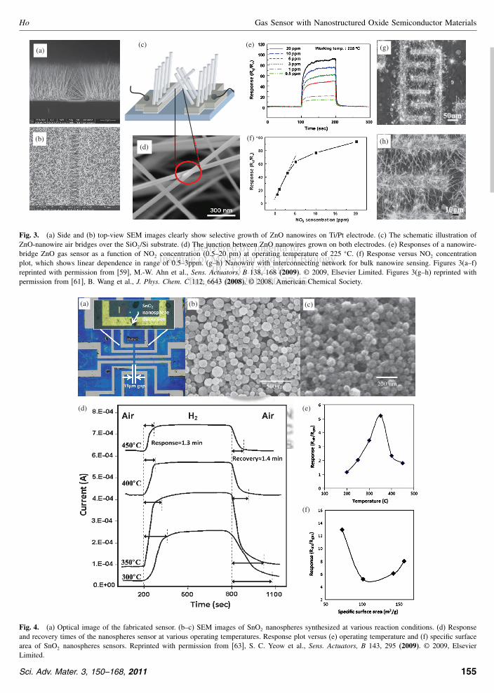
Delivered by Ingenta toInstitute of Molecular and Cell Biology
IP 13713239Tue 19 Jun 2012 003745
REVIEW
Ho Gas Sensor with Nanostructured Oxide Semiconductor Materials
(c) (e)
(f)(b)
(a)
(d)
(g)
(h)
Fig 3 (a) Side and (b) top-view SEM images clearly show selective growth of ZnO nanowires on TiPt electrode (c) The schematic illustration ofZnO-nanowire air bridges over the SiO2Si substrate (d) The junction between ZnO nanowires grown on both electrodes (e) Responses of a nanowire-bridge ZnO gas sensor as a function of NO2 concentration (05ndash20 pm) at operating temperature of 225 C (f) Response versus NO2 concentrationplot which shows linear dependence in range of 05ndash3ppm (gndashh) Nanowire with interconnecting network for bulk nanowire sensing Figures 3(andashf)reprinted with permission from [59] M-W Ahn et al Sens Actuators B 138 168 (2009) copy 2009 Elsevier Limited Figures 3(gndashh) reprinted withpermission from [61] B Wang et al J Phys Chem C 112 6643 (2008) copy 2008 American Chemical Society
(a) (b) (c)
(d)
(f)
(e)
Fig 4 (a) Optical image of the fabricated sensor (bndashc) SEM images of SnO2 nanospheres synthesized at various reaction conditions (d) Responseand recovery times of the nanospheres sensor at various operating temperatures Response plot versus (e) operating temperature and (f) specific surfacearea of SnO2 nanospheres sensors Reprinted with permission from [63] S C Yeow et al Sens Actuators B 143 295 (2009) copy 2009 ElsevierLimited
Sci Adv Mater 3 150ndash168 2011 155
Delivered by Ingenta toInstitute of Molecular and Cell Biology
IP 13713239Tue 19 Jun 2012 003745
REVIEW
Gas Sensor with Nanostructured Oxide Semiconductor Materials Ho
sensor at different operating temperatures (200ndash450 C)are shown in Figure 4(e) As such a higher operatingtemperature leads to a greater change in conductance andhence greater response On the other hand desorption ofall oxygen ionic species previously adsorbed occurs at hightemperatures which explains the reduction in response asoperating temperature is increased beyond the optimumvalue Furthermore the effect of specific surface area onthe gas sensing performance is studied Figure 4(f) showsthe response plot obtained at 350 C for all the sampleswith different specific surface areas It can be observedthat it is not a linear relationship A possible explanationis that the inner surfaces of the porous nanospheres arenot fully utilized for gas detection due to the limitation ofdiffusion of the analyte gas through the nanoporesSysoev et al have reported thin film of nanoparticles
and nanowires sensor mounted on microchip64 The devicehas demonstrated an excellent performance as a gas sen-sor capable of detecting and discriminating between sev-eral reducing gases in air at a ppb level of concentra-tion Both nanoparticles film and nanowire mats weredeposited onto thermally oxidised SiO2Si substrates withPt strip electrodes and Pt meander heaters microarray TheSnO2 nanoparticles layers were deposited onto the sub-strates by spin-coating from an aqueous colloidal disper-sion of the nanoparticles (Fig 5(a)) SnO2 nanowires aredry transferred to substrate to yield one-two monolayernetwork of percolating nanowires (Fig 5(b)) Figures 5(cndashd) depict the experimental data on a long-term evolution of
(a)
(b)
(c)
(d)
Fig 5 HRTEM and SEM images of (a) SnO2 mesoporous nanoparticles layer and (b) SnO2 nanowires (c) Response and (d) resistance of thenanoparticles (open circles) and nanowires (filled circles) over time Reprinted with permission from [64] V V Sysoeva et al Sens Actuators B139 699 (2009) copy 2009 Elsevier Limited
the SnO2 nanostructures sensing characteristics toward the2-propanol vapor The response of nanowire mat to 1 ppmof 2-propanol is about sim64 The as-prepared nanoparti-cles sensor exhibits a high response of sim4times103 How-ever over 48 days the nanoparticle response drops rapidlyto 16 close to the nanowires sensor capability It hasbeen postulated that the initial high porosity nanoparti-cles allow high gas diffusion thus rendering high responseNevertheless the long-term exposure to 2-propanol vaporsat elevated operating temperature seems to facilitate sin-tering of nanoparticles Thus the two-terminal nanowiresensor is predicted to be a better conductometric gassensor with relatively high gas sensitivity and long-termstabilityOther work on two terminal sensors is based on SnO2
nanowires which were synthesized by thermal evaporationat 900 C65 The obtained nanowires were doped with pal-ladium by coating the nanowires with palladium chloride(PdCl2 and annealed at 350 C for 30 min in air in orderto decompose PdCl2 (Figs 6(andashb)) Gas sensors based onundoped 08 wt Pd-doped and 2 wt Pd-doped SnO2
nanowires were fabricated These SnO2 nanowire gas sen-sors showed a reversible response to H2 gas at operatingtemperature of 150 C (Figs 6(cndashd)) The sensor responseincreased with Pd concentration The 2 wt Pd-dopedSnO2 nanowire sensor showed a response as high as 253for 1000 ppm H2 gas at 100
C (Fig 6(d)) Pd doping hasdemonstrated to improve the sensor response and lowerthe operating temperature
156 Sci Adv Mater 3 150ndash168 2011
Delivered by Ingenta toInstitute of Molecular and Cell Biology
IP 13713239Tue 19 Jun 2012 003745
REVIEW
Ho Gas Sensor with Nanostructured Oxide Semiconductor Materials
(c)
(d)
(a) (b)
Fig 6 (andashb) TEM image of a 2 wt Pd-doped SnO2 nanowire with adiameter of 80 nm Inset shows the diffraction pattern of PdO nanopar-ticle on the nanowire Changes in the resistance of (c) undoped and(d) 2 wt Pd-doped SnO2 nanowire gas sensors upon exposure to 100200 400 800 and 1000 ppm of H2 gas Reprinted with permissionfrom [65] Y B Shen et al Sens Actuators B 135 524 (2009) copy 2009Elsevier Limited
(e)
Fig 7 (andashb) SEM images and (cndashd) IndashV curves of the single and multiple ZnO nanowire FETs respectively (e) The typical response curves ofthe single and multiple ZnO nanowire for variations of hydrogen concentration ranging from 50 to 100 ppm at 200 C Reprinted with permissionfrom [67] R Khan et al Sens Actuators B 150 389 (2010) copy 2010 Elsevier Limited
23 FET Nanostructure Sensor
In the case of field effect transistor sensor active nanowiresensor element can act as a resistive element whose resis-tance can be changed by the field-effect or charge transferprocess66ndash69 The sensing properties can be monitored byvarying the gate potential For instance Huang et al66 havereported a highly sensitive single Ga2O3 nanowire sensorwhich operates at room temperature although it is well-known fact that the Ga2O3 films sensors usually operateat high temperature of 400 to 1000 C The room temper-ature sensitivity observed here is most likely due to thegood crystallinity and ultrahigh surface-to-volume ratiosof the one-dimensional nanostructures The gas-sensingmeasurements were performed for an individual Ga2O3
nanowire device with two AuTi electrodes and the source-drain biased voltage fixed at 10 V When the individualGa2O3 nanowire is exposed to a mixed flow of ammonia(1000 ppm) and air the current is increased dramaticallyin the first 100 seconds and enhanced to about 30 timesand stabilized at sim7800 nA The Ga2O3 nanowire deviceexhibits a sensitivity of about 38 and a response time ofsim58 s in the ambient of 1000 ppm air-diluted NH3Khan et al have reported single and multiple nanowire
FET sensors67 Figures 7(a and b) show typical SEMimages of the single and multiple ZnO nanowire FETdevices70 For comparison purposes the distance betweenthe electrodes and the diameter of the ZnO nanowires werekept the same for both devices Figures 7(c and d) exhib-ited the typical electrical characteristics for the n-type sin-gle and multiple ZnO nanowire FETs respectively Themultiple nanowire devices showed greatly enhanced con-ductance due to increased number of nanowire Figure 7(e)shows the gas sensing characteristics as a function of timefor the single and multiple ZnO nanowires with varioushydrogen concentrations in the range of 50ndash100 ppm at200 C The sensor response was higher for the multiple
Sci Adv Mater 3 150ndash168 2011 157
Delivered by Ingenta toInstitute of Molecular and Cell Biology
IP 13713239Tue 19 Jun 2012 003745
REVIEW
Gas Sensor with Nanostructured Oxide Semiconductor Materials Ho
(a)
(b)
(c)
(d)
Fig 8 IndashVg curves before and after exposure to (a) 100-ppm NO2 and (b) 1 NH3 The response time of (c) 20 2 and 05 ppm NO2 and (d) 002NH3 Reprinted with permission from [68] C Li et al Appl Phys Lett 82 1613 (2003) copy 2003 American Institute of Physics
(a)
(b)
(c)
(d)
Fig 9 Schematic of (a) single and (b) multiple nanowire transistor structure where TiAu are deposited on nanowire-decorated SiSiO2 substrateas drain and source electrodes (c) IndashVg and (d) GGo versus time for the single and multi nanowire sensor device recorded at different NO2
concentrations Reprinted with permission from [72] D H Zhang et al Nano Lett 4 1919 (2004) copy 2004 American Chemical Society
158 Sci Adv Mater 3 150ndash168 2011
Delivered by Ingenta toInstitute of Molecular and Cell Biology
IP 13713239Tue 19 Jun 2012 003745
REVIEW
Ho Gas Sensor with Nanostructured Oxide Semiconductor Materials
ZnO nanowires than the response for the single ZnOnanowire over the entire range of hydrogen concentra-tion The multiple nanowires FET are made up of nano-junctions which acted as a potential barrier for electronflow The potential barrier decreased as the nanowire wasexposed to the reducing gas resulting in an increase inthe current flow The potential barrier modulation of mul-tiple nanowires was more efficient than the modulation ofthe surface depletion of the single ZnO nanowire in gassensing Therefore the potential barrier modulation in thenanojunctions caused the enhanced sensor response for themultiple nanowiresLi et al68 demonstrated the use of a single one-
dimensional nanowire FET sensor for high performanceroom temperature sensing The sensor is made up ofIn2O3 nanowires of diameter 10 nm and length 5 mwhich were placed between the source and drain elec-trodes with a silicon substrate as a back gate (Fig 8 inset)The as-fabricated In2O3 nanowire sensor devices exhib-ited typical n-type transistor characteristics The individualIn2O3 nanowire transistors sensors exhibited superior per-formance as such the sensitivity is of 106 for NO2 and 105
for NH3 which are four or five orders of magnitude betterthan results obtained from the thin-film based sensors71
Response times are as short as 5 s for 100-ppm NO2 and10 s for 1 NH3 The lowest detectable gas concentrationsare 05 ppm for NO2 and 002 for NH3
Furthermore the sensing and selectivity between dif-ferent gases can be studied by monitoring the currentdependence on the gate bias and the threshold voltageshift rendering a significant advantage over thin-film-based devices Figure 8(a) shows two currentndashgate volt-age (IndashVg) curves measured before and after exposure to100 ppm NO2 in argon with a constant source drain volt-age (Vds of minus03 V Both measurements suggest that theIn2O3 nanowires are n-type semiconductor as the con-ductance increase with gate bias There is also a pro-nounced shift in the threshold voltage from minus48 V before
(c)
Fig 10 (a) TEM of nanowires and nanobelts (b) Schematic view of device used for the in situ conductometric measurements under gas exposure andmetal deposition (c) Response of a pristine (dashed line) and Pd-functionalized (solid line) nanostructure to sequential oxygen and hydrogen pulses at473 K (top pane) and 543 K (bottom) Reprinted with permission from [73] A Kolmakov et al Nano Nano Lett 5 667 (2005) copy 2005 AmericanChemical Society
the exposure to 20 V after the exposure Adsorption ofoxidizing gases reduces the number of free electrons inthe n-type semiconductor and thus reduces the conductiv-ity Figure 8(b) shows two IndashVg curves before and afterexposing to diluted NH3 in Ar with Vds =minus03 V A largethreshold voltage shift from 248 V to 216 V is observedwith a maximum sensitivity of 105 at Vg = minus30 V ForNO2 concentrations of 20 2 and 05 ppm the responsetimes are determined to be 20 s 5 min and 10ndash12 minrespectively (Fig 8(c)) Figure 8(d) shows a response timeof about 2 min for 002 NH3 which is the lowest testedconcentration The limitation is imposed by the availabilityof highly diluted NH3 in air or argonZhang et al72 have demonstrated FET NO2 sensor down
to ppb levels based on both single and multiple In2O3
nanowires operating at room temperature as shown inschematic diagram Figures 9(a and b) Figure 9(c) showsthe conductance versus gate bias (Vg curves recorded inthe six different NO2 concentrations after exposure for20 min for single nanowire FET The threshold gate volt-age shifted rightward monotonically with the increasingNO2air concentration implying the gradual suppressionof carrier concentration of nanowire that scales linearlywith the absolute value of gate threshold As for the multinanowire FET the typical number of nanowires bridg-ing adjacent metal electrodes is estimated to be 100ndash200Figure 9(d) shows the sensing cycles of the multiwire FETdevice corresponding to NO2air concentrations of 5 1020 50 100 and 200 ppb The multiwire sensor showeda lower detection limit of 5 ppb compared to the 20 ppblimit of single nanowire sensors The room temperaturedetection limit is one of the lowest level ever reportedFurthermore selective detection of NH3 O2 CO and H2
is possible with this nanowire FET sensorKolmakov et al has demonstrated an enhanced 1-D
SnO2 nanostructure-based sensor with and without Pdnanoparticles decorated nanobelts (Fig 10(a))73 Thedeposited Pd works as catalysts for oxygen dissociation
Sci Adv Mater 3 150ndash168 2011 159
Delivered by Ingenta toInstitute of Molecular and Cell Biology
IP 13713239Tue 19 Jun 2012 003745
REVIEW
Gas Sensor with Nanostructured Oxide Semiconductor Materials Ho
Figure 10(b) shows the schematic view of device used forthe in situ conductometric FET measurements under gasexposure and metal deposition The sensing performanceof a SnO2 nanowire toward sequential oxygen and hydro-gen pulses at two different temperatures before (dashedcurves) and after (solid curves) Pd deposition is shownin Figure 10(c) Functionalizing the nanowire surface withPd leads to an enhancement in IDS response for both gasesand shorter response time Functionalizing the nanowiresurface with Pd leads to an enhancement in IDS responsefor both gases and to an increased speed of response Pdmetal nanoparticles grown on reduced n-SnO2 nanowiresand nanobelts were found to form Schottky-barrier likejunctions which locally deplete the nanostructure of elec-trons The improvements of sensitivity can be explained bythe combined ldquospillover effectrdquo of atomic oxygen formedcatalytically on the Pd particles then migrating onto thetin oxide and the back spillover effect in which weaklybound molecular oxygen migrate to the Pd and are cat-alytically dissociated Raising the temperature raises thevalue of IDS and shortens the response time of the sensorto O2 and H2 This effect is most prominent for oxygenfor which the nanostructure only becomes activated above543 K
3 DIRECTED ASSEMBLY OFNANOSTRUCTURE SENSORS
The application of nanostructures as building blocks forsensor can be achieved by implementing effective assem-bly and integration techniques to transfer the nanostructuresfrom growth substrates onto their respective device sub-strates Several methods have been developed to assembleone-dimensional nanostructures which include microflu-idic channel Langmuir-Blodgett blown bubble film self-assembled monolayers transfer printing alignment etcIn essence these approaches employ external forces toalign the nanostructures via wet or dry media In someapproaches multilayer alignment is possible while oth-ers allow selective spatial alignment in large-scale Thedevelopment of nanostructures based sensor generallyinvolves two processes First the assembly of nano-structures into highly integrated arrays with controlledorientation and spatial position second integration of inter-connects between nanostructures and the micro or macro-scopic subsystems
31 Transfer Printed Nanostructure Sensor
Transfer printing is a dry alignment technique wherebynanostructures are printed in contact or close proximityto the substrate allowing the nanostructures to be alignedin the same direction and in a predetermined densityThe nanostructures are grown on a substrate ldquostampsrdquoand then stamped ldquoprintedrdquo onto the receiving substrate
The receiving substrate can have pre deposited electrodesupon which nanostructures can be aligned The transferprinting deposition strategy has demonstrated to lead towell-defined and reproducible three-dimensional integratedcircuits structures of controlled nanowiresrsquo density andalignment over large substrate areas7475
Layer-by-layer assembly of nanowires for three-dimensional multifunctional electronics has been reportedby Javey et al74 The dry alignment process involves(i) optimized growth of designed nanowires by nanoclus-ter directed synthesis and(ii) patterned transfer of nanowires directly from ananowire growth substrate to a second device substrate viacontact printing (Figs 11(andashb))
In detail a photolithographically patterned device sub-strate is first firmly attached to a bench top and thenanowire growth substrate is placed face down in con-tact with the patterned device substrate A gentle man-ual pressure is then applied from the top followed bysliding the growth substrate by 1ndash3 mm before thegrowth substrate is removed Devices and circuits arethen fabricated on the printed arrays of nanowires usingconventional top-down lithography and metallization pro-cesses To fabricate a three-dimensional FET the con-tact printing of nanowires and device fabrication stepsare repeated several times along with the deposition ofSiO2 insulating layer in order to obtain vertically stackedelectronic layers (Figs 11(cndashd)) Another work which isalso reported by the same group is ordered arrays ofsingle-crystalline nano- and microwires of GaAs and InPwith well-controlled lengths widths and shape have beenfabricated over large areas from high quality bulk wafersby the use of traditional photolithography and anisotropicchemical wet etching75 Printing using elastomeric stampscan transfer these wire arrays to plastic substrates withexcellent retention of order and crystallographic orienta-tion of the wires Figure 11(e) shows the various printingconfiguration single to triple layers of nanowires patternsElectrical measurements on simple test structures demon-strate the high degree of mechanical flexibility of theresulting wire arrays on plastics The combination of topdown wire fabrication and transfer printing represents aneffective route to ultrahigh performance macroelectronicsystemsThe nanowires are observed to be cleanly printed
only at lithographically predefined locations FET device(Figs 14(cndashd)) The printed nanowires are aligned uni-formly across mm or larger scale with relatively highdensities (sim4 nanowirem) The monolithic integration ofindividual and parallel arrays of multifunctional and multi-layer circuits consists of up to 10 addressable vertical lay-ers This alignment methodology is applicable for the widerange of nanowire materials substrates and device designsFurthermore the simplicity and the low processing tem-perature requirement of the method makes it ideal for
160 Sci Adv Mater 3 150ndash168 2011
Delivered by Ingenta toInstitute of Molecular and Cell Biology
IP 13713239Tue 19 Jun 2012 003745
REVIEW
Ho Gas Sensor with Nanostructured Oxide Semiconductor Materials
(e)
Fig 11 Overview of 3D nanowire circuit integration (a) Contact printing of nanowire from growth substrate to prepatterned substrate (b) 3Dnanowire circuit is fabricated by the iteration of the contact printing device fabrication and separation layer deposition steps (c) Optical microscopeimage of 3D nanowire FETs (d) Dark field image shows a parallel array of nanowires aligned between source (S) drain (D) and top gate (G)electrodes Reprinted with permission from [74] A Javey et al Nano Lett 7 773 (2007) copy 2007 American Chemical Society (e) Images of singleto multiple layers of GaAs wire array which are transfer printed using elastomeric stamps Reprinted with permission from [75] Y G Sun and J ARogers Nano Lett 4 1953 (2004) copy 2004 American Chemical Society
achieving high performance three-dimensional integratedcircuitry with different functionalities in distinct layersTo demonstrate the potential of nanowire printing for
large-area sensor integration printed Si-nanowire arrayswere configured as H2 sensors P -type SiNWs were printedon Si substrates and two-terminal devices with Ni sili-cide contacts were fabricated77 The conductance of theSi nanowire array shows a strong dependence on the H2
exposure even at relatively low concentrations (250 ppm)It is worth noting that the nanowire printing method mayprovide a viable route toward the realization of electronicnoses and smart sensors capable of distinguishing chem-ical species while determining their concentrations Suchsensors may be envisioned through a large-scale integra-tion of different sensor components interfaced with signal-processing functions To achieve this goal heterogeneousassembly of nanowire materials with orthogonal sensitivityto different analytes is needed which may be achievedthrough a multistep nanowire printing process
32 Dielectrophoretic AssembledNanostructure Sensor
Dielectrophoresis (DEP) technique utilizes the dielectro-phoretic force acting on the particles to induce spatial
movement when exposed to a non uniform electric field inthe suspension medium The force depends on a numberof parameters such as the arrangement of the electrodethe frequency of the electric field and the resulting elec-tric field distribution as well as the dielectric propertiesof the particles and the surrounding medium By changingthese factors this force will pull the particle towards thehigher electric field region (positive DEP effect) or push ittowards the lower field region (negative DEP effect) DEPis a manipulation technique based on Maxwellrsquos classicalelectromagnetic field theory to allow controlled movementof particles in a controlled electric field between the presetelectrode structures The DEP technique has demonstratedthe potential for the construction of the nanosensors ornanoelectronic devices using as the nanostructured mate-rial as the building blocksJiang et al78 have reported work on manipulation of ZnO
nanorods by applying AC signals of suitable frequency andvoltage to provide non uniform electrical field on differentpatterns of electrode (Figs 12(andashb)) Similarly Li et al79
have proposed DEP assembly of nanowires onto interdigi-tated microelectrodes (Fig 12(c)) and mounted on micro-hotplate sensor platform (Fig 12(d))Template-assisted electrodeposition method and a
two-step thermal oxidation are employed Through
Sci Adv Mater 3 150ndash168 2011 161
Delivered by Ingenta toInstitute of Molecular and Cell Biology
IP 13713239Tue 19 Jun 2012 003745
REVIEW
Gas Sensor with Nanostructured Oxide Semiconductor Materials Ho
(a)
(b) (d)
(c)
Fig 12 (andashb) Low and high resolution SEM images of aligned ZnO nanowire in the interdigitated electrode array The voltage and the frequency ofthe applied electric field are 10 V and 5 kHz Reprinted with permission from [78] K W Jiang et al Sens Actuators B 134 79 (2008) copy 2008Elsevier Limited (c) Well dispersed and fairly aligned indiumtin nanowires bridged across the electrode array (d) Overview of the integrated sensorchip on micro-hotplate Reprinted with permission from [79] X P Li et al Sens Actuators B 148 404 (2010) copy 2008 Elsevier Limited
DEP(Sine waves)
Thermal andoxidationtreatment
Gas sensingmeasurement
Prefabrication of electrodes
Nanowire dispersion
Fig 13 Schematic of nanowire sensor integration nanowire suspension drop casting on interdigitated microelectrodes DEP assembly of metalnanowires alignment of nanowires on microelectrodes two-step thermal oxidation of nanowires and final integrated sensor chip The response curve ofthe various volatile organic compounds versus temperature Reprinted with permission from [80] T Jinkawa et al J Mol Catal A 155 193 (2000)copy 2008 Elsevier Limited
162 Sci Adv Mater 3 150ndash168 2011
Delivered by Ingenta toInstitute of Molecular and Cell Biology
IP 13713239Tue 19 Jun 2012 003745
REVIEW
Ho Gas Sensor with Nanostructured Oxide Semiconductor Materials
electrodeposition synthesis method one-dimensionalindium oxide tin oxide and indiumndashtin oxide nanowireswere successfully fabricated The nanowires are uniformand easy to process and assemble with good control ofchemical compositions The process flow of fabricatingnanowire sensor via DEP alignment process is shown inFigure 1380 The nanowires solution is prepared and dropcasted onto prefabricated interdigitated electrodes Thenanowires are observed to be randomly dispersed on theelectrodes The electrical field was generated by connect-ing a function generator to the interdigitated electrodeswhile a sinusoidal wave with a frequency of 5ndash6 MHzand peak-to-peak voltage of 6 V was applied during theDEP process At room temperature ethanol volatizedwithin minutes leaving nanowires aligned between theelectrode pairs Two thermal treatment processes werecarried out after the DEP assembly of nanowires to lowerthe contact resistance between the aligned nanowires andmicroelectrodes and increased the stability of the nanowireassembled First aligned metal nanowires were heated toabout 10 C below their melting points the temperaturevaried according to different material compositions Thebonding process was carried out in an inert nitrogenenvironment to prevent oxidation Next nanowires wereheated at the temperature just below the melting point ofthe respective material in an atmospheric environment for2 h The temperature was later raised to 400ndash500 C foranother 3 h to achieve full oxidation After the thermaland oxidation treatment the nanowire sensor chip wasready for electrical measurement and chemical response
ndash500
ndash400
ndash300
ndash200
ndash100
00
100
18E+10
22E+10
26E+10
30E+10
34E+10
38E+10
42E+10
0 600 1200 1800 2400 3000 3600 4200 4800
2500ppmH2
2000ppmH2
1154ppmH2
1000ppmH2
CDA CDA CDACDA
ndash350
ndash300
ndash250
ndash200
ndash150
ndash100
ndash50
00
50
100
40E+09
45E+09
50E+09
55E+09
60E+09
65E+09
70E+09
0 300 600 900 1200 1500 1800 2100 2400 2700
Time (s)
Time (s)
Res
ista
nce
(Ω)
Res
ista
nce
(Ω)
Sen
sitiv
ity (
)
Sen
sitiv
ity (
)
UV onUV on
UV off UV off
(a)
(c) (d)
(b)(e)
(f)
Fig 14 SEM images of (a) cotton textile substrate in low magnification (b) bare cotton fibres (c) ZnO nanorods-coated cotton fibres and (d) highmagnification images of ZnO nanorods on a cotton fibre Scale bar in the inset represents 100 nm Electrical responses of ZnO nanorods-on-cloth deviceto (e) various concentrations of H2 gas and (f) UV irradiation Clean dry air (CDA) was used to flush the chamber before and after each hydrogeninjection Experiments were performed in room temperature Reprinted with permission from [89] Z H Lim et al Sens Actuators B 151 121 (2010)copy 2010 Elsevier Limited
testing The sensor was investigated with different volatileorganic compounds The sensitivity of three alcohols isthe highest for methanol follow by ethanol isopropanolThese findings coincide with the number of methyl groupsin their chemical structure Two competitive dissociativereactions were proposed80 to explain the alcohol moleculesadsorbed on the oxide surface simply described as OndashHand CndashO bond-breaking processes where the former onehas a greater contribution to the resistance drop Thesensitivity order may relate to the preference of eachchemical over these two competitive reactions
4 NON-CONVENTIONAL SUBSTRATESENSOR
Technological and industrial difficulties in further minia-turization of devices have called for innovative ways toincorporate gadgets into articles of everyday life Thereare many sensors which have been fabricated on non con-ventional substrates namely the plastic textile and papersubstrate sensor The ability to fabricate sensor deviceson plastic substrates is important owing to the demandsof handheld portable consumer electronics Plastic sub-strates possess many attractive properties including bio-compatibility flexibility light weight shock resistancesoftness and transparency However plastics has low melt-ing point and they tend to deform or melt at tempera-tures of sim200 C This limits the synthesis temperatureof nanostructures directly on the plastic substrate Vari-ous ways to transfer the nanowires from donor substrate
Sci Adv Mater 3 150ndash168 2011 163
Delivered by Ingenta toInstitute of Molecular and Cell Biology
IP 13713239Tue 19 Jun 2012 003745
REVIEW
Gas Sensor with Nanostructured Oxide Semiconductor Materials Ho
to plastic substrate such as nanoimprint contact transferLangmuir Blogett etc have been developed In additionlow temperature synthesis processes have also been devel-oped to overcome this limitation Mc Alpine et al havereported plastic nanowire sensors based on Si nanowireswhich exhibit parts-per-billion sensitivity to NO2 a haz-ardous pollutant81
Another type of non conventional substrate sensor istextile Clothing is not only a necessity it also encom-passes a complete industry ranging from the down-to-earthbasics to the upmarket and chic Smart clothingtextiles arebecoming very popular in the past decade Smart textileswhich have been developed include silicon flexible skins
(b)
(a)
(d)
(c)
Source-meter
0
2E+09
4E+09
6E+09
8E+09
1E+10
12E+10
14E+10
16E+10
18E+10
I-V 1 I-V 2 I-V 3 I-V 4 I-V 5 Average
Res
ista
nce
(Ω)
Before After
(e)
(f)
(g)
Fig 15 SEM images of (a) low resolution ZnO-nanorods-coated textile with selected area (circled in red) for subsequent studies (b) the selected ZnOnanorods-coated yarns before stretching twisting and sonication (c) the same yarns after repeated stretching and twisting and (d) 5 minutes of watersonification (e) Schematic diagram of the electro-mechanical testing and (f) electrical properties before and after each stretching and twisting cycle(g) Electrical measurement of ZnO nanorods-on-cloth device while subjected to controlled stress cycles with a mechanical testing system Reprintedwith permission from [89] Z H Lim et al Sens Actuators B 151 121 (2010) copy 2010 Elsevier Limited
and organic transistors on textile fibers8283 Another type ofthe smart sensing textiles which uses piezo-resistive prop-erties has been developed The approach for fabricating thefabrics was to coat a thin layer of piezo-resistive materialssuch as polypyrrole or a mixture of rubbers and carbonson conventional fabrics to form fabric-based sensors84ndash86
The function of the developed sensors is similar to that offlexible strain gauges which can measure strains when theyare subjected to a tensile stress Other innovations whichare not actively explored are textiles which can detectenvironmental conditions which then react and adapt toenvironmental changes Furthermore smart textiles can bemade to measure and monitor the physiological conditions
164 Sci Adv Mater 3 150ndash168 2011
Delivered by Ingenta toInstitute of Molecular and Cell Biology
IP 13713239Tue 19 Jun 2012 003745
REVIEW
Ho Gas Sensor with Nanostructured Oxide Semiconductor Materials
of the wearer eg perspiration heartbeat etc Thus they canbe applied various healthcare systems
41 Textile Sensor
While the development of wearable devices has beenreported the incorporation of nano-materials into thedesigns has not been well explored In addition problemssuch as complex process mass production washabilityand wearing comforts needs to be well addressed The easeof synthesizing ZnO nanowires or nanorods on almost anysubstrates welcomes large-scale incorporation on textileZnO nano-structures are believed to be non-toxic and bio-safe87 allowing their direct usage in daily applicationsWhile the use of nano-materials in daily human activitiesraised questions on its potential health risks there is todate no in vivo evidence of toxicity of nano-particulateZnO88
29 nm
5 nm
1 μm1 μm
2 nm 5 μm
15Endash03
16Endash03
17Endash03
18Endash03
Time (s)
on off
1000 ppm
(a)
(c) (d)(f)
(b) (e)
15Endash03
16Endash03
16Endash03
17Endash03
17Endash03
18Endash03
18Endash03
150 250 350 450 550 650 0 150 300 450 600 750 900
Time (s)
Cur
rent
(m
A)
Cur
rent
(m
A)
on off
2000 ppm1500 ppm
1000 ppm2500 ppm
(g) (h)
Fig 16 (andashb) Low and (cndashd) high resolution TEM images of the nanobelts (e) Image of nanobelts sheet made without any addition of binder orreinforcement chemicals (f) Cross-sectional SEM image of the nanobelts sheet Current response of the sensor at (g) varying and (h) same ppm H2
concentration Reprinted with permission from [90] S Bela et al J Phys D Appl Phys 43 35401 (2010) copy 2010 Institute of Physics
SEM images of the textile and nanorods displayed inFigures 14(andashd) show radially oriented nanorods (diametersim80 nm) with hexagonal cross-section grown along thecylindrical fibres (diameter sim15 m)89 Length of thenanorods is sim1 m The nanorods form a uniform anddense coverage around entire lengths of the fibres to forma cross-linked semi-conductive textileThe conductive textile shows excellent multiple sens-
ing (gas and optical) performances at room temperature asshown in Figures 14(e) and (f) respectively In the presenceof hydrogen gas chemisorbed oxygen ions are reducedto release electrons to the conduction band of the ZnOsurface resulting in an increase in conductivity In addi-tion the reduction reaction decreases the surface densityof the oxygen adsorbate leading to a reduction in thewidth of the depletion region and the height of the sur-face potential barrier thus resulting in the decrease in theresistance of the sensor The mechanism for UV sensing
Sci Adv Mater 3 150ndash168 2011 165
Delivered by Ingenta toInstitute of Molecular and Cell Biology
IP 13713239Tue 19 Jun 2012 003745
REVIEW
Gas Sensor with Nanostructured Oxide Semiconductor Materials Ho
is similar to that of hydrogen sensing with holes fromthe photo-generated electronndashhole pairs playing the role ofremoving the adsorbed oxygen molecules insteadA notable feature of the ZnO nanorods-coated textile
device is its fine morphological and electrical stabilityunder multiple stress and washing cycles A critical chal-lenge of semi-conductive yarns and textile is its durabil-ity and constancy of electrical performance SEM analyses(Figs 15(andashd)) of the nanorods -on-cloth before and afterstretching twisting and ashing cycles show no cracks ordelamination of the nanorods from the fibres respectivelyFigure 15(e) shows a schematic of the electro-mechanicaltesting Electrical characterisations made before and aftereach stretching and twisting cycle (Fig 15(f)) show goodelectrical stability We further perform electrical conduc-tivity measurements while stretching and relaxing the tex-tile device in a controlled manner The semiconductingtextile exhibits a higher conductivity when stretched dueto tighter packing (increased contact junctions) of the ZnOnanorods-coated fibers Figure 15(g) shows the variation ofcurrent through the textile device as it underwent repeatedcycles of stress and relaxation When the stress is releasedconductivity falls and stabilises to the original state Againthe morphology of the nanorods-on-textile suffered nocracks of delamination or noticeable degradation after theelectromechanical testing
42 Free Standing Sheet Sensor
Another non conventional sensor substrate is a free stand-ing sheet of nanowire paper The nanostructures are tobe produced in gram quantities so that it can be easilymade into nanostructured paper sheet The thickness ofthe nanostructures sheet can be tuned according to theamount of nanostructures used After the filtering wascompleted a sheet of nanostructures was formed by sand-wiching between a metal calender which was pressed andheated to ensure the nanowires are well dried and bondedtogether to form the free-standing paperBela et al have been reported synthesis of hybrid
titanate and titania nanobelts (Figs 16(andashd)) in a large-scale quantity for gas sensing applications90 The nanobeltsare synthesized from TiO2 powder based on hydrolysis andion exchange of NaOH base and HCl acid respectivelySheets of as-synthesized nanobelts are used for electricaland gas sensing measurements Figure 16(e) shows thewhite nanobelts sheet made without any addition of binderor reinforcement chemicals Cross-sectional SEM image ofFigure 16(f) shows that the nanobelts sheet has a thicknessof sim15 m Figures 16(g and h) show the current responseof the sensor at varying and same ppm H2 concentra-tions respectively The measurements were conducted at anoperating temperature of 300 C From the graphs it is evi-dent that the introduction of hydrogen causes the resistanceof the sensor to reduce because of the injection of electrons
onto the surface of the metal-oxide nanostructures therebyimproving the conductivity of the bulk sensing capabili-ties The resistance increases as the concentration of H2 isvaried from 2500 to 1000 ppm The response time (90of Rair minusRgas is achieved within the first 40ndash50 s whilethe recovery time is 10ndash12 min From the Figure 7(c) itwas observed that the sensing response was rather stableand reversible In oxidizing atmosphere of 300 C ambi-ent oxygen is adsorbed on the surface of nanobelts mostlikely with a negative charge Subsequently with the intro-duction of a reducing H2 gas it reacts with the negativelycharged surface oxygen and decreases the resistance bythe injection of electron
5 CONCLUSIONS
There is an immense technological and scientific potentialsof nanostructured materials in nanodevice applicationsand already numerous nanomaterial based sensors usingvarious materials have been reported These oxide materi-als can be synthesized by various synthetic routes whichinclude both physical and chemical methods The poten-tial application of these nanostructures as sensor dependsgreatly on the ability to precisely control their dimensionchemical composition surface property phase purity andcrystal structure Sensor of various configurations bulktwo-terminal and FET device have been fabricated Theintegrability of the nanostructure sensor into microelec-tronic fabrication technology is an issue that needs tobe addressed Various ways to assemble nanowires so asto ease the device fabrication process have been devel-oped The recent advances in assembling larger and morecomplex nanowire sensor arrays and integrating them intonanoscale electronics can lead to exquisite sensor sys-tem performances These sensory systems can sensitivelytransduce gaschemicalbiological binding events into elec-tronicdigital signals which promise a sophisticated nano-electronics sensing system
6 FUTURE DIRECTIONS
Although nanomaterial based sensors are expected to out-perform their bulk component there are still many issuesand parameters to be studied and addressed Parameters tobe explored include structural and composition tuning aswell as doping and functionalization of surfaces to increaseselectivity sensitivity and materials integrity for long-termstability Other parameters such as limits of detection lim-its of quantification dynamic range response and recov-ery times and lifetime have to be studied and improvedas well The long-term reliability of a sensor is impor-tant since progressive drifts in the characteristics andorresponses of the sensors affect accurate testing and analy-sis The drift of the sensors are frequently related to highworking temperatures and exposure to chemically active
166 Sci Adv Mater 3 150ndash168 2011
Delivered by Ingenta toInstitute of Molecular and Cell Biology
IP 13713239Tue 19 Jun 2012 003745
REVIEW
Ho Gas Sensor with Nanostructured Oxide Semiconductor Materials
ambient gas Many other issues include aging grain-sizegrowth poisoning due to unknown chemical species dif-fusion processes within the device etc are to be addressedas wellThe future direction of the solid-state gas sensor is
towards integrated wirelessremote multi-purpose sens-ing high selectivity recognition of a specific biological orchemical species with ldquoelectronic-nose-tonguerdquo capabili-ties In addition development of miniaturized analyticalsensor which can be integrated in-line orand as standaloneportable sensors is paramount for industrial applicationsThe sensors can further be refined into a network of sensorarrays providing rapid screening monitoring and reportingsystem The data are collected in a database and form partof a feedback guidance system to the control algorithm inindustrial processes
Acknowledgments The work is supported by NationalUniversity of Singapore grant R-263-000-532-112Images used for the cover page are kindly contributed byZ H Lee and M Kevin multidisciplinary laboratory
References and Notes
1 D James S M Scott Z Ali and W T OrsquoHare Microchim Acta149 1 (2005)
2 C-D Kohlin Nanoelectronics and Information Technology editedby R Waser Wiley-VCH Berlin (2005) p 851
3 M E Franke T J Koplin and U Simon Small 2 36 (2006)4 A Kolmakov and M Moskovits Annu Rev Mater Res 34 151
(2004)5 A Mandelis and C Christofides Physics Chemistry and Technology
of Solid State Gas Sensor Devices Wiley-Interscience New York(1993)
6 P T Moseley Sens Actuators B 6 149 (1992)7 N M White and J D Turner Meas Sci Technol 8 1 (1997)8 D Kohl J Phys D 34 R125 (2001)9 N Pinna G Neri M Antonietti and M Niederberger Angew
Chem Int Ed 43 4345 (2004)10 L P Sun L H Huo H Zhao S Gao and J G Zhao Sens Actu-
ators B 114 387 (2006)11 Z F Liu T Yamazaki Y B Shen T Kikuta N Nakatani and
Y X Li Sens Actuators B 129 666 (2008)12 C S Rout A R Raju A Govindaraj and C N R Rao J Nanosci
Nanotechnol 7 1923 (2007)13 M S Arnold P Avouris Z W Pan and Z L Wang J Phys
Chem B 107 659 (2003)14 I Jimenez I M A Centeno R Scotti F Morazzoni A Cornet
and J R Morante J electrochem Soc 150 H72 (2003)15 S Semancik and R E Cavicchi Thin Solid Films 206 81 (1991)16 N S Baik G Sakai N Miura and N Yamazoe Sens Actuators B
63 74 (2000)17 M Ivanovskaya P Bogdanov G Faglia and G Sberveglieri Sens
Actuators B 68 344 (2000)18 K Ihokura and I Watson The Stannic Oxide Gas Sensormdash
Principles and Applications CRC Press Boa Raton (1994)19 K D Schierbaum U Weimar and W Gopel Sens Actuators B
7 1 (1992)20 G Korotcenkov Sens Actuators B 121 664 (2007)21 J G Lu P C Chang and Z Y Fan Mater Sci Eng 52 49 (2006)22 T Yamamoto and H Katayama-Yoshida Jpn J Appl Phys
38 L166 (1999)
23 J G Lu L P Zhu Z Z Ye F Zhuge B H Zhao D W MaL Wang and J Y Huang J Mater Sci 41 467 (2006)
24 J Zhong S Muthukumar Y Chen Y Lu H M Ng W Jiang andE L Garfunkel Appl Phys Lett 83 3401 (2003)
25 S Y Bae C W Na J H Kang and J Park J Phys Chem B109 2526 (2005)
26 S Y Li P Lin C Y Lee T Y Tseng and C J Huang J Phys DAppl Phys 37 2274 (2004)
27 D K Hwang H S Kim J H Lim J Y Oh J H Yang S J ParkK K Kim D C Look and Y S Park Appl Phys Lett 86 151917(2005)
28 W Lee M C Jeong S W Joo and J M Myoung Nanotechnology16 764 (2005)
29 W Lee M C Jeong and J M Myoung Appl Phys Lett 85 6167(2004)
30 D W Zeng C S Xie B L Zhu R Jiang X Chen W L SongJ B Wang and J Shi J Cryst Growth 266 511 (2004)
31 G Z Shen J H Cho J K Yoo G C Yi and C J Lee J PhysChem B 109 5491 (2005)
32 J B Cui and U J Gibson Appl Phys Lett 87 133108 (2005)33 C X Xu X W Sun Z L Dong M B Yu Y Z Xiong and J S
Chen Appl Phys Lett 86 173110 (2005)34 D A Schwartz K R Kittilstved and D R Gamelin Appl Phys
Lett 85 1395 (2004)35 C Ronning P X Gao Y Ding Z L Wang and D Schwen Appl
Phys Lett 84 783 (2004)36 A J Mieszawska R Jalilian G U Sumanasekera and F P
Zamborini Small 3 722 (2007)37 B Zhu K Li S Zhang S Wu and W Huang Prog Chem 20 48
(2008)38 J X Wang S S Xie and W Zhou MRS Bull 32 123 (2007)39 W Lu and C M Lieber J Phys D-Appl Phys 39 R387
(2006)40 X Wang and Y D Li Inorganic Chemistry 45 7522 (2006)41 Y Shen T Yamazaki Z Liu D Meng T Kikuta N Nakatani
M Saito and M Mori Sens Actuators B 135 524 (2009)42 A Kolmakov Y Zhang G Cheng and M Moskovits Adv Mater
15 997 (2003)43 X T Zhou J Q Hu C P Li D D D Ma C S Lee and S T
Lee Chem Phys Lett 369 220 (2003)44 T-J Hsueh C-L Hsu S-J Chang and I-C Chen Sens Actua-
tors B 126 473 (2007)45 Q Wan Q H Li Y J Chen T H Wang X L He J P Li and
C L Lin Appl Phys Lett 84 3654 (2004)46 G J Li X H Zhang and S Kawi Sens Actuators B 60 64 (1999)47 G J Li and S Kawi Talanta 45 759 (1998)48 E T H Tan G W Ho A S W Wong S Kawi and A T S Wee
Nanotechnology 19 255706 (2008)49 S Luo G Fu H Chen and Y Zhang Mater Chem Phys 109 541
(2008)50 C Y Wang M Ali T Kups C C Roehlig V Cimalla T Stauden
and O Ambacher Sens Actuators B 130 589 (2008)51 J Ahmed S Vaidya T Ahmad P Sujatha Devi D Das and A K
Ashok Mater Res Bull 43 264 (2008)52 J Kaur R Kumar and M C Bhatnagar Sens Actuators B
126 478 (2007)53 D Lutic M Strand A Lloyd-Spetz K Buchholt E Ieva P O
Kall and M Sanati Top Cata 45 105 (2007)54 A Teleki S E Pratsinis K Kalyanasundaram and P I Gouma
Sens Actuators B 119 683 (2006)55 X L Gou G X Wang X Y Kong D Wexler J Horvat J Yang
and J Park Chem Eur J 14 5996 (2008)56 X Feng Z J Li P Y Wang and Y F Zhou J Mat Sci 40 6597
(2005)57 J Chen L Xu W Li and X Gou Adv Mater 17 582 (2005)58 Z B Zhuang Q Peng J F Liu X Wang and Y D Li Inorg
Chem 46 5179 (2007)
Sci Adv Mater 3 150ndash168 2011 167
Delivered by Ingenta toInstitute of Molecular and Cell Biology
IP 13713239Tue 19 Jun 2012 003745
REVIEW
Gas Sensor with Nanostructured Oxide Semiconductor Materials Ho
59 M-W Ahn K-S Park J-H Heo D-W Kim K J Choi and J-GPark Sens Actuators B 138 168 (2009)
60 H T Wang B S Kang F Ren L C Tien P W Sadik D PNorton S J Pearton and J Lin Appl Phys A 81 1117 (2005)
61 B Wang L F Zhu Y H Yang N S Xu and G W Yang J PhysChem C 112 6643 (2008)
62 T H Jung S-I Kwon J-H Park D-G Lim Y-J Choi and J-GPark Appl Phys A 91 707 (2008)
63 S C Yeow W L Ong A S W Wong and G W Ho Sens Actu-ators B 143 295 (2009)
64 V V Sysoeva T Schneiderb J Goschnickb I KiselevbW Habichtb H Hahnb E Strelcovc and A Kolmakov Sens Actu-ators B 139 699 (2009)
65 Y B Shen T Yamazaki Z F Liu D Meng T Kikuta N NakataniM Saito and M Mori Sens Actuators B 135 524 (2009)
66 Y Huang S Yue Z Wang Q Wang C Shi Z Xu X D BaiC Tang and C Gu J Phys Chem B 110 796 (2006)
67 R Khan H-W Ra J T Kim W S Jang D Sharma and Y HIm Sens Actuators B 150 389 (2010)
68 C Li D H Zhang X L Liu S Han T Tang J Han and C ZhouAppl Phys Lett 82 1613 (2003)
69 Z Fan and J G Lu Appl Phys Lett 86 123510 (2005)70 Z Y Fan D W Wang P C Chang W Y Tseng and J G Lu
Appl Phys Lett 85 5923 (2004)71 M Liess Thin Solid Films 410 183 (2002)72 D H Zhang Z Q Liu C Li T Tang X L Liu S Han B Lei
and C W Zhou Nano Lett 4 1919 (2004)73 A Kolmakov D O Klenov Y Lilach S Stemmer and
M Moskovits Nano Lett 5 667 (2005)74 A Javey S W Nam R S Friedman H Yan and C M Lieber
Nano Lett 7 773 (2007)75 Y G Sun and J A Rogers Nano Lett 4 1953 (2004)
76 Z Fan J C Ho Z A Jacobson R Yerushalmi R L AlleyH Razavi and A Javey Nano Lett 8 20 (2008)
77 Z Y Fan J C Ho T Takahashi R Yerushalmi K Takei A CFord Y-L Chueh and A Javey Adv Mater 21 3730 (2009)
78 K W Jiang W J Liu L J Wan and J Zhang Sens Actuators B134 79 (2008)
79 X P Li E China H W Sun P Kurup and Z Y Gu Sens Actu-ators B 148 404 (2010)
80 T Jinkawa G Sakai J Tamaki N Miura and N Yamazoe J MolCatal A 155 193 (2000)
81 M C McAlpine H Ahmad D W Wang and J R Heath NatMater 6 379 (2007)
82 R B Katragadda and Y Xu A Novel Intelligent Textile TechnologyBased on Silicon Flexible Skins Electrical and Computer Engineer-ing Wayne State University Detroit Michigan USA ISWC (2005)pp 78ndash81
83 J B Lee and V Subramanian IEEE Trans Electron Devices 62 269(2005)
84 R Wijesiriwardana K Mitcham and T Dias Fibre-meshed trans-ducers based real time wearable physiological information moni-toring system Proceedings of the 8th International Symposium onWearable Computers ISWCrsquo04 (2004) pp 40ndash47
85 R Wijesiriwardana IEEE Sens J 6 571 (2006)86 E P Scilingo F Lorussi A Mazzoldi and D De Rossi Sens J
IEEE 3 460 (2003)87 J Zhou N Xu and Z L Wang Adv Mater 18 2432 (2006)88 G J Nohynek E K Dudour and M S Roberts Nanotechnology
21 136 (2008)89 Z H Lim Z X Chia M Kevin A S W Wong and G W Ho
Sens Actuators B 151 121 (2010)90 S Bela A S W Wong and G W Ho J Phys D Appl Phys
43 35401 (2010)
Received 4 November 2010 Accepted 20 January 2011
168 Sci Adv Mater 3 150ndash168 2011

Delivered by Ingenta toInstitute of Molecular and Cell Biology
IP 13713239Tue 19 Jun 2012 003745
REVIEW
Gas Sensor with Nanostructured Oxide Semiconductor Materials Ho
sensor at different operating temperatures (200ndash450 C)are shown in Figure 4(e) As such a higher operatingtemperature leads to a greater change in conductance andhence greater response On the other hand desorption ofall oxygen ionic species previously adsorbed occurs at hightemperatures which explains the reduction in response asoperating temperature is increased beyond the optimumvalue Furthermore the effect of specific surface area onthe gas sensing performance is studied Figure 4(f) showsthe response plot obtained at 350 C for all the sampleswith different specific surface areas It can be observedthat it is not a linear relationship A possible explanationis that the inner surfaces of the porous nanospheres arenot fully utilized for gas detection due to the limitation ofdiffusion of the analyte gas through the nanoporesSysoev et al have reported thin film of nanoparticles
and nanowires sensor mounted on microchip64 The devicehas demonstrated an excellent performance as a gas sen-sor capable of detecting and discriminating between sev-eral reducing gases in air at a ppb level of concentra-tion Both nanoparticles film and nanowire mats weredeposited onto thermally oxidised SiO2Si substrates withPt strip electrodes and Pt meander heaters microarray TheSnO2 nanoparticles layers were deposited onto the sub-strates by spin-coating from an aqueous colloidal disper-sion of the nanoparticles (Fig 5(a)) SnO2 nanowires aredry transferred to substrate to yield one-two monolayernetwork of percolating nanowires (Fig 5(b)) Figures 5(cndashd) depict the experimental data on a long-term evolution of
(a)
(b)
(c)
(d)
Fig 5 HRTEM and SEM images of (a) SnO2 mesoporous nanoparticles layer and (b) SnO2 nanowires (c) Response and (d) resistance of thenanoparticles (open circles) and nanowires (filled circles) over time Reprinted with permission from [64] V V Sysoeva et al Sens Actuators B139 699 (2009) copy 2009 Elsevier Limited
the SnO2 nanostructures sensing characteristics toward the2-propanol vapor The response of nanowire mat to 1 ppmof 2-propanol is about sim64 The as-prepared nanoparti-cles sensor exhibits a high response of sim4times103 How-ever over 48 days the nanoparticle response drops rapidlyto 16 close to the nanowires sensor capability It hasbeen postulated that the initial high porosity nanoparti-cles allow high gas diffusion thus rendering high responseNevertheless the long-term exposure to 2-propanol vaporsat elevated operating temperature seems to facilitate sin-tering of nanoparticles Thus the two-terminal nanowiresensor is predicted to be a better conductometric gassensor with relatively high gas sensitivity and long-termstabilityOther work on two terminal sensors is based on SnO2
nanowires which were synthesized by thermal evaporationat 900 C65 The obtained nanowires were doped with pal-ladium by coating the nanowires with palladium chloride(PdCl2 and annealed at 350 C for 30 min in air in orderto decompose PdCl2 (Figs 6(andashb)) Gas sensors based onundoped 08 wt Pd-doped and 2 wt Pd-doped SnO2
nanowires were fabricated These SnO2 nanowire gas sen-sors showed a reversible response to H2 gas at operatingtemperature of 150 C (Figs 6(cndashd)) The sensor responseincreased with Pd concentration The 2 wt Pd-dopedSnO2 nanowire sensor showed a response as high as 253for 1000 ppm H2 gas at 100
C (Fig 6(d)) Pd doping hasdemonstrated to improve the sensor response and lowerthe operating temperature
156 Sci Adv Mater 3 150ndash168 2011
Delivered by Ingenta toInstitute of Molecular and Cell Biology
IP 13713239Tue 19 Jun 2012 003745
REVIEW
Ho Gas Sensor with Nanostructured Oxide Semiconductor Materials
(c)
(d)
(a) (b)
Fig 6 (andashb) TEM image of a 2 wt Pd-doped SnO2 nanowire with adiameter of 80 nm Inset shows the diffraction pattern of PdO nanopar-ticle on the nanowire Changes in the resistance of (c) undoped and(d) 2 wt Pd-doped SnO2 nanowire gas sensors upon exposure to 100200 400 800 and 1000 ppm of H2 gas Reprinted with permissionfrom [65] Y B Shen et al Sens Actuators B 135 524 (2009) copy 2009Elsevier Limited
(e)
Fig 7 (andashb) SEM images and (cndashd) IndashV curves of the single and multiple ZnO nanowire FETs respectively (e) The typical response curves ofthe single and multiple ZnO nanowire for variations of hydrogen concentration ranging from 50 to 100 ppm at 200 C Reprinted with permissionfrom [67] R Khan et al Sens Actuators B 150 389 (2010) copy 2010 Elsevier Limited
23 FET Nanostructure Sensor
In the case of field effect transistor sensor active nanowiresensor element can act as a resistive element whose resis-tance can be changed by the field-effect or charge transferprocess66ndash69 The sensing properties can be monitored byvarying the gate potential For instance Huang et al66 havereported a highly sensitive single Ga2O3 nanowire sensorwhich operates at room temperature although it is well-known fact that the Ga2O3 films sensors usually operateat high temperature of 400 to 1000 C The room temper-ature sensitivity observed here is most likely due to thegood crystallinity and ultrahigh surface-to-volume ratiosof the one-dimensional nanostructures The gas-sensingmeasurements were performed for an individual Ga2O3
nanowire device with two AuTi electrodes and the source-drain biased voltage fixed at 10 V When the individualGa2O3 nanowire is exposed to a mixed flow of ammonia(1000 ppm) and air the current is increased dramaticallyin the first 100 seconds and enhanced to about 30 timesand stabilized at sim7800 nA The Ga2O3 nanowire deviceexhibits a sensitivity of about 38 and a response time ofsim58 s in the ambient of 1000 ppm air-diluted NH3Khan et al have reported single and multiple nanowire
FET sensors67 Figures 7(a and b) show typical SEMimages of the single and multiple ZnO nanowire FETdevices70 For comparison purposes the distance betweenthe electrodes and the diameter of the ZnO nanowires werekept the same for both devices Figures 7(c and d) exhib-ited the typical electrical characteristics for the n-type sin-gle and multiple ZnO nanowire FETs respectively Themultiple nanowire devices showed greatly enhanced con-ductance due to increased number of nanowire Figure 7(e)shows the gas sensing characteristics as a function of timefor the single and multiple ZnO nanowires with varioushydrogen concentrations in the range of 50ndash100 ppm at200 C The sensor response was higher for the multiple
Sci Adv Mater 3 150ndash168 2011 157
Delivered by Ingenta toInstitute of Molecular and Cell Biology
IP 13713239Tue 19 Jun 2012 003745
REVIEW
Gas Sensor with Nanostructured Oxide Semiconductor Materials Ho
(a)
(b)
(c)
(d)
Fig 8 IndashVg curves before and after exposure to (a) 100-ppm NO2 and (b) 1 NH3 The response time of (c) 20 2 and 05 ppm NO2 and (d) 002NH3 Reprinted with permission from [68] C Li et al Appl Phys Lett 82 1613 (2003) copy 2003 American Institute of Physics
(a)
(b)
(c)
(d)
Fig 9 Schematic of (a) single and (b) multiple nanowire transistor structure where TiAu are deposited on nanowire-decorated SiSiO2 substrateas drain and source electrodes (c) IndashVg and (d) GGo versus time for the single and multi nanowire sensor device recorded at different NO2
concentrations Reprinted with permission from [72] D H Zhang et al Nano Lett 4 1919 (2004) copy 2004 American Chemical Society
158 Sci Adv Mater 3 150ndash168 2011
Delivered by Ingenta toInstitute of Molecular and Cell Biology
IP 13713239Tue 19 Jun 2012 003745
REVIEW
Ho Gas Sensor with Nanostructured Oxide Semiconductor Materials
ZnO nanowires than the response for the single ZnOnanowire over the entire range of hydrogen concentra-tion The multiple nanowires FET are made up of nano-junctions which acted as a potential barrier for electronflow The potential barrier decreased as the nanowire wasexposed to the reducing gas resulting in an increase inthe current flow The potential barrier modulation of mul-tiple nanowires was more efficient than the modulation ofthe surface depletion of the single ZnO nanowire in gassensing Therefore the potential barrier modulation in thenanojunctions caused the enhanced sensor response for themultiple nanowiresLi et al68 demonstrated the use of a single one-
dimensional nanowire FET sensor for high performanceroom temperature sensing The sensor is made up ofIn2O3 nanowires of diameter 10 nm and length 5 mwhich were placed between the source and drain elec-trodes with a silicon substrate as a back gate (Fig 8 inset)The as-fabricated In2O3 nanowire sensor devices exhib-ited typical n-type transistor characteristics The individualIn2O3 nanowire transistors sensors exhibited superior per-formance as such the sensitivity is of 106 for NO2 and 105
for NH3 which are four or five orders of magnitude betterthan results obtained from the thin-film based sensors71
Response times are as short as 5 s for 100-ppm NO2 and10 s for 1 NH3 The lowest detectable gas concentrationsare 05 ppm for NO2 and 002 for NH3
Furthermore the sensing and selectivity between dif-ferent gases can be studied by monitoring the currentdependence on the gate bias and the threshold voltageshift rendering a significant advantage over thin-film-based devices Figure 8(a) shows two currentndashgate volt-age (IndashVg) curves measured before and after exposure to100 ppm NO2 in argon with a constant source drain volt-age (Vds of minus03 V Both measurements suggest that theIn2O3 nanowires are n-type semiconductor as the con-ductance increase with gate bias There is also a pro-nounced shift in the threshold voltage from minus48 V before
(c)
Fig 10 (a) TEM of nanowires and nanobelts (b) Schematic view of device used for the in situ conductometric measurements under gas exposure andmetal deposition (c) Response of a pristine (dashed line) and Pd-functionalized (solid line) nanostructure to sequential oxygen and hydrogen pulses at473 K (top pane) and 543 K (bottom) Reprinted with permission from [73] A Kolmakov et al Nano Nano Lett 5 667 (2005) copy 2005 AmericanChemical Society
the exposure to 20 V after the exposure Adsorption ofoxidizing gases reduces the number of free electrons inthe n-type semiconductor and thus reduces the conductiv-ity Figure 8(b) shows two IndashVg curves before and afterexposing to diluted NH3 in Ar with Vds =minus03 V A largethreshold voltage shift from 248 V to 216 V is observedwith a maximum sensitivity of 105 at Vg = minus30 V ForNO2 concentrations of 20 2 and 05 ppm the responsetimes are determined to be 20 s 5 min and 10ndash12 minrespectively (Fig 8(c)) Figure 8(d) shows a response timeof about 2 min for 002 NH3 which is the lowest testedconcentration The limitation is imposed by the availabilityof highly diluted NH3 in air or argonZhang et al72 have demonstrated FET NO2 sensor down
to ppb levels based on both single and multiple In2O3
nanowires operating at room temperature as shown inschematic diagram Figures 9(a and b) Figure 9(c) showsthe conductance versus gate bias (Vg curves recorded inthe six different NO2 concentrations after exposure for20 min for single nanowire FET The threshold gate volt-age shifted rightward monotonically with the increasingNO2air concentration implying the gradual suppressionof carrier concentration of nanowire that scales linearlywith the absolute value of gate threshold As for the multinanowire FET the typical number of nanowires bridg-ing adjacent metal electrodes is estimated to be 100ndash200Figure 9(d) shows the sensing cycles of the multiwire FETdevice corresponding to NO2air concentrations of 5 1020 50 100 and 200 ppb The multiwire sensor showeda lower detection limit of 5 ppb compared to the 20 ppblimit of single nanowire sensors The room temperaturedetection limit is one of the lowest level ever reportedFurthermore selective detection of NH3 O2 CO and H2
is possible with this nanowire FET sensorKolmakov et al has demonstrated an enhanced 1-D
SnO2 nanostructure-based sensor with and without Pdnanoparticles decorated nanobelts (Fig 10(a))73 Thedeposited Pd works as catalysts for oxygen dissociation
Sci Adv Mater 3 150ndash168 2011 159
Delivered by Ingenta toInstitute of Molecular and Cell Biology
IP 13713239Tue 19 Jun 2012 003745
REVIEW
Gas Sensor with Nanostructured Oxide Semiconductor Materials Ho
Figure 10(b) shows the schematic view of device used forthe in situ conductometric FET measurements under gasexposure and metal deposition The sensing performanceof a SnO2 nanowire toward sequential oxygen and hydro-gen pulses at two different temperatures before (dashedcurves) and after (solid curves) Pd deposition is shownin Figure 10(c) Functionalizing the nanowire surface withPd leads to an enhancement in IDS response for both gasesand shorter response time Functionalizing the nanowiresurface with Pd leads to an enhancement in IDS responsefor both gases and to an increased speed of response Pdmetal nanoparticles grown on reduced n-SnO2 nanowiresand nanobelts were found to form Schottky-barrier likejunctions which locally deplete the nanostructure of elec-trons The improvements of sensitivity can be explained bythe combined ldquospillover effectrdquo of atomic oxygen formedcatalytically on the Pd particles then migrating onto thetin oxide and the back spillover effect in which weaklybound molecular oxygen migrate to the Pd and are cat-alytically dissociated Raising the temperature raises thevalue of IDS and shortens the response time of the sensorto O2 and H2 This effect is most prominent for oxygenfor which the nanostructure only becomes activated above543 K
3 DIRECTED ASSEMBLY OFNANOSTRUCTURE SENSORS
The application of nanostructures as building blocks forsensor can be achieved by implementing effective assem-bly and integration techniques to transfer the nanostructuresfrom growth substrates onto their respective device sub-strates Several methods have been developed to assembleone-dimensional nanostructures which include microflu-idic channel Langmuir-Blodgett blown bubble film self-assembled monolayers transfer printing alignment etcIn essence these approaches employ external forces toalign the nanostructures via wet or dry media In someapproaches multilayer alignment is possible while oth-ers allow selective spatial alignment in large-scale Thedevelopment of nanostructures based sensor generallyinvolves two processes First the assembly of nano-structures into highly integrated arrays with controlledorientation and spatial position second integration of inter-connects between nanostructures and the micro or macro-scopic subsystems
31 Transfer Printed Nanostructure Sensor
Transfer printing is a dry alignment technique wherebynanostructures are printed in contact or close proximityto the substrate allowing the nanostructures to be alignedin the same direction and in a predetermined densityThe nanostructures are grown on a substrate ldquostampsrdquoand then stamped ldquoprintedrdquo onto the receiving substrate
The receiving substrate can have pre deposited electrodesupon which nanostructures can be aligned The transferprinting deposition strategy has demonstrated to lead towell-defined and reproducible three-dimensional integratedcircuits structures of controlled nanowiresrsquo density andalignment over large substrate areas7475
Layer-by-layer assembly of nanowires for three-dimensional multifunctional electronics has been reportedby Javey et al74 The dry alignment process involves(i) optimized growth of designed nanowires by nanoclus-ter directed synthesis and(ii) patterned transfer of nanowires directly from ananowire growth substrate to a second device substrate viacontact printing (Figs 11(andashb))
In detail a photolithographically patterned device sub-strate is first firmly attached to a bench top and thenanowire growth substrate is placed face down in con-tact with the patterned device substrate A gentle man-ual pressure is then applied from the top followed bysliding the growth substrate by 1ndash3 mm before thegrowth substrate is removed Devices and circuits arethen fabricated on the printed arrays of nanowires usingconventional top-down lithography and metallization pro-cesses To fabricate a three-dimensional FET the con-tact printing of nanowires and device fabrication stepsare repeated several times along with the deposition ofSiO2 insulating layer in order to obtain vertically stackedelectronic layers (Figs 11(cndashd)) Another work which isalso reported by the same group is ordered arrays ofsingle-crystalline nano- and microwires of GaAs and InPwith well-controlled lengths widths and shape have beenfabricated over large areas from high quality bulk wafersby the use of traditional photolithography and anisotropicchemical wet etching75 Printing using elastomeric stampscan transfer these wire arrays to plastic substrates withexcellent retention of order and crystallographic orienta-tion of the wires Figure 11(e) shows the various printingconfiguration single to triple layers of nanowires patternsElectrical measurements on simple test structures demon-strate the high degree of mechanical flexibility of theresulting wire arrays on plastics The combination of topdown wire fabrication and transfer printing represents aneffective route to ultrahigh performance macroelectronicsystemsThe nanowires are observed to be cleanly printed
only at lithographically predefined locations FET device(Figs 14(cndashd)) The printed nanowires are aligned uni-formly across mm or larger scale with relatively highdensities (sim4 nanowirem) The monolithic integration ofindividual and parallel arrays of multifunctional and multi-layer circuits consists of up to 10 addressable vertical lay-ers This alignment methodology is applicable for the widerange of nanowire materials substrates and device designsFurthermore the simplicity and the low processing tem-perature requirement of the method makes it ideal for
160 Sci Adv Mater 3 150ndash168 2011
Delivered by Ingenta toInstitute of Molecular and Cell Biology
IP 13713239Tue 19 Jun 2012 003745
REVIEW
Ho Gas Sensor with Nanostructured Oxide Semiconductor Materials
(e)
Fig 11 Overview of 3D nanowire circuit integration (a) Contact printing of nanowire from growth substrate to prepatterned substrate (b) 3Dnanowire circuit is fabricated by the iteration of the contact printing device fabrication and separation layer deposition steps (c) Optical microscopeimage of 3D nanowire FETs (d) Dark field image shows a parallel array of nanowires aligned between source (S) drain (D) and top gate (G)electrodes Reprinted with permission from [74] A Javey et al Nano Lett 7 773 (2007) copy 2007 American Chemical Society (e) Images of singleto multiple layers of GaAs wire array which are transfer printed using elastomeric stamps Reprinted with permission from [75] Y G Sun and J ARogers Nano Lett 4 1953 (2004) copy 2004 American Chemical Society
achieving high performance three-dimensional integratedcircuitry with different functionalities in distinct layersTo demonstrate the potential of nanowire printing for
large-area sensor integration printed Si-nanowire arrayswere configured as H2 sensors P -type SiNWs were printedon Si substrates and two-terminal devices with Ni sili-cide contacts were fabricated77 The conductance of theSi nanowire array shows a strong dependence on the H2
exposure even at relatively low concentrations (250 ppm)It is worth noting that the nanowire printing method mayprovide a viable route toward the realization of electronicnoses and smart sensors capable of distinguishing chem-ical species while determining their concentrations Suchsensors may be envisioned through a large-scale integra-tion of different sensor components interfaced with signal-processing functions To achieve this goal heterogeneousassembly of nanowire materials with orthogonal sensitivityto different analytes is needed which may be achievedthrough a multistep nanowire printing process
32 Dielectrophoretic AssembledNanostructure Sensor
Dielectrophoresis (DEP) technique utilizes the dielectro-phoretic force acting on the particles to induce spatial
movement when exposed to a non uniform electric field inthe suspension medium The force depends on a numberof parameters such as the arrangement of the electrodethe frequency of the electric field and the resulting elec-tric field distribution as well as the dielectric propertiesof the particles and the surrounding medium By changingthese factors this force will pull the particle towards thehigher electric field region (positive DEP effect) or push ittowards the lower field region (negative DEP effect) DEPis a manipulation technique based on Maxwellrsquos classicalelectromagnetic field theory to allow controlled movementof particles in a controlled electric field between the presetelectrode structures The DEP technique has demonstratedthe potential for the construction of the nanosensors ornanoelectronic devices using as the nanostructured mate-rial as the building blocksJiang et al78 have reported work on manipulation of ZnO
nanorods by applying AC signals of suitable frequency andvoltage to provide non uniform electrical field on differentpatterns of electrode (Figs 12(andashb)) Similarly Li et al79
have proposed DEP assembly of nanowires onto interdigi-tated microelectrodes (Fig 12(c)) and mounted on micro-hotplate sensor platform (Fig 12(d))Template-assisted electrodeposition method and a
two-step thermal oxidation are employed Through
Sci Adv Mater 3 150ndash168 2011 161
Delivered by Ingenta toInstitute of Molecular and Cell Biology
IP 13713239Tue 19 Jun 2012 003745
REVIEW
Gas Sensor with Nanostructured Oxide Semiconductor Materials Ho
(a)
(b) (d)
(c)
Fig 12 (andashb) Low and high resolution SEM images of aligned ZnO nanowire in the interdigitated electrode array The voltage and the frequency ofthe applied electric field are 10 V and 5 kHz Reprinted with permission from [78] K W Jiang et al Sens Actuators B 134 79 (2008) copy 2008Elsevier Limited (c) Well dispersed and fairly aligned indiumtin nanowires bridged across the electrode array (d) Overview of the integrated sensorchip on micro-hotplate Reprinted with permission from [79] X P Li et al Sens Actuators B 148 404 (2010) copy 2008 Elsevier Limited
DEP(Sine waves)
Thermal andoxidationtreatment
Gas sensingmeasurement
Prefabrication of electrodes
Nanowire dispersion
Fig 13 Schematic of nanowire sensor integration nanowire suspension drop casting on interdigitated microelectrodes DEP assembly of metalnanowires alignment of nanowires on microelectrodes two-step thermal oxidation of nanowires and final integrated sensor chip The response curve ofthe various volatile organic compounds versus temperature Reprinted with permission from [80] T Jinkawa et al J Mol Catal A 155 193 (2000)copy 2008 Elsevier Limited
162 Sci Adv Mater 3 150ndash168 2011
Delivered by Ingenta toInstitute of Molecular and Cell Biology
IP 13713239Tue 19 Jun 2012 003745
REVIEW
Ho Gas Sensor with Nanostructured Oxide Semiconductor Materials
electrodeposition synthesis method one-dimensionalindium oxide tin oxide and indiumndashtin oxide nanowireswere successfully fabricated The nanowires are uniformand easy to process and assemble with good control ofchemical compositions The process flow of fabricatingnanowire sensor via DEP alignment process is shown inFigure 1380 The nanowires solution is prepared and dropcasted onto prefabricated interdigitated electrodes Thenanowires are observed to be randomly dispersed on theelectrodes The electrical field was generated by connect-ing a function generator to the interdigitated electrodeswhile a sinusoidal wave with a frequency of 5ndash6 MHzand peak-to-peak voltage of 6 V was applied during theDEP process At room temperature ethanol volatizedwithin minutes leaving nanowires aligned between theelectrode pairs Two thermal treatment processes werecarried out after the DEP assembly of nanowires to lowerthe contact resistance between the aligned nanowires andmicroelectrodes and increased the stability of the nanowireassembled First aligned metal nanowires were heated toabout 10 C below their melting points the temperaturevaried according to different material compositions Thebonding process was carried out in an inert nitrogenenvironment to prevent oxidation Next nanowires wereheated at the temperature just below the melting point ofthe respective material in an atmospheric environment for2 h The temperature was later raised to 400ndash500 C foranother 3 h to achieve full oxidation After the thermaland oxidation treatment the nanowire sensor chip wasready for electrical measurement and chemical response
ndash500
ndash400
ndash300
ndash200
ndash100
00
100
18E+10
22E+10
26E+10
30E+10
34E+10
38E+10
42E+10
0 600 1200 1800 2400 3000 3600 4200 4800
2500ppmH2
2000ppmH2
1154ppmH2
1000ppmH2
CDA CDA CDACDA
ndash350
ndash300
ndash250
ndash200
ndash150
ndash100
ndash50
00
50
100
40E+09
45E+09
50E+09
55E+09
60E+09
65E+09
70E+09
0 300 600 900 1200 1500 1800 2100 2400 2700
Time (s)
Time (s)
Res
ista
nce
(Ω)
Res
ista
nce
(Ω)
Sen
sitiv
ity (
)
Sen
sitiv
ity (
)
UV onUV on
UV off UV off
(a)
(c) (d)
(b)(e)
(f)
Fig 14 SEM images of (a) cotton textile substrate in low magnification (b) bare cotton fibres (c) ZnO nanorods-coated cotton fibres and (d) highmagnification images of ZnO nanorods on a cotton fibre Scale bar in the inset represents 100 nm Electrical responses of ZnO nanorods-on-cloth deviceto (e) various concentrations of H2 gas and (f) UV irradiation Clean dry air (CDA) was used to flush the chamber before and after each hydrogeninjection Experiments were performed in room temperature Reprinted with permission from [89] Z H Lim et al Sens Actuators B 151 121 (2010)copy 2010 Elsevier Limited
testing The sensor was investigated with different volatileorganic compounds The sensitivity of three alcohols isthe highest for methanol follow by ethanol isopropanolThese findings coincide with the number of methyl groupsin their chemical structure Two competitive dissociativereactions were proposed80 to explain the alcohol moleculesadsorbed on the oxide surface simply described as OndashHand CndashO bond-breaking processes where the former onehas a greater contribution to the resistance drop Thesensitivity order may relate to the preference of eachchemical over these two competitive reactions
4 NON-CONVENTIONAL SUBSTRATESENSOR
Technological and industrial difficulties in further minia-turization of devices have called for innovative ways toincorporate gadgets into articles of everyday life Thereare many sensors which have been fabricated on non con-ventional substrates namely the plastic textile and papersubstrate sensor The ability to fabricate sensor deviceson plastic substrates is important owing to the demandsof handheld portable consumer electronics Plastic sub-strates possess many attractive properties including bio-compatibility flexibility light weight shock resistancesoftness and transparency However plastics has low melt-ing point and they tend to deform or melt at tempera-tures of sim200 C This limits the synthesis temperatureof nanostructures directly on the plastic substrate Vari-ous ways to transfer the nanowires from donor substrate
Sci Adv Mater 3 150ndash168 2011 163
Delivered by Ingenta toInstitute of Molecular and Cell Biology
IP 13713239Tue 19 Jun 2012 003745
REVIEW
Gas Sensor with Nanostructured Oxide Semiconductor Materials Ho
to plastic substrate such as nanoimprint contact transferLangmuir Blogett etc have been developed In additionlow temperature synthesis processes have also been devel-oped to overcome this limitation Mc Alpine et al havereported plastic nanowire sensors based on Si nanowireswhich exhibit parts-per-billion sensitivity to NO2 a haz-ardous pollutant81
Another type of non conventional substrate sensor istextile Clothing is not only a necessity it also encom-passes a complete industry ranging from the down-to-earthbasics to the upmarket and chic Smart clothingtextiles arebecoming very popular in the past decade Smart textileswhich have been developed include silicon flexible skins
(b)
(a)
(d)
(c)
Source-meter
0
2E+09
4E+09
6E+09
8E+09
1E+10
12E+10
14E+10
16E+10
18E+10
I-V 1 I-V 2 I-V 3 I-V 4 I-V 5 Average
Res
ista
nce
(Ω)
Before After
(e)
(f)
(g)
Fig 15 SEM images of (a) low resolution ZnO-nanorods-coated textile with selected area (circled in red) for subsequent studies (b) the selected ZnOnanorods-coated yarns before stretching twisting and sonication (c) the same yarns after repeated stretching and twisting and (d) 5 minutes of watersonification (e) Schematic diagram of the electro-mechanical testing and (f) electrical properties before and after each stretching and twisting cycle(g) Electrical measurement of ZnO nanorods-on-cloth device while subjected to controlled stress cycles with a mechanical testing system Reprintedwith permission from [89] Z H Lim et al Sens Actuators B 151 121 (2010) copy 2010 Elsevier Limited
and organic transistors on textile fibers8283 Another type ofthe smart sensing textiles which uses piezo-resistive prop-erties has been developed The approach for fabricating thefabrics was to coat a thin layer of piezo-resistive materialssuch as polypyrrole or a mixture of rubbers and carbonson conventional fabrics to form fabric-based sensors84ndash86
The function of the developed sensors is similar to that offlexible strain gauges which can measure strains when theyare subjected to a tensile stress Other innovations whichare not actively explored are textiles which can detectenvironmental conditions which then react and adapt toenvironmental changes Furthermore smart textiles can bemade to measure and monitor the physiological conditions
164 Sci Adv Mater 3 150ndash168 2011
Delivered by Ingenta toInstitute of Molecular and Cell Biology
IP 13713239Tue 19 Jun 2012 003745
REVIEW
Ho Gas Sensor with Nanostructured Oxide Semiconductor Materials
of the wearer eg perspiration heartbeat etc Thus they canbe applied various healthcare systems
41 Textile Sensor
While the development of wearable devices has beenreported the incorporation of nano-materials into thedesigns has not been well explored In addition problemssuch as complex process mass production washabilityand wearing comforts needs to be well addressed The easeof synthesizing ZnO nanowires or nanorods on almost anysubstrates welcomes large-scale incorporation on textileZnO nano-structures are believed to be non-toxic and bio-safe87 allowing their direct usage in daily applicationsWhile the use of nano-materials in daily human activitiesraised questions on its potential health risks there is todate no in vivo evidence of toxicity of nano-particulateZnO88
29 nm
5 nm
1 μm1 μm
2 nm 5 μm
15Endash03
16Endash03
17Endash03
18Endash03
Time (s)
on off
1000 ppm
(a)
(c) (d)(f)
(b) (e)
15Endash03
16Endash03
16Endash03
17Endash03
17Endash03
18Endash03
18Endash03
150 250 350 450 550 650 0 150 300 450 600 750 900
Time (s)
Cur
rent
(m
A)
Cur
rent
(m
A)
on off
2000 ppm1500 ppm
1000 ppm2500 ppm
(g) (h)
Fig 16 (andashb) Low and (cndashd) high resolution TEM images of the nanobelts (e) Image of nanobelts sheet made without any addition of binder orreinforcement chemicals (f) Cross-sectional SEM image of the nanobelts sheet Current response of the sensor at (g) varying and (h) same ppm H2
concentration Reprinted with permission from [90] S Bela et al J Phys D Appl Phys 43 35401 (2010) copy 2010 Institute of Physics
SEM images of the textile and nanorods displayed inFigures 14(andashd) show radially oriented nanorods (diametersim80 nm) with hexagonal cross-section grown along thecylindrical fibres (diameter sim15 m)89 Length of thenanorods is sim1 m The nanorods form a uniform anddense coverage around entire lengths of the fibres to forma cross-linked semi-conductive textileThe conductive textile shows excellent multiple sens-
ing (gas and optical) performances at room temperature asshown in Figures 14(e) and (f) respectively In the presenceof hydrogen gas chemisorbed oxygen ions are reducedto release electrons to the conduction band of the ZnOsurface resulting in an increase in conductivity In addi-tion the reduction reaction decreases the surface densityof the oxygen adsorbate leading to a reduction in thewidth of the depletion region and the height of the sur-face potential barrier thus resulting in the decrease in theresistance of the sensor The mechanism for UV sensing
Sci Adv Mater 3 150ndash168 2011 165
Delivered by Ingenta toInstitute of Molecular and Cell Biology
IP 13713239Tue 19 Jun 2012 003745
REVIEW
Gas Sensor with Nanostructured Oxide Semiconductor Materials Ho
is similar to that of hydrogen sensing with holes fromthe photo-generated electronndashhole pairs playing the role ofremoving the adsorbed oxygen molecules insteadA notable feature of the ZnO nanorods-coated textile
device is its fine morphological and electrical stabilityunder multiple stress and washing cycles A critical chal-lenge of semi-conductive yarns and textile is its durabil-ity and constancy of electrical performance SEM analyses(Figs 15(andashd)) of the nanorods -on-cloth before and afterstretching twisting and ashing cycles show no cracks ordelamination of the nanorods from the fibres respectivelyFigure 15(e) shows a schematic of the electro-mechanicaltesting Electrical characterisations made before and aftereach stretching and twisting cycle (Fig 15(f)) show goodelectrical stability We further perform electrical conduc-tivity measurements while stretching and relaxing the tex-tile device in a controlled manner The semiconductingtextile exhibits a higher conductivity when stretched dueto tighter packing (increased contact junctions) of the ZnOnanorods-coated fibers Figure 15(g) shows the variation ofcurrent through the textile device as it underwent repeatedcycles of stress and relaxation When the stress is releasedconductivity falls and stabilises to the original state Againthe morphology of the nanorods-on-textile suffered nocracks of delamination or noticeable degradation after theelectromechanical testing
42 Free Standing Sheet Sensor
Another non conventional sensor substrate is a free stand-ing sheet of nanowire paper The nanostructures are tobe produced in gram quantities so that it can be easilymade into nanostructured paper sheet The thickness ofthe nanostructures sheet can be tuned according to theamount of nanostructures used After the filtering wascompleted a sheet of nanostructures was formed by sand-wiching between a metal calender which was pressed andheated to ensure the nanowires are well dried and bondedtogether to form the free-standing paperBela et al have been reported synthesis of hybrid
titanate and titania nanobelts (Figs 16(andashd)) in a large-scale quantity for gas sensing applications90 The nanobeltsare synthesized from TiO2 powder based on hydrolysis andion exchange of NaOH base and HCl acid respectivelySheets of as-synthesized nanobelts are used for electricaland gas sensing measurements Figure 16(e) shows thewhite nanobelts sheet made without any addition of binderor reinforcement chemicals Cross-sectional SEM image ofFigure 16(f) shows that the nanobelts sheet has a thicknessof sim15 m Figures 16(g and h) show the current responseof the sensor at varying and same ppm H2 concentra-tions respectively The measurements were conducted at anoperating temperature of 300 C From the graphs it is evi-dent that the introduction of hydrogen causes the resistanceof the sensor to reduce because of the injection of electrons
onto the surface of the metal-oxide nanostructures therebyimproving the conductivity of the bulk sensing capabili-ties The resistance increases as the concentration of H2 isvaried from 2500 to 1000 ppm The response time (90of Rair minusRgas is achieved within the first 40ndash50 s whilethe recovery time is 10ndash12 min From the Figure 7(c) itwas observed that the sensing response was rather stableand reversible In oxidizing atmosphere of 300 C ambi-ent oxygen is adsorbed on the surface of nanobelts mostlikely with a negative charge Subsequently with the intro-duction of a reducing H2 gas it reacts with the negativelycharged surface oxygen and decreases the resistance bythe injection of electron
5 CONCLUSIONS
There is an immense technological and scientific potentialsof nanostructured materials in nanodevice applicationsand already numerous nanomaterial based sensors usingvarious materials have been reported These oxide materi-als can be synthesized by various synthetic routes whichinclude both physical and chemical methods The poten-tial application of these nanostructures as sensor dependsgreatly on the ability to precisely control their dimensionchemical composition surface property phase purity andcrystal structure Sensor of various configurations bulktwo-terminal and FET device have been fabricated Theintegrability of the nanostructure sensor into microelec-tronic fabrication technology is an issue that needs tobe addressed Various ways to assemble nanowires so asto ease the device fabrication process have been devel-oped The recent advances in assembling larger and morecomplex nanowire sensor arrays and integrating them intonanoscale electronics can lead to exquisite sensor sys-tem performances These sensory systems can sensitivelytransduce gaschemicalbiological binding events into elec-tronicdigital signals which promise a sophisticated nano-electronics sensing system
6 FUTURE DIRECTIONS
Although nanomaterial based sensors are expected to out-perform their bulk component there are still many issuesand parameters to be studied and addressed Parameters tobe explored include structural and composition tuning aswell as doping and functionalization of surfaces to increaseselectivity sensitivity and materials integrity for long-termstability Other parameters such as limits of detection lim-its of quantification dynamic range response and recov-ery times and lifetime have to be studied and improvedas well The long-term reliability of a sensor is impor-tant since progressive drifts in the characteristics andorresponses of the sensors affect accurate testing and analy-sis The drift of the sensors are frequently related to highworking temperatures and exposure to chemically active
166 Sci Adv Mater 3 150ndash168 2011
Delivered by Ingenta toInstitute of Molecular and Cell Biology
IP 13713239Tue 19 Jun 2012 003745
REVIEW
Ho Gas Sensor with Nanostructured Oxide Semiconductor Materials
ambient gas Many other issues include aging grain-sizegrowth poisoning due to unknown chemical species dif-fusion processes within the device etc are to be addressedas wellThe future direction of the solid-state gas sensor is
towards integrated wirelessremote multi-purpose sens-ing high selectivity recognition of a specific biological orchemical species with ldquoelectronic-nose-tonguerdquo capabili-ties In addition development of miniaturized analyticalsensor which can be integrated in-line orand as standaloneportable sensors is paramount for industrial applicationsThe sensors can further be refined into a network of sensorarrays providing rapid screening monitoring and reportingsystem The data are collected in a database and form partof a feedback guidance system to the control algorithm inindustrial processes
Acknowledgments The work is supported by NationalUniversity of Singapore grant R-263-000-532-112Images used for the cover page are kindly contributed byZ H Lee and M Kevin multidisciplinary laboratory
References and Notes
1 D James S M Scott Z Ali and W T OrsquoHare Microchim Acta149 1 (2005)
2 C-D Kohlin Nanoelectronics and Information Technology editedby R Waser Wiley-VCH Berlin (2005) p 851
3 M E Franke T J Koplin and U Simon Small 2 36 (2006)4 A Kolmakov and M Moskovits Annu Rev Mater Res 34 151
(2004)5 A Mandelis and C Christofides Physics Chemistry and Technology
of Solid State Gas Sensor Devices Wiley-Interscience New York(1993)
6 P T Moseley Sens Actuators B 6 149 (1992)7 N M White and J D Turner Meas Sci Technol 8 1 (1997)8 D Kohl J Phys D 34 R125 (2001)9 N Pinna G Neri M Antonietti and M Niederberger Angew
Chem Int Ed 43 4345 (2004)10 L P Sun L H Huo H Zhao S Gao and J G Zhao Sens Actu-
ators B 114 387 (2006)11 Z F Liu T Yamazaki Y B Shen T Kikuta N Nakatani and
Y X Li Sens Actuators B 129 666 (2008)12 C S Rout A R Raju A Govindaraj and C N R Rao J Nanosci
Nanotechnol 7 1923 (2007)13 M S Arnold P Avouris Z W Pan and Z L Wang J Phys
Chem B 107 659 (2003)14 I Jimenez I M A Centeno R Scotti F Morazzoni A Cornet
and J R Morante J electrochem Soc 150 H72 (2003)15 S Semancik and R E Cavicchi Thin Solid Films 206 81 (1991)16 N S Baik G Sakai N Miura and N Yamazoe Sens Actuators B
63 74 (2000)17 M Ivanovskaya P Bogdanov G Faglia and G Sberveglieri Sens
Actuators B 68 344 (2000)18 K Ihokura and I Watson The Stannic Oxide Gas Sensormdash
Principles and Applications CRC Press Boa Raton (1994)19 K D Schierbaum U Weimar and W Gopel Sens Actuators B
7 1 (1992)20 G Korotcenkov Sens Actuators B 121 664 (2007)21 J G Lu P C Chang and Z Y Fan Mater Sci Eng 52 49 (2006)22 T Yamamoto and H Katayama-Yoshida Jpn J Appl Phys
38 L166 (1999)
23 J G Lu L P Zhu Z Z Ye F Zhuge B H Zhao D W MaL Wang and J Y Huang J Mater Sci 41 467 (2006)
24 J Zhong S Muthukumar Y Chen Y Lu H M Ng W Jiang andE L Garfunkel Appl Phys Lett 83 3401 (2003)
25 S Y Bae C W Na J H Kang and J Park J Phys Chem B109 2526 (2005)
26 S Y Li P Lin C Y Lee T Y Tseng and C J Huang J Phys DAppl Phys 37 2274 (2004)
27 D K Hwang H S Kim J H Lim J Y Oh J H Yang S J ParkK K Kim D C Look and Y S Park Appl Phys Lett 86 151917(2005)
28 W Lee M C Jeong S W Joo and J M Myoung Nanotechnology16 764 (2005)
29 W Lee M C Jeong and J M Myoung Appl Phys Lett 85 6167(2004)
30 D W Zeng C S Xie B L Zhu R Jiang X Chen W L SongJ B Wang and J Shi J Cryst Growth 266 511 (2004)
31 G Z Shen J H Cho J K Yoo G C Yi and C J Lee J PhysChem B 109 5491 (2005)
32 J B Cui and U J Gibson Appl Phys Lett 87 133108 (2005)33 C X Xu X W Sun Z L Dong M B Yu Y Z Xiong and J S
Chen Appl Phys Lett 86 173110 (2005)34 D A Schwartz K R Kittilstved and D R Gamelin Appl Phys
Lett 85 1395 (2004)35 C Ronning P X Gao Y Ding Z L Wang and D Schwen Appl
Phys Lett 84 783 (2004)36 A J Mieszawska R Jalilian G U Sumanasekera and F P
Zamborini Small 3 722 (2007)37 B Zhu K Li S Zhang S Wu and W Huang Prog Chem 20 48
(2008)38 J X Wang S S Xie and W Zhou MRS Bull 32 123 (2007)39 W Lu and C M Lieber J Phys D-Appl Phys 39 R387
(2006)40 X Wang and Y D Li Inorganic Chemistry 45 7522 (2006)41 Y Shen T Yamazaki Z Liu D Meng T Kikuta N Nakatani
M Saito and M Mori Sens Actuators B 135 524 (2009)42 A Kolmakov Y Zhang G Cheng and M Moskovits Adv Mater
15 997 (2003)43 X T Zhou J Q Hu C P Li D D D Ma C S Lee and S T
Lee Chem Phys Lett 369 220 (2003)44 T-J Hsueh C-L Hsu S-J Chang and I-C Chen Sens Actua-
tors B 126 473 (2007)45 Q Wan Q H Li Y J Chen T H Wang X L He J P Li and
C L Lin Appl Phys Lett 84 3654 (2004)46 G J Li X H Zhang and S Kawi Sens Actuators B 60 64 (1999)47 G J Li and S Kawi Talanta 45 759 (1998)48 E T H Tan G W Ho A S W Wong S Kawi and A T S Wee
Nanotechnology 19 255706 (2008)49 S Luo G Fu H Chen and Y Zhang Mater Chem Phys 109 541
(2008)50 C Y Wang M Ali T Kups C C Roehlig V Cimalla T Stauden
and O Ambacher Sens Actuators B 130 589 (2008)51 J Ahmed S Vaidya T Ahmad P Sujatha Devi D Das and A K
Ashok Mater Res Bull 43 264 (2008)52 J Kaur R Kumar and M C Bhatnagar Sens Actuators B
126 478 (2007)53 D Lutic M Strand A Lloyd-Spetz K Buchholt E Ieva P O
Kall and M Sanati Top Cata 45 105 (2007)54 A Teleki S E Pratsinis K Kalyanasundaram and P I Gouma
Sens Actuators B 119 683 (2006)55 X L Gou G X Wang X Y Kong D Wexler J Horvat J Yang
and J Park Chem Eur J 14 5996 (2008)56 X Feng Z J Li P Y Wang and Y F Zhou J Mat Sci 40 6597
(2005)57 J Chen L Xu W Li and X Gou Adv Mater 17 582 (2005)58 Z B Zhuang Q Peng J F Liu X Wang and Y D Li Inorg
Chem 46 5179 (2007)
Sci Adv Mater 3 150ndash168 2011 167
Delivered by Ingenta toInstitute of Molecular and Cell Biology
IP 13713239Tue 19 Jun 2012 003745
REVIEW
Gas Sensor with Nanostructured Oxide Semiconductor Materials Ho
59 M-W Ahn K-S Park J-H Heo D-W Kim K J Choi and J-GPark Sens Actuators B 138 168 (2009)
60 H T Wang B S Kang F Ren L C Tien P W Sadik D PNorton S J Pearton and J Lin Appl Phys A 81 1117 (2005)
61 B Wang L F Zhu Y H Yang N S Xu and G W Yang J PhysChem C 112 6643 (2008)
62 T H Jung S-I Kwon J-H Park D-G Lim Y-J Choi and J-GPark Appl Phys A 91 707 (2008)
63 S C Yeow W L Ong A S W Wong and G W Ho Sens Actu-ators B 143 295 (2009)
64 V V Sysoeva T Schneiderb J Goschnickb I KiselevbW Habichtb H Hahnb E Strelcovc and A Kolmakov Sens Actu-ators B 139 699 (2009)
65 Y B Shen T Yamazaki Z F Liu D Meng T Kikuta N NakataniM Saito and M Mori Sens Actuators B 135 524 (2009)
66 Y Huang S Yue Z Wang Q Wang C Shi Z Xu X D BaiC Tang and C Gu J Phys Chem B 110 796 (2006)
67 R Khan H-W Ra J T Kim W S Jang D Sharma and Y HIm Sens Actuators B 150 389 (2010)
68 C Li D H Zhang X L Liu S Han T Tang J Han and C ZhouAppl Phys Lett 82 1613 (2003)
69 Z Fan and J G Lu Appl Phys Lett 86 123510 (2005)70 Z Y Fan D W Wang P C Chang W Y Tseng and J G Lu
Appl Phys Lett 85 5923 (2004)71 M Liess Thin Solid Films 410 183 (2002)72 D H Zhang Z Q Liu C Li T Tang X L Liu S Han B Lei
and C W Zhou Nano Lett 4 1919 (2004)73 A Kolmakov D O Klenov Y Lilach S Stemmer and
M Moskovits Nano Lett 5 667 (2005)74 A Javey S W Nam R S Friedman H Yan and C M Lieber
Nano Lett 7 773 (2007)75 Y G Sun and J A Rogers Nano Lett 4 1953 (2004)
76 Z Fan J C Ho Z A Jacobson R Yerushalmi R L AlleyH Razavi and A Javey Nano Lett 8 20 (2008)
77 Z Y Fan J C Ho T Takahashi R Yerushalmi K Takei A CFord Y-L Chueh and A Javey Adv Mater 21 3730 (2009)
78 K W Jiang W J Liu L J Wan and J Zhang Sens Actuators B134 79 (2008)
79 X P Li E China H W Sun P Kurup and Z Y Gu Sens Actu-ators B 148 404 (2010)
80 T Jinkawa G Sakai J Tamaki N Miura and N Yamazoe J MolCatal A 155 193 (2000)
81 M C McAlpine H Ahmad D W Wang and J R Heath NatMater 6 379 (2007)
82 R B Katragadda and Y Xu A Novel Intelligent Textile TechnologyBased on Silicon Flexible Skins Electrical and Computer Engineer-ing Wayne State University Detroit Michigan USA ISWC (2005)pp 78ndash81
83 J B Lee and V Subramanian IEEE Trans Electron Devices 62 269(2005)
84 R Wijesiriwardana K Mitcham and T Dias Fibre-meshed trans-ducers based real time wearable physiological information moni-toring system Proceedings of the 8th International Symposium onWearable Computers ISWCrsquo04 (2004) pp 40ndash47
85 R Wijesiriwardana IEEE Sens J 6 571 (2006)86 E P Scilingo F Lorussi A Mazzoldi and D De Rossi Sens J
IEEE 3 460 (2003)87 J Zhou N Xu and Z L Wang Adv Mater 18 2432 (2006)88 G J Nohynek E K Dudour and M S Roberts Nanotechnology
21 136 (2008)89 Z H Lim Z X Chia M Kevin A S W Wong and G W Ho
Sens Actuators B 151 121 (2010)90 S Bela A S W Wong and G W Ho J Phys D Appl Phys
43 35401 (2010)
Received 4 November 2010 Accepted 20 January 2011
168 Sci Adv Mater 3 150ndash168 2011
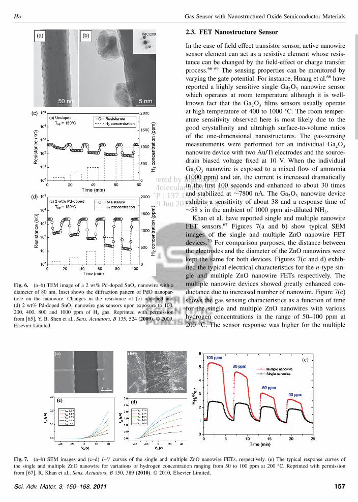
Delivered by Ingenta toInstitute of Molecular and Cell Biology
IP 13713239Tue 19 Jun 2012 003745
REVIEW
Ho Gas Sensor with Nanostructured Oxide Semiconductor Materials
(c)
(d)
(a) (b)
Fig 6 (andashb) TEM image of a 2 wt Pd-doped SnO2 nanowire with adiameter of 80 nm Inset shows the diffraction pattern of PdO nanopar-ticle on the nanowire Changes in the resistance of (c) undoped and(d) 2 wt Pd-doped SnO2 nanowire gas sensors upon exposure to 100200 400 800 and 1000 ppm of H2 gas Reprinted with permissionfrom [65] Y B Shen et al Sens Actuators B 135 524 (2009) copy 2009Elsevier Limited
(e)
Fig 7 (andashb) SEM images and (cndashd) IndashV curves of the single and multiple ZnO nanowire FETs respectively (e) The typical response curves ofthe single and multiple ZnO nanowire for variations of hydrogen concentration ranging from 50 to 100 ppm at 200 C Reprinted with permissionfrom [67] R Khan et al Sens Actuators B 150 389 (2010) copy 2010 Elsevier Limited
23 FET Nanostructure Sensor
In the case of field effect transistor sensor active nanowiresensor element can act as a resistive element whose resis-tance can be changed by the field-effect or charge transferprocess66ndash69 The sensing properties can be monitored byvarying the gate potential For instance Huang et al66 havereported a highly sensitive single Ga2O3 nanowire sensorwhich operates at room temperature although it is well-known fact that the Ga2O3 films sensors usually operateat high temperature of 400 to 1000 C The room temper-ature sensitivity observed here is most likely due to thegood crystallinity and ultrahigh surface-to-volume ratiosof the one-dimensional nanostructures The gas-sensingmeasurements were performed for an individual Ga2O3
nanowire device with two AuTi electrodes and the source-drain biased voltage fixed at 10 V When the individualGa2O3 nanowire is exposed to a mixed flow of ammonia(1000 ppm) and air the current is increased dramaticallyin the first 100 seconds and enhanced to about 30 timesand stabilized at sim7800 nA The Ga2O3 nanowire deviceexhibits a sensitivity of about 38 and a response time ofsim58 s in the ambient of 1000 ppm air-diluted NH3Khan et al have reported single and multiple nanowire
FET sensors67 Figures 7(a and b) show typical SEMimages of the single and multiple ZnO nanowire FETdevices70 For comparison purposes the distance betweenthe electrodes and the diameter of the ZnO nanowires werekept the same for both devices Figures 7(c and d) exhib-ited the typical electrical characteristics for the n-type sin-gle and multiple ZnO nanowire FETs respectively Themultiple nanowire devices showed greatly enhanced con-ductance due to increased number of nanowire Figure 7(e)shows the gas sensing characteristics as a function of timefor the single and multiple ZnO nanowires with varioushydrogen concentrations in the range of 50ndash100 ppm at200 C The sensor response was higher for the multiple
Sci Adv Mater 3 150ndash168 2011 157
Delivered by Ingenta toInstitute of Molecular and Cell Biology
IP 13713239Tue 19 Jun 2012 003745
REVIEW
Gas Sensor with Nanostructured Oxide Semiconductor Materials Ho
(a)
(b)
(c)
(d)
Fig 8 IndashVg curves before and after exposure to (a) 100-ppm NO2 and (b) 1 NH3 The response time of (c) 20 2 and 05 ppm NO2 and (d) 002NH3 Reprinted with permission from [68] C Li et al Appl Phys Lett 82 1613 (2003) copy 2003 American Institute of Physics
(a)
(b)
(c)
(d)
Fig 9 Schematic of (a) single and (b) multiple nanowire transistor structure where TiAu are deposited on nanowire-decorated SiSiO2 substrateas drain and source electrodes (c) IndashVg and (d) GGo versus time for the single and multi nanowire sensor device recorded at different NO2
concentrations Reprinted with permission from [72] D H Zhang et al Nano Lett 4 1919 (2004) copy 2004 American Chemical Society
158 Sci Adv Mater 3 150ndash168 2011
Delivered by Ingenta toInstitute of Molecular and Cell Biology
IP 13713239Tue 19 Jun 2012 003745
REVIEW
Ho Gas Sensor with Nanostructured Oxide Semiconductor Materials
ZnO nanowires than the response for the single ZnOnanowire over the entire range of hydrogen concentra-tion The multiple nanowires FET are made up of nano-junctions which acted as a potential barrier for electronflow The potential barrier decreased as the nanowire wasexposed to the reducing gas resulting in an increase inthe current flow The potential barrier modulation of mul-tiple nanowires was more efficient than the modulation ofthe surface depletion of the single ZnO nanowire in gassensing Therefore the potential barrier modulation in thenanojunctions caused the enhanced sensor response for themultiple nanowiresLi et al68 demonstrated the use of a single one-
dimensional nanowire FET sensor for high performanceroom temperature sensing The sensor is made up ofIn2O3 nanowires of diameter 10 nm and length 5 mwhich were placed between the source and drain elec-trodes with a silicon substrate as a back gate (Fig 8 inset)The as-fabricated In2O3 nanowire sensor devices exhib-ited typical n-type transistor characteristics The individualIn2O3 nanowire transistors sensors exhibited superior per-formance as such the sensitivity is of 106 for NO2 and 105
for NH3 which are four or five orders of magnitude betterthan results obtained from the thin-film based sensors71
Response times are as short as 5 s for 100-ppm NO2 and10 s for 1 NH3 The lowest detectable gas concentrationsare 05 ppm for NO2 and 002 for NH3
Furthermore the sensing and selectivity between dif-ferent gases can be studied by monitoring the currentdependence on the gate bias and the threshold voltageshift rendering a significant advantage over thin-film-based devices Figure 8(a) shows two currentndashgate volt-age (IndashVg) curves measured before and after exposure to100 ppm NO2 in argon with a constant source drain volt-age (Vds of minus03 V Both measurements suggest that theIn2O3 nanowires are n-type semiconductor as the con-ductance increase with gate bias There is also a pro-nounced shift in the threshold voltage from minus48 V before
(c)
Fig 10 (a) TEM of nanowires and nanobelts (b) Schematic view of device used for the in situ conductometric measurements under gas exposure andmetal deposition (c) Response of a pristine (dashed line) and Pd-functionalized (solid line) nanostructure to sequential oxygen and hydrogen pulses at473 K (top pane) and 543 K (bottom) Reprinted with permission from [73] A Kolmakov et al Nano Nano Lett 5 667 (2005) copy 2005 AmericanChemical Society
the exposure to 20 V after the exposure Adsorption ofoxidizing gases reduces the number of free electrons inthe n-type semiconductor and thus reduces the conductiv-ity Figure 8(b) shows two IndashVg curves before and afterexposing to diluted NH3 in Ar with Vds =minus03 V A largethreshold voltage shift from 248 V to 216 V is observedwith a maximum sensitivity of 105 at Vg = minus30 V ForNO2 concentrations of 20 2 and 05 ppm the responsetimes are determined to be 20 s 5 min and 10ndash12 minrespectively (Fig 8(c)) Figure 8(d) shows a response timeof about 2 min for 002 NH3 which is the lowest testedconcentration The limitation is imposed by the availabilityof highly diluted NH3 in air or argonZhang et al72 have demonstrated FET NO2 sensor down
to ppb levels based on both single and multiple In2O3
nanowires operating at room temperature as shown inschematic diagram Figures 9(a and b) Figure 9(c) showsthe conductance versus gate bias (Vg curves recorded inthe six different NO2 concentrations after exposure for20 min for single nanowire FET The threshold gate volt-age shifted rightward monotonically with the increasingNO2air concentration implying the gradual suppressionof carrier concentration of nanowire that scales linearlywith the absolute value of gate threshold As for the multinanowire FET the typical number of nanowires bridg-ing adjacent metal electrodes is estimated to be 100ndash200Figure 9(d) shows the sensing cycles of the multiwire FETdevice corresponding to NO2air concentrations of 5 1020 50 100 and 200 ppb The multiwire sensor showeda lower detection limit of 5 ppb compared to the 20 ppblimit of single nanowire sensors The room temperaturedetection limit is one of the lowest level ever reportedFurthermore selective detection of NH3 O2 CO and H2
is possible with this nanowire FET sensorKolmakov et al has demonstrated an enhanced 1-D
SnO2 nanostructure-based sensor with and without Pdnanoparticles decorated nanobelts (Fig 10(a))73 Thedeposited Pd works as catalysts for oxygen dissociation
Sci Adv Mater 3 150ndash168 2011 159
Delivered by Ingenta toInstitute of Molecular and Cell Biology
IP 13713239Tue 19 Jun 2012 003745
REVIEW
Gas Sensor with Nanostructured Oxide Semiconductor Materials Ho
Figure 10(b) shows the schematic view of device used forthe in situ conductometric FET measurements under gasexposure and metal deposition The sensing performanceof a SnO2 nanowire toward sequential oxygen and hydro-gen pulses at two different temperatures before (dashedcurves) and after (solid curves) Pd deposition is shownin Figure 10(c) Functionalizing the nanowire surface withPd leads to an enhancement in IDS response for both gasesand shorter response time Functionalizing the nanowiresurface with Pd leads to an enhancement in IDS responsefor both gases and to an increased speed of response Pdmetal nanoparticles grown on reduced n-SnO2 nanowiresand nanobelts were found to form Schottky-barrier likejunctions which locally deplete the nanostructure of elec-trons The improvements of sensitivity can be explained bythe combined ldquospillover effectrdquo of atomic oxygen formedcatalytically on the Pd particles then migrating onto thetin oxide and the back spillover effect in which weaklybound molecular oxygen migrate to the Pd and are cat-alytically dissociated Raising the temperature raises thevalue of IDS and shortens the response time of the sensorto O2 and H2 This effect is most prominent for oxygenfor which the nanostructure only becomes activated above543 K
3 DIRECTED ASSEMBLY OFNANOSTRUCTURE SENSORS
The application of nanostructures as building blocks forsensor can be achieved by implementing effective assem-bly and integration techniques to transfer the nanostructuresfrom growth substrates onto their respective device sub-strates Several methods have been developed to assembleone-dimensional nanostructures which include microflu-idic channel Langmuir-Blodgett blown bubble film self-assembled monolayers transfer printing alignment etcIn essence these approaches employ external forces toalign the nanostructures via wet or dry media In someapproaches multilayer alignment is possible while oth-ers allow selective spatial alignment in large-scale Thedevelopment of nanostructures based sensor generallyinvolves two processes First the assembly of nano-structures into highly integrated arrays with controlledorientation and spatial position second integration of inter-connects between nanostructures and the micro or macro-scopic subsystems
31 Transfer Printed Nanostructure Sensor
Transfer printing is a dry alignment technique wherebynanostructures are printed in contact or close proximityto the substrate allowing the nanostructures to be alignedin the same direction and in a predetermined densityThe nanostructures are grown on a substrate ldquostampsrdquoand then stamped ldquoprintedrdquo onto the receiving substrate
The receiving substrate can have pre deposited electrodesupon which nanostructures can be aligned The transferprinting deposition strategy has demonstrated to lead towell-defined and reproducible three-dimensional integratedcircuits structures of controlled nanowiresrsquo density andalignment over large substrate areas7475
Layer-by-layer assembly of nanowires for three-dimensional multifunctional electronics has been reportedby Javey et al74 The dry alignment process involves(i) optimized growth of designed nanowires by nanoclus-ter directed synthesis and(ii) patterned transfer of nanowires directly from ananowire growth substrate to a second device substrate viacontact printing (Figs 11(andashb))
In detail a photolithographically patterned device sub-strate is first firmly attached to a bench top and thenanowire growth substrate is placed face down in con-tact with the patterned device substrate A gentle man-ual pressure is then applied from the top followed bysliding the growth substrate by 1ndash3 mm before thegrowth substrate is removed Devices and circuits arethen fabricated on the printed arrays of nanowires usingconventional top-down lithography and metallization pro-cesses To fabricate a three-dimensional FET the con-tact printing of nanowires and device fabrication stepsare repeated several times along with the deposition ofSiO2 insulating layer in order to obtain vertically stackedelectronic layers (Figs 11(cndashd)) Another work which isalso reported by the same group is ordered arrays ofsingle-crystalline nano- and microwires of GaAs and InPwith well-controlled lengths widths and shape have beenfabricated over large areas from high quality bulk wafersby the use of traditional photolithography and anisotropicchemical wet etching75 Printing using elastomeric stampscan transfer these wire arrays to plastic substrates withexcellent retention of order and crystallographic orienta-tion of the wires Figure 11(e) shows the various printingconfiguration single to triple layers of nanowires patternsElectrical measurements on simple test structures demon-strate the high degree of mechanical flexibility of theresulting wire arrays on plastics The combination of topdown wire fabrication and transfer printing represents aneffective route to ultrahigh performance macroelectronicsystemsThe nanowires are observed to be cleanly printed
only at lithographically predefined locations FET device(Figs 14(cndashd)) The printed nanowires are aligned uni-formly across mm or larger scale with relatively highdensities (sim4 nanowirem) The monolithic integration ofindividual and parallel arrays of multifunctional and multi-layer circuits consists of up to 10 addressable vertical lay-ers This alignment methodology is applicable for the widerange of nanowire materials substrates and device designsFurthermore the simplicity and the low processing tem-perature requirement of the method makes it ideal for
160 Sci Adv Mater 3 150ndash168 2011
Delivered by Ingenta toInstitute of Molecular and Cell Biology
IP 13713239Tue 19 Jun 2012 003745
REVIEW
Ho Gas Sensor with Nanostructured Oxide Semiconductor Materials
(e)
Fig 11 Overview of 3D nanowire circuit integration (a) Contact printing of nanowire from growth substrate to prepatterned substrate (b) 3Dnanowire circuit is fabricated by the iteration of the contact printing device fabrication and separation layer deposition steps (c) Optical microscopeimage of 3D nanowire FETs (d) Dark field image shows a parallel array of nanowires aligned between source (S) drain (D) and top gate (G)electrodes Reprinted with permission from [74] A Javey et al Nano Lett 7 773 (2007) copy 2007 American Chemical Society (e) Images of singleto multiple layers of GaAs wire array which are transfer printed using elastomeric stamps Reprinted with permission from [75] Y G Sun and J ARogers Nano Lett 4 1953 (2004) copy 2004 American Chemical Society
achieving high performance three-dimensional integratedcircuitry with different functionalities in distinct layersTo demonstrate the potential of nanowire printing for
large-area sensor integration printed Si-nanowire arrayswere configured as H2 sensors P -type SiNWs were printedon Si substrates and two-terminal devices with Ni sili-cide contacts were fabricated77 The conductance of theSi nanowire array shows a strong dependence on the H2
exposure even at relatively low concentrations (250 ppm)It is worth noting that the nanowire printing method mayprovide a viable route toward the realization of electronicnoses and smart sensors capable of distinguishing chem-ical species while determining their concentrations Suchsensors may be envisioned through a large-scale integra-tion of different sensor components interfaced with signal-processing functions To achieve this goal heterogeneousassembly of nanowire materials with orthogonal sensitivityto different analytes is needed which may be achievedthrough a multistep nanowire printing process
32 Dielectrophoretic AssembledNanostructure Sensor
Dielectrophoresis (DEP) technique utilizes the dielectro-phoretic force acting on the particles to induce spatial
movement when exposed to a non uniform electric field inthe suspension medium The force depends on a numberof parameters such as the arrangement of the electrodethe frequency of the electric field and the resulting elec-tric field distribution as well as the dielectric propertiesof the particles and the surrounding medium By changingthese factors this force will pull the particle towards thehigher electric field region (positive DEP effect) or push ittowards the lower field region (negative DEP effect) DEPis a manipulation technique based on Maxwellrsquos classicalelectromagnetic field theory to allow controlled movementof particles in a controlled electric field between the presetelectrode structures The DEP technique has demonstratedthe potential for the construction of the nanosensors ornanoelectronic devices using as the nanostructured mate-rial as the building blocksJiang et al78 have reported work on manipulation of ZnO
nanorods by applying AC signals of suitable frequency andvoltage to provide non uniform electrical field on differentpatterns of electrode (Figs 12(andashb)) Similarly Li et al79
have proposed DEP assembly of nanowires onto interdigi-tated microelectrodes (Fig 12(c)) and mounted on micro-hotplate sensor platform (Fig 12(d))Template-assisted electrodeposition method and a
two-step thermal oxidation are employed Through
Sci Adv Mater 3 150ndash168 2011 161
Delivered by Ingenta toInstitute of Molecular and Cell Biology
IP 13713239Tue 19 Jun 2012 003745
REVIEW
Gas Sensor with Nanostructured Oxide Semiconductor Materials Ho
(a)
(b) (d)
(c)
Fig 12 (andashb) Low and high resolution SEM images of aligned ZnO nanowire in the interdigitated electrode array The voltage and the frequency ofthe applied electric field are 10 V and 5 kHz Reprinted with permission from [78] K W Jiang et al Sens Actuators B 134 79 (2008) copy 2008Elsevier Limited (c) Well dispersed and fairly aligned indiumtin nanowires bridged across the electrode array (d) Overview of the integrated sensorchip on micro-hotplate Reprinted with permission from [79] X P Li et al Sens Actuators B 148 404 (2010) copy 2008 Elsevier Limited
DEP(Sine waves)
Thermal andoxidationtreatment
Gas sensingmeasurement
Prefabrication of electrodes
Nanowire dispersion
Fig 13 Schematic of nanowire sensor integration nanowire suspension drop casting on interdigitated microelectrodes DEP assembly of metalnanowires alignment of nanowires on microelectrodes two-step thermal oxidation of nanowires and final integrated sensor chip The response curve ofthe various volatile organic compounds versus temperature Reprinted with permission from [80] T Jinkawa et al J Mol Catal A 155 193 (2000)copy 2008 Elsevier Limited
162 Sci Adv Mater 3 150ndash168 2011
Delivered by Ingenta toInstitute of Molecular and Cell Biology
IP 13713239Tue 19 Jun 2012 003745
REVIEW
Ho Gas Sensor with Nanostructured Oxide Semiconductor Materials
electrodeposition synthesis method one-dimensionalindium oxide tin oxide and indiumndashtin oxide nanowireswere successfully fabricated The nanowires are uniformand easy to process and assemble with good control ofchemical compositions The process flow of fabricatingnanowire sensor via DEP alignment process is shown inFigure 1380 The nanowires solution is prepared and dropcasted onto prefabricated interdigitated electrodes Thenanowires are observed to be randomly dispersed on theelectrodes The electrical field was generated by connect-ing a function generator to the interdigitated electrodeswhile a sinusoidal wave with a frequency of 5ndash6 MHzand peak-to-peak voltage of 6 V was applied during theDEP process At room temperature ethanol volatizedwithin minutes leaving nanowires aligned between theelectrode pairs Two thermal treatment processes werecarried out after the DEP assembly of nanowires to lowerthe contact resistance between the aligned nanowires andmicroelectrodes and increased the stability of the nanowireassembled First aligned metal nanowires were heated toabout 10 C below their melting points the temperaturevaried according to different material compositions Thebonding process was carried out in an inert nitrogenenvironment to prevent oxidation Next nanowires wereheated at the temperature just below the melting point ofthe respective material in an atmospheric environment for2 h The temperature was later raised to 400ndash500 C foranother 3 h to achieve full oxidation After the thermaland oxidation treatment the nanowire sensor chip wasready for electrical measurement and chemical response
ndash500
ndash400
ndash300
ndash200
ndash100
00
100
18E+10
22E+10
26E+10
30E+10
34E+10
38E+10
42E+10
0 600 1200 1800 2400 3000 3600 4200 4800
2500ppmH2
2000ppmH2
1154ppmH2
1000ppmH2
CDA CDA CDACDA
ndash350
ndash300
ndash250
ndash200
ndash150
ndash100
ndash50
00
50
100
40E+09
45E+09
50E+09
55E+09
60E+09
65E+09
70E+09
0 300 600 900 1200 1500 1800 2100 2400 2700
Time (s)
Time (s)
Res
ista
nce
(Ω)
Res
ista
nce
(Ω)
Sen
sitiv
ity (
)
Sen
sitiv
ity (
)
UV onUV on
UV off UV off
(a)
(c) (d)
(b)(e)
(f)
Fig 14 SEM images of (a) cotton textile substrate in low magnification (b) bare cotton fibres (c) ZnO nanorods-coated cotton fibres and (d) highmagnification images of ZnO nanorods on a cotton fibre Scale bar in the inset represents 100 nm Electrical responses of ZnO nanorods-on-cloth deviceto (e) various concentrations of H2 gas and (f) UV irradiation Clean dry air (CDA) was used to flush the chamber before and after each hydrogeninjection Experiments were performed in room temperature Reprinted with permission from [89] Z H Lim et al Sens Actuators B 151 121 (2010)copy 2010 Elsevier Limited
testing The sensor was investigated with different volatileorganic compounds The sensitivity of three alcohols isthe highest for methanol follow by ethanol isopropanolThese findings coincide with the number of methyl groupsin their chemical structure Two competitive dissociativereactions were proposed80 to explain the alcohol moleculesadsorbed on the oxide surface simply described as OndashHand CndashO bond-breaking processes where the former onehas a greater contribution to the resistance drop Thesensitivity order may relate to the preference of eachchemical over these two competitive reactions
4 NON-CONVENTIONAL SUBSTRATESENSOR
Technological and industrial difficulties in further minia-turization of devices have called for innovative ways toincorporate gadgets into articles of everyday life Thereare many sensors which have been fabricated on non con-ventional substrates namely the plastic textile and papersubstrate sensor The ability to fabricate sensor deviceson plastic substrates is important owing to the demandsof handheld portable consumer electronics Plastic sub-strates possess many attractive properties including bio-compatibility flexibility light weight shock resistancesoftness and transparency However plastics has low melt-ing point and they tend to deform or melt at tempera-tures of sim200 C This limits the synthesis temperatureof nanostructures directly on the plastic substrate Vari-ous ways to transfer the nanowires from donor substrate
Sci Adv Mater 3 150ndash168 2011 163
Delivered by Ingenta toInstitute of Molecular and Cell Biology
IP 13713239Tue 19 Jun 2012 003745
REVIEW
Gas Sensor with Nanostructured Oxide Semiconductor Materials Ho
to plastic substrate such as nanoimprint contact transferLangmuir Blogett etc have been developed In additionlow temperature synthesis processes have also been devel-oped to overcome this limitation Mc Alpine et al havereported plastic nanowire sensors based on Si nanowireswhich exhibit parts-per-billion sensitivity to NO2 a haz-ardous pollutant81
Another type of non conventional substrate sensor istextile Clothing is not only a necessity it also encom-passes a complete industry ranging from the down-to-earthbasics to the upmarket and chic Smart clothingtextiles arebecoming very popular in the past decade Smart textileswhich have been developed include silicon flexible skins
(b)
(a)
(d)
(c)
Source-meter
0
2E+09
4E+09
6E+09
8E+09
1E+10
12E+10
14E+10
16E+10
18E+10
I-V 1 I-V 2 I-V 3 I-V 4 I-V 5 Average
Res
ista
nce
(Ω)
Before After
(e)
(f)
(g)
Fig 15 SEM images of (a) low resolution ZnO-nanorods-coated textile with selected area (circled in red) for subsequent studies (b) the selected ZnOnanorods-coated yarns before stretching twisting and sonication (c) the same yarns after repeated stretching and twisting and (d) 5 minutes of watersonification (e) Schematic diagram of the electro-mechanical testing and (f) electrical properties before and after each stretching and twisting cycle(g) Electrical measurement of ZnO nanorods-on-cloth device while subjected to controlled stress cycles with a mechanical testing system Reprintedwith permission from [89] Z H Lim et al Sens Actuators B 151 121 (2010) copy 2010 Elsevier Limited
and organic transistors on textile fibers8283 Another type ofthe smart sensing textiles which uses piezo-resistive prop-erties has been developed The approach for fabricating thefabrics was to coat a thin layer of piezo-resistive materialssuch as polypyrrole or a mixture of rubbers and carbonson conventional fabrics to form fabric-based sensors84ndash86
The function of the developed sensors is similar to that offlexible strain gauges which can measure strains when theyare subjected to a tensile stress Other innovations whichare not actively explored are textiles which can detectenvironmental conditions which then react and adapt toenvironmental changes Furthermore smart textiles can bemade to measure and monitor the physiological conditions
164 Sci Adv Mater 3 150ndash168 2011
Delivered by Ingenta toInstitute of Molecular and Cell Biology
IP 13713239Tue 19 Jun 2012 003745
REVIEW
Ho Gas Sensor with Nanostructured Oxide Semiconductor Materials
of the wearer eg perspiration heartbeat etc Thus they canbe applied various healthcare systems
41 Textile Sensor
While the development of wearable devices has beenreported the incorporation of nano-materials into thedesigns has not been well explored In addition problemssuch as complex process mass production washabilityand wearing comforts needs to be well addressed The easeof synthesizing ZnO nanowires or nanorods on almost anysubstrates welcomes large-scale incorporation on textileZnO nano-structures are believed to be non-toxic and bio-safe87 allowing their direct usage in daily applicationsWhile the use of nano-materials in daily human activitiesraised questions on its potential health risks there is todate no in vivo evidence of toxicity of nano-particulateZnO88
29 nm
5 nm
1 μm1 μm
2 nm 5 μm
15Endash03
16Endash03
17Endash03
18Endash03
Time (s)
on off
1000 ppm
(a)
(c) (d)(f)
(b) (e)
15Endash03
16Endash03
16Endash03
17Endash03
17Endash03
18Endash03
18Endash03
150 250 350 450 550 650 0 150 300 450 600 750 900
Time (s)
Cur
rent
(m
A)
Cur
rent
(m
A)
on off
2000 ppm1500 ppm
1000 ppm2500 ppm
(g) (h)
Fig 16 (andashb) Low and (cndashd) high resolution TEM images of the nanobelts (e) Image of nanobelts sheet made without any addition of binder orreinforcement chemicals (f) Cross-sectional SEM image of the nanobelts sheet Current response of the sensor at (g) varying and (h) same ppm H2
concentration Reprinted with permission from [90] S Bela et al J Phys D Appl Phys 43 35401 (2010) copy 2010 Institute of Physics
SEM images of the textile and nanorods displayed inFigures 14(andashd) show radially oriented nanorods (diametersim80 nm) with hexagonal cross-section grown along thecylindrical fibres (diameter sim15 m)89 Length of thenanorods is sim1 m The nanorods form a uniform anddense coverage around entire lengths of the fibres to forma cross-linked semi-conductive textileThe conductive textile shows excellent multiple sens-
ing (gas and optical) performances at room temperature asshown in Figures 14(e) and (f) respectively In the presenceof hydrogen gas chemisorbed oxygen ions are reducedto release electrons to the conduction band of the ZnOsurface resulting in an increase in conductivity In addi-tion the reduction reaction decreases the surface densityof the oxygen adsorbate leading to a reduction in thewidth of the depletion region and the height of the sur-face potential barrier thus resulting in the decrease in theresistance of the sensor The mechanism for UV sensing
Sci Adv Mater 3 150ndash168 2011 165
Delivered by Ingenta toInstitute of Molecular and Cell Biology
IP 13713239Tue 19 Jun 2012 003745
REVIEW
Gas Sensor with Nanostructured Oxide Semiconductor Materials Ho
is similar to that of hydrogen sensing with holes fromthe photo-generated electronndashhole pairs playing the role ofremoving the adsorbed oxygen molecules insteadA notable feature of the ZnO nanorods-coated textile
device is its fine morphological and electrical stabilityunder multiple stress and washing cycles A critical chal-lenge of semi-conductive yarns and textile is its durabil-ity and constancy of electrical performance SEM analyses(Figs 15(andashd)) of the nanorods -on-cloth before and afterstretching twisting and ashing cycles show no cracks ordelamination of the nanorods from the fibres respectivelyFigure 15(e) shows a schematic of the electro-mechanicaltesting Electrical characterisations made before and aftereach stretching and twisting cycle (Fig 15(f)) show goodelectrical stability We further perform electrical conduc-tivity measurements while stretching and relaxing the tex-tile device in a controlled manner The semiconductingtextile exhibits a higher conductivity when stretched dueto tighter packing (increased contact junctions) of the ZnOnanorods-coated fibers Figure 15(g) shows the variation ofcurrent through the textile device as it underwent repeatedcycles of stress and relaxation When the stress is releasedconductivity falls and stabilises to the original state Againthe morphology of the nanorods-on-textile suffered nocracks of delamination or noticeable degradation after theelectromechanical testing
42 Free Standing Sheet Sensor
Another non conventional sensor substrate is a free stand-ing sheet of nanowire paper The nanostructures are tobe produced in gram quantities so that it can be easilymade into nanostructured paper sheet The thickness ofthe nanostructures sheet can be tuned according to theamount of nanostructures used After the filtering wascompleted a sheet of nanostructures was formed by sand-wiching between a metal calender which was pressed andheated to ensure the nanowires are well dried and bondedtogether to form the free-standing paperBela et al have been reported synthesis of hybrid
titanate and titania nanobelts (Figs 16(andashd)) in a large-scale quantity for gas sensing applications90 The nanobeltsare synthesized from TiO2 powder based on hydrolysis andion exchange of NaOH base and HCl acid respectivelySheets of as-synthesized nanobelts are used for electricaland gas sensing measurements Figure 16(e) shows thewhite nanobelts sheet made without any addition of binderor reinforcement chemicals Cross-sectional SEM image ofFigure 16(f) shows that the nanobelts sheet has a thicknessof sim15 m Figures 16(g and h) show the current responseof the sensor at varying and same ppm H2 concentra-tions respectively The measurements were conducted at anoperating temperature of 300 C From the graphs it is evi-dent that the introduction of hydrogen causes the resistanceof the sensor to reduce because of the injection of electrons
onto the surface of the metal-oxide nanostructures therebyimproving the conductivity of the bulk sensing capabili-ties The resistance increases as the concentration of H2 isvaried from 2500 to 1000 ppm The response time (90of Rair minusRgas is achieved within the first 40ndash50 s whilethe recovery time is 10ndash12 min From the Figure 7(c) itwas observed that the sensing response was rather stableand reversible In oxidizing atmosphere of 300 C ambi-ent oxygen is adsorbed on the surface of nanobelts mostlikely with a negative charge Subsequently with the intro-duction of a reducing H2 gas it reacts with the negativelycharged surface oxygen and decreases the resistance bythe injection of electron
5 CONCLUSIONS
There is an immense technological and scientific potentialsof nanostructured materials in nanodevice applicationsand already numerous nanomaterial based sensors usingvarious materials have been reported These oxide materi-als can be synthesized by various synthetic routes whichinclude both physical and chemical methods The poten-tial application of these nanostructures as sensor dependsgreatly on the ability to precisely control their dimensionchemical composition surface property phase purity andcrystal structure Sensor of various configurations bulktwo-terminal and FET device have been fabricated Theintegrability of the nanostructure sensor into microelec-tronic fabrication technology is an issue that needs tobe addressed Various ways to assemble nanowires so asto ease the device fabrication process have been devel-oped The recent advances in assembling larger and morecomplex nanowire sensor arrays and integrating them intonanoscale electronics can lead to exquisite sensor sys-tem performances These sensory systems can sensitivelytransduce gaschemicalbiological binding events into elec-tronicdigital signals which promise a sophisticated nano-electronics sensing system
6 FUTURE DIRECTIONS
Although nanomaterial based sensors are expected to out-perform their bulk component there are still many issuesand parameters to be studied and addressed Parameters tobe explored include structural and composition tuning aswell as doping and functionalization of surfaces to increaseselectivity sensitivity and materials integrity for long-termstability Other parameters such as limits of detection lim-its of quantification dynamic range response and recov-ery times and lifetime have to be studied and improvedas well The long-term reliability of a sensor is impor-tant since progressive drifts in the characteristics andorresponses of the sensors affect accurate testing and analy-sis The drift of the sensors are frequently related to highworking temperatures and exposure to chemically active
166 Sci Adv Mater 3 150ndash168 2011
Delivered by Ingenta toInstitute of Molecular and Cell Biology
IP 13713239Tue 19 Jun 2012 003745
REVIEW
Ho Gas Sensor with Nanostructured Oxide Semiconductor Materials
ambient gas Many other issues include aging grain-sizegrowth poisoning due to unknown chemical species dif-fusion processes within the device etc are to be addressedas wellThe future direction of the solid-state gas sensor is
towards integrated wirelessremote multi-purpose sens-ing high selectivity recognition of a specific biological orchemical species with ldquoelectronic-nose-tonguerdquo capabili-ties In addition development of miniaturized analyticalsensor which can be integrated in-line orand as standaloneportable sensors is paramount for industrial applicationsThe sensors can further be refined into a network of sensorarrays providing rapid screening monitoring and reportingsystem The data are collected in a database and form partof a feedback guidance system to the control algorithm inindustrial processes
Acknowledgments The work is supported by NationalUniversity of Singapore grant R-263-000-532-112Images used for the cover page are kindly contributed byZ H Lee and M Kevin multidisciplinary laboratory
References and Notes
1 D James S M Scott Z Ali and W T OrsquoHare Microchim Acta149 1 (2005)
2 C-D Kohlin Nanoelectronics and Information Technology editedby R Waser Wiley-VCH Berlin (2005) p 851
3 M E Franke T J Koplin and U Simon Small 2 36 (2006)4 A Kolmakov and M Moskovits Annu Rev Mater Res 34 151
(2004)5 A Mandelis and C Christofides Physics Chemistry and Technology
of Solid State Gas Sensor Devices Wiley-Interscience New York(1993)
6 P T Moseley Sens Actuators B 6 149 (1992)7 N M White and J D Turner Meas Sci Technol 8 1 (1997)8 D Kohl J Phys D 34 R125 (2001)9 N Pinna G Neri M Antonietti and M Niederberger Angew
Chem Int Ed 43 4345 (2004)10 L P Sun L H Huo H Zhao S Gao and J G Zhao Sens Actu-
ators B 114 387 (2006)11 Z F Liu T Yamazaki Y B Shen T Kikuta N Nakatani and
Y X Li Sens Actuators B 129 666 (2008)12 C S Rout A R Raju A Govindaraj and C N R Rao J Nanosci
Nanotechnol 7 1923 (2007)13 M S Arnold P Avouris Z W Pan and Z L Wang J Phys
Chem B 107 659 (2003)14 I Jimenez I M A Centeno R Scotti F Morazzoni A Cornet
and J R Morante J electrochem Soc 150 H72 (2003)15 S Semancik and R E Cavicchi Thin Solid Films 206 81 (1991)16 N S Baik G Sakai N Miura and N Yamazoe Sens Actuators B
63 74 (2000)17 M Ivanovskaya P Bogdanov G Faglia and G Sberveglieri Sens
Actuators B 68 344 (2000)18 K Ihokura and I Watson The Stannic Oxide Gas Sensormdash
Principles and Applications CRC Press Boa Raton (1994)19 K D Schierbaum U Weimar and W Gopel Sens Actuators B
7 1 (1992)20 G Korotcenkov Sens Actuators B 121 664 (2007)21 J G Lu P C Chang and Z Y Fan Mater Sci Eng 52 49 (2006)22 T Yamamoto and H Katayama-Yoshida Jpn J Appl Phys
38 L166 (1999)
23 J G Lu L P Zhu Z Z Ye F Zhuge B H Zhao D W MaL Wang and J Y Huang J Mater Sci 41 467 (2006)
24 J Zhong S Muthukumar Y Chen Y Lu H M Ng W Jiang andE L Garfunkel Appl Phys Lett 83 3401 (2003)
25 S Y Bae C W Na J H Kang and J Park J Phys Chem B109 2526 (2005)
26 S Y Li P Lin C Y Lee T Y Tseng and C J Huang J Phys DAppl Phys 37 2274 (2004)
27 D K Hwang H S Kim J H Lim J Y Oh J H Yang S J ParkK K Kim D C Look and Y S Park Appl Phys Lett 86 151917(2005)
28 W Lee M C Jeong S W Joo and J M Myoung Nanotechnology16 764 (2005)
29 W Lee M C Jeong and J M Myoung Appl Phys Lett 85 6167(2004)
30 D W Zeng C S Xie B L Zhu R Jiang X Chen W L SongJ B Wang and J Shi J Cryst Growth 266 511 (2004)
31 G Z Shen J H Cho J K Yoo G C Yi and C J Lee J PhysChem B 109 5491 (2005)
32 J B Cui and U J Gibson Appl Phys Lett 87 133108 (2005)33 C X Xu X W Sun Z L Dong M B Yu Y Z Xiong and J S
Chen Appl Phys Lett 86 173110 (2005)34 D A Schwartz K R Kittilstved and D R Gamelin Appl Phys
Lett 85 1395 (2004)35 C Ronning P X Gao Y Ding Z L Wang and D Schwen Appl
Phys Lett 84 783 (2004)36 A J Mieszawska R Jalilian G U Sumanasekera and F P
Zamborini Small 3 722 (2007)37 B Zhu K Li S Zhang S Wu and W Huang Prog Chem 20 48
(2008)38 J X Wang S S Xie and W Zhou MRS Bull 32 123 (2007)39 W Lu and C M Lieber J Phys D-Appl Phys 39 R387
(2006)40 X Wang and Y D Li Inorganic Chemistry 45 7522 (2006)41 Y Shen T Yamazaki Z Liu D Meng T Kikuta N Nakatani
M Saito and M Mori Sens Actuators B 135 524 (2009)42 A Kolmakov Y Zhang G Cheng and M Moskovits Adv Mater
15 997 (2003)43 X T Zhou J Q Hu C P Li D D D Ma C S Lee and S T
Lee Chem Phys Lett 369 220 (2003)44 T-J Hsueh C-L Hsu S-J Chang and I-C Chen Sens Actua-
tors B 126 473 (2007)45 Q Wan Q H Li Y J Chen T H Wang X L He J P Li and
C L Lin Appl Phys Lett 84 3654 (2004)46 G J Li X H Zhang and S Kawi Sens Actuators B 60 64 (1999)47 G J Li and S Kawi Talanta 45 759 (1998)48 E T H Tan G W Ho A S W Wong S Kawi and A T S Wee
Nanotechnology 19 255706 (2008)49 S Luo G Fu H Chen and Y Zhang Mater Chem Phys 109 541
(2008)50 C Y Wang M Ali T Kups C C Roehlig V Cimalla T Stauden
and O Ambacher Sens Actuators B 130 589 (2008)51 J Ahmed S Vaidya T Ahmad P Sujatha Devi D Das and A K
Ashok Mater Res Bull 43 264 (2008)52 J Kaur R Kumar and M C Bhatnagar Sens Actuators B
126 478 (2007)53 D Lutic M Strand A Lloyd-Spetz K Buchholt E Ieva P O
Kall and M Sanati Top Cata 45 105 (2007)54 A Teleki S E Pratsinis K Kalyanasundaram and P I Gouma
Sens Actuators B 119 683 (2006)55 X L Gou G X Wang X Y Kong D Wexler J Horvat J Yang
and J Park Chem Eur J 14 5996 (2008)56 X Feng Z J Li P Y Wang and Y F Zhou J Mat Sci 40 6597
(2005)57 J Chen L Xu W Li and X Gou Adv Mater 17 582 (2005)58 Z B Zhuang Q Peng J F Liu X Wang and Y D Li Inorg
Chem 46 5179 (2007)
Sci Adv Mater 3 150ndash168 2011 167
Delivered by Ingenta toInstitute of Molecular and Cell Biology
IP 13713239Tue 19 Jun 2012 003745
REVIEW
Gas Sensor with Nanostructured Oxide Semiconductor Materials Ho
59 M-W Ahn K-S Park J-H Heo D-W Kim K J Choi and J-GPark Sens Actuators B 138 168 (2009)
60 H T Wang B S Kang F Ren L C Tien P W Sadik D PNorton S J Pearton and J Lin Appl Phys A 81 1117 (2005)
61 B Wang L F Zhu Y H Yang N S Xu and G W Yang J PhysChem C 112 6643 (2008)
62 T H Jung S-I Kwon J-H Park D-G Lim Y-J Choi and J-GPark Appl Phys A 91 707 (2008)
63 S C Yeow W L Ong A S W Wong and G W Ho Sens Actu-ators B 143 295 (2009)
64 V V Sysoeva T Schneiderb J Goschnickb I KiselevbW Habichtb H Hahnb E Strelcovc and A Kolmakov Sens Actu-ators B 139 699 (2009)
65 Y B Shen T Yamazaki Z F Liu D Meng T Kikuta N NakataniM Saito and M Mori Sens Actuators B 135 524 (2009)
66 Y Huang S Yue Z Wang Q Wang C Shi Z Xu X D BaiC Tang and C Gu J Phys Chem B 110 796 (2006)
67 R Khan H-W Ra J T Kim W S Jang D Sharma and Y HIm Sens Actuators B 150 389 (2010)
68 C Li D H Zhang X L Liu S Han T Tang J Han and C ZhouAppl Phys Lett 82 1613 (2003)
69 Z Fan and J G Lu Appl Phys Lett 86 123510 (2005)70 Z Y Fan D W Wang P C Chang W Y Tseng and J G Lu
Appl Phys Lett 85 5923 (2004)71 M Liess Thin Solid Films 410 183 (2002)72 D H Zhang Z Q Liu C Li T Tang X L Liu S Han B Lei
and C W Zhou Nano Lett 4 1919 (2004)73 A Kolmakov D O Klenov Y Lilach S Stemmer and
M Moskovits Nano Lett 5 667 (2005)74 A Javey S W Nam R S Friedman H Yan and C M Lieber
Nano Lett 7 773 (2007)75 Y G Sun and J A Rogers Nano Lett 4 1953 (2004)
76 Z Fan J C Ho Z A Jacobson R Yerushalmi R L AlleyH Razavi and A Javey Nano Lett 8 20 (2008)
77 Z Y Fan J C Ho T Takahashi R Yerushalmi K Takei A CFord Y-L Chueh and A Javey Adv Mater 21 3730 (2009)
78 K W Jiang W J Liu L J Wan and J Zhang Sens Actuators B134 79 (2008)
79 X P Li E China H W Sun P Kurup and Z Y Gu Sens Actu-ators B 148 404 (2010)
80 T Jinkawa G Sakai J Tamaki N Miura and N Yamazoe J MolCatal A 155 193 (2000)
81 M C McAlpine H Ahmad D W Wang and J R Heath NatMater 6 379 (2007)
82 R B Katragadda and Y Xu A Novel Intelligent Textile TechnologyBased on Silicon Flexible Skins Electrical and Computer Engineer-ing Wayne State University Detroit Michigan USA ISWC (2005)pp 78ndash81
83 J B Lee and V Subramanian IEEE Trans Electron Devices 62 269(2005)
84 R Wijesiriwardana K Mitcham and T Dias Fibre-meshed trans-ducers based real time wearable physiological information moni-toring system Proceedings of the 8th International Symposium onWearable Computers ISWCrsquo04 (2004) pp 40ndash47
85 R Wijesiriwardana IEEE Sens J 6 571 (2006)86 E P Scilingo F Lorussi A Mazzoldi and D De Rossi Sens J
IEEE 3 460 (2003)87 J Zhou N Xu and Z L Wang Adv Mater 18 2432 (2006)88 G J Nohynek E K Dudour and M S Roberts Nanotechnology
21 136 (2008)89 Z H Lim Z X Chia M Kevin A S W Wong and G W Ho
Sens Actuators B 151 121 (2010)90 S Bela A S W Wong and G W Ho J Phys D Appl Phys
43 35401 (2010)
Received 4 November 2010 Accepted 20 January 2011
168 Sci Adv Mater 3 150ndash168 2011

Delivered by Ingenta toInstitute of Molecular and Cell Biology
IP 13713239Tue 19 Jun 2012 003745
REVIEW
Gas Sensor with Nanostructured Oxide Semiconductor Materials Ho
(a)
(b)
(c)
(d)
Fig 8 IndashVg curves before and after exposure to (a) 100-ppm NO2 and (b) 1 NH3 The response time of (c) 20 2 and 05 ppm NO2 and (d) 002NH3 Reprinted with permission from [68] C Li et al Appl Phys Lett 82 1613 (2003) copy 2003 American Institute of Physics
(a)
(b)
(c)
(d)
Fig 9 Schematic of (a) single and (b) multiple nanowire transistor structure where TiAu are deposited on nanowire-decorated SiSiO2 substrateas drain and source electrodes (c) IndashVg and (d) GGo versus time for the single and multi nanowire sensor device recorded at different NO2
concentrations Reprinted with permission from [72] D H Zhang et al Nano Lett 4 1919 (2004) copy 2004 American Chemical Society
158 Sci Adv Mater 3 150ndash168 2011
Delivered by Ingenta toInstitute of Molecular and Cell Biology
IP 13713239Tue 19 Jun 2012 003745
REVIEW
Ho Gas Sensor with Nanostructured Oxide Semiconductor Materials
ZnO nanowires than the response for the single ZnOnanowire over the entire range of hydrogen concentra-tion The multiple nanowires FET are made up of nano-junctions which acted as a potential barrier for electronflow The potential barrier decreased as the nanowire wasexposed to the reducing gas resulting in an increase inthe current flow The potential barrier modulation of mul-tiple nanowires was more efficient than the modulation ofthe surface depletion of the single ZnO nanowire in gassensing Therefore the potential barrier modulation in thenanojunctions caused the enhanced sensor response for themultiple nanowiresLi et al68 demonstrated the use of a single one-
dimensional nanowire FET sensor for high performanceroom temperature sensing The sensor is made up ofIn2O3 nanowires of diameter 10 nm and length 5 mwhich were placed between the source and drain elec-trodes with a silicon substrate as a back gate (Fig 8 inset)The as-fabricated In2O3 nanowire sensor devices exhib-ited typical n-type transistor characteristics The individualIn2O3 nanowire transistors sensors exhibited superior per-formance as such the sensitivity is of 106 for NO2 and 105
for NH3 which are four or five orders of magnitude betterthan results obtained from the thin-film based sensors71
Response times are as short as 5 s for 100-ppm NO2 and10 s for 1 NH3 The lowest detectable gas concentrationsare 05 ppm for NO2 and 002 for NH3
Furthermore the sensing and selectivity between dif-ferent gases can be studied by monitoring the currentdependence on the gate bias and the threshold voltageshift rendering a significant advantage over thin-film-based devices Figure 8(a) shows two currentndashgate volt-age (IndashVg) curves measured before and after exposure to100 ppm NO2 in argon with a constant source drain volt-age (Vds of minus03 V Both measurements suggest that theIn2O3 nanowires are n-type semiconductor as the con-ductance increase with gate bias There is also a pro-nounced shift in the threshold voltage from minus48 V before
(c)
Fig 10 (a) TEM of nanowires and nanobelts (b) Schematic view of device used for the in situ conductometric measurements under gas exposure andmetal deposition (c) Response of a pristine (dashed line) and Pd-functionalized (solid line) nanostructure to sequential oxygen and hydrogen pulses at473 K (top pane) and 543 K (bottom) Reprinted with permission from [73] A Kolmakov et al Nano Nano Lett 5 667 (2005) copy 2005 AmericanChemical Society
the exposure to 20 V after the exposure Adsorption ofoxidizing gases reduces the number of free electrons inthe n-type semiconductor and thus reduces the conductiv-ity Figure 8(b) shows two IndashVg curves before and afterexposing to diluted NH3 in Ar with Vds =minus03 V A largethreshold voltage shift from 248 V to 216 V is observedwith a maximum sensitivity of 105 at Vg = minus30 V ForNO2 concentrations of 20 2 and 05 ppm the responsetimes are determined to be 20 s 5 min and 10ndash12 minrespectively (Fig 8(c)) Figure 8(d) shows a response timeof about 2 min for 002 NH3 which is the lowest testedconcentration The limitation is imposed by the availabilityof highly diluted NH3 in air or argonZhang et al72 have demonstrated FET NO2 sensor down
to ppb levels based on both single and multiple In2O3
nanowires operating at room temperature as shown inschematic diagram Figures 9(a and b) Figure 9(c) showsthe conductance versus gate bias (Vg curves recorded inthe six different NO2 concentrations after exposure for20 min for single nanowire FET The threshold gate volt-age shifted rightward monotonically with the increasingNO2air concentration implying the gradual suppressionof carrier concentration of nanowire that scales linearlywith the absolute value of gate threshold As for the multinanowire FET the typical number of nanowires bridg-ing adjacent metal electrodes is estimated to be 100ndash200Figure 9(d) shows the sensing cycles of the multiwire FETdevice corresponding to NO2air concentrations of 5 1020 50 100 and 200 ppb The multiwire sensor showeda lower detection limit of 5 ppb compared to the 20 ppblimit of single nanowire sensors The room temperaturedetection limit is one of the lowest level ever reportedFurthermore selective detection of NH3 O2 CO and H2
is possible with this nanowire FET sensorKolmakov et al has demonstrated an enhanced 1-D
SnO2 nanostructure-based sensor with and without Pdnanoparticles decorated nanobelts (Fig 10(a))73 Thedeposited Pd works as catalysts for oxygen dissociation
Sci Adv Mater 3 150ndash168 2011 159
Delivered by Ingenta toInstitute of Molecular and Cell Biology
IP 13713239Tue 19 Jun 2012 003745
REVIEW
Gas Sensor with Nanostructured Oxide Semiconductor Materials Ho
Figure 10(b) shows the schematic view of device used forthe in situ conductometric FET measurements under gasexposure and metal deposition The sensing performanceof a SnO2 nanowire toward sequential oxygen and hydro-gen pulses at two different temperatures before (dashedcurves) and after (solid curves) Pd deposition is shownin Figure 10(c) Functionalizing the nanowire surface withPd leads to an enhancement in IDS response for both gasesand shorter response time Functionalizing the nanowiresurface with Pd leads to an enhancement in IDS responsefor both gases and to an increased speed of response Pdmetal nanoparticles grown on reduced n-SnO2 nanowiresand nanobelts were found to form Schottky-barrier likejunctions which locally deplete the nanostructure of elec-trons The improvements of sensitivity can be explained bythe combined ldquospillover effectrdquo of atomic oxygen formedcatalytically on the Pd particles then migrating onto thetin oxide and the back spillover effect in which weaklybound molecular oxygen migrate to the Pd and are cat-alytically dissociated Raising the temperature raises thevalue of IDS and shortens the response time of the sensorto O2 and H2 This effect is most prominent for oxygenfor which the nanostructure only becomes activated above543 K
3 DIRECTED ASSEMBLY OFNANOSTRUCTURE SENSORS
The application of nanostructures as building blocks forsensor can be achieved by implementing effective assem-bly and integration techniques to transfer the nanostructuresfrom growth substrates onto their respective device sub-strates Several methods have been developed to assembleone-dimensional nanostructures which include microflu-idic channel Langmuir-Blodgett blown bubble film self-assembled monolayers transfer printing alignment etcIn essence these approaches employ external forces toalign the nanostructures via wet or dry media In someapproaches multilayer alignment is possible while oth-ers allow selective spatial alignment in large-scale Thedevelopment of nanostructures based sensor generallyinvolves two processes First the assembly of nano-structures into highly integrated arrays with controlledorientation and spatial position second integration of inter-connects between nanostructures and the micro or macro-scopic subsystems
31 Transfer Printed Nanostructure Sensor
Transfer printing is a dry alignment technique wherebynanostructures are printed in contact or close proximityto the substrate allowing the nanostructures to be alignedin the same direction and in a predetermined densityThe nanostructures are grown on a substrate ldquostampsrdquoand then stamped ldquoprintedrdquo onto the receiving substrate
The receiving substrate can have pre deposited electrodesupon which nanostructures can be aligned The transferprinting deposition strategy has demonstrated to lead towell-defined and reproducible three-dimensional integratedcircuits structures of controlled nanowiresrsquo density andalignment over large substrate areas7475
Layer-by-layer assembly of nanowires for three-dimensional multifunctional electronics has been reportedby Javey et al74 The dry alignment process involves(i) optimized growth of designed nanowires by nanoclus-ter directed synthesis and(ii) patterned transfer of nanowires directly from ananowire growth substrate to a second device substrate viacontact printing (Figs 11(andashb))
In detail a photolithographically patterned device sub-strate is first firmly attached to a bench top and thenanowire growth substrate is placed face down in con-tact with the patterned device substrate A gentle man-ual pressure is then applied from the top followed bysliding the growth substrate by 1ndash3 mm before thegrowth substrate is removed Devices and circuits arethen fabricated on the printed arrays of nanowires usingconventional top-down lithography and metallization pro-cesses To fabricate a three-dimensional FET the con-tact printing of nanowires and device fabrication stepsare repeated several times along with the deposition ofSiO2 insulating layer in order to obtain vertically stackedelectronic layers (Figs 11(cndashd)) Another work which isalso reported by the same group is ordered arrays ofsingle-crystalline nano- and microwires of GaAs and InPwith well-controlled lengths widths and shape have beenfabricated over large areas from high quality bulk wafersby the use of traditional photolithography and anisotropicchemical wet etching75 Printing using elastomeric stampscan transfer these wire arrays to plastic substrates withexcellent retention of order and crystallographic orienta-tion of the wires Figure 11(e) shows the various printingconfiguration single to triple layers of nanowires patternsElectrical measurements on simple test structures demon-strate the high degree of mechanical flexibility of theresulting wire arrays on plastics The combination of topdown wire fabrication and transfer printing represents aneffective route to ultrahigh performance macroelectronicsystemsThe nanowires are observed to be cleanly printed
only at lithographically predefined locations FET device(Figs 14(cndashd)) The printed nanowires are aligned uni-formly across mm or larger scale with relatively highdensities (sim4 nanowirem) The monolithic integration ofindividual and parallel arrays of multifunctional and multi-layer circuits consists of up to 10 addressable vertical lay-ers This alignment methodology is applicable for the widerange of nanowire materials substrates and device designsFurthermore the simplicity and the low processing tem-perature requirement of the method makes it ideal for
160 Sci Adv Mater 3 150ndash168 2011
Delivered by Ingenta toInstitute of Molecular and Cell Biology
IP 13713239Tue 19 Jun 2012 003745
REVIEW
Ho Gas Sensor with Nanostructured Oxide Semiconductor Materials
(e)
Fig 11 Overview of 3D nanowire circuit integration (a) Contact printing of nanowire from growth substrate to prepatterned substrate (b) 3Dnanowire circuit is fabricated by the iteration of the contact printing device fabrication and separation layer deposition steps (c) Optical microscopeimage of 3D nanowire FETs (d) Dark field image shows a parallel array of nanowires aligned between source (S) drain (D) and top gate (G)electrodes Reprinted with permission from [74] A Javey et al Nano Lett 7 773 (2007) copy 2007 American Chemical Society (e) Images of singleto multiple layers of GaAs wire array which are transfer printed using elastomeric stamps Reprinted with permission from [75] Y G Sun and J ARogers Nano Lett 4 1953 (2004) copy 2004 American Chemical Society
achieving high performance three-dimensional integratedcircuitry with different functionalities in distinct layersTo demonstrate the potential of nanowire printing for
large-area sensor integration printed Si-nanowire arrayswere configured as H2 sensors P -type SiNWs were printedon Si substrates and two-terminal devices with Ni sili-cide contacts were fabricated77 The conductance of theSi nanowire array shows a strong dependence on the H2
exposure even at relatively low concentrations (250 ppm)It is worth noting that the nanowire printing method mayprovide a viable route toward the realization of electronicnoses and smart sensors capable of distinguishing chem-ical species while determining their concentrations Suchsensors may be envisioned through a large-scale integra-tion of different sensor components interfaced with signal-processing functions To achieve this goal heterogeneousassembly of nanowire materials with orthogonal sensitivityto different analytes is needed which may be achievedthrough a multistep nanowire printing process
32 Dielectrophoretic AssembledNanostructure Sensor
Dielectrophoresis (DEP) technique utilizes the dielectro-phoretic force acting on the particles to induce spatial
movement when exposed to a non uniform electric field inthe suspension medium The force depends on a numberof parameters such as the arrangement of the electrodethe frequency of the electric field and the resulting elec-tric field distribution as well as the dielectric propertiesof the particles and the surrounding medium By changingthese factors this force will pull the particle towards thehigher electric field region (positive DEP effect) or push ittowards the lower field region (negative DEP effect) DEPis a manipulation technique based on Maxwellrsquos classicalelectromagnetic field theory to allow controlled movementof particles in a controlled electric field between the presetelectrode structures The DEP technique has demonstratedthe potential for the construction of the nanosensors ornanoelectronic devices using as the nanostructured mate-rial as the building blocksJiang et al78 have reported work on manipulation of ZnO
nanorods by applying AC signals of suitable frequency andvoltage to provide non uniform electrical field on differentpatterns of electrode (Figs 12(andashb)) Similarly Li et al79
have proposed DEP assembly of nanowires onto interdigi-tated microelectrodes (Fig 12(c)) and mounted on micro-hotplate sensor platform (Fig 12(d))Template-assisted electrodeposition method and a
two-step thermal oxidation are employed Through
Sci Adv Mater 3 150ndash168 2011 161
Delivered by Ingenta toInstitute of Molecular and Cell Biology
IP 13713239Tue 19 Jun 2012 003745
REVIEW
Gas Sensor with Nanostructured Oxide Semiconductor Materials Ho
(a)
(b) (d)
(c)
Fig 12 (andashb) Low and high resolution SEM images of aligned ZnO nanowire in the interdigitated electrode array The voltage and the frequency ofthe applied electric field are 10 V and 5 kHz Reprinted with permission from [78] K W Jiang et al Sens Actuators B 134 79 (2008) copy 2008Elsevier Limited (c) Well dispersed and fairly aligned indiumtin nanowires bridged across the electrode array (d) Overview of the integrated sensorchip on micro-hotplate Reprinted with permission from [79] X P Li et al Sens Actuators B 148 404 (2010) copy 2008 Elsevier Limited
DEP(Sine waves)
Thermal andoxidationtreatment
Gas sensingmeasurement
Prefabrication of electrodes
Nanowire dispersion
Fig 13 Schematic of nanowire sensor integration nanowire suspension drop casting on interdigitated microelectrodes DEP assembly of metalnanowires alignment of nanowires on microelectrodes two-step thermal oxidation of nanowires and final integrated sensor chip The response curve ofthe various volatile organic compounds versus temperature Reprinted with permission from [80] T Jinkawa et al J Mol Catal A 155 193 (2000)copy 2008 Elsevier Limited
162 Sci Adv Mater 3 150ndash168 2011
Delivered by Ingenta toInstitute of Molecular and Cell Biology
IP 13713239Tue 19 Jun 2012 003745
REVIEW
Ho Gas Sensor with Nanostructured Oxide Semiconductor Materials
electrodeposition synthesis method one-dimensionalindium oxide tin oxide and indiumndashtin oxide nanowireswere successfully fabricated The nanowires are uniformand easy to process and assemble with good control ofchemical compositions The process flow of fabricatingnanowire sensor via DEP alignment process is shown inFigure 1380 The nanowires solution is prepared and dropcasted onto prefabricated interdigitated electrodes Thenanowires are observed to be randomly dispersed on theelectrodes The electrical field was generated by connect-ing a function generator to the interdigitated electrodeswhile a sinusoidal wave with a frequency of 5ndash6 MHzand peak-to-peak voltage of 6 V was applied during theDEP process At room temperature ethanol volatizedwithin minutes leaving nanowires aligned between theelectrode pairs Two thermal treatment processes werecarried out after the DEP assembly of nanowires to lowerthe contact resistance between the aligned nanowires andmicroelectrodes and increased the stability of the nanowireassembled First aligned metal nanowires were heated toabout 10 C below their melting points the temperaturevaried according to different material compositions Thebonding process was carried out in an inert nitrogenenvironment to prevent oxidation Next nanowires wereheated at the temperature just below the melting point ofthe respective material in an atmospheric environment for2 h The temperature was later raised to 400ndash500 C foranother 3 h to achieve full oxidation After the thermaland oxidation treatment the nanowire sensor chip wasready for electrical measurement and chemical response
ndash500
ndash400
ndash300
ndash200
ndash100
00
100
18E+10
22E+10
26E+10
30E+10
34E+10
38E+10
42E+10
0 600 1200 1800 2400 3000 3600 4200 4800
2500ppmH2
2000ppmH2
1154ppmH2
1000ppmH2
CDA CDA CDACDA
ndash350
ndash300
ndash250
ndash200
ndash150
ndash100
ndash50
00
50
100
40E+09
45E+09
50E+09
55E+09
60E+09
65E+09
70E+09
0 300 600 900 1200 1500 1800 2100 2400 2700
Time (s)
Time (s)
Res
ista
nce
(Ω)
Res
ista
nce
(Ω)
Sen
sitiv
ity (
)
Sen
sitiv
ity (
)
UV onUV on
UV off UV off
(a)
(c) (d)
(b)(e)
(f)
Fig 14 SEM images of (a) cotton textile substrate in low magnification (b) bare cotton fibres (c) ZnO nanorods-coated cotton fibres and (d) highmagnification images of ZnO nanorods on a cotton fibre Scale bar in the inset represents 100 nm Electrical responses of ZnO nanorods-on-cloth deviceto (e) various concentrations of H2 gas and (f) UV irradiation Clean dry air (CDA) was used to flush the chamber before and after each hydrogeninjection Experiments were performed in room temperature Reprinted with permission from [89] Z H Lim et al Sens Actuators B 151 121 (2010)copy 2010 Elsevier Limited
testing The sensor was investigated with different volatileorganic compounds The sensitivity of three alcohols isthe highest for methanol follow by ethanol isopropanolThese findings coincide with the number of methyl groupsin their chemical structure Two competitive dissociativereactions were proposed80 to explain the alcohol moleculesadsorbed on the oxide surface simply described as OndashHand CndashO bond-breaking processes where the former onehas a greater contribution to the resistance drop Thesensitivity order may relate to the preference of eachchemical over these two competitive reactions
4 NON-CONVENTIONAL SUBSTRATESENSOR
Technological and industrial difficulties in further minia-turization of devices have called for innovative ways toincorporate gadgets into articles of everyday life Thereare many sensors which have been fabricated on non con-ventional substrates namely the plastic textile and papersubstrate sensor The ability to fabricate sensor deviceson plastic substrates is important owing to the demandsof handheld portable consumer electronics Plastic sub-strates possess many attractive properties including bio-compatibility flexibility light weight shock resistancesoftness and transparency However plastics has low melt-ing point and they tend to deform or melt at tempera-tures of sim200 C This limits the synthesis temperatureof nanostructures directly on the plastic substrate Vari-ous ways to transfer the nanowires from donor substrate
Sci Adv Mater 3 150ndash168 2011 163
Delivered by Ingenta toInstitute of Molecular and Cell Biology
IP 13713239Tue 19 Jun 2012 003745
REVIEW
Gas Sensor with Nanostructured Oxide Semiconductor Materials Ho
to plastic substrate such as nanoimprint contact transferLangmuir Blogett etc have been developed In additionlow temperature synthesis processes have also been devel-oped to overcome this limitation Mc Alpine et al havereported plastic nanowire sensors based on Si nanowireswhich exhibit parts-per-billion sensitivity to NO2 a haz-ardous pollutant81
Another type of non conventional substrate sensor istextile Clothing is not only a necessity it also encom-passes a complete industry ranging from the down-to-earthbasics to the upmarket and chic Smart clothingtextiles arebecoming very popular in the past decade Smart textileswhich have been developed include silicon flexible skins
(b)
(a)
(d)
(c)
Source-meter
0
2E+09
4E+09
6E+09
8E+09
1E+10
12E+10
14E+10
16E+10
18E+10
I-V 1 I-V 2 I-V 3 I-V 4 I-V 5 Average
Res
ista
nce
(Ω)
Before After
(e)
(f)
(g)
Fig 15 SEM images of (a) low resolution ZnO-nanorods-coated textile with selected area (circled in red) for subsequent studies (b) the selected ZnOnanorods-coated yarns before stretching twisting and sonication (c) the same yarns after repeated stretching and twisting and (d) 5 minutes of watersonification (e) Schematic diagram of the electro-mechanical testing and (f) electrical properties before and after each stretching and twisting cycle(g) Electrical measurement of ZnO nanorods-on-cloth device while subjected to controlled stress cycles with a mechanical testing system Reprintedwith permission from [89] Z H Lim et al Sens Actuators B 151 121 (2010) copy 2010 Elsevier Limited
and organic transistors on textile fibers8283 Another type ofthe smart sensing textiles which uses piezo-resistive prop-erties has been developed The approach for fabricating thefabrics was to coat a thin layer of piezo-resistive materialssuch as polypyrrole or a mixture of rubbers and carbonson conventional fabrics to form fabric-based sensors84ndash86
The function of the developed sensors is similar to that offlexible strain gauges which can measure strains when theyare subjected to a tensile stress Other innovations whichare not actively explored are textiles which can detectenvironmental conditions which then react and adapt toenvironmental changes Furthermore smart textiles can bemade to measure and monitor the physiological conditions
164 Sci Adv Mater 3 150ndash168 2011
Delivered by Ingenta toInstitute of Molecular and Cell Biology
IP 13713239Tue 19 Jun 2012 003745
REVIEW
Ho Gas Sensor with Nanostructured Oxide Semiconductor Materials
of the wearer eg perspiration heartbeat etc Thus they canbe applied various healthcare systems
41 Textile Sensor
While the development of wearable devices has beenreported the incorporation of nano-materials into thedesigns has not been well explored In addition problemssuch as complex process mass production washabilityand wearing comforts needs to be well addressed The easeof synthesizing ZnO nanowires or nanorods on almost anysubstrates welcomes large-scale incorporation on textileZnO nano-structures are believed to be non-toxic and bio-safe87 allowing their direct usage in daily applicationsWhile the use of nano-materials in daily human activitiesraised questions on its potential health risks there is todate no in vivo evidence of toxicity of nano-particulateZnO88
29 nm
5 nm
1 μm1 μm
2 nm 5 μm
15Endash03
16Endash03
17Endash03
18Endash03
Time (s)
on off
1000 ppm
(a)
(c) (d)(f)
(b) (e)
15Endash03
16Endash03
16Endash03
17Endash03
17Endash03
18Endash03
18Endash03
150 250 350 450 550 650 0 150 300 450 600 750 900
Time (s)
Cur
rent
(m
A)
Cur
rent
(m
A)
on off
2000 ppm1500 ppm
1000 ppm2500 ppm
(g) (h)
Fig 16 (andashb) Low and (cndashd) high resolution TEM images of the nanobelts (e) Image of nanobelts sheet made without any addition of binder orreinforcement chemicals (f) Cross-sectional SEM image of the nanobelts sheet Current response of the sensor at (g) varying and (h) same ppm H2
concentration Reprinted with permission from [90] S Bela et al J Phys D Appl Phys 43 35401 (2010) copy 2010 Institute of Physics
SEM images of the textile and nanorods displayed inFigures 14(andashd) show radially oriented nanorods (diametersim80 nm) with hexagonal cross-section grown along thecylindrical fibres (diameter sim15 m)89 Length of thenanorods is sim1 m The nanorods form a uniform anddense coverage around entire lengths of the fibres to forma cross-linked semi-conductive textileThe conductive textile shows excellent multiple sens-
ing (gas and optical) performances at room temperature asshown in Figures 14(e) and (f) respectively In the presenceof hydrogen gas chemisorbed oxygen ions are reducedto release electrons to the conduction band of the ZnOsurface resulting in an increase in conductivity In addi-tion the reduction reaction decreases the surface densityof the oxygen adsorbate leading to a reduction in thewidth of the depletion region and the height of the sur-face potential barrier thus resulting in the decrease in theresistance of the sensor The mechanism for UV sensing
Sci Adv Mater 3 150ndash168 2011 165
Delivered by Ingenta toInstitute of Molecular and Cell Biology
IP 13713239Tue 19 Jun 2012 003745
REVIEW
Gas Sensor with Nanostructured Oxide Semiconductor Materials Ho
is similar to that of hydrogen sensing with holes fromthe photo-generated electronndashhole pairs playing the role ofremoving the adsorbed oxygen molecules insteadA notable feature of the ZnO nanorods-coated textile
device is its fine morphological and electrical stabilityunder multiple stress and washing cycles A critical chal-lenge of semi-conductive yarns and textile is its durabil-ity and constancy of electrical performance SEM analyses(Figs 15(andashd)) of the nanorods -on-cloth before and afterstretching twisting and ashing cycles show no cracks ordelamination of the nanorods from the fibres respectivelyFigure 15(e) shows a schematic of the electro-mechanicaltesting Electrical characterisations made before and aftereach stretching and twisting cycle (Fig 15(f)) show goodelectrical stability We further perform electrical conduc-tivity measurements while stretching and relaxing the tex-tile device in a controlled manner The semiconductingtextile exhibits a higher conductivity when stretched dueto tighter packing (increased contact junctions) of the ZnOnanorods-coated fibers Figure 15(g) shows the variation ofcurrent through the textile device as it underwent repeatedcycles of stress and relaxation When the stress is releasedconductivity falls and stabilises to the original state Againthe morphology of the nanorods-on-textile suffered nocracks of delamination or noticeable degradation after theelectromechanical testing
42 Free Standing Sheet Sensor
Another non conventional sensor substrate is a free stand-ing sheet of nanowire paper The nanostructures are tobe produced in gram quantities so that it can be easilymade into nanostructured paper sheet The thickness ofthe nanostructures sheet can be tuned according to theamount of nanostructures used After the filtering wascompleted a sheet of nanostructures was formed by sand-wiching between a metal calender which was pressed andheated to ensure the nanowires are well dried and bondedtogether to form the free-standing paperBela et al have been reported synthesis of hybrid
titanate and titania nanobelts (Figs 16(andashd)) in a large-scale quantity for gas sensing applications90 The nanobeltsare synthesized from TiO2 powder based on hydrolysis andion exchange of NaOH base and HCl acid respectivelySheets of as-synthesized nanobelts are used for electricaland gas sensing measurements Figure 16(e) shows thewhite nanobelts sheet made without any addition of binderor reinforcement chemicals Cross-sectional SEM image ofFigure 16(f) shows that the nanobelts sheet has a thicknessof sim15 m Figures 16(g and h) show the current responseof the sensor at varying and same ppm H2 concentra-tions respectively The measurements were conducted at anoperating temperature of 300 C From the graphs it is evi-dent that the introduction of hydrogen causes the resistanceof the sensor to reduce because of the injection of electrons
onto the surface of the metal-oxide nanostructures therebyimproving the conductivity of the bulk sensing capabili-ties The resistance increases as the concentration of H2 isvaried from 2500 to 1000 ppm The response time (90of Rair minusRgas is achieved within the first 40ndash50 s whilethe recovery time is 10ndash12 min From the Figure 7(c) itwas observed that the sensing response was rather stableand reversible In oxidizing atmosphere of 300 C ambi-ent oxygen is adsorbed on the surface of nanobelts mostlikely with a negative charge Subsequently with the intro-duction of a reducing H2 gas it reacts with the negativelycharged surface oxygen and decreases the resistance bythe injection of electron
5 CONCLUSIONS
There is an immense technological and scientific potentialsof nanostructured materials in nanodevice applicationsand already numerous nanomaterial based sensors usingvarious materials have been reported These oxide materi-als can be synthesized by various synthetic routes whichinclude both physical and chemical methods The poten-tial application of these nanostructures as sensor dependsgreatly on the ability to precisely control their dimensionchemical composition surface property phase purity andcrystal structure Sensor of various configurations bulktwo-terminal and FET device have been fabricated Theintegrability of the nanostructure sensor into microelec-tronic fabrication technology is an issue that needs tobe addressed Various ways to assemble nanowires so asto ease the device fabrication process have been devel-oped The recent advances in assembling larger and morecomplex nanowire sensor arrays and integrating them intonanoscale electronics can lead to exquisite sensor sys-tem performances These sensory systems can sensitivelytransduce gaschemicalbiological binding events into elec-tronicdigital signals which promise a sophisticated nano-electronics sensing system
6 FUTURE DIRECTIONS
Although nanomaterial based sensors are expected to out-perform their bulk component there are still many issuesand parameters to be studied and addressed Parameters tobe explored include structural and composition tuning aswell as doping and functionalization of surfaces to increaseselectivity sensitivity and materials integrity for long-termstability Other parameters such as limits of detection lim-its of quantification dynamic range response and recov-ery times and lifetime have to be studied and improvedas well The long-term reliability of a sensor is impor-tant since progressive drifts in the characteristics andorresponses of the sensors affect accurate testing and analy-sis The drift of the sensors are frequently related to highworking temperatures and exposure to chemically active
166 Sci Adv Mater 3 150ndash168 2011
Delivered by Ingenta toInstitute of Molecular and Cell Biology
IP 13713239Tue 19 Jun 2012 003745
REVIEW
Ho Gas Sensor with Nanostructured Oxide Semiconductor Materials
ambient gas Many other issues include aging grain-sizegrowth poisoning due to unknown chemical species dif-fusion processes within the device etc are to be addressedas wellThe future direction of the solid-state gas sensor is
towards integrated wirelessremote multi-purpose sens-ing high selectivity recognition of a specific biological orchemical species with ldquoelectronic-nose-tonguerdquo capabili-ties In addition development of miniaturized analyticalsensor which can be integrated in-line orand as standaloneportable sensors is paramount for industrial applicationsThe sensors can further be refined into a network of sensorarrays providing rapid screening monitoring and reportingsystem The data are collected in a database and form partof a feedback guidance system to the control algorithm inindustrial processes
Acknowledgments The work is supported by NationalUniversity of Singapore grant R-263-000-532-112Images used for the cover page are kindly contributed byZ H Lee and M Kevin multidisciplinary laboratory
References and Notes
1 D James S M Scott Z Ali and W T OrsquoHare Microchim Acta149 1 (2005)
2 C-D Kohlin Nanoelectronics and Information Technology editedby R Waser Wiley-VCH Berlin (2005) p 851
3 M E Franke T J Koplin and U Simon Small 2 36 (2006)4 A Kolmakov and M Moskovits Annu Rev Mater Res 34 151
(2004)5 A Mandelis and C Christofides Physics Chemistry and Technology
of Solid State Gas Sensor Devices Wiley-Interscience New York(1993)
6 P T Moseley Sens Actuators B 6 149 (1992)7 N M White and J D Turner Meas Sci Technol 8 1 (1997)8 D Kohl J Phys D 34 R125 (2001)9 N Pinna G Neri M Antonietti and M Niederberger Angew
Chem Int Ed 43 4345 (2004)10 L P Sun L H Huo H Zhao S Gao and J G Zhao Sens Actu-
ators B 114 387 (2006)11 Z F Liu T Yamazaki Y B Shen T Kikuta N Nakatani and
Y X Li Sens Actuators B 129 666 (2008)12 C S Rout A R Raju A Govindaraj and C N R Rao J Nanosci
Nanotechnol 7 1923 (2007)13 M S Arnold P Avouris Z W Pan and Z L Wang J Phys
Chem B 107 659 (2003)14 I Jimenez I M A Centeno R Scotti F Morazzoni A Cornet
and J R Morante J electrochem Soc 150 H72 (2003)15 S Semancik and R E Cavicchi Thin Solid Films 206 81 (1991)16 N S Baik G Sakai N Miura and N Yamazoe Sens Actuators B
63 74 (2000)17 M Ivanovskaya P Bogdanov G Faglia and G Sberveglieri Sens
Actuators B 68 344 (2000)18 K Ihokura and I Watson The Stannic Oxide Gas Sensormdash
Principles and Applications CRC Press Boa Raton (1994)19 K D Schierbaum U Weimar and W Gopel Sens Actuators B
7 1 (1992)20 G Korotcenkov Sens Actuators B 121 664 (2007)21 J G Lu P C Chang and Z Y Fan Mater Sci Eng 52 49 (2006)22 T Yamamoto and H Katayama-Yoshida Jpn J Appl Phys
38 L166 (1999)
23 J G Lu L P Zhu Z Z Ye F Zhuge B H Zhao D W MaL Wang and J Y Huang J Mater Sci 41 467 (2006)
24 J Zhong S Muthukumar Y Chen Y Lu H M Ng W Jiang andE L Garfunkel Appl Phys Lett 83 3401 (2003)
25 S Y Bae C W Na J H Kang and J Park J Phys Chem B109 2526 (2005)
26 S Y Li P Lin C Y Lee T Y Tseng and C J Huang J Phys DAppl Phys 37 2274 (2004)
27 D K Hwang H S Kim J H Lim J Y Oh J H Yang S J ParkK K Kim D C Look and Y S Park Appl Phys Lett 86 151917(2005)
28 W Lee M C Jeong S W Joo and J M Myoung Nanotechnology16 764 (2005)
29 W Lee M C Jeong and J M Myoung Appl Phys Lett 85 6167(2004)
30 D W Zeng C S Xie B L Zhu R Jiang X Chen W L SongJ B Wang and J Shi J Cryst Growth 266 511 (2004)
31 G Z Shen J H Cho J K Yoo G C Yi and C J Lee J PhysChem B 109 5491 (2005)
32 J B Cui and U J Gibson Appl Phys Lett 87 133108 (2005)33 C X Xu X W Sun Z L Dong M B Yu Y Z Xiong and J S
Chen Appl Phys Lett 86 173110 (2005)34 D A Schwartz K R Kittilstved and D R Gamelin Appl Phys
Lett 85 1395 (2004)35 C Ronning P X Gao Y Ding Z L Wang and D Schwen Appl
Phys Lett 84 783 (2004)36 A J Mieszawska R Jalilian G U Sumanasekera and F P
Zamborini Small 3 722 (2007)37 B Zhu K Li S Zhang S Wu and W Huang Prog Chem 20 48
(2008)38 J X Wang S S Xie and W Zhou MRS Bull 32 123 (2007)39 W Lu and C M Lieber J Phys D-Appl Phys 39 R387
(2006)40 X Wang and Y D Li Inorganic Chemistry 45 7522 (2006)41 Y Shen T Yamazaki Z Liu D Meng T Kikuta N Nakatani
M Saito and M Mori Sens Actuators B 135 524 (2009)42 A Kolmakov Y Zhang G Cheng and M Moskovits Adv Mater
15 997 (2003)43 X T Zhou J Q Hu C P Li D D D Ma C S Lee and S T
Lee Chem Phys Lett 369 220 (2003)44 T-J Hsueh C-L Hsu S-J Chang and I-C Chen Sens Actua-
tors B 126 473 (2007)45 Q Wan Q H Li Y J Chen T H Wang X L He J P Li and
C L Lin Appl Phys Lett 84 3654 (2004)46 G J Li X H Zhang and S Kawi Sens Actuators B 60 64 (1999)47 G J Li and S Kawi Talanta 45 759 (1998)48 E T H Tan G W Ho A S W Wong S Kawi and A T S Wee
Nanotechnology 19 255706 (2008)49 S Luo G Fu H Chen and Y Zhang Mater Chem Phys 109 541
(2008)50 C Y Wang M Ali T Kups C C Roehlig V Cimalla T Stauden
and O Ambacher Sens Actuators B 130 589 (2008)51 J Ahmed S Vaidya T Ahmad P Sujatha Devi D Das and A K
Ashok Mater Res Bull 43 264 (2008)52 J Kaur R Kumar and M C Bhatnagar Sens Actuators B
126 478 (2007)53 D Lutic M Strand A Lloyd-Spetz K Buchholt E Ieva P O
Kall and M Sanati Top Cata 45 105 (2007)54 A Teleki S E Pratsinis K Kalyanasundaram and P I Gouma
Sens Actuators B 119 683 (2006)55 X L Gou G X Wang X Y Kong D Wexler J Horvat J Yang
and J Park Chem Eur J 14 5996 (2008)56 X Feng Z J Li P Y Wang and Y F Zhou J Mat Sci 40 6597
(2005)57 J Chen L Xu W Li and X Gou Adv Mater 17 582 (2005)58 Z B Zhuang Q Peng J F Liu X Wang and Y D Li Inorg
Chem 46 5179 (2007)
Sci Adv Mater 3 150ndash168 2011 167
Delivered by Ingenta toInstitute of Molecular and Cell Biology
IP 13713239Tue 19 Jun 2012 003745
REVIEW
Gas Sensor with Nanostructured Oxide Semiconductor Materials Ho
59 M-W Ahn K-S Park J-H Heo D-W Kim K J Choi and J-GPark Sens Actuators B 138 168 (2009)
60 H T Wang B S Kang F Ren L C Tien P W Sadik D PNorton S J Pearton and J Lin Appl Phys A 81 1117 (2005)
61 B Wang L F Zhu Y H Yang N S Xu and G W Yang J PhysChem C 112 6643 (2008)
62 T H Jung S-I Kwon J-H Park D-G Lim Y-J Choi and J-GPark Appl Phys A 91 707 (2008)
63 S C Yeow W L Ong A S W Wong and G W Ho Sens Actu-ators B 143 295 (2009)
64 V V Sysoeva T Schneiderb J Goschnickb I KiselevbW Habichtb H Hahnb E Strelcovc and A Kolmakov Sens Actu-ators B 139 699 (2009)
65 Y B Shen T Yamazaki Z F Liu D Meng T Kikuta N NakataniM Saito and M Mori Sens Actuators B 135 524 (2009)
66 Y Huang S Yue Z Wang Q Wang C Shi Z Xu X D BaiC Tang and C Gu J Phys Chem B 110 796 (2006)
67 R Khan H-W Ra J T Kim W S Jang D Sharma and Y HIm Sens Actuators B 150 389 (2010)
68 C Li D H Zhang X L Liu S Han T Tang J Han and C ZhouAppl Phys Lett 82 1613 (2003)
69 Z Fan and J G Lu Appl Phys Lett 86 123510 (2005)70 Z Y Fan D W Wang P C Chang W Y Tseng and J G Lu
Appl Phys Lett 85 5923 (2004)71 M Liess Thin Solid Films 410 183 (2002)72 D H Zhang Z Q Liu C Li T Tang X L Liu S Han B Lei
and C W Zhou Nano Lett 4 1919 (2004)73 A Kolmakov D O Klenov Y Lilach S Stemmer and
M Moskovits Nano Lett 5 667 (2005)74 A Javey S W Nam R S Friedman H Yan and C M Lieber
Nano Lett 7 773 (2007)75 Y G Sun and J A Rogers Nano Lett 4 1953 (2004)
76 Z Fan J C Ho Z A Jacobson R Yerushalmi R L AlleyH Razavi and A Javey Nano Lett 8 20 (2008)
77 Z Y Fan J C Ho T Takahashi R Yerushalmi K Takei A CFord Y-L Chueh and A Javey Adv Mater 21 3730 (2009)
78 K W Jiang W J Liu L J Wan and J Zhang Sens Actuators B134 79 (2008)
79 X P Li E China H W Sun P Kurup and Z Y Gu Sens Actu-ators B 148 404 (2010)
80 T Jinkawa G Sakai J Tamaki N Miura and N Yamazoe J MolCatal A 155 193 (2000)
81 M C McAlpine H Ahmad D W Wang and J R Heath NatMater 6 379 (2007)
82 R B Katragadda and Y Xu A Novel Intelligent Textile TechnologyBased on Silicon Flexible Skins Electrical and Computer Engineer-ing Wayne State University Detroit Michigan USA ISWC (2005)pp 78ndash81
83 J B Lee and V Subramanian IEEE Trans Electron Devices 62 269(2005)
84 R Wijesiriwardana K Mitcham and T Dias Fibre-meshed trans-ducers based real time wearable physiological information moni-toring system Proceedings of the 8th International Symposium onWearable Computers ISWCrsquo04 (2004) pp 40ndash47
85 R Wijesiriwardana IEEE Sens J 6 571 (2006)86 E P Scilingo F Lorussi A Mazzoldi and D De Rossi Sens J
IEEE 3 460 (2003)87 J Zhou N Xu and Z L Wang Adv Mater 18 2432 (2006)88 G J Nohynek E K Dudour and M S Roberts Nanotechnology
21 136 (2008)89 Z H Lim Z X Chia M Kevin A S W Wong and G W Ho
Sens Actuators B 151 121 (2010)90 S Bela A S W Wong and G W Ho J Phys D Appl Phys
43 35401 (2010)
Received 4 November 2010 Accepted 20 January 2011
168 Sci Adv Mater 3 150ndash168 2011

Delivered by Ingenta toInstitute of Molecular and Cell Biology
IP 13713239Tue 19 Jun 2012 003745
REVIEW
Ho Gas Sensor with Nanostructured Oxide Semiconductor Materials
ZnO nanowires than the response for the single ZnOnanowire over the entire range of hydrogen concentra-tion The multiple nanowires FET are made up of nano-junctions which acted as a potential barrier for electronflow The potential barrier decreased as the nanowire wasexposed to the reducing gas resulting in an increase inthe current flow The potential barrier modulation of mul-tiple nanowires was more efficient than the modulation ofthe surface depletion of the single ZnO nanowire in gassensing Therefore the potential barrier modulation in thenanojunctions caused the enhanced sensor response for themultiple nanowiresLi et al68 demonstrated the use of a single one-
dimensional nanowire FET sensor for high performanceroom temperature sensing The sensor is made up ofIn2O3 nanowires of diameter 10 nm and length 5 mwhich were placed between the source and drain elec-trodes with a silicon substrate as a back gate (Fig 8 inset)The as-fabricated In2O3 nanowire sensor devices exhib-ited typical n-type transistor characteristics The individualIn2O3 nanowire transistors sensors exhibited superior per-formance as such the sensitivity is of 106 for NO2 and 105
for NH3 which are four or five orders of magnitude betterthan results obtained from the thin-film based sensors71
Response times are as short as 5 s for 100-ppm NO2 and10 s for 1 NH3 The lowest detectable gas concentrationsare 05 ppm for NO2 and 002 for NH3
Furthermore the sensing and selectivity between dif-ferent gases can be studied by monitoring the currentdependence on the gate bias and the threshold voltageshift rendering a significant advantage over thin-film-based devices Figure 8(a) shows two currentndashgate volt-age (IndashVg) curves measured before and after exposure to100 ppm NO2 in argon with a constant source drain volt-age (Vds of minus03 V Both measurements suggest that theIn2O3 nanowires are n-type semiconductor as the con-ductance increase with gate bias There is also a pro-nounced shift in the threshold voltage from minus48 V before
(c)
Fig 10 (a) TEM of nanowires and nanobelts (b) Schematic view of device used for the in situ conductometric measurements under gas exposure andmetal deposition (c) Response of a pristine (dashed line) and Pd-functionalized (solid line) nanostructure to sequential oxygen and hydrogen pulses at473 K (top pane) and 543 K (bottom) Reprinted with permission from [73] A Kolmakov et al Nano Nano Lett 5 667 (2005) copy 2005 AmericanChemical Society
the exposure to 20 V after the exposure Adsorption ofoxidizing gases reduces the number of free electrons inthe n-type semiconductor and thus reduces the conductiv-ity Figure 8(b) shows two IndashVg curves before and afterexposing to diluted NH3 in Ar with Vds =minus03 V A largethreshold voltage shift from 248 V to 216 V is observedwith a maximum sensitivity of 105 at Vg = minus30 V ForNO2 concentrations of 20 2 and 05 ppm the responsetimes are determined to be 20 s 5 min and 10ndash12 minrespectively (Fig 8(c)) Figure 8(d) shows a response timeof about 2 min for 002 NH3 which is the lowest testedconcentration The limitation is imposed by the availabilityof highly diluted NH3 in air or argonZhang et al72 have demonstrated FET NO2 sensor down
to ppb levels based on both single and multiple In2O3
nanowires operating at room temperature as shown inschematic diagram Figures 9(a and b) Figure 9(c) showsthe conductance versus gate bias (Vg curves recorded inthe six different NO2 concentrations after exposure for20 min for single nanowire FET The threshold gate volt-age shifted rightward monotonically with the increasingNO2air concentration implying the gradual suppressionof carrier concentration of nanowire that scales linearlywith the absolute value of gate threshold As for the multinanowire FET the typical number of nanowires bridg-ing adjacent metal electrodes is estimated to be 100ndash200Figure 9(d) shows the sensing cycles of the multiwire FETdevice corresponding to NO2air concentrations of 5 1020 50 100 and 200 ppb The multiwire sensor showeda lower detection limit of 5 ppb compared to the 20 ppblimit of single nanowire sensors The room temperaturedetection limit is one of the lowest level ever reportedFurthermore selective detection of NH3 O2 CO and H2
is possible with this nanowire FET sensorKolmakov et al has demonstrated an enhanced 1-D
SnO2 nanostructure-based sensor with and without Pdnanoparticles decorated nanobelts (Fig 10(a))73 Thedeposited Pd works as catalysts for oxygen dissociation
Sci Adv Mater 3 150ndash168 2011 159
Delivered by Ingenta toInstitute of Molecular and Cell Biology
IP 13713239Tue 19 Jun 2012 003745
REVIEW
Gas Sensor with Nanostructured Oxide Semiconductor Materials Ho
Figure 10(b) shows the schematic view of device used forthe in situ conductometric FET measurements under gasexposure and metal deposition The sensing performanceof a SnO2 nanowire toward sequential oxygen and hydro-gen pulses at two different temperatures before (dashedcurves) and after (solid curves) Pd deposition is shownin Figure 10(c) Functionalizing the nanowire surface withPd leads to an enhancement in IDS response for both gasesand shorter response time Functionalizing the nanowiresurface with Pd leads to an enhancement in IDS responsefor both gases and to an increased speed of response Pdmetal nanoparticles grown on reduced n-SnO2 nanowiresand nanobelts were found to form Schottky-barrier likejunctions which locally deplete the nanostructure of elec-trons The improvements of sensitivity can be explained bythe combined ldquospillover effectrdquo of atomic oxygen formedcatalytically on the Pd particles then migrating onto thetin oxide and the back spillover effect in which weaklybound molecular oxygen migrate to the Pd and are cat-alytically dissociated Raising the temperature raises thevalue of IDS and shortens the response time of the sensorto O2 and H2 This effect is most prominent for oxygenfor which the nanostructure only becomes activated above543 K
3 DIRECTED ASSEMBLY OFNANOSTRUCTURE SENSORS
The application of nanostructures as building blocks forsensor can be achieved by implementing effective assem-bly and integration techniques to transfer the nanostructuresfrom growth substrates onto their respective device sub-strates Several methods have been developed to assembleone-dimensional nanostructures which include microflu-idic channel Langmuir-Blodgett blown bubble film self-assembled monolayers transfer printing alignment etcIn essence these approaches employ external forces toalign the nanostructures via wet or dry media In someapproaches multilayer alignment is possible while oth-ers allow selective spatial alignment in large-scale Thedevelopment of nanostructures based sensor generallyinvolves two processes First the assembly of nano-structures into highly integrated arrays with controlledorientation and spatial position second integration of inter-connects between nanostructures and the micro or macro-scopic subsystems
31 Transfer Printed Nanostructure Sensor
Transfer printing is a dry alignment technique wherebynanostructures are printed in contact or close proximityto the substrate allowing the nanostructures to be alignedin the same direction and in a predetermined densityThe nanostructures are grown on a substrate ldquostampsrdquoand then stamped ldquoprintedrdquo onto the receiving substrate
The receiving substrate can have pre deposited electrodesupon which nanostructures can be aligned The transferprinting deposition strategy has demonstrated to lead towell-defined and reproducible three-dimensional integratedcircuits structures of controlled nanowiresrsquo density andalignment over large substrate areas7475
Layer-by-layer assembly of nanowires for three-dimensional multifunctional electronics has been reportedby Javey et al74 The dry alignment process involves(i) optimized growth of designed nanowires by nanoclus-ter directed synthesis and(ii) patterned transfer of nanowires directly from ananowire growth substrate to a second device substrate viacontact printing (Figs 11(andashb))
In detail a photolithographically patterned device sub-strate is first firmly attached to a bench top and thenanowire growth substrate is placed face down in con-tact with the patterned device substrate A gentle man-ual pressure is then applied from the top followed bysliding the growth substrate by 1ndash3 mm before thegrowth substrate is removed Devices and circuits arethen fabricated on the printed arrays of nanowires usingconventional top-down lithography and metallization pro-cesses To fabricate a three-dimensional FET the con-tact printing of nanowires and device fabrication stepsare repeated several times along with the deposition ofSiO2 insulating layer in order to obtain vertically stackedelectronic layers (Figs 11(cndashd)) Another work which isalso reported by the same group is ordered arrays ofsingle-crystalline nano- and microwires of GaAs and InPwith well-controlled lengths widths and shape have beenfabricated over large areas from high quality bulk wafersby the use of traditional photolithography and anisotropicchemical wet etching75 Printing using elastomeric stampscan transfer these wire arrays to plastic substrates withexcellent retention of order and crystallographic orienta-tion of the wires Figure 11(e) shows the various printingconfiguration single to triple layers of nanowires patternsElectrical measurements on simple test structures demon-strate the high degree of mechanical flexibility of theresulting wire arrays on plastics The combination of topdown wire fabrication and transfer printing represents aneffective route to ultrahigh performance macroelectronicsystemsThe nanowires are observed to be cleanly printed
only at lithographically predefined locations FET device(Figs 14(cndashd)) The printed nanowires are aligned uni-formly across mm or larger scale with relatively highdensities (sim4 nanowirem) The monolithic integration ofindividual and parallel arrays of multifunctional and multi-layer circuits consists of up to 10 addressable vertical lay-ers This alignment methodology is applicable for the widerange of nanowire materials substrates and device designsFurthermore the simplicity and the low processing tem-perature requirement of the method makes it ideal for
160 Sci Adv Mater 3 150ndash168 2011
Delivered by Ingenta toInstitute of Molecular and Cell Biology
IP 13713239Tue 19 Jun 2012 003745
REVIEW
Ho Gas Sensor with Nanostructured Oxide Semiconductor Materials
(e)
Fig 11 Overview of 3D nanowire circuit integration (a) Contact printing of nanowire from growth substrate to prepatterned substrate (b) 3Dnanowire circuit is fabricated by the iteration of the contact printing device fabrication and separation layer deposition steps (c) Optical microscopeimage of 3D nanowire FETs (d) Dark field image shows a parallel array of nanowires aligned between source (S) drain (D) and top gate (G)electrodes Reprinted with permission from [74] A Javey et al Nano Lett 7 773 (2007) copy 2007 American Chemical Society (e) Images of singleto multiple layers of GaAs wire array which are transfer printed using elastomeric stamps Reprinted with permission from [75] Y G Sun and J ARogers Nano Lett 4 1953 (2004) copy 2004 American Chemical Society
achieving high performance three-dimensional integratedcircuitry with different functionalities in distinct layersTo demonstrate the potential of nanowire printing for
large-area sensor integration printed Si-nanowire arrayswere configured as H2 sensors P -type SiNWs were printedon Si substrates and two-terminal devices with Ni sili-cide contacts were fabricated77 The conductance of theSi nanowire array shows a strong dependence on the H2
exposure even at relatively low concentrations (250 ppm)It is worth noting that the nanowire printing method mayprovide a viable route toward the realization of electronicnoses and smart sensors capable of distinguishing chem-ical species while determining their concentrations Suchsensors may be envisioned through a large-scale integra-tion of different sensor components interfaced with signal-processing functions To achieve this goal heterogeneousassembly of nanowire materials with orthogonal sensitivityto different analytes is needed which may be achievedthrough a multistep nanowire printing process
32 Dielectrophoretic AssembledNanostructure Sensor
Dielectrophoresis (DEP) technique utilizes the dielectro-phoretic force acting on the particles to induce spatial
movement when exposed to a non uniform electric field inthe suspension medium The force depends on a numberof parameters such as the arrangement of the electrodethe frequency of the electric field and the resulting elec-tric field distribution as well as the dielectric propertiesof the particles and the surrounding medium By changingthese factors this force will pull the particle towards thehigher electric field region (positive DEP effect) or push ittowards the lower field region (negative DEP effect) DEPis a manipulation technique based on Maxwellrsquos classicalelectromagnetic field theory to allow controlled movementof particles in a controlled electric field between the presetelectrode structures The DEP technique has demonstratedthe potential for the construction of the nanosensors ornanoelectronic devices using as the nanostructured mate-rial as the building blocksJiang et al78 have reported work on manipulation of ZnO
nanorods by applying AC signals of suitable frequency andvoltage to provide non uniform electrical field on differentpatterns of electrode (Figs 12(andashb)) Similarly Li et al79
have proposed DEP assembly of nanowires onto interdigi-tated microelectrodes (Fig 12(c)) and mounted on micro-hotplate sensor platform (Fig 12(d))Template-assisted electrodeposition method and a
two-step thermal oxidation are employed Through
Sci Adv Mater 3 150ndash168 2011 161
Delivered by Ingenta toInstitute of Molecular and Cell Biology
IP 13713239Tue 19 Jun 2012 003745
REVIEW
Gas Sensor with Nanostructured Oxide Semiconductor Materials Ho
(a)
(b) (d)
(c)
Fig 12 (andashb) Low and high resolution SEM images of aligned ZnO nanowire in the interdigitated electrode array The voltage and the frequency ofthe applied electric field are 10 V and 5 kHz Reprinted with permission from [78] K W Jiang et al Sens Actuators B 134 79 (2008) copy 2008Elsevier Limited (c) Well dispersed and fairly aligned indiumtin nanowires bridged across the electrode array (d) Overview of the integrated sensorchip on micro-hotplate Reprinted with permission from [79] X P Li et al Sens Actuators B 148 404 (2010) copy 2008 Elsevier Limited
DEP(Sine waves)
Thermal andoxidationtreatment
Gas sensingmeasurement
Prefabrication of electrodes
Nanowire dispersion
Fig 13 Schematic of nanowire sensor integration nanowire suspension drop casting on interdigitated microelectrodes DEP assembly of metalnanowires alignment of nanowires on microelectrodes two-step thermal oxidation of nanowires and final integrated sensor chip The response curve ofthe various volatile organic compounds versus temperature Reprinted with permission from [80] T Jinkawa et al J Mol Catal A 155 193 (2000)copy 2008 Elsevier Limited
162 Sci Adv Mater 3 150ndash168 2011
Delivered by Ingenta toInstitute of Molecular and Cell Biology
IP 13713239Tue 19 Jun 2012 003745
REVIEW
Ho Gas Sensor with Nanostructured Oxide Semiconductor Materials
electrodeposition synthesis method one-dimensionalindium oxide tin oxide and indiumndashtin oxide nanowireswere successfully fabricated The nanowires are uniformand easy to process and assemble with good control ofchemical compositions The process flow of fabricatingnanowire sensor via DEP alignment process is shown inFigure 1380 The nanowires solution is prepared and dropcasted onto prefabricated interdigitated electrodes Thenanowires are observed to be randomly dispersed on theelectrodes The electrical field was generated by connect-ing a function generator to the interdigitated electrodeswhile a sinusoidal wave with a frequency of 5ndash6 MHzand peak-to-peak voltage of 6 V was applied during theDEP process At room temperature ethanol volatizedwithin minutes leaving nanowires aligned between theelectrode pairs Two thermal treatment processes werecarried out after the DEP assembly of nanowires to lowerthe contact resistance between the aligned nanowires andmicroelectrodes and increased the stability of the nanowireassembled First aligned metal nanowires were heated toabout 10 C below their melting points the temperaturevaried according to different material compositions Thebonding process was carried out in an inert nitrogenenvironment to prevent oxidation Next nanowires wereheated at the temperature just below the melting point ofthe respective material in an atmospheric environment for2 h The temperature was later raised to 400ndash500 C foranother 3 h to achieve full oxidation After the thermaland oxidation treatment the nanowire sensor chip wasready for electrical measurement and chemical response
ndash500
ndash400
ndash300
ndash200
ndash100
00
100
18E+10
22E+10
26E+10
30E+10
34E+10
38E+10
42E+10
0 600 1200 1800 2400 3000 3600 4200 4800
2500ppmH2
2000ppmH2
1154ppmH2
1000ppmH2
CDA CDA CDACDA
ndash350
ndash300
ndash250
ndash200
ndash150
ndash100
ndash50
00
50
100
40E+09
45E+09
50E+09
55E+09
60E+09
65E+09
70E+09
0 300 600 900 1200 1500 1800 2100 2400 2700
Time (s)
Time (s)
Res
ista
nce
(Ω)
Res
ista
nce
(Ω)
Sen
sitiv
ity (
)
Sen
sitiv
ity (
)
UV onUV on
UV off UV off
(a)
(c) (d)
(b)(e)
(f)
Fig 14 SEM images of (a) cotton textile substrate in low magnification (b) bare cotton fibres (c) ZnO nanorods-coated cotton fibres and (d) highmagnification images of ZnO nanorods on a cotton fibre Scale bar in the inset represents 100 nm Electrical responses of ZnO nanorods-on-cloth deviceto (e) various concentrations of H2 gas and (f) UV irradiation Clean dry air (CDA) was used to flush the chamber before and after each hydrogeninjection Experiments were performed in room temperature Reprinted with permission from [89] Z H Lim et al Sens Actuators B 151 121 (2010)copy 2010 Elsevier Limited
testing The sensor was investigated with different volatileorganic compounds The sensitivity of three alcohols isthe highest for methanol follow by ethanol isopropanolThese findings coincide with the number of methyl groupsin their chemical structure Two competitive dissociativereactions were proposed80 to explain the alcohol moleculesadsorbed on the oxide surface simply described as OndashHand CndashO bond-breaking processes where the former onehas a greater contribution to the resistance drop Thesensitivity order may relate to the preference of eachchemical over these two competitive reactions
4 NON-CONVENTIONAL SUBSTRATESENSOR
Technological and industrial difficulties in further minia-turization of devices have called for innovative ways toincorporate gadgets into articles of everyday life Thereare many sensors which have been fabricated on non con-ventional substrates namely the plastic textile and papersubstrate sensor The ability to fabricate sensor deviceson plastic substrates is important owing to the demandsof handheld portable consumer electronics Plastic sub-strates possess many attractive properties including bio-compatibility flexibility light weight shock resistancesoftness and transparency However plastics has low melt-ing point and they tend to deform or melt at tempera-tures of sim200 C This limits the synthesis temperatureof nanostructures directly on the plastic substrate Vari-ous ways to transfer the nanowires from donor substrate
Sci Adv Mater 3 150ndash168 2011 163
Delivered by Ingenta toInstitute of Molecular and Cell Biology
IP 13713239Tue 19 Jun 2012 003745
REVIEW
Gas Sensor with Nanostructured Oxide Semiconductor Materials Ho
to plastic substrate such as nanoimprint contact transferLangmuir Blogett etc have been developed In additionlow temperature synthesis processes have also been devel-oped to overcome this limitation Mc Alpine et al havereported plastic nanowire sensors based on Si nanowireswhich exhibit parts-per-billion sensitivity to NO2 a haz-ardous pollutant81
Another type of non conventional substrate sensor istextile Clothing is not only a necessity it also encom-passes a complete industry ranging from the down-to-earthbasics to the upmarket and chic Smart clothingtextiles arebecoming very popular in the past decade Smart textileswhich have been developed include silicon flexible skins
(b)
(a)
(d)
(c)
Source-meter
0
2E+09
4E+09
6E+09
8E+09
1E+10
12E+10
14E+10
16E+10
18E+10
I-V 1 I-V 2 I-V 3 I-V 4 I-V 5 Average
Res
ista
nce
(Ω)
Before After
(e)
(f)
(g)
Fig 15 SEM images of (a) low resolution ZnO-nanorods-coated textile with selected area (circled in red) for subsequent studies (b) the selected ZnOnanorods-coated yarns before stretching twisting and sonication (c) the same yarns after repeated stretching and twisting and (d) 5 minutes of watersonification (e) Schematic diagram of the electro-mechanical testing and (f) electrical properties before and after each stretching and twisting cycle(g) Electrical measurement of ZnO nanorods-on-cloth device while subjected to controlled stress cycles with a mechanical testing system Reprintedwith permission from [89] Z H Lim et al Sens Actuators B 151 121 (2010) copy 2010 Elsevier Limited
and organic transistors on textile fibers8283 Another type ofthe smart sensing textiles which uses piezo-resistive prop-erties has been developed The approach for fabricating thefabrics was to coat a thin layer of piezo-resistive materialssuch as polypyrrole or a mixture of rubbers and carbonson conventional fabrics to form fabric-based sensors84ndash86
The function of the developed sensors is similar to that offlexible strain gauges which can measure strains when theyare subjected to a tensile stress Other innovations whichare not actively explored are textiles which can detectenvironmental conditions which then react and adapt toenvironmental changes Furthermore smart textiles can bemade to measure and monitor the physiological conditions
164 Sci Adv Mater 3 150ndash168 2011
Delivered by Ingenta toInstitute of Molecular and Cell Biology
IP 13713239Tue 19 Jun 2012 003745
REVIEW
Ho Gas Sensor with Nanostructured Oxide Semiconductor Materials
of the wearer eg perspiration heartbeat etc Thus they canbe applied various healthcare systems
41 Textile Sensor
While the development of wearable devices has beenreported the incorporation of nano-materials into thedesigns has not been well explored In addition problemssuch as complex process mass production washabilityand wearing comforts needs to be well addressed The easeof synthesizing ZnO nanowires or nanorods on almost anysubstrates welcomes large-scale incorporation on textileZnO nano-structures are believed to be non-toxic and bio-safe87 allowing their direct usage in daily applicationsWhile the use of nano-materials in daily human activitiesraised questions on its potential health risks there is todate no in vivo evidence of toxicity of nano-particulateZnO88
29 nm
5 nm
1 μm1 μm
2 nm 5 μm
15Endash03
16Endash03
17Endash03
18Endash03
Time (s)
on off
1000 ppm
(a)
(c) (d)(f)
(b) (e)
15Endash03
16Endash03
16Endash03
17Endash03
17Endash03
18Endash03
18Endash03
150 250 350 450 550 650 0 150 300 450 600 750 900
Time (s)
Cur
rent
(m
A)
Cur
rent
(m
A)
on off
2000 ppm1500 ppm
1000 ppm2500 ppm
(g) (h)
Fig 16 (andashb) Low and (cndashd) high resolution TEM images of the nanobelts (e) Image of nanobelts sheet made without any addition of binder orreinforcement chemicals (f) Cross-sectional SEM image of the nanobelts sheet Current response of the sensor at (g) varying and (h) same ppm H2
concentration Reprinted with permission from [90] S Bela et al J Phys D Appl Phys 43 35401 (2010) copy 2010 Institute of Physics
SEM images of the textile and nanorods displayed inFigures 14(andashd) show radially oriented nanorods (diametersim80 nm) with hexagonal cross-section grown along thecylindrical fibres (diameter sim15 m)89 Length of thenanorods is sim1 m The nanorods form a uniform anddense coverage around entire lengths of the fibres to forma cross-linked semi-conductive textileThe conductive textile shows excellent multiple sens-
ing (gas and optical) performances at room temperature asshown in Figures 14(e) and (f) respectively In the presenceof hydrogen gas chemisorbed oxygen ions are reducedto release electrons to the conduction band of the ZnOsurface resulting in an increase in conductivity In addi-tion the reduction reaction decreases the surface densityof the oxygen adsorbate leading to a reduction in thewidth of the depletion region and the height of the sur-face potential barrier thus resulting in the decrease in theresistance of the sensor The mechanism for UV sensing
Sci Adv Mater 3 150ndash168 2011 165
Delivered by Ingenta toInstitute of Molecular and Cell Biology
IP 13713239Tue 19 Jun 2012 003745
REVIEW
Gas Sensor with Nanostructured Oxide Semiconductor Materials Ho
is similar to that of hydrogen sensing with holes fromthe photo-generated electronndashhole pairs playing the role ofremoving the adsorbed oxygen molecules insteadA notable feature of the ZnO nanorods-coated textile
device is its fine morphological and electrical stabilityunder multiple stress and washing cycles A critical chal-lenge of semi-conductive yarns and textile is its durabil-ity and constancy of electrical performance SEM analyses(Figs 15(andashd)) of the nanorods -on-cloth before and afterstretching twisting and ashing cycles show no cracks ordelamination of the nanorods from the fibres respectivelyFigure 15(e) shows a schematic of the electro-mechanicaltesting Electrical characterisations made before and aftereach stretching and twisting cycle (Fig 15(f)) show goodelectrical stability We further perform electrical conduc-tivity measurements while stretching and relaxing the tex-tile device in a controlled manner The semiconductingtextile exhibits a higher conductivity when stretched dueto tighter packing (increased contact junctions) of the ZnOnanorods-coated fibers Figure 15(g) shows the variation ofcurrent through the textile device as it underwent repeatedcycles of stress and relaxation When the stress is releasedconductivity falls and stabilises to the original state Againthe morphology of the nanorods-on-textile suffered nocracks of delamination or noticeable degradation after theelectromechanical testing
42 Free Standing Sheet Sensor
Another non conventional sensor substrate is a free stand-ing sheet of nanowire paper The nanostructures are tobe produced in gram quantities so that it can be easilymade into nanostructured paper sheet The thickness ofthe nanostructures sheet can be tuned according to theamount of nanostructures used After the filtering wascompleted a sheet of nanostructures was formed by sand-wiching between a metal calender which was pressed andheated to ensure the nanowires are well dried and bondedtogether to form the free-standing paperBela et al have been reported synthesis of hybrid
titanate and titania nanobelts (Figs 16(andashd)) in a large-scale quantity for gas sensing applications90 The nanobeltsare synthesized from TiO2 powder based on hydrolysis andion exchange of NaOH base and HCl acid respectivelySheets of as-synthesized nanobelts are used for electricaland gas sensing measurements Figure 16(e) shows thewhite nanobelts sheet made without any addition of binderor reinforcement chemicals Cross-sectional SEM image ofFigure 16(f) shows that the nanobelts sheet has a thicknessof sim15 m Figures 16(g and h) show the current responseof the sensor at varying and same ppm H2 concentra-tions respectively The measurements were conducted at anoperating temperature of 300 C From the graphs it is evi-dent that the introduction of hydrogen causes the resistanceof the sensor to reduce because of the injection of electrons
onto the surface of the metal-oxide nanostructures therebyimproving the conductivity of the bulk sensing capabili-ties The resistance increases as the concentration of H2 isvaried from 2500 to 1000 ppm The response time (90of Rair minusRgas is achieved within the first 40ndash50 s whilethe recovery time is 10ndash12 min From the Figure 7(c) itwas observed that the sensing response was rather stableand reversible In oxidizing atmosphere of 300 C ambi-ent oxygen is adsorbed on the surface of nanobelts mostlikely with a negative charge Subsequently with the intro-duction of a reducing H2 gas it reacts with the negativelycharged surface oxygen and decreases the resistance bythe injection of electron
5 CONCLUSIONS
There is an immense technological and scientific potentialsof nanostructured materials in nanodevice applicationsand already numerous nanomaterial based sensors usingvarious materials have been reported These oxide materi-als can be synthesized by various synthetic routes whichinclude both physical and chemical methods The poten-tial application of these nanostructures as sensor dependsgreatly on the ability to precisely control their dimensionchemical composition surface property phase purity andcrystal structure Sensor of various configurations bulktwo-terminal and FET device have been fabricated Theintegrability of the nanostructure sensor into microelec-tronic fabrication technology is an issue that needs tobe addressed Various ways to assemble nanowires so asto ease the device fabrication process have been devel-oped The recent advances in assembling larger and morecomplex nanowire sensor arrays and integrating them intonanoscale electronics can lead to exquisite sensor sys-tem performances These sensory systems can sensitivelytransduce gaschemicalbiological binding events into elec-tronicdigital signals which promise a sophisticated nano-electronics sensing system
6 FUTURE DIRECTIONS
Although nanomaterial based sensors are expected to out-perform their bulk component there are still many issuesand parameters to be studied and addressed Parameters tobe explored include structural and composition tuning aswell as doping and functionalization of surfaces to increaseselectivity sensitivity and materials integrity for long-termstability Other parameters such as limits of detection lim-its of quantification dynamic range response and recov-ery times and lifetime have to be studied and improvedas well The long-term reliability of a sensor is impor-tant since progressive drifts in the characteristics andorresponses of the sensors affect accurate testing and analy-sis The drift of the sensors are frequently related to highworking temperatures and exposure to chemically active
166 Sci Adv Mater 3 150ndash168 2011
Delivered by Ingenta toInstitute of Molecular and Cell Biology
IP 13713239Tue 19 Jun 2012 003745
REVIEW
Ho Gas Sensor with Nanostructured Oxide Semiconductor Materials
ambient gas Many other issues include aging grain-sizegrowth poisoning due to unknown chemical species dif-fusion processes within the device etc are to be addressedas wellThe future direction of the solid-state gas sensor is
towards integrated wirelessremote multi-purpose sens-ing high selectivity recognition of a specific biological orchemical species with ldquoelectronic-nose-tonguerdquo capabili-ties In addition development of miniaturized analyticalsensor which can be integrated in-line orand as standaloneportable sensors is paramount for industrial applicationsThe sensors can further be refined into a network of sensorarrays providing rapid screening monitoring and reportingsystem The data are collected in a database and form partof a feedback guidance system to the control algorithm inindustrial processes
Acknowledgments The work is supported by NationalUniversity of Singapore grant R-263-000-532-112Images used for the cover page are kindly contributed byZ H Lee and M Kevin multidisciplinary laboratory
References and Notes
1 D James S M Scott Z Ali and W T OrsquoHare Microchim Acta149 1 (2005)
2 C-D Kohlin Nanoelectronics and Information Technology editedby R Waser Wiley-VCH Berlin (2005) p 851
3 M E Franke T J Koplin and U Simon Small 2 36 (2006)4 A Kolmakov and M Moskovits Annu Rev Mater Res 34 151
(2004)5 A Mandelis and C Christofides Physics Chemistry and Technology
of Solid State Gas Sensor Devices Wiley-Interscience New York(1993)
6 P T Moseley Sens Actuators B 6 149 (1992)7 N M White and J D Turner Meas Sci Technol 8 1 (1997)8 D Kohl J Phys D 34 R125 (2001)9 N Pinna G Neri M Antonietti and M Niederberger Angew
Chem Int Ed 43 4345 (2004)10 L P Sun L H Huo H Zhao S Gao and J G Zhao Sens Actu-
ators B 114 387 (2006)11 Z F Liu T Yamazaki Y B Shen T Kikuta N Nakatani and
Y X Li Sens Actuators B 129 666 (2008)12 C S Rout A R Raju A Govindaraj and C N R Rao J Nanosci
Nanotechnol 7 1923 (2007)13 M S Arnold P Avouris Z W Pan and Z L Wang J Phys
Chem B 107 659 (2003)14 I Jimenez I M A Centeno R Scotti F Morazzoni A Cornet
and J R Morante J electrochem Soc 150 H72 (2003)15 S Semancik and R E Cavicchi Thin Solid Films 206 81 (1991)16 N S Baik G Sakai N Miura and N Yamazoe Sens Actuators B
63 74 (2000)17 M Ivanovskaya P Bogdanov G Faglia and G Sberveglieri Sens
Actuators B 68 344 (2000)18 K Ihokura and I Watson The Stannic Oxide Gas Sensormdash
Principles and Applications CRC Press Boa Raton (1994)19 K D Schierbaum U Weimar and W Gopel Sens Actuators B
7 1 (1992)20 G Korotcenkov Sens Actuators B 121 664 (2007)21 J G Lu P C Chang and Z Y Fan Mater Sci Eng 52 49 (2006)22 T Yamamoto and H Katayama-Yoshida Jpn J Appl Phys
38 L166 (1999)
23 J G Lu L P Zhu Z Z Ye F Zhuge B H Zhao D W MaL Wang and J Y Huang J Mater Sci 41 467 (2006)
24 J Zhong S Muthukumar Y Chen Y Lu H M Ng W Jiang andE L Garfunkel Appl Phys Lett 83 3401 (2003)
25 S Y Bae C W Na J H Kang and J Park J Phys Chem B109 2526 (2005)
26 S Y Li P Lin C Y Lee T Y Tseng and C J Huang J Phys DAppl Phys 37 2274 (2004)
27 D K Hwang H S Kim J H Lim J Y Oh J H Yang S J ParkK K Kim D C Look and Y S Park Appl Phys Lett 86 151917(2005)
28 W Lee M C Jeong S W Joo and J M Myoung Nanotechnology16 764 (2005)
29 W Lee M C Jeong and J M Myoung Appl Phys Lett 85 6167(2004)
30 D W Zeng C S Xie B L Zhu R Jiang X Chen W L SongJ B Wang and J Shi J Cryst Growth 266 511 (2004)
31 G Z Shen J H Cho J K Yoo G C Yi and C J Lee J PhysChem B 109 5491 (2005)
32 J B Cui and U J Gibson Appl Phys Lett 87 133108 (2005)33 C X Xu X W Sun Z L Dong M B Yu Y Z Xiong and J S
Chen Appl Phys Lett 86 173110 (2005)34 D A Schwartz K R Kittilstved and D R Gamelin Appl Phys
Lett 85 1395 (2004)35 C Ronning P X Gao Y Ding Z L Wang and D Schwen Appl
Phys Lett 84 783 (2004)36 A J Mieszawska R Jalilian G U Sumanasekera and F P
Zamborini Small 3 722 (2007)37 B Zhu K Li S Zhang S Wu and W Huang Prog Chem 20 48
(2008)38 J X Wang S S Xie and W Zhou MRS Bull 32 123 (2007)39 W Lu and C M Lieber J Phys D-Appl Phys 39 R387
(2006)40 X Wang and Y D Li Inorganic Chemistry 45 7522 (2006)41 Y Shen T Yamazaki Z Liu D Meng T Kikuta N Nakatani
M Saito and M Mori Sens Actuators B 135 524 (2009)42 A Kolmakov Y Zhang G Cheng and M Moskovits Adv Mater
15 997 (2003)43 X T Zhou J Q Hu C P Li D D D Ma C S Lee and S T
Lee Chem Phys Lett 369 220 (2003)44 T-J Hsueh C-L Hsu S-J Chang and I-C Chen Sens Actua-
tors B 126 473 (2007)45 Q Wan Q H Li Y J Chen T H Wang X L He J P Li and
C L Lin Appl Phys Lett 84 3654 (2004)46 G J Li X H Zhang and S Kawi Sens Actuators B 60 64 (1999)47 G J Li and S Kawi Talanta 45 759 (1998)48 E T H Tan G W Ho A S W Wong S Kawi and A T S Wee
Nanotechnology 19 255706 (2008)49 S Luo G Fu H Chen and Y Zhang Mater Chem Phys 109 541
(2008)50 C Y Wang M Ali T Kups C C Roehlig V Cimalla T Stauden
and O Ambacher Sens Actuators B 130 589 (2008)51 J Ahmed S Vaidya T Ahmad P Sujatha Devi D Das and A K
Ashok Mater Res Bull 43 264 (2008)52 J Kaur R Kumar and M C Bhatnagar Sens Actuators B
126 478 (2007)53 D Lutic M Strand A Lloyd-Spetz K Buchholt E Ieva P O
Kall and M Sanati Top Cata 45 105 (2007)54 A Teleki S E Pratsinis K Kalyanasundaram and P I Gouma
Sens Actuators B 119 683 (2006)55 X L Gou G X Wang X Y Kong D Wexler J Horvat J Yang
and J Park Chem Eur J 14 5996 (2008)56 X Feng Z J Li P Y Wang and Y F Zhou J Mat Sci 40 6597
(2005)57 J Chen L Xu W Li and X Gou Adv Mater 17 582 (2005)58 Z B Zhuang Q Peng J F Liu X Wang and Y D Li Inorg
Chem 46 5179 (2007)
Sci Adv Mater 3 150ndash168 2011 167
Delivered by Ingenta toInstitute of Molecular and Cell Biology
IP 13713239Tue 19 Jun 2012 003745
REVIEW
Gas Sensor with Nanostructured Oxide Semiconductor Materials Ho
59 M-W Ahn K-S Park J-H Heo D-W Kim K J Choi and J-GPark Sens Actuators B 138 168 (2009)
60 H T Wang B S Kang F Ren L C Tien P W Sadik D PNorton S J Pearton and J Lin Appl Phys A 81 1117 (2005)
61 B Wang L F Zhu Y H Yang N S Xu and G W Yang J PhysChem C 112 6643 (2008)
62 T H Jung S-I Kwon J-H Park D-G Lim Y-J Choi and J-GPark Appl Phys A 91 707 (2008)
63 S C Yeow W L Ong A S W Wong and G W Ho Sens Actu-ators B 143 295 (2009)
64 V V Sysoeva T Schneiderb J Goschnickb I KiselevbW Habichtb H Hahnb E Strelcovc and A Kolmakov Sens Actu-ators B 139 699 (2009)
65 Y B Shen T Yamazaki Z F Liu D Meng T Kikuta N NakataniM Saito and M Mori Sens Actuators B 135 524 (2009)
66 Y Huang S Yue Z Wang Q Wang C Shi Z Xu X D BaiC Tang and C Gu J Phys Chem B 110 796 (2006)
67 R Khan H-W Ra J T Kim W S Jang D Sharma and Y HIm Sens Actuators B 150 389 (2010)
68 C Li D H Zhang X L Liu S Han T Tang J Han and C ZhouAppl Phys Lett 82 1613 (2003)
69 Z Fan and J G Lu Appl Phys Lett 86 123510 (2005)70 Z Y Fan D W Wang P C Chang W Y Tseng and J G Lu
Appl Phys Lett 85 5923 (2004)71 M Liess Thin Solid Films 410 183 (2002)72 D H Zhang Z Q Liu C Li T Tang X L Liu S Han B Lei
and C W Zhou Nano Lett 4 1919 (2004)73 A Kolmakov D O Klenov Y Lilach S Stemmer and
M Moskovits Nano Lett 5 667 (2005)74 A Javey S W Nam R S Friedman H Yan and C M Lieber
Nano Lett 7 773 (2007)75 Y G Sun and J A Rogers Nano Lett 4 1953 (2004)
76 Z Fan J C Ho Z A Jacobson R Yerushalmi R L AlleyH Razavi and A Javey Nano Lett 8 20 (2008)
77 Z Y Fan J C Ho T Takahashi R Yerushalmi K Takei A CFord Y-L Chueh and A Javey Adv Mater 21 3730 (2009)
78 K W Jiang W J Liu L J Wan and J Zhang Sens Actuators B134 79 (2008)
79 X P Li E China H W Sun P Kurup and Z Y Gu Sens Actu-ators B 148 404 (2010)
80 T Jinkawa G Sakai J Tamaki N Miura and N Yamazoe J MolCatal A 155 193 (2000)
81 M C McAlpine H Ahmad D W Wang and J R Heath NatMater 6 379 (2007)
82 R B Katragadda and Y Xu A Novel Intelligent Textile TechnologyBased on Silicon Flexible Skins Electrical and Computer Engineer-ing Wayne State University Detroit Michigan USA ISWC (2005)pp 78ndash81
83 J B Lee and V Subramanian IEEE Trans Electron Devices 62 269(2005)
84 R Wijesiriwardana K Mitcham and T Dias Fibre-meshed trans-ducers based real time wearable physiological information moni-toring system Proceedings of the 8th International Symposium onWearable Computers ISWCrsquo04 (2004) pp 40ndash47
85 R Wijesiriwardana IEEE Sens J 6 571 (2006)86 E P Scilingo F Lorussi A Mazzoldi and D De Rossi Sens J
IEEE 3 460 (2003)87 J Zhou N Xu and Z L Wang Adv Mater 18 2432 (2006)88 G J Nohynek E K Dudour and M S Roberts Nanotechnology
21 136 (2008)89 Z H Lim Z X Chia M Kevin A S W Wong and G W Ho
Sens Actuators B 151 121 (2010)90 S Bela A S W Wong and G W Ho J Phys D Appl Phys
43 35401 (2010)
Received 4 November 2010 Accepted 20 January 2011
168 Sci Adv Mater 3 150ndash168 2011

Delivered by Ingenta toInstitute of Molecular and Cell Biology
IP 13713239Tue 19 Jun 2012 003745
REVIEW
Gas Sensor with Nanostructured Oxide Semiconductor Materials Ho
Figure 10(b) shows the schematic view of device used forthe in situ conductometric FET measurements under gasexposure and metal deposition The sensing performanceof a SnO2 nanowire toward sequential oxygen and hydro-gen pulses at two different temperatures before (dashedcurves) and after (solid curves) Pd deposition is shownin Figure 10(c) Functionalizing the nanowire surface withPd leads to an enhancement in IDS response for both gasesand shorter response time Functionalizing the nanowiresurface with Pd leads to an enhancement in IDS responsefor both gases and to an increased speed of response Pdmetal nanoparticles grown on reduced n-SnO2 nanowiresand nanobelts were found to form Schottky-barrier likejunctions which locally deplete the nanostructure of elec-trons The improvements of sensitivity can be explained bythe combined ldquospillover effectrdquo of atomic oxygen formedcatalytically on the Pd particles then migrating onto thetin oxide and the back spillover effect in which weaklybound molecular oxygen migrate to the Pd and are cat-alytically dissociated Raising the temperature raises thevalue of IDS and shortens the response time of the sensorto O2 and H2 This effect is most prominent for oxygenfor which the nanostructure only becomes activated above543 K
3 DIRECTED ASSEMBLY OFNANOSTRUCTURE SENSORS
The application of nanostructures as building blocks forsensor can be achieved by implementing effective assem-bly and integration techniques to transfer the nanostructuresfrom growth substrates onto their respective device sub-strates Several methods have been developed to assembleone-dimensional nanostructures which include microflu-idic channel Langmuir-Blodgett blown bubble film self-assembled monolayers transfer printing alignment etcIn essence these approaches employ external forces toalign the nanostructures via wet or dry media In someapproaches multilayer alignment is possible while oth-ers allow selective spatial alignment in large-scale Thedevelopment of nanostructures based sensor generallyinvolves two processes First the assembly of nano-structures into highly integrated arrays with controlledorientation and spatial position second integration of inter-connects between nanostructures and the micro or macro-scopic subsystems
31 Transfer Printed Nanostructure Sensor
Transfer printing is a dry alignment technique wherebynanostructures are printed in contact or close proximityto the substrate allowing the nanostructures to be alignedin the same direction and in a predetermined densityThe nanostructures are grown on a substrate ldquostampsrdquoand then stamped ldquoprintedrdquo onto the receiving substrate
The receiving substrate can have pre deposited electrodesupon which nanostructures can be aligned The transferprinting deposition strategy has demonstrated to lead towell-defined and reproducible three-dimensional integratedcircuits structures of controlled nanowiresrsquo density andalignment over large substrate areas7475
Layer-by-layer assembly of nanowires for three-dimensional multifunctional electronics has been reportedby Javey et al74 The dry alignment process involves(i) optimized growth of designed nanowires by nanoclus-ter directed synthesis and(ii) patterned transfer of nanowires directly from ananowire growth substrate to a second device substrate viacontact printing (Figs 11(andashb))
In detail a photolithographically patterned device sub-strate is first firmly attached to a bench top and thenanowire growth substrate is placed face down in con-tact with the patterned device substrate A gentle man-ual pressure is then applied from the top followed bysliding the growth substrate by 1ndash3 mm before thegrowth substrate is removed Devices and circuits arethen fabricated on the printed arrays of nanowires usingconventional top-down lithography and metallization pro-cesses To fabricate a three-dimensional FET the con-tact printing of nanowires and device fabrication stepsare repeated several times along with the deposition ofSiO2 insulating layer in order to obtain vertically stackedelectronic layers (Figs 11(cndashd)) Another work which isalso reported by the same group is ordered arrays ofsingle-crystalline nano- and microwires of GaAs and InPwith well-controlled lengths widths and shape have beenfabricated over large areas from high quality bulk wafersby the use of traditional photolithography and anisotropicchemical wet etching75 Printing using elastomeric stampscan transfer these wire arrays to plastic substrates withexcellent retention of order and crystallographic orienta-tion of the wires Figure 11(e) shows the various printingconfiguration single to triple layers of nanowires patternsElectrical measurements on simple test structures demon-strate the high degree of mechanical flexibility of theresulting wire arrays on plastics The combination of topdown wire fabrication and transfer printing represents aneffective route to ultrahigh performance macroelectronicsystemsThe nanowires are observed to be cleanly printed
only at lithographically predefined locations FET device(Figs 14(cndashd)) The printed nanowires are aligned uni-formly across mm or larger scale with relatively highdensities (sim4 nanowirem) The monolithic integration ofindividual and parallel arrays of multifunctional and multi-layer circuits consists of up to 10 addressable vertical lay-ers This alignment methodology is applicable for the widerange of nanowire materials substrates and device designsFurthermore the simplicity and the low processing tem-perature requirement of the method makes it ideal for
160 Sci Adv Mater 3 150ndash168 2011
Delivered by Ingenta toInstitute of Molecular and Cell Biology
IP 13713239Tue 19 Jun 2012 003745
REVIEW
Ho Gas Sensor with Nanostructured Oxide Semiconductor Materials
(e)
Fig 11 Overview of 3D nanowire circuit integration (a) Contact printing of nanowire from growth substrate to prepatterned substrate (b) 3Dnanowire circuit is fabricated by the iteration of the contact printing device fabrication and separation layer deposition steps (c) Optical microscopeimage of 3D nanowire FETs (d) Dark field image shows a parallel array of nanowires aligned between source (S) drain (D) and top gate (G)electrodes Reprinted with permission from [74] A Javey et al Nano Lett 7 773 (2007) copy 2007 American Chemical Society (e) Images of singleto multiple layers of GaAs wire array which are transfer printed using elastomeric stamps Reprinted with permission from [75] Y G Sun and J ARogers Nano Lett 4 1953 (2004) copy 2004 American Chemical Society
achieving high performance three-dimensional integratedcircuitry with different functionalities in distinct layersTo demonstrate the potential of nanowire printing for
large-area sensor integration printed Si-nanowire arrayswere configured as H2 sensors P -type SiNWs were printedon Si substrates and two-terminal devices with Ni sili-cide contacts were fabricated77 The conductance of theSi nanowire array shows a strong dependence on the H2
exposure even at relatively low concentrations (250 ppm)It is worth noting that the nanowire printing method mayprovide a viable route toward the realization of electronicnoses and smart sensors capable of distinguishing chem-ical species while determining their concentrations Suchsensors may be envisioned through a large-scale integra-tion of different sensor components interfaced with signal-processing functions To achieve this goal heterogeneousassembly of nanowire materials with orthogonal sensitivityto different analytes is needed which may be achievedthrough a multistep nanowire printing process
32 Dielectrophoretic AssembledNanostructure Sensor
Dielectrophoresis (DEP) technique utilizes the dielectro-phoretic force acting on the particles to induce spatial
movement when exposed to a non uniform electric field inthe suspension medium The force depends on a numberof parameters such as the arrangement of the electrodethe frequency of the electric field and the resulting elec-tric field distribution as well as the dielectric propertiesof the particles and the surrounding medium By changingthese factors this force will pull the particle towards thehigher electric field region (positive DEP effect) or push ittowards the lower field region (negative DEP effect) DEPis a manipulation technique based on Maxwellrsquos classicalelectromagnetic field theory to allow controlled movementof particles in a controlled electric field between the presetelectrode structures The DEP technique has demonstratedthe potential for the construction of the nanosensors ornanoelectronic devices using as the nanostructured mate-rial as the building blocksJiang et al78 have reported work on manipulation of ZnO
nanorods by applying AC signals of suitable frequency andvoltage to provide non uniform electrical field on differentpatterns of electrode (Figs 12(andashb)) Similarly Li et al79
have proposed DEP assembly of nanowires onto interdigi-tated microelectrodes (Fig 12(c)) and mounted on micro-hotplate sensor platform (Fig 12(d))Template-assisted electrodeposition method and a
two-step thermal oxidation are employed Through
Sci Adv Mater 3 150ndash168 2011 161
Delivered by Ingenta toInstitute of Molecular and Cell Biology
IP 13713239Tue 19 Jun 2012 003745
REVIEW
Gas Sensor with Nanostructured Oxide Semiconductor Materials Ho
(a)
(b) (d)
(c)
Fig 12 (andashb) Low and high resolution SEM images of aligned ZnO nanowire in the interdigitated electrode array The voltage and the frequency ofthe applied electric field are 10 V and 5 kHz Reprinted with permission from [78] K W Jiang et al Sens Actuators B 134 79 (2008) copy 2008Elsevier Limited (c) Well dispersed and fairly aligned indiumtin nanowires bridged across the electrode array (d) Overview of the integrated sensorchip on micro-hotplate Reprinted with permission from [79] X P Li et al Sens Actuators B 148 404 (2010) copy 2008 Elsevier Limited
DEP(Sine waves)
Thermal andoxidationtreatment
Gas sensingmeasurement
Prefabrication of electrodes
Nanowire dispersion
Fig 13 Schematic of nanowire sensor integration nanowire suspension drop casting on interdigitated microelectrodes DEP assembly of metalnanowires alignment of nanowires on microelectrodes two-step thermal oxidation of nanowires and final integrated sensor chip The response curve ofthe various volatile organic compounds versus temperature Reprinted with permission from [80] T Jinkawa et al J Mol Catal A 155 193 (2000)copy 2008 Elsevier Limited
162 Sci Adv Mater 3 150ndash168 2011
Delivered by Ingenta toInstitute of Molecular and Cell Biology
IP 13713239Tue 19 Jun 2012 003745
REVIEW
Ho Gas Sensor with Nanostructured Oxide Semiconductor Materials
electrodeposition synthesis method one-dimensionalindium oxide tin oxide and indiumndashtin oxide nanowireswere successfully fabricated The nanowires are uniformand easy to process and assemble with good control ofchemical compositions The process flow of fabricatingnanowire sensor via DEP alignment process is shown inFigure 1380 The nanowires solution is prepared and dropcasted onto prefabricated interdigitated electrodes Thenanowires are observed to be randomly dispersed on theelectrodes The electrical field was generated by connect-ing a function generator to the interdigitated electrodeswhile a sinusoidal wave with a frequency of 5ndash6 MHzand peak-to-peak voltage of 6 V was applied during theDEP process At room temperature ethanol volatizedwithin minutes leaving nanowires aligned between theelectrode pairs Two thermal treatment processes werecarried out after the DEP assembly of nanowires to lowerthe contact resistance between the aligned nanowires andmicroelectrodes and increased the stability of the nanowireassembled First aligned metal nanowires were heated toabout 10 C below their melting points the temperaturevaried according to different material compositions Thebonding process was carried out in an inert nitrogenenvironment to prevent oxidation Next nanowires wereheated at the temperature just below the melting point ofthe respective material in an atmospheric environment for2 h The temperature was later raised to 400ndash500 C foranother 3 h to achieve full oxidation After the thermaland oxidation treatment the nanowire sensor chip wasready for electrical measurement and chemical response
ndash500
ndash400
ndash300
ndash200
ndash100
00
100
18E+10
22E+10
26E+10
30E+10
34E+10
38E+10
42E+10
0 600 1200 1800 2400 3000 3600 4200 4800
2500ppmH2
2000ppmH2
1154ppmH2
1000ppmH2
CDA CDA CDACDA
ndash350
ndash300
ndash250
ndash200
ndash150
ndash100
ndash50
00
50
100
40E+09
45E+09
50E+09
55E+09
60E+09
65E+09
70E+09
0 300 600 900 1200 1500 1800 2100 2400 2700
Time (s)
Time (s)
Res
ista
nce
(Ω)
Res
ista
nce
(Ω)
Sen
sitiv
ity (
)
Sen
sitiv
ity (
)
UV onUV on
UV off UV off
(a)
(c) (d)
(b)(e)
(f)
Fig 14 SEM images of (a) cotton textile substrate in low magnification (b) bare cotton fibres (c) ZnO nanorods-coated cotton fibres and (d) highmagnification images of ZnO nanorods on a cotton fibre Scale bar in the inset represents 100 nm Electrical responses of ZnO nanorods-on-cloth deviceto (e) various concentrations of H2 gas and (f) UV irradiation Clean dry air (CDA) was used to flush the chamber before and after each hydrogeninjection Experiments were performed in room temperature Reprinted with permission from [89] Z H Lim et al Sens Actuators B 151 121 (2010)copy 2010 Elsevier Limited
testing The sensor was investigated with different volatileorganic compounds The sensitivity of three alcohols isthe highest for methanol follow by ethanol isopropanolThese findings coincide with the number of methyl groupsin their chemical structure Two competitive dissociativereactions were proposed80 to explain the alcohol moleculesadsorbed on the oxide surface simply described as OndashHand CndashO bond-breaking processes where the former onehas a greater contribution to the resistance drop Thesensitivity order may relate to the preference of eachchemical over these two competitive reactions
4 NON-CONVENTIONAL SUBSTRATESENSOR
Technological and industrial difficulties in further minia-turization of devices have called for innovative ways toincorporate gadgets into articles of everyday life Thereare many sensors which have been fabricated on non con-ventional substrates namely the plastic textile and papersubstrate sensor The ability to fabricate sensor deviceson plastic substrates is important owing to the demandsof handheld portable consumer electronics Plastic sub-strates possess many attractive properties including bio-compatibility flexibility light weight shock resistancesoftness and transparency However plastics has low melt-ing point and they tend to deform or melt at tempera-tures of sim200 C This limits the synthesis temperatureof nanostructures directly on the plastic substrate Vari-ous ways to transfer the nanowires from donor substrate
Sci Adv Mater 3 150ndash168 2011 163
Delivered by Ingenta toInstitute of Molecular and Cell Biology
IP 13713239Tue 19 Jun 2012 003745
REVIEW
Gas Sensor with Nanostructured Oxide Semiconductor Materials Ho
to plastic substrate such as nanoimprint contact transferLangmuir Blogett etc have been developed In additionlow temperature synthesis processes have also been devel-oped to overcome this limitation Mc Alpine et al havereported plastic nanowire sensors based on Si nanowireswhich exhibit parts-per-billion sensitivity to NO2 a haz-ardous pollutant81
Another type of non conventional substrate sensor istextile Clothing is not only a necessity it also encom-passes a complete industry ranging from the down-to-earthbasics to the upmarket and chic Smart clothingtextiles arebecoming very popular in the past decade Smart textileswhich have been developed include silicon flexible skins
(b)
(a)
(d)
(c)
Source-meter
0
2E+09
4E+09
6E+09
8E+09
1E+10
12E+10
14E+10
16E+10
18E+10
I-V 1 I-V 2 I-V 3 I-V 4 I-V 5 Average
Res
ista
nce
(Ω)
Before After
(e)
(f)
(g)
Fig 15 SEM images of (a) low resolution ZnO-nanorods-coated textile with selected area (circled in red) for subsequent studies (b) the selected ZnOnanorods-coated yarns before stretching twisting and sonication (c) the same yarns after repeated stretching and twisting and (d) 5 minutes of watersonification (e) Schematic diagram of the electro-mechanical testing and (f) electrical properties before and after each stretching and twisting cycle(g) Electrical measurement of ZnO nanorods-on-cloth device while subjected to controlled stress cycles with a mechanical testing system Reprintedwith permission from [89] Z H Lim et al Sens Actuators B 151 121 (2010) copy 2010 Elsevier Limited
and organic transistors on textile fibers8283 Another type ofthe smart sensing textiles which uses piezo-resistive prop-erties has been developed The approach for fabricating thefabrics was to coat a thin layer of piezo-resistive materialssuch as polypyrrole or a mixture of rubbers and carbonson conventional fabrics to form fabric-based sensors84ndash86
The function of the developed sensors is similar to that offlexible strain gauges which can measure strains when theyare subjected to a tensile stress Other innovations whichare not actively explored are textiles which can detectenvironmental conditions which then react and adapt toenvironmental changes Furthermore smart textiles can bemade to measure and monitor the physiological conditions
164 Sci Adv Mater 3 150ndash168 2011
Delivered by Ingenta toInstitute of Molecular and Cell Biology
IP 13713239Tue 19 Jun 2012 003745
REVIEW
Ho Gas Sensor with Nanostructured Oxide Semiconductor Materials
of the wearer eg perspiration heartbeat etc Thus they canbe applied various healthcare systems
41 Textile Sensor
While the development of wearable devices has beenreported the incorporation of nano-materials into thedesigns has not been well explored In addition problemssuch as complex process mass production washabilityand wearing comforts needs to be well addressed The easeof synthesizing ZnO nanowires or nanorods on almost anysubstrates welcomes large-scale incorporation on textileZnO nano-structures are believed to be non-toxic and bio-safe87 allowing their direct usage in daily applicationsWhile the use of nano-materials in daily human activitiesraised questions on its potential health risks there is todate no in vivo evidence of toxicity of nano-particulateZnO88
29 nm
5 nm
1 μm1 μm
2 nm 5 μm
15Endash03
16Endash03
17Endash03
18Endash03
Time (s)
on off
1000 ppm
(a)
(c) (d)(f)
(b) (e)
15Endash03
16Endash03
16Endash03
17Endash03
17Endash03
18Endash03
18Endash03
150 250 350 450 550 650 0 150 300 450 600 750 900
Time (s)
Cur
rent
(m
A)
Cur
rent
(m
A)
on off
2000 ppm1500 ppm
1000 ppm2500 ppm
(g) (h)
Fig 16 (andashb) Low and (cndashd) high resolution TEM images of the nanobelts (e) Image of nanobelts sheet made without any addition of binder orreinforcement chemicals (f) Cross-sectional SEM image of the nanobelts sheet Current response of the sensor at (g) varying and (h) same ppm H2
concentration Reprinted with permission from [90] S Bela et al J Phys D Appl Phys 43 35401 (2010) copy 2010 Institute of Physics
SEM images of the textile and nanorods displayed inFigures 14(andashd) show radially oriented nanorods (diametersim80 nm) with hexagonal cross-section grown along thecylindrical fibres (diameter sim15 m)89 Length of thenanorods is sim1 m The nanorods form a uniform anddense coverage around entire lengths of the fibres to forma cross-linked semi-conductive textileThe conductive textile shows excellent multiple sens-
ing (gas and optical) performances at room temperature asshown in Figures 14(e) and (f) respectively In the presenceof hydrogen gas chemisorbed oxygen ions are reducedto release electrons to the conduction band of the ZnOsurface resulting in an increase in conductivity In addi-tion the reduction reaction decreases the surface densityof the oxygen adsorbate leading to a reduction in thewidth of the depletion region and the height of the sur-face potential barrier thus resulting in the decrease in theresistance of the sensor The mechanism for UV sensing
Sci Adv Mater 3 150ndash168 2011 165
Delivered by Ingenta toInstitute of Molecular and Cell Biology
IP 13713239Tue 19 Jun 2012 003745
REVIEW
Gas Sensor with Nanostructured Oxide Semiconductor Materials Ho
is similar to that of hydrogen sensing with holes fromthe photo-generated electronndashhole pairs playing the role ofremoving the adsorbed oxygen molecules insteadA notable feature of the ZnO nanorods-coated textile
device is its fine morphological and electrical stabilityunder multiple stress and washing cycles A critical chal-lenge of semi-conductive yarns and textile is its durabil-ity and constancy of electrical performance SEM analyses(Figs 15(andashd)) of the nanorods -on-cloth before and afterstretching twisting and ashing cycles show no cracks ordelamination of the nanorods from the fibres respectivelyFigure 15(e) shows a schematic of the electro-mechanicaltesting Electrical characterisations made before and aftereach stretching and twisting cycle (Fig 15(f)) show goodelectrical stability We further perform electrical conduc-tivity measurements while stretching and relaxing the tex-tile device in a controlled manner The semiconductingtextile exhibits a higher conductivity when stretched dueto tighter packing (increased contact junctions) of the ZnOnanorods-coated fibers Figure 15(g) shows the variation ofcurrent through the textile device as it underwent repeatedcycles of stress and relaxation When the stress is releasedconductivity falls and stabilises to the original state Againthe morphology of the nanorods-on-textile suffered nocracks of delamination or noticeable degradation after theelectromechanical testing
42 Free Standing Sheet Sensor
Another non conventional sensor substrate is a free stand-ing sheet of nanowire paper The nanostructures are tobe produced in gram quantities so that it can be easilymade into nanostructured paper sheet The thickness ofthe nanostructures sheet can be tuned according to theamount of nanostructures used After the filtering wascompleted a sheet of nanostructures was formed by sand-wiching between a metal calender which was pressed andheated to ensure the nanowires are well dried and bondedtogether to form the free-standing paperBela et al have been reported synthesis of hybrid
titanate and titania nanobelts (Figs 16(andashd)) in a large-scale quantity for gas sensing applications90 The nanobeltsare synthesized from TiO2 powder based on hydrolysis andion exchange of NaOH base and HCl acid respectivelySheets of as-synthesized nanobelts are used for electricaland gas sensing measurements Figure 16(e) shows thewhite nanobelts sheet made without any addition of binderor reinforcement chemicals Cross-sectional SEM image ofFigure 16(f) shows that the nanobelts sheet has a thicknessof sim15 m Figures 16(g and h) show the current responseof the sensor at varying and same ppm H2 concentra-tions respectively The measurements were conducted at anoperating temperature of 300 C From the graphs it is evi-dent that the introduction of hydrogen causes the resistanceof the sensor to reduce because of the injection of electrons
onto the surface of the metal-oxide nanostructures therebyimproving the conductivity of the bulk sensing capabili-ties The resistance increases as the concentration of H2 isvaried from 2500 to 1000 ppm The response time (90of Rair minusRgas is achieved within the first 40ndash50 s whilethe recovery time is 10ndash12 min From the Figure 7(c) itwas observed that the sensing response was rather stableand reversible In oxidizing atmosphere of 300 C ambi-ent oxygen is adsorbed on the surface of nanobelts mostlikely with a negative charge Subsequently with the intro-duction of a reducing H2 gas it reacts with the negativelycharged surface oxygen and decreases the resistance bythe injection of electron
5 CONCLUSIONS
There is an immense technological and scientific potentialsof nanostructured materials in nanodevice applicationsand already numerous nanomaterial based sensors usingvarious materials have been reported These oxide materi-als can be synthesized by various synthetic routes whichinclude both physical and chemical methods The poten-tial application of these nanostructures as sensor dependsgreatly on the ability to precisely control their dimensionchemical composition surface property phase purity andcrystal structure Sensor of various configurations bulktwo-terminal and FET device have been fabricated Theintegrability of the nanostructure sensor into microelec-tronic fabrication technology is an issue that needs tobe addressed Various ways to assemble nanowires so asto ease the device fabrication process have been devel-oped The recent advances in assembling larger and morecomplex nanowire sensor arrays and integrating them intonanoscale electronics can lead to exquisite sensor sys-tem performances These sensory systems can sensitivelytransduce gaschemicalbiological binding events into elec-tronicdigital signals which promise a sophisticated nano-electronics sensing system
6 FUTURE DIRECTIONS
Although nanomaterial based sensors are expected to out-perform their bulk component there are still many issuesand parameters to be studied and addressed Parameters tobe explored include structural and composition tuning aswell as doping and functionalization of surfaces to increaseselectivity sensitivity and materials integrity for long-termstability Other parameters such as limits of detection lim-its of quantification dynamic range response and recov-ery times and lifetime have to be studied and improvedas well The long-term reliability of a sensor is impor-tant since progressive drifts in the characteristics andorresponses of the sensors affect accurate testing and analy-sis The drift of the sensors are frequently related to highworking temperatures and exposure to chemically active
166 Sci Adv Mater 3 150ndash168 2011
Delivered by Ingenta toInstitute of Molecular and Cell Biology
IP 13713239Tue 19 Jun 2012 003745
REVIEW
Ho Gas Sensor with Nanostructured Oxide Semiconductor Materials
ambient gas Many other issues include aging grain-sizegrowth poisoning due to unknown chemical species dif-fusion processes within the device etc are to be addressedas wellThe future direction of the solid-state gas sensor is
towards integrated wirelessremote multi-purpose sens-ing high selectivity recognition of a specific biological orchemical species with ldquoelectronic-nose-tonguerdquo capabili-ties In addition development of miniaturized analyticalsensor which can be integrated in-line orand as standaloneportable sensors is paramount for industrial applicationsThe sensors can further be refined into a network of sensorarrays providing rapid screening monitoring and reportingsystem The data are collected in a database and form partof a feedback guidance system to the control algorithm inindustrial processes
Acknowledgments The work is supported by NationalUniversity of Singapore grant R-263-000-532-112Images used for the cover page are kindly contributed byZ H Lee and M Kevin multidisciplinary laboratory
References and Notes
1 D James S M Scott Z Ali and W T OrsquoHare Microchim Acta149 1 (2005)
2 C-D Kohlin Nanoelectronics and Information Technology editedby R Waser Wiley-VCH Berlin (2005) p 851
3 M E Franke T J Koplin and U Simon Small 2 36 (2006)4 A Kolmakov and M Moskovits Annu Rev Mater Res 34 151
(2004)5 A Mandelis and C Christofides Physics Chemistry and Technology
of Solid State Gas Sensor Devices Wiley-Interscience New York(1993)
6 P T Moseley Sens Actuators B 6 149 (1992)7 N M White and J D Turner Meas Sci Technol 8 1 (1997)8 D Kohl J Phys D 34 R125 (2001)9 N Pinna G Neri M Antonietti and M Niederberger Angew
Chem Int Ed 43 4345 (2004)10 L P Sun L H Huo H Zhao S Gao and J G Zhao Sens Actu-
ators B 114 387 (2006)11 Z F Liu T Yamazaki Y B Shen T Kikuta N Nakatani and
Y X Li Sens Actuators B 129 666 (2008)12 C S Rout A R Raju A Govindaraj and C N R Rao J Nanosci
Nanotechnol 7 1923 (2007)13 M S Arnold P Avouris Z W Pan and Z L Wang J Phys
Chem B 107 659 (2003)14 I Jimenez I M A Centeno R Scotti F Morazzoni A Cornet
and J R Morante J electrochem Soc 150 H72 (2003)15 S Semancik and R E Cavicchi Thin Solid Films 206 81 (1991)16 N S Baik G Sakai N Miura and N Yamazoe Sens Actuators B
63 74 (2000)17 M Ivanovskaya P Bogdanov G Faglia and G Sberveglieri Sens
Actuators B 68 344 (2000)18 K Ihokura and I Watson The Stannic Oxide Gas Sensormdash
Principles and Applications CRC Press Boa Raton (1994)19 K D Schierbaum U Weimar and W Gopel Sens Actuators B
7 1 (1992)20 G Korotcenkov Sens Actuators B 121 664 (2007)21 J G Lu P C Chang and Z Y Fan Mater Sci Eng 52 49 (2006)22 T Yamamoto and H Katayama-Yoshida Jpn J Appl Phys
38 L166 (1999)
23 J G Lu L P Zhu Z Z Ye F Zhuge B H Zhao D W MaL Wang and J Y Huang J Mater Sci 41 467 (2006)
24 J Zhong S Muthukumar Y Chen Y Lu H M Ng W Jiang andE L Garfunkel Appl Phys Lett 83 3401 (2003)
25 S Y Bae C W Na J H Kang and J Park J Phys Chem B109 2526 (2005)
26 S Y Li P Lin C Y Lee T Y Tseng and C J Huang J Phys DAppl Phys 37 2274 (2004)
27 D K Hwang H S Kim J H Lim J Y Oh J H Yang S J ParkK K Kim D C Look and Y S Park Appl Phys Lett 86 151917(2005)
28 W Lee M C Jeong S W Joo and J M Myoung Nanotechnology16 764 (2005)
29 W Lee M C Jeong and J M Myoung Appl Phys Lett 85 6167(2004)
30 D W Zeng C S Xie B L Zhu R Jiang X Chen W L SongJ B Wang and J Shi J Cryst Growth 266 511 (2004)
31 G Z Shen J H Cho J K Yoo G C Yi and C J Lee J PhysChem B 109 5491 (2005)
32 J B Cui and U J Gibson Appl Phys Lett 87 133108 (2005)33 C X Xu X W Sun Z L Dong M B Yu Y Z Xiong and J S
Chen Appl Phys Lett 86 173110 (2005)34 D A Schwartz K R Kittilstved and D R Gamelin Appl Phys
Lett 85 1395 (2004)35 C Ronning P X Gao Y Ding Z L Wang and D Schwen Appl
Phys Lett 84 783 (2004)36 A J Mieszawska R Jalilian G U Sumanasekera and F P
Zamborini Small 3 722 (2007)37 B Zhu K Li S Zhang S Wu and W Huang Prog Chem 20 48
(2008)38 J X Wang S S Xie and W Zhou MRS Bull 32 123 (2007)39 W Lu and C M Lieber J Phys D-Appl Phys 39 R387
(2006)40 X Wang and Y D Li Inorganic Chemistry 45 7522 (2006)41 Y Shen T Yamazaki Z Liu D Meng T Kikuta N Nakatani
M Saito and M Mori Sens Actuators B 135 524 (2009)42 A Kolmakov Y Zhang G Cheng and M Moskovits Adv Mater
15 997 (2003)43 X T Zhou J Q Hu C P Li D D D Ma C S Lee and S T
Lee Chem Phys Lett 369 220 (2003)44 T-J Hsueh C-L Hsu S-J Chang and I-C Chen Sens Actua-
tors B 126 473 (2007)45 Q Wan Q H Li Y J Chen T H Wang X L He J P Li and
C L Lin Appl Phys Lett 84 3654 (2004)46 G J Li X H Zhang and S Kawi Sens Actuators B 60 64 (1999)47 G J Li and S Kawi Talanta 45 759 (1998)48 E T H Tan G W Ho A S W Wong S Kawi and A T S Wee
Nanotechnology 19 255706 (2008)49 S Luo G Fu H Chen and Y Zhang Mater Chem Phys 109 541
(2008)50 C Y Wang M Ali T Kups C C Roehlig V Cimalla T Stauden
and O Ambacher Sens Actuators B 130 589 (2008)51 J Ahmed S Vaidya T Ahmad P Sujatha Devi D Das and A K
Ashok Mater Res Bull 43 264 (2008)52 J Kaur R Kumar and M C Bhatnagar Sens Actuators B
126 478 (2007)53 D Lutic M Strand A Lloyd-Spetz K Buchholt E Ieva P O
Kall and M Sanati Top Cata 45 105 (2007)54 A Teleki S E Pratsinis K Kalyanasundaram and P I Gouma
Sens Actuators B 119 683 (2006)55 X L Gou G X Wang X Y Kong D Wexler J Horvat J Yang
and J Park Chem Eur J 14 5996 (2008)56 X Feng Z J Li P Y Wang and Y F Zhou J Mat Sci 40 6597
(2005)57 J Chen L Xu W Li and X Gou Adv Mater 17 582 (2005)58 Z B Zhuang Q Peng J F Liu X Wang and Y D Li Inorg
Chem 46 5179 (2007)
Sci Adv Mater 3 150ndash168 2011 167
Delivered by Ingenta toInstitute of Molecular and Cell Biology
IP 13713239Tue 19 Jun 2012 003745
REVIEW
Gas Sensor with Nanostructured Oxide Semiconductor Materials Ho
59 M-W Ahn K-S Park J-H Heo D-W Kim K J Choi and J-GPark Sens Actuators B 138 168 (2009)
60 H T Wang B S Kang F Ren L C Tien P W Sadik D PNorton S J Pearton and J Lin Appl Phys A 81 1117 (2005)
61 B Wang L F Zhu Y H Yang N S Xu and G W Yang J PhysChem C 112 6643 (2008)
62 T H Jung S-I Kwon J-H Park D-G Lim Y-J Choi and J-GPark Appl Phys A 91 707 (2008)
63 S C Yeow W L Ong A S W Wong and G W Ho Sens Actu-ators B 143 295 (2009)
64 V V Sysoeva T Schneiderb J Goschnickb I KiselevbW Habichtb H Hahnb E Strelcovc and A Kolmakov Sens Actu-ators B 139 699 (2009)
65 Y B Shen T Yamazaki Z F Liu D Meng T Kikuta N NakataniM Saito and M Mori Sens Actuators B 135 524 (2009)
66 Y Huang S Yue Z Wang Q Wang C Shi Z Xu X D BaiC Tang and C Gu J Phys Chem B 110 796 (2006)
67 R Khan H-W Ra J T Kim W S Jang D Sharma and Y HIm Sens Actuators B 150 389 (2010)
68 C Li D H Zhang X L Liu S Han T Tang J Han and C ZhouAppl Phys Lett 82 1613 (2003)
69 Z Fan and J G Lu Appl Phys Lett 86 123510 (2005)70 Z Y Fan D W Wang P C Chang W Y Tseng and J G Lu
Appl Phys Lett 85 5923 (2004)71 M Liess Thin Solid Films 410 183 (2002)72 D H Zhang Z Q Liu C Li T Tang X L Liu S Han B Lei
and C W Zhou Nano Lett 4 1919 (2004)73 A Kolmakov D O Klenov Y Lilach S Stemmer and
M Moskovits Nano Lett 5 667 (2005)74 A Javey S W Nam R S Friedman H Yan and C M Lieber
Nano Lett 7 773 (2007)75 Y G Sun and J A Rogers Nano Lett 4 1953 (2004)
76 Z Fan J C Ho Z A Jacobson R Yerushalmi R L AlleyH Razavi and A Javey Nano Lett 8 20 (2008)
77 Z Y Fan J C Ho T Takahashi R Yerushalmi K Takei A CFord Y-L Chueh and A Javey Adv Mater 21 3730 (2009)
78 K W Jiang W J Liu L J Wan and J Zhang Sens Actuators B134 79 (2008)
79 X P Li E China H W Sun P Kurup and Z Y Gu Sens Actu-ators B 148 404 (2010)
80 T Jinkawa G Sakai J Tamaki N Miura and N Yamazoe J MolCatal A 155 193 (2000)
81 M C McAlpine H Ahmad D W Wang and J R Heath NatMater 6 379 (2007)
82 R B Katragadda and Y Xu A Novel Intelligent Textile TechnologyBased on Silicon Flexible Skins Electrical and Computer Engineer-ing Wayne State University Detroit Michigan USA ISWC (2005)pp 78ndash81
83 J B Lee and V Subramanian IEEE Trans Electron Devices 62 269(2005)
84 R Wijesiriwardana K Mitcham and T Dias Fibre-meshed trans-ducers based real time wearable physiological information moni-toring system Proceedings of the 8th International Symposium onWearable Computers ISWCrsquo04 (2004) pp 40ndash47
85 R Wijesiriwardana IEEE Sens J 6 571 (2006)86 E P Scilingo F Lorussi A Mazzoldi and D De Rossi Sens J
IEEE 3 460 (2003)87 J Zhou N Xu and Z L Wang Adv Mater 18 2432 (2006)88 G J Nohynek E K Dudour and M S Roberts Nanotechnology
21 136 (2008)89 Z H Lim Z X Chia M Kevin A S W Wong and G W Ho
Sens Actuators B 151 121 (2010)90 S Bela A S W Wong and G W Ho J Phys D Appl Phys
43 35401 (2010)
Received 4 November 2010 Accepted 20 January 2011
168 Sci Adv Mater 3 150ndash168 2011

Delivered by Ingenta toInstitute of Molecular and Cell Biology
IP 13713239Tue 19 Jun 2012 003745
REVIEW
Ho Gas Sensor with Nanostructured Oxide Semiconductor Materials
(e)
Fig 11 Overview of 3D nanowire circuit integration (a) Contact printing of nanowire from growth substrate to prepatterned substrate (b) 3Dnanowire circuit is fabricated by the iteration of the contact printing device fabrication and separation layer deposition steps (c) Optical microscopeimage of 3D nanowire FETs (d) Dark field image shows a parallel array of nanowires aligned between source (S) drain (D) and top gate (G)electrodes Reprinted with permission from [74] A Javey et al Nano Lett 7 773 (2007) copy 2007 American Chemical Society (e) Images of singleto multiple layers of GaAs wire array which are transfer printed using elastomeric stamps Reprinted with permission from [75] Y G Sun and J ARogers Nano Lett 4 1953 (2004) copy 2004 American Chemical Society
achieving high performance three-dimensional integratedcircuitry with different functionalities in distinct layersTo demonstrate the potential of nanowire printing for
large-area sensor integration printed Si-nanowire arrayswere configured as H2 sensors P -type SiNWs were printedon Si substrates and two-terminal devices with Ni sili-cide contacts were fabricated77 The conductance of theSi nanowire array shows a strong dependence on the H2
exposure even at relatively low concentrations (250 ppm)It is worth noting that the nanowire printing method mayprovide a viable route toward the realization of electronicnoses and smart sensors capable of distinguishing chem-ical species while determining their concentrations Suchsensors may be envisioned through a large-scale integra-tion of different sensor components interfaced with signal-processing functions To achieve this goal heterogeneousassembly of nanowire materials with orthogonal sensitivityto different analytes is needed which may be achievedthrough a multistep nanowire printing process
32 Dielectrophoretic AssembledNanostructure Sensor
Dielectrophoresis (DEP) technique utilizes the dielectro-phoretic force acting on the particles to induce spatial
movement when exposed to a non uniform electric field inthe suspension medium The force depends on a numberof parameters such as the arrangement of the electrodethe frequency of the electric field and the resulting elec-tric field distribution as well as the dielectric propertiesof the particles and the surrounding medium By changingthese factors this force will pull the particle towards thehigher electric field region (positive DEP effect) or push ittowards the lower field region (negative DEP effect) DEPis a manipulation technique based on Maxwellrsquos classicalelectromagnetic field theory to allow controlled movementof particles in a controlled electric field between the presetelectrode structures The DEP technique has demonstratedthe potential for the construction of the nanosensors ornanoelectronic devices using as the nanostructured mate-rial as the building blocksJiang et al78 have reported work on manipulation of ZnO
nanorods by applying AC signals of suitable frequency andvoltage to provide non uniform electrical field on differentpatterns of electrode (Figs 12(andashb)) Similarly Li et al79
have proposed DEP assembly of nanowires onto interdigi-tated microelectrodes (Fig 12(c)) and mounted on micro-hotplate sensor platform (Fig 12(d))Template-assisted electrodeposition method and a
two-step thermal oxidation are employed Through
Sci Adv Mater 3 150ndash168 2011 161
Delivered by Ingenta toInstitute of Molecular and Cell Biology
IP 13713239Tue 19 Jun 2012 003745
REVIEW
Gas Sensor with Nanostructured Oxide Semiconductor Materials Ho
(a)
(b) (d)
(c)
Fig 12 (andashb) Low and high resolution SEM images of aligned ZnO nanowire in the interdigitated electrode array The voltage and the frequency ofthe applied electric field are 10 V and 5 kHz Reprinted with permission from [78] K W Jiang et al Sens Actuators B 134 79 (2008) copy 2008Elsevier Limited (c) Well dispersed and fairly aligned indiumtin nanowires bridged across the electrode array (d) Overview of the integrated sensorchip on micro-hotplate Reprinted with permission from [79] X P Li et al Sens Actuators B 148 404 (2010) copy 2008 Elsevier Limited
DEP(Sine waves)
Thermal andoxidationtreatment
Gas sensingmeasurement
Prefabrication of electrodes
Nanowire dispersion
Fig 13 Schematic of nanowire sensor integration nanowire suspension drop casting on interdigitated microelectrodes DEP assembly of metalnanowires alignment of nanowires on microelectrodes two-step thermal oxidation of nanowires and final integrated sensor chip The response curve ofthe various volatile organic compounds versus temperature Reprinted with permission from [80] T Jinkawa et al J Mol Catal A 155 193 (2000)copy 2008 Elsevier Limited
162 Sci Adv Mater 3 150ndash168 2011
Delivered by Ingenta toInstitute of Molecular and Cell Biology
IP 13713239Tue 19 Jun 2012 003745
REVIEW
Ho Gas Sensor with Nanostructured Oxide Semiconductor Materials
electrodeposition synthesis method one-dimensionalindium oxide tin oxide and indiumndashtin oxide nanowireswere successfully fabricated The nanowires are uniformand easy to process and assemble with good control ofchemical compositions The process flow of fabricatingnanowire sensor via DEP alignment process is shown inFigure 1380 The nanowires solution is prepared and dropcasted onto prefabricated interdigitated electrodes Thenanowires are observed to be randomly dispersed on theelectrodes The electrical field was generated by connect-ing a function generator to the interdigitated electrodeswhile a sinusoidal wave with a frequency of 5ndash6 MHzand peak-to-peak voltage of 6 V was applied during theDEP process At room temperature ethanol volatizedwithin minutes leaving nanowires aligned between theelectrode pairs Two thermal treatment processes werecarried out after the DEP assembly of nanowires to lowerthe contact resistance between the aligned nanowires andmicroelectrodes and increased the stability of the nanowireassembled First aligned metal nanowires were heated toabout 10 C below their melting points the temperaturevaried according to different material compositions Thebonding process was carried out in an inert nitrogenenvironment to prevent oxidation Next nanowires wereheated at the temperature just below the melting point ofthe respective material in an atmospheric environment for2 h The temperature was later raised to 400ndash500 C foranother 3 h to achieve full oxidation After the thermaland oxidation treatment the nanowire sensor chip wasready for electrical measurement and chemical response
ndash500
ndash400
ndash300
ndash200
ndash100
00
100
18E+10
22E+10
26E+10
30E+10
34E+10
38E+10
42E+10
0 600 1200 1800 2400 3000 3600 4200 4800
2500ppmH2
2000ppmH2
1154ppmH2
1000ppmH2
CDA CDA CDACDA
ndash350
ndash300
ndash250
ndash200
ndash150
ndash100
ndash50
00
50
100
40E+09
45E+09
50E+09
55E+09
60E+09
65E+09
70E+09
0 300 600 900 1200 1500 1800 2100 2400 2700
Time (s)
Time (s)
Res
ista
nce
(Ω)
Res
ista
nce
(Ω)
Sen
sitiv
ity (
)
Sen
sitiv
ity (
)
UV onUV on
UV off UV off
(a)
(c) (d)
(b)(e)
(f)
Fig 14 SEM images of (a) cotton textile substrate in low magnification (b) bare cotton fibres (c) ZnO nanorods-coated cotton fibres and (d) highmagnification images of ZnO nanorods on a cotton fibre Scale bar in the inset represents 100 nm Electrical responses of ZnO nanorods-on-cloth deviceto (e) various concentrations of H2 gas and (f) UV irradiation Clean dry air (CDA) was used to flush the chamber before and after each hydrogeninjection Experiments were performed in room temperature Reprinted with permission from [89] Z H Lim et al Sens Actuators B 151 121 (2010)copy 2010 Elsevier Limited
testing The sensor was investigated with different volatileorganic compounds The sensitivity of three alcohols isthe highest for methanol follow by ethanol isopropanolThese findings coincide with the number of methyl groupsin their chemical structure Two competitive dissociativereactions were proposed80 to explain the alcohol moleculesadsorbed on the oxide surface simply described as OndashHand CndashO bond-breaking processes where the former onehas a greater contribution to the resistance drop Thesensitivity order may relate to the preference of eachchemical over these two competitive reactions
4 NON-CONVENTIONAL SUBSTRATESENSOR
Technological and industrial difficulties in further minia-turization of devices have called for innovative ways toincorporate gadgets into articles of everyday life Thereare many sensors which have been fabricated on non con-ventional substrates namely the plastic textile and papersubstrate sensor The ability to fabricate sensor deviceson plastic substrates is important owing to the demandsof handheld portable consumer electronics Plastic sub-strates possess many attractive properties including bio-compatibility flexibility light weight shock resistancesoftness and transparency However plastics has low melt-ing point and they tend to deform or melt at tempera-tures of sim200 C This limits the synthesis temperatureof nanostructures directly on the plastic substrate Vari-ous ways to transfer the nanowires from donor substrate
Sci Adv Mater 3 150ndash168 2011 163
Delivered by Ingenta toInstitute of Molecular and Cell Biology
IP 13713239Tue 19 Jun 2012 003745
REVIEW
Gas Sensor with Nanostructured Oxide Semiconductor Materials Ho
to plastic substrate such as nanoimprint contact transferLangmuir Blogett etc have been developed In additionlow temperature synthesis processes have also been devel-oped to overcome this limitation Mc Alpine et al havereported plastic nanowire sensors based on Si nanowireswhich exhibit parts-per-billion sensitivity to NO2 a haz-ardous pollutant81
Another type of non conventional substrate sensor istextile Clothing is not only a necessity it also encom-passes a complete industry ranging from the down-to-earthbasics to the upmarket and chic Smart clothingtextiles arebecoming very popular in the past decade Smart textileswhich have been developed include silicon flexible skins
(b)
(a)
(d)
(c)
Source-meter
0
2E+09
4E+09
6E+09
8E+09
1E+10
12E+10
14E+10
16E+10
18E+10
I-V 1 I-V 2 I-V 3 I-V 4 I-V 5 Average
Res
ista
nce
(Ω)
Before After
(e)
(f)
(g)
Fig 15 SEM images of (a) low resolution ZnO-nanorods-coated textile with selected area (circled in red) for subsequent studies (b) the selected ZnOnanorods-coated yarns before stretching twisting and sonication (c) the same yarns after repeated stretching and twisting and (d) 5 minutes of watersonification (e) Schematic diagram of the electro-mechanical testing and (f) electrical properties before and after each stretching and twisting cycle(g) Electrical measurement of ZnO nanorods-on-cloth device while subjected to controlled stress cycles with a mechanical testing system Reprintedwith permission from [89] Z H Lim et al Sens Actuators B 151 121 (2010) copy 2010 Elsevier Limited
and organic transistors on textile fibers8283 Another type ofthe smart sensing textiles which uses piezo-resistive prop-erties has been developed The approach for fabricating thefabrics was to coat a thin layer of piezo-resistive materialssuch as polypyrrole or a mixture of rubbers and carbonson conventional fabrics to form fabric-based sensors84ndash86
The function of the developed sensors is similar to that offlexible strain gauges which can measure strains when theyare subjected to a tensile stress Other innovations whichare not actively explored are textiles which can detectenvironmental conditions which then react and adapt toenvironmental changes Furthermore smart textiles can bemade to measure and monitor the physiological conditions
164 Sci Adv Mater 3 150ndash168 2011
Delivered by Ingenta toInstitute of Molecular and Cell Biology
IP 13713239Tue 19 Jun 2012 003745
REVIEW
Ho Gas Sensor with Nanostructured Oxide Semiconductor Materials
of the wearer eg perspiration heartbeat etc Thus they canbe applied various healthcare systems
41 Textile Sensor
While the development of wearable devices has beenreported the incorporation of nano-materials into thedesigns has not been well explored In addition problemssuch as complex process mass production washabilityand wearing comforts needs to be well addressed The easeof synthesizing ZnO nanowires or nanorods on almost anysubstrates welcomes large-scale incorporation on textileZnO nano-structures are believed to be non-toxic and bio-safe87 allowing their direct usage in daily applicationsWhile the use of nano-materials in daily human activitiesraised questions on its potential health risks there is todate no in vivo evidence of toxicity of nano-particulateZnO88
29 nm
5 nm
1 μm1 μm
2 nm 5 μm
15Endash03
16Endash03
17Endash03
18Endash03
Time (s)
on off
1000 ppm
(a)
(c) (d)(f)
(b) (e)
15Endash03
16Endash03
16Endash03
17Endash03
17Endash03
18Endash03
18Endash03
150 250 350 450 550 650 0 150 300 450 600 750 900
Time (s)
Cur
rent
(m
A)
Cur
rent
(m
A)
on off
2000 ppm1500 ppm
1000 ppm2500 ppm
(g) (h)
Fig 16 (andashb) Low and (cndashd) high resolution TEM images of the nanobelts (e) Image of nanobelts sheet made without any addition of binder orreinforcement chemicals (f) Cross-sectional SEM image of the nanobelts sheet Current response of the sensor at (g) varying and (h) same ppm H2
concentration Reprinted with permission from [90] S Bela et al J Phys D Appl Phys 43 35401 (2010) copy 2010 Institute of Physics
SEM images of the textile and nanorods displayed inFigures 14(andashd) show radially oriented nanorods (diametersim80 nm) with hexagonal cross-section grown along thecylindrical fibres (diameter sim15 m)89 Length of thenanorods is sim1 m The nanorods form a uniform anddense coverage around entire lengths of the fibres to forma cross-linked semi-conductive textileThe conductive textile shows excellent multiple sens-
ing (gas and optical) performances at room temperature asshown in Figures 14(e) and (f) respectively In the presenceof hydrogen gas chemisorbed oxygen ions are reducedto release electrons to the conduction band of the ZnOsurface resulting in an increase in conductivity In addi-tion the reduction reaction decreases the surface densityof the oxygen adsorbate leading to a reduction in thewidth of the depletion region and the height of the sur-face potential barrier thus resulting in the decrease in theresistance of the sensor The mechanism for UV sensing
Sci Adv Mater 3 150ndash168 2011 165
Delivered by Ingenta toInstitute of Molecular and Cell Biology
IP 13713239Tue 19 Jun 2012 003745
REVIEW
Gas Sensor with Nanostructured Oxide Semiconductor Materials Ho
is similar to that of hydrogen sensing with holes fromthe photo-generated electronndashhole pairs playing the role ofremoving the adsorbed oxygen molecules insteadA notable feature of the ZnO nanorods-coated textile
device is its fine morphological and electrical stabilityunder multiple stress and washing cycles A critical chal-lenge of semi-conductive yarns and textile is its durabil-ity and constancy of electrical performance SEM analyses(Figs 15(andashd)) of the nanorods -on-cloth before and afterstretching twisting and ashing cycles show no cracks ordelamination of the nanorods from the fibres respectivelyFigure 15(e) shows a schematic of the electro-mechanicaltesting Electrical characterisations made before and aftereach stretching and twisting cycle (Fig 15(f)) show goodelectrical stability We further perform electrical conduc-tivity measurements while stretching and relaxing the tex-tile device in a controlled manner The semiconductingtextile exhibits a higher conductivity when stretched dueto tighter packing (increased contact junctions) of the ZnOnanorods-coated fibers Figure 15(g) shows the variation ofcurrent through the textile device as it underwent repeatedcycles of stress and relaxation When the stress is releasedconductivity falls and stabilises to the original state Againthe morphology of the nanorods-on-textile suffered nocracks of delamination or noticeable degradation after theelectromechanical testing
42 Free Standing Sheet Sensor
Another non conventional sensor substrate is a free stand-ing sheet of nanowire paper The nanostructures are tobe produced in gram quantities so that it can be easilymade into nanostructured paper sheet The thickness ofthe nanostructures sheet can be tuned according to theamount of nanostructures used After the filtering wascompleted a sheet of nanostructures was formed by sand-wiching between a metal calender which was pressed andheated to ensure the nanowires are well dried and bondedtogether to form the free-standing paperBela et al have been reported synthesis of hybrid
titanate and titania nanobelts (Figs 16(andashd)) in a large-scale quantity for gas sensing applications90 The nanobeltsare synthesized from TiO2 powder based on hydrolysis andion exchange of NaOH base and HCl acid respectivelySheets of as-synthesized nanobelts are used for electricaland gas sensing measurements Figure 16(e) shows thewhite nanobelts sheet made without any addition of binderor reinforcement chemicals Cross-sectional SEM image ofFigure 16(f) shows that the nanobelts sheet has a thicknessof sim15 m Figures 16(g and h) show the current responseof the sensor at varying and same ppm H2 concentra-tions respectively The measurements were conducted at anoperating temperature of 300 C From the graphs it is evi-dent that the introduction of hydrogen causes the resistanceof the sensor to reduce because of the injection of electrons
onto the surface of the metal-oxide nanostructures therebyimproving the conductivity of the bulk sensing capabili-ties The resistance increases as the concentration of H2 isvaried from 2500 to 1000 ppm The response time (90of Rair minusRgas is achieved within the first 40ndash50 s whilethe recovery time is 10ndash12 min From the Figure 7(c) itwas observed that the sensing response was rather stableand reversible In oxidizing atmosphere of 300 C ambi-ent oxygen is adsorbed on the surface of nanobelts mostlikely with a negative charge Subsequently with the intro-duction of a reducing H2 gas it reacts with the negativelycharged surface oxygen and decreases the resistance bythe injection of electron
5 CONCLUSIONS
There is an immense technological and scientific potentialsof nanostructured materials in nanodevice applicationsand already numerous nanomaterial based sensors usingvarious materials have been reported These oxide materi-als can be synthesized by various synthetic routes whichinclude both physical and chemical methods The poten-tial application of these nanostructures as sensor dependsgreatly on the ability to precisely control their dimensionchemical composition surface property phase purity andcrystal structure Sensor of various configurations bulktwo-terminal and FET device have been fabricated Theintegrability of the nanostructure sensor into microelec-tronic fabrication technology is an issue that needs tobe addressed Various ways to assemble nanowires so asto ease the device fabrication process have been devel-oped The recent advances in assembling larger and morecomplex nanowire sensor arrays and integrating them intonanoscale electronics can lead to exquisite sensor sys-tem performances These sensory systems can sensitivelytransduce gaschemicalbiological binding events into elec-tronicdigital signals which promise a sophisticated nano-electronics sensing system
6 FUTURE DIRECTIONS
Although nanomaterial based sensors are expected to out-perform their bulk component there are still many issuesand parameters to be studied and addressed Parameters tobe explored include structural and composition tuning aswell as doping and functionalization of surfaces to increaseselectivity sensitivity and materials integrity for long-termstability Other parameters such as limits of detection lim-its of quantification dynamic range response and recov-ery times and lifetime have to be studied and improvedas well The long-term reliability of a sensor is impor-tant since progressive drifts in the characteristics andorresponses of the sensors affect accurate testing and analy-sis The drift of the sensors are frequently related to highworking temperatures and exposure to chemically active
166 Sci Adv Mater 3 150ndash168 2011
Delivered by Ingenta toInstitute of Molecular and Cell Biology
IP 13713239Tue 19 Jun 2012 003745
REVIEW
Ho Gas Sensor with Nanostructured Oxide Semiconductor Materials
ambient gas Many other issues include aging grain-sizegrowth poisoning due to unknown chemical species dif-fusion processes within the device etc are to be addressedas wellThe future direction of the solid-state gas sensor is
towards integrated wirelessremote multi-purpose sens-ing high selectivity recognition of a specific biological orchemical species with ldquoelectronic-nose-tonguerdquo capabili-ties In addition development of miniaturized analyticalsensor which can be integrated in-line orand as standaloneportable sensors is paramount for industrial applicationsThe sensors can further be refined into a network of sensorarrays providing rapid screening monitoring and reportingsystem The data are collected in a database and form partof a feedback guidance system to the control algorithm inindustrial processes
Acknowledgments The work is supported by NationalUniversity of Singapore grant R-263-000-532-112Images used for the cover page are kindly contributed byZ H Lee and M Kevin multidisciplinary laboratory
References and Notes
1 D James S M Scott Z Ali and W T OrsquoHare Microchim Acta149 1 (2005)
2 C-D Kohlin Nanoelectronics and Information Technology editedby R Waser Wiley-VCH Berlin (2005) p 851
3 M E Franke T J Koplin and U Simon Small 2 36 (2006)4 A Kolmakov and M Moskovits Annu Rev Mater Res 34 151
(2004)5 A Mandelis and C Christofides Physics Chemistry and Technology
of Solid State Gas Sensor Devices Wiley-Interscience New York(1993)
6 P T Moseley Sens Actuators B 6 149 (1992)7 N M White and J D Turner Meas Sci Technol 8 1 (1997)8 D Kohl J Phys D 34 R125 (2001)9 N Pinna G Neri M Antonietti and M Niederberger Angew
Chem Int Ed 43 4345 (2004)10 L P Sun L H Huo H Zhao S Gao and J G Zhao Sens Actu-
ators B 114 387 (2006)11 Z F Liu T Yamazaki Y B Shen T Kikuta N Nakatani and
Y X Li Sens Actuators B 129 666 (2008)12 C S Rout A R Raju A Govindaraj and C N R Rao J Nanosci
Nanotechnol 7 1923 (2007)13 M S Arnold P Avouris Z W Pan and Z L Wang J Phys
Chem B 107 659 (2003)14 I Jimenez I M A Centeno R Scotti F Morazzoni A Cornet
and J R Morante J electrochem Soc 150 H72 (2003)15 S Semancik and R E Cavicchi Thin Solid Films 206 81 (1991)16 N S Baik G Sakai N Miura and N Yamazoe Sens Actuators B
63 74 (2000)17 M Ivanovskaya P Bogdanov G Faglia and G Sberveglieri Sens
Actuators B 68 344 (2000)18 K Ihokura and I Watson The Stannic Oxide Gas Sensormdash
Principles and Applications CRC Press Boa Raton (1994)19 K D Schierbaum U Weimar and W Gopel Sens Actuators B
7 1 (1992)20 G Korotcenkov Sens Actuators B 121 664 (2007)21 J G Lu P C Chang and Z Y Fan Mater Sci Eng 52 49 (2006)22 T Yamamoto and H Katayama-Yoshida Jpn J Appl Phys
38 L166 (1999)
23 J G Lu L P Zhu Z Z Ye F Zhuge B H Zhao D W MaL Wang and J Y Huang J Mater Sci 41 467 (2006)
24 J Zhong S Muthukumar Y Chen Y Lu H M Ng W Jiang andE L Garfunkel Appl Phys Lett 83 3401 (2003)
25 S Y Bae C W Na J H Kang and J Park J Phys Chem B109 2526 (2005)
26 S Y Li P Lin C Y Lee T Y Tseng and C J Huang J Phys DAppl Phys 37 2274 (2004)
27 D K Hwang H S Kim J H Lim J Y Oh J H Yang S J ParkK K Kim D C Look and Y S Park Appl Phys Lett 86 151917(2005)
28 W Lee M C Jeong S W Joo and J M Myoung Nanotechnology16 764 (2005)
29 W Lee M C Jeong and J M Myoung Appl Phys Lett 85 6167(2004)
30 D W Zeng C S Xie B L Zhu R Jiang X Chen W L SongJ B Wang and J Shi J Cryst Growth 266 511 (2004)
31 G Z Shen J H Cho J K Yoo G C Yi and C J Lee J PhysChem B 109 5491 (2005)
32 J B Cui and U J Gibson Appl Phys Lett 87 133108 (2005)33 C X Xu X W Sun Z L Dong M B Yu Y Z Xiong and J S
Chen Appl Phys Lett 86 173110 (2005)34 D A Schwartz K R Kittilstved and D R Gamelin Appl Phys
Lett 85 1395 (2004)35 C Ronning P X Gao Y Ding Z L Wang and D Schwen Appl
Phys Lett 84 783 (2004)36 A J Mieszawska R Jalilian G U Sumanasekera and F P
Zamborini Small 3 722 (2007)37 B Zhu K Li S Zhang S Wu and W Huang Prog Chem 20 48
(2008)38 J X Wang S S Xie and W Zhou MRS Bull 32 123 (2007)39 W Lu and C M Lieber J Phys D-Appl Phys 39 R387
(2006)40 X Wang and Y D Li Inorganic Chemistry 45 7522 (2006)41 Y Shen T Yamazaki Z Liu D Meng T Kikuta N Nakatani
M Saito and M Mori Sens Actuators B 135 524 (2009)42 A Kolmakov Y Zhang G Cheng and M Moskovits Adv Mater
15 997 (2003)43 X T Zhou J Q Hu C P Li D D D Ma C S Lee and S T
Lee Chem Phys Lett 369 220 (2003)44 T-J Hsueh C-L Hsu S-J Chang and I-C Chen Sens Actua-
tors B 126 473 (2007)45 Q Wan Q H Li Y J Chen T H Wang X L He J P Li and
C L Lin Appl Phys Lett 84 3654 (2004)46 G J Li X H Zhang and S Kawi Sens Actuators B 60 64 (1999)47 G J Li and S Kawi Talanta 45 759 (1998)48 E T H Tan G W Ho A S W Wong S Kawi and A T S Wee
Nanotechnology 19 255706 (2008)49 S Luo G Fu H Chen and Y Zhang Mater Chem Phys 109 541
(2008)50 C Y Wang M Ali T Kups C C Roehlig V Cimalla T Stauden
and O Ambacher Sens Actuators B 130 589 (2008)51 J Ahmed S Vaidya T Ahmad P Sujatha Devi D Das and A K
Ashok Mater Res Bull 43 264 (2008)52 J Kaur R Kumar and M C Bhatnagar Sens Actuators B
126 478 (2007)53 D Lutic M Strand A Lloyd-Spetz K Buchholt E Ieva P O
Kall and M Sanati Top Cata 45 105 (2007)54 A Teleki S E Pratsinis K Kalyanasundaram and P I Gouma
Sens Actuators B 119 683 (2006)55 X L Gou G X Wang X Y Kong D Wexler J Horvat J Yang
and J Park Chem Eur J 14 5996 (2008)56 X Feng Z J Li P Y Wang and Y F Zhou J Mat Sci 40 6597
(2005)57 J Chen L Xu W Li and X Gou Adv Mater 17 582 (2005)58 Z B Zhuang Q Peng J F Liu X Wang and Y D Li Inorg
Chem 46 5179 (2007)
Sci Adv Mater 3 150ndash168 2011 167
Delivered by Ingenta toInstitute of Molecular and Cell Biology
IP 13713239Tue 19 Jun 2012 003745
REVIEW
Gas Sensor with Nanostructured Oxide Semiconductor Materials Ho
59 M-W Ahn K-S Park J-H Heo D-W Kim K J Choi and J-GPark Sens Actuators B 138 168 (2009)
60 H T Wang B S Kang F Ren L C Tien P W Sadik D PNorton S J Pearton and J Lin Appl Phys A 81 1117 (2005)
61 B Wang L F Zhu Y H Yang N S Xu and G W Yang J PhysChem C 112 6643 (2008)
62 T H Jung S-I Kwon J-H Park D-G Lim Y-J Choi and J-GPark Appl Phys A 91 707 (2008)
63 S C Yeow W L Ong A S W Wong and G W Ho Sens Actu-ators B 143 295 (2009)
64 V V Sysoeva T Schneiderb J Goschnickb I KiselevbW Habichtb H Hahnb E Strelcovc and A Kolmakov Sens Actu-ators B 139 699 (2009)
65 Y B Shen T Yamazaki Z F Liu D Meng T Kikuta N NakataniM Saito and M Mori Sens Actuators B 135 524 (2009)
66 Y Huang S Yue Z Wang Q Wang C Shi Z Xu X D BaiC Tang and C Gu J Phys Chem B 110 796 (2006)
67 R Khan H-W Ra J T Kim W S Jang D Sharma and Y HIm Sens Actuators B 150 389 (2010)
68 C Li D H Zhang X L Liu S Han T Tang J Han and C ZhouAppl Phys Lett 82 1613 (2003)
69 Z Fan and J G Lu Appl Phys Lett 86 123510 (2005)70 Z Y Fan D W Wang P C Chang W Y Tseng and J G Lu
Appl Phys Lett 85 5923 (2004)71 M Liess Thin Solid Films 410 183 (2002)72 D H Zhang Z Q Liu C Li T Tang X L Liu S Han B Lei
and C W Zhou Nano Lett 4 1919 (2004)73 A Kolmakov D O Klenov Y Lilach S Stemmer and
M Moskovits Nano Lett 5 667 (2005)74 A Javey S W Nam R S Friedman H Yan and C M Lieber
Nano Lett 7 773 (2007)75 Y G Sun and J A Rogers Nano Lett 4 1953 (2004)
76 Z Fan J C Ho Z A Jacobson R Yerushalmi R L AlleyH Razavi and A Javey Nano Lett 8 20 (2008)
77 Z Y Fan J C Ho T Takahashi R Yerushalmi K Takei A CFord Y-L Chueh and A Javey Adv Mater 21 3730 (2009)
78 K W Jiang W J Liu L J Wan and J Zhang Sens Actuators B134 79 (2008)
79 X P Li E China H W Sun P Kurup and Z Y Gu Sens Actu-ators B 148 404 (2010)
80 T Jinkawa G Sakai J Tamaki N Miura and N Yamazoe J MolCatal A 155 193 (2000)
81 M C McAlpine H Ahmad D W Wang and J R Heath NatMater 6 379 (2007)
82 R B Katragadda and Y Xu A Novel Intelligent Textile TechnologyBased on Silicon Flexible Skins Electrical and Computer Engineer-ing Wayne State University Detroit Michigan USA ISWC (2005)pp 78ndash81
83 J B Lee and V Subramanian IEEE Trans Electron Devices 62 269(2005)
84 R Wijesiriwardana K Mitcham and T Dias Fibre-meshed trans-ducers based real time wearable physiological information moni-toring system Proceedings of the 8th International Symposium onWearable Computers ISWCrsquo04 (2004) pp 40ndash47
85 R Wijesiriwardana IEEE Sens J 6 571 (2006)86 E P Scilingo F Lorussi A Mazzoldi and D De Rossi Sens J
IEEE 3 460 (2003)87 J Zhou N Xu and Z L Wang Adv Mater 18 2432 (2006)88 G J Nohynek E K Dudour and M S Roberts Nanotechnology
21 136 (2008)89 Z H Lim Z X Chia M Kevin A S W Wong and G W Ho
Sens Actuators B 151 121 (2010)90 S Bela A S W Wong and G W Ho J Phys D Appl Phys
43 35401 (2010)
Received 4 November 2010 Accepted 20 January 2011
168 Sci Adv Mater 3 150ndash168 2011

Delivered by Ingenta toInstitute of Molecular and Cell Biology
IP 13713239Tue 19 Jun 2012 003745
REVIEW
Gas Sensor with Nanostructured Oxide Semiconductor Materials Ho
(a)
(b) (d)
(c)
Fig 12 (andashb) Low and high resolution SEM images of aligned ZnO nanowire in the interdigitated electrode array The voltage and the frequency ofthe applied electric field are 10 V and 5 kHz Reprinted with permission from [78] K W Jiang et al Sens Actuators B 134 79 (2008) copy 2008Elsevier Limited (c) Well dispersed and fairly aligned indiumtin nanowires bridged across the electrode array (d) Overview of the integrated sensorchip on micro-hotplate Reprinted with permission from [79] X P Li et al Sens Actuators B 148 404 (2010) copy 2008 Elsevier Limited
DEP(Sine waves)
Thermal andoxidationtreatment
Gas sensingmeasurement
Prefabrication of electrodes
Nanowire dispersion
Fig 13 Schematic of nanowire sensor integration nanowire suspension drop casting on interdigitated microelectrodes DEP assembly of metalnanowires alignment of nanowires on microelectrodes two-step thermal oxidation of nanowires and final integrated sensor chip The response curve ofthe various volatile organic compounds versus temperature Reprinted with permission from [80] T Jinkawa et al J Mol Catal A 155 193 (2000)copy 2008 Elsevier Limited
162 Sci Adv Mater 3 150ndash168 2011
Delivered by Ingenta toInstitute of Molecular and Cell Biology
IP 13713239Tue 19 Jun 2012 003745
REVIEW
Ho Gas Sensor with Nanostructured Oxide Semiconductor Materials
electrodeposition synthesis method one-dimensionalindium oxide tin oxide and indiumndashtin oxide nanowireswere successfully fabricated The nanowires are uniformand easy to process and assemble with good control ofchemical compositions The process flow of fabricatingnanowire sensor via DEP alignment process is shown inFigure 1380 The nanowires solution is prepared and dropcasted onto prefabricated interdigitated electrodes Thenanowires are observed to be randomly dispersed on theelectrodes The electrical field was generated by connect-ing a function generator to the interdigitated electrodeswhile a sinusoidal wave with a frequency of 5ndash6 MHzand peak-to-peak voltage of 6 V was applied during theDEP process At room temperature ethanol volatizedwithin minutes leaving nanowires aligned between theelectrode pairs Two thermal treatment processes werecarried out after the DEP assembly of nanowires to lowerthe contact resistance between the aligned nanowires andmicroelectrodes and increased the stability of the nanowireassembled First aligned metal nanowires were heated toabout 10 C below their melting points the temperaturevaried according to different material compositions Thebonding process was carried out in an inert nitrogenenvironment to prevent oxidation Next nanowires wereheated at the temperature just below the melting point ofthe respective material in an atmospheric environment for2 h The temperature was later raised to 400ndash500 C foranother 3 h to achieve full oxidation After the thermaland oxidation treatment the nanowire sensor chip wasready for electrical measurement and chemical response
ndash500
ndash400
ndash300
ndash200
ndash100
00
100
18E+10
22E+10
26E+10
30E+10
34E+10
38E+10
42E+10
0 600 1200 1800 2400 3000 3600 4200 4800
2500ppmH2
2000ppmH2
1154ppmH2
1000ppmH2
CDA CDA CDACDA
ndash350
ndash300
ndash250
ndash200
ndash150
ndash100
ndash50
00
50
100
40E+09
45E+09
50E+09
55E+09
60E+09
65E+09
70E+09
0 300 600 900 1200 1500 1800 2100 2400 2700
Time (s)
Time (s)
Res
ista
nce
(Ω)
Res
ista
nce
(Ω)
Sen
sitiv
ity (
)
Sen
sitiv
ity (
)
UV onUV on
UV off UV off
(a)
(c) (d)
(b)(e)
(f)
Fig 14 SEM images of (a) cotton textile substrate in low magnification (b) bare cotton fibres (c) ZnO nanorods-coated cotton fibres and (d) highmagnification images of ZnO nanorods on a cotton fibre Scale bar in the inset represents 100 nm Electrical responses of ZnO nanorods-on-cloth deviceto (e) various concentrations of H2 gas and (f) UV irradiation Clean dry air (CDA) was used to flush the chamber before and after each hydrogeninjection Experiments were performed in room temperature Reprinted with permission from [89] Z H Lim et al Sens Actuators B 151 121 (2010)copy 2010 Elsevier Limited
testing The sensor was investigated with different volatileorganic compounds The sensitivity of three alcohols isthe highest for methanol follow by ethanol isopropanolThese findings coincide with the number of methyl groupsin their chemical structure Two competitive dissociativereactions were proposed80 to explain the alcohol moleculesadsorbed on the oxide surface simply described as OndashHand CndashO bond-breaking processes where the former onehas a greater contribution to the resistance drop Thesensitivity order may relate to the preference of eachchemical over these two competitive reactions
4 NON-CONVENTIONAL SUBSTRATESENSOR
Technological and industrial difficulties in further minia-turization of devices have called for innovative ways toincorporate gadgets into articles of everyday life Thereare many sensors which have been fabricated on non con-ventional substrates namely the plastic textile and papersubstrate sensor The ability to fabricate sensor deviceson plastic substrates is important owing to the demandsof handheld portable consumer electronics Plastic sub-strates possess many attractive properties including bio-compatibility flexibility light weight shock resistancesoftness and transparency However plastics has low melt-ing point and they tend to deform or melt at tempera-tures of sim200 C This limits the synthesis temperatureof nanostructures directly on the plastic substrate Vari-ous ways to transfer the nanowires from donor substrate
Sci Adv Mater 3 150ndash168 2011 163
Delivered by Ingenta toInstitute of Molecular and Cell Biology
IP 13713239Tue 19 Jun 2012 003745
REVIEW
Gas Sensor with Nanostructured Oxide Semiconductor Materials Ho
to plastic substrate such as nanoimprint contact transferLangmuir Blogett etc have been developed In additionlow temperature synthesis processes have also been devel-oped to overcome this limitation Mc Alpine et al havereported plastic nanowire sensors based on Si nanowireswhich exhibit parts-per-billion sensitivity to NO2 a haz-ardous pollutant81
Another type of non conventional substrate sensor istextile Clothing is not only a necessity it also encom-passes a complete industry ranging from the down-to-earthbasics to the upmarket and chic Smart clothingtextiles arebecoming very popular in the past decade Smart textileswhich have been developed include silicon flexible skins
(b)
(a)
(d)
(c)
Source-meter
0
2E+09
4E+09
6E+09
8E+09
1E+10
12E+10
14E+10
16E+10
18E+10
I-V 1 I-V 2 I-V 3 I-V 4 I-V 5 Average
Res
ista
nce
(Ω)
Before After
(e)
(f)
(g)
Fig 15 SEM images of (a) low resolution ZnO-nanorods-coated textile with selected area (circled in red) for subsequent studies (b) the selected ZnOnanorods-coated yarns before stretching twisting and sonication (c) the same yarns after repeated stretching and twisting and (d) 5 minutes of watersonification (e) Schematic diagram of the electro-mechanical testing and (f) electrical properties before and after each stretching and twisting cycle(g) Electrical measurement of ZnO nanorods-on-cloth device while subjected to controlled stress cycles with a mechanical testing system Reprintedwith permission from [89] Z H Lim et al Sens Actuators B 151 121 (2010) copy 2010 Elsevier Limited
and organic transistors on textile fibers8283 Another type ofthe smart sensing textiles which uses piezo-resistive prop-erties has been developed The approach for fabricating thefabrics was to coat a thin layer of piezo-resistive materialssuch as polypyrrole or a mixture of rubbers and carbonson conventional fabrics to form fabric-based sensors84ndash86
The function of the developed sensors is similar to that offlexible strain gauges which can measure strains when theyare subjected to a tensile stress Other innovations whichare not actively explored are textiles which can detectenvironmental conditions which then react and adapt toenvironmental changes Furthermore smart textiles can bemade to measure and monitor the physiological conditions
164 Sci Adv Mater 3 150ndash168 2011
Delivered by Ingenta toInstitute of Molecular and Cell Biology
IP 13713239Tue 19 Jun 2012 003745
REVIEW
Ho Gas Sensor with Nanostructured Oxide Semiconductor Materials
of the wearer eg perspiration heartbeat etc Thus they canbe applied various healthcare systems
41 Textile Sensor
While the development of wearable devices has beenreported the incorporation of nano-materials into thedesigns has not been well explored In addition problemssuch as complex process mass production washabilityand wearing comforts needs to be well addressed The easeof synthesizing ZnO nanowires or nanorods on almost anysubstrates welcomes large-scale incorporation on textileZnO nano-structures are believed to be non-toxic and bio-safe87 allowing their direct usage in daily applicationsWhile the use of nano-materials in daily human activitiesraised questions on its potential health risks there is todate no in vivo evidence of toxicity of nano-particulateZnO88
29 nm
5 nm
1 μm1 μm
2 nm 5 μm
15Endash03
16Endash03
17Endash03
18Endash03
Time (s)
on off
1000 ppm
(a)
(c) (d)(f)
(b) (e)
15Endash03
16Endash03
16Endash03
17Endash03
17Endash03
18Endash03
18Endash03
150 250 350 450 550 650 0 150 300 450 600 750 900
Time (s)
Cur
rent
(m
A)
Cur
rent
(m
A)
on off
2000 ppm1500 ppm
1000 ppm2500 ppm
(g) (h)
Fig 16 (andashb) Low and (cndashd) high resolution TEM images of the nanobelts (e) Image of nanobelts sheet made without any addition of binder orreinforcement chemicals (f) Cross-sectional SEM image of the nanobelts sheet Current response of the sensor at (g) varying and (h) same ppm H2
concentration Reprinted with permission from [90] S Bela et al J Phys D Appl Phys 43 35401 (2010) copy 2010 Institute of Physics
SEM images of the textile and nanorods displayed inFigures 14(andashd) show radially oriented nanorods (diametersim80 nm) with hexagonal cross-section grown along thecylindrical fibres (diameter sim15 m)89 Length of thenanorods is sim1 m The nanorods form a uniform anddense coverage around entire lengths of the fibres to forma cross-linked semi-conductive textileThe conductive textile shows excellent multiple sens-
ing (gas and optical) performances at room temperature asshown in Figures 14(e) and (f) respectively In the presenceof hydrogen gas chemisorbed oxygen ions are reducedto release electrons to the conduction band of the ZnOsurface resulting in an increase in conductivity In addi-tion the reduction reaction decreases the surface densityof the oxygen adsorbate leading to a reduction in thewidth of the depletion region and the height of the sur-face potential barrier thus resulting in the decrease in theresistance of the sensor The mechanism for UV sensing
Sci Adv Mater 3 150ndash168 2011 165
Delivered by Ingenta toInstitute of Molecular and Cell Biology
IP 13713239Tue 19 Jun 2012 003745
REVIEW
Gas Sensor with Nanostructured Oxide Semiconductor Materials Ho
is similar to that of hydrogen sensing with holes fromthe photo-generated electronndashhole pairs playing the role ofremoving the adsorbed oxygen molecules insteadA notable feature of the ZnO nanorods-coated textile
device is its fine morphological and electrical stabilityunder multiple stress and washing cycles A critical chal-lenge of semi-conductive yarns and textile is its durabil-ity and constancy of electrical performance SEM analyses(Figs 15(andashd)) of the nanorods -on-cloth before and afterstretching twisting and ashing cycles show no cracks ordelamination of the nanorods from the fibres respectivelyFigure 15(e) shows a schematic of the electro-mechanicaltesting Electrical characterisations made before and aftereach stretching and twisting cycle (Fig 15(f)) show goodelectrical stability We further perform electrical conduc-tivity measurements while stretching and relaxing the tex-tile device in a controlled manner The semiconductingtextile exhibits a higher conductivity when stretched dueto tighter packing (increased contact junctions) of the ZnOnanorods-coated fibers Figure 15(g) shows the variation ofcurrent through the textile device as it underwent repeatedcycles of stress and relaxation When the stress is releasedconductivity falls and stabilises to the original state Againthe morphology of the nanorods-on-textile suffered nocracks of delamination or noticeable degradation after theelectromechanical testing
42 Free Standing Sheet Sensor
Another non conventional sensor substrate is a free stand-ing sheet of nanowire paper The nanostructures are tobe produced in gram quantities so that it can be easilymade into nanostructured paper sheet The thickness ofthe nanostructures sheet can be tuned according to theamount of nanostructures used After the filtering wascompleted a sheet of nanostructures was formed by sand-wiching between a metal calender which was pressed andheated to ensure the nanowires are well dried and bondedtogether to form the free-standing paperBela et al have been reported synthesis of hybrid
titanate and titania nanobelts (Figs 16(andashd)) in a large-scale quantity for gas sensing applications90 The nanobeltsare synthesized from TiO2 powder based on hydrolysis andion exchange of NaOH base and HCl acid respectivelySheets of as-synthesized nanobelts are used for electricaland gas sensing measurements Figure 16(e) shows thewhite nanobelts sheet made without any addition of binderor reinforcement chemicals Cross-sectional SEM image ofFigure 16(f) shows that the nanobelts sheet has a thicknessof sim15 m Figures 16(g and h) show the current responseof the sensor at varying and same ppm H2 concentra-tions respectively The measurements were conducted at anoperating temperature of 300 C From the graphs it is evi-dent that the introduction of hydrogen causes the resistanceof the sensor to reduce because of the injection of electrons
onto the surface of the metal-oxide nanostructures therebyimproving the conductivity of the bulk sensing capabili-ties The resistance increases as the concentration of H2 isvaried from 2500 to 1000 ppm The response time (90of Rair minusRgas is achieved within the first 40ndash50 s whilethe recovery time is 10ndash12 min From the Figure 7(c) itwas observed that the sensing response was rather stableand reversible In oxidizing atmosphere of 300 C ambi-ent oxygen is adsorbed on the surface of nanobelts mostlikely with a negative charge Subsequently with the intro-duction of a reducing H2 gas it reacts with the negativelycharged surface oxygen and decreases the resistance bythe injection of electron
5 CONCLUSIONS
There is an immense technological and scientific potentialsof nanostructured materials in nanodevice applicationsand already numerous nanomaterial based sensors usingvarious materials have been reported These oxide materi-als can be synthesized by various synthetic routes whichinclude both physical and chemical methods The poten-tial application of these nanostructures as sensor dependsgreatly on the ability to precisely control their dimensionchemical composition surface property phase purity andcrystal structure Sensor of various configurations bulktwo-terminal and FET device have been fabricated Theintegrability of the nanostructure sensor into microelec-tronic fabrication technology is an issue that needs tobe addressed Various ways to assemble nanowires so asto ease the device fabrication process have been devel-oped The recent advances in assembling larger and morecomplex nanowire sensor arrays and integrating them intonanoscale electronics can lead to exquisite sensor sys-tem performances These sensory systems can sensitivelytransduce gaschemicalbiological binding events into elec-tronicdigital signals which promise a sophisticated nano-electronics sensing system
6 FUTURE DIRECTIONS
Although nanomaterial based sensors are expected to out-perform their bulk component there are still many issuesand parameters to be studied and addressed Parameters tobe explored include structural and composition tuning aswell as doping and functionalization of surfaces to increaseselectivity sensitivity and materials integrity for long-termstability Other parameters such as limits of detection lim-its of quantification dynamic range response and recov-ery times and lifetime have to be studied and improvedas well The long-term reliability of a sensor is impor-tant since progressive drifts in the characteristics andorresponses of the sensors affect accurate testing and analy-sis The drift of the sensors are frequently related to highworking temperatures and exposure to chemically active
166 Sci Adv Mater 3 150ndash168 2011
Delivered by Ingenta toInstitute of Molecular and Cell Biology
IP 13713239Tue 19 Jun 2012 003745
REVIEW
Ho Gas Sensor with Nanostructured Oxide Semiconductor Materials
ambient gas Many other issues include aging grain-sizegrowth poisoning due to unknown chemical species dif-fusion processes within the device etc are to be addressedas wellThe future direction of the solid-state gas sensor is
towards integrated wirelessremote multi-purpose sens-ing high selectivity recognition of a specific biological orchemical species with ldquoelectronic-nose-tonguerdquo capabili-ties In addition development of miniaturized analyticalsensor which can be integrated in-line orand as standaloneportable sensors is paramount for industrial applicationsThe sensors can further be refined into a network of sensorarrays providing rapid screening monitoring and reportingsystem The data are collected in a database and form partof a feedback guidance system to the control algorithm inindustrial processes
Acknowledgments The work is supported by NationalUniversity of Singapore grant R-263-000-532-112Images used for the cover page are kindly contributed byZ H Lee and M Kevin multidisciplinary laboratory
References and Notes
1 D James S M Scott Z Ali and W T OrsquoHare Microchim Acta149 1 (2005)
2 C-D Kohlin Nanoelectronics and Information Technology editedby R Waser Wiley-VCH Berlin (2005) p 851
3 M E Franke T J Koplin and U Simon Small 2 36 (2006)4 A Kolmakov and M Moskovits Annu Rev Mater Res 34 151
(2004)5 A Mandelis and C Christofides Physics Chemistry and Technology
of Solid State Gas Sensor Devices Wiley-Interscience New York(1993)
6 P T Moseley Sens Actuators B 6 149 (1992)7 N M White and J D Turner Meas Sci Technol 8 1 (1997)8 D Kohl J Phys D 34 R125 (2001)9 N Pinna G Neri M Antonietti and M Niederberger Angew
Chem Int Ed 43 4345 (2004)10 L P Sun L H Huo H Zhao S Gao and J G Zhao Sens Actu-
ators B 114 387 (2006)11 Z F Liu T Yamazaki Y B Shen T Kikuta N Nakatani and
Y X Li Sens Actuators B 129 666 (2008)12 C S Rout A R Raju A Govindaraj and C N R Rao J Nanosci
Nanotechnol 7 1923 (2007)13 M S Arnold P Avouris Z W Pan and Z L Wang J Phys
Chem B 107 659 (2003)14 I Jimenez I M A Centeno R Scotti F Morazzoni A Cornet
and J R Morante J electrochem Soc 150 H72 (2003)15 S Semancik and R E Cavicchi Thin Solid Films 206 81 (1991)16 N S Baik G Sakai N Miura and N Yamazoe Sens Actuators B
63 74 (2000)17 M Ivanovskaya P Bogdanov G Faglia and G Sberveglieri Sens
Actuators B 68 344 (2000)18 K Ihokura and I Watson The Stannic Oxide Gas Sensormdash
Principles and Applications CRC Press Boa Raton (1994)19 K D Schierbaum U Weimar and W Gopel Sens Actuators B
7 1 (1992)20 G Korotcenkov Sens Actuators B 121 664 (2007)21 J G Lu P C Chang and Z Y Fan Mater Sci Eng 52 49 (2006)22 T Yamamoto and H Katayama-Yoshida Jpn J Appl Phys
38 L166 (1999)
23 J G Lu L P Zhu Z Z Ye F Zhuge B H Zhao D W MaL Wang and J Y Huang J Mater Sci 41 467 (2006)
24 J Zhong S Muthukumar Y Chen Y Lu H M Ng W Jiang andE L Garfunkel Appl Phys Lett 83 3401 (2003)
25 S Y Bae C W Na J H Kang and J Park J Phys Chem B109 2526 (2005)
26 S Y Li P Lin C Y Lee T Y Tseng and C J Huang J Phys DAppl Phys 37 2274 (2004)
27 D K Hwang H S Kim J H Lim J Y Oh J H Yang S J ParkK K Kim D C Look and Y S Park Appl Phys Lett 86 151917(2005)
28 W Lee M C Jeong S W Joo and J M Myoung Nanotechnology16 764 (2005)
29 W Lee M C Jeong and J M Myoung Appl Phys Lett 85 6167(2004)
30 D W Zeng C S Xie B L Zhu R Jiang X Chen W L SongJ B Wang and J Shi J Cryst Growth 266 511 (2004)
31 G Z Shen J H Cho J K Yoo G C Yi and C J Lee J PhysChem B 109 5491 (2005)
32 J B Cui and U J Gibson Appl Phys Lett 87 133108 (2005)33 C X Xu X W Sun Z L Dong M B Yu Y Z Xiong and J S
Chen Appl Phys Lett 86 173110 (2005)34 D A Schwartz K R Kittilstved and D R Gamelin Appl Phys
Lett 85 1395 (2004)35 C Ronning P X Gao Y Ding Z L Wang and D Schwen Appl
Phys Lett 84 783 (2004)36 A J Mieszawska R Jalilian G U Sumanasekera and F P
Zamborini Small 3 722 (2007)37 B Zhu K Li S Zhang S Wu and W Huang Prog Chem 20 48
(2008)38 J X Wang S S Xie and W Zhou MRS Bull 32 123 (2007)39 W Lu and C M Lieber J Phys D-Appl Phys 39 R387
(2006)40 X Wang and Y D Li Inorganic Chemistry 45 7522 (2006)41 Y Shen T Yamazaki Z Liu D Meng T Kikuta N Nakatani
M Saito and M Mori Sens Actuators B 135 524 (2009)42 A Kolmakov Y Zhang G Cheng and M Moskovits Adv Mater
15 997 (2003)43 X T Zhou J Q Hu C P Li D D D Ma C S Lee and S T
Lee Chem Phys Lett 369 220 (2003)44 T-J Hsueh C-L Hsu S-J Chang and I-C Chen Sens Actua-
tors B 126 473 (2007)45 Q Wan Q H Li Y J Chen T H Wang X L He J P Li and
C L Lin Appl Phys Lett 84 3654 (2004)46 G J Li X H Zhang and S Kawi Sens Actuators B 60 64 (1999)47 G J Li and S Kawi Talanta 45 759 (1998)48 E T H Tan G W Ho A S W Wong S Kawi and A T S Wee
Nanotechnology 19 255706 (2008)49 S Luo G Fu H Chen and Y Zhang Mater Chem Phys 109 541
(2008)50 C Y Wang M Ali T Kups C C Roehlig V Cimalla T Stauden
and O Ambacher Sens Actuators B 130 589 (2008)51 J Ahmed S Vaidya T Ahmad P Sujatha Devi D Das and A K
Ashok Mater Res Bull 43 264 (2008)52 J Kaur R Kumar and M C Bhatnagar Sens Actuators B
126 478 (2007)53 D Lutic M Strand A Lloyd-Spetz K Buchholt E Ieva P O
Kall and M Sanati Top Cata 45 105 (2007)54 A Teleki S E Pratsinis K Kalyanasundaram and P I Gouma
Sens Actuators B 119 683 (2006)55 X L Gou G X Wang X Y Kong D Wexler J Horvat J Yang
and J Park Chem Eur J 14 5996 (2008)56 X Feng Z J Li P Y Wang and Y F Zhou J Mat Sci 40 6597
(2005)57 J Chen L Xu W Li and X Gou Adv Mater 17 582 (2005)58 Z B Zhuang Q Peng J F Liu X Wang and Y D Li Inorg
Chem 46 5179 (2007)
Sci Adv Mater 3 150ndash168 2011 167
Delivered by Ingenta toInstitute of Molecular and Cell Biology
IP 13713239Tue 19 Jun 2012 003745
REVIEW
Gas Sensor with Nanostructured Oxide Semiconductor Materials Ho
59 M-W Ahn K-S Park J-H Heo D-W Kim K J Choi and J-GPark Sens Actuators B 138 168 (2009)
60 H T Wang B S Kang F Ren L C Tien P W Sadik D PNorton S J Pearton and J Lin Appl Phys A 81 1117 (2005)
61 B Wang L F Zhu Y H Yang N S Xu and G W Yang J PhysChem C 112 6643 (2008)
62 T H Jung S-I Kwon J-H Park D-G Lim Y-J Choi and J-GPark Appl Phys A 91 707 (2008)
63 S C Yeow W L Ong A S W Wong and G W Ho Sens Actu-ators B 143 295 (2009)
64 V V Sysoeva T Schneiderb J Goschnickb I KiselevbW Habichtb H Hahnb E Strelcovc and A Kolmakov Sens Actu-ators B 139 699 (2009)
65 Y B Shen T Yamazaki Z F Liu D Meng T Kikuta N NakataniM Saito and M Mori Sens Actuators B 135 524 (2009)
66 Y Huang S Yue Z Wang Q Wang C Shi Z Xu X D BaiC Tang and C Gu J Phys Chem B 110 796 (2006)
67 R Khan H-W Ra J T Kim W S Jang D Sharma and Y HIm Sens Actuators B 150 389 (2010)
68 C Li D H Zhang X L Liu S Han T Tang J Han and C ZhouAppl Phys Lett 82 1613 (2003)
69 Z Fan and J G Lu Appl Phys Lett 86 123510 (2005)70 Z Y Fan D W Wang P C Chang W Y Tseng and J G Lu
Appl Phys Lett 85 5923 (2004)71 M Liess Thin Solid Films 410 183 (2002)72 D H Zhang Z Q Liu C Li T Tang X L Liu S Han B Lei
and C W Zhou Nano Lett 4 1919 (2004)73 A Kolmakov D O Klenov Y Lilach S Stemmer and
M Moskovits Nano Lett 5 667 (2005)74 A Javey S W Nam R S Friedman H Yan and C M Lieber
Nano Lett 7 773 (2007)75 Y G Sun and J A Rogers Nano Lett 4 1953 (2004)
76 Z Fan J C Ho Z A Jacobson R Yerushalmi R L AlleyH Razavi and A Javey Nano Lett 8 20 (2008)
77 Z Y Fan J C Ho T Takahashi R Yerushalmi K Takei A CFord Y-L Chueh and A Javey Adv Mater 21 3730 (2009)
78 K W Jiang W J Liu L J Wan and J Zhang Sens Actuators B134 79 (2008)
79 X P Li E China H W Sun P Kurup and Z Y Gu Sens Actu-ators B 148 404 (2010)
80 T Jinkawa G Sakai J Tamaki N Miura and N Yamazoe J MolCatal A 155 193 (2000)
81 M C McAlpine H Ahmad D W Wang and J R Heath NatMater 6 379 (2007)
82 R B Katragadda and Y Xu A Novel Intelligent Textile TechnologyBased on Silicon Flexible Skins Electrical and Computer Engineer-ing Wayne State University Detroit Michigan USA ISWC (2005)pp 78ndash81
83 J B Lee and V Subramanian IEEE Trans Electron Devices 62 269(2005)
84 R Wijesiriwardana K Mitcham and T Dias Fibre-meshed trans-ducers based real time wearable physiological information moni-toring system Proceedings of the 8th International Symposium onWearable Computers ISWCrsquo04 (2004) pp 40ndash47
85 R Wijesiriwardana IEEE Sens J 6 571 (2006)86 E P Scilingo F Lorussi A Mazzoldi and D De Rossi Sens J
IEEE 3 460 (2003)87 J Zhou N Xu and Z L Wang Adv Mater 18 2432 (2006)88 G J Nohynek E K Dudour and M S Roberts Nanotechnology
21 136 (2008)89 Z H Lim Z X Chia M Kevin A S W Wong and G W Ho
Sens Actuators B 151 121 (2010)90 S Bela A S W Wong and G W Ho J Phys D Appl Phys
43 35401 (2010)
Received 4 November 2010 Accepted 20 January 2011
168 Sci Adv Mater 3 150ndash168 2011
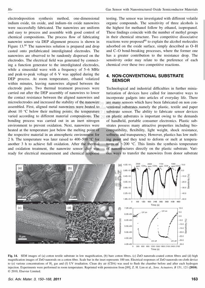
Delivered by Ingenta toInstitute of Molecular and Cell Biology
IP 13713239Tue 19 Jun 2012 003745
REVIEW
Ho Gas Sensor with Nanostructured Oxide Semiconductor Materials
electrodeposition synthesis method one-dimensionalindium oxide tin oxide and indiumndashtin oxide nanowireswere successfully fabricated The nanowires are uniformand easy to process and assemble with good control ofchemical compositions The process flow of fabricatingnanowire sensor via DEP alignment process is shown inFigure 1380 The nanowires solution is prepared and dropcasted onto prefabricated interdigitated electrodes Thenanowires are observed to be randomly dispersed on theelectrodes The electrical field was generated by connect-ing a function generator to the interdigitated electrodeswhile a sinusoidal wave with a frequency of 5ndash6 MHzand peak-to-peak voltage of 6 V was applied during theDEP process At room temperature ethanol volatizedwithin minutes leaving nanowires aligned between theelectrode pairs Two thermal treatment processes werecarried out after the DEP assembly of nanowires to lowerthe contact resistance between the aligned nanowires andmicroelectrodes and increased the stability of the nanowireassembled First aligned metal nanowires were heated toabout 10 C below their melting points the temperaturevaried according to different material compositions Thebonding process was carried out in an inert nitrogenenvironment to prevent oxidation Next nanowires wereheated at the temperature just below the melting point ofthe respective material in an atmospheric environment for2 h The temperature was later raised to 400ndash500 C foranother 3 h to achieve full oxidation After the thermaland oxidation treatment the nanowire sensor chip wasready for electrical measurement and chemical response
ndash500
ndash400
ndash300
ndash200
ndash100
00
100
18E+10
22E+10
26E+10
30E+10
34E+10
38E+10
42E+10
0 600 1200 1800 2400 3000 3600 4200 4800
2500ppmH2
2000ppmH2
1154ppmH2
1000ppmH2
CDA CDA CDACDA
ndash350
ndash300
ndash250
ndash200
ndash150
ndash100
ndash50
00
50
100
40E+09
45E+09
50E+09
55E+09
60E+09
65E+09
70E+09
0 300 600 900 1200 1500 1800 2100 2400 2700
Time (s)
Time (s)
Res
ista
nce
(Ω)
Res
ista
nce
(Ω)
Sen
sitiv
ity (
)
Sen
sitiv
ity (
)
UV onUV on
UV off UV off
(a)
(c) (d)
(b)(e)
(f)
Fig 14 SEM images of (a) cotton textile substrate in low magnification (b) bare cotton fibres (c) ZnO nanorods-coated cotton fibres and (d) highmagnification images of ZnO nanorods on a cotton fibre Scale bar in the inset represents 100 nm Electrical responses of ZnO nanorods-on-cloth deviceto (e) various concentrations of H2 gas and (f) UV irradiation Clean dry air (CDA) was used to flush the chamber before and after each hydrogeninjection Experiments were performed in room temperature Reprinted with permission from [89] Z H Lim et al Sens Actuators B 151 121 (2010)copy 2010 Elsevier Limited
testing The sensor was investigated with different volatileorganic compounds The sensitivity of three alcohols isthe highest for methanol follow by ethanol isopropanolThese findings coincide with the number of methyl groupsin their chemical structure Two competitive dissociativereactions were proposed80 to explain the alcohol moleculesadsorbed on the oxide surface simply described as OndashHand CndashO bond-breaking processes where the former onehas a greater contribution to the resistance drop Thesensitivity order may relate to the preference of eachchemical over these two competitive reactions
4 NON-CONVENTIONAL SUBSTRATESENSOR
Technological and industrial difficulties in further minia-turization of devices have called for innovative ways toincorporate gadgets into articles of everyday life Thereare many sensors which have been fabricated on non con-ventional substrates namely the plastic textile and papersubstrate sensor The ability to fabricate sensor deviceson plastic substrates is important owing to the demandsof handheld portable consumer electronics Plastic sub-strates possess many attractive properties including bio-compatibility flexibility light weight shock resistancesoftness and transparency However plastics has low melt-ing point and they tend to deform or melt at tempera-tures of sim200 C This limits the synthesis temperatureof nanostructures directly on the plastic substrate Vari-ous ways to transfer the nanowires from donor substrate
Sci Adv Mater 3 150ndash168 2011 163
Delivered by Ingenta toInstitute of Molecular and Cell Biology
IP 13713239Tue 19 Jun 2012 003745
REVIEW
Gas Sensor with Nanostructured Oxide Semiconductor Materials Ho
to plastic substrate such as nanoimprint contact transferLangmuir Blogett etc have been developed In additionlow temperature synthesis processes have also been devel-oped to overcome this limitation Mc Alpine et al havereported plastic nanowire sensors based on Si nanowireswhich exhibit parts-per-billion sensitivity to NO2 a haz-ardous pollutant81
Another type of non conventional substrate sensor istextile Clothing is not only a necessity it also encom-passes a complete industry ranging from the down-to-earthbasics to the upmarket and chic Smart clothingtextiles arebecoming very popular in the past decade Smart textileswhich have been developed include silicon flexible skins
(b)
(a)
(d)
(c)
Source-meter
0
2E+09
4E+09
6E+09
8E+09
1E+10
12E+10
14E+10
16E+10
18E+10
I-V 1 I-V 2 I-V 3 I-V 4 I-V 5 Average
Res
ista
nce
(Ω)
Before After
(e)
(f)
(g)
Fig 15 SEM images of (a) low resolution ZnO-nanorods-coated textile with selected area (circled in red) for subsequent studies (b) the selected ZnOnanorods-coated yarns before stretching twisting and sonication (c) the same yarns after repeated stretching and twisting and (d) 5 minutes of watersonification (e) Schematic diagram of the electro-mechanical testing and (f) electrical properties before and after each stretching and twisting cycle(g) Electrical measurement of ZnO nanorods-on-cloth device while subjected to controlled stress cycles with a mechanical testing system Reprintedwith permission from [89] Z H Lim et al Sens Actuators B 151 121 (2010) copy 2010 Elsevier Limited
and organic transistors on textile fibers8283 Another type ofthe smart sensing textiles which uses piezo-resistive prop-erties has been developed The approach for fabricating thefabrics was to coat a thin layer of piezo-resistive materialssuch as polypyrrole or a mixture of rubbers and carbonson conventional fabrics to form fabric-based sensors84ndash86
The function of the developed sensors is similar to that offlexible strain gauges which can measure strains when theyare subjected to a tensile stress Other innovations whichare not actively explored are textiles which can detectenvironmental conditions which then react and adapt toenvironmental changes Furthermore smart textiles can bemade to measure and monitor the physiological conditions
164 Sci Adv Mater 3 150ndash168 2011
Delivered by Ingenta toInstitute of Molecular and Cell Biology
IP 13713239Tue 19 Jun 2012 003745
REVIEW
Ho Gas Sensor with Nanostructured Oxide Semiconductor Materials
of the wearer eg perspiration heartbeat etc Thus they canbe applied various healthcare systems
41 Textile Sensor
While the development of wearable devices has beenreported the incorporation of nano-materials into thedesigns has not been well explored In addition problemssuch as complex process mass production washabilityand wearing comforts needs to be well addressed The easeof synthesizing ZnO nanowires or nanorods on almost anysubstrates welcomes large-scale incorporation on textileZnO nano-structures are believed to be non-toxic and bio-safe87 allowing their direct usage in daily applicationsWhile the use of nano-materials in daily human activitiesraised questions on its potential health risks there is todate no in vivo evidence of toxicity of nano-particulateZnO88
29 nm
5 nm
1 μm1 μm
2 nm 5 μm
15Endash03
16Endash03
17Endash03
18Endash03
Time (s)
on off
1000 ppm
(a)
(c) (d)(f)
(b) (e)
15Endash03
16Endash03
16Endash03
17Endash03
17Endash03
18Endash03
18Endash03
150 250 350 450 550 650 0 150 300 450 600 750 900
Time (s)
Cur
rent
(m
A)
Cur
rent
(m
A)
on off
2000 ppm1500 ppm
1000 ppm2500 ppm
(g) (h)
Fig 16 (andashb) Low and (cndashd) high resolution TEM images of the nanobelts (e) Image of nanobelts sheet made without any addition of binder orreinforcement chemicals (f) Cross-sectional SEM image of the nanobelts sheet Current response of the sensor at (g) varying and (h) same ppm H2
concentration Reprinted with permission from [90] S Bela et al J Phys D Appl Phys 43 35401 (2010) copy 2010 Institute of Physics
SEM images of the textile and nanorods displayed inFigures 14(andashd) show radially oriented nanorods (diametersim80 nm) with hexagonal cross-section grown along thecylindrical fibres (diameter sim15 m)89 Length of thenanorods is sim1 m The nanorods form a uniform anddense coverage around entire lengths of the fibres to forma cross-linked semi-conductive textileThe conductive textile shows excellent multiple sens-
ing (gas and optical) performances at room temperature asshown in Figures 14(e) and (f) respectively In the presenceof hydrogen gas chemisorbed oxygen ions are reducedto release electrons to the conduction band of the ZnOsurface resulting in an increase in conductivity In addi-tion the reduction reaction decreases the surface densityof the oxygen adsorbate leading to a reduction in thewidth of the depletion region and the height of the sur-face potential barrier thus resulting in the decrease in theresistance of the sensor The mechanism for UV sensing
Sci Adv Mater 3 150ndash168 2011 165
Delivered by Ingenta toInstitute of Molecular and Cell Biology
IP 13713239Tue 19 Jun 2012 003745
REVIEW
Gas Sensor with Nanostructured Oxide Semiconductor Materials Ho
is similar to that of hydrogen sensing with holes fromthe photo-generated electronndashhole pairs playing the role ofremoving the adsorbed oxygen molecules insteadA notable feature of the ZnO nanorods-coated textile
device is its fine morphological and electrical stabilityunder multiple stress and washing cycles A critical chal-lenge of semi-conductive yarns and textile is its durabil-ity and constancy of electrical performance SEM analyses(Figs 15(andashd)) of the nanorods -on-cloth before and afterstretching twisting and ashing cycles show no cracks ordelamination of the nanorods from the fibres respectivelyFigure 15(e) shows a schematic of the electro-mechanicaltesting Electrical characterisations made before and aftereach stretching and twisting cycle (Fig 15(f)) show goodelectrical stability We further perform electrical conduc-tivity measurements while stretching and relaxing the tex-tile device in a controlled manner The semiconductingtextile exhibits a higher conductivity when stretched dueto tighter packing (increased contact junctions) of the ZnOnanorods-coated fibers Figure 15(g) shows the variation ofcurrent through the textile device as it underwent repeatedcycles of stress and relaxation When the stress is releasedconductivity falls and stabilises to the original state Againthe morphology of the nanorods-on-textile suffered nocracks of delamination or noticeable degradation after theelectromechanical testing
42 Free Standing Sheet Sensor
Another non conventional sensor substrate is a free stand-ing sheet of nanowire paper The nanostructures are tobe produced in gram quantities so that it can be easilymade into nanostructured paper sheet The thickness ofthe nanostructures sheet can be tuned according to theamount of nanostructures used After the filtering wascompleted a sheet of nanostructures was formed by sand-wiching between a metal calender which was pressed andheated to ensure the nanowires are well dried and bondedtogether to form the free-standing paperBela et al have been reported synthesis of hybrid
titanate and titania nanobelts (Figs 16(andashd)) in a large-scale quantity for gas sensing applications90 The nanobeltsare synthesized from TiO2 powder based on hydrolysis andion exchange of NaOH base and HCl acid respectivelySheets of as-synthesized nanobelts are used for electricaland gas sensing measurements Figure 16(e) shows thewhite nanobelts sheet made without any addition of binderor reinforcement chemicals Cross-sectional SEM image ofFigure 16(f) shows that the nanobelts sheet has a thicknessof sim15 m Figures 16(g and h) show the current responseof the sensor at varying and same ppm H2 concentra-tions respectively The measurements were conducted at anoperating temperature of 300 C From the graphs it is evi-dent that the introduction of hydrogen causes the resistanceof the sensor to reduce because of the injection of electrons
onto the surface of the metal-oxide nanostructures therebyimproving the conductivity of the bulk sensing capabili-ties The resistance increases as the concentration of H2 isvaried from 2500 to 1000 ppm The response time (90of Rair minusRgas is achieved within the first 40ndash50 s whilethe recovery time is 10ndash12 min From the Figure 7(c) itwas observed that the sensing response was rather stableand reversible In oxidizing atmosphere of 300 C ambi-ent oxygen is adsorbed on the surface of nanobelts mostlikely with a negative charge Subsequently with the intro-duction of a reducing H2 gas it reacts with the negativelycharged surface oxygen and decreases the resistance bythe injection of electron
5 CONCLUSIONS
There is an immense technological and scientific potentialsof nanostructured materials in nanodevice applicationsand already numerous nanomaterial based sensors usingvarious materials have been reported These oxide materi-als can be synthesized by various synthetic routes whichinclude both physical and chemical methods The poten-tial application of these nanostructures as sensor dependsgreatly on the ability to precisely control their dimensionchemical composition surface property phase purity andcrystal structure Sensor of various configurations bulktwo-terminal and FET device have been fabricated Theintegrability of the nanostructure sensor into microelec-tronic fabrication technology is an issue that needs tobe addressed Various ways to assemble nanowires so asto ease the device fabrication process have been devel-oped The recent advances in assembling larger and morecomplex nanowire sensor arrays and integrating them intonanoscale electronics can lead to exquisite sensor sys-tem performances These sensory systems can sensitivelytransduce gaschemicalbiological binding events into elec-tronicdigital signals which promise a sophisticated nano-electronics sensing system
6 FUTURE DIRECTIONS
Although nanomaterial based sensors are expected to out-perform their bulk component there are still many issuesand parameters to be studied and addressed Parameters tobe explored include structural and composition tuning aswell as doping and functionalization of surfaces to increaseselectivity sensitivity and materials integrity for long-termstability Other parameters such as limits of detection lim-its of quantification dynamic range response and recov-ery times and lifetime have to be studied and improvedas well The long-term reliability of a sensor is impor-tant since progressive drifts in the characteristics andorresponses of the sensors affect accurate testing and analy-sis The drift of the sensors are frequently related to highworking temperatures and exposure to chemically active
166 Sci Adv Mater 3 150ndash168 2011
Delivered by Ingenta toInstitute of Molecular and Cell Biology
IP 13713239Tue 19 Jun 2012 003745
REVIEW
Ho Gas Sensor with Nanostructured Oxide Semiconductor Materials
ambient gas Many other issues include aging grain-sizegrowth poisoning due to unknown chemical species dif-fusion processes within the device etc are to be addressedas wellThe future direction of the solid-state gas sensor is
towards integrated wirelessremote multi-purpose sens-ing high selectivity recognition of a specific biological orchemical species with ldquoelectronic-nose-tonguerdquo capabili-ties In addition development of miniaturized analyticalsensor which can be integrated in-line orand as standaloneportable sensors is paramount for industrial applicationsThe sensors can further be refined into a network of sensorarrays providing rapid screening monitoring and reportingsystem The data are collected in a database and form partof a feedback guidance system to the control algorithm inindustrial processes
Acknowledgments The work is supported by NationalUniversity of Singapore grant R-263-000-532-112Images used for the cover page are kindly contributed byZ H Lee and M Kevin multidisciplinary laboratory
References and Notes
1 D James S M Scott Z Ali and W T OrsquoHare Microchim Acta149 1 (2005)
2 C-D Kohlin Nanoelectronics and Information Technology editedby R Waser Wiley-VCH Berlin (2005) p 851
3 M E Franke T J Koplin and U Simon Small 2 36 (2006)4 A Kolmakov and M Moskovits Annu Rev Mater Res 34 151
(2004)5 A Mandelis and C Christofides Physics Chemistry and Technology
of Solid State Gas Sensor Devices Wiley-Interscience New York(1993)
6 P T Moseley Sens Actuators B 6 149 (1992)7 N M White and J D Turner Meas Sci Technol 8 1 (1997)8 D Kohl J Phys D 34 R125 (2001)9 N Pinna G Neri M Antonietti and M Niederberger Angew
Chem Int Ed 43 4345 (2004)10 L P Sun L H Huo H Zhao S Gao and J G Zhao Sens Actu-
ators B 114 387 (2006)11 Z F Liu T Yamazaki Y B Shen T Kikuta N Nakatani and
Y X Li Sens Actuators B 129 666 (2008)12 C S Rout A R Raju A Govindaraj and C N R Rao J Nanosci
Nanotechnol 7 1923 (2007)13 M S Arnold P Avouris Z W Pan and Z L Wang J Phys
Chem B 107 659 (2003)14 I Jimenez I M A Centeno R Scotti F Morazzoni A Cornet
and J R Morante J electrochem Soc 150 H72 (2003)15 S Semancik and R E Cavicchi Thin Solid Films 206 81 (1991)16 N S Baik G Sakai N Miura and N Yamazoe Sens Actuators B
63 74 (2000)17 M Ivanovskaya P Bogdanov G Faglia and G Sberveglieri Sens
Actuators B 68 344 (2000)18 K Ihokura and I Watson The Stannic Oxide Gas Sensormdash
Principles and Applications CRC Press Boa Raton (1994)19 K D Schierbaum U Weimar and W Gopel Sens Actuators B
7 1 (1992)20 G Korotcenkov Sens Actuators B 121 664 (2007)21 J G Lu P C Chang and Z Y Fan Mater Sci Eng 52 49 (2006)22 T Yamamoto and H Katayama-Yoshida Jpn J Appl Phys
38 L166 (1999)
23 J G Lu L P Zhu Z Z Ye F Zhuge B H Zhao D W MaL Wang and J Y Huang J Mater Sci 41 467 (2006)
24 J Zhong S Muthukumar Y Chen Y Lu H M Ng W Jiang andE L Garfunkel Appl Phys Lett 83 3401 (2003)
25 S Y Bae C W Na J H Kang and J Park J Phys Chem B109 2526 (2005)
26 S Y Li P Lin C Y Lee T Y Tseng and C J Huang J Phys DAppl Phys 37 2274 (2004)
27 D K Hwang H S Kim J H Lim J Y Oh J H Yang S J ParkK K Kim D C Look and Y S Park Appl Phys Lett 86 151917(2005)
28 W Lee M C Jeong S W Joo and J M Myoung Nanotechnology16 764 (2005)
29 W Lee M C Jeong and J M Myoung Appl Phys Lett 85 6167(2004)
30 D W Zeng C S Xie B L Zhu R Jiang X Chen W L SongJ B Wang and J Shi J Cryst Growth 266 511 (2004)
31 G Z Shen J H Cho J K Yoo G C Yi and C J Lee J PhysChem B 109 5491 (2005)
32 J B Cui and U J Gibson Appl Phys Lett 87 133108 (2005)33 C X Xu X W Sun Z L Dong M B Yu Y Z Xiong and J S
Chen Appl Phys Lett 86 173110 (2005)34 D A Schwartz K R Kittilstved and D R Gamelin Appl Phys
Lett 85 1395 (2004)35 C Ronning P X Gao Y Ding Z L Wang and D Schwen Appl
Phys Lett 84 783 (2004)36 A J Mieszawska R Jalilian G U Sumanasekera and F P
Zamborini Small 3 722 (2007)37 B Zhu K Li S Zhang S Wu and W Huang Prog Chem 20 48
(2008)38 J X Wang S S Xie and W Zhou MRS Bull 32 123 (2007)39 W Lu and C M Lieber J Phys D-Appl Phys 39 R387
(2006)40 X Wang and Y D Li Inorganic Chemistry 45 7522 (2006)41 Y Shen T Yamazaki Z Liu D Meng T Kikuta N Nakatani
M Saito and M Mori Sens Actuators B 135 524 (2009)42 A Kolmakov Y Zhang G Cheng and M Moskovits Adv Mater
15 997 (2003)43 X T Zhou J Q Hu C P Li D D D Ma C S Lee and S T
Lee Chem Phys Lett 369 220 (2003)44 T-J Hsueh C-L Hsu S-J Chang and I-C Chen Sens Actua-
tors B 126 473 (2007)45 Q Wan Q H Li Y J Chen T H Wang X L He J P Li and
C L Lin Appl Phys Lett 84 3654 (2004)46 G J Li X H Zhang and S Kawi Sens Actuators B 60 64 (1999)47 G J Li and S Kawi Talanta 45 759 (1998)48 E T H Tan G W Ho A S W Wong S Kawi and A T S Wee
Nanotechnology 19 255706 (2008)49 S Luo G Fu H Chen and Y Zhang Mater Chem Phys 109 541
(2008)50 C Y Wang M Ali T Kups C C Roehlig V Cimalla T Stauden
and O Ambacher Sens Actuators B 130 589 (2008)51 J Ahmed S Vaidya T Ahmad P Sujatha Devi D Das and A K
Ashok Mater Res Bull 43 264 (2008)52 J Kaur R Kumar and M C Bhatnagar Sens Actuators B
126 478 (2007)53 D Lutic M Strand A Lloyd-Spetz K Buchholt E Ieva P O
Kall and M Sanati Top Cata 45 105 (2007)54 A Teleki S E Pratsinis K Kalyanasundaram and P I Gouma
Sens Actuators B 119 683 (2006)55 X L Gou G X Wang X Y Kong D Wexler J Horvat J Yang
and J Park Chem Eur J 14 5996 (2008)56 X Feng Z J Li P Y Wang and Y F Zhou J Mat Sci 40 6597
(2005)57 J Chen L Xu W Li and X Gou Adv Mater 17 582 (2005)58 Z B Zhuang Q Peng J F Liu X Wang and Y D Li Inorg
Chem 46 5179 (2007)
Sci Adv Mater 3 150ndash168 2011 167
Delivered by Ingenta toInstitute of Molecular and Cell Biology
IP 13713239Tue 19 Jun 2012 003745
REVIEW
Gas Sensor with Nanostructured Oxide Semiconductor Materials Ho
59 M-W Ahn K-S Park J-H Heo D-W Kim K J Choi and J-GPark Sens Actuators B 138 168 (2009)
60 H T Wang B S Kang F Ren L C Tien P W Sadik D PNorton S J Pearton and J Lin Appl Phys A 81 1117 (2005)
61 B Wang L F Zhu Y H Yang N S Xu and G W Yang J PhysChem C 112 6643 (2008)
62 T H Jung S-I Kwon J-H Park D-G Lim Y-J Choi and J-GPark Appl Phys A 91 707 (2008)
63 S C Yeow W L Ong A S W Wong and G W Ho Sens Actu-ators B 143 295 (2009)
64 V V Sysoeva T Schneiderb J Goschnickb I KiselevbW Habichtb H Hahnb E Strelcovc and A Kolmakov Sens Actu-ators B 139 699 (2009)
65 Y B Shen T Yamazaki Z F Liu D Meng T Kikuta N NakataniM Saito and M Mori Sens Actuators B 135 524 (2009)
66 Y Huang S Yue Z Wang Q Wang C Shi Z Xu X D BaiC Tang and C Gu J Phys Chem B 110 796 (2006)
67 R Khan H-W Ra J T Kim W S Jang D Sharma and Y HIm Sens Actuators B 150 389 (2010)
68 C Li D H Zhang X L Liu S Han T Tang J Han and C ZhouAppl Phys Lett 82 1613 (2003)
69 Z Fan and J G Lu Appl Phys Lett 86 123510 (2005)70 Z Y Fan D W Wang P C Chang W Y Tseng and J G Lu
Appl Phys Lett 85 5923 (2004)71 M Liess Thin Solid Films 410 183 (2002)72 D H Zhang Z Q Liu C Li T Tang X L Liu S Han B Lei
and C W Zhou Nano Lett 4 1919 (2004)73 A Kolmakov D O Klenov Y Lilach S Stemmer and
M Moskovits Nano Lett 5 667 (2005)74 A Javey S W Nam R S Friedman H Yan and C M Lieber
Nano Lett 7 773 (2007)75 Y G Sun and J A Rogers Nano Lett 4 1953 (2004)
76 Z Fan J C Ho Z A Jacobson R Yerushalmi R L AlleyH Razavi and A Javey Nano Lett 8 20 (2008)
77 Z Y Fan J C Ho T Takahashi R Yerushalmi K Takei A CFord Y-L Chueh and A Javey Adv Mater 21 3730 (2009)
78 K W Jiang W J Liu L J Wan and J Zhang Sens Actuators B134 79 (2008)
79 X P Li E China H W Sun P Kurup and Z Y Gu Sens Actu-ators B 148 404 (2010)
80 T Jinkawa G Sakai J Tamaki N Miura and N Yamazoe J MolCatal A 155 193 (2000)
81 M C McAlpine H Ahmad D W Wang and J R Heath NatMater 6 379 (2007)
82 R B Katragadda and Y Xu A Novel Intelligent Textile TechnologyBased on Silicon Flexible Skins Electrical and Computer Engineer-ing Wayne State University Detroit Michigan USA ISWC (2005)pp 78ndash81
83 J B Lee and V Subramanian IEEE Trans Electron Devices 62 269(2005)
84 R Wijesiriwardana K Mitcham and T Dias Fibre-meshed trans-ducers based real time wearable physiological information moni-toring system Proceedings of the 8th International Symposium onWearable Computers ISWCrsquo04 (2004) pp 40ndash47
85 R Wijesiriwardana IEEE Sens J 6 571 (2006)86 E P Scilingo F Lorussi A Mazzoldi and D De Rossi Sens J
IEEE 3 460 (2003)87 J Zhou N Xu and Z L Wang Adv Mater 18 2432 (2006)88 G J Nohynek E K Dudour and M S Roberts Nanotechnology
21 136 (2008)89 Z H Lim Z X Chia M Kevin A S W Wong and G W Ho
Sens Actuators B 151 121 (2010)90 S Bela A S W Wong and G W Ho J Phys D Appl Phys
43 35401 (2010)
Received 4 November 2010 Accepted 20 January 2011
168 Sci Adv Mater 3 150ndash168 2011

Delivered by Ingenta toInstitute of Molecular and Cell Biology
IP 13713239Tue 19 Jun 2012 003745
REVIEW
Gas Sensor with Nanostructured Oxide Semiconductor Materials Ho
to plastic substrate such as nanoimprint contact transferLangmuir Blogett etc have been developed In additionlow temperature synthesis processes have also been devel-oped to overcome this limitation Mc Alpine et al havereported plastic nanowire sensors based on Si nanowireswhich exhibit parts-per-billion sensitivity to NO2 a haz-ardous pollutant81
Another type of non conventional substrate sensor istextile Clothing is not only a necessity it also encom-passes a complete industry ranging from the down-to-earthbasics to the upmarket and chic Smart clothingtextiles arebecoming very popular in the past decade Smart textileswhich have been developed include silicon flexible skins
(b)
(a)
(d)
(c)
Source-meter
0
2E+09
4E+09
6E+09
8E+09
1E+10
12E+10
14E+10
16E+10
18E+10
I-V 1 I-V 2 I-V 3 I-V 4 I-V 5 Average
Res
ista
nce
(Ω)
Before After
(e)
(f)
(g)
Fig 15 SEM images of (a) low resolution ZnO-nanorods-coated textile with selected area (circled in red) for subsequent studies (b) the selected ZnOnanorods-coated yarns before stretching twisting and sonication (c) the same yarns after repeated stretching and twisting and (d) 5 minutes of watersonification (e) Schematic diagram of the electro-mechanical testing and (f) electrical properties before and after each stretching and twisting cycle(g) Electrical measurement of ZnO nanorods-on-cloth device while subjected to controlled stress cycles with a mechanical testing system Reprintedwith permission from [89] Z H Lim et al Sens Actuators B 151 121 (2010) copy 2010 Elsevier Limited
and organic transistors on textile fibers8283 Another type ofthe smart sensing textiles which uses piezo-resistive prop-erties has been developed The approach for fabricating thefabrics was to coat a thin layer of piezo-resistive materialssuch as polypyrrole or a mixture of rubbers and carbonson conventional fabrics to form fabric-based sensors84ndash86
The function of the developed sensors is similar to that offlexible strain gauges which can measure strains when theyare subjected to a tensile stress Other innovations whichare not actively explored are textiles which can detectenvironmental conditions which then react and adapt toenvironmental changes Furthermore smart textiles can bemade to measure and monitor the physiological conditions
164 Sci Adv Mater 3 150ndash168 2011
Delivered by Ingenta toInstitute of Molecular and Cell Biology
IP 13713239Tue 19 Jun 2012 003745
REVIEW
Ho Gas Sensor with Nanostructured Oxide Semiconductor Materials
of the wearer eg perspiration heartbeat etc Thus they canbe applied various healthcare systems
41 Textile Sensor
While the development of wearable devices has beenreported the incorporation of nano-materials into thedesigns has not been well explored In addition problemssuch as complex process mass production washabilityand wearing comforts needs to be well addressed The easeof synthesizing ZnO nanowires or nanorods on almost anysubstrates welcomes large-scale incorporation on textileZnO nano-structures are believed to be non-toxic and bio-safe87 allowing their direct usage in daily applicationsWhile the use of nano-materials in daily human activitiesraised questions on its potential health risks there is todate no in vivo evidence of toxicity of nano-particulateZnO88
29 nm
5 nm
1 μm1 μm
2 nm 5 μm
15Endash03
16Endash03
17Endash03
18Endash03
Time (s)
on off
1000 ppm
(a)
(c) (d)(f)
(b) (e)
15Endash03
16Endash03
16Endash03
17Endash03
17Endash03
18Endash03
18Endash03
150 250 350 450 550 650 0 150 300 450 600 750 900
Time (s)
Cur
rent
(m
A)
Cur
rent
(m
A)
on off
2000 ppm1500 ppm
1000 ppm2500 ppm
(g) (h)
Fig 16 (andashb) Low and (cndashd) high resolution TEM images of the nanobelts (e) Image of nanobelts sheet made without any addition of binder orreinforcement chemicals (f) Cross-sectional SEM image of the nanobelts sheet Current response of the sensor at (g) varying and (h) same ppm H2
concentration Reprinted with permission from [90] S Bela et al J Phys D Appl Phys 43 35401 (2010) copy 2010 Institute of Physics
SEM images of the textile and nanorods displayed inFigures 14(andashd) show radially oriented nanorods (diametersim80 nm) with hexagonal cross-section grown along thecylindrical fibres (diameter sim15 m)89 Length of thenanorods is sim1 m The nanorods form a uniform anddense coverage around entire lengths of the fibres to forma cross-linked semi-conductive textileThe conductive textile shows excellent multiple sens-
ing (gas and optical) performances at room temperature asshown in Figures 14(e) and (f) respectively In the presenceof hydrogen gas chemisorbed oxygen ions are reducedto release electrons to the conduction band of the ZnOsurface resulting in an increase in conductivity In addi-tion the reduction reaction decreases the surface densityof the oxygen adsorbate leading to a reduction in thewidth of the depletion region and the height of the sur-face potential barrier thus resulting in the decrease in theresistance of the sensor The mechanism for UV sensing
Sci Adv Mater 3 150ndash168 2011 165
Delivered by Ingenta toInstitute of Molecular and Cell Biology
IP 13713239Tue 19 Jun 2012 003745
REVIEW
Gas Sensor with Nanostructured Oxide Semiconductor Materials Ho
is similar to that of hydrogen sensing with holes fromthe photo-generated electronndashhole pairs playing the role ofremoving the adsorbed oxygen molecules insteadA notable feature of the ZnO nanorods-coated textile
device is its fine morphological and electrical stabilityunder multiple stress and washing cycles A critical chal-lenge of semi-conductive yarns and textile is its durabil-ity and constancy of electrical performance SEM analyses(Figs 15(andashd)) of the nanorods -on-cloth before and afterstretching twisting and ashing cycles show no cracks ordelamination of the nanorods from the fibres respectivelyFigure 15(e) shows a schematic of the electro-mechanicaltesting Electrical characterisations made before and aftereach stretching and twisting cycle (Fig 15(f)) show goodelectrical stability We further perform electrical conduc-tivity measurements while stretching and relaxing the tex-tile device in a controlled manner The semiconductingtextile exhibits a higher conductivity when stretched dueto tighter packing (increased contact junctions) of the ZnOnanorods-coated fibers Figure 15(g) shows the variation ofcurrent through the textile device as it underwent repeatedcycles of stress and relaxation When the stress is releasedconductivity falls and stabilises to the original state Againthe morphology of the nanorods-on-textile suffered nocracks of delamination or noticeable degradation after theelectromechanical testing
42 Free Standing Sheet Sensor
Another non conventional sensor substrate is a free stand-ing sheet of nanowire paper The nanostructures are tobe produced in gram quantities so that it can be easilymade into nanostructured paper sheet The thickness ofthe nanostructures sheet can be tuned according to theamount of nanostructures used After the filtering wascompleted a sheet of nanostructures was formed by sand-wiching between a metal calender which was pressed andheated to ensure the nanowires are well dried and bondedtogether to form the free-standing paperBela et al have been reported synthesis of hybrid
titanate and titania nanobelts (Figs 16(andashd)) in a large-scale quantity for gas sensing applications90 The nanobeltsare synthesized from TiO2 powder based on hydrolysis andion exchange of NaOH base and HCl acid respectivelySheets of as-synthesized nanobelts are used for electricaland gas sensing measurements Figure 16(e) shows thewhite nanobelts sheet made without any addition of binderor reinforcement chemicals Cross-sectional SEM image ofFigure 16(f) shows that the nanobelts sheet has a thicknessof sim15 m Figures 16(g and h) show the current responseof the sensor at varying and same ppm H2 concentra-tions respectively The measurements were conducted at anoperating temperature of 300 C From the graphs it is evi-dent that the introduction of hydrogen causes the resistanceof the sensor to reduce because of the injection of electrons
onto the surface of the metal-oxide nanostructures therebyimproving the conductivity of the bulk sensing capabili-ties The resistance increases as the concentration of H2 isvaried from 2500 to 1000 ppm The response time (90of Rair minusRgas is achieved within the first 40ndash50 s whilethe recovery time is 10ndash12 min From the Figure 7(c) itwas observed that the sensing response was rather stableand reversible In oxidizing atmosphere of 300 C ambi-ent oxygen is adsorbed on the surface of nanobelts mostlikely with a negative charge Subsequently with the intro-duction of a reducing H2 gas it reacts with the negativelycharged surface oxygen and decreases the resistance bythe injection of electron
5 CONCLUSIONS
There is an immense technological and scientific potentialsof nanostructured materials in nanodevice applicationsand already numerous nanomaterial based sensors usingvarious materials have been reported These oxide materi-als can be synthesized by various synthetic routes whichinclude both physical and chemical methods The poten-tial application of these nanostructures as sensor dependsgreatly on the ability to precisely control their dimensionchemical composition surface property phase purity andcrystal structure Sensor of various configurations bulktwo-terminal and FET device have been fabricated Theintegrability of the nanostructure sensor into microelec-tronic fabrication technology is an issue that needs tobe addressed Various ways to assemble nanowires so asto ease the device fabrication process have been devel-oped The recent advances in assembling larger and morecomplex nanowire sensor arrays and integrating them intonanoscale electronics can lead to exquisite sensor sys-tem performances These sensory systems can sensitivelytransduce gaschemicalbiological binding events into elec-tronicdigital signals which promise a sophisticated nano-electronics sensing system
6 FUTURE DIRECTIONS
Although nanomaterial based sensors are expected to out-perform their bulk component there are still many issuesand parameters to be studied and addressed Parameters tobe explored include structural and composition tuning aswell as doping and functionalization of surfaces to increaseselectivity sensitivity and materials integrity for long-termstability Other parameters such as limits of detection lim-its of quantification dynamic range response and recov-ery times and lifetime have to be studied and improvedas well The long-term reliability of a sensor is impor-tant since progressive drifts in the characteristics andorresponses of the sensors affect accurate testing and analy-sis The drift of the sensors are frequently related to highworking temperatures and exposure to chemically active
166 Sci Adv Mater 3 150ndash168 2011
Delivered by Ingenta toInstitute of Molecular and Cell Biology
IP 13713239Tue 19 Jun 2012 003745
REVIEW
Ho Gas Sensor with Nanostructured Oxide Semiconductor Materials
ambient gas Many other issues include aging grain-sizegrowth poisoning due to unknown chemical species dif-fusion processes within the device etc are to be addressedas wellThe future direction of the solid-state gas sensor is
towards integrated wirelessremote multi-purpose sens-ing high selectivity recognition of a specific biological orchemical species with ldquoelectronic-nose-tonguerdquo capabili-ties In addition development of miniaturized analyticalsensor which can be integrated in-line orand as standaloneportable sensors is paramount for industrial applicationsThe sensors can further be refined into a network of sensorarrays providing rapid screening monitoring and reportingsystem The data are collected in a database and form partof a feedback guidance system to the control algorithm inindustrial processes
Acknowledgments The work is supported by NationalUniversity of Singapore grant R-263-000-532-112Images used for the cover page are kindly contributed byZ H Lee and M Kevin multidisciplinary laboratory
References and Notes
1 D James S M Scott Z Ali and W T OrsquoHare Microchim Acta149 1 (2005)
2 C-D Kohlin Nanoelectronics and Information Technology editedby R Waser Wiley-VCH Berlin (2005) p 851
3 M E Franke T J Koplin and U Simon Small 2 36 (2006)4 A Kolmakov and M Moskovits Annu Rev Mater Res 34 151
(2004)5 A Mandelis and C Christofides Physics Chemistry and Technology
of Solid State Gas Sensor Devices Wiley-Interscience New York(1993)
6 P T Moseley Sens Actuators B 6 149 (1992)7 N M White and J D Turner Meas Sci Technol 8 1 (1997)8 D Kohl J Phys D 34 R125 (2001)9 N Pinna G Neri M Antonietti and M Niederberger Angew
Chem Int Ed 43 4345 (2004)10 L P Sun L H Huo H Zhao S Gao and J G Zhao Sens Actu-
ators B 114 387 (2006)11 Z F Liu T Yamazaki Y B Shen T Kikuta N Nakatani and
Y X Li Sens Actuators B 129 666 (2008)12 C S Rout A R Raju A Govindaraj and C N R Rao J Nanosci
Nanotechnol 7 1923 (2007)13 M S Arnold P Avouris Z W Pan and Z L Wang J Phys
Chem B 107 659 (2003)14 I Jimenez I M A Centeno R Scotti F Morazzoni A Cornet
and J R Morante J electrochem Soc 150 H72 (2003)15 S Semancik and R E Cavicchi Thin Solid Films 206 81 (1991)16 N S Baik G Sakai N Miura and N Yamazoe Sens Actuators B
63 74 (2000)17 M Ivanovskaya P Bogdanov G Faglia and G Sberveglieri Sens
Actuators B 68 344 (2000)18 K Ihokura and I Watson The Stannic Oxide Gas Sensormdash
Principles and Applications CRC Press Boa Raton (1994)19 K D Schierbaum U Weimar and W Gopel Sens Actuators B
7 1 (1992)20 G Korotcenkov Sens Actuators B 121 664 (2007)21 J G Lu P C Chang and Z Y Fan Mater Sci Eng 52 49 (2006)22 T Yamamoto and H Katayama-Yoshida Jpn J Appl Phys
38 L166 (1999)
23 J G Lu L P Zhu Z Z Ye F Zhuge B H Zhao D W MaL Wang and J Y Huang J Mater Sci 41 467 (2006)
24 J Zhong S Muthukumar Y Chen Y Lu H M Ng W Jiang andE L Garfunkel Appl Phys Lett 83 3401 (2003)
25 S Y Bae C W Na J H Kang and J Park J Phys Chem B109 2526 (2005)
26 S Y Li P Lin C Y Lee T Y Tseng and C J Huang J Phys DAppl Phys 37 2274 (2004)
27 D K Hwang H S Kim J H Lim J Y Oh J H Yang S J ParkK K Kim D C Look and Y S Park Appl Phys Lett 86 151917(2005)
28 W Lee M C Jeong S W Joo and J M Myoung Nanotechnology16 764 (2005)
29 W Lee M C Jeong and J M Myoung Appl Phys Lett 85 6167(2004)
30 D W Zeng C S Xie B L Zhu R Jiang X Chen W L SongJ B Wang and J Shi J Cryst Growth 266 511 (2004)
31 G Z Shen J H Cho J K Yoo G C Yi and C J Lee J PhysChem B 109 5491 (2005)
32 J B Cui and U J Gibson Appl Phys Lett 87 133108 (2005)33 C X Xu X W Sun Z L Dong M B Yu Y Z Xiong and J S
Chen Appl Phys Lett 86 173110 (2005)34 D A Schwartz K R Kittilstved and D R Gamelin Appl Phys
Lett 85 1395 (2004)35 C Ronning P X Gao Y Ding Z L Wang and D Schwen Appl
Phys Lett 84 783 (2004)36 A J Mieszawska R Jalilian G U Sumanasekera and F P
Zamborini Small 3 722 (2007)37 B Zhu K Li S Zhang S Wu and W Huang Prog Chem 20 48
(2008)38 J X Wang S S Xie and W Zhou MRS Bull 32 123 (2007)39 W Lu and C M Lieber J Phys D-Appl Phys 39 R387
(2006)40 X Wang and Y D Li Inorganic Chemistry 45 7522 (2006)41 Y Shen T Yamazaki Z Liu D Meng T Kikuta N Nakatani
M Saito and M Mori Sens Actuators B 135 524 (2009)42 A Kolmakov Y Zhang G Cheng and M Moskovits Adv Mater
15 997 (2003)43 X T Zhou J Q Hu C P Li D D D Ma C S Lee and S T
Lee Chem Phys Lett 369 220 (2003)44 T-J Hsueh C-L Hsu S-J Chang and I-C Chen Sens Actua-
tors B 126 473 (2007)45 Q Wan Q H Li Y J Chen T H Wang X L He J P Li and
C L Lin Appl Phys Lett 84 3654 (2004)46 G J Li X H Zhang and S Kawi Sens Actuators B 60 64 (1999)47 G J Li and S Kawi Talanta 45 759 (1998)48 E T H Tan G W Ho A S W Wong S Kawi and A T S Wee
Nanotechnology 19 255706 (2008)49 S Luo G Fu H Chen and Y Zhang Mater Chem Phys 109 541
(2008)50 C Y Wang M Ali T Kups C C Roehlig V Cimalla T Stauden
and O Ambacher Sens Actuators B 130 589 (2008)51 J Ahmed S Vaidya T Ahmad P Sujatha Devi D Das and A K
Ashok Mater Res Bull 43 264 (2008)52 J Kaur R Kumar and M C Bhatnagar Sens Actuators B
126 478 (2007)53 D Lutic M Strand A Lloyd-Spetz K Buchholt E Ieva P O
Kall and M Sanati Top Cata 45 105 (2007)54 A Teleki S E Pratsinis K Kalyanasundaram and P I Gouma
Sens Actuators B 119 683 (2006)55 X L Gou G X Wang X Y Kong D Wexler J Horvat J Yang
and J Park Chem Eur J 14 5996 (2008)56 X Feng Z J Li P Y Wang and Y F Zhou J Mat Sci 40 6597
(2005)57 J Chen L Xu W Li and X Gou Adv Mater 17 582 (2005)58 Z B Zhuang Q Peng J F Liu X Wang and Y D Li Inorg
Chem 46 5179 (2007)
Sci Adv Mater 3 150ndash168 2011 167
Delivered by Ingenta toInstitute of Molecular and Cell Biology
IP 13713239Tue 19 Jun 2012 003745
REVIEW
Gas Sensor with Nanostructured Oxide Semiconductor Materials Ho
59 M-W Ahn K-S Park J-H Heo D-W Kim K J Choi and J-GPark Sens Actuators B 138 168 (2009)
60 H T Wang B S Kang F Ren L C Tien P W Sadik D PNorton S J Pearton and J Lin Appl Phys A 81 1117 (2005)
61 B Wang L F Zhu Y H Yang N S Xu and G W Yang J PhysChem C 112 6643 (2008)
62 T H Jung S-I Kwon J-H Park D-G Lim Y-J Choi and J-GPark Appl Phys A 91 707 (2008)
63 S C Yeow W L Ong A S W Wong and G W Ho Sens Actu-ators B 143 295 (2009)
64 V V Sysoeva T Schneiderb J Goschnickb I KiselevbW Habichtb H Hahnb E Strelcovc and A Kolmakov Sens Actu-ators B 139 699 (2009)
65 Y B Shen T Yamazaki Z F Liu D Meng T Kikuta N NakataniM Saito and M Mori Sens Actuators B 135 524 (2009)
66 Y Huang S Yue Z Wang Q Wang C Shi Z Xu X D BaiC Tang and C Gu J Phys Chem B 110 796 (2006)
67 R Khan H-W Ra J T Kim W S Jang D Sharma and Y HIm Sens Actuators B 150 389 (2010)
68 C Li D H Zhang X L Liu S Han T Tang J Han and C ZhouAppl Phys Lett 82 1613 (2003)
69 Z Fan and J G Lu Appl Phys Lett 86 123510 (2005)70 Z Y Fan D W Wang P C Chang W Y Tseng and J G Lu
Appl Phys Lett 85 5923 (2004)71 M Liess Thin Solid Films 410 183 (2002)72 D H Zhang Z Q Liu C Li T Tang X L Liu S Han B Lei
and C W Zhou Nano Lett 4 1919 (2004)73 A Kolmakov D O Klenov Y Lilach S Stemmer and
M Moskovits Nano Lett 5 667 (2005)74 A Javey S W Nam R S Friedman H Yan and C M Lieber
Nano Lett 7 773 (2007)75 Y G Sun and J A Rogers Nano Lett 4 1953 (2004)
76 Z Fan J C Ho Z A Jacobson R Yerushalmi R L AlleyH Razavi and A Javey Nano Lett 8 20 (2008)
77 Z Y Fan J C Ho T Takahashi R Yerushalmi K Takei A CFord Y-L Chueh and A Javey Adv Mater 21 3730 (2009)
78 K W Jiang W J Liu L J Wan and J Zhang Sens Actuators B134 79 (2008)
79 X P Li E China H W Sun P Kurup and Z Y Gu Sens Actu-ators B 148 404 (2010)
80 T Jinkawa G Sakai J Tamaki N Miura and N Yamazoe J MolCatal A 155 193 (2000)
81 M C McAlpine H Ahmad D W Wang and J R Heath NatMater 6 379 (2007)
82 R B Katragadda and Y Xu A Novel Intelligent Textile TechnologyBased on Silicon Flexible Skins Electrical and Computer Engineer-ing Wayne State University Detroit Michigan USA ISWC (2005)pp 78ndash81
83 J B Lee and V Subramanian IEEE Trans Electron Devices 62 269(2005)
84 R Wijesiriwardana K Mitcham and T Dias Fibre-meshed trans-ducers based real time wearable physiological information moni-toring system Proceedings of the 8th International Symposium onWearable Computers ISWCrsquo04 (2004) pp 40ndash47
85 R Wijesiriwardana IEEE Sens J 6 571 (2006)86 E P Scilingo F Lorussi A Mazzoldi and D De Rossi Sens J
IEEE 3 460 (2003)87 J Zhou N Xu and Z L Wang Adv Mater 18 2432 (2006)88 G J Nohynek E K Dudour and M S Roberts Nanotechnology
21 136 (2008)89 Z H Lim Z X Chia M Kevin A S W Wong and G W Ho
Sens Actuators B 151 121 (2010)90 S Bela A S W Wong and G W Ho J Phys D Appl Phys
43 35401 (2010)
Received 4 November 2010 Accepted 20 January 2011
168 Sci Adv Mater 3 150ndash168 2011
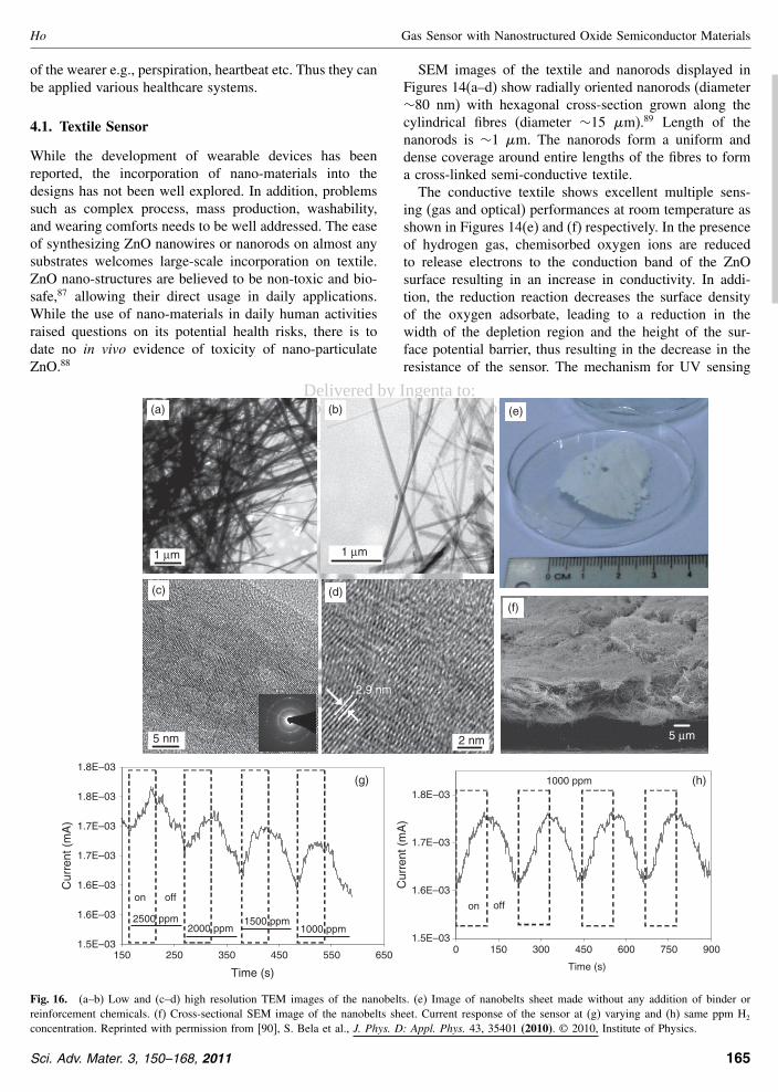
Delivered by Ingenta toInstitute of Molecular and Cell Biology
IP 13713239Tue 19 Jun 2012 003745
REVIEW
Ho Gas Sensor with Nanostructured Oxide Semiconductor Materials
of the wearer eg perspiration heartbeat etc Thus they canbe applied various healthcare systems
41 Textile Sensor
While the development of wearable devices has beenreported the incorporation of nano-materials into thedesigns has not been well explored In addition problemssuch as complex process mass production washabilityand wearing comforts needs to be well addressed The easeof synthesizing ZnO nanowires or nanorods on almost anysubstrates welcomes large-scale incorporation on textileZnO nano-structures are believed to be non-toxic and bio-safe87 allowing their direct usage in daily applicationsWhile the use of nano-materials in daily human activitiesraised questions on its potential health risks there is todate no in vivo evidence of toxicity of nano-particulateZnO88
29 nm
5 nm
1 μm1 μm
2 nm 5 μm
15Endash03
16Endash03
17Endash03
18Endash03
Time (s)
on off
1000 ppm
(a)
(c) (d)(f)
(b) (e)
15Endash03
16Endash03
16Endash03
17Endash03
17Endash03
18Endash03
18Endash03
150 250 350 450 550 650 0 150 300 450 600 750 900
Time (s)
Cur
rent
(m
A)
Cur
rent
(m
A)
on off
2000 ppm1500 ppm
1000 ppm2500 ppm
(g) (h)
Fig 16 (andashb) Low and (cndashd) high resolution TEM images of the nanobelts (e) Image of nanobelts sheet made without any addition of binder orreinforcement chemicals (f) Cross-sectional SEM image of the nanobelts sheet Current response of the sensor at (g) varying and (h) same ppm H2
concentration Reprinted with permission from [90] S Bela et al J Phys D Appl Phys 43 35401 (2010) copy 2010 Institute of Physics
SEM images of the textile and nanorods displayed inFigures 14(andashd) show radially oriented nanorods (diametersim80 nm) with hexagonal cross-section grown along thecylindrical fibres (diameter sim15 m)89 Length of thenanorods is sim1 m The nanorods form a uniform anddense coverage around entire lengths of the fibres to forma cross-linked semi-conductive textileThe conductive textile shows excellent multiple sens-
ing (gas and optical) performances at room temperature asshown in Figures 14(e) and (f) respectively In the presenceof hydrogen gas chemisorbed oxygen ions are reducedto release electrons to the conduction band of the ZnOsurface resulting in an increase in conductivity In addi-tion the reduction reaction decreases the surface densityof the oxygen adsorbate leading to a reduction in thewidth of the depletion region and the height of the sur-face potential barrier thus resulting in the decrease in theresistance of the sensor The mechanism for UV sensing
Sci Adv Mater 3 150ndash168 2011 165
Delivered by Ingenta toInstitute of Molecular and Cell Biology
IP 13713239Tue 19 Jun 2012 003745
REVIEW
Gas Sensor with Nanostructured Oxide Semiconductor Materials Ho
is similar to that of hydrogen sensing with holes fromthe photo-generated electronndashhole pairs playing the role ofremoving the adsorbed oxygen molecules insteadA notable feature of the ZnO nanorods-coated textile
device is its fine morphological and electrical stabilityunder multiple stress and washing cycles A critical chal-lenge of semi-conductive yarns and textile is its durabil-ity and constancy of electrical performance SEM analyses(Figs 15(andashd)) of the nanorods -on-cloth before and afterstretching twisting and ashing cycles show no cracks ordelamination of the nanorods from the fibres respectivelyFigure 15(e) shows a schematic of the electro-mechanicaltesting Electrical characterisations made before and aftereach stretching and twisting cycle (Fig 15(f)) show goodelectrical stability We further perform electrical conduc-tivity measurements while stretching and relaxing the tex-tile device in a controlled manner The semiconductingtextile exhibits a higher conductivity when stretched dueto tighter packing (increased contact junctions) of the ZnOnanorods-coated fibers Figure 15(g) shows the variation ofcurrent through the textile device as it underwent repeatedcycles of stress and relaxation When the stress is releasedconductivity falls and stabilises to the original state Againthe morphology of the nanorods-on-textile suffered nocracks of delamination or noticeable degradation after theelectromechanical testing
42 Free Standing Sheet Sensor
Another non conventional sensor substrate is a free stand-ing sheet of nanowire paper The nanostructures are tobe produced in gram quantities so that it can be easilymade into nanostructured paper sheet The thickness ofthe nanostructures sheet can be tuned according to theamount of nanostructures used After the filtering wascompleted a sheet of nanostructures was formed by sand-wiching between a metal calender which was pressed andheated to ensure the nanowires are well dried and bondedtogether to form the free-standing paperBela et al have been reported synthesis of hybrid
titanate and titania nanobelts (Figs 16(andashd)) in a large-scale quantity for gas sensing applications90 The nanobeltsare synthesized from TiO2 powder based on hydrolysis andion exchange of NaOH base and HCl acid respectivelySheets of as-synthesized nanobelts are used for electricaland gas sensing measurements Figure 16(e) shows thewhite nanobelts sheet made without any addition of binderor reinforcement chemicals Cross-sectional SEM image ofFigure 16(f) shows that the nanobelts sheet has a thicknessof sim15 m Figures 16(g and h) show the current responseof the sensor at varying and same ppm H2 concentra-tions respectively The measurements were conducted at anoperating temperature of 300 C From the graphs it is evi-dent that the introduction of hydrogen causes the resistanceof the sensor to reduce because of the injection of electrons
onto the surface of the metal-oxide nanostructures therebyimproving the conductivity of the bulk sensing capabili-ties The resistance increases as the concentration of H2 isvaried from 2500 to 1000 ppm The response time (90of Rair minusRgas is achieved within the first 40ndash50 s whilethe recovery time is 10ndash12 min From the Figure 7(c) itwas observed that the sensing response was rather stableand reversible In oxidizing atmosphere of 300 C ambi-ent oxygen is adsorbed on the surface of nanobelts mostlikely with a negative charge Subsequently with the intro-duction of a reducing H2 gas it reacts with the negativelycharged surface oxygen and decreases the resistance bythe injection of electron
5 CONCLUSIONS
There is an immense technological and scientific potentialsof nanostructured materials in nanodevice applicationsand already numerous nanomaterial based sensors usingvarious materials have been reported These oxide materi-als can be synthesized by various synthetic routes whichinclude both physical and chemical methods The poten-tial application of these nanostructures as sensor dependsgreatly on the ability to precisely control their dimensionchemical composition surface property phase purity andcrystal structure Sensor of various configurations bulktwo-terminal and FET device have been fabricated Theintegrability of the nanostructure sensor into microelec-tronic fabrication technology is an issue that needs tobe addressed Various ways to assemble nanowires so asto ease the device fabrication process have been devel-oped The recent advances in assembling larger and morecomplex nanowire sensor arrays and integrating them intonanoscale electronics can lead to exquisite sensor sys-tem performances These sensory systems can sensitivelytransduce gaschemicalbiological binding events into elec-tronicdigital signals which promise a sophisticated nano-electronics sensing system
6 FUTURE DIRECTIONS
Although nanomaterial based sensors are expected to out-perform their bulk component there are still many issuesand parameters to be studied and addressed Parameters tobe explored include structural and composition tuning aswell as doping and functionalization of surfaces to increaseselectivity sensitivity and materials integrity for long-termstability Other parameters such as limits of detection lim-its of quantification dynamic range response and recov-ery times and lifetime have to be studied and improvedas well The long-term reliability of a sensor is impor-tant since progressive drifts in the characteristics andorresponses of the sensors affect accurate testing and analy-sis The drift of the sensors are frequently related to highworking temperatures and exposure to chemically active
166 Sci Adv Mater 3 150ndash168 2011
Delivered by Ingenta toInstitute of Molecular and Cell Biology
IP 13713239Tue 19 Jun 2012 003745
REVIEW
Ho Gas Sensor with Nanostructured Oxide Semiconductor Materials
ambient gas Many other issues include aging grain-sizegrowth poisoning due to unknown chemical species dif-fusion processes within the device etc are to be addressedas wellThe future direction of the solid-state gas sensor is
towards integrated wirelessremote multi-purpose sens-ing high selectivity recognition of a specific biological orchemical species with ldquoelectronic-nose-tonguerdquo capabili-ties In addition development of miniaturized analyticalsensor which can be integrated in-line orand as standaloneportable sensors is paramount for industrial applicationsThe sensors can further be refined into a network of sensorarrays providing rapid screening monitoring and reportingsystem The data are collected in a database and form partof a feedback guidance system to the control algorithm inindustrial processes
Acknowledgments The work is supported by NationalUniversity of Singapore grant R-263-000-532-112Images used for the cover page are kindly contributed byZ H Lee and M Kevin multidisciplinary laboratory
References and Notes
1 D James S M Scott Z Ali and W T OrsquoHare Microchim Acta149 1 (2005)
2 C-D Kohlin Nanoelectronics and Information Technology editedby R Waser Wiley-VCH Berlin (2005) p 851
3 M E Franke T J Koplin and U Simon Small 2 36 (2006)4 A Kolmakov and M Moskovits Annu Rev Mater Res 34 151
(2004)5 A Mandelis and C Christofides Physics Chemistry and Technology
of Solid State Gas Sensor Devices Wiley-Interscience New York(1993)
6 P T Moseley Sens Actuators B 6 149 (1992)7 N M White and J D Turner Meas Sci Technol 8 1 (1997)8 D Kohl J Phys D 34 R125 (2001)9 N Pinna G Neri M Antonietti and M Niederberger Angew
Chem Int Ed 43 4345 (2004)10 L P Sun L H Huo H Zhao S Gao and J G Zhao Sens Actu-
ators B 114 387 (2006)11 Z F Liu T Yamazaki Y B Shen T Kikuta N Nakatani and
Y X Li Sens Actuators B 129 666 (2008)12 C S Rout A R Raju A Govindaraj and C N R Rao J Nanosci
Nanotechnol 7 1923 (2007)13 M S Arnold P Avouris Z W Pan and Z L Wang J Phys
Chem B 107 659 (2003)14 I Jimenez I M A Centeno R Scotti F Morazzoni A Cornet
and J R Morante J electrochem Soc 150 H72 (2003)15 S Semancik and R E Cavicchi Thin Solid Films 206 81 (1991)16 N S Baik G Sakai N Miura and N Yamazoe Sens Actuators B
63 74 (2000)17 M Ivanovskaya P Bogdanov G Faglia and G Sberveglieri Sens
Actuators B 68 344 (2000)18 K Ihokura and I Watson The Stannic Oxide Gas Sensormdash
Principles and Applications CRC Press Boa Raton (1994)19 K D Schierbaum U Weimar and W Gopel Sens Actuators B
7 1 (1992)20 G Korotcenkov Sens Actuators B 121 664 (2007)21 J G Lu P C Chang and Z Y Fan Mater Sci Eng 52 49 (2006)22 T Yamamoto and H Katayama-Yoshida Jpn J Appl Phys
38 L166 (1999)
23 J G Lu L P Zhu Z Z Ye F Zhuge B H Zhao D W MaL Wang and J Y Huang J Mater Sci 41 467 (2006)
24 J Zhong S Muthukumar Y Chen Y Lu H M Ng W Jiang andE L Garfunkel Appl Phys Lett 83 3401 (2003)
25 S Y Bae C W Na J H Kang and J Park J Phys Chem B109 2526 (2005)
26 S Y Li P Lin C Y Lee T Y Tseng and C J Huang J Phys DAppl Phys 37 2274 (2004)
27 D K Hwang H S Kim J H Lim J Y Oh J H Yang S J ParkK K Kim D C Look and Y S Park Appl Phys Lett 86 151917(2005)
28 W Lee M C Jeong S W Joo and J M Myoung Nanotechnology16 764 (2005)
29 W Lee M C Jeong and J M Myoung Appl Phys Lett 85 6167(2004)
30 D W Zeng C S Xie B L Zhu R Jiang X Chen W L SongJ B Wang and J Shi J Cryst Growth 266 511 (2004)
31 G Z Shen J H Cho J K Yoo G C Yi and C J Lee J PhysChem B 109 5491 (2005)
32 J B Cui and U J Gibson Appl Phys Lett 87 133108 (2005)33 C X Xu X W Sun Z L Dong M B Yu Y Z Xiong and J S
Chen Appl Phys Lett 86 173110 (2005)34 D A Schwartz K R Kittilstved and D R Gamelin Appl Phys
Lett 85 1395 (2004)35 C Ronning P X Gao Y Ding Z L Wang and D Schwen Appl
Phys Lett 84 783 (2004)36 A J Mieszawska R Jalilian G U Sumanasekera and F P
Zamborini Small 3 722 (2007)37 B Zhu K Li S Zhang S Wu and W Huang Prog Chem 20 48
(2008)38 J X Wang S S Xie and W Zhou MRS Bull 32 123 (2007)39 W Lu and C M Lieber J Phys D-Appl Phys 39 R387
(2006)40 X Wang and Y D Li Inorganic Chemistry 45 7522 (2006)41 Y Shen T Yamazaki Z Liu D Meng T Kikuta N Nakatani
M Saito and M Mori Sens Actuators B 135 524 (2009)42 A Kolmakov Y Zhang G Cheng and M Moskovits Adv Mater
15 997 (2003)43 X T Zhou J Q Hu C P Li D D D Ma C S Lee and S T
Lee Chem Phys Lett 369 220 (2003)44 T-J Hsueh C-L Hsu S-J Chang and I-C Chen Sens Actua-
tors B 126 473 (2007)45 Q Wan Q H Li Y J Chen T H Wang X L He J P Li and
C L Lin Appl Phys Lett 84 3654 (2004)46 G J Li X H Zhang and S Kawi Sens Actuators B 60 64 (1999)47 G J Li and S Kawi Talanta 45 759 (1998)48 E T H Tan G W Ho A S W Wong S Kawi and A T S Wee
Nanotechnology 19 255706 (2008)49 S Luo G Fu H Chen and Y Zhang Mater Chem Phys 109 541
(2008)50 C Y Wang M Ali T Kups C C Roehlig V Cimalla T Stauden
and O Ambacher Sens Actuators B 130 589 (2008)51 J Ahmed S Vaidya T Ahmad P Sujatha Devi D Das and A K
Ashok Mater Res Bull 43 264 (2008)52 J Kaur R Kumar and M C Bhatnagar Sens Actuators B
126 478 (2007)53 D Lutic M Strand A Lloyd-Spetz K Buchholt E Ieva P O
Kall and M Sanati Top Cata 45 105 (2007)54 A Teleki S E Pratsinis K Kalyanasundaram and P I Gouma
Sens Actuators B 119 683 (2006)55 X L Gou G X Wang X Y Kong D Wexler J Horvat J Yang
and J Park Chem Eur J 14 5996 (2008)56 X Feng Z J Li P Y Wang and Y F Zhou J Mat Sci 40 6597
(2005)57 J Chen L Xu W Li and X Gou Adv Mater 17 582 (2005)58 Z B Zhuang Q Peng J F Liu X Wang and Y D Li Inorg
Chem 46 5179 (2007)
Sci Adv Mater 3 150ndash168 2011 167
Delivered by Ingenta toInstitute of Molecular and Cell Biology
IP 13713239Tue 19 Jun 2012 003745
REVIEW
Gas Sensor with Nanostructured Oxide Semiconductor Materials Ho
59 M-W Ahn K-S Park J-H Heo D-W Kim K J Choi and J-GPark Sens Actuators B 138 168 (2009)
60 H T Wang B S Kang F Ren L C Tien P W Sadik D PNorton S J Pearton and J Lin Appl Phys A 81 1117 (2005)
61 B Wang L F Zhu Y H Yang N S Xu and G W Yang J PhysChem C 112 6643 (2008)
62 T H Jung S-I Kwon J-H Park D-G Lim Y-J Choi and J-GPark Appl Phys A 91 707 (2008)
63 S C Yeow W L Ong A S W Wong and G W Ho Sens Actu-ators B 143 295 (2009)
64 V V Sysoeva T Schneiderb J Goschnickb I KiselevbW Habichtb H Hahnb E Strelcovc and A Kolmakov Sens Actu-ators B 139 699 (2009)
65 Y B Shen T Yamazaki Z F Liu D Meng T Kikuta N NakataniM Saito and M Mori Sens Actuators B 135 524 (2009)
66 Y Huang S Yue Z Wang Q Wang C Shi Z Xu X D BaiC Tang and C Gu J Phys Chem B 110 796 (2006)
67 R Khan H-W Ra J T Kim W S Jang D Sharma and Y HIm Sens Actuators B 150 389 (2010)
68 C Li D H Zhang X L Liu S Han T Tang J Han and C ZhouAppl Phys Lett 82 1613 (2003)
69 Z Fan and J G Lu Appl Phys Lett 86 123510 (2005)70 Z Y Fan D W Wang P C Chang W Y Tseng and J G Lu
Appl Phys Lett 85 5923 (2004)71 M Liess Thin Solid Films 410 183 (2002)72 D H Zhang Z Q Liu C Li T Tang X L Liu S Han B Lei
and C W Zhou Nano Lett 4 1919 (2004)73 A Kolmakov D O Klenov Y Lilach S Stemmer and
M Moskovits Nano Lett 5 667 (2005)74 A Javey S W Nam R S Friedman H Yan and C M Lieber
Nano Lett 7 773 (2007)75 Y G Sun and J A Rogers Nano Lett 4 1953 (2004)
76 Z Fan J C Ho Z A Jacobson R Yerushalmi R L AlleyH Razavi and A Javey Nano Lett 8 20 (2008)
77 Z Y Fan J C Ho T Takahashi R Yerushalmi K Takei A CFord Y-L Chueh and A Javey Adv Mater 21 3730 (2009)
78 K W Jiang W J Liu L J Wan and J Zhang Sens Actuators B134 79 (2008)
79 X P Li E China H W Sun P Kurup and Z Y Gu Sens Actu-ators B 148 404 (2010)
80 T Jinkawa G Sakai J Tamaki N Miura and N Yamazoe J MolCatal A 155 193 (2000)
81 M C McAlpine H Ahmad D W Wang and J R Heath NatMater 6 379 (2007)
82 R B Katragadda and Y Xu A Novel Intelligent Textile TechnologyBased on Silicon Flexible Skins Electrical and Computer Engineer-ing Wayne State University Detroit Michigan USA ISWC (2005)pp 78ndash81
83 J B Lee and V Subramanian IEEE Trans Electron Devices 62 269(2005)
84 R Wijesiriwardana K Mitcham and T Dias Fibre-meshed trans-ducers based real time wearable physiological information moni-toring system Proceedings of the 8th International Symposium onWearable Computers ISWCrsquo04 (2004) pp 40ndash47
85 R Wijesiriwardana IEEE Sens J 6 571 (2006)86 E P Scilingo F Lorussi A Mazzoldi and D De Rossi Sens J
IEEE 3 460 (2003)87 J Zhou N Xu and Z L Wang Adv Mater 18 2432 (2006)88 G J Nohynek E K Dudour and M S Roberts Nanotechnology
21 136 (2008)89 Z H Lim Z X Chia M Kevin A S W Wong and G W Ho
Sens Actuators B 151 121 (2010)90 S Bela A S W Wong and G W Ho J Phys D Appl Phys
43 35401 (2010)
Received 4 November 2010 Accepted 20 January 2011
168 Sci Adv Mater 3 150ndash168 2011

Delivered by Ingenta toInstitute of Molecular and Cell Biology
IP 13713239Tue 19 Jun 2012 003745
REVIEW
Gas Sensor with Nanostructured Oxide Semiconductor Materials Ho
is similar to that of hydrogen sensing with holes fromthe photo-generated electronndashhole pairs playing the role ofremoving the adsorbed oxygen molecules insteadA notable feature of the ZnO nanorods-coated textile
device is its fine morphological and electrical stabilityunder multiple stress and washing cycles A critical chal-lenge of semi-conductive yarns and textile is its durabil-ity and constancy of electrical performance SEM analyses(Figs 15(andashd)) of the nanorods -on-cloth before and afterstretching twisting and ashing cycles show no cracks ordelamination of the nanorods from the fibres respectivelyFigure 15(e) shows a schematic of the electro-mechanicaltesting Electrical characterisations made before and aftereach stretching and twisting cycle (Fig 15(f)) show goodelectrical stability We further perform electrical conduc-tivity measurements while stretching and relaxing the tex-tile device in a controlled manner The semiconductingtextile exhibits a higher conductivity when stretched dueto tighter packing (increased contact junctions) of the ZnOnanorods-coated fibers Figure 15(g) shows the variation ofcurrent through the textile device as it underwent repeatedcycles of stress and relaxation When the stress is releasedconductivity falls and stabilises to the original state Againthe morphology of the nanorods-on-textile suffered nocracks of delamination or noticeable degradation after theelectromechanical testing
42 Free Standing Sheet Sensor
Another non conventional sensor substrate is a free stand-ing sheet of nanowire paper The nanostructures are tobe produced in gram quantities so that it can be easilymade into nanostructured paper sheet The thickness ofthe nanostructures sheet can be tuned according to theamount of nanostructures used After the filtering wascompleted a sheet of nanostructures was formed by sand-wiching between a metal calender which was pressed andheated to ensure the nanowires are well dried and bondedtogether to form the free-standing paperBela et al have been reported synthesis of hybrid
titanate and titania nanobelts (Figs 16(andashd)) in a large-scale quantity for gas sensing applications90 The nanobeltsare synthesized from TiO2 powder based on hydrolysis andion exchange of NaOH base and HCl acid respectivelySheets of as-synthesized nanobelts are used for electricaland gas sensing measurements Figure 16(e) shows thewhite nanobelts sheet made without any addition of binderor reinforcement chemicals Cross-sectional SEM image ofFigure 16(f) shows that the nanobelts sheet has a thicknessof sim15 m Figures 16(g and h) show the current responseof the sensor at varying and same ppm H2 concentra-tions respectively The measurements were conducted at anoperating temperature of 300 C From the graphs it is evi-dent that the introduction of hydrogen causes the resistanceof the sensor to reduce because of the injection of electrons
onto the surface of the metal-oxide nanostructures therebyimproving the conductivity of the bulk sensing capabili-ties The resistance increases as the concentration of H2 isvaried from 2500 to 1000 ppm The response time (90of Rair minusRgas is achieved within the first 40ndash50 s whilethe recovery time is 10ndash12 min From the Figure 7(c) itwas observed that the sensing response was rather stableand reversible In oxidizing atmosphere of 300 C ambi-ent oxygen is adsorbed on the surface of nanobelts mostlikely with a negative charge Subsequently with the intro-duction of a reducing H2 gas it reacts with the negativelycharged surface oxygen and decreases the resistance bythe injection of electron
5 CONCLUSIONS
There is an immense technological and scientific potentialsof nanostructured materials in nanodevice applicationsand already numerous nanomaterial based sensors usingvarious materials have been reported These oxide materi-als can be synthesized by various synthetic routes whichinclude both physical and chemical methods The poten-tial application of these nanostructures as sensor dependsgreatly on the ability to precisely control their dimensionchemical composition surface property phase purity andcrystal structure Sensor of various configurations bulktwo-terminal and FET device have been fabricated Theintegrability of the nanostructure sensor into microelec-tronic fabrication technology is an issue that needs tobe addressed Various ways to assemble nanowires so asto ease the device fabrication process have been devel-oped The recent advances in assembling larger and morecomplex nanowire sensor arrays and integrating them intonanoscale electronics can lead to exquisite sensor sys-tem performances These sensory systems can sensitivelytransduce gaschemicalbiological binding events into elec-tronicdigital signals which promise a sophisticated nano-electronics sensing system
6 FUTURE DIRECTIONS
Although nanomaterial based sensors are expected to out-perform their bulk component there are still many issuesand parameters to be studied and addressed Parameters tobe explored include structural and composition tuning aswell as doping and functionalization of surfaces to increaseselectivity sensitivity and materials integrity for long-termstability Other parameters such as limits of detection lim-its of quantification dynamic range response and recov-ery times and lifetime have to be studied and improvedas well The long-term reliability of a sensor is impor-tant since progressive drifts in the characteristics andorresponses of the sensors affect accurate testing and analy-sis The drift of the sensors are frequently related to highworking temperatures and exposure to chemically active
166 Sci Adv Mater 3 150ndash168 2011
Delivered by Ingenta toInstitute of Molecular and Cell Biology
IP 13713239Tue 19 Jun 2012 003745
REVIEW
Ho Gas Sensor with Nanostructured Oxide Semiconductor Materials
ambient gas Many other issues include aging grain-sizegrowth poisoning due to unknown chemical species dif-fusion processes within the device etc are to be addressedas wellThe future direction of the solid-state gas sensor is
towards integrated wirelessremote multi-purpose sens-ing high selectivity recognition of a specific biological orchemical species with ldquoelectronic-nose-tonguerdquo capabili-ties In addition development of miniaturized analyticalsensor which can be integrated in-line orand as standaloneportable sensors is paramount for industrial applicationsThe sensors can further be refined into a network of sensorarrays providing rapid screening monitoring and reportingsystem The data are collected in a database and form partof a feedback guidance system to the control algorithm inindustrial processes
Acknowledgments The work is supported by NationalUniversity of Singapore grant R-263-000-532-112Images used for the cover page are kindly contributed byZ H Lee and M Kevin multidisciplinary laboratory
References and Notes
1 D James S M Scott Z Ali and W T OrsquoHare Microchim Acta149 1 (2005)
2 C-D Kohlin Nanoelectronics and Information Technology editedby R Waser Wiley-VCH Berlin (2005) p 851
3 M E Franke T J Koplin and U Simon Small 2 36 (2006)4 A Kolmakov and M Moskovits Annu Rev Mater Res 34 151
(2004)5 A Mandelis and C Christofides Physics Chemistry and Technology
of Solid State Gas Sensor Devices Wiley-Interscience New York(1993)
6 P T Moseley Sens Actuators B 6 149 (1992)7 N M White and J D Turner Meas Sci Technol 8 1 (1997)8 D Kohl J Phys D 34 R125 (2001)9 N Pinna G Neri M Antonietti and M Niederberger Angew
Chem Int Ed 43 4345 (2004)10 L P Sun L H Huo H Zhao S Gao and J G Zhao Sens Actu-
ators B 114 387 (2006)11 Z F Liu T Yamazaki Y B Shen T Kikuta N Nakatani and
Y X Li Sens Actuators B 129 666 (2008)12 C S Rout A R Raju A Govindaraj and C N R Rao J Nanosci
Nanotechnol 7 1923 (2007)13 M S Arnold P Avouris Z W Pan and Z L Wang J Phys
Chem B 107 659 (2003)14 I Jimenez I M A Centeno R Scotti F Morazzoni A Cornet
and J R Morante J electrochem Soc 150 H72 (2003)15 S Semancik and R E Cavicchi Thin Solid Films 206 81 (1991)16 N S Baik G Sakai N Miura and N Yamazoe Sens Actuators B
63 74 (2000)17 M Ivanovskaya P Bogdanov G Faglia and G Sberveglieri Sens
Actuators B 68 344 (2000)18 K Ihokura and I Watson The Stannic Oxide Gas Sensormdash
Principles and Applications CRC Press Boa Raton (1994)19 K D Schierbaum U Weimar and W Gopel Sens Actuators B
7 1 (1992)20 G Korotcenkov Sens Actuators B 121 664 (2007)21 J G Lu P C Chang and Z Y Fan Mater Sci Eng 52 49 (2006)22 T Yamamoto and H Katayama-Yoshida Jpn J Appl Phys
38 L166 (1999)
23 J G Lu L P Zhu Z Z Ye F Zhuge B H Zhao D W MaL Wang and J Y Huang J Mater Sci 41 467 (2006)
24 J Zhong S Muthukumar Y Chen Y Lu H M Ng W Jiang andE L Garfunkel Appl Phys Lett 83 3401 (2003)
25 S Y Bae C W Na J H Kang and J Park J Phys Chem B109 2526 (2005)
26 S Y Li P Lin C Y Lee T Y Tseng and C J Huang J Phys DAppl Phys 37 2274 (2004)
27 D K Hwang H S Kim J H Lim J Y Oh J H Yang S J ParkK K Kim D C Look and Y S Park Appl Phys Lett 86 151917(2005)
28 W Lee M C Jeong S W Joo and J M Myoung Nanotechnology16 764 (2005)
29 W Lee M C Jeong and J M Myoung Appl Phys Lett 85 6167(2004)
30 D W Zeng C S Xie B L Zhu R Jiang X Chen W L SongJ B Wang and J Shi J Cryst Growth 266 511 (2004)
31 G Z Shen J H Cho J K Yoo G C Yi and C J Lee J PhysChem B 109 5491 (2005)
32 J B Cui and U J Gibson Appl Phys Lett 87 133108 (2005)33 C X Xu X W Sun Z L Dong M B Yu Y Z Xiong and J S
Chen Appl Phys Lett 86 173110 (2005)34 D A Schwartz K R Kittilstved and D R Gamelin Appl Phys
Lett 85 1395 (2004)35 C Ronning P X Gao Y Ding Z L Wang and D Schwen Appl
Phys Lett 84 783 (2004)36 A J Mieszawska R Jalilian G U Sumanasekera and F P
Zamborini Small 3 722 (2007)37 B Zhu K Li S Zhang S Wu and W Huang Prog Chem 20 48
(2008)38 J X Wang S S Xie and W Zhou MRS Bull 32 123 (2007)39 W Lu and C M Lieber J Phys D-Appl Phys 39 R387
(2006)40 X Wang and Y D Li Inorganic Chemistry 45 7522 (2006)41 Y Shen T Yamazaki Z Liu D Meng T Kikuta N Nakatani
M Saito and M Mori Sens Actuators B 135 524 (2009)42 A Kolmakov Y Zhang G Cheng and M Moskovits Adv Mater
15 997 (2003)43 X T Zhou J Q Hu C P Li D D D Ma C S Lee and S T
Lee Chem Phys Lett 369 220 (2003)44 T-J Hsueh C-L Hsu S-J Chang and I-C Chen Sens Actua-
tors B 126 473 (2007)45 Q Wan Q H Li Y J Chen T H Wang X L He J P Li and
C L Lin Appl Phys Lett 84 3654 (2004)46 G J Li X H Zhang and S Kawi Sens Actuators B 60 64 (1999)47 G J Li and S Kawi Talanta 45 759 (1998)48 E T H Tan G W Ho A S W Wong S Kawi and A T S Wee
Nanotechnology 19 255706 (2008)49 S Luo G Fu H Chen and Y Zhang Mater Chem Phys 109 541
(2008)50 C Y Wang M Ali T Kups C C Roehlig V Cimalla T Stauden
and O Ambacher Sens Actuators B 130 589 (2008)51 J Ahmed S Vaidya T Ahmad P Sujatha Devi D Das and A K
Ashok Mater Res Bull 43 264 (2008)52 J Kaur R Kumar and M C Bhatnagar Sens Actuators B
126 478 (2007)53 D Lutic M Strand A Lloyd-Spetz K Buchholt E Ieva P O
Kall and M Sanati Top Cata 45 105 (2007)54 A Teleki S E Pratsinis K Kalyanasundaram and P I Gouma
Sens Actuators B 119 683 (2006)55 X L Gou G X Wang X Y Kong D Wexler J Horvat J Yang
and J Park Chem Eur J 14 5996 (2008)56 X Feng Z J Li P Y Wang and Y F Zhou J Mat Sci 40 6597
(2005)57 J Chen L Xu W Li and X Gou Adv Mater 17 582 (2005)58 Z B Zhuang Q Peng J F Liu X Wang and Y D Li Inorg
Chem 46 5179 (2007)
Sci Adv Mater 3 150ndash168 2011 167
Delivered by Ingenta toInstitute of Molecular and Cell Biology
IP 13713239Tue 19 Jun 2012 003745
REVIEW
Gas Sensor with Nanostructured Oxide Semiconductor Materials Ho
59 M-W Ahn K-S Park J-H Heo D-W Kim K J Choi and J-GPark Sens Actuators B 138 168 (2009)
60 H T Wang B S Kang F Ren L C Tien P W Sadik D PNorton S J Pearton and J Lin Appl Phys A 81 1117 (2005)
61 B Wang L F Zhu Y H Yang N S Xu and G W Yang J PhysChem C 112 6643 (2008)
62 T H Jung S-I Kwon J-H Park D-G Lim Y-J Choi and J-GPark Appl Phys A 91 707 (2008)
63 S C Yeow W L Ong A S W Wong and G W Ho Sens Actu-ators B 143 295 (2009)
64 V V Sysoeva T Schneiderb J Goschnickb I KiselevbW Habichtb H Hahnb E Strelcovc and A Kolmakov Sens Actu-ators B 139 699 (2009)
65 Y B Shen T Yamazaki Z F Liu D Meng T Kikuta N NakataniM Saito and M Mori Sens Actuators B 135 524 (2009)
66 Y Huang S Yue Z Wang Q Wang C Shi Z Xu X D BaiC Tang and C Gu J Phys Chem B 110 796 (2006)
67 R Khan H-W Ra J T Kim W S Jang D Sharma and Y HIm Sens Actuators B 150 389 (2010)
68 C Li D H Zhang X L Liu S Han T Tang J Han and C ZhouAppl Phys Lett 82 1613 (2003)
69 Z Fan and J G Lu Appl Phys Lett 86 123510 (2005)70 Z Y Fan D W Wang P C Chang W Y Tseng and J G Lu
Appl Phys Lett 85 5923 (2004)71 M Liess Thin Solid Films 410 183 (2002)72 D H Zhang Z Q Liu C Li T Tang X L Liu S Han B Lei
and C W Zhou Nano Lett 4 1919 (2004)73 A Kolmakov D O Klenov Y Lilach S Stemmer and
M Moskovits Nano Lett 5 667 (2005)74 A Javey S W Nam R S Friedman H Yan and C M Lieber
Nano Lett 7 773 (2007)75 Y G Sun and J A Rogers Nano Lett 4 1953 (2004)
76 Z Fan J C Ho Z A Jacobson R Yerushalmi R L AlleyH Razavi and A Javey Nano Lett 8 20 (2008)
77 Z Y Fan J C Ho T Takahashi R Yerushalmi K Takei A CFord Y-L Chueh and A Javey Adv Mater 21 3730 (2009)
78 K W Jiang W J Liu L J Wan and J Zhang Sens Actuators B134 79 (2008)
79 X P Li E China H W Sun P Kurup and Z Y Gu Sens Actu-ators B 148 404 (2010)
80 T Jinkawa G Sakai J Tamaki N Miura and N Yamazoe J MolCatal A 155 193 (2000)
81 M C McAlpine H Ahmad D W Wang and J R Heath NatMater 6 379 (2007)
82 R B Katragadda and Y Xu A Novel Intelligent Textile TechnologyBased on Silicon Flexible Skins Electrical and Computer Engineer-ing Wayne State University Detroit Michigan USA ISWC (2005)pp 78ndash81
83 J B Lee and V Subramanian IEEE Trans Electron Devices 62 269(2005)
84 R Wijesiriwardana K Mitcham and T Dias Fibre-meshed trans-ducers based real time wearable physiological information moni-toring system Proceedings of the 8th International Symposium onWearable Computers ISWCrsquo04 (2004) pp 40ndash47
85 R Wijesiriwardana IEEE Sens J 6 571 (2006)86 E P Scilingo F Lorussi A Mazzoldi and D De Rossi Sens J
IEEE 3 460 (2003)87 J Zhou N Xu and Z L Wang Adv Mater 18 2432 (2006)88 G J Nohynek E K Dudour and M S Roberts Nanotechnology
21 136 (2008)89 Z H Lim Z X Chia M Kevin A S W Wong and G W Ho
Sens Actuators B 151 121 (2010)90 S Bela A S W Wong and G W Ho J Phys D Appl Phys
43 35401 (2010)
Received 4 November 2010 Accepted 20 January 2011
168 Sci Adv Mater 3 150ndash168 2011

Delivered by Ingenta toInstitute of Molecular and Cell Biology
IP 13713239Tue 19 Jun 2012 003745
REVIEW
Ho Gas Sensor with Nanostructured Oxide Semiconductor Materials
ambient gas Many other issues include aging grain-sizegrowth poisoning due to unknown chemical species dif-fusion processes within the device etc are to be addressedas wellThe future direction of the solid-state gas sensor is
towards integrated wirelessremote multi-purpose sens-ing high selectivity recognition of a specific biological orchemical species with ldquoelectronic-nose-tonguerdquo capabili-ties In addition development of miniaturized analyticalsensor which can be integrated in-line orand as standaloneportable sensors is paramount for industrial applicationsThe sensors can further be refined into a network of sensorarrays providing rapid screening monitoring and reportingsystem The data are collected in a database and form partof a feedback guidance system to the control algorithm inindustrial processes
Acknowledgments The work is supported by NationalUniversity of Singapore grant R-263-000-532-112Images used for the cover page are kindly contributed byZ H Lee and M Kevin multidisciplinary laboratory
References and Notes
1 D James S M Scott Z Ali and W T OrsquoHare Microchim Acta149 1 (2005)
2 C-D Kohlin Nanoelectronics and Information Technology editedby R Waser Wiley-VCH Berlin (2005) p 851
3 M E Franke T J Koplin and U Simon Small 2 36 (2006)4 A Kolmakov and M Moskovits Annu Rev Mater Res 34 151
(2004)5 A Mandelis and C Christofides Physics Chemistry and Technology
of Solid State Gas Sensor Devices Wiley-Interscience New York(1993)
6 P T Moseley Sens Actuators B 6 149 (1992)7 N M White and J D Turner Meas Sci Technol 8 1 (1997)8 D Kohl J Phys D 34 R125 (2001)9 N Pinna G Neri M Antonietti and M Niederberger Angew
Chem Int Ed 43 4345 (2004)10 L P Sun L H Huo H Zhao S Gao and J G Zhao Sens Actu-
ators B 114 387 (2006)11 Z F Liu T Yamazaki Y B Shen T Kikuta N Nakatani and
Y X Li Sens Actuators B 129 666 (2008)12 C S Rout A R Raju A Govindaraj and C N R Rao J Nanosci
Nanotechnol 7 1923 (2007)13 M S Arnold P Avouris Z W Pan and Z L Wang J Phys
Chem B 107 659 (2003)14 I Jimenez I M A Centeno R Scotti F Morazzoni A Cornet
and J R Morante J electrochem Soc 150 H72 (2003)15 S Semancik and R E Cavicchi Thin Solid Films 206 81 (1991)16 N S Baik G Sakai N Miura and N Yamazoe Sens Actuators B
63 74 (2000)17 M Ivanovskaya P Bogdanov G Faglia and G Sberveglieri Sens
Actuators B 68 344 (2000)18 K Ihokura and I Watson The Stannic Oxide Gas Sensormdash
Principles and Applications CRC Press Boa Raton (1994)19 K D Schierbaum U Weimar and W Gopel Sens Actuators B
7 1 (1992)20 G Korotcenkov Sens Actuators B 121 664 (2007)21 J G Lu P C Chang and Z Y Fan Mater Sci Eng 52 49 (2006)22 T Yamamoto and H Katayama-Yoshida Jpn J Appl Phys
38 L166 (1999)
23 J G Lu L P Zhu Z Z Ye F Zhuge B H Zhao D W MaL Wang and J Y Huang J Mater Sci 41 467 (2006)
24 J Zhong S Muthukumar Y Chen Y Lu H M Ng W Jiang andE L Garfunkel Appl Phys Lett 83 3401 (2003)
25 S Y Bae C W Na J H Kang and J Park J Phys Chem B109 2526 (2005)
26 S Y Li P Lin C Y Lee T Y Tseng and C J Huang J Phys DAppl Phys 37 2274 (2004)
27 D K Hwang H S Kim J H Lim J Y Oh J H Yang S J ParkK K Kim D C Look and Y S Park Appl Phys Lett 86 151917(2005)
28 W Lee M C Jeong S W Joo and J M Myoung Nanotechnology16 764 (2005)
29 W Lee M C Jeong and J M Myoung Appl Phys Lett 85 6167(2004)
30 D W Zeng C S Xie B L Zhu R Jiang X Chen W L SongJ B Wang and J Shi J Cryst Growth 266 511 (2004)
31 G Z Shen J H Cho J K Yoo G C Yi and C J Lee J PhysChem B 109 5491 (2005)
32 J B Cui and U J Gibson Appl Phys Lett 87 133108 (2005)33 C X Xu X W Sun Z L Dong M B Yu Y Z Xiong and J S
Chen Appl Phys Lett 86 173110 (2005)34 D A Schwartz K R Kittilstved and D R Gamelin Appl Phys
Lett 85 1395 (2004)35 C Ronning P X Gao Y Ding Z L Wang and D Schwen Appl
Phys Lett 84 783 (2004)36 A J Mieszawska R Jalilian G U Sumanasekera and F P
Zamborini Small 3 722 (2007)37 B Zhu K Li S Zhang S Wu and W Huang Prog Chem 20 48
(2008)38 J X Wang S S Xie and W Zhou MRS Bull 32 123 (2007)39 W Lu and C M Lieber J Phys D-Appl Phys 39 R387
(2006)40 X Wang and Y D Li Inorganic Chemistry 45 7522 (2006)41 Y Shen T Yamazaki Z Liu D Meng T Kikuta N Nakatani
M Saito and M Mori Sens Actuators B 135 524 (2009)42 A Kolmakov Y Zhang G Cheng and M Moskovits Adv Mater
15 997 (2003)43 X T Zhou J Q Hu C P Li D D D Ma C S Lee and S T
Lee Chem Phys Lett 369 220 (2003)44 T-J Hsueh C-L Hsu S-J Chang and I-C Chen Sens Actua-
tors B 126 473 (2007)45 Q Wan Q H Li Y J Chen T H Wang X L He J P Li and
C L Lin Appl Phys Lett 84 3654 (2004)46 G J Li X H Zhang and S Kawi Sens Actuators B 60 64 (1999)47 G J Li and S Kawi Talanta 45 759 (1998)48 E T H Tan G W Ho A S W Wong S Kawi and A T S Wee
Nanotechnology 19 255706 (2008)49 S Luo G Fu H Chen and Y Zhang Mater Chem Phys 109 541
(2008)50 C Y Wang M Ali T Kups C C Roehlig V Cimalla T Stauden
and O Ambacher Sens Actuators B 130 589 (2008)51 J Ahmed S Vaidya T Ahmad P Sujatha Devi D Das and A K
Ashok Mater Res Bull 43 264 (2008)52 J Kaur R Kumar and M C Bhatnagar Sens Actuators B
126 478 (2007)53 D Lutic M Strand A Lloyd-Spetz K Buchholt E Ieva P O
Kall and M Sanati Top Cata 45 105 (2007)54 A Teleki S E Pratsinis K Kalyanasundaram and P I Gouma
Sens Actuators B 119 683 (2006)55 X L Gou G X Wang X Y Kong D Wexler J Horvat J Yang
and J Park Chem Eur J 14 5996 (2008)56 X Feng Z J Li P Y Wang and Y F Zhou J Mat Sci 40 6597
(2005)57 J Chen L Xu W Li and X Gou Adv Mater 17 582 (2005)58 Z B Zhuang Q Peng J F Liu X Wang and Y D Li Inorg
Chem 46 5179 (2007)
Sci Adv Mater 3 150ndash168 2011 167
Delivered by Ingenta toInstitute of Molecular and Cell Biology
IP 13713239Tue 19 Jun 2012 003745
REVIEW
Gas Sensor with Nanostructured Oxide Semiconductor Materials Ho
59 M-W Ahn K-S Park J-H Heo D-W Kim K J Choi and J-GPark Sens Actuators B 138 168 (2009)
60 H T Wang B S Kang F Ren L C Tien P W Sadik D PNorton S J Pearton and J Lin Appl Phys A 81 1117 (2005)
61 B Wang L F Zhu Y H Yang N S Xu and G W Yang J PhysChem C 112 6643 (2008)
62 T H Jung S-I Kwon J-H Park D-G Lim Y-J Choi and J-GPark Appl Phys A 91 707 (2008)
63 S C Yeow W L Ong A S W Wong and G W Ho Sens Actu-ators B 143 295 (2009)
64 V V Sysoeva T Schneiderb J Goschnickb I KiselevbW Habichtb H Hahnb E Strelcovc and A Kolmakov Sens Actu-ators B 139 699 (2009)
65 Y B Shen T Yamazaki Z F Liu D Meng T Kikuta N NakataniM Saito and M Mori Sens Actuators B 135 524 (2009)
66 Y Huang S Yue Z Wang Q Wang C Shi Z Xu X D BaiC Tang and C Gu J Phys Chem B 110 796 (2006)
67 R Khan H-W Ra J T Kim W S Jang D Sharma and Y HIm Sens Actuators B 150 389 (2010)
68 C Li D H Zhang X L Liu S Han T Tang J Han and C ZhouAppl Phys Lett 82 1613 (2003)
69 Z Fan and J G Lu Appl Phys Lett 86 123510 (2005)70 Z Y Fan D W Wang P C Chang W Y Tseng and J G Lu
Appl Phys Lett 85 5923 (2004)71 M Liess Thin Solid Films 410 183 (2002)72 D H Zhang Z Q Liu C Li T Tang X L Liu S Han B Lei
and C W Zhou Nano Lett 4 1919 (2004)73 A Kolmakov D O Klenov Y Lilach S Stemmer and
M Moskovits Nano Lett 5 667 (2005)74 A Javey S W Nam R S Friedman H Yan and C M Lieber
Nano Lett 7 773 (2007)75 Y G Sun and J A Rogers Nano Lett 4 1953 (2004)
76 Z Fan J C Ho Z A Jacobson R Yerushalmi R L AlleyH Razavi and A Javey Nano Lett 8 20 (2008)
77 Z Y Fan J C Ho T Takahashi R Yerushalmi K Takei A CFord Y-L Chueh and A Javey Adv Mater 21 3730 (2009)
78 K W Jiang W J Liu L J Wan and J Zhang Sens Actuators B134 79 (2008)
79 X P Li E China H W Sun P Kurup and Z Y Gu Sens Actu-ators B 148 404 (2010)
80 T Jinkawa G Sakai J Tamaki N Miura and N Yamazoe J MolCatal A 155 193 (2000)
81 M C McAlpine H Ahmad D W Wang and J R Heath NatMater 6 379 (2007)
82 R B Katragadda and Y Xu A Novel Intelligent Textile TechnologyBased on Silicon Flexible Skins Electrical and Computer Engineer-ing Wayne State University Detroit Michigan USA ISWC (2005)pp 78ndash81
83 J B Lee and V Subramanian IEEE Trans Electron Devices 62 269(2005)
84 R Wijesiriwardana K Mitcham and T Dias Fibre-meshed trans-ducers based real time wearable physiological information moni-toring system Proceedings of the 8th International Symposium onWearable Computers ISWCrsquo04 (2004) pp 40ndash47
85 R Wijesiriwardana IEEE Sens J 6 571 (2006)86 E P Scilingo F Lorussi A Mazzoldi and D De Rossi Sens J
IEEE 3 460 (2003)87 J Zhou N Xu and Z L Wang Adv Mater 18 2432 (2006)88 G J Nohynek E K Dudour and M S Roberts Nanotechnology
21 136 (2008)89 Z H Lim Z X Chia M Kevin A S W Wong and G W Ho
Sens Actuators B 151 121 (2010)90 S Bela A S W Wong and G W Ho J Phys D Appl Phys
43 35401 (2010)
Received 4 November 2010 Accepted 20 January 2011
168 Sci Adv Mater 3 150ndash168 2011