GaN Power HEMT Tutorial: GaN...
78
GANPOWER INTERNATIONAL INC © Fred Yue Fu (傅玥), GaNPower International Inc. Fred Yue Fu (傅玥) Co-founder and COO GaNPower International Inc. GaN Power HEMT Tutorial: GaN Basics 1
Transcript of GaN Power HEMT Tutorial: GaN...
GANPOWER INTERNATIONAL INC
© Fred Yue Fu (傅玥), GaNPower International Inc.
Fred Yue Fu (傅玥)Co-founder and COO
GaNPower International Inc.
GaN Power HEMT Tutorial: GaN Basics
1

2© Fred Yue Fu (傅玥), GaNPower International Inc.
Contents
Ø Session 1: GaN devices basics
Ø GaN, An IntroductionØ GaN Design, Fabrication and TestingØ GaN Compact Modeling and Reliability
Ø Session 2: Gate Driving
Ø Session 3: GaN Applications
3© Fred Yue Fu (傅玥), GaNPower International Inc.
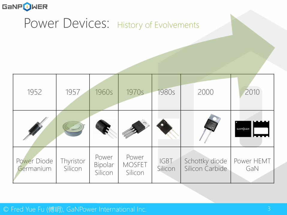
1952 1957 1960s 1970s 1980s 2000 2010
Power Diode Germanium
ThyristorSilicon
Power BipolarSilicon
Power MOSFET Silicon
IGBTSilicon
Schottky diodeSilicon Carbide
Power HEMTGaN
Power Devices: History of Evolvements
4© Fred Yue Fu (傅玥), GaNPower International Inc.
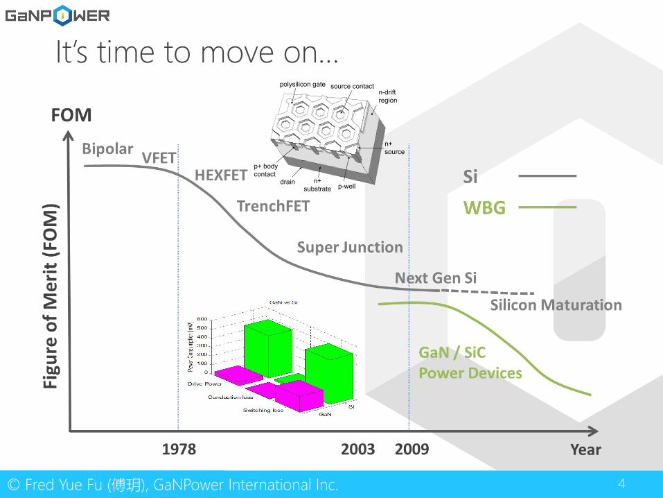
It’s time to move on…
drain n+substrate
n-drift region
p+ body contact
polysilicon gate source contact
n+ source
p-well
5© Fred Yue Fu (傅玥), GaNPower International Inc.
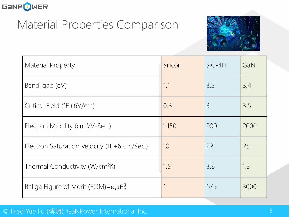
Material Properties Comparison
Material Property Silicon SiC-4H GaN
Band-gap (eV) 1.1 3.2 3.4
Critical Field (1E+6V/cm) 0.3 3 3.5
Electron Mobility (cm2/V-Sec.) 1450 900 2000
Electron Saturation Velocity (1E+6 cm/Sec.) 10 22 25
Thermal Conductivity (W/cm2K) 1.5 3.8 1.3
Baliga Figure of Merit (FOM)=ε"µE%& 1 675 3000

6© Fred Yue Fu (傅玥), GaNPower International Inc.
WBG Power Devices: Applications
GaN HEMT Silicon Super
Junction MOSFET
Encroaching
SiC MOSFET Silicon IGBTEncroaching
Source: Yole Development: How power electronics will reshape to meet 21st century challenges? ISPSD 2015
7© Fred Yue Fu (傅玥), GaNPower International Inc.
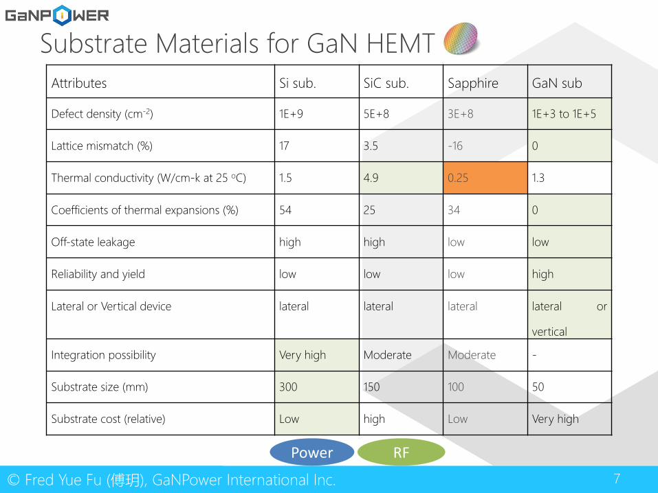
Attributes Si sub. SiC sub. Sapphire GaN sub
Defect density (cm-2) 1E+9 5E+8 3E+8 1E+3 to 1E+5
Lattice mismatch (%) 17 3.5 -16 0
Thermal conductivity (W/cm-k at 25 oC) 1.5 4.9 0.25 1.3
Coefficients of thermal expansions (%) 54 25 34 0
Off-state leakage high high low low
Reliability and yield low low low high
Lateral or Vertical device lateral lateral lateral lateral or
vertical
Integration possibility Very high Moderate Moderate -
Substrate size (mm) 300 150 100 50
Substrate cost (relative) Low high Low Very high
Substrate Materials for GaN HEMT
Power RF
8© Fred Yue Fu (傅玥), GaNPower International Inc.
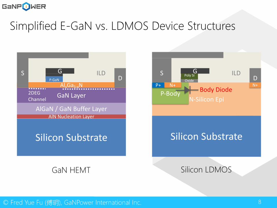
GaN HEMT Silicon LDMOS
Simplified E-GaN vs. LDMOS Device Structures
Silicon Substrate
SD
ILDOxide
N-Silicon Epi
Poly SiG
P-BodyN+P+ N+
Body Diode
Silicon Substrate
AlN Nucleation Layer
GaN LayerAlxGa1-xN
SD
2DEG Channel
G ILDP-GaN
AlGaN / GaN Buffer Layer
9© Fred Yue Fu (傅玥), GaNPower International Inc.
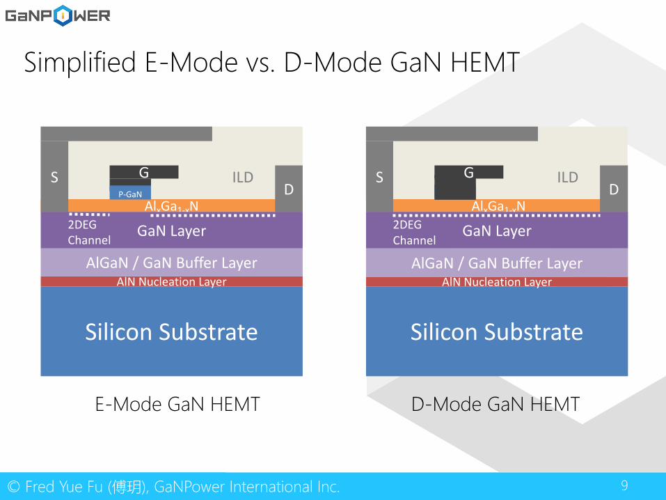
Simplified E-Mode vs. D-Mode GaN HEMT
E-Mode GaN HEMT D-Mode GaN HEMT
AlxGa1-xN
SD
ILDP-GaN
AlxGa1-xN
SD
G ILDP-GaN
Silicon Substrate
AlN Nucleation Layer
GaN Layer2DEG Channel
AlGaN / GaN Buffer Layer
Silicon Substrate
AlN Nucleation Layer
GaN Layer2DEG Channel
AlGaN / GaN Buffer Layer
G
10© Fred Yue Fu (傅玥), GaNPower International Inc.
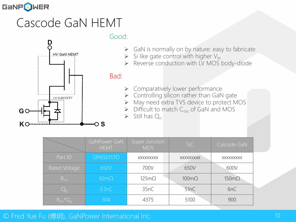
GaNPower GaNHEMT
Super Junction MOS
SiC Cascode GaN
Part ID GPI65015TO xxxxxxxxx xxxxxxxxx xxxxxxxxx
Rated Voltage 650V 700V 650V 600V
Ron 92mΩ 125mΩ 100mΩ 150mΩ
Qg 3.3nC 35nC 51nC 6nC
Ron*Qg 304 4375 5100 900
Good:
Ø GaN is normally on by nature: easy to fabricateØ Si like gate control with higher VthØ Reverse conduction with LV MOS body-diode
Bad:
Ø Comparatively lower performanceØ Controlling silicon rather than GaN gateØ May need extra TVS device to protect MOSØ Difficult to match Coss of GaN and MOSØ Still has Qrr
Cascode GaN HEMT
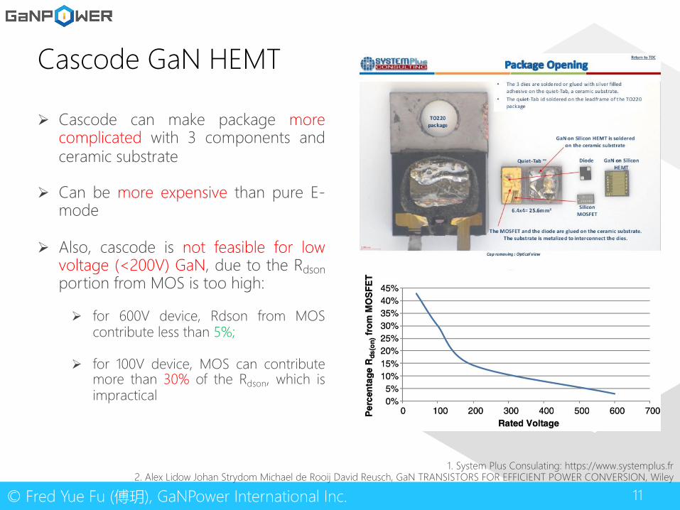
11© Fred Yue Fu (傅玥), GaNPower International Inc.
Cascode GaN HEMT
Ø Cascode can make package morecomplicated with 3 components andceramic substrate
Ø Can be more expensive than pure E-mode
Ø Also, cascode is not feasible for lowvoltage (<200V) GaN, due to the Rdsonportion from MOS is too high:
Ø for 600V device, Rdson from MOScontribute less than 5%;
Ø for 100V device, MOS can contributemore than 30% of the Rdson, which isimpractical
1. System Plus Consulating: https://www.systemplus.fr2. Alex Lidow Johan Strydom Michael de Rooij David Reusch, GaN TRANSISTORS FOR EFFICIENT POWER CONVERSION, Wiley
12© Fred Yue Fu (傅玥), GaNPower International Inc.
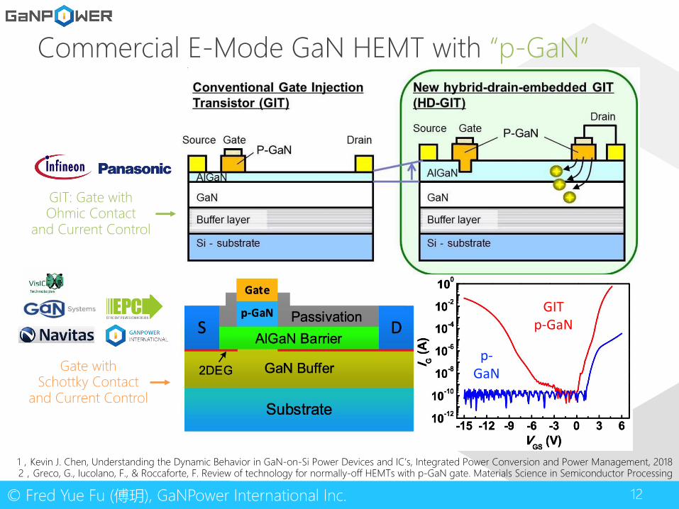
Commercial E-Mode GaN HEMT with “p-GaN”
GIT: Gate withOhmic Contact
and Current Control
Gate withSchottky Contact
and Current Control
1,Kevin J. Chen, Understanding the Dynamic Behavior in GaN-on-Si Power Devices and IC’s, Integrated Power Conversion and Power Management, 20182,Greco, G., Iucolano, F., & Roccaforte, F. Review of technology for normally-off HEMTs with p-GaN gate. Materials Science in Semiconductor Processing
GITp-GaN
p-GaN
13© Fred Yue Fu (傅玥), GaNPower International Inc.
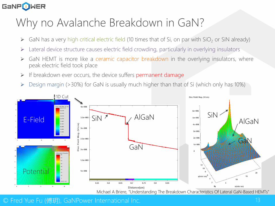
Why no Avalanche Breakdown in GaN?Ø GaN has a very high critical electric field (10 times that of Si, on par with SiO2 or SiN already)
Ø Lateral device structure causes electric field crowding, particularly in overlying insulators
Ø GaN HEMT is more like a ceramic capacitor breakdown in the overlying insulators, wherepeak electric field took place
Ø If breakdown ever occurs, the device suffers permanent damage
Ø Design margin (>30%) for GaN is usually much higher than that of Si (which only has 10%)
Michael A Briere, “Understanding The Breakdown Characteristics Of Lateral GaN-Based HEMTs”
Potential
E-FieldSiN
AlGaN
GaNGaN
AlGaNSiN
1D Cut
14© Fred Yue Fu (傅玥), GaNPower International Inc.
Why no P-type GaN HEMT Like PMOS?
Ø Si has both NMOS and PMOS, for NMOS, current is carried by electrons while inPMOS, current is carried by the holes
Ø However, for GaN HEMT, there is no P-type GaN HEMT yet
Ø First, ion implantation and subsequent annealing of magnesium in GaN is verydifficult to achieve
Ø Second, hole mobility in GaN is very low (30 cm2/Vs for holes vs. 2000 cm2/Vs forelectrons)
Ø GaN monolithic ICs are realized either by using complementary E-mode and D-mode GaN, or using E-mode GaN only

15© Fred Yue Fu (傅玥), GaNPower International Inc.
Why E-mode GaN Vg-max is Limited to 7V
0 1 2 3 4 5 6 7 8 9 10 11 12 13 14 15 16
1E-9
1E-8
1E-7
1E-6
1E-5
1E-4
1E-3
0.01
0.1
1
Ig (A
)
Vg (V)
Gate Leakage
Ø Unlike a silicon MOS, the P-GaN / AlGaN / GaN canbe viewed as a PIN diode structure with a depletionregion
Ø With in-situ doped p-type dopant (Magnesium) forp-GaN layer, the depletion region extends over thethickness of the GaN 2DEG channel for Vg=0V, thusinterrupts the channel below the gate region
Ø When a positive gate bias is applied, the 2DEGchannel is re-established, yielding to on-stateconditions
Ø Gate leakage current increases with increasing gatevoltage. Voltage beyond 7V will results higher gateleakage current
Ø For the P-GaN / AlGaN / GaN gate stack, a TDDB(Time Dependent Dielectric Breakdown) needs to beanalyzed for proper max gate voltage with long termreliability concerns
Ø It has been determined that maximum rating of6~7V for p-GaN HEMT is most appropriate
AlxGa1-xN
SD
G ILDP-GaN
Silicon Substrate
AlN Nucleation Layer
GaN Layer2DEG Channel
AlGaN / GaN Buffer Layer
16© Fred Yue Fu (傅玥), GaNPower International Inc.
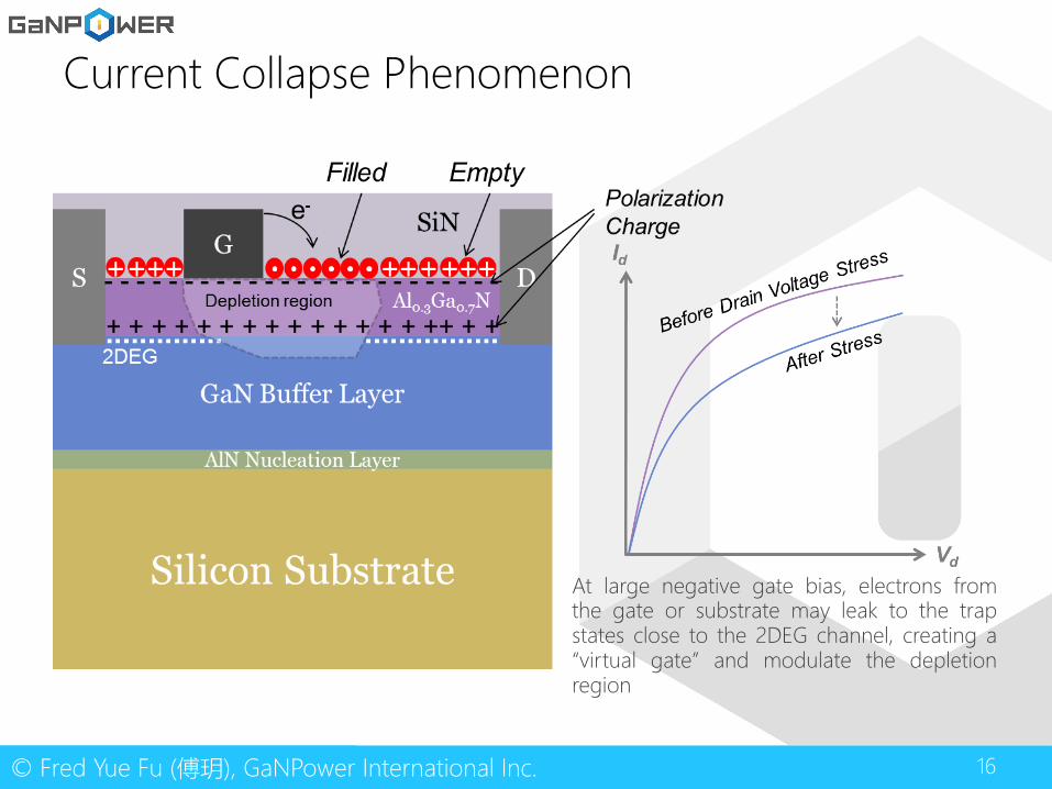
Current Collapse Phenomenon
At large negative gate bias, electrons fromthe gate or substrate may leak to the trapstates close to the 2DEG channel, creating a“virtual gate” and modulate the depletionregion
17© Fred Yue Fu (傅玥), GaNPower International Inc.
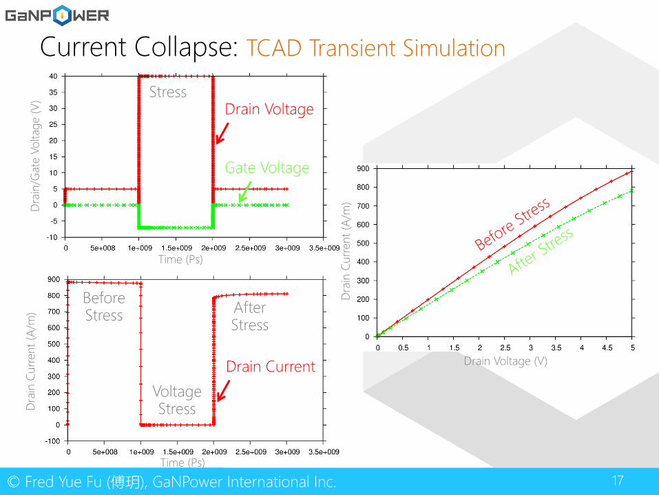
Current Collapse: TCAD Transient Simulation
Time (Ps)
Dra
in/G
ate
Volta
ge (V
)
Drain Voltage
Gate Voltage
Stress
Drain Voltage (V)D
rain
Cur
rent
(A/m
)
Before Stress
After S
tress
Time (Ps)
Dra
in C
urre
nt (A
/m)
Drain Current
Before Stress After
Stress
Voltage Stress

18© Fred Yue Fu (傅玥), GaNPower International Inc.
Contents
Ø Session 1: GaN devices basics
Ø GaN, An IntroductionØ GaN Design, Fabrication and TestingØ GaN Compact Modeling and Reliability
Ø Session 2: GaN Gate Driving
Ø Session 3: GaN Applications

19© Fred Yue Fu (傅玥), GaNPower International Inc.
Basic Semiconductor Materials
Final Power Supply Products
SubstrateEpi-waferFabrications
GaN Power Device Supply Chain
PCB AssemblyUL, CE, CCC Certification
GaNPower 6 inch GaN Wafer (real photo)
PackagingTesting
Packaged GaN Devices

20© Fred Yue Fu (傅玥), GaNPower International Inc.
How GaN Power Devices Are Fabricated?
Device Design and
LayoutCircuit
Probing(Wafer level
testing)
Packaging (Wire-bond)
Packaging (Bumping)
New Lead frame Design
1
Epitaxial Wafer
1Device
Fabrication
2 3
4
4
4
Final Testing
(Packaging Level)
5

21© Fred Yue Fu (傅玥), GaNPower International Inc.
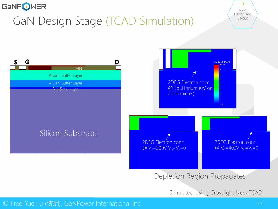
GaN Design Stage (TCAD Simulation)
1
P-GaN HEMT Device Structure
Device StructureZoom-in
1 2P-GaN
2DEG
Vgs@0V 1
2Conduction Band
Valence Band
Fermi Level
Conduction Band
Valence Band
Fermi LevelP-GaN
AlGaN GaN AlGaN GaN
- . 1
Simulated Using Crosslight NovaTCAD
Vgs@6V
Conduction Band
Valence Band
Quasi-Fermi Level
P-GaNAlGaN GaN
S G D
1Vgs@0V
G
(*Simulated using Ohmic Gate Contact)
AlGaN
GaN
2DEG2DEG
22© Fred Yue Fu (傅玥), GaNPower International Inc.
GaN Design Stage (TCAD Simulation)
1
Silicon Substrate
AlN Seed LayerAlGaN Buffer Layer
AlGaN Buffer Layer
S G DAlN
2DEG Electron conc. @ Equilibrium (0V on all Terminals)
2DEG Electron conc. @ Vd=200V Vg=Vs=0
2DEG Electron conc. @ Vd=400V Vg=Vs=0
Simulated Using Crosslight NovaTCAD
Depletion Region Propagates
23© Fred Yue Fu (傅玥), GaNPower International Inc.
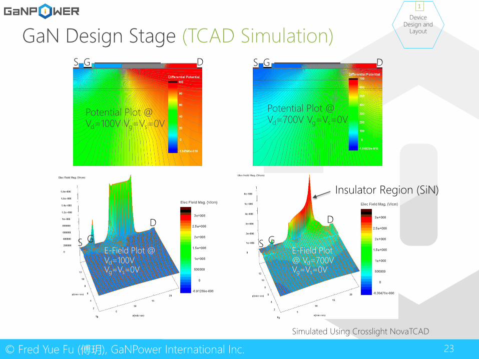
Potential Plot @ Vd=700V Vg=Vs=0V
Potential Plot @ Vd=100V Vg=Vs=0V
E-Field Plot @ Vd=700V Vg=Vs=0V
E-Field Plot @ Vd=100V Vg=Vs=0V
GaN Design Stage (TCAD Simulation)
Simulated Using Crosslight NovaTCAD
1
Insulator Region (SiN)
S G D S G D
S G
D
S G
D
24© Fred Yue Fu (傅玥), GaNPower International Inc.
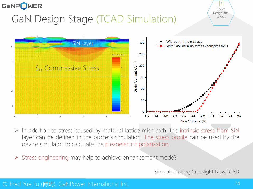
1
GaN Design Stage (TCAD Simulation)
Sxx Compressive Stress
Ø In addition to stress caused by material lattice mismatch, the intrinsic stress from SiNlayer can be defined in the process simulation. The stress profile can be used by thedevice simulator to calculate the piezoelectric polarization.
Ø Stress engineering may help to achieve enhancement mode?
Simulated Using Crosslight NovaTCAD
SiN Layer
25© Fred Yue Fu (傅玥), GaNPower International Inc.
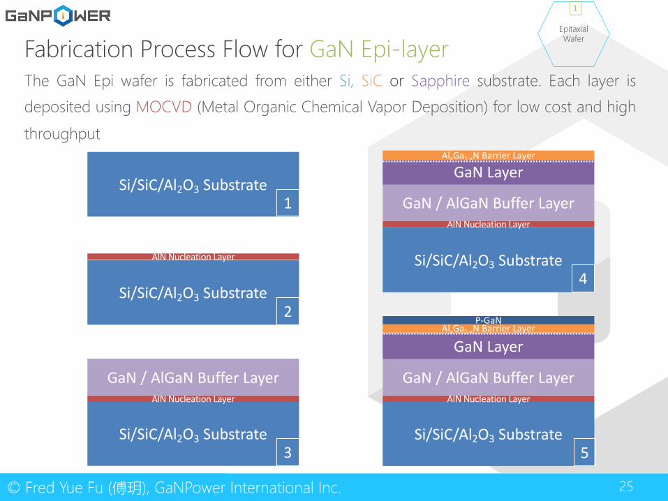
Fabrication Process Flow for GaN Epi-layer
Si/SiC/Al2O3 Substrate
AlN Nucleation Layer
P-GaN
Si/SiC/Al2O3 Substrate
Si/SiC/Al2O3 Substrate
AlN Nucleation Layer
Si/SiC/Al2O3 Substrate
AlN Nucleation Layer
GaN / AlGaN Buffer Layer
Si/SiC/Al2O3 Substrate
GaN / AlGaN Buffer Layer1
2
3
4
5
The GaN Epi wafer is fabricated from either Si, SiC or Sapphire substrate. Each layer is
deposited using MOCVD (Metal Organic Chemical Vapor Deposition) for low cost and high
throughput
1
GaN Layer
GaN / AlGaN Buffer Layer
GaN Layer
AlxGa1-xN Barrier Layer
AlxGa1-xN Barrier Layer
AlN Nucleation Layer
26© Fred Yue Fu (傅玥), GaNPower International Inc.
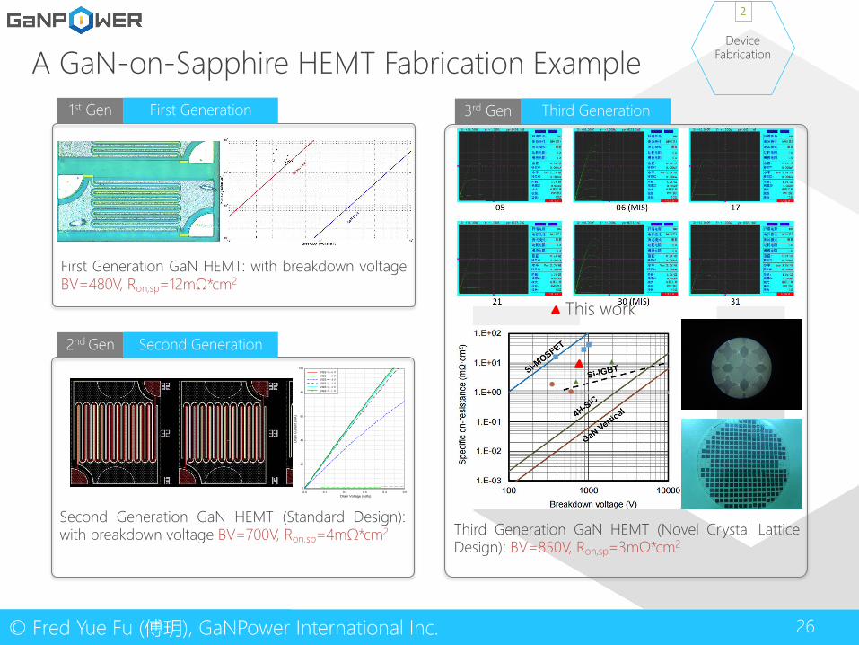
A GaN-on-Sapphire HEMT Fabrication Example
First Generation GaN HEMT: with breakdown voltageBV=480V, Ron,sp=12mΩ*cm2
1st Gen First Generation
Third Generation GaN HEMT (Novel Crystal LatticeDesign): BV=850V, Ron,sp=3mΩ*cm2
This work
3rd Gen Third Generation
Second Generation GaN HEMT (Standard Design):with breakdown voltage BV=700V, Ron,sp=4mΩ*cm2
Drain Voltage (volts)0.0 0.1 0.2 0.3 0.4 0.5
Dra
in C
urre
nt (m
A)
0
20
40
60
80
100VGS = - 6 VVGS = - 5 VVGS = - 4 VVGS = - 3 VVGS = - 2 VVGS = - 1 V
2nd Gen Second Generation
2
27© Fred Yue Fu (傅玥), GaNPower International Inc.
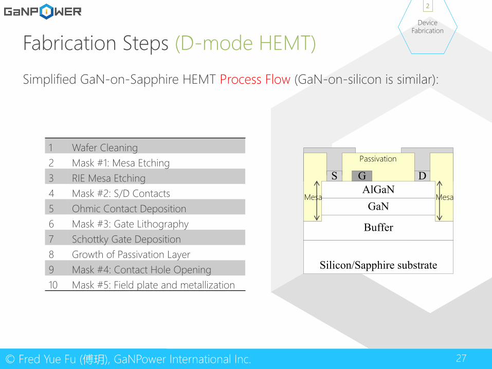
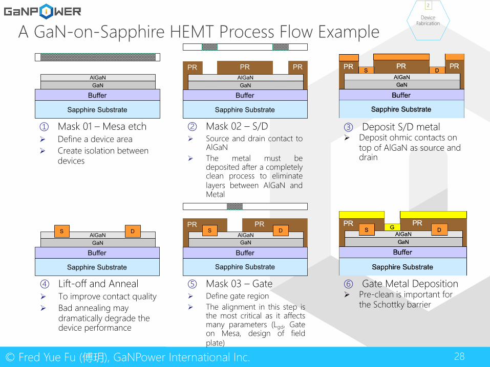
Fabrication Steps (D-mode HEMT)
1 Wafer Cleaning2 Mask #1: Mesa Etching3 RIE Mesa Etching4 Mask #2: S/D Contacts5 Ohmic Contact Deposition6 Mask #3: Gate Lithography7 Schottky Gate Deposition8 Growth of Passivation Layer9 Mask #4: Contact Hole Opening10 Mask #5: Field plate and metallization
Simplified GaN-on-Sapphire HEMT Process Flow (GaN-on-silicon is similar):
Silicon/Sapphire substrate
GaN
Buffer
AlGaNS DG
2
Mesa
Passivation
Mesa
28© Fred Yue Fu (傅玥), GaNPower International Inc.
① Mask 01 – Mesa etchØ Define a device areaØ Create isolation between
devices
Sapphire Substrate
BufferGaN
AlGaN
PR PRPR
Sapphire Substrate
BufferGaN
AlGaN
② Mask 02 – S/D Ø Source and drain contact to
AlGaNØ The metal must be
deposited after a completelyclean process to eliminatelayers between AlGaN andMetal
A GaN-on-Sapphire HEMT Process Flow Example
③ Deposit S/D metalØ Deposit ohmic contacts on
top of AlGaN as source and drain
Sapphire Substrate
BufferGaN
AlGaNS D
④ Lift-off and AnnealØ To improve contact qualityØ Bad annealing may
dramatically degrade the device performance
⑤ Mask 03 – GateØ Define gate regionØ The alignment in this step is
the most critical as it affectsmany parameters (Lgd, Gateon Mesa, design of fieldplate)
⑥ Gate Metal DepositionØ Pre-clean is important for
the Schottky barrier
PR PR
Sapphire Substrate
BufferGaN
AlGaNS D
2
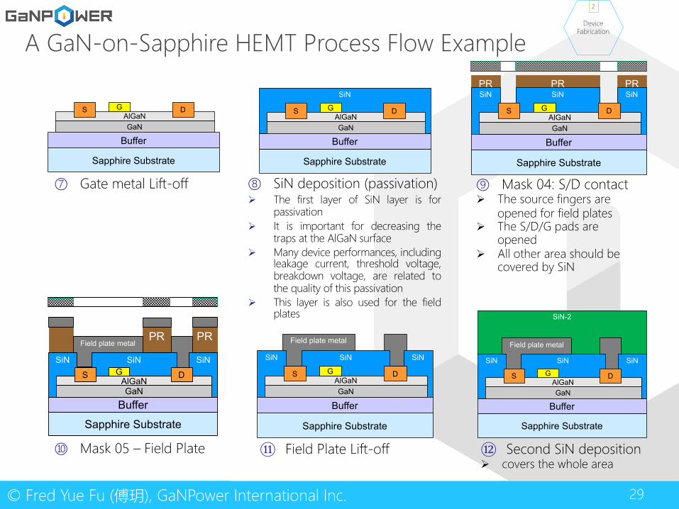
29© Fred Yue Fu (傅玥), GaNPower International Inc.
⑦ Gate metal Lift-off ⑧ SiN deposition (passivation)Ø The first layer of SiN layer is for
passivationØ It is important for decreasing the
traps at the AlGaN surfaceØ Many device performances, including
leakage current, threshold voltage,breakdown voltage, are related tothe quality of this passivation
Ø This layer is also used for the fieldplates
⑨ Mask 04: S/D contactØ The source fingers are
opened for field platesØ The S/D/G pads are
openedØ All other area should be
covered by SiN
⑪ Field Plate Lift-off
Sapphire Substrate
BufferGaN
AlGaNS DG
SiN
Sapphire Substrate
BufferGaN
AlGaNGS D
PR PRPRSiNSiNSiN
Sapphire Substrate
BufferGaN
AlGaNS DG
PR PRField plate metal
SiNSiNSiN
Sapphire Substrate
BufferGaN
AlGaNS DG
Field plate metal
SiNSiNSiN
Sapphire Substrate
BufferGaN
AlGaNS DG
SiN-2
Field plate metal
SiNSiNSiN
Sapphire Substrate
BufferGaN
AlGaNS DG
⑫ Second SiN depositionØ covers the whole area
⑩ Mask 05 – Field Plate
2
A GaN-on-Sapphire HEMT Process Flow Example
30© Fred Yue Fu (傅玥), GaNPower International Inc.
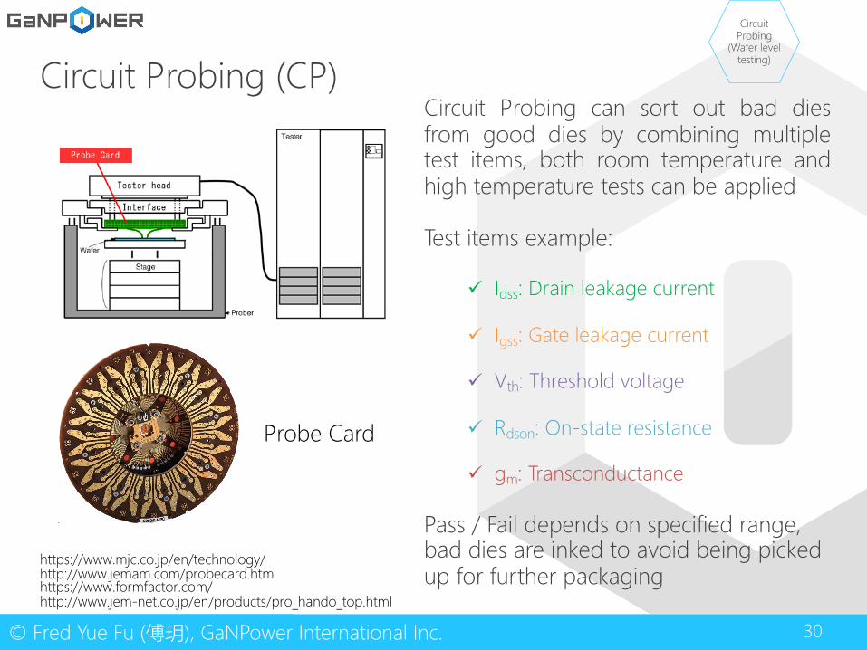
Circuit Probing (CP)
http://www.jemam.com/probecard.htmhttps://www.mjc.co.jp/en/technology/
https://www.formfactor.com/http://www.jem-net.co.jp/en/products/pro_hando_top.html
Probe Card
Circuit Probing can sort out bad diesfrom good dies by combining multipletest items, both room temperature andhigh temperature tests can be applied
Test items example:
ü Idss: Drain leakage current
ü Igss: Gate leakage current
ü Vth: Threshold voltage
ü Rdson: On-state resistance
ü gm: Transconductance
Pass / Fail depends on specified range, bad dies are inked to avoid being picked up for further packaging
)(
)
31© Fred Yue Fu (傅玥), GaNPower International Inc.
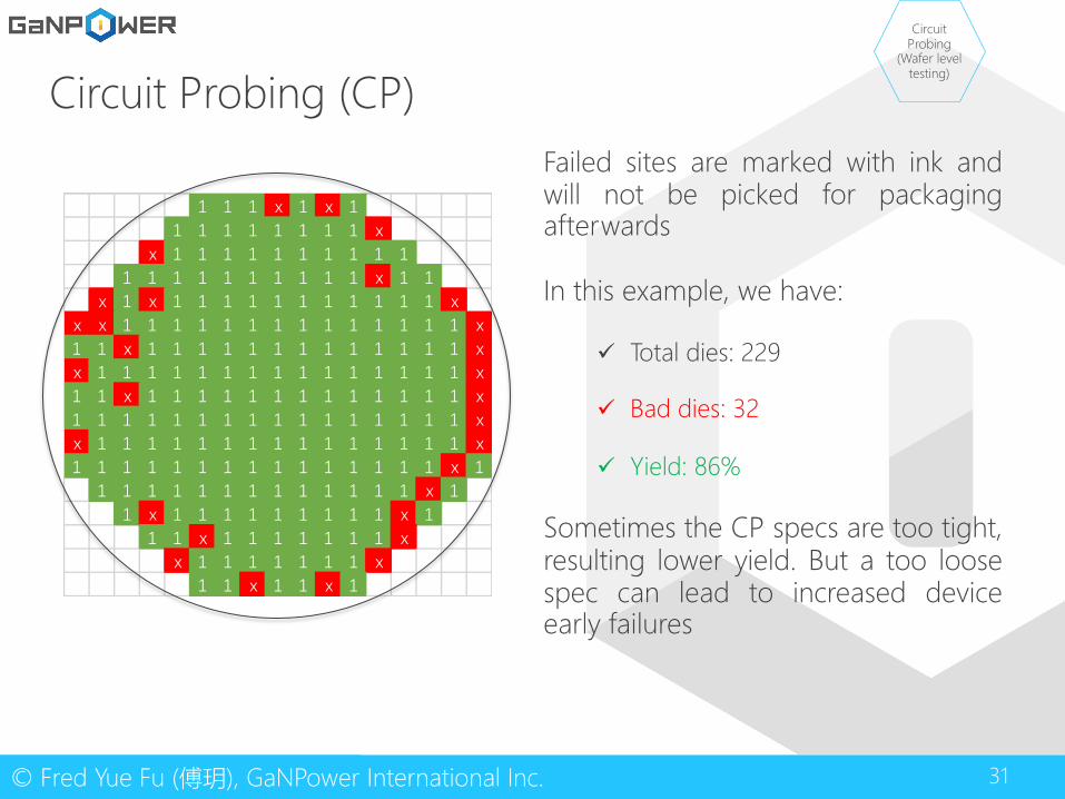
Circuit Probing (CP)Failed sites are marked with ink andwill not be picked for packagingafterwards
In this example, we have:
ü Total dies: 229
ü Bad dies: 32
ü Yield: 86%
Sometimes the CP specs are too tight,resulting lower yield. But a too loosespec can lead to increased deviceearly failures
)(
)
32© Fred Yue Fu (傅玥), GaNPower International Inc.
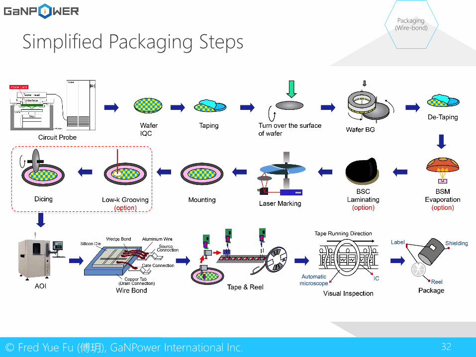
Simplified Packaging Steps ) )
( -
33© Fred Yue Fu (傅玥), GaNPower International Inc.
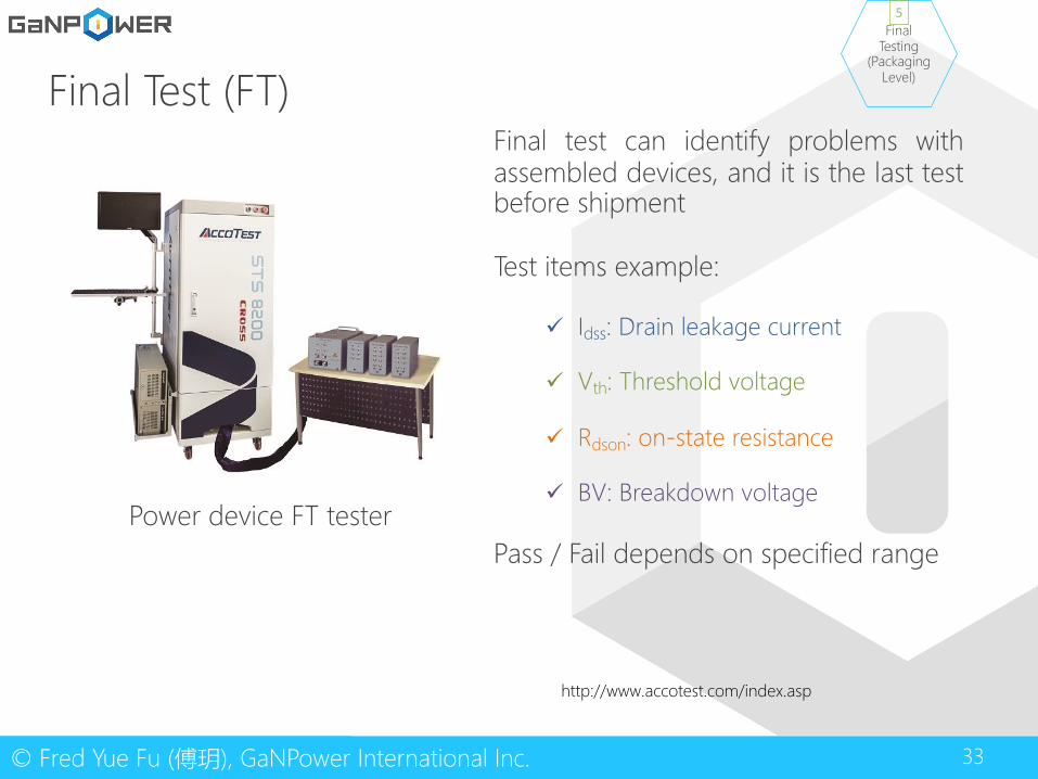
Final Test (FT)
http://www.accotest.com/index.asp
Final test can identify problems withassembled devices, and it is the last testbefore shipment
Test items example:
ü Idss: Drain leakage current
ü Vth: Threshold voltage
ü Rdson: on-state resistance
ü BV: Breakdown voltage
Pass / Fail depends on specified rangePower device FT tester
)) (() (
5
34© Fred Yue Fu (傅玥), GaNPower International Inc.
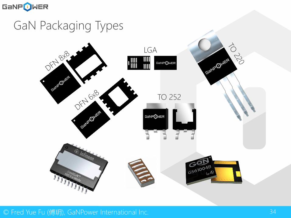
GaN Packaging Types
DFN 8x
8
DFN 6x
8
LGA
TO 252
TO 220

35© Fred Yue Fu (傅玥), GaNPower International Inc.
GaN Device Parameter Testing
ü Static (DC) parameters testing
Ø Rdson, Vth, BV, Idss, Igss, Vsd, Rg, etc…
ü Dynamic parameters testing
Ø Ciss, Crss, Coss, Qg, Qgs, Qgd, Qrr, etc…
ü Double pulse testing (for dynamic parameters)
Ø Tr, Tf, Td, dv/dt, etc…
ü Thermal testing
Ø Rthjc, Rthja, etc…
ü SOA testing
36© Fred Yue Fu (傅玥), GaNPower International Inc.
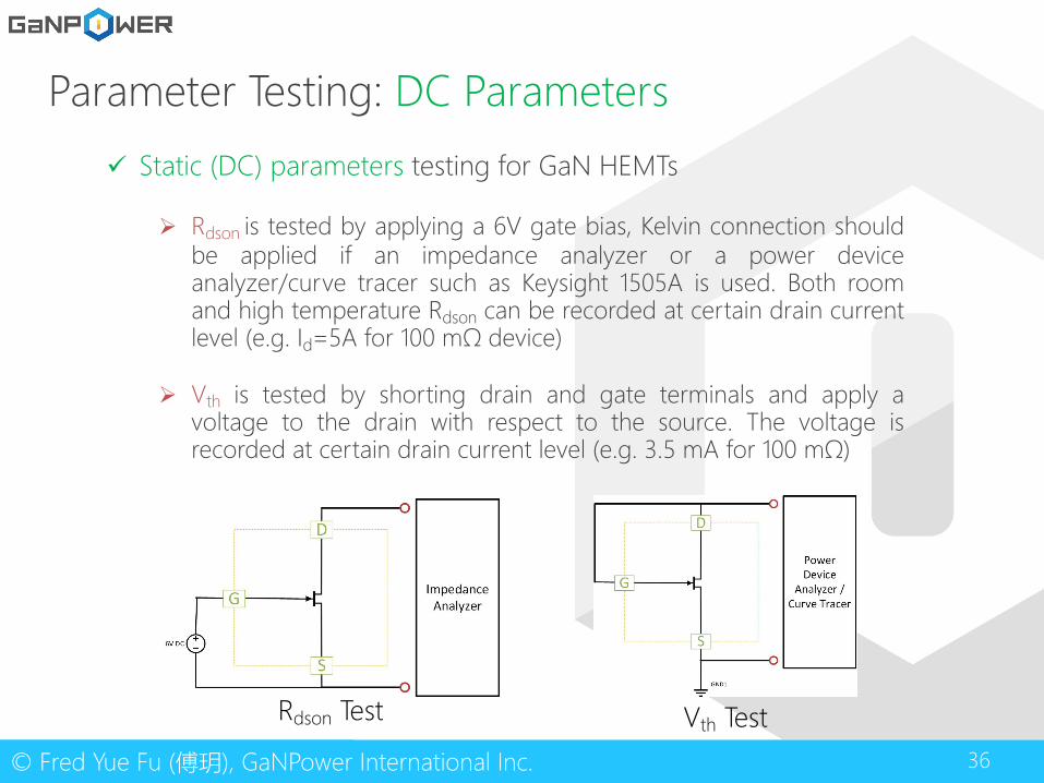
Parameter Testing: DC Parameters
ü Static (DC) parameters testing for GaN HEMTs
Ø Rdson is tested by applying a 6V gate bias, Kelvin connection shouldbe applied if an impedance analyzer or a power deviceanalyzer/curve tracer such as Keysight 1505A is used. Both roomand high temperature Rdson can be recorded at certain drain currentlevel (e.g. Id=5A for 100 mΩ device)
Ø Vth is tested by shorting drain and gate terminals and apply avoltage to the drain with respect to the source. The voltage isrecorded at certain drain current level (e.g. 3.5 mA for 100 mΩ)
Rdson Test Vth Test
37© Fred Yue Fu (傅玥), GaNPower International Inc.
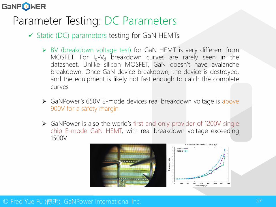
Parameter Testing: DC Parametersü Static (DC) parameters testing for GaN HEMTs
Ø BV (breakdown voltage test) for GaN HEMT is very different fromMOSFET. For Id-Vd breakdown curves are rarely seen in thedatasheet. Unlike silicon MOSFET, GaN doesn’t have avalanchebreakdown. Once GaN device breakdown, the device is destroyed,and the equipment is likely not fast enough to catch the completecurves
Ø GaNPower’s 650V E-mode devices real breakdown voltage is above900V for a safety margin
Ø GaNPower is also the world’s first and only provider of 1200V singlechip E-mode GaN HEMT, with real breakdown voltage exceeding1500V
38© Fred Yue Fu (傅玥), GaNPower International Inc.
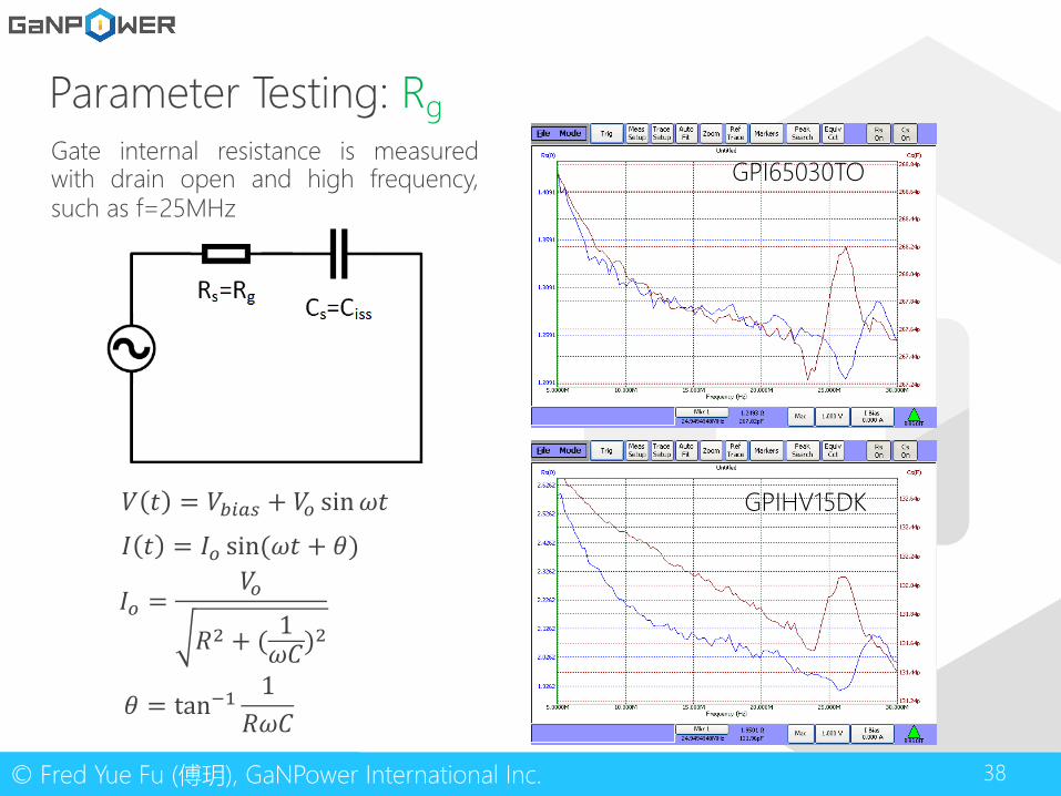
Parameter Testing: Rg
GPI65030TO
GPIHV15DK
Gate internal resistance is measuredwith drain open and high frequency,such as f=25MHz
𝑉 𝑡 = 𝑉,-./ + 𝑉1 sin𝜔𝑡𝐼 𝑡 = 𝐼1 sin(𝜔𝑡 + 𝜃)
𝐼1 =𝑉1
𝑅; + ( 1𝜔𝐶);
𝜃 = tan@A1
𝑅𝜔𝐶
39© Fred Yue Fu (傅玥), GaNPower International Inc.
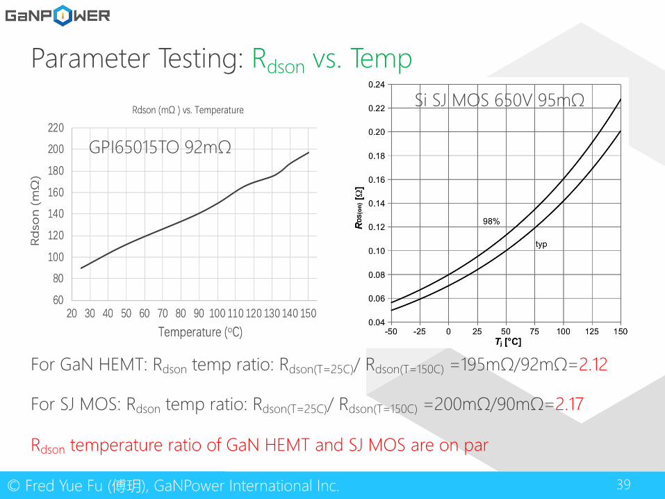
Parameter Testing: Rdson vs. Temp
For GaN HEMT: Rdson temp ratio: Rdson(T=25C)/ Rdson(T=150C) =195mΩ/92mΩ=2.12
For SJ MOS: Rdson temp ratio: Rdson(T=25C)/ Rdson(T=150C) =200mΩ/90mΩ=2.17
Rdson temperature ratio of GaN HEMT and SJ MOS are on par
Si SJ MOS 650V 95mΩ
GPI65015TO 92mΩ
40© Fred Yue Fu (傅玥), GaNPower International Inc.
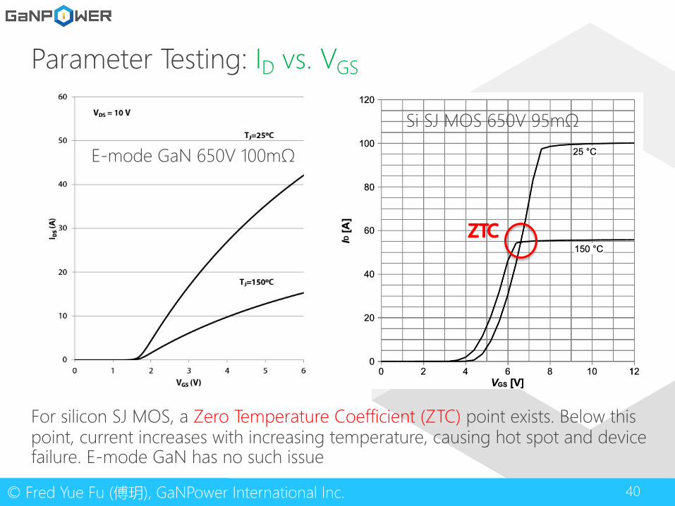
Parameter Testing: ID vs. VGS
ZTC
For silicon SJ MOS, a Zero Temperature Coefficient (ZTC) point exists. Below this point, current increases with increasing temperature, causing hot spot and device failure. E-mode GaN has no such issue
Si SJ MOS 650V 95mΩ
E-mode GaN 650V 100mΩ
41© Fred Yue Fu (傅玥), GaNPower International Inc.
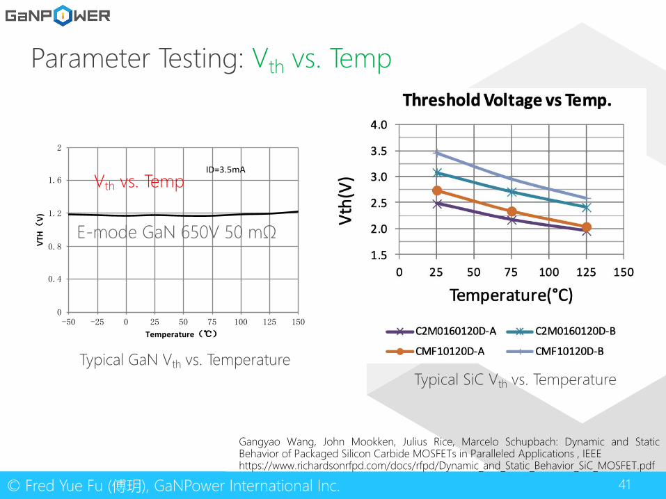
Parameter Testing: Vth vs. Temp
VTHV)
Temperature
ID=3.5mAVth vs. Temp
E-mode GaN 650V 50 mΩ
Gangyao Wang, John Mookken, Julius Rice, Marcelo Schupbach: Dynamic and StaticBehavior of Packaged Silicon Carbide MOSFETs in Paralleled Applications , IEEEhttps://www.richardsonrfpd.com/docs/rfpd/Dynamic_and_Static_Behavior_SiC_MOSFET.pdf
Typical SiC Vth vs. TemperatureTypical GaN Vth vs. Temperature
42© Fred Yue Fu (傅玥), GaNPower International Inc.
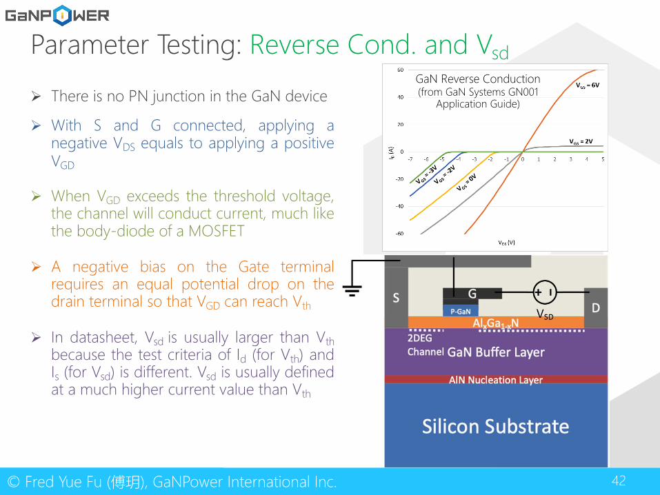
Parameter Testing: Reverse Cond. and VsdGaN Reverse Conduction(from GaN Systems GN001
Application Guide)Ø There is no PN junction in the GaN device
Ø With S and G connected, applying anegative VDS equals to applying a positiveVGD
Ø When VGD exceeds the threshold voltage,the channel will conduct current, much likethe body-diode of a MOSFET
Ø A negative bias on the Gate terminalrequires an equal potential drop on thedrain terminal so that VGD can reach Vth
Ø In datasheet, Vsd is usually larger than Vthbecause the test criteria of Id (for Vth) andIs (for Vsd) is different. Vsd is usually definedat a much higher current value than Vth
43© Fred Yue Fu (傅玥), GaNPower International Inc.
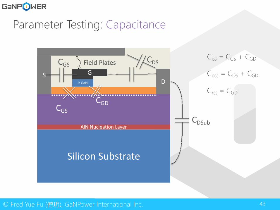
Parameter Testing: Capacitance
Silicon Substrate
AlN Nucleation Layer
SD
GField Plates
P-GaN
CDS
CDSub
CGD
CGSCiss = CGS + CGD
Coss = CDS + CGD
Crss = CGD
CGS
44© Fred Yue Fu (傅玥), GaNPower International Inc.
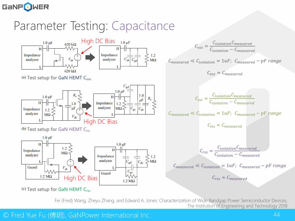
Parameter Testing: Capacitance
Fei (Fred) Wang, Zheyu Zhang, and Edward A. Jones: Characterization of Wide Bandgap Power Semiconductor Devices, The Institution of Engineering and Technology 2018
𝐶1// =𝐶-/1B.C-1D𝐶EF./GHFI𝐶-/1B.C-1D − 𝐶EF./GHFI
𝐶EF./GHFI ≪ 𝐶-/1B.C-1D = 1𝑢𝐹; 𝐶EF./GHFI ~ 𝑝𝐹 𝑟𝑎𝑛𝑔𝑒
𝐶1// ≈ 𝐶EF./GHFITest setup for GaN HEMT Coss
Test setup for GaN HEMT Ciss
Test setup for GaN HEMT Crss
𝐶-// =𝐶-/1B.C-1D𝐶EF./GHFI𝐶-/1B.C-1D − 𝐶EF./GHFI
𝐶EF./GHFI ≪ 𝐶-/1B.C-1D = 1𝑢𝐹; 𝐶EF./GHFI ~ 𝑝𝐹 𝑟𝑎𝑛𝑔𝑒
𝐶-// ≈ 𝐶EF./GHFI
𝐶H// =𝐶-/1B.C-1D𝐶EF./GHFI𝐶-/1B.C-1D − 𝐶EF./GHFI
𝐶EF./GHFI ≪ 𝐶-/1B.C-1D = 1𝑢𝐹; 𝐶EF./GHFI ~ 𝑝𝐹 𝑟𝑎𝑛𝑔𝑒
𝐶H// ≈ 𝐶EF./GHFI
High DC Bias
High DC Bias
High DC Bias
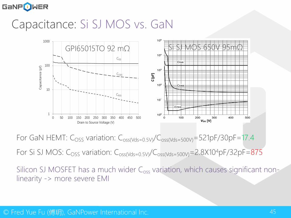
45© Fred Yue Fu (傅玥), GaNPower International Inc.
Si SJ MOS 650V 95mΩGPI65015TO 92 mΩ
For GaN HEMT: COSS variation: Coss(Vds=0.5V)/Coss(Vds=500V)=521pF/30pF=17.4
For Si SJ MOS: COSS variation: Coss(Vds=0.5V)/Coss(Vds=500V)=2.8X104pF/32pF=875
Silicon SJ MOSFET has a much wider Coss variation, which causes significant non-linearity -> more severe EMI
Capacitance: Si SJ MOS vs. GaN
46© Fred Yue Fu (傅玥), GaNPower International Inc.Drain
N DriftP-Body
N+ Substrate
P-Co
l
P-Co
l
Source/Body Metal
N+ N+
Gate
P-Body
P+ P+
N-Drift
Depl
etio
n re
gion
Depl
etio
n re
giond
Drain
N DriftP-Body
N+ SubstrateP-
Col
P-Co
l
Source/Body Metal
N+ N+
Gate
P-Body
P+ P+
Depletion Region
d
Drain
N DriftN-Drift
N DriftP-Body
N+ Substrate
P-Co
l
P-Co
l
Source/Body Metal
N+ N+
Gate
P-Body
P+ P+
Drain
N DriftP-Body
N+ Substrate
P-Co
l
P-Co
l
Source/Body Metal
P-Body
P+ P+
N-Drift
Depl
etio
n re
gion
Depl
etio
n re
giond
N+ N+
Gate
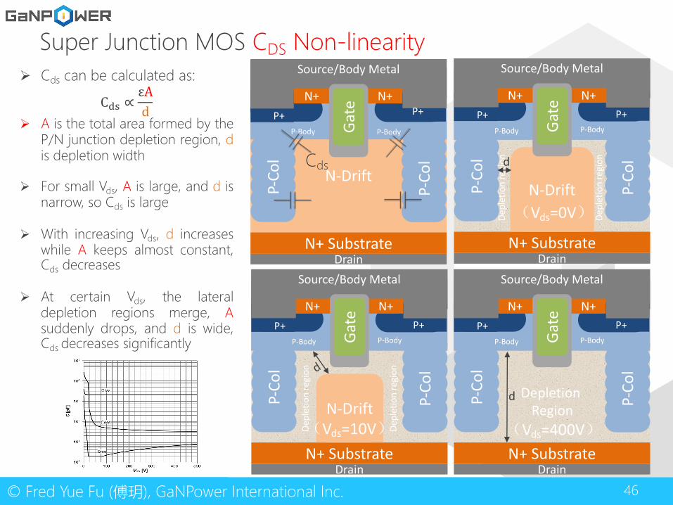
Super Junction MOS CDS Non-linearityØ Cds can be calculated as:
CX" ∝εAd
Ø A is the total area formed by theP/N junction depletion region, dis depletion width
Ø For small Vds, A is large, and d isnarrow, so Cds is large
Ø With increasing Vds, d increaseswhile A keeps almost constant,Cds decreases
Ø At certain Vds, the lateraldepletion regions merge, Asuddenly drops, and d is wide,Cds decreases significantly
(Vds=0V)
(Vds=10V) (Vds=400V)
Cds
47© Fred Yue Fu (傅玥), GaNPower International Inc.
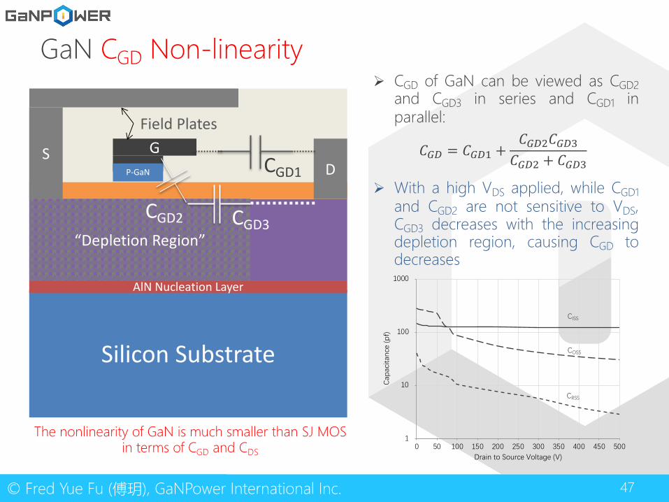
GaN CGD Non-linearity
SD
GField Plates
P-GaN CGD1
“Depletion Region”
CGD2 CGD3
Silicon Substrate
AlN Nucleation Layer
Ø CGD of GaN can be viewed as CGD2and CGD3 in series and CGD1 inparallel:
Ø With a high VDS applied, while CGD1and CGD2 are not sensitive to VDS,CGD3 decreases with the increasingdepletion region, causing CGD todecreases
𝐶\] = 𝐶\]A +𝐶\];𝐶\]&𝐶\]; + 𝐶\]&
The nonlinearity of GaN is much smaller than SJ MOS in terms of CGD and CDS
48© Fred Yue Fu (傅玥), GaNPower International Inc.
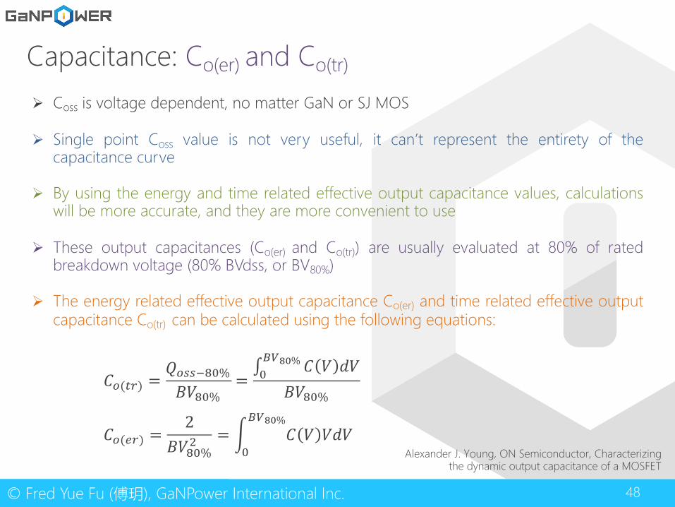
Capacitance: Co(er) and Co(tr)
Ø Coss is voltage dependent, no matter GaN or SJ MOS
Ø Single point Coss value is not very useful, it can’t represent the entirety of thecapacitance curve
Ø By using the energy and time related effective output capacitance values, calculationswill be more accurate, and they are more convenient to use
Ø These output capacitances (Co(er) and Co(tr)) are usually evaluated at 80% of ratedbreakdown voltage (80% BVdss, or BV80%)
Ø The energy related effective output capacitance Co(er) and time related effective outputcapacitance Co(tr) can be calculated using the following equations:
𝐶1(CH) =𝑄1//@_`%𝐵𝑉_`%
=∫defg% 𝐶 𝑉 𝑑𝑉
𝐵𝑉_`%
𝐶1(FH) =2
𝐵𝑉_`%;= j
`
defg%𝐶 𝑉 𝑉𝑑𝑉
Alexander J. Young, ON Semiconductor, Characterizing the dynamic output capacitance of a MOSFET
49© Fred Yue Fu (傅玥), GaNPower International Inc.
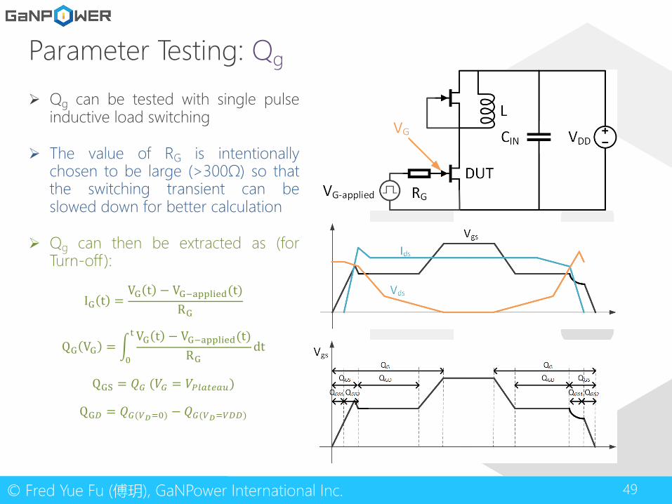
Parameter Testing: Qg
Ø Qg can be tested with single pulseinductive load switching
Ø The value of RG is intentionallychosen to be large (>300Ω) so thatthe switching transient can beslowed down for better calculation
Ø Qg can then be extracted as (forTurn-off ):
Il t =Vl t − Vl@noopqrX(t)
Rl
Ql Vl = j`
u Vl t − Vl@noopqrX(t)Rl
dt
Qlv = 𝑄\ (𝑉\ = 𝑉wB.CF.G)
Ql] = 𝑄\(exy`) − 𝑄\(exye]])
50© Fred Yue Fu (傅玥), GaNPower International Inc.
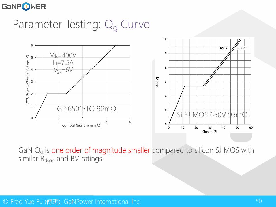
Parameter Testing: Qg Curve
Vds=400VId=7.5AVgs=6V
GPI65015TO 92mΩSi SJ MOS 650V 95mΩ
GaN Qg is one order of magnitude smaller compared to silicon SJ MOS with similar Rdson and BV ratings
51© Fred Yue Fu (傅玥), GaNPower International Inc.
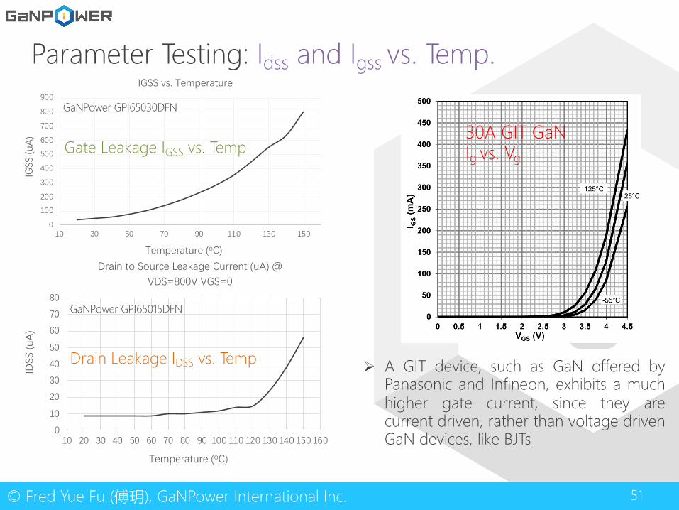
Parameter Testing: Idss and Igss vs. Temp.
# $!!%#%## $%
%
"#$%#!
GaNPower GPI65015DFN
GaNPower GPI65030DFN
Ø A GIT device, such as GaN offered byPanasonic and Infineon, exhibits a muchhigher gate current, since they arecurrent driven, rather than voltage drivenGaN devices, like BJTs
30A GIT GaNIg vs. Vg
Gate Leakage IGSS vs. Temp
Drain Leakage IDSS vs. Temp
52© Fred Yue Fu (傅玥), GaNPower International Inc.
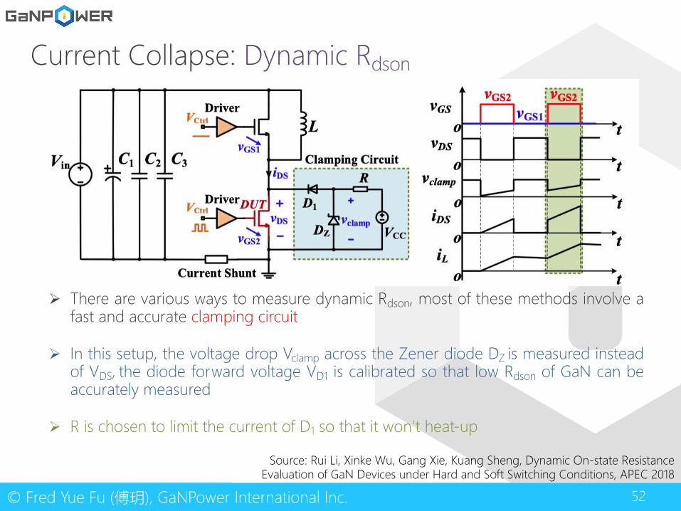
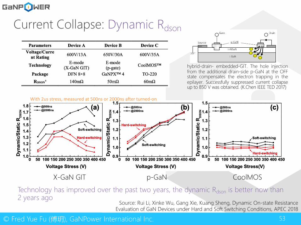
Current Collapse: Dynamic Rdson
Ø There are various ways to measure dynamic Rdson, most of these methods involve afast and accurate clamping circuit
Ø In this setup, the voltage drop Vclamp across the Zener diode DZ is measured insteadof VDS, the diode forward voltage VD1 is calibrated so that low Rdson of GaN can beaccurately measured
Ø R is chosen to limit the current of D1 so that it won’t heat-up
Source: Rui Li, Xinke Wu, Gang Xie, Kuang Sheng, Dynamic On-state Resistance Evaluation of GaN Devices under Hard and Soft Switching Conditions, APEC 2018
53© Fred Yue Fu (傅玥), GaNPower International Inc.
Current Collapse: Dynamic Rdson
X-GaN GIT p-GaN CoolMOS
Source: Rui Li, Xinke Wu, Gang Xie, Kuang Sheng, Dynamic On-state Resistance Evaluation of GaN Devices under Hard and Soft Switching Conditions, APEC 2018
Technology has improved over the past two years, the dynamic Rdson is better now than2 years ago
hybrid-drain- embedded-GIT. The hole injectionfrom the additional drain-side p-GaN at the OFFstate compensates the electron trapping in theepilayer. Successfully suppressed current collapseup to 850 V was obtained. (K.Chen IEEE TED 2017)
With 2us stress, measured at 500ns or 2000ns after turned-on
54© Fred Yue Fu (傅玥), GaNPower International Inc.
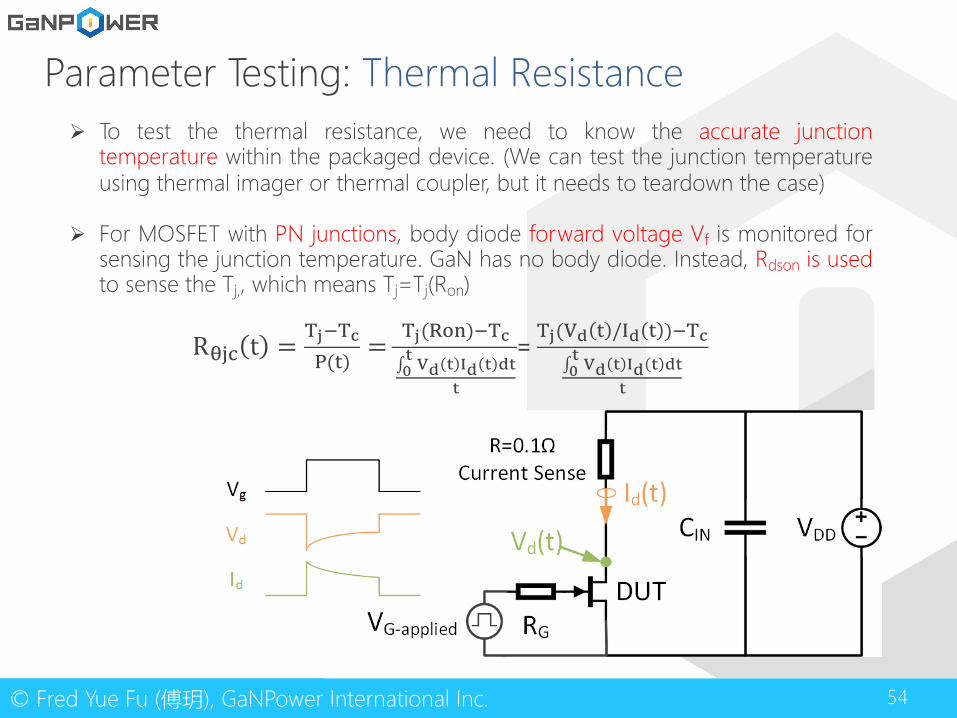
Parameter Testing: Thermal ResistanceØ To test the thermal resistance, we need to know the accurate junction
temperature within the packaged device. (We can test the junction temperatureusing thermal imager or thermal coupler, but it needs to teardown the case)
Ø For MOSFET with PN junctions, body diode forward voltage Vf is monitored forsensing the junction temperature. GaN has no body diode. Instead, Rdson is usedto sense the Tj,, which means Tj=Tj(Ron)
Rz% t =|@|~(u)
=|()@|~∫g
= |( u / u )@|~
∫g
55© Fred Yue Fu (傅玥), GaNPower International Inc.
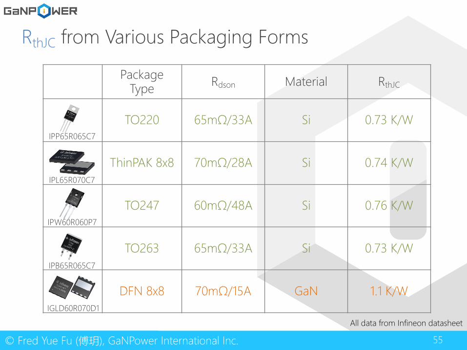
RthJC from Various Packaging Forms
Package Type Rdson Material RthJC
TO220 65mΩ/33A Si 0.73 K/W
ThinPAK 8x8 70mΩ/28A Si 0.74 K/W
TO247 60mΩ/48A Si 0.76 K/W
TO263 65mΩ/33A Si 0.73 K/W
DFN 8x8 70mΩ/15A GaN 1.1 K/W
All data from Infineon datasheet
IPW60R060P7
IPP65R065C7
IPL65R070C7
IPB65R065C7
IGLD60R070D1
56© Fred Yue Fu (傅玥), GaNPower International Inc.
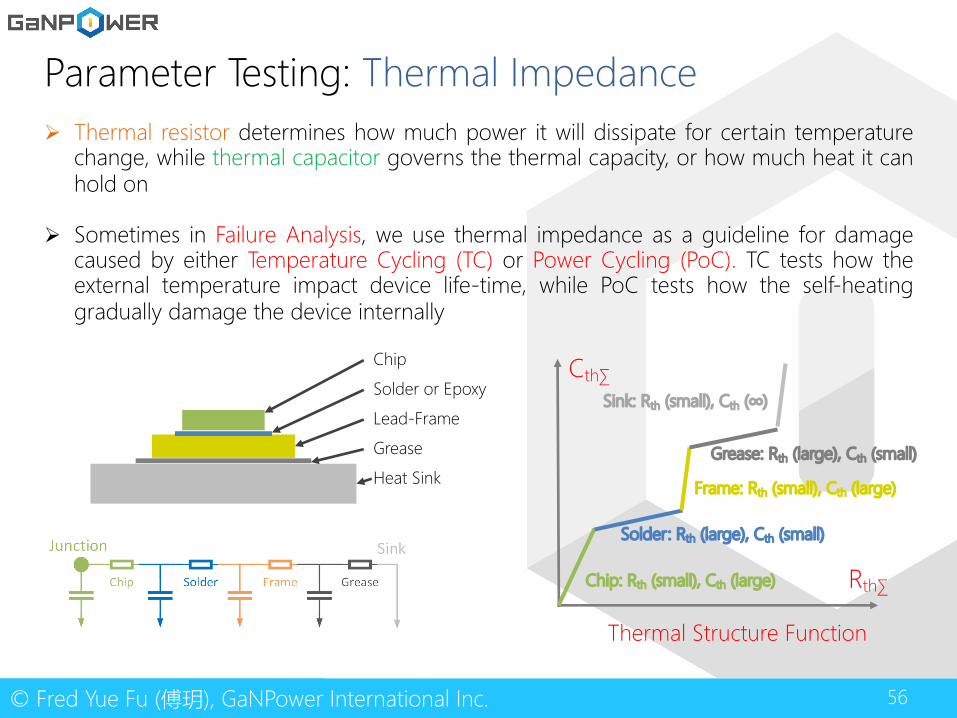
Parameter Testing: Thermal ImpedanceØ Thermal resistor determines how much power it will dissipate for certain temperature
change, while thermal capacitor governs the thermal capacity, or how much heat it canhold on
Ø Sometimes in Failure Analysis, we use thermal impedance as a guideline for damagecaused by either Temperature Cycling (TC) or Power Cycling (PoC). TC tests how theexternal temperature impact device life-time, while PoC tests how the self-heatinggradually damage the device internally
Chip
Solder or Epoxy
Lead-Frame
Grease
Heat Sink
Chip: Rth (small), Cth (large)
Solder: Rth (large), Cth (small)
Frame: Rth (small), Cth (large)
Grease: Rth (large), Cth (small)
Sink: Rth (small), Cth (∞)
Cth∑
Rth∑
Thermal Structure Function
57© Fred Yue Fu (傅玥), GaNPower International Inc.
Parameter Testing: Transient Thermal ImpedanceØ DC thermal impedance is the maximum thermal impedance at steady state
Ø The transient thermal impedance is a measure of how the device behaves when pulsed power isapplied to it. This is important for determining the behavior of low duty cycle, low frequencypulsed loads
Ø For the same power level, at short durations, the thermal impedance appears to be smaller
GaN systems: Transient thermal modeling of gallium nitride devices (http://tesint.com/docs/Transient_Thermal_Modeling_of_Electronic_Devices_Using_ElectroFlo.pdf)
58© Fred Yue Fu (傅玥), GaNPower International Inc.
How to Rate Continuous Current?
𝐼I/E. =𝑇E. −𝑇
𝑅I/1D@𝑅C
12 𝐼I/E.
; 𝑅I/1D@ =𝑇E. − 𝑇𝑅C
Ø Ids calculated from this method reflects the upper current limit. To keep a safety margin,the current rating is usually lower than the calculated value
Ø As an example, for CoolMOS IPB65R095C7, Rdson@TJmax=0.202, RthJC=0.98, Idsmax fromthe above equation calculated as 25.13A. This device is rated as 24A by Infineon
Ø Another current limiting factor is bond wire fusing. But most of the time bonding wiresfuse only when devices fail
59© Fred Yue Fu (傅玥), GaNPower International Inc.
Why GaN has a lower current rating with same Rdson?
Ø With the same packaging forms and similar Rdson, the continuous current ofGaN is rated much lower than silicon, due to the fact that with the sameRdson, GaN chip size is usually much smaller than silicon counter part, whichincreases thermal resistance RthJC
Ø As an example, for a GaN device with Rdson@TJmax=0.26Ω, RthJC=1.0K/W, Idsmaxfrom the above equation calculated as 22A. This device is rated as 15A bythe GaN manufacturer for some safety margins
Ø Also, the total area of lead-frame bonding pads determine how manybonding wires with certain thickness (1mil, 2mil?) can be applied. Thesebonding wires have limited current handling capabilities and can be thebottleneck for some packaging types (such as DFN)
Ø For GaN manufacturers such as GaNPower, we use the same chip in differentpackaging forms (such as TO220, DFN, etc…), the current ratings are alwaysless meaningful than Rdson values
60© Fred Yue Fu (傅玥), GaNPower International Inc.
How to Rate Pulsed CurrentØ The rating of max pulsed current is similar to that of a continuous current in that
both current ratings are calculated rather than tested.
Ø The pulsed current rating is based on the current pulse duration and duty cyclespecified (e.g. 100us duration and duty cycle=1%), with regard to the transientthermal impedance
𝐼I/E. =𝑇E. −𝑇
𝑅I/1D@𝑅𝑍
https://e2e.ti.com/blogs_/b/powerhouse/archive/2015/06/29/understanding-mosfet-data-sheets-part-4-mosfet-switching-times
61© Fred Yue Fu (傅玥), GaNPower International Inc.
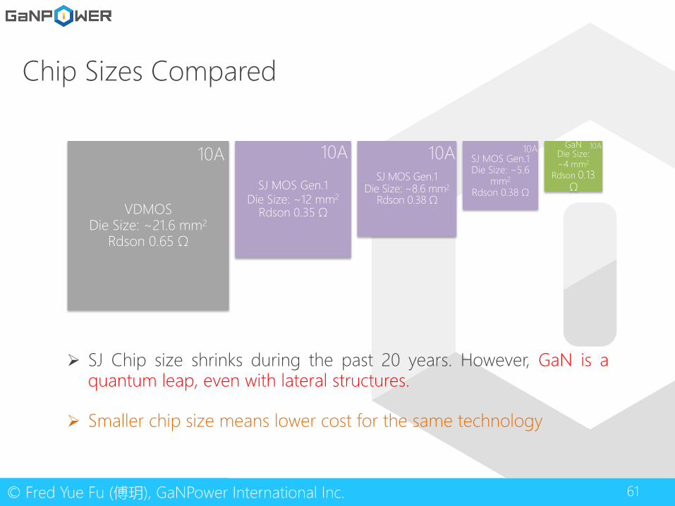
VDMOSDie Size: ~21.6 mm2
Rdson 0.65 Ω
SJ MOS Gen.1Die Size: ~12 mm2
Rdson 0.35 Ω
SJ MOS Gen.1Die Size: ~8.6 mm2
Rdson 0.38 Ω
SJ MOS Gen.1Die Size: ~5.6
mm2
Rdson 0.38 Ω
GaNDie Size: ~4 mm2
Rdson 0.13 Ω
Chip Sizes Compared
Ø SJ Chip size shrinks during the past 20 years. However, GaN is aquantum leap, even with lateral structures.
Ø Smaller chip size means lower cost for the same technology
10A 10A 10A 10A 10A
62© Fred Yue Fu (傅玥), GaNPower International Inc.
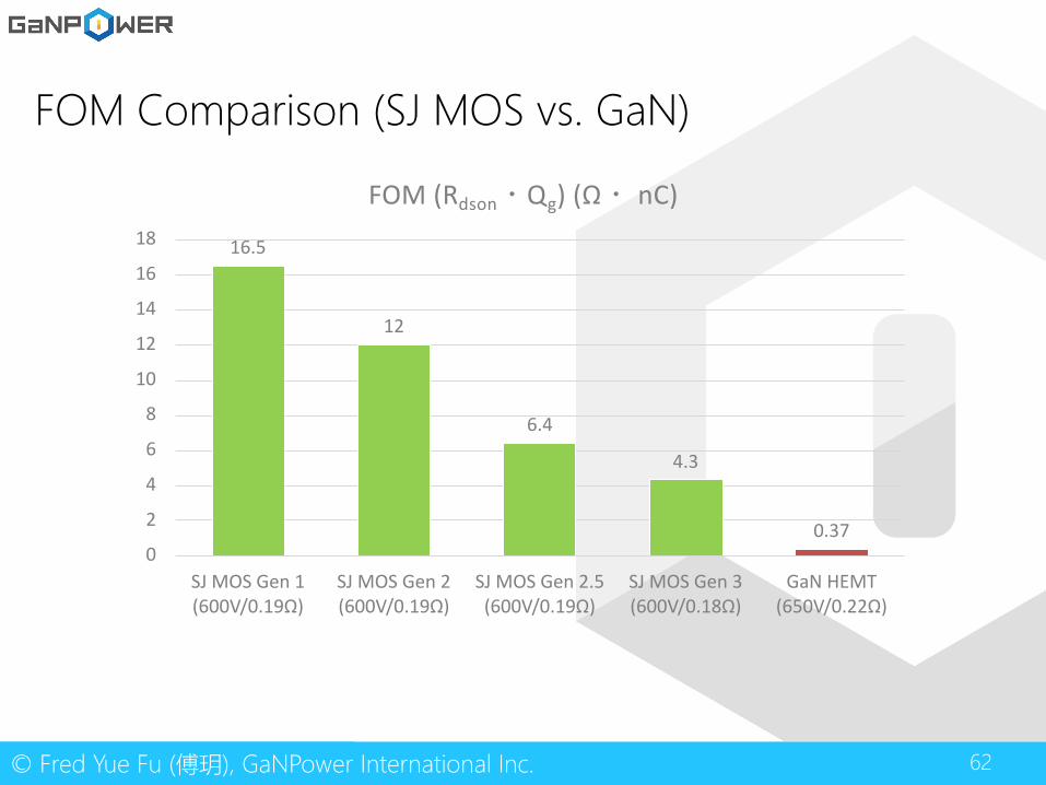
FOM Comparison (SJ MOS vs. GaN)
16.5
12
6.4
4.3
0.370
2
4
6
8
10
12
14
16
18
SJ MOS Gen 1 (600V/0.19Ω)
SJ MOS Gen 2 (600V/0.19Ω)
SJ MOS Gen 2.5 (600V/0.19Ω)
SJ MOS Gen 3 (600V/0.18Ω)
GaN HEMT (650V/0.22Ω)
FOM (Rdson・Qg) (Ω・ nC)
63© Fred Yue Fu (傅玥), GaNPower International Inc.
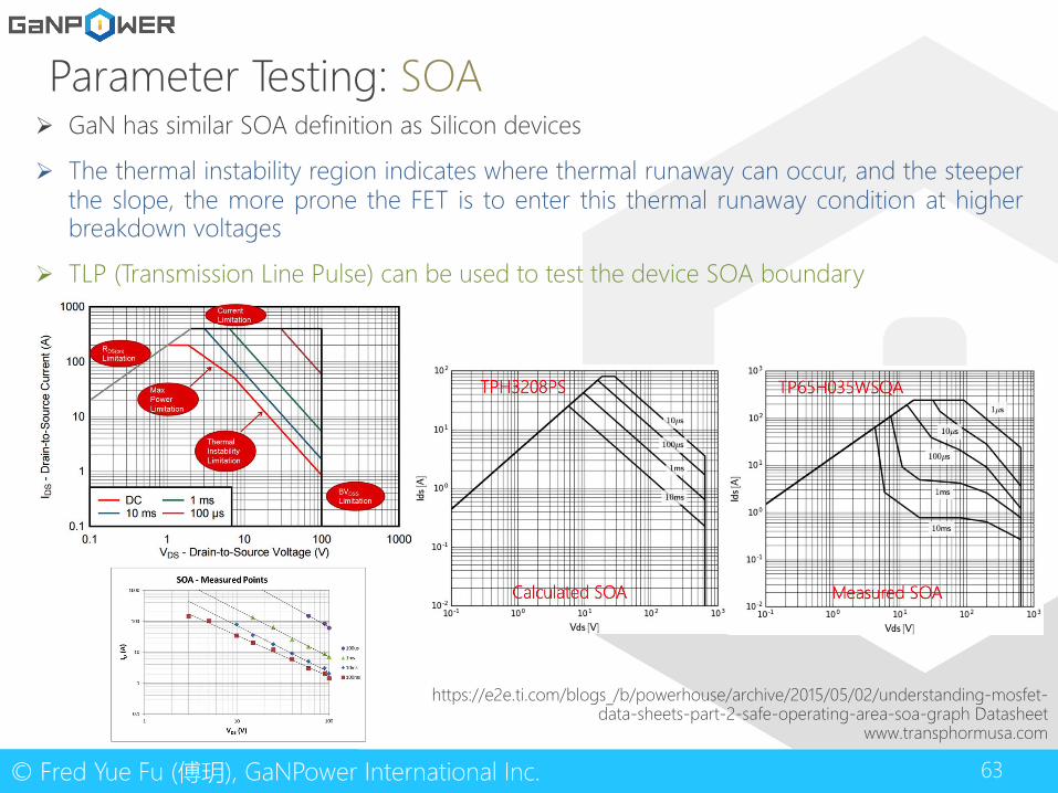
Parameter Testing: SOA
https://e2e.ti.com/blogs_/b/powerhouse/archive/2015/05/02/understanding-mosfet-data-sheets-part-2-safe-operating-area-soa-graph Datasheet
www.transphormusa.com
Ø GaN has similar SOA definition as Silicon devices
Ø The thermal instability region indicates where thermal runaway can occur, and the steeperthe slope, the more prone the FET is to enter this thermal runaway condition at higherbreakdown voltages
Ø TLP (Transmission Line Pulse) can be used to test the device SOA boundary
64© Fred Yue Fu (傅玥), GaNPower International Inc.
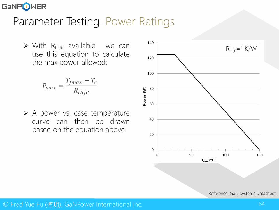
Ø With RthJC available, we canuse this equation to calculatethe max power allowed:
Ø A power vs. case temperaturecurve can then be drawnbased on the equation above
Parameter Testing: Power Ratings
𝑃E. =𝑇E. − 𝑇𝑅C
Reference: GaN Systems Datasheet
Rthjc=1 K/W
65© Fred Yue Fu (傅玥), GaNPower International Inc.
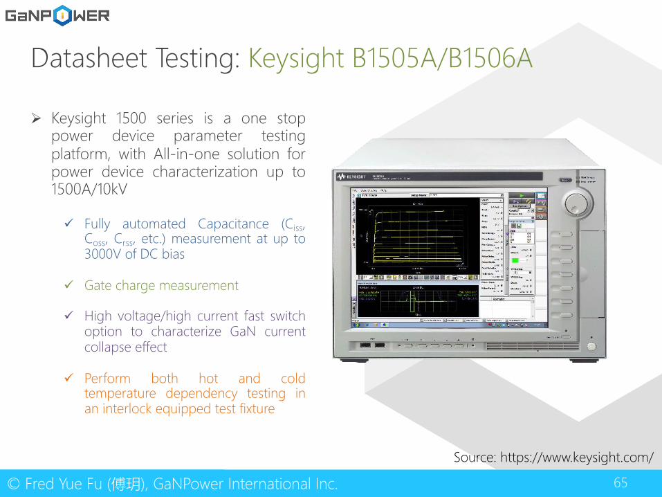
Datasheet Testing: Keysight B1505A/B1506A
Ø Keysight 1500 series is a one stoppower device parameter testingplatform, with All-in-one solution forpower device characterization up to1500A/10kV
ü Fully automated Capacitance (Ciss,Coss, Crss, etc.) measurement at up to3000V of DC bias
ü Gate charge measurement
ü High voltage/high current fast switchoption to characterize GaN currentcollapse effect
ü Perform both hot and coldtemperature dependency testing inan interlock equipped test fixture
Source: https://www.keysight.com/
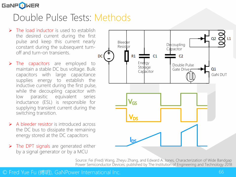
66© Fred Yue Fu (傅玥), GaNPower International Inc.
Bleeder Resistor
Energy Storage Capacitor
Decoupling Capacitor
Double Pulse Gate Drive
GaN DUT
Double Pulse Tests: Methods
VGS
VDS
IDS
Ø The load inductor is used to establishthe desired current during the firstpulse and keep this current nearlyconstant during the subsequent turn-off and turn-on transients.
Ø The capacitors are employed tomaintain a stable DC bus voltage. Bulkcapacitors with large capacitancesupplies energy to establish theinductive current during the first pulse,while the decoupling capacitor withlow parasitic equivalent seriesinductance (ESL) is responsible forsupplying transient current during theswitching transition.
Ø A bleeder resistor is introduced acrossthe DC bus to dissipate the remainingenergy stored at the DC capacitors
Ø The DPT signals are generated eitherby a signal generator or by a MCU
Source: Fei (Fred) Wang, Zheyu Zhang, and Edward A. Jones, Characterization of Wide Bandgap Power Semiconductor Devices; published by The Institution of Engineering and Technology 2018
67© Fred Yue Fu (傅玥), GaNPower International Inc.
Double Pulse Tests: Descriptions
Ø With a constant voltage and a given inductor in the test, there is a constantcurrent change rate di/dt during turn-on.
Ø The width of the first pulse is set to achieve the current you want to observe, fordevice characterization this often is the device's rated current.
Ø At the end of the first pulse, the double pulse test allows to observe "turn-offrated current".
Ø The current commutates to the freewheeling diode and gets back to the GaNwhen turning on the second pulse. An oscilloscope properly set will observe"turn-on of rated current" at the rising edge of the second pulse. However, duringthe turn-on period, the current in the device grows and does so exceeding therated current. As everything you want to learn takes place during the rising edge,the second pulse can be as short as possible.
Ø The important parts are the falling edge of pulse one and the rising edge ofpulse two.
http://athenaenergycorp.com/wp-content/uploads/2016/03/Rogowski_doublepulse_testing.pdf
68© Fred Yue Fu (傅玥), GaNPower International Inc.
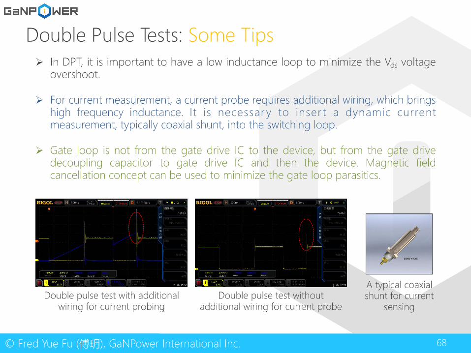
Double Pulse Tests: Some TipsØ In DPT, it is important to have a low inductance loop to minimize the Vds voltage
overshoot.
Ø For current measurement, a current probe requires additional wiring, which bringshigh frequency inductance. It is necessar y to inser t a dynamic currentmeasurement, typically coaxial shunt, into the switching loop.
Ø Gate loop is not from the gate drive IC to the device, but from the gate drivedecoupling capacitor to gate drive IC and then the device. Magnetic fieldcancellation concept can be used to minimize the gate loop parasitics.
Double pulse test with additional wiring for current probing
Double pulse test without additional wiring for current probe
A typical coaxial shunt for current
sensing

69© Fred Yue Fu (傅玥), GaNPower International Inc.
Contents
Ø Session 1: GaN devices basics
Ø GaN, An IntroductionØ GaN Design, Fabrication and TestingØ GaN Compact Modeling and Reliability
Ø Session 2: GaN Gate Driving
Ø Session 3: GaN Applications
70© Fred Yue Fu (傅玥), GaNPower International Inc.
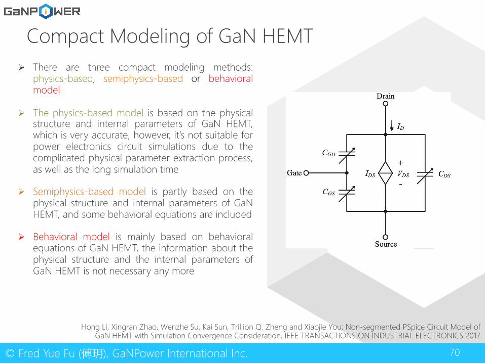
Compact Modeling of GaN HEMTØ There are three compact modeling methods:
physics-based, semiphysics-based or behavioralmodel
Ø The physics-based model is based on the physicalstructure and internal parameters of GaN HEMT,which is very accurate, however, it’s not suitable forpower electronics circuit simulations due to thecomplicated physical parameter extraction process,as well as the long simulation time
Ø Semiphysics-based model is partly based on thephysical structure and internal parameters of GaNHEMT, and some behavioral equations are included
Ø Behavioral model is mainly based on behavioralequations of GaN HEMT, the information about thephysical structure and the internal parameters ofGaN HEMT is not necessary any more
Hong Li, Xingran Zhao, Wenzhe Su, Kai Sun, Trillion Q. Zheng and Xiaojie You; Non-segmented PSpice Circuit Model of GaN HEMT with Simulation Convergence Consideration, IEEE TRANSACTIONS ON INDUSTRIAL ELECTRONICS 2017
71© Fred Yue Fu (傅玥), GaNPower International Inc.
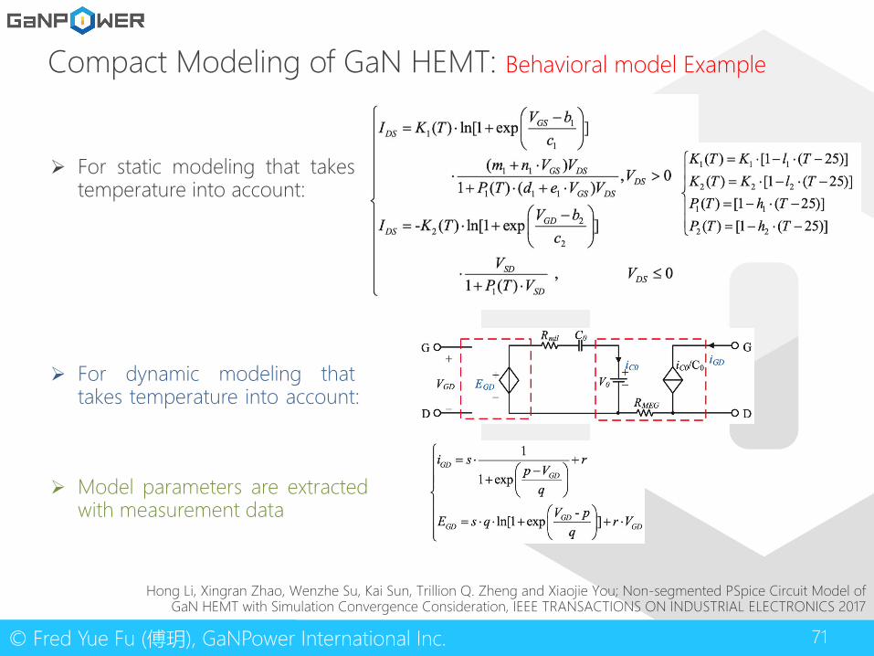
Compact Modeling of GaN HEMT: Behavioral model Example
Hong Li, Xingran Zhao, Wenzhe Su, Kai Sun, Trillion Q. Zheng and Xiaojie You; Non-segmented PSpice Circuit Model of GaN HEMT with Simulation Convergence Consideration, IEEE TRANSACTIONS ON INDUSTRIAL ELECTRONICS 2017
Ø For static modeling that takestemperature into account:
Ø For dynamic modeling thattakes temperature into account:
Ø Model parameters are extractedwith measurement data
72© Fred Yue Fu (傅玥), GaNPower International Inc.
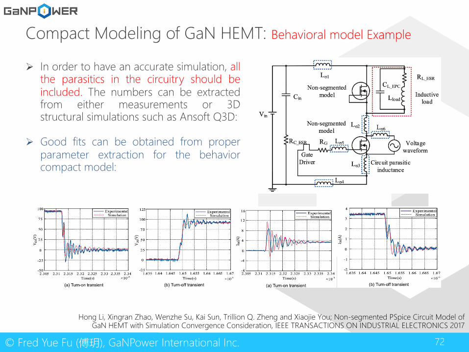
Compact Modeling of GaN HEMT: Behavioral model Example
Ø In order to have an accurate simulation, allthe parasitics in the circuitry should beincluded. The numbers can be extractedfrom either measurements or 3Dstructural simulations such as Ansoft Q3D:
Ø Good fits can be obtained from properparameter extraction for the behaviorcompact model:
Hong Li, Xingran Zhao, Wenzhe Su, Kai Sun, Trillion Q. Zheng and Xiaojie You; Non-segmented PSpice Circuit Model of GaN HEMT with Simulation Convergence Consideration, IEEE TRANSACTIONS ON INDUSTRIAL ELECTRONICS 2017
73© Fred Yue Fu (傅玥), GaNPower International Inc.
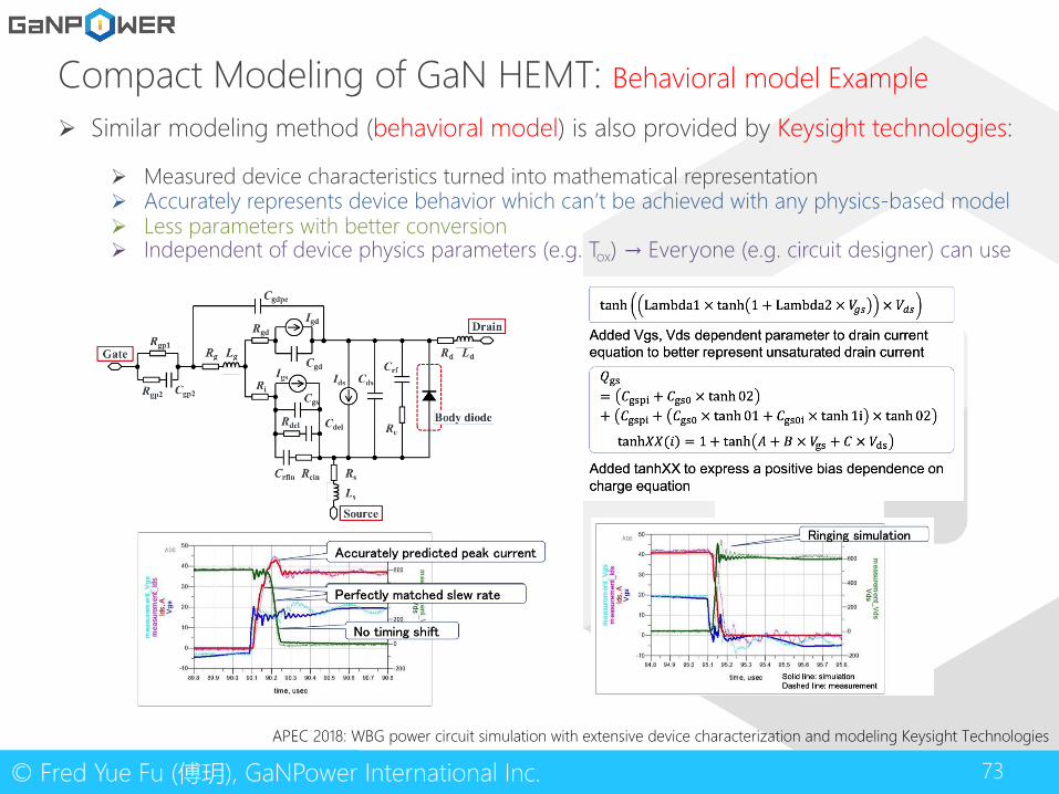
Ø Similar modeling method (behavioral model) is also provided by Keysight technologies:
Ø Measured device characteristics turned into mathematical representationØ Accurately represents device behavior which can’t be achieved with any physics-based modelØ Less parameters with better conversionØ Independent of device physics parameters (e.g. Tox) → Everyone (e.g. circuit designer) can use
APEC 2018: WBG power circuit simulation with extensive device characterization and modeling Keysight Technologies
Compact Modeling of GaN HEMT: Behavioral model Example
74© Fred Yue Fu (傅玥), GaNPower International Inc.
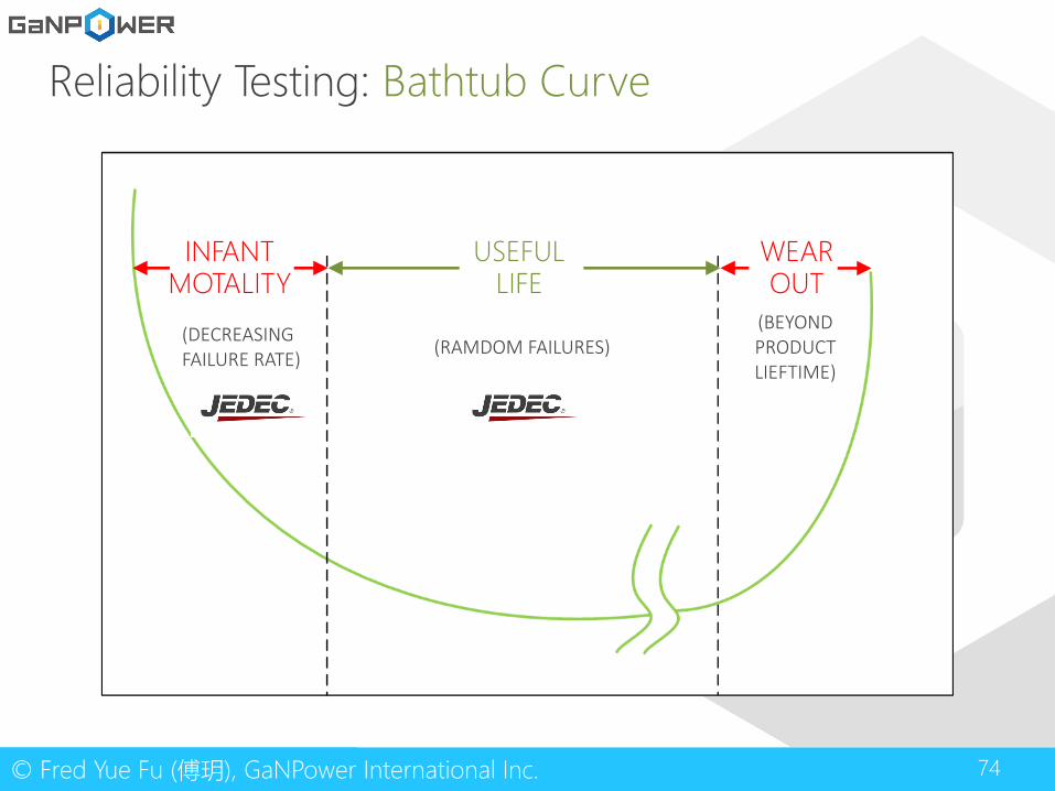
Reliability Testing: Bathtub Curve
INFANT MOTALITY
USEFUL LIFE
WEAROUT
(DECREASING FAILURE RATE) (RAMDOM FAILURES)
(BEYOND PRODUCT LIEFTIME)
75© Fred Yue Fu (傅玥), GaNPower International Inc.
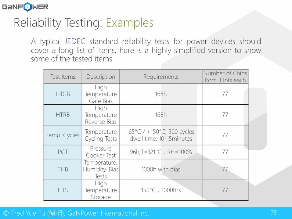
Reliability Testing: Examples
Test Items Description Requirements Number of Chipsfrom 3 lots each
HTGBHigh
Temperature Gate Bias
168h 77
HTRBHigh
Temperature Reverse Bias
168h 77
Temp. Cycles Temperature Cycling Tests
-65°C / +150°C, 500 cycles, dwell time: 10-15minutes 77
PCT Pressure Cooker Test 96h,T=121°C;RH=100% 77
THBTemperature, Humidity, Bias
Tests1000h with bias 77
HTSHigh
Temperature Storage
150°C,1000hrs 77
A typical JEDEC standard reliability tests for power devices shouldcover a long list of items, here is a highly simplified version to showsome of the tested items
76© Fred Yue Fu (傅玥), GaNPower International Inc.
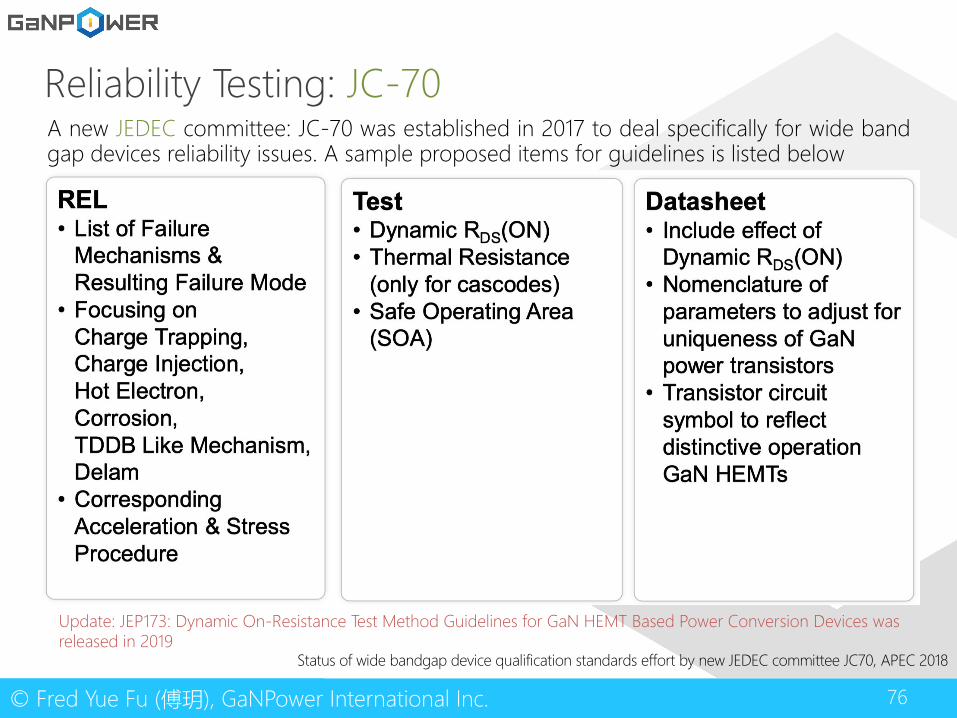
Reliability Testing: JC-70A new JEDEC committee: JC-70 was established in 2017 to deal specifically for wide bandgap devices reliability issues. A sample proposed items for guidelines is listed below
Status of wide bandgap device qualification standards effort by new JEDEC committee JC70, APEC 2018
Update: JEP173: Dynamic On-Resistance Test Method Guidelines for GaN HEMT Based Power Conversion Devices was released in 2019

77© Fred Yue Fu (傅玥), GaNPower International Inc.
ISO,RoHS and IATF16949
Ø ISO is the basic requirement forsemiconductor manufactures andpackaging houses.
Ø RoHS (Restriction of HazardousSubstances) is generally required.
Ø IATF16949 is one of the automotiveindustry’s most widely used internationalstandards for quality management
Ø For fabless design house such asGaNPower, we rely on our foundry andpackaging partners for these certificates
An example of RoHS test certificate

THANKS FOR WATCHING!
230-3410 LOUGHEED HWY VANCOUVER, BC, V5M 2A4 CANADALGA
1.778.588.1119
Contact us(Vancouver Headquarters):
中国江苏省苏州市工业园区纳米技术国家大学科技园F0411
+86-512-65267027
联系我们 ( Greater China Region )