g20 Cellular Engine Module Description - KORE...
48
Developer’s Guide 98-08901C66-O © Motorola Communications Ltd., 2003 A subsidiary of Motorola Inc. All rights reserved. g20 Cellular Engine Module Description
Transcript of g20 Cellular Engine Module Description - KORE...

Developer’s Guide98-08901C66-O
© Motorola Communications Ltd., 2003A subsidiary of Motorola Inc.All rights reserved.
g20 Cellular EngineModule Description
REVISION HISTORY
Revision Date Purpose

March 2003© Motorola Inc., 2003 98-08901C66-O
g20 Cellular EngineModule Description
CONTENTS REVISION HISTORY ................................................................................................................................................................ii
PREFACE1.1 SCOPE OF THIS MANUAL .................................................................................................................................................1
1.2 WHO SHOULD USE THIS MANUAL.................................................................................................................................1
1.3 APPLICABLE DOCUMENTS ..............................................................................................................................................11.3.1 Documents...................................................................................................................................................................11.3.2 Standards .....................................................................................................................................................................1
1.4 HOW THIS MANUAL IS ORGANIZED..............................................................................................................................1
INTRODUCTION2.1 GENERAL DESCRIPTION...................................................................................................................................................3
2.2 TERMS AND ABBREVIATIONS ........................................................................................................................................3
2.3 PRODUCT SPECIFICATIONS .............................................................................................................................................5
2.4 MODELS DESCRIPTION .....................................................................................................................................................7
2.5 REGULATORY APPROVALS .............................................................................................................................................7
2.6 REGULATORY STATEMENT.............................................................................................................................................7
2.7 SAFETY PRECAUTIONS.....................................................................................................................................................72.7.1 User Operation ............................................................................................................................................................72.7.2 Antenna Installation ....................................................................................................................................................8
HARDWARE DESCRIPTION3.1 G20 BLOCK DIAGRAM DESCRIPTION AND OPERATION OVERVIEW ....................................................................9
3.1.1 g20 Block Diagram .....................................................................................................................................................93.1.2 Basic RS232 and Analog Audio Connectivity..........................................................................................................113.1.3 Basic RS232 and Digital Audio Connectivity...........................................................................................................113.1.4 Additional Recommended Connections....................................................................................................................123.1.5 G20 for Handset Configuration.................................................................................................................................13
3.2 POWER SUPPLY AND CURRENT CONSUMPTION .....................................................................................................133.2.1 Power Supply Design ................................................................................................................................................133.2.2 G20 Current Consumption ........................................................................................................................................143.2.3 Turning the Unit On/Off ...........................................................................................................................................15

iv 98-08901C66-O
3.2.4 Sleep Mode Options ................................................................................................................................................. 16
3.3 COMMUNICATION INTERFACES.................................................................................................................................. 183.3.1 RS232 ....................................................................................................................................................................... 183.3.2 USB .......................................................................................................................................................................... 203.3.3 SIM ........................................................................................................................................................................... 213.3.4 SPI ............................................................................................................................................................................ 223.3.5 Unique g20 Interfaces............................................................................................................................................... 22
3.4 AUDIO INTERFACES........................................................................................................................................................ 233.4.1 Analog Audio Interfaces........................................................................................................................................... 233.4.2 Digital Audio Interface ............................................................................................................................................. 27
3.5 ANTENNA........................................................................................................................................................................... 283.5.1 Antenna Performance Recommendations ................................................................................................................ 28
3.6 CHARGER INTERFACE.................................................................................................................................................... 28
3.7 DISPLAY INTERFACE ...................................................................................................................................................... 28
3.8 ESD PROTECTION ............................................................................................................................................................ 29
CONNECTOR PIN ASSIGNMENTS4.1 CONNECTORS ................................................................................................................................................................... 31
4.2 PIN ASSIGNMENTS .......................................................................................................................................................... 31
MECHANICAL DESCRIPTION5.1 MECHANICAL DETAILS.................................................................................................................................................. 37
SERVICE SUPPORT6.1 CUSTOMER ASSISTANCE............................................................................................................................................... 39
6.2 TESTING A STANDALONE UNIT................................................................................................................................... 39
6.3 TROUBLESHOOTING ....................................................................................................................................................... 39
6.4 PROGRAMMING ............................................................................................................................................................... 39
INDEX
98-08901C66-O v
LIST OF FIGURESFigure 1. g20 Block Diagram .......................................................................................................................................................9
Figure 2. Basic RS232 and Analog Audio Connectivity ............................................................................................................11
Figure 3. Basic RS232 and Digital Audio Connectivity.............................................................................................................12
Figure 4. Additional g20 Connectivity .......................................................................................................................................12
Figure 5. g20 for Handset Configuration....................................................................................................................................13
Figure 6. VCC Signal During TX Periods ..................................................................................................................................14
Figure 7. On/Off Signal Timing Diagram ..................................................................................................................................15
Figure 8. CTS Sleep Mode Timing.............................................................................................................................................16
Figure 9. DCE/DTE Connectivity ..............................................................................................................................................17
Figure 10. Waking Up the g20 when the DTE Wants to Send Data ..........................................................................................17
Figure 11. Waking Up the DTE when the g20 Wants to Send Data ..........................................................................................18
Figure 12. g20 RS232 Interface ..................................................................................................................................................18
Figure 13. RS232 Connection.....................................................................................................................................................19
Figure 14. g20 USB Connection for g20 Models with a USB Driver ........................................................................................20
Figure 15. g20 USB Connection for g20 Models without a USB Driver ...................................................................................21
Figure 16. g20 SIM Connection .................................................................................................................................................21
Figure 17. TX_EN Transmission................................................................................................................................................22
Figure 18. Antenna-detect Circuit ..............................................................................................................................................23
Figure 19. GPRS-detect Coverage Indication.............................................................................................................................23
Figure 20. SPKR_N Output Configuration.................................................................................................................................24
Figure 21. Mechanical Mounting Requirements ........................................................................................................................37

vi 98-08901C66-O
LIST OF TABLESTable 1. Terms and Abbreviations ............................................................................................................................................... 3
Table 2. Product Specifications.................................................................................................................................................... 5
Table 3. g20 Models..................................................................................................................................................................... 7
Table 4. g20 Current Consumption ............................................................................................................................................ 14
Table 5. SPI Pinout..................................................................................................................................................................... 22
Table 6. SPKR_N Output when g20 Set to Maximum Volume Level and Headset Interrupt is Low....................................... 24
Table 7. SPKR_N Output when g20 Set to Maximum Volume Level and Headset Interrupt is Not Low................................ 25
Table 8. SPKR_N Output when a 500mV RMS Signal is Transmitted..................................................................................... 25
Table 9. SPKR_N Output when g20 is in Handset Mode.......................................................................................................... 26
Table 10. SPKR_N Output when g20 is in Headset Mode ........................................................................................................ 26
Table 11. Alert Transducer Levels for the ALERT_P Signal .................................................................................................... 27
Table 12. Antenna Performance Recommendations .................................................................................................................. 28
Table 13. g20 Interface Connector Pin Assignments ................................................................................................................. 31

98-08901C64-O 1
1. PREFACE
1.1 SCOPE OF THIS MANUAL
This manual introduces the g20 embedded module and describes the technical details required by the data terminal equipment(DTE) team to successfully integrate the Motorola g20 cellular engine into an original equipment manufacturer (OEM) wirelesshost device.
We at Motorola want to make this guide as helpful as possible. Keep us informed of your comments and suggestions forimprovements.
You can reach us by Email at: GSM [email protected].
1.2 WHO SHOULD USE THIS MANUAL
This manual is intended for all members of the DTE OEM integration team who are responsible for integrating the c18 moduleinto the host OEM device, including representatives from hardware, software and RF engineering disciplines.
1.3 APPLICABLE DOCUMENTS
PLEASE PROVIDE DETAILS FOR THIS SECTION.
1.3.1 Documents
g20 Developer’s Kit - 9808901C67-O
g20 AT Commands - 9808901C68-O
1.3.2 Standards
PLEASE PROVIDE DETAILS FOR THIS SECTION.
1.4 HOW THIS MANUAL IS ORGANIZED
This manual contains the following chapters:
• Chapter 1 contains this Preface.
• Chapter 2 introduces the g20 unit and provides important safety instructions.
• Chapter 3 provides a detailed hardware description of the blocks and components comprising the g20.
• Chapter 4 describes the pin assignments for g20 connectors.
• Chapter 5 describes mechanical requirements for the g20 unit.
• Chapter 6 provides contact information for Motorola Service Support and Customer Assistance, as well as valuabletroubleshooting and programming information.

Preface
2 98-08901C64-O

98-08901C64-O 3
2. INTRODUCTION
2.1 GENERAL DESCRIPTION
The g20 is Motorola’s newest family of embedded cellular products. Motorola continues its tradition of excellence byintroducing this new cellular engine family for GSM/GPRS communications, consisting of the d10, the d15 and the g18.
The new module is similar to a condensed cellular phone core, and can be integrated in any system or product that needs totransfer voice or data information. Thus, it significantly enhances the system’s capabilities, transforming it from a standalone,isolated product to a powerful component connected to communication nets.
The new g20 is extremely small in dimensions, yet packed with a host of highly-advanced features designed to facilitate fastand easy integration with OEM user products. It significantly shortens the development process for OEM developers, thanks toits wide range of built-in applications, and minimizes the product’s time to market.
The g20 module is ideally suited for the automotive, telemetry, security, insurance and EPOS industries, for delivery andhandheld terminals, and for PDA markets.
2.2 TERMS AND ABBREVIATIONS
This section provides definitions for terms and acronyms used in this document.
Table 1. Terms and Abbreviations
Acronym/Term Definition/Description
AOC Automatic Output Control
BABT British Approval Board - Telecommunications
CSD Circuit-switched Data
DCE Data Communication Equipment (such as modems)
DCS Digital Cellular System (GSM in the 1800MHz band)
DOC Department of Communications (Canada)
DSP Digital Signal Processor
DTE Data Terminal Equipment (such as terminals, PCs and so on)
DTMF Dual-Tone Multi-Frequency
EGSM Extended Global System for Mobile Communications
EIRP Effective Isotropic Radiated Power
EMC WHAT DOES THIS STAND FOR?
EOTD Enhanced Observed Time Difference
EPOS Electronic Point of Sale
ERP Effective Radiated Power
ESD Electrostatic Discharge
FCC Federal Communications Commission (U.S.)
FTA Foreign Telecommunication Administration

Introduction
4 98-08901C64-O
GCF WHAT DOES THIS STAND FOR?
GPIO General Purpose Input/Output
GPRS General Packet Radio Service
GSM Global System for Mobile Communications
IC Integrated Circuit
LNA Low-noise Amplifier
MMCX Multimedia Communications Exchange
MO Mobile Originated
MT Mobile Terminated
OEM Original Equipment Manufacturer
PCB Printed Circuit Board
PCM Pulse Code Modulation
PCS Personal Communication System (also known as CDMA 1900)
PDA Personal Data Assistant
PDU Packet Data Unit
PLL Phase-locked Loop
PTCRB PCS-1900 Type Certification Review Board (GSM North America)
R&TTE Radio and Telecommunications Terminal Equipment
RMS Root Mean Square
RTS Request To Send
SAR Segmentation and Reassembly
SIM Subscriber Identity Module
SMS Short Message Service
SPI Serial Peripheral Interface
TDMA Time Division Multiple Access
UART Universal Asynchronous Receiver Transmitter
USB Universal Serial Bus
USSD Unstructured Supplementary Services Data
VCC Voltage Common Collector
VSWR Voltage Standing Wave Ratio
Table 1. Terms and Abbreviations (Continued)
Acronym/Term Definition/Description

98-08901C64-O 5
Introduction
2.3 PRODUCT SPECIFICATIONS
Table 2. Product Specifications
Product Features
Operating systems: EGSM: 900/1800 MHzGSM: 850/1900 MHz
Physical Characteristics
Size: Size: 24.4 x 48.2 x 6.0 mm
Mounting: Two 2.2 mm holes
Weight: 11.9 grams
Environmental
Operational temperature: -20°C +60°C
Functional temperature: -20°C +70°C
Storage temperature: -40°C +85°C
Performance
Operating voltage: Voltage: 3.0 - 4.2 V
Current consumption: < 2.5 mA @ DRX9 (Idle mode)
Tx power: • 0.6 W, 850 MHz• 2 W, 900 MHz
• 1 W, 1800/1900 MHz
Interfaces
Connectors: • Single 70-pin, board-to-board• RF MMCX
SIM Card: • Local SIM connectivity• 32K SIM
• 1.8/3.0 V
Serial: • RS232:• BR from 300 bps to 115 Kbps• Auto BR from 300 bps to 115 Kbps
• USB• 12 Mbps USB specifications, Rev. 1.1
Data Features
GPRS: • Multi-slot class 8 (4 down; 1 up)• Max BR 85.6 Kbps
• Class B GSM 07.10 multiplexing protocol• Coding scheme CS1-CS4
CSD: Max BR 14.4 Kbps
SMS: • MO/MT Text and PDU modes
• Cell broadcast
FAX Class 1
Voice Features
Telephony
Digital audio
Differential analog audio lines

Introduction
6 98-08901C64-O
Voice Features (Continued)
Vocoders EFR/ER/FR/AMR
DTMF support
Audio control: echo cancellation, noise suppression, side tone and gain control
GSM Supplementary Service
USSD Phase II
Call forwarding
Call hold, waiting and multiparty
Call diverting
Missed-call indicator
AOC
Call barring
Character Set
UTF8
UCS2
Control/Status Indicators
GPRS coverage
Wakeup
Antenna detect
TX enable
Reset
Entertainment mute
Features over RS232
Embedded TCP/IP stack
STK Class II
User Application
Application Programming Interface (API)
12 GPIO lines
2 A/D lines
Emergency and Location
FCC E911 Phase II Location Mandate using EOTD
AT Command Set
GSM 07.05
GSM 07.07
Motorola proprietary AT commands
Accessories
Firmware data loader
Data logger
Developer Kit
Note
Specifications are subject to change without prior notice.
Table 2. Product Specifications (Continued)
98-08901C64-O 7
Introduction
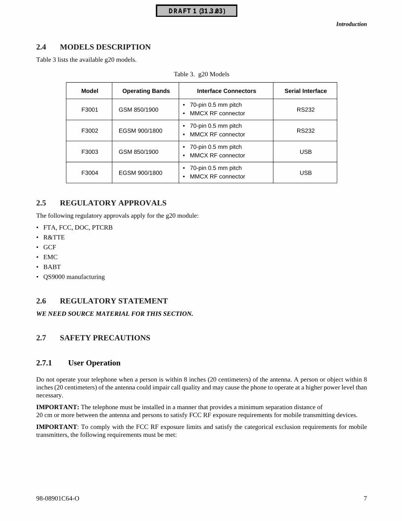
2.4 MODELS DESCRIPTION
Table 3 lists the available g20 models.
2.5 REGULATORY APPROVALS
The following regulatory approvals apply for the g20 module:
• FTA, FCC, DOC, PTCRB
• R&TTE
• GCF
• EMC
• BABT
• QS9000 manufacturing
2.6 REGULATORY STATEMENT
WE NEED SOURCE MATERIAL FOR THIS SECTION.
2.7 SAFETY PRECAUTIONS
2.7.1 User Operation
Do not operate your telephone when a person is within 8 inches (20 centimeters) of the antenna. A person or object within 8inches (20 centimeters) of the antenna could impair call quality and may cause the phone to operate at a higher power level thannecessary.
IMPORTANT: The telephone must be installed in a manner that provides a minimum separation distance of 20 cm or more between the antenna and persons to satisfy FCC RF exposure requirements for mobile transmitting devices.
IMPORTANT: To comply with the FCC RF exposure limits and satisfy the categorical exclusion requirements for mobiletransmitters, the following requirements must be met:
Table 3. g20 Models
Model Operating Bands Interface Connectors Serial Interface
F3001 GSM 850/1900• 70-pin 0.5 mm pitch• MMCX RF connector
RS232
F3002 EGSM 900/1800• 70-pin 0.5 mm pitch
• MMCX RF connectorRS232
F3003 GSM 850/1900• 70-pin 0.5 mm pitch• MMCX RF connector
USB
F3004 EGSM 900/1800• 70-pin 0.5 mm pitch• MMCX RF connector
USB

Introduction
8 98-08901C64-O
2.7.2 Antenna Installation
• A minimum separation distance of 20 cm needs to be maintained between the antenna and all persons, otherwise a SAR testwill be required.
• The transmitter effective radiated power must be less than 1.5 Watts ERP (2.45 Watts or 33.9 dBm EIRP). This requires thatthe combination of antenna gain and feed line loss does not exceed 11 dBi.

98-08901C64-O 9
3. HARDWARE DESCRIPTION
3.1 G20 BLOCK DIAGRAM DESCRIPTION AND OPERATION OVERVIEW
This chapter describes the basic blocks comprising the g20 module and the connectivity options for the module.
3.1.1 g20 Block Diagram
Figure 1 shows a block diagram for the g20 module:
Figure 1. g20 Block Diagram
The g20 consists of the following blocks:
• Power and Audio Management IC: This block is responsible for the power on/off process, analog audio drivers, internalregulators, realtime clock activities, and the battery charging process. When an On command is received, this IC wakes upthe internal regulators and controls the reset process. This activity turns the unit on. When an Off command is received, thisIC sends the request to the main processor, which in turn shuts down the unit in an orderly fashion. During shutdown, theunit is disconnected from the network, all tasks are terminated and the regulators are shut down. The on/off inputs (On/Offand Ignition) are always on, even when the unit is off.
TransmitterIC
MainProcessor
&DSP
Memories
Power & AudioManagement IC
ReceiverIC
Control
Serial
USBDriver
PCM
SIM
GPIO
SPI
ADC
Audio
Charger
Power
Inte
rfac
e C
onne
ctor
G20
Ant
On/Off / IGN
Hardware Description
10 98-08901C64-O
• Main Processor and DSP: This block is responsible for all the main tasks in the unit. This block contains the followingcomponents:
• Main processor
• DSP for controlling speech options
• UART
• USB block
• Digital audio driver
• SIM card
• Two SPI buses (one internal and one externally accessible)
• Main clock (26 MHz)
• Address/data buses
• RF PLL
• Controller to the RF ICs, which is the heart of the unit
This module provides the following connectivity:
• Address/data bus
• UART to the user connector
• USB via an optional USB driver to the user connector
• Digital audio (PCM) to the user connector
• SIM card interface
• SPI to the user connector
• SPI to control the RF ICs
• Control signals to the power amplifier IC
• Handshake with the Power and Audio Management IC
• General I/O to the user connector
• Receiver Block: This block is an RF block that contains all the receiver channels. It contains the following components:
• Front filters
• LNAs
• Mixers
• VCOs
• I/Q outputs
• Control signals
• Transmitter Block: This is an RF block that contains all the transmitter channels. It contains the following components:
• Power amplifiers
• Power control loop
• Antenna switch
• Harmonic filter
• Input buffers
• Control signals
• Antenna connection
98-08901C64-O 11
Hardware Description
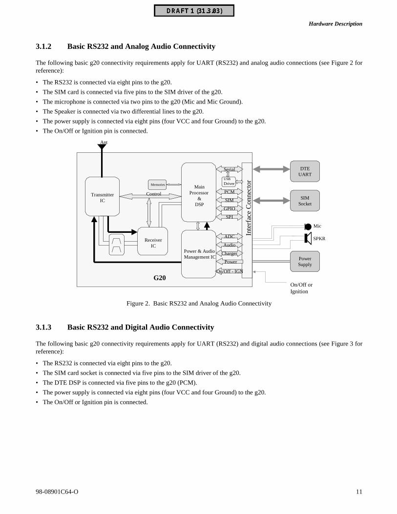
3.1.2 Basic RS232 and Analog Audio Connectivity
The following basic g20 connectivity requirements apply for UART (RS232) and analog audio connections (see Figure 2 forreference):
• The RS232 is connected via eight pins to the g20.
• The SIM card is connected via five pins to the SIM driver of the g20.
• The microphone is connected via two pins to the g20 (Mic and Mic Ground).
• The Speaker is connected via two differential lines to the g20.
• The power supply is connected via eight pins (four VCC and four Ground) to the g20.
• The On/Off or Ignition pin is connected.
Figure 2. Basic RS232 and Analog Audio Connectivity
3.1.3 Basic RS232 and Digital Audio Connectivity
The following basic g20 connectivity requirements apply for UART (RS232) and digital audio connections (see Figure 3 forreference):
• The RS232 is connected via eight pins to the g20.
• The SIM card socket is connected via five pins to the SIM driver of the g20.
• The DTE DSP is connected via five pins to the g20 (PCM).
• The power supply is connected via eight pins (four VCC and four Ground) to the g20.
• The On/Off or Ignition pin is connected.
DTEUART
SIMSocket
TransmitterIC
MainProcessor
&DSP
Memories
Power & AudioManagement IC
ReceiverIC
Control
Serial
USBDriver
PCM
SIM
GPIO
SPI
ADC
Audio
Charger
Power
Inte
rfac
e C
onne
ctor
G20
Ant
PowerSupply
Mic
SPKR
On/Off orIgnition
On/Off - IGN

Hardware Description
12 98-08901C64-O
Figure 3. Basic RS232 and Digital Audio Connectivity
3.1.4 Additional Recommended Connections
Additional g20 connectivity options are described below (see Figure 4 for reference):
• A USB connector that is connected via three lines to the g20. In this case, when USB is used, the DTE UART should be intri-state (high impedance).
• A USB connector that is connected via a USB driver to the g20 (in g20 models without a USB driver). When USB is used,the DTE UART should be in tri-state (high impedance).
• An SPI block that is connected via four pins to the g20 (for debug accessibility).
Figure 4. Additional g20 Connectivity
TransmitterIC
MainProcessor
&DSP
Memories
Power & AudioManagement IC
ReceiverIC
Control
Serial
USBDriver
PCM
SIM
GPIO
SPI
ADC
Audio
Charger
Power
Inte
rfac
e C
onne
ctor
G20
DTEUART
SIMSocket
Ant
PowerSupply
DTEDSP
On/Off / IGNOn/Off or IGN
TransmitterIC
MainProcessor
&DSP
Memories
Power & AudioManagement IC
ReceiverIC
Control
Serial
USBDriver
PCM
SIM
GPIO
SPI
ADC
Audio
Charger
Power
Inte
rfac
e C
onne
ctor
G20
USBDriver
Ant
USBConnector
SPIDevice

98-08901C64-O 13
Hardware Description
3.1.5 G20 for Handset Configuration
g20 connectivity when using the g20 as a cellular phone engine is described below (see Figure 5 for reference):
• The display is connected via five pins to the g20.
• The keypad is connected via eight pins to the g20.
• The SIM card socket is connected via five pins to the g20 SIM driver.
• The charger is connected via six pins (Interface to National LM3652) to the g20.
• The microphone is connected via two pins (Mic and Mic Ground) to the g20.
• The speaker is connected via two differential lines to the g20.
• The alert device is connected via two differential lines to the g20.
• The vibrator is connected via one pin to the g20.
• The battery is connected to the charger, and the charger is connected to the VCC and Ground pins.
Figure 5. g20 for Handset Configuration
3.2 POWER SUPPLY AND CURRENT CONSUMPTION
This section describes the following power-related considerations for the g20:
• Power supply design
• g20 current consumption
• Turning the unit on/off
• Sleep mode options
3.2.1 Power Supply Design
The following power supply design considerations apply to the g20:
• The g20 is designed to operate between 3.0 V to 4.2 V on the g20 input (after all losses). In order to reduce battery powerconsumption, it is important to verify power supply line and regulator losses in the PCB.
• The g20 is a GSM/GPRS phone that transmits in 0.5 ms pulses every 4.6 ms. The peak current is approximately 2.0 A.
TransmitterIC
MainProcessor
&DSP
Memories
Power & AudioManagement ICReceiver
IC
Control
Display
SIM
Audio
Charger
Power
Inte
rfac
e C
onne
ctor
G20
Display
SIMSocket
Ant
Battery
Mic
SPKR
Key Pad
Alert
VibratorAlert
Vibrator
Key Pad
Charger

Hardware Description
14 98-08901C64-O
• When the power supply is lower than 2.85 V, the g20 software determines that the battery is low and disconnects the unit.
• When the voltage is greater than 4.25 V, the g20 software detects an over voltage condition and does not allow the unit toestablish a call.
• The VCC line typically drops during TX periods.
Figure 6. VCC Signal During TX Periods
To minimize the ∆, it is recommended to use lines that are as short as possible, and to place a 1000uF capacitor (or the maximumpossible) in the g20 VCC input. (When a battery is used, there is no need for a large capacitor.)
It is recommended to keep the ∆ less than 0.3 V.
3.2.1.1 Power Supply RF Filtering
It is recommended to add RF filtering to the DC lines.
Use 100nF, 39pF, 22pF or 8.2pF capacitors in parallel to the power supply lines (close to the g20 connector). MUST ALLTHESE CAPACITORS BE USED IN PARALLEL? OR SOME COMBINATION?
3.2.2 G20 Current Consumption
In order to design the power supply correctly and to calculate the battery life, you should take into account the currentconsumption of the g20 when operating in different modes.
Note
The power supply should be able to drive at least 2.5 A.
Table 4. g20 Current Consumption
Mode Current Consumption (mA RMS)
g20 in Sleep mode (camped and Sleep-mode enabled)
< 2.5 mA, RMS @ DRX9, Typical 2.2 mA
< 4.5 mA, RMS @ DRX2, Typical 3.5 mA
g20 during search time < 40 mA, RMS, Typical 25 mA, RMS
g20 off < 100 uA – Typical 25 uA
g20 during a call
GSM 900 @ Power level #5 < 350 mA, Typical 270 mA
@ Power level #10, Typical 160 mA@ Power level #19, Typical 135 mA
TX TX TXTransmit Periods
VCC
98-08901C64-O 15
Hardware Description
3.2.3 Turning the Unit On/Off
Two different mechanisms are available to turn the g20 on and off:
• On/Off signal (Pin 53)
• Ignition line (Pin 51)
3.2.3.1 On/Off Signal
After power is applied to the g20, the on/off signal is pulled high to the VCC by a 200kΩ resistor.
To turn the g20 on, the on/off signal should be pulled low for a minimum of 700 ms.
After the g20 is turned on, the line should be pulled low for a minimum of 1.1 seconds to turn it off. The unit can be turned offonly if at least seven seconds have elapsed since turning it on.
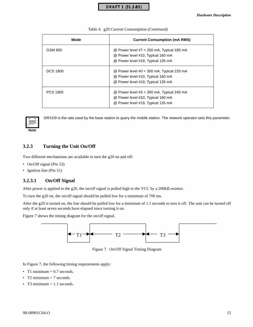
Figure 7 shows the timing diagram for the on/off signal.
Figure 7. On/Off Signal Timing Diagram
In Figure 7, the following timing requirements apply:
• T1 minimum = 0.7 seconds.
• T2 minimum = 7 seconds.
• T3 minimum = 1.1 seconds.
GSM 850 @ Power level #7 < 250 mA, Typical 185 mA@ Power level #10, Typical 160 mA
@ Power level #19, Typical 135 mA
DCS 1800 @ Power level #0 < 300 mA, Typical 220 mA@ Power level #10, Typical 160 mA
@ Power level #19, Typical 135 mA
PCS 1900 @ Power level #5 < 300 mA, Typical 240 mA@ Power level #10, Typical 160 mA
@ Power level #19, Typical 135 mA
Note
DRX2/9 is the rate used by the base station to query the mobile station. The network operator sets this parameter.
Table 4. g20 Current Consumption (Continued)
Mode Current Consumption (mA RMS)
T1 T2 T3

Hardware Description
16 98-08901C64-O
3.2.3.2 Ignition Line
When the g20 ignition line is held at a high level, the g20 is turned on. When this line is pulled low, the g20 is turned off. Inorder to protect the line from voltage bounces, the g20 is tuned off only if the line is held low for at least 500 ms.
The high input to the ignition line must be greater than 2.75 V. The line can tolerate up to 40 V.
After the g20 is turned on, the application should wait for DSR before sending data to the g20. The DSR becomes active loweight seconds after the start of T1, or after the ignition line is pulled high. DSR is only valid with UART, and is not valid withUSB.
3.2.4 Sleep Mode Options
This section describes how the g20 can be awakened by the DTE and vice-versa.
The DCE (g20) and the DTE can incorporate a sleep mechanism in their application in order to conserve battery life.
Sleep mode enables the g20 to be awakened when the DTE wants to communicate with it. Conversely, it also enables the DTEto be awakened by the g20 when the g20 wants to communicate with it.
3.2.4.1 General
• The g20 Sleep Mode option can be enabled or disabled using ATS24.
• Sleep mode is activated by sending ATS24 = n, where n = 1, 2, 3 or 4 seconds. (To disable Sleep mode, send ATS24=0.)
• The g20 drops the CTS (h/w Flow Control) when it is in Sleep mode.
• The g20 does not enter Sleep mode when data is present on TXD or RXD lines.
• At the end of the TXD (meaning, the TXD buffer is empty), the g20 waits n seconds (as defined in ATS24 = n) before enter-ing Sleep mode.
• The DTE uses CTS to send data only when the g20 is awake. The DTE waits when the g20 is in Sleep mode.
• The DTE should drop RTS during the sleep period in order to prevent the loss of data sent by the g20.
Figure 8. CTS Sleep Mode Timing

98-08901C64-O 17
Hardware Description
3.2.4.2 DCE/DTE Connectivity
Figure 9 shows DCE/DTE connectivity:
Figure 9. DCE/DTE Connectivity
Waking Up the DCE:
The following apply when waking up the DCE:
• The Wake-up In line is used to awaken the g20. This input is routed into an Interrupt in the g20.
• Whenever the Wake-up In line is at logic “low”, the g20 remains in an awake state.
• When the DTE needs to send data, it should activate this line, wait 30 ms (the wake time required for the g20), and then startsending the data.
• While the DTE is sending data, the wake-up line should remain low, so that the g20 does not enter Sleep mode.
Figure 10. Waking Up the g20 when the DTE Wants to Send Data
Waking Up the DTE:
The following apply when waking up the DTE:
• The g20 uses the Wake-up Out line to indicate to the DTE that data is present.
• The DTE should not enter Sleep mode when the Wake-up Out line is low.
• When the g20 has data to send to the DTE, it drops the Wake-up Out line to low.
• The g20 will send the Wake-up Out line #ms to low, as indicated by S10x in Figure 11.
DTE TXD
Wake up In line
30 ms 30 ms 30 ms

Hardware Description
18 98-08901C64-O
• While the g20 is sending data, the Wake-up Out line remains low.
• After the sending of data is completed, the g20 brings the Wake-up Out line to high.
• The DTE should keep RTS off during this sleep period in order to avoid sending data when it is not ready.
Figure 11. Waking Up the DTE when the g20 Wants to Send Data
3.3 COMMUNICATION INTERFACES
This section describes the following four interfaces that are available in the g20:
• RS232
• USB
• SIM
• SPI
3.3.1 RS232
The following apply when usingthe RS2332 interface of the g20:
• The g20 supports full hard-ware flow control (9 pins),software flow control (Xon/Xoff) and non-flow control.
• The g20 UART is connected directly to the interface connector.
• The g20 is a DCE device. Applicable line terminology is shown in Figure 12.
Figure 12. g20 RS232 Interface
RXD
Wake up Out line
S10x ms S10x ms S10x ms

98-08901C64-O 19
Hardware Description
3.3.1.1 RS232 Levels
RS232 levels are as follows:
• Vih = 1.95 V minimum, 3.0 V maximum
• Vil = 0.8 V maximum
• Voh = 2.56 V minimum @ 100 uA
• Vol = 0.2 V maximum @ 100 uA
3.3.1.2 RS232 Connection
Figure 13 shows an RS232 connection diagram:
Figure 13. RS232 Connection
The following apply for g20 RS232 connections:
• The g20 can use both UART and USB connectors, but cannot use them both simultaneously.
• When USB is detected (by sensing the USB VBUS signal), the UART is disconnected from the g20 main processor pins andUSB functionality is added instead.
• The DTE should unload the RS232 lines when USB is used in order for the USB to function properly.
• RS232 signals are routed directly from the main processor to the connector.
Note
A buffer is required whenever DTE levels do not match g20 levels.
Note
In g20 models without a USB driver (F3001and F3002 models), RS232 signals can be used to connect an externalUSB driver.
G20 MainProcessor
UART
USB
MUX
USBDriver
D+
D-
USB VBUSUSBDetect
TXD21
RXD11
RTS
CTS
DTR
DSR
DCD
RI
9
15
19
13
17
23
12
14
10
DTE
UART
USB connector
3 state
G20 DTE

Hardware Description
20 98-08901C64-O
3.3.2 USB
The following apply for g20 USB connections:
• The g20 can use a USB port to communicate with a DTE device.
• The USB port is also used to load software into the g20. It is recommended to include connectivity to this port in the userapplication.
• The g20 supports USB1.1 at a baud rate of 12 Mbps.
• The g20 supports two basic types, one with a USB driver (models F3003 and F3004), and one with the USB driver removed(models F3001 and F3002).
3.3.2.1 USB Connection
Figure 14 shows g20 connection for g20 models with a USB driver:
Figure 14. g20 USB Connection for g20 Models with a USB Driver
As shown in Figure 14, the g20 USB is connected via three lines to the USB connector in the user application: D+, D- and USBVBUS. When USB VBUS is applied, the g20 detects it and switches the main processor to USB mode.
Note
The DTE UART loads the USB driver/main processor lines. Therefore, the UART should be kept in tri-state.
G20 MainProcessor
UART
USB
MUX
USBDriver
D+
D-
USB VBUSUSBDetect
TXD21
RXD11
RTS
CTS
DTR
DSR
DCD
RI
9
15
19
13
17
23
12
14
10
DTE
UART
USB connector
3 state
G20 DTE

98-08901C64-O 21
Hardware Description
Figure 15 shows g20 USB connection for g20 models without a USB driver, using an external USB driver connection. Thecircuit shown in this figure can be used by the user application in cases where a USB driver is needed.
Figure 15. g20 USB Connection for g20 Models without a USB Driver
3.3.3 SIM
The g20 includes a SIM card driver, however, it does not contain a SIM socket. SIM signals are routed to the interface connectorand include all the functionality required for SIM card operation.
3.3.3.1 SIM Connection
Figure 16 shows a g20 SIM connection:
Figure 16. g20 SIM Connection
6,09&&
6,05HVHW
6,0&ORFN
6,03'
6,0,B2
6,09331&
*5281'
*,QWHUIDFH&RQQHFWRU
48
44
1-4
SIMDriver
6.8V Zenerswith low
CapacitanceFor ESD protection
1uF
G20

Hardware Description
22 98-08901C64-O
The following apply for g20 SIM connections:
• The g20 passes all SIM ETSI tests when an external socket is connected to the g20 with lines shorter than 10 cm.
• Longer connections require SIM testing to be performed in the user application.
• The g20 can work with 1.8 V or 3 V SIM cards.
• The g20 provides ESD protection for the SIM lines (6.8V Zener diodes with low capacitance), and for 1uF capacitors to theSIM VCC.
• The SIM_PD (SIM Present Detect) signal is active when it is pulled low.
3.3.4 SPI
The SPI is a standard microprocessor bus used as a g20 debugging port. This port activates a debug option that enables logs tobe taken from the g20 while it is operating. It is recommended that this bus be accessible in the user application. In the g20Developer’s Kit, the SPI is driven to an SPI/RS232 interface. The SPI is then converted and uses the RS232 port for debugging.In the g20 Developer’s Kit, the SPI bus is converted to an RS232 protocol using a special interface circuit. It then uses thestandard RS232 port for debugging. Table 5 shows the pins available on the SPI bus.
3.3.4.1 SPI Connection
3.3.5 Unique g20 Interfaces
The g20 features certain unique functions (pins) that may be required by selected user applications, such as TX_EN, AntennaDetect, GPRS Detect and Entertainment Mute. Each of these functions is described in the sections that follow.
3.3.5.1 Transmit Enable
This pin indicates when the g20 is transmitting RF in the antenna.
Figure 17. TX_EN Transmission
Table 5. SPI Pinout
Pin # Name Function Input/Output
70 SPI_CS SPI chip-select Output
62 SPI_IRQ SPI Interrupt Input
64 SPI_DIN SPI MISO input Input
68 SPI_DOUT SPI MOSI output Output
66 SPI_CLK SPI clock Output

98-08901C64-O 23
Hardware Description
3.3.5.2 Antenna Detect
This pin indicates whether or not the antenna is inserted. This option was requested by a specific customer and was preparedspecifically for their board layout. Thus, this option is not supported by the basic g20 models.
The antenna-detect circuit detects whether the impedance of the antenna is 100 KΩ or lower. The antenna must have a resistanceto ground of less than 100 KΩ. in order to be detected.
Figure 18. Antenna-detect Circuit
3.3.5.3 GPRS-detect Coverage Indication
This pin indicates whether or not the g20 is located in an area with GPRS network coverage. This pin can be used to indicatethe GPRS coverage status before GPRS section activation has occurred, or before a switch to circuit-switched data is made.
Figure 19. GPRS-detect Coverage Indication
3.3.5.4 Entertainment Mute
This pin is reserved for future use. It will be dedicated to automotive applications in which there is a need to mute the entertain-ment radio when there is a cellular call.
3.4 AUDIO INTERFACES
The g20 has an analog audio interface and a digital audio interface. Both of these interfaces are described in the sections thatfollow.
3.4.1 Analog Audio Interfaces
The g20 supports microphone input, headset microphone input, differential speaker output, and a differential alert speaker.
3.4.1.1 Analog Input
The g20 has two analog inputs that are referenced to the microphone ground (pin 59):
• Headset microphone: Pin 57 is the headset microphone input. Input to this line can be directly from a headset microphone.In order for the headset microphone to be active, the headset interrupt signal (pin 55) must be pulled low. The maximuminput to the g20 headset microphone before there is a distortion of the signal in the network is 12 mV RMS.
• Hands-free microphone: Pin 61 is the microphone input to the g20. The microphone is active when the headset interruptsignal is not pulled low. The maximum input to the g20 microphone before there is a distortion of the signal in the networkis 32 mV RMS.
No GPRS Coverage GPRS Coverage

Hardware Description
24 98-08901C64-O
3.4.1.2 Analog Output
The g20 has a differential speaker output and an alert output:
• Speaker output: When headset mode is used, the headset speaker should be connected to the SPKR_N signal of the g20.When a differential amplifier is used, both lines should be connected. An 8-ohm speaker can be connected directly to thespeaker lines.
• Alert: The g20 supports a direct connection for an alert transducer, in order to build a handset from the g20. All the soundsthat are transmitted to the alert can be routed to the speaker using the appropriate AT command.
Table 6 shows the SPKR_N output in headset mode for different network signal levels when the g20 is set to the maximumvolume level and the headset interrupt is pulled low.
The measurements shown in Table 6 apply in the following configuration:
Figure 20. SPKR_N Output Configuration
Table 6. SPKR_N Output when g20 Set to Maximum Volume Level and Headset Interrupt is Low
dBm0 mV RMS SPKR_N
3.14 1111.9 94
0 774.6 67
-5 435.6 38
-10 244.9 22
-15.5 130 12.5
-16 122.8 12
-17 109.4 11
-20 77.5 8.5
-25 43.6 6.5
-30 24.5 5.5
3000 250

98-08901C64-O 25
Hardware Description
Table 7 shows the output of the SPKR_N signal for different network signal levels when the g20 is set at the maximum volumelevel and the headset interrupt is not pulled low.
Table 8 shows the SPKR_N output at different volume levels, when a 500mV RMS signal is transmitted from the network.
Table 7. SPKR_N Output when g20 Set to Maximum Volume Level and Headset Interrupt is Not Low
dBm0 mV RMS SPKR_N
3.14 1111.9 335
0 774.6 242
-5 435.6 134
-10 244.9 76
-15.5 130 41
-16 122.8 39
-17 109.4 34
-20 77.5 24
-25 43.6 14
-30 24.5 8
max 2900 900
Table 8. SPKR_N Output when a 500mV RMS Signal is Transmitted
Handset Volume SPKR_N
0 (lowest gain) 15
1 20
2 28
3 39
4 55
5 78
6 110
7 (highest gain) 155

Hardware Description
26 98-08901C64-O
Table 9 shows the typical keypad tone levels generated by the g20. These measurements taken with the g20 in handset mode(meaning the headset-detect signal is not pulled low).
Table 10 shows the keypad tone levels generated by the g20 when in headset mode (meaning the handset-detect signal is pulledlow).
Table 9. SPKR_N Output when g20 is in Handset Mode
Handset Volume SPKR_N
0 0
1 122
2 172
3 244
4 342
5 482
6 678
7 954
Table 10. SPKR_N Output when g20 is in Headset Mode
Handset Volume SPKR_N
0 0
1 4
2 5.5
3 7.5
4 10.5
5 14
6 19.5
7 27.5

98-08901C64-O 27
Hardware Description
Table 11 shows the levels of the alert transducer measured on the ALERT_P signal at different ring volumes.
3.4.1.3 Audio Circuit Design Considerations
In order to design an audio circuit that produces clear audio, without being affected by the GSM transmission, the followingguidelines should be considered when designing the circuit:
• The audio input to the g20 should be referenced to the MIC_GND line of the g20.
• The microphone bias of the g20 for both the microphone and headset is 2.2 V. If a microphone with a different voltage isused, the bias should be as clean as possible, and referenced to MIC_GND. Because most GSM buzz (217Hz TDMA noise)is generated from the microphone path, if a different bias is created, it should be filtered to supply DC only.
• The MIC_GND and GND are connected inside the g20 and should not be connected to the application board.
• Keep the lines of the microphone inputs as short as possible. To filter the lines from RF emission, 39pF capacitors can beused.
• The g20 GND should be connected on all four pins, with two mounting screws to the application ground.
• If possible, the RF cable ground from the g20 should be connected to the GND of the g20.
• The digital lines of the application should never be referenced to the MIC_GND.
3.4.2 Digital Audio Interface
The g20 digital audio interface is a full-duplex SAP (serial audio port) comprised of four signals:
• PCM_FS: This pin is used for frame sync output provided by the g20.
• PCM_CLK: This pin is used for the clock output provided by the g20.
• PCM_DIN: This pin is the serial input to the g20 SAP.
• PCM_DOUT: This pin is the serial output of the g20 SAP.
The following conditions apply to the digital audio interface of the g20:
• The g20 SAP works in network mode, with four slots in each frame. Each slot consists of 16-bit data.
• The frame sync rate is 8 KHz, and the clock rate is 512 KHz.
• The g20 is the master in the SAP network. Therefore, the connected DSP should be configured as the host.
Table 11. Alert Transducer Levels for the ALERT_P Signal
Handset Volume ALRT_P
0 107
1 153
2 206
3 305
4 424
5 600
6 850
7 1200

Hardware Description
28 98-08901C64-O
3.5 ANTENNA
The g20 has two models, one for North America Frequency bands (850/1900 MHz), and one for European Bands (900/1800 MHz). The following connection requirements apply for the g20 antenna:
• The g20 is terminated with an MMCX connector, and with 50-ohm impedance in the relevant frequencies.
• The g20 can be connected to any antenna with 50-ohm impedance in the relevant frequency bands.
• The g20 is designed to work on VSWR, up to 3:1 The antenna should meet this requirement.
3.5.1 Antenna Performance Recommendations
Table 12 lists the performance recommendations for the g20 antenna.
3.6 CHARGER INTERFACE
g20 software supports charging circuitry for 3.6 V Lithium Ion batteries on some g20 models. The software interface is designedto work with a charging IC from National Semiconductor, model LM3652. Refer to the schematics chapter in the g20Developer’s Kit for more details about the design of the charging circuitry.
3.7 DISPLAY INTERFACE
The g20 supports a four-level gray-scale display with 96 x 65 pixels. The following five lines should be connected to the display:
• LCD_CS
• LCD_RS
• LCD_DATA
• LCD_CLK
• RESET_N
Use the BL_SINK line for backlighting (display and keypad) when using the display. The backlight sink can provide current upto 100 mA, and can be used as an open drain output for more than 100 mA.
Table 12. Antenna Performance Recommendations
Frequencies:
GSM 850TX 824 – 849 MHz
RX 869 – 893 MHz
GSM 900TX 880 – 915 MHz
RX 925 – 960 MHz
DCS 1800TX 1710 – 1785 MHz
RX 1805 – 1880 MHz
PCS 1900TX 1850 - 1910 MHz
RX 1930 – 1990 MHz
Gain: 0 dBi (unity) gain or greater
Impedance: 50 Ohm
VSWR: Typical: 1.5:1
Worst case: 2.5:1

98-08901C64-O 29
Hardware Description
3.8 ESD PROTECTION
In general, the g20 does not include embedded ESD protection circuits. This type of protection should be implemented in thecustomer application. Partial ESD protection is provided, as follows:
• SIM lines are protected up to 3 KV with 6.8 V Zener Diodes.
• VCC input is protected with a 2.2 uF capacitor.
• Ignition input is protected with a 100 nF capacitor.

Hardware Description
30 98-08901C64-O

98-08901C64-O 31
4. CONNECTOR PINASSIGNMENTS
4.1 CONNECTORS
The g20 has two connectors: the g20 interface connector and the g20 RF connector. Each is described below.
4.2 PIN ASSIGNMENTS
The g20 interface is provided via a 70-pin connector. Table 13 describes the pin assignments for the g20 interface connector.
g20 Interface Connector Mating Connector Stacking Height
70-pin, 0.5mm pitch, Molex 53748-0708 Molex 52991-0708 3.0 mm
g20 RF Connector Mating Connector
Standard MMCX female Standard MMCX male (connector for cable)
Table 13. g20 Interface Connector Pin Assignments
Pin # Signal Name Description I/O Signal
Level Models with USB
Driver/Alternate Function
Min Typ Max Units
Power:
1 GND Ground GND
2 GND Ground GND
3 GND Ground GND
4 GND Ground GND
5 VCC Power supply I DC 3.0 3.6 4.2 V
6 VCC Power supply I DC 3.0 3.6 4.2 V

Connector Pin Assignments
32 98-08901C64-O
7 VCC Power supply I DC 3.0 3.6 4.2 V
8 VCC Power supply I DC 3.0 3.6 4.2 V
GPIO:
16 WAKEUP_IN Wakeup input I Logic 2.775 V
26WAKEUP_OUT
Wakeup output
O Logic 2.775 V
25 RESETReset signal output
O Logic 2.775 V
53 ON_OFF On/off switch I DC 3.0 3.6 4.2 V
51 IGN Ignition input I Logic 2.775 3.6 16 V
39 TX_ENGSM transmit indicator
O Logic 2.775 V
41 ANT_DETAntenna- presence detect
O Logic 2.775 V
49 GPRS_DETGPRS coverage indicator
O Logic 2.775 V
37 ENT_MUTEEntertainment mute
O Logic 2.775 V
UART:
21 TXD RS232 TXD I Logic 2.775 V USB VMIN
11 RXD RS232 RXD O Logic 2.775 VUSB VPOUT
9 RTS RS232 RTS I Logic 2.775 V USB XRXD
15 CTS RS232 CTS O Logic 2.775 VUSB VMOUT
19 DTR RS232 DTR I Logic 2.775 V USB VPIN
Table 13. g20 Interface Connector Pin Assignments (Continued)
Pin # Signal Name Description I/O Signal
Level Models with USB
Driver/Alternate Function
Min Typ Max Units

98-08901C64-O 33
Connector Pin Assignments
13 DSR RS232 DSR O Logic 2.775 VUSB TXENB
17 DCD RS232 DCD O Logic 2.775 VUSB SUSPEND
23 RI RS232 RI O Logic 2.775 VUSB SOFTCON
USB:
10 USB_DETUSB- connection detect
I DC 4.4 5 5.25 VUSB_VBUS
12Not connected
USB_D+
14Not connected
USB_D-
SPI:
70 SPI_CSSPI chip-select
O Logic 2.775 V
62 SPI_IRQ SPI interrupt I Logic 2.775 V
64 SPI_DINSPI MISO input
I Logic 2.775 V
68 SPI_DOUTSPI MOSI output
O Logic 2.775 V
66 SPI_CLK SPI clock O Logic 2.775 V
SIM Card:
50 SIM_PDSIM- presence detect
I Logic 2.775 V
48 SIM_VCC SIM VCC O DC 1.8 3 V
44 SIM_RST SIM reset O Logic 1.8 3 V
Table 13. g20 Interface Connector Pin Assignments (Continued)
Pin # Signal Name Description I/O Signal
Level Models with USB
Driver/Alternate Function
Min Typ Max Units

Connector Pin Assignments
34 98-08901C64-O
52 SIM_DIOSIM serial data
I/O Logic 1.8 3 V
46 SIM_CLK SIM clock O Logic 1.8 3 V
PCM Audio:
18 PCM_DINDigital audio receive
I Logic 2.775 V
20 PCM_DOUTDigital audio transmit
O Logic 2.775 V
22 PCM_CLKDigital audio clock
O Logic 2.775 V
24 PCM_FSDigital audio frame sync
O Logic 2.775 V
Display:
54 LCD_CSDisplay chip- select
O Logic 2.775 V
60 LCD_RSDisplay register-select
O Logic 2.775 V
56 LCD_DATADisplay serial data
O Logic 2.775 V
58 LCD_CLKDisplay serial clock
O Logic 2.775 V
Keypad:
30 KBC0Keypad column 0
I Logic 2.775 V
28 KBC1Keypad column 1
I Logic 2.775 V
32 KBR0 Keypad row 0 I Logic 2.775 V
34 KBR1 Keypad row 1 I Logic 2.775 V
36 KBR2 Keypad row 2 I Logic 2.775 V
Table 13. g20 Interface Connector Pin Assignments (Continued)
Pin # Signal Name Description I/O Signal
Level Models with USB
Driver/Alternate Function
Min Typ Max Units

98-08901C64-O 35
Connector Pin Assignments
38 KBR3 Keypad row 3 I Logic 2.775 V
40 KBR4 Keypad row 4 I Logic 2.775 V
42 KBR5 Keypad row 5 I Logic 2.775 V
Audio:
67 SPKR_NSpeaker inverted
O Audio V
69 SPKR_P Speaker O Audio V
63 ALRT_NAlert speaker inverted
O Logic V
65 ALRT_P Alert speaker O Audio V
61 MICMicrophone input
I Audio V
59 MIC_GND
Microphone ground What goes in I/O column for this pin?
GND V
57 HDST_MICHeadset microphone
I Audio V
55 HDST_INTHeadset-detect interrupt
I Logic 2.775 V
Charger:
35 CHRG_DETCharger- presence detect
I Logic 2.775 V
33CHRG_STATE
Charger rate indicator
I Logic 2.775 V
31 CHRG_SWAccessory current control
O Logic 2.775 V
Table 13. g20 Interface Connector Pin Assignments (Continued)
Pin # Signal Name Description I/O Signal
Level Models with USB
Driver/Alternate Function
Min Typ Max Units

Connector Pin Assignments
36 98-08901C64-O
29 CHRG_DISCharger disable
O Logic 2.775 V
ADC:
45 CHRG_TYPAccessory-type detect
I Logic 0 2.775 V
47 THERMTemperature measurement
I Logic 0 2.775 V
Miscellaneous:
27 BL_SINKBacklight current sink
I DC 80 100 mA
43 VIB_OUTVibrator regulator
O DC 1.3 V
Table 13. g20 Interface Connector Pin Assignments (Continued)
Pin # Signal Name Description I/O Signal
Level Models with USB
Driver/Alternate Function
Min Typ Max Units

98-08901C64-O 37
5. MECHANICAL DESCRIPTION
5.1 MECHANICAL DETAILS
This section describes the mechanical details for the g20:
Size: 45.2x24.4x6 mm
Mounting: Two 2.4 mmØ holes are provided that accommodate M2 screws or #1-64 UNC 2A machine screws. Torque to2 inches per pound. Refer to Figure 21 below for mounting requirements.
Figure 21. Mechanical Mounting Requirements

Mechanical Description
38 98-08901C64-O

98-08901C64-O 39
6. SERVICE SUPPORT
6.1 CUSTOMER ASSISTANCE
For customer assistance, contact us as directed below:
Helpdesk email: [email protected]
Helpdesk telephone: +972-3-568-4040
6.2 TESTING A STANDALONE UNIT
PLEASE PROVIDE DETAILS FOR THIS SECTION.
6.3 TROUBLESHOOTING
PLEASE PROVIDE DETAILS FOR THIS SECTION.
6.4 PROGRAMMING
PLEASE PROVIDE DETAILS FOR THIS SECTION.
Service Support
40 98-08901C64-O

98-08901C64-O 41
7. INDEX

Index
42 98-08901C64-O