GÜ Àã´2ñ - SPI™ SPI - Microchip...
46
1 Getting Started: SPI © Date: SPI ™ SPI SPI ™ Overview and Use of the PICmicro Serial Peripheral Interface Overview and Use of the PICmicro Serial Peripheral Interface In this presentation, we will look at what the Serial Peripheral Interface, otherwise known as the SPI, is, and how it is used to communicate data to and from the PICmicro microcontroller. SPI is frequently used when few I/O lines are available, but communication between two or more devices must be fast and easy to implement.
Transcript of GÜ Àã´2ñ - SPI™ SPI - Microchip...
1
Getting Started: SPI © Date:
SPI™SPISPI™
Overview and Use of the PICmicro Serial Peripheral
Interface
Overview and Use of the PICmicro Serial Peripheral
Interface
In this presentation, we will look at what the Serial Peripheral Interface, otherwise known as the SPI, is, and how it is used to communicate data to and from the PICmicro microcontroller.
SPI is frequently used when few I/O lines are available, but communication between two or more devices must be fast and easy to implement.
2
Getting Started: SPI © Date:
SPISPISPI
l Covered Topics:
l Overview of SPIl Using SPI on the PICmicro® MCUl Example: A code walk-though for an SPI
Master and Slavel Finding More Information
l Covered Topics:
l Overview of SPIl Using SPI on the PICmicro® MCUl Example: A code walk-though for an SPI
Master and Slavel Finding More Information
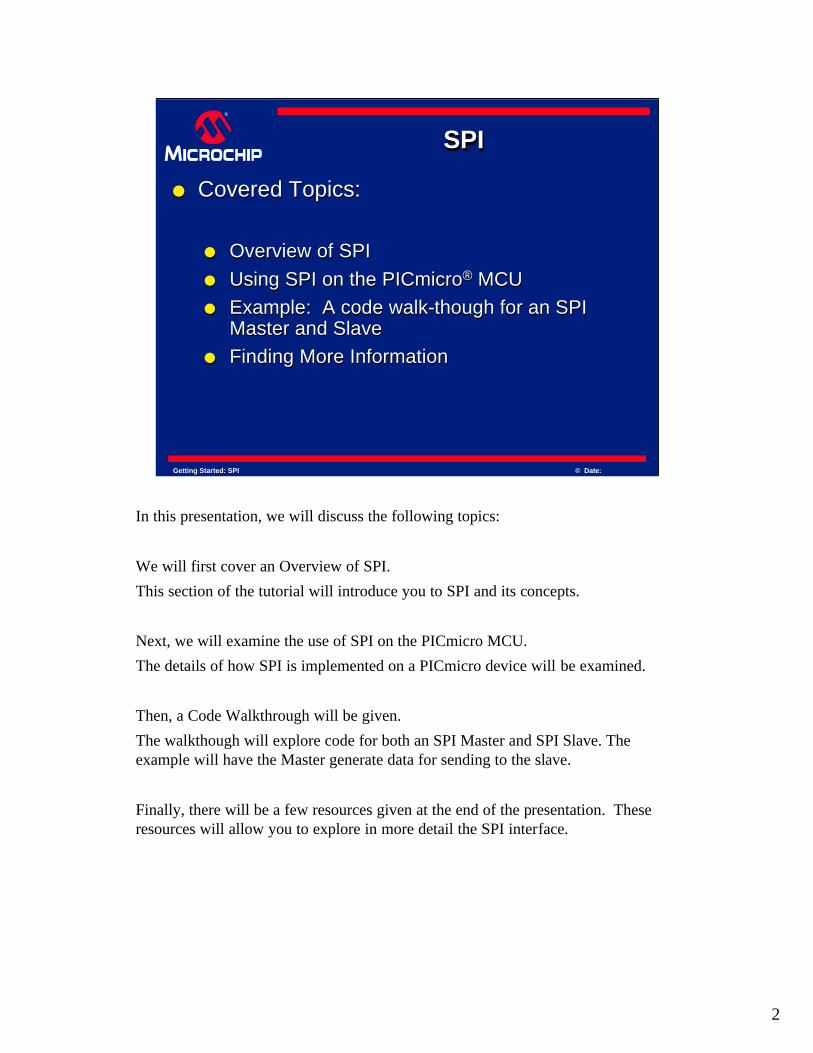
In this presentation, we will discuss the following topics:
We will first cover an Overview of SPI.
This section of the tutorial will introduce you to SPI and its concepts.
Next, we will examine the use of SPI on the PICmicro MCU.
The details of how SPI is implemented on a PICmicro device will be examined.
Then, a Code Walkthrough will be given.
The walkthough will explore code for both an SPI Master and SPI Slave. The example will have the Master generate data for sending to the slave.
Finally, there will be a few resources given at the end of the presentation. These resources will allow you to explore in more detail the SPI interface.
3
Getting Started: SPI © Date:
SPI - OverviewSPI SPI -- OverviewOverview
l SPI stands for Serial Peripheral Interfacel Used for moving data simply and quickly
from one device to anotherl Serial Interfacel Synchronousl Master-Slavel Data Exchange
l SPI stands for Serial Peripheral Interfacel Used for moving data simply and quickly
from one device to anotherl Serial Interfacel Synchronousl Master-Slavel Data Exchange
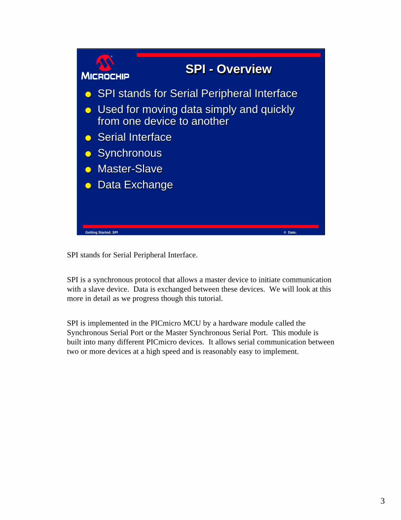
SPI stands for Serial Peripheral Interface.
SPI is a synchronous protocol that allows a master device to initiate communication with a slave device. Data is exchanged between these devices. We will look at this more in detail as we progress though this tutorial.
SPI is implemented in the PICmicro MCU by a hardware module called the Synchronous Serial Port or the Master Synchronous Serial Port. This module is built into many different PICmicro devices. It allows serial communication between two or more devices at a high speed and is reasonably easy to implement.
4
Getting Started: SPI © Date:
SPI - OverviewSPI SPI -- OverviewOverview
l SPI is a Synchronous protocol
l The data is clocked along with a clock signal (SCK)
l The clock signal controls when data is changed and when it should be read
l Since SPI is synchronous, the clock rate can vary, unlike RS-232 style communications
l SPI is a Synchronous protocol
l The data is clocked along with a clock signal (SCK)
l The clock signal controls when data is changed and when it should be read
l Since SPI is synchronous, the clock rate can vary, unlike RS-232 style communications
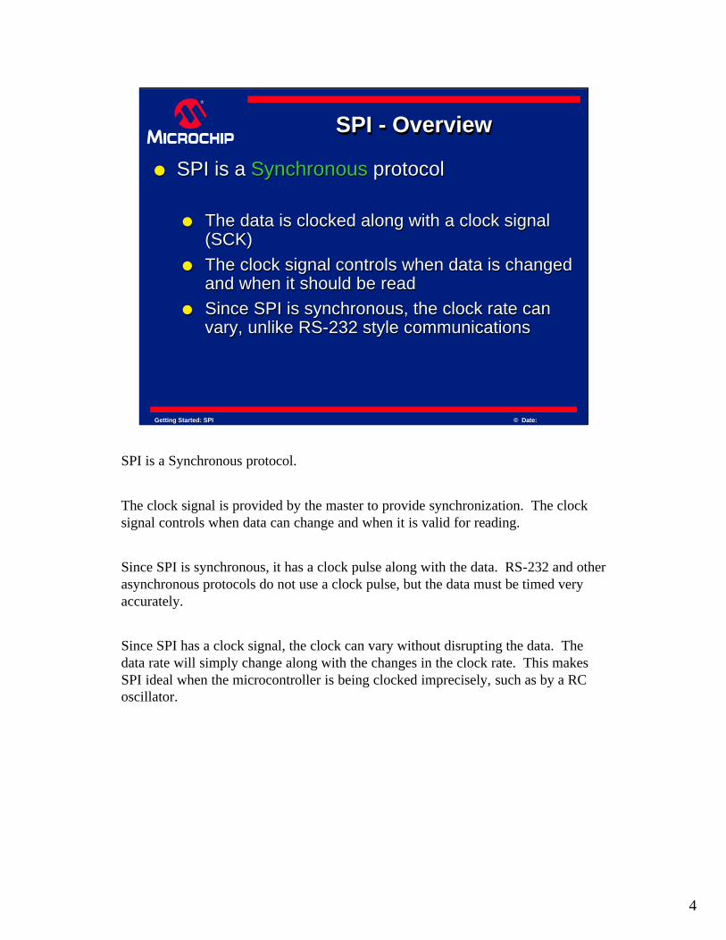
SPI is a Synchronous protocol.
The clock signal is provided by the master to provide synchronization. The clock signal controls when data can change and when it is valid for reading.
Since SPI is synchronous, it has a clock pulse along with the data. RS-232 and other asynchronous protocols do not use a clock pulse, but the data must be timed very accurately.
Since SPI has a clock signal, the clock can vary without disrupting the data. The data rate will simply change along with the changes in the clock rate. This makes SPI ideal when the microcontroller is being clocked imprecisely, such as by a RC oscillator.
5
Getting Started: SPI © Date:
SPI - OverviewSPI SPI -- OverviewOverview
l SPI is a Master-Slave protocol
l The Master device controls the clock (SCK)l No data is transferred unless a clock signal is
presentl All slaves are controlled by the master clockl The slave devices may not manipulate the
clock
l SPI is a Master-Slave protocol
l The Master device controls the clock (SCK)l No data is transferred unless a clock signal is
presentl All slaves are controlled by the master clockl The slave devices may not manipulate the
clock
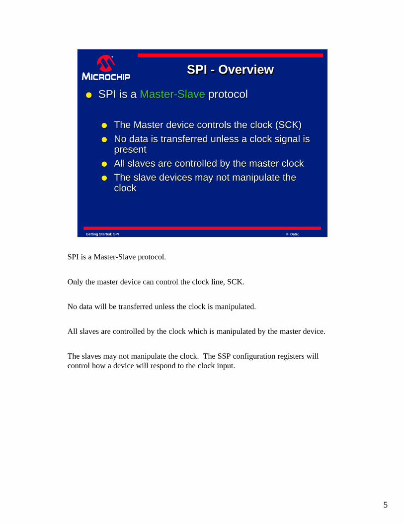
SPI is a Master-Slave protocol.
Only the master device can control the clock line, SCK.
No data will be transferred unless the clock is manipulated.
All slaves are controlled by the clock which is manipulated by the master device.
The slaves may not manipulate the clock. The SSP configuration registers will control how a device will respond to the clock input.
6
Getting Started: SPI © Date:
SPI - OverviewSPI SPI -- OverviewOverview
l SPI is a Data Exchange protocoll As data is being clocked out, new data is
clocked inl Data is exchanged - no device can just be a
transmitter only or receiver onlyl the master controls the exchange by
manipulating the clock line (SCK)
l SPI is a Data Exchange protocoll As data is being clocked out, new data is
clocked inl Data is exchanged - no device can just be a
transmitter only or receiver onlyl the master controls the exchange by
manipulating the clock line (SCK)
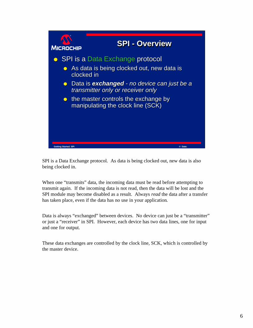
SPI is a Data Exchange protocol. As data is being clocked out, new data is also being clocked in.
When one “transmits” data, the incoming data must be read before attempting to transmit again. If the incoming data is not read, then the data will be lost and the SPI module may become disabled as a result. Always read the data after a transfer has taken place, even if the data has no use in your application.
Data is always “exchanged” between devices. No device can just be a “transmitter” or just a “receiver” in SPI. However, each device has two data lines, one for input and one for output.
These data exchanges are controlled by the clock line, SCK, which is controlled by the master device.

7
Getting Started: SPI © Date:
SPI - OverviewSPI SPI -- OverviewOverview
l SPI is a Data Exchange protocol (continued…)
l Often a signal controls when a device is accessed - this is the CS or SS signal
l CS or SS signal is known as “Chip Select” or “Slave Select” and is frequently an active-low signal.
l SPI is a Data Exchange protocol (continued…)
l Often a signal controls when a device is accessed - this is the CS or SS signal
l CS or SS signal is known as “Chip Select” or “Slave Select” and is frequently an active-low signal.
Often a slave select signal will control when a device is accessed. This signal must be used for when more than one slave exists in a system, but can be optional when only one slave exists in the circuit. As a general rule, it should be used.
This signal is known as the SS signal and stands for “Slave Select.” It indicates to a slave that the master wishes to start an SPI data exchange between that slave device and itself. The signal is most often active low, so a low on this line will indicate the SPI is active, while a high will signal inactivity.
It is often used to improve noise immunity of the system. Its function is to reset the SPI slave so that it is ready to receive the next byte.
8
Getting Started: SPI © Date:
SPI - OverviewSPI SPI -- OverviewOverview
l Data is only output during the rising or falling edge of SCK
l Data is latched during the opposite edge of SCK
l The opposite edge is used to ensure data is valid at the time of reading
l Data is only output during the rising or falling edge of SCK
l Data is latched during the opposite edge of SCK
l The opposite edge is used to ensure data is valid at the time of reading
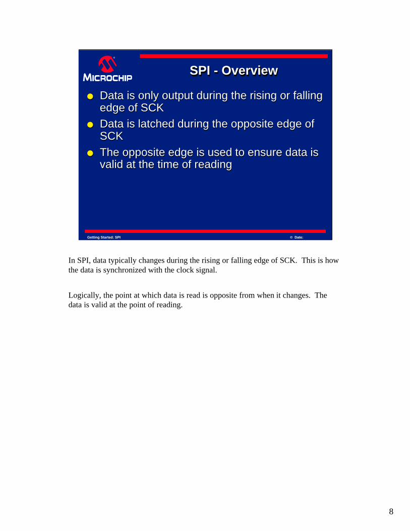
In SPI, data typically changes during the rising or falling edge of SCK. This is how the data is synchronized with the clock signal.
Logically, the point at which data is read is opposite from when it changes. The data is valid at the point of reading.
9
Getting Started: SPI © Date:
SPI - OverviewSPI SPI -- OverviewOverview
SCK
SDO
0 0001 111SDI
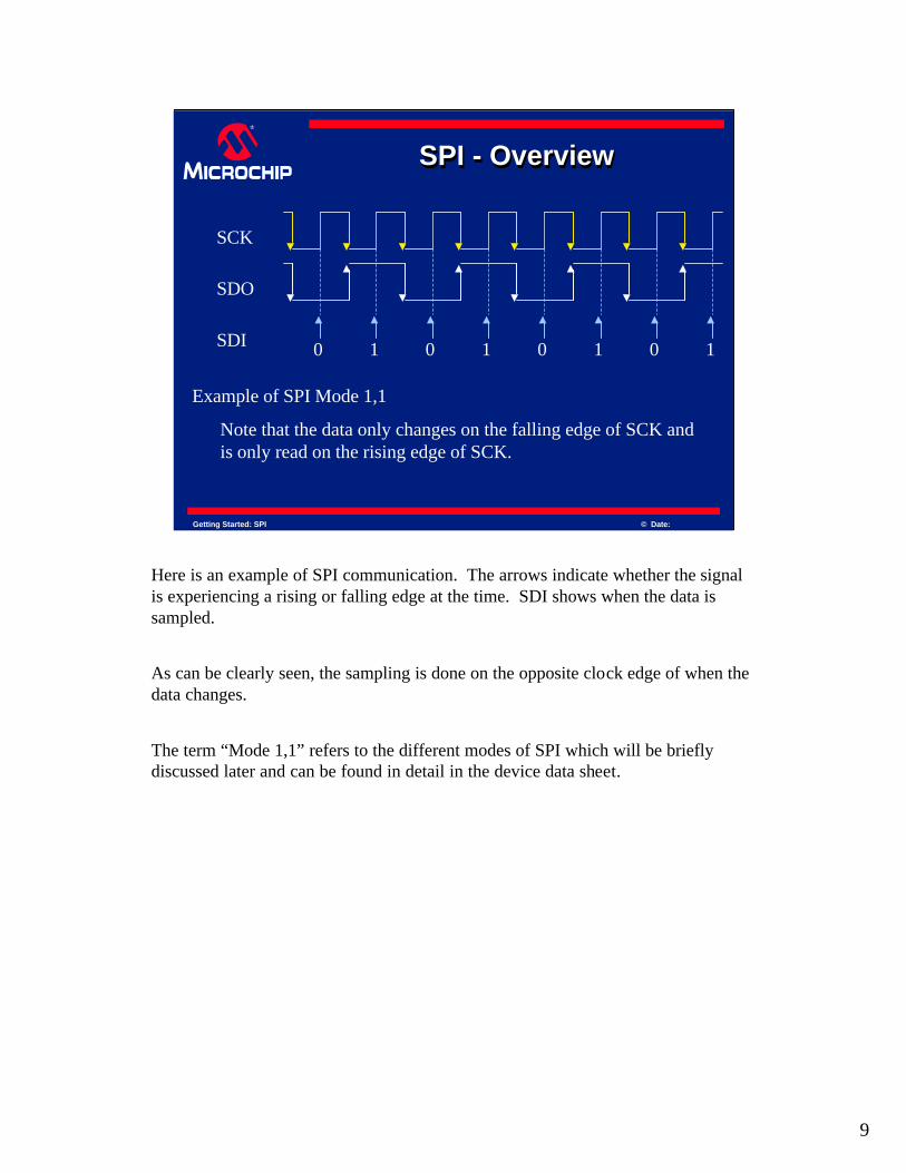
Example of SPI Mode 1,1
Note that the data only changes on the falling edge of SCK and is only read on the rising edge of SCK.
Here is an example of SPI communication. The arrows indicate whether the signal is experiencing a rising or falling edge at the time. SDI shows when the data is sampled.
As can be clearly seen, the sampling is done on the opposite clock edge of when the data changes.
The term “Mode 1,1” refers to the different modes of SPI which will be briefly discussed later and can be found in detail in the device data sheet.
10
Getting Started: SPI © Date:
SPI – PICmicro MCUSPI SPI –– PICmicro MCUPICmicro MCU
l The SSP (or MSSP) module in the PICmicro device allows SPI and other synchronous serial protocols
l The SSP (or MSSP) module in the PICmicro device allows SPI and other synchronous serial protocols
PICmicroMicrocontroller
SSP
PICmicroMicrocontroller
MSSP
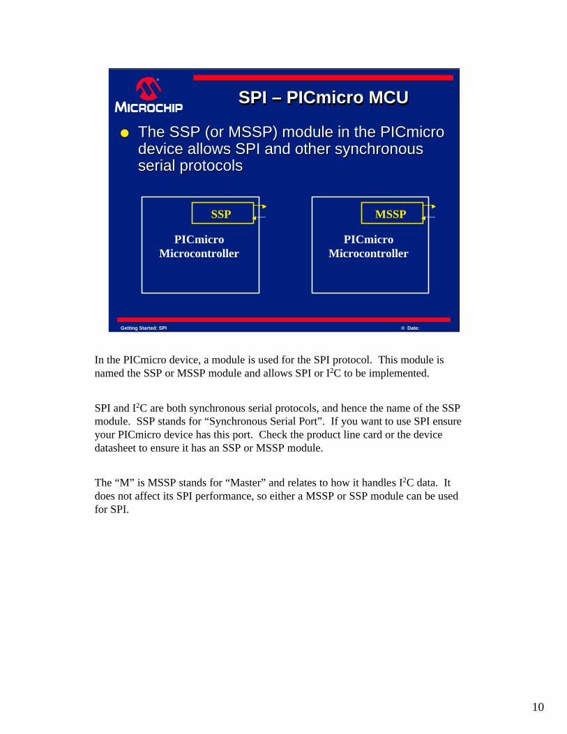
In the PICmicro device, a module is used for the SPI protocol. This module is named the SSP or MSSP module and allows SPI or I2C to be implemented.
SPI and I2C are both synchronous serial protocols, and hence the name of the SSP module. SSP stands for “Synchronous Serial Port”. If you want to use SPI ensure your PICmicro device has this port. Check the product line card or the device datasheet to ensure it has an SSP or MSSP module.
The “M” is MSSP stands for “Master” and relates to how it handles I2C data. It does not affect its SPI performance, so either a MSSP or SSP module can be used for SPI.
11
Getting Started: SPI © Date:
SPI - OverviewSPI SPI -- OverviewOverview
l SPI is a Serial Interface using these signals:
l SS Chip Select or Slave Select When this signal goes low, the slave will listen
for SPI clock and data signals
l SCK Serial ClocK This controls when data is sent and when it is
read
l SPI is a Serial Interface using these signals:
l SS Chip Select or Slave Select When this signal goes low, the slave will listen
for SPI clock and data signals
l SCK Serial ClocK This controls when data is sent and when it is
read
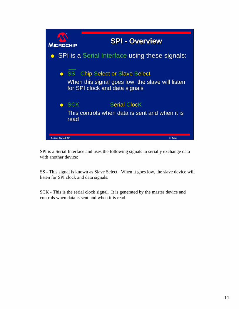
SPI is a Serial Interface and uses the following signals to serially exchange data with another device:
SS - This signal is known as Slave Select. When it goes low, the slave device will listen for SPI clock and data signals.
SCK - This is the serial clock signal. It is generated by the master device and controls when data is sent and when it is read.
12
Getting Started: SPI © Date:
SPI - OverviewSPI SPI -- OverviewOverview
l SDO Serial Data Output This signal carries the data sent out of the
device
l SDI Serial Data Input This signal carries the data sent into the
device
l SDO Serial Data Output This signal carries the data sent out of the
device
l SDI Serial Data Input This signal carries the data sent into the
device
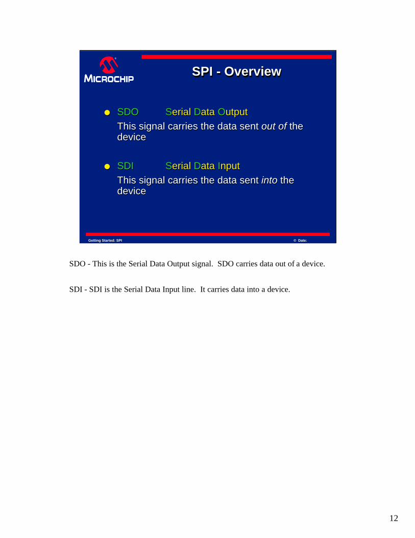
SDO - This is the Serial Data Output signal. SDO carries data out of a device.
SDI - SDI is the Serial Data Input line. It carries data into a device.
13
Getting Started: SPI © Date:
SPI - OverviewSPI SPI -- OverviewOverview
SSPSR SSPSR
SSPBUF SSPBUF
l SPI Data Transfer
Master Slave
SDO
SDOSDI
SDI
Control ControlSCK SCK
SS
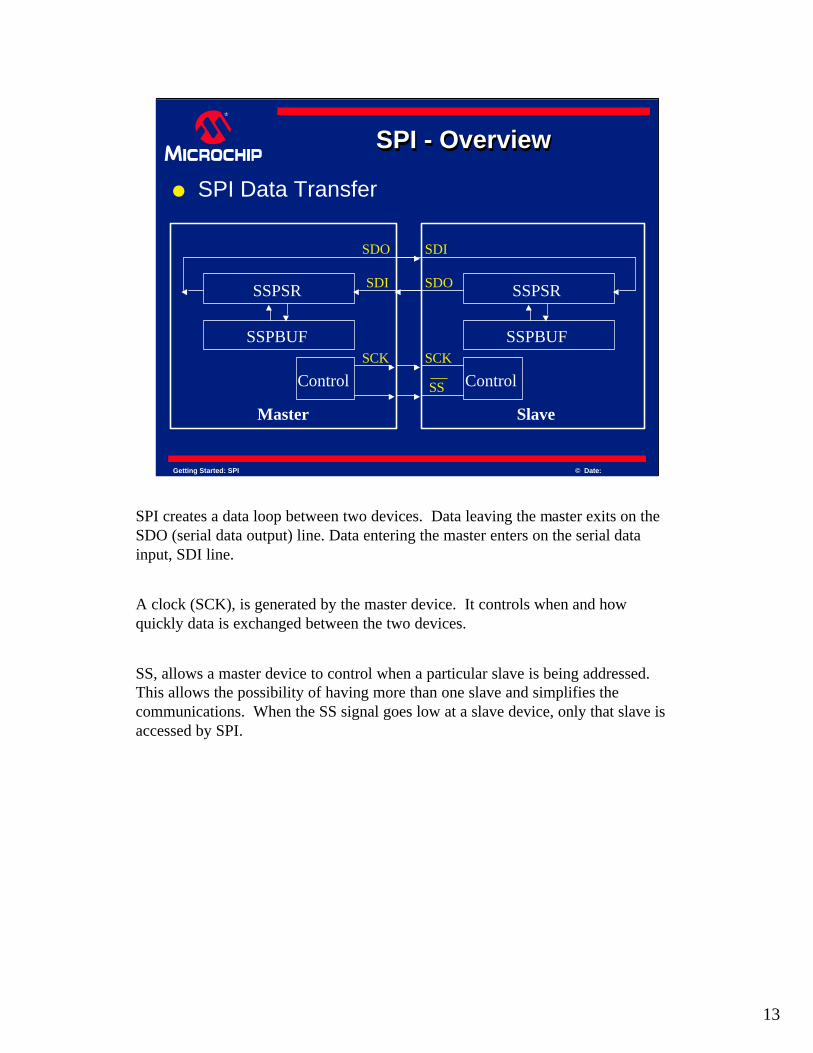
SPI creates a data loop between two devices. Data leaving the master exits on the SDO (serial data output) line. Data entering the master enters on the serial data input, SDI line.
A clock (SCK), is generated by the master device. It controls when and how quickly data is exchanged between the two devices.
SS, allows a master device to control when a particular slave is being addressed. This allows the possibility of having more than one slave and simplifies the communications. When the SS signal goes low at a slave device, only that slave is accessed by SPI.
14
Getting Started: SPI © Date:
SPI - OverviewSPI SPI -- OverviewOverview
SSPSR SSPSR
SSPBUF SSPBUF
l SPI Data Transfer
Master Slave
SDO
SDOSDI
SDI
Control ControlSCK SCK
SS
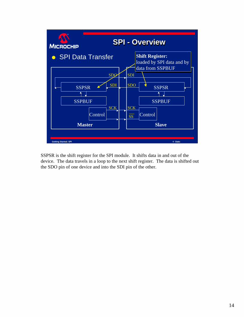
Shift Register:loaded by SPI data and bydata from SSPBUF
SSPSR is the shift register for the SPI module. It shifts data in and out of the device. The data travels in a loop to the next shift register. The data is shifted out the SDO pin of one device and into the SDI pin of the other.
15
Getting Started: SPI © Date:
SPI - OverviewSPI SPI -- OverviewOverview
SSPSR SSPSR
SSPBUF SSPBUF
l SPI Data Transfer
Master Slave
SDO
SDOSDI
SDI
Control ControlSCK SCK
SS
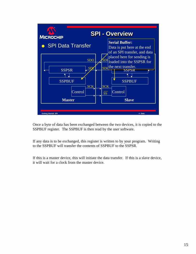
Serial Buffer:Data is put here at the endof an SPI transfer, and dataplaced here for sending isloaded into the SSPSR for the next transfer.
Once a byte of data has been exchanged between the two devices, it is copied to the SSPBUF register. The SSPBUF is then read by the user software.
If any data is to be exchanged, this register is written to by your program. Writing to the SSPBUF will transfer the contents of SSPBUF to the SSPSR.
If this is a master device, this will initiate the data transfer. If this is a slave device, it will wait for a clock from the master device.
16
Getting Started: SPI © Date:
SPI - OverviewSPI SPI -- OverviewOverview
SSPSR SSPSR
SSPBUF SSPBUF
l SPI Data Transfer
Master Slave
SDO
SDOSDI
SDI
Control ControlSCK SCK
SS
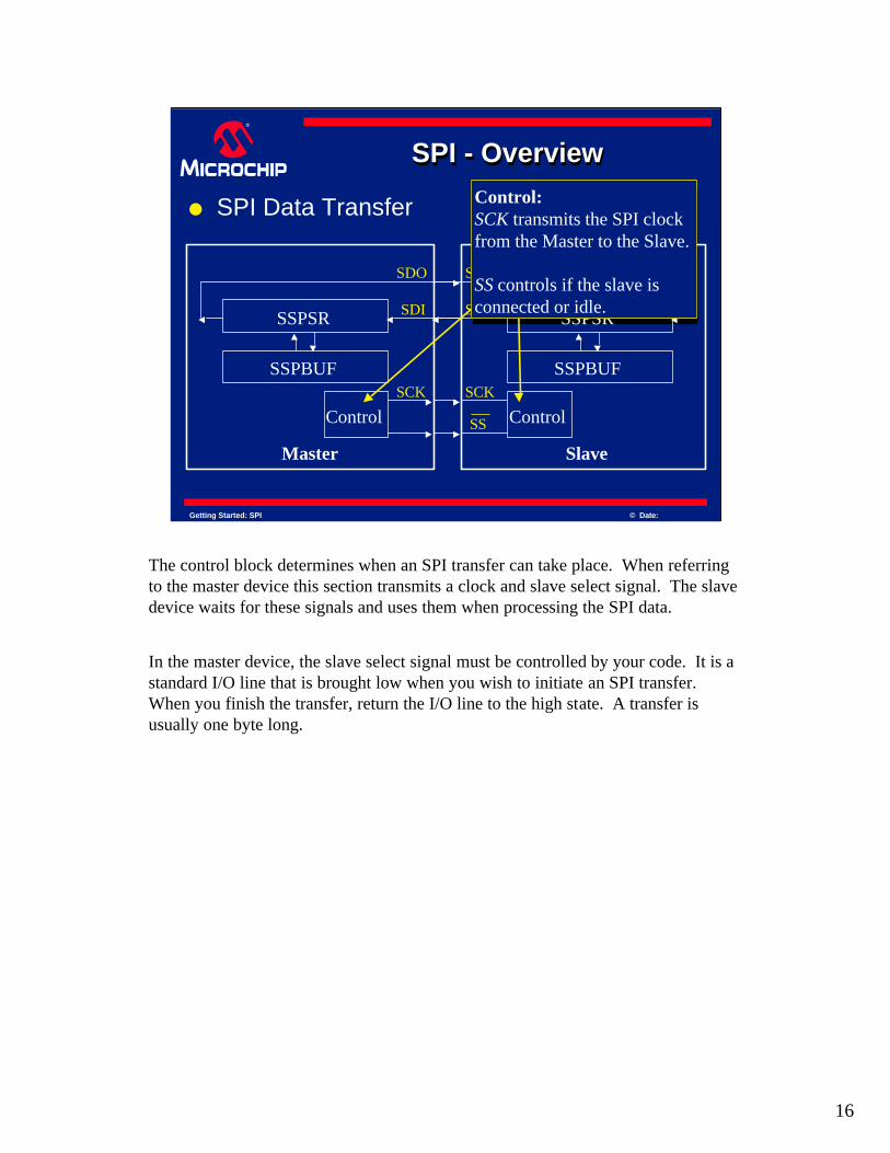
Control:SCK transmits the SPI clock from the Master to the Slave.
SS controls if the slave is connected or idle.
The control block determines when an SPI transfer can take place. When referring to the master device this section transmits a clock and slave select signal. The slave device waits for these signals and uses them when processing the SPI data.
In the master device, the slave select signal must be controlled by your code. It is a standard I/O line that is brought low when you wish to initiate an SPI transfer. When you finish the transfer, return the I/O line to the high state. A transfer is usually one byte long.
17
Getting Started: SPI © Date:
SPI – PICmicro MCUSPI SPI –– PICmicro MCUPICmicro MCU
l 2 Registers control the function of the SPI in the PICmicro MCU
l The values to be placed in the registers will often depend on your application
l See device datasheet for detailsl The next few slides will discuss the registers
that control the SPI module
l 2 Registers control the function of the SPI in the PICmicro MCU
l The values to be placed in the registers will often depend on your application
l See device datasheet for detailsl The next few slides will discuss the registers
that control the SPI module
When using SPI in the PICmicro device, a few registers need to be set up correctly. Two registers run the SPI engine itself, which we will discuss next.
Since there are different modes to SPI and each design can have a number of different devices, the values to set these registers can vary and must be taken into account when designing your system.
The device datasheet will explore these modes more thoroughly.
18
Getting Started: SPI © Date:
SPI – PICmicro MCUSPI SPI –– PICmicro MCUPICmicro MCU
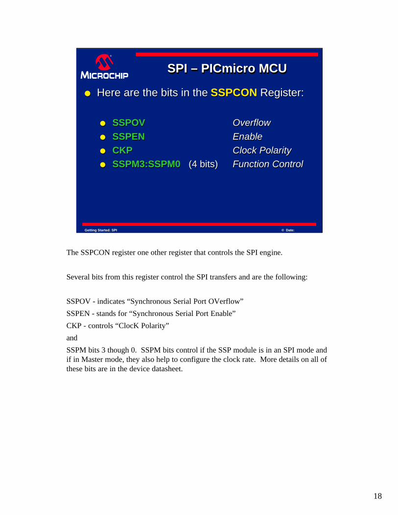
l Here are the bits in the SSPCON Register:
l SSPOV Overflowl SSPEN Enablel CKP Clock Polarityl SSPM3:SSPM0 (4 bits) Function Control
l Here are the bits in the SSPCON Register:
l SSPOV Overflowl SSPEN Enablel CKP Clock Polarityl SSPM3:SSPM0 (4 bits) Function Control
The SSPCON register one other register that controls the SPI engine.
Several bits from this register control the SPI transfers and are the following:
SSPOV - indicates “Synchronous Serial Port OVerflow”
SSPEN - stands for “Synchronous Serial Port Enable”
CKP - controls “ClocK Polarity”
and
SSPM bits 3 though 0. SSPM bits control if the SSP module is in an SPI mode and if in Master mode, they also help to configure the clock rate. More details on all of these bits are in the device datasheet.
19
Getting Started: SPI © Date:
SPI – PICmicro MCUSPI SPI –– PICmicro MCUPICmicro MCU
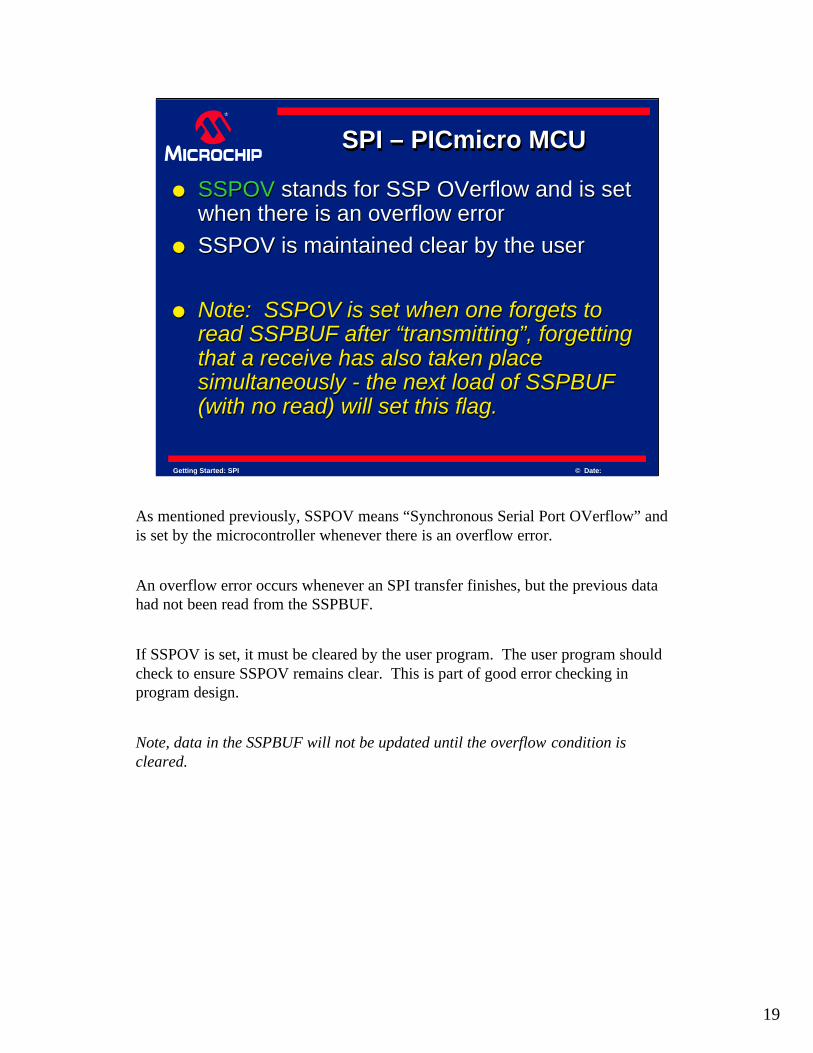
l SSPOV stands for SSP OVerflow and is set when there is an overflow error
l SSPOV is maintained clear by the user
l Note: SSPOV is set when one forgets to read SSPBUF after “transmitting”, forgetting that a receive has also taken place simultaneously - the next load of SSPBUF (with no read) will set this flag.
As mentioned previously, SSPOV means “Synchronous Serial Port OVerflow” and is set by the microcontroller whenever there is an overflow error.
An overflow error occurs whenever an SPI transfer finishes, but the previous data had not been read from the SSPBUF.
If SSPOV is set, it must be cleared by the user program. The user program should check to ensure SSPOV remains clear. This is part of good error checking in program design.
Note, data in the SSPBUF will not be updated until the overflow condition is cleared.
20
Getting Started: SPI © Date:
SPI – PICmicro MCUSPI SPI –– PICmicro MCUPICmicro MCU
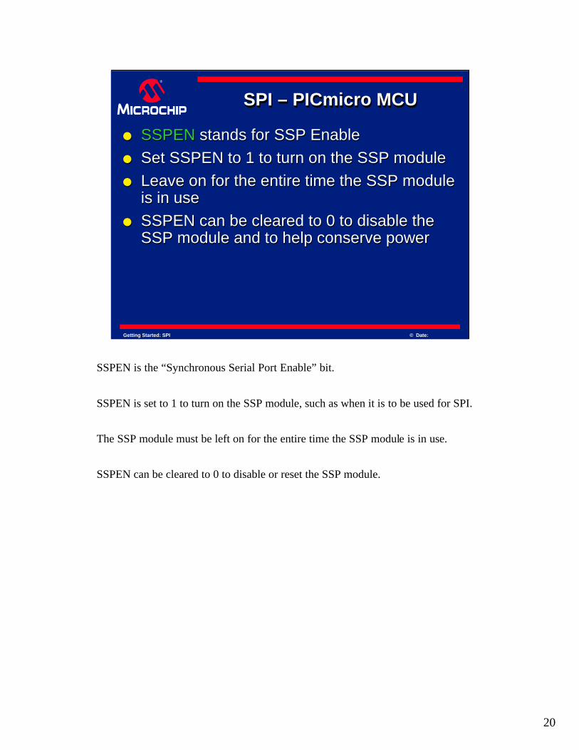
l SSPEN stands for SSP Enable l Set SSPEN to 1 to turn on the SSP modulel Leave on for the entire time the SSP module
is in usel SSPEN can be cleared to 0 to disable the
SSP module and to help conserve power
l SSPEN stands for SSP Enable l Set SSPEN to 1 to turn on the SSP modulel Leave on for the entire time the SSP module
is in usel SSPEN can be cleared to 0 to disable the
SSP module and to help conserve power
SSPEN is the “Synchronous Serial Port Enable” bit.
SSPEN is set to 1 to turn on the SSP module, such as when it is to be used for SPI.
The SSP module must be left on for the entire time the SSP module is in use.
SSPEN can be cleared to 0 to disable or reset the SSP module.
21
Getting Started: SPI © Date:
SPI – PICmicro MCUSPI SPI –– PICmicro MCUPICmicro MCU
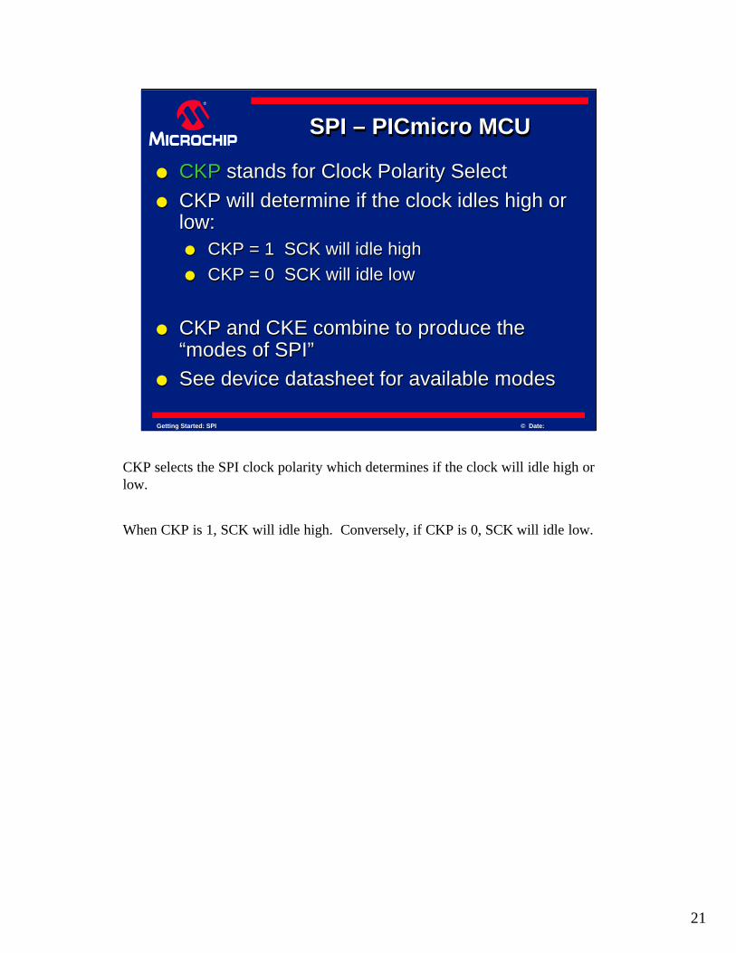
l CKP stands for Clock Polarity Selectl CKP will determine if the clock idles high or
low:l CKP = 1 SCK will idle highl CKP = 0 SCK will idle low
l CKP and CKE combine to produce the “modes of SPI”
l See device datasheet for available modes
l CKP stands for Clock Polarity Selectl CKP will determine if the clock idles high or
low:l CKP = 1 SCK will idle highl CKP = 0 SCK will idle low
l CKP and CKE combine to produce the “modes of SPI”
l See device datasheet for available modes
CKP selects the SPI clock polarity which determines if the clock will idle high or low.
When CKP is 1, SCK will idle high. Conversely, if CKP is 0, SCK will idle low.
22
Getting Started: SPI © Date:
SPI – PICmicro MCUSPI SPI –– PICmicro MCUPICmicro MCU
l Looking at the SSPSTAT Register, three bits help to control SPI transfers:
l SMP Data sample timingl CKE Clock edge selectl BF Buffer full
l Looking at the SSPSTAT Register, three bits help to control SPI transfers:
l SMP Data sample timingl CKE Clock edge selectl BF Buffer full
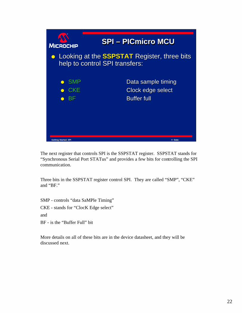
The next register that controls SPI is the SSPSTAT register. SSPSTAT stands for “Synchronous Serial Port STATus” and provides a few bits for controlling the SPI communication.
Three bits in the SSPSTAT register control SPI. They are called “SMP”, “CKE” and “BF.”
SMP - controls “data SaMPle Timing”
CKE - stands for “ClocK Edge select”
and
BF - is the “Buffer Full” bit
More details on all of these bits are in the device datasheet, and they will be discussed next.
23
Getting Started: SPI © Date:
SPI – PICmicro MCUSPI SPI –– PICmicro MCUPICmicro MCU
l SMP controls data SaMPle timingl SMP must be maintained clear for the Slave
PICmicro devicel When in Master Mode:
l 1 = Sample occurs at end of data outputl 0 = Sample occurs in the middle of data output
l This bit controls when received data from SDI line is sampled, relative to when it is sent on the SDO line
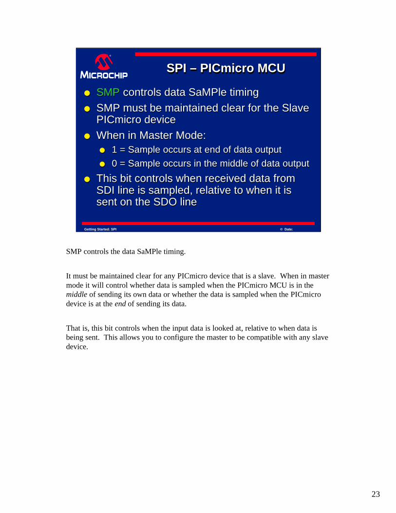
SMP controls the data SaMPle timing.
It must be maintained clear for any PICmicro device that is a slave. When in master mode it will control whether data is sampled when the PICmicro MCU is in the middle of sending its own data or whether the data is sampled when the PICmicro device is at the end of sending its data.
That is, this bit controls when the input data is looked at, relative to when data is being sent. This allows you to configure the master to be compatible with any slave device.
24
Getting Started: SPI © Date:
SPI – PICmicro MCUSPI SPI –– PICmicro MCUPICmicro MCU
l CKE is the Clock Edge Select bitl The function of CKE will depend on the
setting of CKP (see discussion on SSPCON)l This bit controls when data is transmitted
relative to the clock (SCK)l Full details are available in the device data
sheet
l CKE is the Clock Edge Select bitl The function of CKE will depend on the
setting of CKP (see discussion on SSPCON)l This bit controls when data is transmitted
relative to the clock (SCK)l Full details are available in the device data
sheet
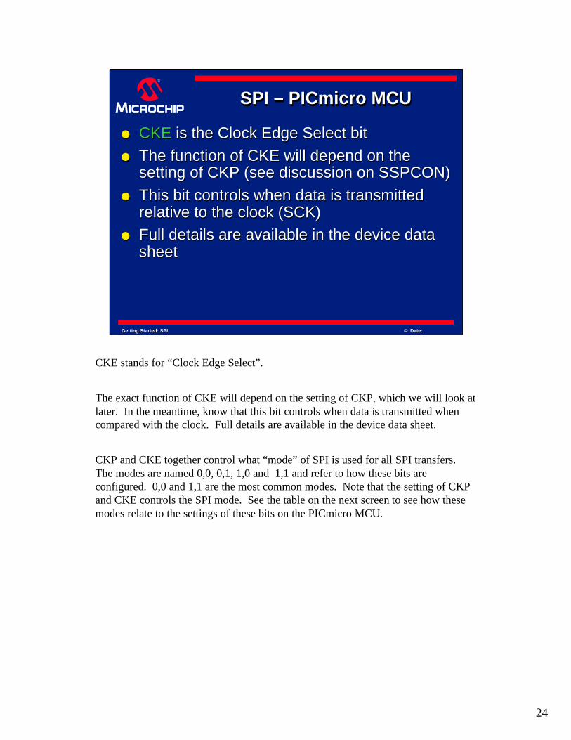
CKE stands for “Clock Edge Select”.
The exact function of CKE will depend on the setting of CKP, which we will look at later. In the meantime, know that this bit controls when data is transmitted when compared with the clock. Full details are available in the device data sheet.
CKP and CKE together control what “mode” of SPI is used for all SPI transfers. The modes are named 0,0, 0,1, 1,0 and 1,1 and refer to how these bits are configured. 0,0 and 1,1 are the most common modes. Note that the setting of CKP and CKE controls the SPI mode. See the table on the next screen to see how these modes relate to the settings of these bits on the PICmicro MCU.
25
Getting Started: SPI © Date:
SPI – PICmicro MCUSPI SPI –– PICmicro MCUPICmicro MCU
SPI Mode and PICmicro MCU SettingsSPI Mode and PICmicro MCU Settings
SPI ModeSPI Mode CKPCKP CKECKE
0,00,0 00 11
0,10,1 00 00
1,01,0 11 11
1,11,1 11 00
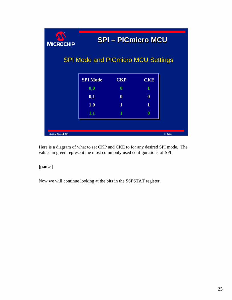
Here is a diagram of what to set CKP and CKE to for any desired SPI mode. The values in green represent the most commonly used configurations of SPI.
[pause]
Now we will continue looking at the bits in the SSPSTAT register.
26
Getting Started: SPI © Date:
SPI – PICmicro MCUSPI SPI –– PICmicro MCUPICmicro MCU
l BF stands for Buffer Full l BF is set when the SSPBUF needs to be
read l BF is set and cleared by the PICmicro MCU
l Note: If the BF flag is set and the SSPBUF register is not read before another byte is exchanged, an overflow will result - see “SSPOV” in previous slides
l BF stands for Buffer Full l BF is set when the SSPBUF needs to be
read l BF is set and cleared by the PICmicro MCU
l Note: If the BF flag is set and the SSPBUF register is not read before another byte is exchanged, an overflow will result - see “SSPOV” in previous slides
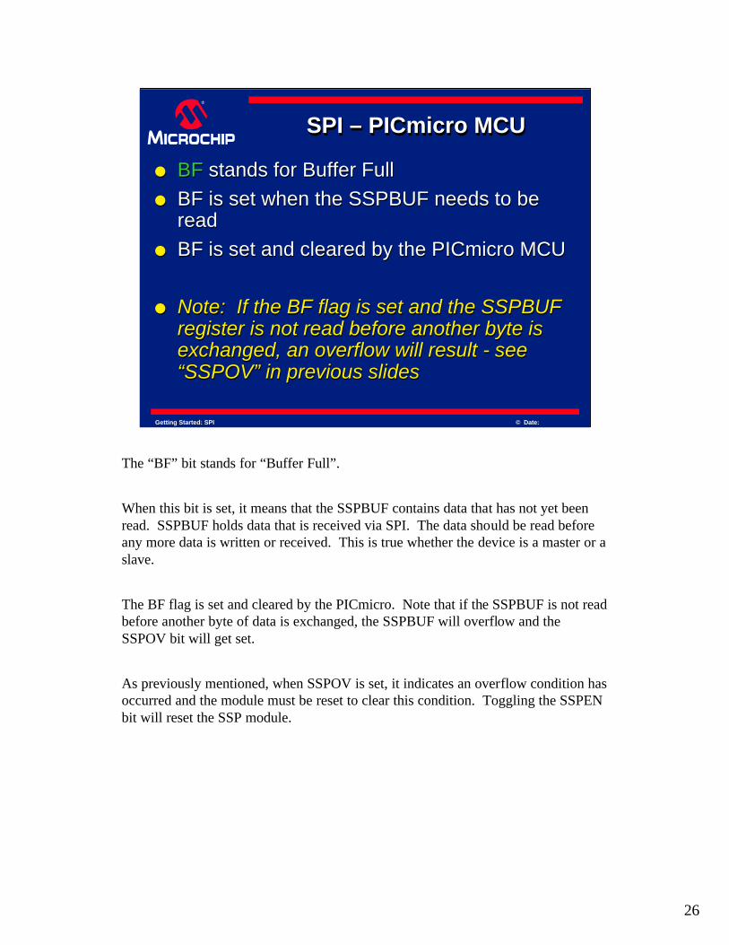
The “BF” bit stands for “Buffer Full”.
When this bit is set, it means that the SSPBUF contains data that has not yet been read. SSPBUF holds data that is received via SPI. The data should be read before any more data is written or received. This is true whether the device is a master or a slave.
The BF flag is set and cleared by the PICmicro. Note that if the SSPBUF is not read before another byte of data is exchanged, the SSPBUF will overflow and the SSPOV bit will get set.
As previously mentioned, when SSPOV is set, it indicates an overflow condition has occurred and the module must be reset to clear this condition. Toggling the SSPEN bit will reset the SSP module.
27
Getting Started: SPI © Date:
SPI - Code ExampleSPI SPI -- Code ExampleCode Example
l Code Example
l Send data from a master to a slave using SPI
l The data comes from a counter, located in the master
l The slave displays the data
l Code Example
l Send data from a master to a slave using SPI
l The data comes from a counter, located in the master
l The slave displays the data
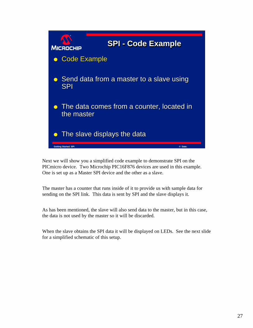
Next we will show you a simplified code example to demonstrate SPI on the PICmicro device. Two Microchip PIC16F876 devices are used in this example. One is set up as a Master SPI device and the other as a slave.
The master has a counter that runs inside of it to provide us with sample data for sending on the SPI link. This data is sent by SPI and the slave displays it.
As has been mentioned, the slave will also send data to the master, but in this case, the data is not used by the master so it will be discarded.
When the slave obtains the SPI data it will be displayed on LEDs. See the next slide for a simplified schematic of this setup.
28
Getting Started: SPI © Date:
SPI - Code ExampleSPI SPI -- Code ExampleCode Example
l Code Examplel Code Example
Master Slave
LEDs
Clock
Data In
Data Out
SPI Link
SDI
SDO
SCKSelectRA2
SDO
SDI
SCK
SS
8POR
T B
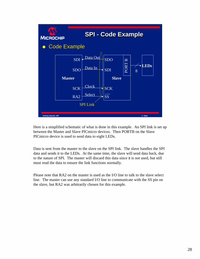
Here is a simplified schematic of what is done in this example. An SPI link is set up between the Master and Slave PICmicro devices. Then PORTB on the Slave PICmicro device is used to send data to eight LEDs.
Data is sent from the master to the slave on the SPI link. The slave handles the SPI data and sends it to the LEDs. At the same time, the slave will send data back, due to the nature of SPI. The master will discard this data since it is not used, but still must read the data to ensure the link functions normally.
Please note that RA2 on the master is used as the I/O line to talk to the slave select line. The master can use any standard I/O line to communicate with the SS pin on the slave, but RA2 was arbitrarily chosen for this example.
29
Getting Started: SPI © Date:
SPI - Master ExampleSPI SPI -- Master ExampleMaster Example
l Code Examplel Code Example
Master Slave
LEDs
Clock
Data In
Data Out
SPI Link
SDI
SDO
SCKSelectRA2
SDO
SDI
SCK
SS
8POR
T B
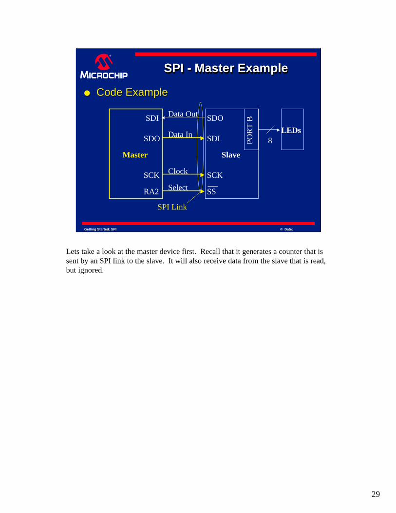
Lets take a look at the master device first. Recall that it generates a counter that is sent by an SPI link to the slave. It will also receive data from the slave that is read, but ignored.
30
Getting Started: SPI © Date:
SPI - Master ExampleSPI SPI -- Master ExampleMaster Example
l Sample SPI Master Code - Flowchartl Sample SPI Master Code - Flowchart
Setup Ports
Setup Variables
Configure SPI
Load SSPBUFwith Data to Send
Did the SPI Transfer Complete?
Read and DiscardData in SSPBUF
Increment Counter and Wait Some Time
Check if SPI Transfer Completed
Start
No
Yes
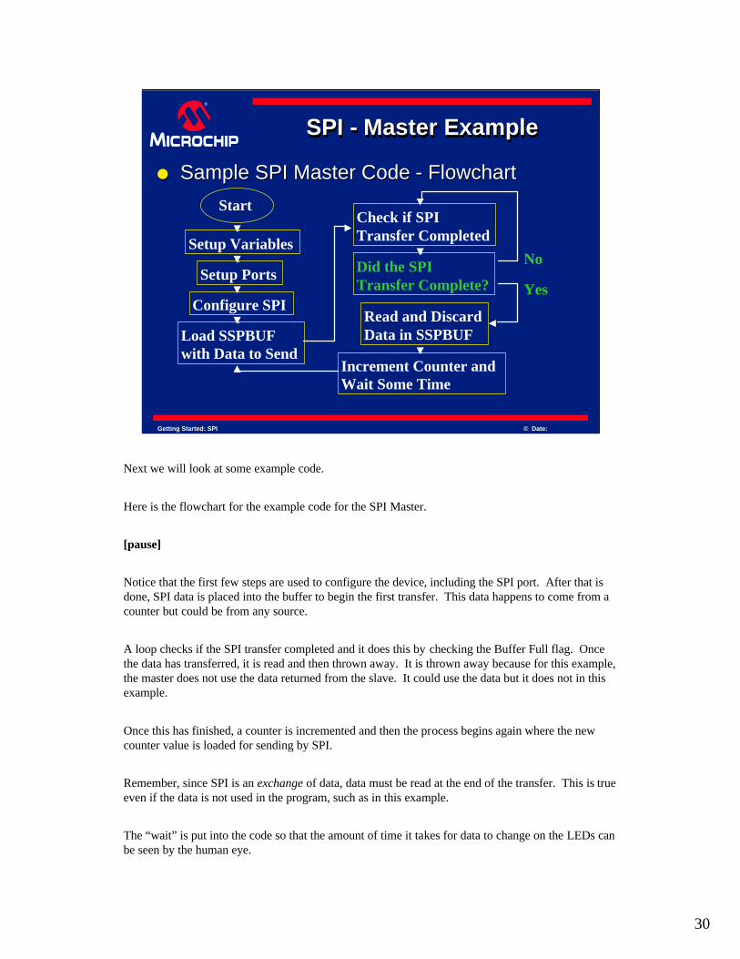
Next we will look at some example code.
Here is the flowchart for the example code for the SPI Master.
[pause]
Notice that the first few steps are used to configure the device, including the SPI port. After that is done, SPI data is placed into the buffer to begin the first transfer. This data happens to come from a counter but could be from any source.
A loop checks if the SPI transfer completed and it does this by checking the Buffer Full flag. Once the data has transferred, it is read and then thrown away. It is thrown away because for this example, the master does not use the data returned from the slave. It could use the data but it does not in this example.
Once this has finished, a counter is incremented and then the process begins again where the new counter value is loaded for sending by SPI.
Remember, since SPI is an exchange of data, data must be read at the end of the transfer. This is true even if the data is not used in the program, such as in this example.
The “wait” is put into the code so that the amount of time it takes for data to change on the LEDs can be seen by the human eye.

31
Getting Started: SPI © Date:
SPI - Master ExampleSPI SPI -- Master ExampleMaster ExampleSend_DT bcf PORTA,CS ; Enable Chip Select Output (low)
movf Ctr0,W ; Get Ctr (Counter Value) in Wmovwf SSPBUF ; put in SSPBUFBANKSEL SSPSTAT ; BANK 1
Char1 btfss SSPSTAT,BF ; Data transfer complete? (Buffer Full?)goto Char1 ; if not, check againBANKSEL SSPBUF ; BANK0movf SSPBUF,W ; Get Data from SSPBUF; ; Throw it away
bsf PORTA,CS ; Disable Chip Select Output (high)
Update_Test_Counterincf Ctr0,F ; Increment counter variable
Delay movlw 0x01 ; Simple Delay loopmovwf Dly1 ; |movlw 0x0F ; |movwf Dly0 ; |
DlyLoop decfsz Dly0,F ; |goto DlyLoop ; |decfsz Dly1,F ; |goto DlyLoop ; |; Done Delay ; \_/
DoAgain goto Send_DT ; Done, Send Next Byte.
end
; SPItstM0.asm; MASTER Rev 0; Demonstrates SPI connection between 2 PICmicro devices; Master sends data (a counter), Slave receives and outputs to LEDs on PORTB
list p=16F876#include "p16F876.inc"
Ctr0 EQU 0x20 ; Counter variable - sent to SPI Dly0 EQU 0x21 ; Delay Variable (low byte)Dly1 EQU 0x22 ; Delay Variable (high byte)
#define CS 0x02 ; PORTA,2
ORG 0 ; Begin Code at location 0nop ; FOR ICD
; Set up the SPI SupportBANKSEL TRISA ; BANK 1movlw 0x00 ; Set PORTA asmovwf TRISA ; all Outputsmovlw 0x06 ; Turn off A/Dmovwf ADCON1 ; so PORTA can be used
; Set up the SPI PortBANKSEL TRISC ; BANK 1movlw 0x10 ; SCK is output (Master), SDI is input, movwf TRISC ; SDO is output, all others outputmovlw 0x40 ; Mode 1,1 SPI, middle of output movwf SSPSTAT ; time samplingBANKSEL SSPCON ; BANK 0movlw 0x31 ; Mode 1,1 SPI Master Mode, 1/16 Tosc bit
timemovwf SSPCON ; SSP is on
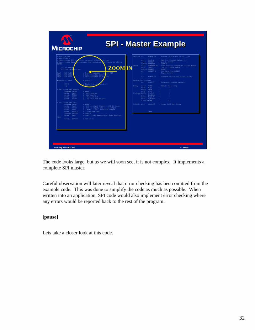
Here is the complete code. This example will show a complete code example and not just a small sample. The actual SPI code is just a small part of this.
32
Getting Started: SPI © Date:
SPI - Master ExampleSPI SPI -- Master ExampleMaster ExampleSend_DT bcf PORTA,CS ; Enable Chip Select Output (low)
movf Ctr0,W ; Get Ctr (Counter Value) in Wmovwf SSPBUF ; put in SSPBUFBANKSEL SSPSTAT ; BANK 1
Char1 btfss SSPSTAT,BF ; Data transfer complete? (Buffer Full?)goto Char1 ; if not, check againBANKSEL SSPBUF ; BANK0movf SSPBUF,W ; Get Data from SSPBUF; ; Throw it away
bsf PORTA,CS ; Disable Chip Select Output (high)
Update_Test_Counterincf Ctr0,F ; Increment counter variable
Delay movlw 0x01 ; Simple Delay loopmovwf Dly1 ; |movlw 0x0F ; |movwf Dly0 ; |
DlyLoop decfsz Dly0,F ; |goto DlyLoop ; |decfsz Dly1,F ; |goto DlyLoop ; |; Done Delay ; \_/
DoAgain goto Send_DT ; Done, Send Next Byte.
end
; SPItstM0.asm; MASTER Rev 0; Demonstrates SPI connection between 2 PICmicro devices; Master sends data (a counter), Slave receives and outputs to LEDs on PORTB
list p=16F876#include "p16F876.inc"
Ctr0 EQU 0x20 ; Counter variable - sent to SPI Dly0 EQU 0x21 ; Delay Variable (low byte)Dly1 EQU 0x22 ; Delay Variable (high byte)
#define CS 0x02 ; PORTA,2
ORG 0 ; Begin Code at location 0nop ; FOR ICD
; Set up the SPI SupportBANKSEL TRISA ; BANK 1movlw 0x00 ; Set PORTA asmovwf TRISA ; all Outputsmovlw 0x06 ; Turn off A/Dmovwf ADCON1 ; so PORTA can be used
; Set up the SPI PortBANKSEL TRISC ; BANK 1movlw 0x10 ; SCK is output (Master), SDI is input, movwf TRISC ; SDO is output, all others outputmovlw 0x40 ; Mode 1,1 SPI, middle of output movwf SSPSTAT ; time samplingBANKSEL SSPCON ; BANK 0movlw 0x31 ; Mode 1,1 SPI Master Mode, 1/16 Tosc bit
timemovwf SSPCON ; SSP is on
ZOOM IN
The code looks large, but as we will soon see, it is not complex. It implements a complete SPI master.
Careful observation will later reveal that error checking has been omitted from the example code. This was done to simplify the code as much as possible. When written into an application, SPI code would also implement error checking where any errors would be reported back to the rest of the program.
[pause]
Lets take a closer look at this code.
33
Getting Started: SPI © Date:
SPI - Master ExampleSPI SPI -- Master ExampleMaster Example
; SPItstM0.asm; MASTER Rev 0; Demonstrates SPI connection between 2 PICmicro devices; Master sends data (a counter), Slave receives and outputs to LEDs on PORTB
list p=16F876#include "p16F876.inc"
__CONFIG _CP_OFF & _DEBUG_OFF & _WRT_ENABLE_OFF & _CPD_OFF & _LVP_OFF & _BODEN_OFF & _PWRTE_ON & _WDT_OFF_ & _XT_OSC
Ctr0 EQU 0x20 ; Counter variable - sent to SPI Dly0 EQU 0x21 ; Delay Variable (low byte)Dly1 EQU 0x22 ; Delay Variable (high byte)
#define SS PORTA,2 ; Slave Select (RA2)
Comments
Variables
Processor setup
Define
Configuration Bits
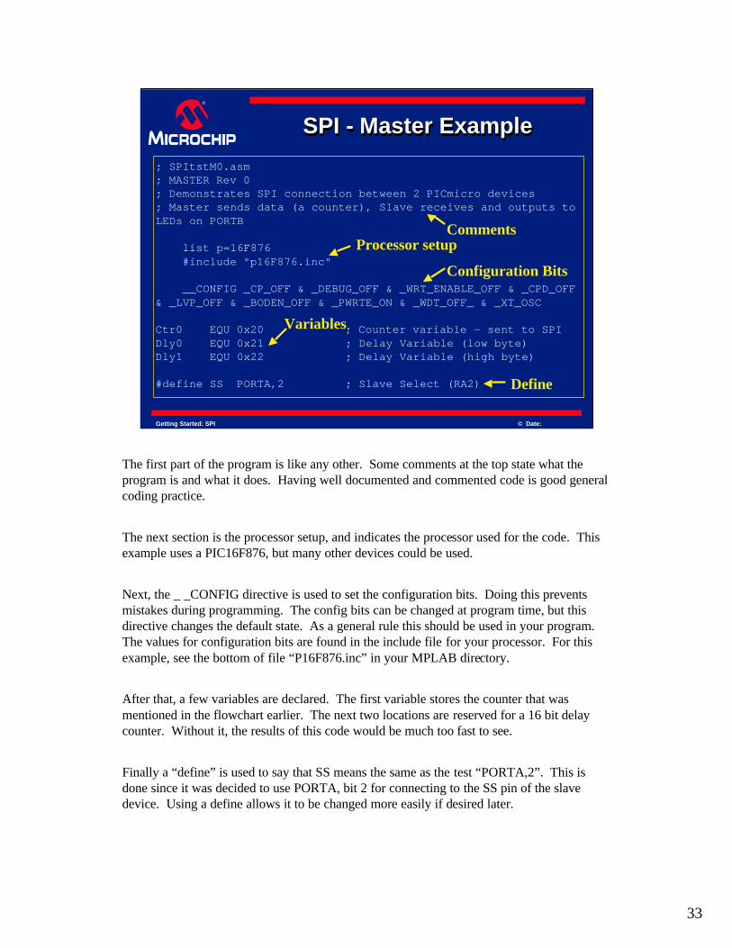
The first part of the program is like any other. Some comments at the top state what the program is and what it does. Having well documented and commented code is good general coding practice.
The next section is the processor setup, and indicates the processor used for the code. This example uses a PIC16F876, but many other devices could be used.
Next, the _ _CONFIG directive is used to set the configuration bits. Doing this prevents mistakes during programming. The config bits can be changed at program time, but this directive changes the default state. As a general rule this should be used in your program. The values for configuration bits are found in the include file for your processor. For this example, see the bottom of file “P16F876.inc” in your MPLAB directory.
After that, a few variables are declared. The first variable stores the counter that was mentioned in the flowchart earlier. The next two locations are reserved for a 16 bit delay counter. Without it, the results of this code would be much too fast to see.
Finally a “define” is used to say that SS means the same as the test “PORTA,2”. This is done since it was decided to use PORTA, bit 2 for connecting to the SS pin of the slave device. Using a define allows it to be changed more easily if desired later.
34
Getting Started: SPI © Date:
SPI - Master ExampleSPI SPI -- Master ExampleMaster Example
ORG 0 ; Begin Code at location 0nop ; FOR ICD
; Set up the SPI SupportBANKSEL TRISA ; BANK 1movlw 0x00 ; Set PORTA asmovwf TRISA ; all Outputsmovlw 0x06 ; Turn off A/Dmovwf ADCON1 ; so PORTA can be used
Code start
Port setup
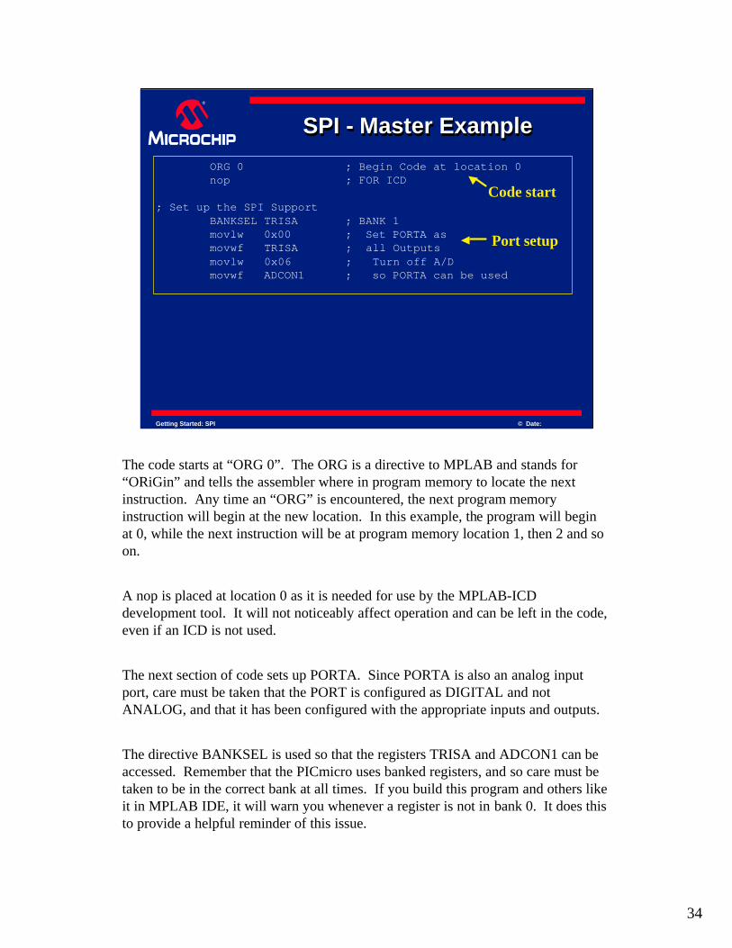
The code starts at “ORG 0”. The ORG is a directive to MPLAB and stands for “ORiGin” and tells the assembler where in program memory to locate the next instruction. Any time an “ORG” is encountered, the next program memory instruction will begin at the new location. In this example, the program will begin at 0, while the next instruction will be at program memory location 1, then 2 and so on.
A nop is placed at location 0 as it is needed for use by the MPLAB-ICD development tool. It will not noticeably affect operation and can be left in the code, even if an ICD is not used.
The next section of code sets up PORTA. Since PORTA is also an analog input port, care must be taken that the PORT is configured as DIGITAL and not ANALOG, and that it has been configured with the appropriate inputs and outputs.
The directive BANKSEL is used so that the registers TRISA and ADCON1 can be accessed. Remember that the PICmicro uses banked registers, and so care must be taken to be in the correct bank at all times. If you build this program and others like it in MPLAB IDE, it will warn you whenever a register is not in bank 0. It does this to provide a helpful reminder of this issue.
35
Getting Started: SPI © Date:
SPI - Master ExampleSPI SPI -- Master ExampleMaster Example
; Set up the SPI PortBANKSEL TRISC ; BANK 1movlw B’00010000’ ; SCK is output (Master), SDI is
; input, movwf TRISC ; SDO is output, all others
; output
movlw B’01000000’ ; SPI, middle ofmovwf SSPSTAT ; output time samplingBANKSEL SSPCON ; BANK 0movlw B’0011001’ ; Mode 1,1 SPI Master Mode, 1/16
; Tosc bit timemovwf SSPCON ; SSP is on
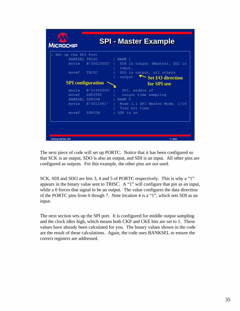
Set I/O direction for SPI useSPI configuration
The next piece of code will set up PORTC. Notice that it has been configured so that SCK is an output, SDO is also an output, and SDI is an input. All other pins are configured as outputs. For this example, the other pins are not used.
SCK, SDI and SDO are bits 3, 4 and 5 of PORTC respectively. This is why a “1” appears in the binary value sent to TRISC. A “1” will configure that pin as an input, while a 0 forces that signal to be an output. The value configures the data direction of the PORTC pins from 0 though 7. Note location 4 is a “1”, which sets SDI as an input.
The next section sets up the SPI port. It is configured for middle output sampling and the clock idles high, which means both CKP and CKE bits are set to 1. These values have already been calculated for you. The binary values shown in the code are the result of these calculations. Again, the code uses BANKSEL to ensure the correct registers are addressed.
36
Getting Started: SPI © Date:
SPI - Master ExampleSPI SPI -- Master ExampleMaster Example
Send_DT bcf SS ; Enable Chip Select Output (low)
movf Ctr0,W ; Get Ctr (Counter Value) in Wmovwf SSPBUF ; put in SSPBUFBANKSEL SSPSTAT ; BANK 1
Char1 btfss SSPSTAT,BF ; Data transfer complete? ; (Buffer Full?)
goto Char1 ; if not, check again
BANKSEL SSPBUF ; BANK0movf SSPBUF,W ; Read SSPBUF register
; data is not used
bsf SS ; Disable Slave Select Output; (high)
Send SPI Data to Buffer
Check Flag
Get Received Data
Done with Transfer
Start Transfer
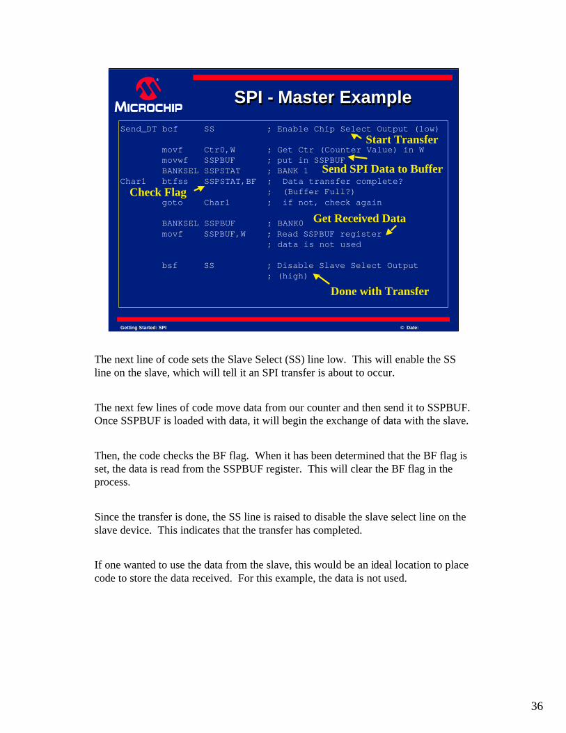
The next line of code sets the Slave Select (SS) line low. This will enable the SS line on the slave, which will tell it an SPI transfer is about to occur.
The next few lines of code move data from our counter and then send it to SSPBUF. Once SSPBUF is loaded with data, it will begin the exchange of data with the slave.
Then, the code checks the BF flag. When it has been determined that the BF flag is set, the data is read from the SSPBUF register. This will clear the BF flag in the process.
Since the transfer is done, the SS line is raised to disable the slave select line on the slave device. This indicates that the transfer has completed.
If one wanted to use the data from the slave, this would be an ideal location to place code to store the data received. For this example, the data is not used.
37
Getting Started: SPI © Date:
SPI - Master ExampleSPI SPI -- Master ExampleMaster Example
Update_Test_Counterincf Ctr0,F ; Increment counter variable
Delay movlw H’F0’ ; Simple Delay loopmovwf Dly1 ; |movlw H’0F’ ; |movwf Dly0 ; |
DlyLoop decfsz Dly0,F ; |goto DlyLoop ; |decfsz Dly1,F ; |goto DlyLoop ; |; Done Delay ; \_/
DoAgain goto Send_DT ; Done, Send Next Byte.
END
Delay LoopMakes Increment Rate Visible
Go To Transfer More SPI Data
End of program
Increment Counter
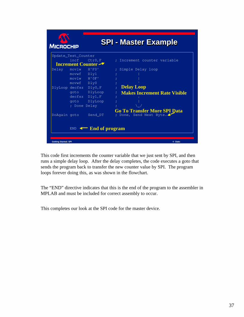
This code first increments the counter variable that we just sent by SPI, and then runs a simple delay loop. After the delay completes, the code executes a goto that sends the program back to transfer the new counter value by SPI. The program loops forever doing this, as was shown in the flowchart.
The “END” directive indicates that this is the end of the program to the assembler in MPLAB and must be included for correct assembly to occur.
This completes our look at the SPI code for the master device.
38
Getting Started: SPI © Date:
SPI - Slave ExampleSPI SPI -- Slave ExampleSlave Example
l Code Examplel Code Example
Master Slave
LEDs
Clock
Data In
Data Out
SPI Link
SDI
SDO
SCKSelectRA2
SDO
SDI
SCK
SS
8POR
T B
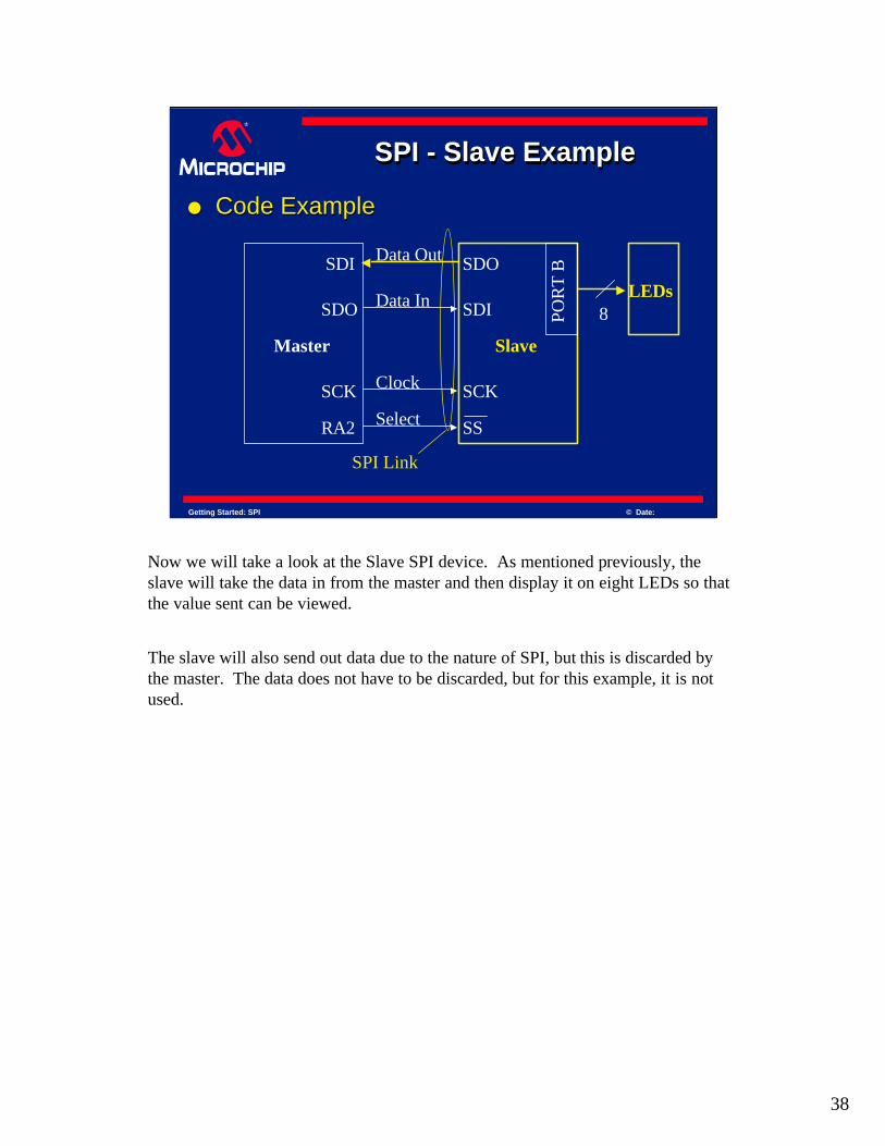
Now we will take a look at the Slave SPI device. As mentioned previously, the slave will take the data in from the master and then display it on eight LEDs so that the value sent can be viewed.
The slave will also send out data due to the nature of SPI, but this is discarded by the master. The data does not have to be discarded, but for this example, it is not used.
39
Getting Started: SPI © Date:
SPI - Slave ExampleSPI SPI -- Slave ExampleSlave Example
l Sample SPI Slave Code - Flowchartl Sample SPI Slave Code - Flowchart
Setup Ports
Setup Variables
Configure SPIDid the SPI Transfer Complete?
Read the SPI Data
Display Result
Check if SPI Transfer Completed
Start
No
Yes
* NOTE: There is no data to send so SSPBUF is not loaded with new data in this example.
Load SSPBUF *with Data to Send
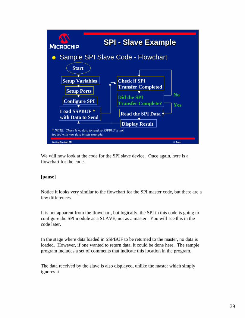
We will now look at the code for the SPI slave device. Once again, here is a flowchart for the code.
[pause]
Notice it looks very similar to the flowchart for the SPI master code, but there are a few differences.
It is not apparent from the flowchart, but logically, the SPI in this code is going to configure the SPI module as a SLAVE, not as a master. You will see this in the code later.
In the stage where data loaded in SSPBUF to be returned to the master, no data is loaded. However, if one wanted to return data, it could be done here. The sample program includes a set of comments that indicate this location in the program.
The data received by the slave is also displayed, unlike the master which simply ignores it.
40
Getting Started: SPI © Date:
SPI - Slave ExampleSPI SPI -- Slave ExampleSlave ExampleChk4Dat movlw SSPSTAT ; Indirectly test
movwf FSR ; a register by loading FSRbtfss INDF,BF ; Here is the testgoto Skip_ND ; New data, do a transfer (below
RX_Data BANKSEL SSPBUF ; BANK 0movf SSPBUF,W ; put in SSPBUF into WBANKSEL PORTB ; BANK 0movwf PORTB ; Show the results on PORTB
DoAgain; Optional customer code can go heregoto Chk4Dat ; Receive Next Byte
end
; SPItstS0.asm; SLAVE Rev 0; Demonstrates SPI connection between 2 PICs; Master sends data (a counter), Slave receives and outputs to LEDs ; on PORTB
list p=16F876#include "p16F876.inc"
#define CS 0x20 ; PORTA,5 (HW SS pin)
ORG 0
nop ; FOR ICD
; Set up the SPI SupportBANKSEL TRISA ; BANK 1movlw CS ; Chip Select pinmovwf TRISA ; is in input modemovlw 0x06 ; Turn Off A/D mode for at least the movwf ADCON1 ; Chip Select pin (all Digital mode)
; Set up output portBANKSEL TRISB ; BANK 1movlw 0x00 ; Configure all PORTB pins movwf TRISB ; to be in output mode
; Set up the SPIBANKSEL TRISC ; BANK 1movlw 0x18 ; SCK is input (Slave), SDI is input, movwf TRISC ; SDO is output, all others output
movlw 0x40 ; Mode 1,1 SPI withmovwf SSPSTAT ; middle of output time sampling
BANKSEL SSPCON ; BANK 0movlw 0x34 ; Mode 1,1 SPI Slave Mode, /SS Requiredmovwf SSPCON ; SSP is on
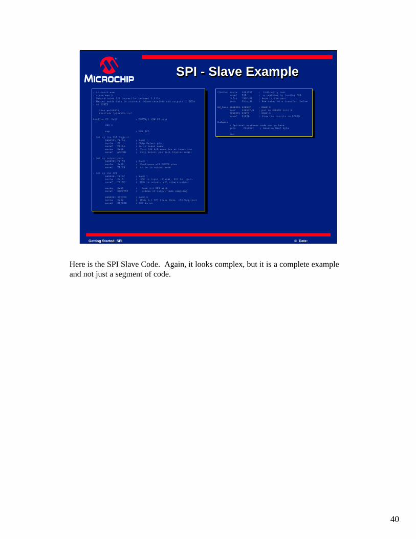
Here is the SPI Slave Code. Again, it looks complex, but it is a complete example and not just a segment of code.
41
Getting Started: SPI © Date:
SPI - Slave ExampleSPI SPI -- Slave ExampleSlave ExampleChk4Dat movlw SSPSTAT ; Indirectly test
movwf FSR ; a register by loading FSRbtfss INDF,BF ; Here is the testgoto Skip_ND ; New data, do a transfer (below
RX_Data BANKSEL SSPBUF ; BANK 0movf SSPBUF,W ; put in SSPBUF into WBANKSEL PORTB ; BANK 0movwf PORTB ; Show the results on PORTB
DoAgain; Optional customer code can go heregoto Chk4Dat ; Receive Next Byte
end
; SPItstS0.asm; SLAVE Rev 0; Demonstrates SPI connection between 2 PICs; Master sends data (a counter), Slave receives and outputs to LEDs ; on PORTB
list p=16F876#include "p16F876.inc"
#define CS 0x20 ; PORTA,5 (HW SS pin)
ORG 0
nop ; FOR ICD
; Set up the SPI SupportBANKSEL TRISA ; BANK 1movlw CS ; Chip Select pinmovwf TRISA ; is in input modemovlw 0x06 ; Turn Off A/D mode for at least the movwf ADCON1 ; Chip Select pin (all Digital mode)
; Set up output portBANKSEL TRISB ; BANK 1movlw 0x00 ; Configure all PORTB pins movwf TRISB ; to be in output mode
; Set up the SPIBANKSEL TRISC ; BANK 1movlw 0x18 ; SCK is input (Slave), SDI is input, movwf TRISC ; SDO is output, all others output
movlw 0x40 ; Mode 1,1 SPI withmovwf SSPSTAT ; middle of output time sampling
BANKSEL SSPCON ; BANK 0movlw 0x34 ; Mode 1,1 SPI Slave Mode, /SS Requiredmovwf SSPCON ; SSP is on
ZOOM IN
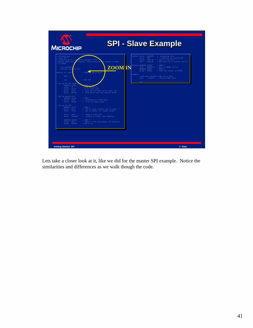
Lets take a closer look at it, like we did for the master SPI example. Notice the similarities and differences as we walk though the code.
42
Getting Started: SPI © Date:
SPI - Slave ExampleSPI SPI -- Slave ExampleSlave Example
; SPItstS0.asm; SLAVE Rev 0; Demonstrates SPI connection between 2 PICs; Master sends data (a counter), Slave receives and outputs to ; LEDs on PORTB
list p=16F876#include "p16F876.inc"
__CONFIG _CP_OFF & _DEBUG_OFF & _WRT_ENABLE_OFF & _CPD_OFF & _LVP_OFF & _BODEN_OFF & _PWRTE_ON & _WDT_OFF & _XT_OSC
ORG 0 ; Begin program at location 0
Processor Setup
Start of Program
Comments
Configuration Bits
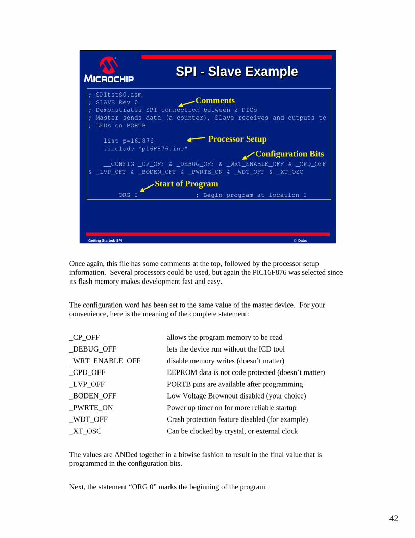
Once again, this file has some comments at the top, followed by the processor setup information. Several processors could be used, but again the PIC16F876 was selected since its flash memory makes development fast and easy.
The configuration word has been set to the same value of the master device. For your convenience, here is the meaning of the complete statement:
_CP_OFF allows the program memory to be read
_DEBUG_OFF lets the device run without the ICD tool
_WRT_ENABLE_OFF disable memory writes (doesn’t matter)
_CPD_OFF EEPROM data is not code protected (doesn’t matter)
_LVP_OFF PORTB pins are available after programming
_BODEN_OFF Low Voltage Brownout disabled (your choice)
_PWRTE_ON Power up timer on for more reliable startup
_WDT_OFF Crash protection feature disabled (for example)
_XT_OSC Can be clocked by crystal, or external clock
The values are ANDed together in a bitwise fashion to result in the final value that is programmed in the configuration bits.
Next, the statement “ORG 0” marks the beginning of the program.
43
Getting Started: SPI © Date:
SPI - Slave ExampleSPI SPI -- Slave ExampleSlave Example
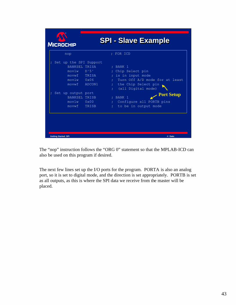
nop ; FOR ICD
; Set up the SPI SupportBANKSEL TRISA ; BANK 1movlw D'5' ; Chip Select pinmovwf TRISA ; is in input modemovlw 0x06 ; Turn Off A/D mode for at leastmovwf ADCON1 ; the Chip Select pin
; (all Digital mode); Set up output port
BANKSEL TRISB ; BANK 1movlw 0x00 ; Configure all PORTB pins movwf TRISB ; to be in output mode
Port Setup
The “nop” instruction follows the “ORG 0” statement so that the MPLAB-ICD can also be used on this program if desired.
The next few lines set up the I/O ports for the program. PORTA is also an analog port, so it is set to digital mode, and the direction is set appropriately. PORTB is set as all outputs, as this is where the SPI data we receive from the master will be placed.
44
Getting Started: SPI © Date:
SPI - Slave ExampleSPI SPI -- Slave ExampleSlave Example
; Set up the SPIBANKSEL TRISC ; BANK 1movlw B'00011000' ; SCK is input (Slave), SDI ismovwf TRISC ; input, SDO is output, all
; others output
movlw B'01000000' ; SPI with middle ofmovwf SSPSTAT ; output time sampling
BANKSEL SSPCON ; BANK 0movlw B'00110100' ; Mode 1,1 SPI Slave Mode,
; Slave Select Requiredmovwf SSPCON ; SSP is on
Set I/O direction for SPI
SPI Configuration
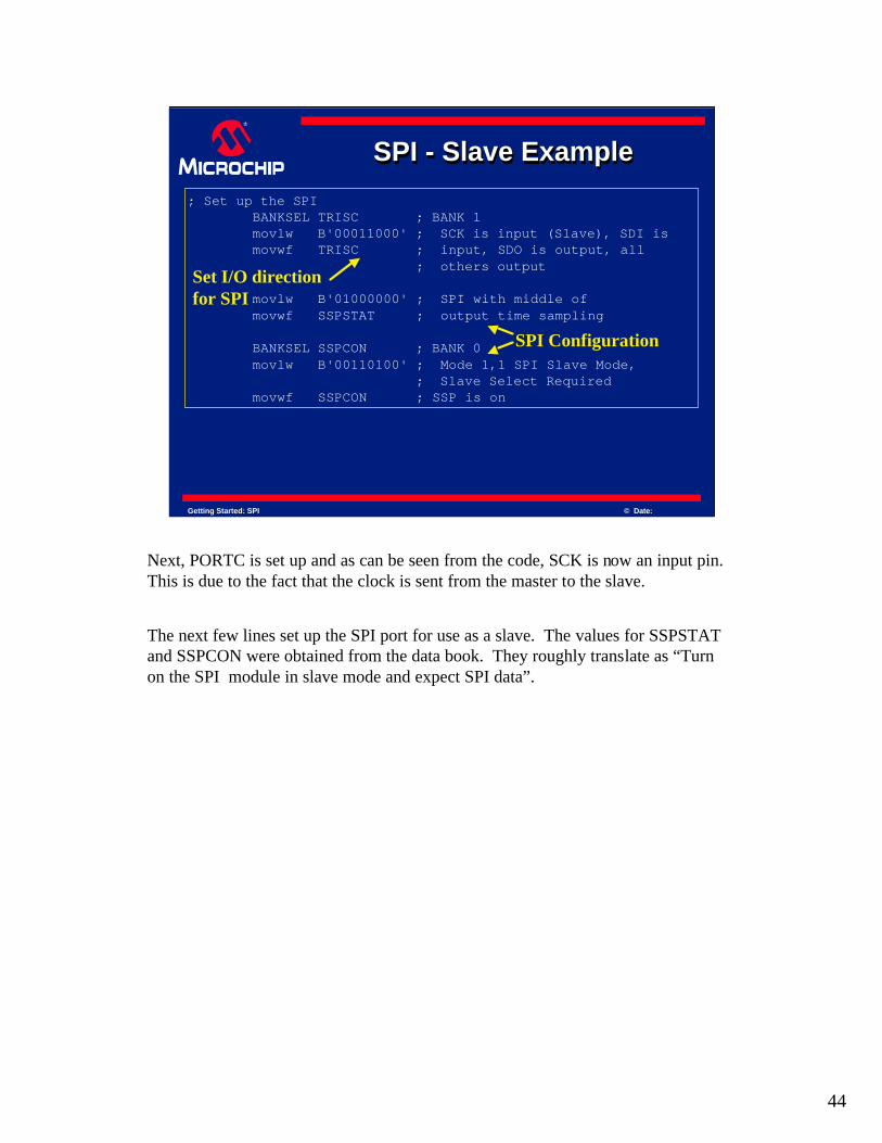
Next, PORTC is set up and as can be seen from the code, SCK is now an input pin. This is due to the fact that the clock is sent from the master to the slave.
The next few lines set up the SPI port for use as a slave. The values for SSPSTAT and SSPCON were obtained from the data book. They roughly translate as “Turn on the SPI module in slave mode and expect SPI data”.
45
Getting Started: SPI © Date:
SPI - Slave ExampleSPI SPI -- Slave ExampleSlave Example
Chk4Dat movlw SSPSTAT ; Indirectly test movwf FSR ; a register by loading FSRbtfss INDF,BF ; Here is the testgoto Chk4Dat ; New data, do a transfer
RX_Data BANKSEL SSPBUF ; BANK 0movf SSPBUF,W ; put in SSPBUF into WBANKSEL PORTB ; BANK 0movwf PORTB ; Show the results on PORTB
DoAgain; Optional customer code can go heregoto Chk4Dat ; Receive Next Byte
END
Check Flag
Read and Display Data
Go to Transfer More DataEnd of Program
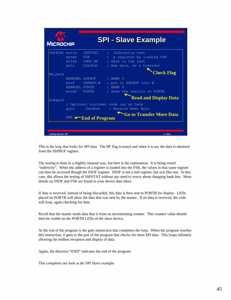
This is the loop that looks for SPI data. The BF flag is tested and when it is set, the data is obtained from the SSPBUF register.
The testing is done in a slightly unusual way, but here is the explanation. It is being tested “indirectly”. When the address of a register is loaded into the FSR, the values in that same register can then be accessed though the INDF register. INDF is not a real register, but acts like one. In this case, this allows the testing of SSPSTAT without any need to worry about changing bank bits. More details on INDF and FSR are found in your device data sheet.
If data is received, instead of being discarded, this data is then sent to PORTB for display. LEDs placed on PORTB will show the data that was sent by the master. If no data is received, the code will loop, again checking for data.
Recall that the master sends data that is from an incrementing counter. This counter value should then be visible on the PORTB LEDs of the slave device.
At the end of the program is the goto instruction that completes the loop. When the program reaches this instruction, it goes to the part of the program that checks for more SPI data. This loops infinitely allowing the endless reception and display of data.
Again, the directive “END” indicates the end of the program.
This completes our look at the SPI Slave example.
46
Getting Started: SPI © Date:
SPI - For More InformationSPI SPI -- For More InformationFor More Information
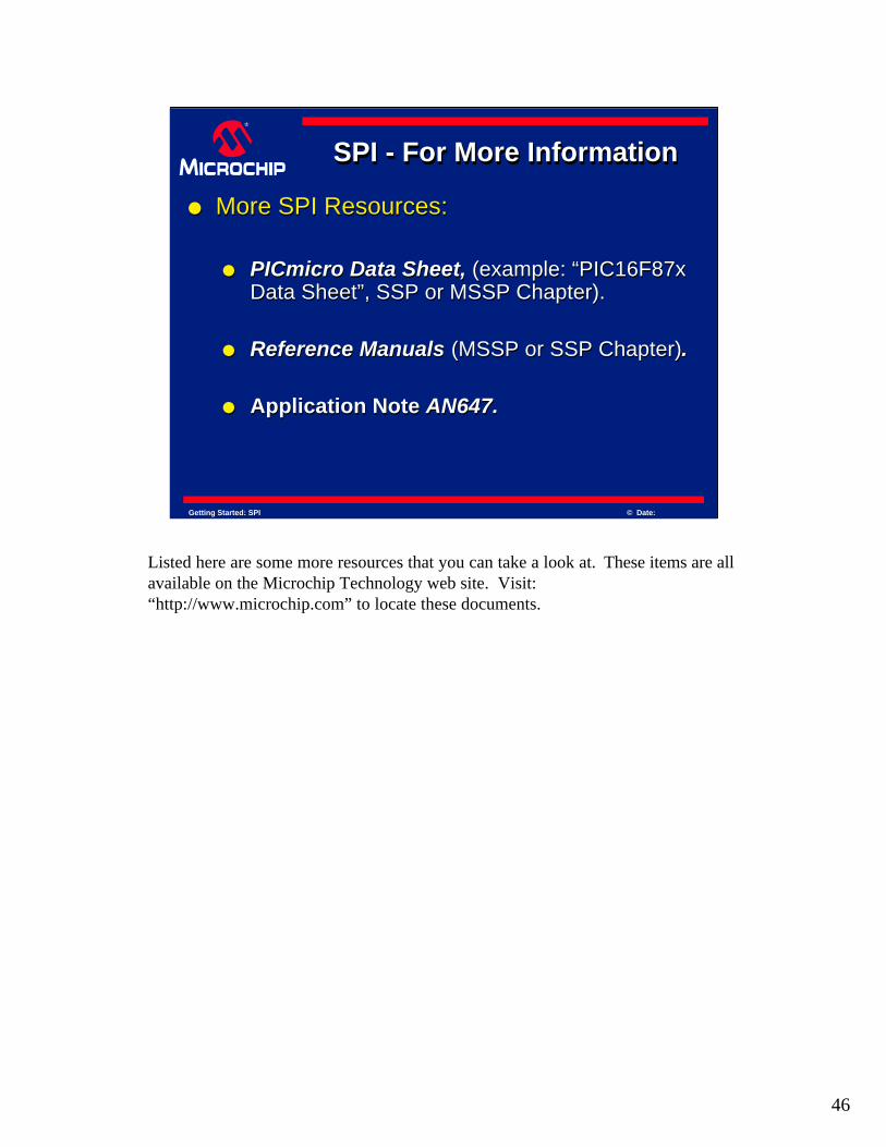
l More SPI Resources:
l PICmicro Data Sheet, (example: “PIC16F87x Data Sheet”, SSP or MSSP Chapter).
l Reference Manuals (MSSP or SSP Chapter).
l Application Note AN647.
l More SPI Resources:
l PICmicro Data Sheet, (example: “PIC16F87x Data Sheet”, SSP or MSSP Chapter).
l Reference Manuals (MSSP or SSP Chapter).
l Application Note AN647.
Listed here are some more resources that you can take a look at. These items are all available on the Microchip Technology web site. Visit: “http://www.microchip.com” to locate these documents.