
FYP II Dissertation BCD Multiplier Ahmed Kamal Saad ...
48
FYP II Dissertation BCD Multiplier Ahmed Kamal Saad Fathallah Abulinain 14708 Electrical and Electronics Engineering Supervisor: Lo Hai Hiung brought to you by CORE View metadata, citation and similar papers at core.ac.uk provided by UTPedia
Transcript of FYP II Dissertation BCD Multiplier Ahmed Kamal Saad ...
FYP II Dissertation
BCD Multiplier
Ahmed Kamal Saad Fathallah Abulinain
14708
Electrical and Electronics Engineering
Supervisor:
Lo Hai Hiung
brought to you by COREView metadata, citation and similar papers at core.ac.uk
provided by UTPedia

1
Table of Contents
CHAPTER 1: ABSTRACT ................................................................................................... 3
CHAPTER 2: INTRODUCTION .......................................................................................... 4
Background ........................................................................................................................ 4
Problem Statement ............................................................................................................. 5
Objective and Scope of Study ............................................................................................ 5
CHAPTER 3: LITERATURE REVIEW AND/OR THEORY .............................................. 7
CHAPTER 4: METHODOLOGY/PROJECT WORK ........................................................ 10
Project Outline ................................................................................................................. 10
Research Steps ................................................................................................................. 10
Comparison Methodology................................................................................................ 11
CHAPTER 5: RESULTS AND DISCUSSION ................................................................... 12
Initial results ..................................................................................................................... 12
Final results ...................................................................................................................... 15
Proposed BCD Multiplier ................................................................................................ 18
o Partial Products of 2 4-bit BCD numbers .................................................................... 19
o Elimination of the Number of Additions ..................................................................... 20
o BCD Addition .............................................................................................................. 22
o Comparison with Previous Designs ............................................................................. 22
CHAPTER 6: CONCLUSION AND RECOMMENDATION ............................................ 24
REFERENCES .................................................................................................................... 25
APPENDICES ..................................................................................................................... 27
Proposed Design Verilog Code ........................................................................................ 27
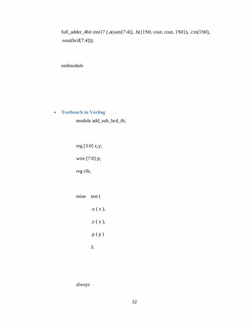
Testbench in Verilog ........................................................................................................ 32
Tested design no. 1 .......................................................................................................... 34
Tested design no. 2 .......................................................................................................... 37
Tested design no. 3 .......................................................................................................... 38
Tested design no. 4 .......................................................................................................... 43

2
List of Figures
Figure 1: Area-optimized binary product BCD digit multiplier, FA (HA): full (half)
adder ................................................................................................................................... 7
Figure 2: Single digit BCD multiplier with further improvements in delay and area........ 8
Figure 3 Comparison between Vedic BCD Multiplier and Previously............................ 12
Figure 4: Modelsim Simulation of BCD Multiplier ......................................................... 14
Figure 5: Area .................................................................................................................. 15
Figure 6: Propagation delay ............................................................................................. 16
Figure 7: Power ................................................................................................................ 17
Figure 8 Binary Partial Products ...................................................................................... 19
Figure 9 Binary-to-BCD conversion ................................................................................ 19
Figure 10 BCD Partial Products ....................................................................................... 20
Figure 11 Minimized BCD Partial Products .................................................................... 21
Figure 12 Comparison with previous designs .................................................................. 23

3
CHAPTER 1: ABSTRACT
BCD multipliers are the basis of accurate decimal multiplication used in
banking systems, scientific calculations, etc. Fractions convert poorly into
binary numbers giving rise to conversion error. Therefore, banking
industry have been using Binary Coded Decimal numbering system for
their banking business transaction to circumvent the error between
decimal fraction number to binary. Here we will explore some single-
digit Binary Coded Decimal Multiplication units that perform
multiplication in hardware for the purpose of future implementation. We
will review existing BCD multipliers and compare them with regard to
their speed, area, power saving and complexity (ability to expand). We
will also propose a design of a BCD multiplier. This is done on Altera
DE2-70 board. All the findings and measurements should be catered
towards that device. The simulations are done using Quartus II software.
This project presents a novel single-digit BCD multiplier that uses a BCD
adder to add the partial products. It distributes the weights of a binary
multiplication to equivalent BCD weights and then adds them. The fact
that only number from 0 to 9 can be used, is manipulated in order to
minimize the number of additions required..
4
CHAPTER 2: INTRODUCTION
Background
When decimal numbers are converted into the conventional binary
numbering system, there is usually a slight conversion error. This
happens because the base of decimal numbers is 10 but the base for
binary numbers is 2. Therefore, it is practically impossible to represent
some particular decimal numbers in binary representations no matter how
many bit we use, there will always be a conversion error no matter how
slight [1].
As an example, if we want to represent the number 0.1 in binary floating-
point, we get 1.00000001490116119384765625E-1 instead of getting 0.1
as the intention was [2].
Another system that can be used to accurately represent numbers in
binary is BCD (Binary-Coded Decimal). It basically allows representing
each decimal number in a chunk of four binary bits. However, this
discards 6 possible combinations of each chunk of four bits, since it only
allows number from 0 to 9.
There are a few possible ways to represent numbers which have a
decimal point in them; fixed-point and floating-point. Fixed point is a
number representation that has a fixed place for the decimal point. For
instance, the number 2.43 has a decimal point 2 places from the right.
This is a restriction and it cannot be changed. That means a number with
3 numbers to the right has to be rounded off to only 2. However floating
point allows the decimal point to move around. In this article, both will
be discussed.
5
Single-digit BCD multipliers are those multipliers which multiply 2 4-bit
numbers and give as an output a single 8-bit (2 digit) number. For
instance; 2 * 8 = 16 which would be 0010 * 1000 = 0001 0110. In this
study we will only be concerned with single-digit BCD multipliers as a
foundation for all implementations.
Problem Statement
As discussed before, it is impossible to represent decimal numbers
accurately when using the conventional floating-point binary
representation. This doesn’t create an issue for commercial usages where
that type of accuracy is negligible.
But for systems such as banking systems and other fields, that accuracy is
needed since a slight conversion error in a small number can result in
misleading calculations which need to be avoided. This can usually be
solved using higher-level programming libraries [3]. However, this is an
inefficient way since it uses a lot of unnecessary calculations that slow
down the system.
This can also create a problem where accurate scientific formulas need to
be computed and simulated for instance where a lot of computing power
shouldn’t be wasted on high-level computations.
Moreover, the inaccuracy escalates when numbers are multiplied.
Therefore, a new system is needed where numbers can be represented
accurately and still hold that accuracy when multiplied.
Objective and Scope of Study
The objective of this study is solve this inaccuracy problem by studying
existing multipliers which use the BCD system and comparing them in
relation to their speed, complexity, power saving and area.

6
Based on that, a BCD multiplier system for banking applications is to be
improved and developed based on the previous aspects. It is to be tested
and implemented on an FPGA (ALTERA DE-2 Kit) for verification
purposes.
Since the foundation of all multipliers is single-digit multipliers, we will
only compare single-digit multipliers developed within the previous 5
years.
The study is customized for banking systems. However, the ability to
expand it for other applications will be taken into consideration so that it
can be used in different fields and applications.
7
CHAPTER 3: LITERATURE REVIEW AND/OR THEORY
The need and popularity of decimal arithmetic has increased recently
since the computational power is needed and the need to eliminate the
high-level arithmetic computations has increased [4]. It has been found
that some applications take up to 90% of their processing time in high-
level arithmetic computing [4]. This is a huge sacrifice of processing
power. BCD systems have recently been more popular in commercialized
processors [5].
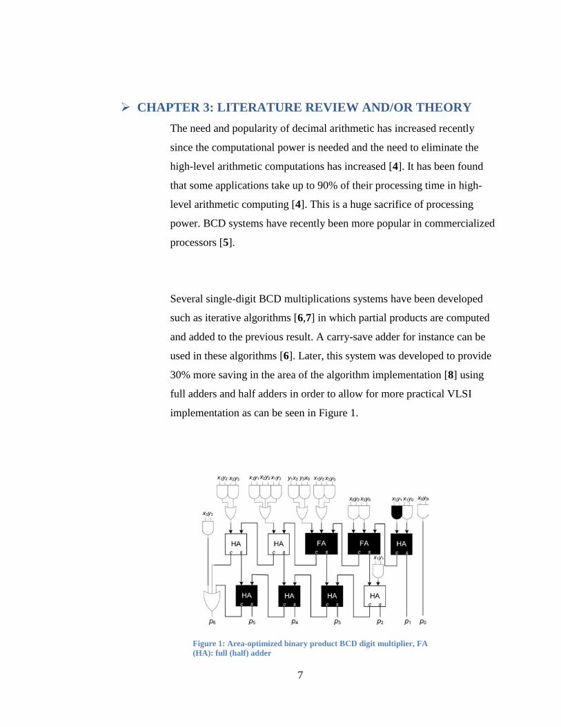
Several single-digit BCD multiplications systems have been developed
such as iterative algorithms [6,7] in which partial products are computed
and added to the previous result. A carry-save adder for instance can be
used in these algorithms [6]. Later, this system was developed to provide
30% more saving in the area of the algorithm implementation [8] using
full adders and half adders in order to allow for more practical VLSI
implementation as can be seen in Figure 1.
Figure 1: Area-optimized binary product BCD digit multiplier, FA
(HA): full (half) adder
8
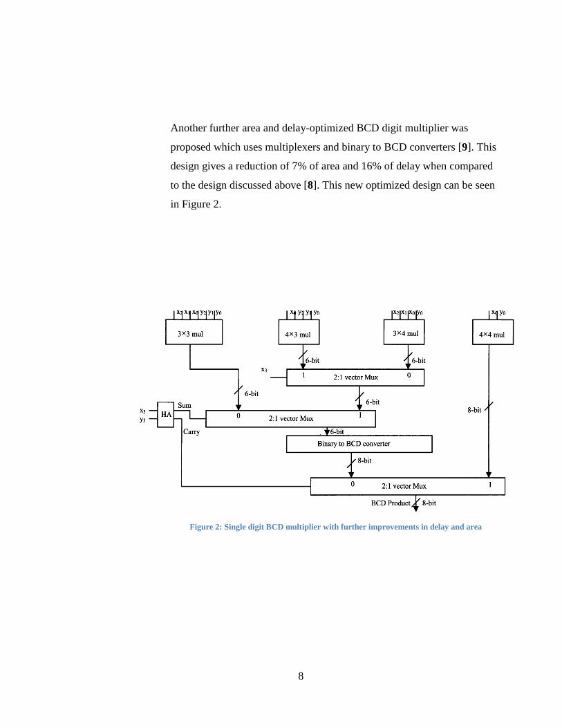
Another further area and delay-optimized BCD digit multiplier was
proposed which uses multiplexers and binary to BCD converters [9]. This
design gives a reduction of 7% of area and 16% of delay when compared
to the design discussed above [8]. This new optimized design can be seen
in Figure 2.
Figure 2: Single digit BCD multiplier with further improvements in delay and area

9
This particular single-digit BCD multiplier was also tested for expansions
such as; multi-digit multiplier as well as fixed-point multiplier [9].
Another expansion [10] was done based on fast partial product generation,
BCD recoding schemes and a BCD-4221 Carry Save Adder reduction tree
[11]. This expansion is an FPGA implementation of decimal floating-
point achieved with a parallel fixed-point multiplier in order to comply
with IEEE 754-2008 [12] which is the IEEE approved standard for
decimal floating-point arithmetic.

10
CHAPTER 4: METHODOLOGY/PROJECT WORK
Project Outline
Key Milestone Process
Research Steps
1. Write the verilog code of the design using Quartus II software
2. Test the code on the DE2-70 kit to make sure it’s working
3. Simulate the code using modelsim
4. Take the measurements:
a. Area (number of elements used)
b. Power
c. Speed (maximum propagation delay)
5. Deciding how easy it is to expand the multiplier
6. Repeating the above steps for each design used
7. Propose a new design.
11
Comparison Methodology
The methodology used in comparison is heavily based on implementation
on Altera FPGA DE2-70 board. First the designs are to be simulated for
functionality purposes. This is done using Modelsim. Later on, Quartus II
software is used to determine the size of the design on the actual board
and the result is used for area saving comparisons. Quartus II is also used
to determine the power the design uses. And based on the power
consumption and the area saving, the cost will be calculated since it
varies accordingly. The area is also determined using the number of
elements used.
12
CHAPTER 5: RESULTS AND DISCUSSION
Initial results
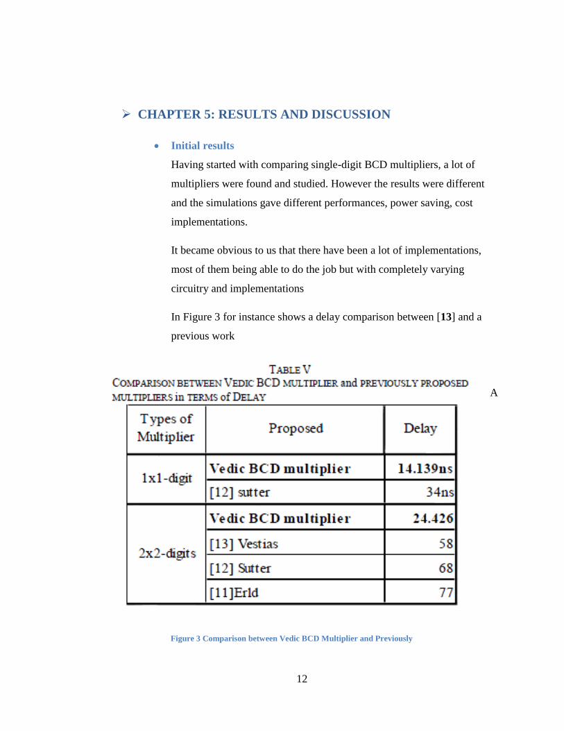
Having started with comparing single-digit BCD multipliers, a lot of
multipliers were found and studied. However the results were different
and the simulations gave different performances, power saving, cost
implementations.
It became obvious to us that there have been a lot of implementations,
most of them being able to do the job but with completely varying
circuitry and implementations
In Figure 3 for instance shows a delay comparison between [13] and a
previous work
A
Figure 3 Comparison between Vedic BCD Multiplier and Previously

13
Furthermore a mistake in a formula was found and referenced in [8]. That
mistake being if we try and multiply 5 x 1 using the formula in [6] we get
an incorrect result of 1 instead of 5.
This particular mistake shows that all data needs to verified and simulated
properly before anything is to be assumed. However, all other formulas
and algorithms that were tested show correct behavior.
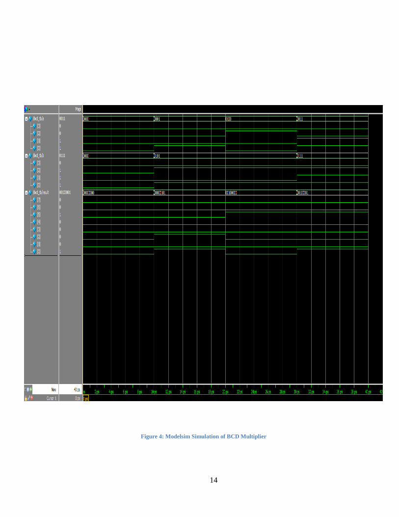
A testbench was developed and used to test a number of the designs of
single-digit mentioned in the literature review. All results came
conforming with the functionality of the BCD multipliers. Figure 4 shows
the input vectors (a, b) and the output (result) from the designs tested. All
designs conformed with the expected results. When a is 0 (000) and b is 0
(000) the result is (0000 0000). When a is 1 (0001) and b is 5 (0101), the
result is 5 (0000 0101). When a is 4 (0100) and b is 5 (0101), the result is
20 (0010 0000). When a is 3 (0011) and b is 7 (0111), the result is 21
(0010 0001).
This is the basic behavior testing of the BCD multiplier. In the test
vectors, there were some of them that differentiate between a normal
multiplier and a BCD multiplier and the result confirms with the
functionality that a BCD multiplier has
14
Figure 4: Modelsim Simulation of BCD Multiplier
15
Final results
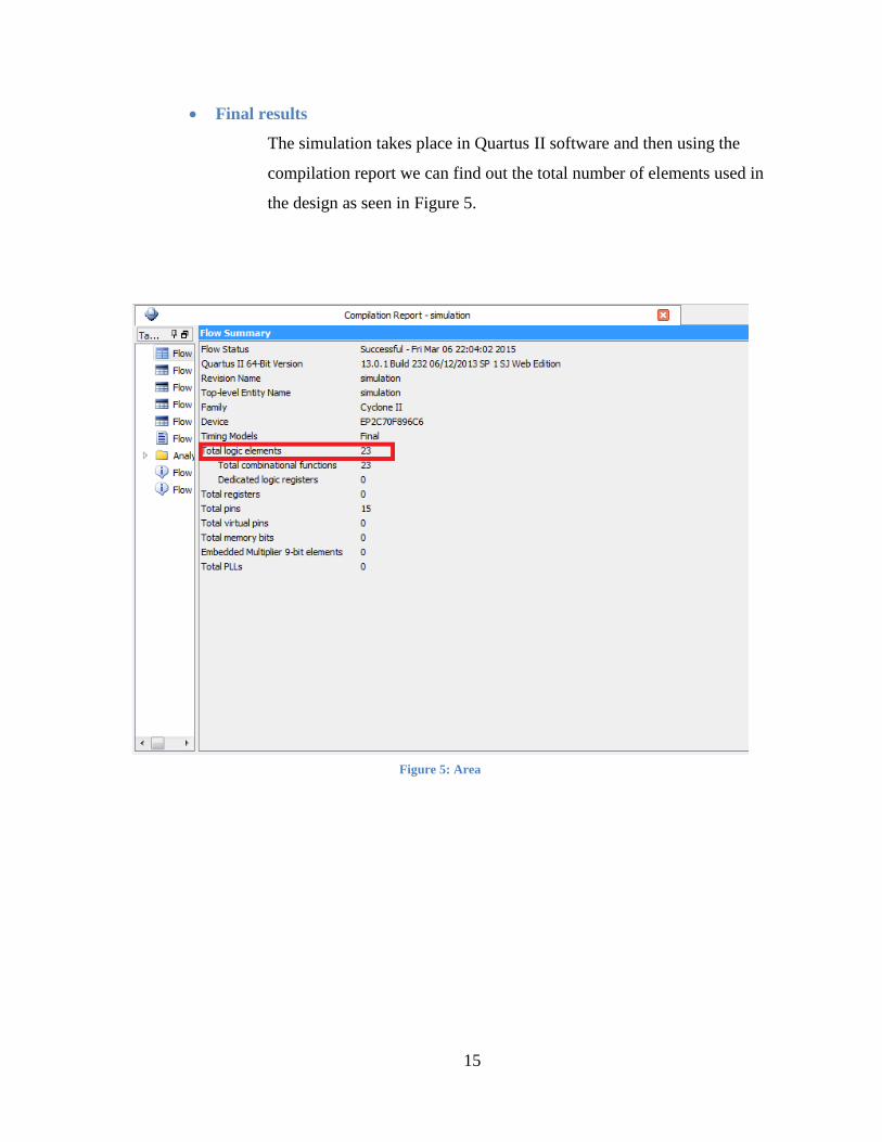
The simulation takes place in Quartus II software and then using the
compilation report we can find out the total number of elements used in
the design as seen in Figure 5.
Figure 5: Area
16
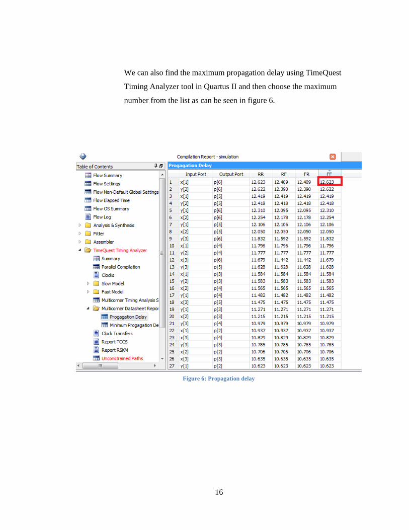
We can also find the maximum propagation delay using TimeQuest
Timing Analyzer tool in Quartus II and then choose the maximum
number from the list as can be seen in figure 6.
Figure 6: Propagation delay
17
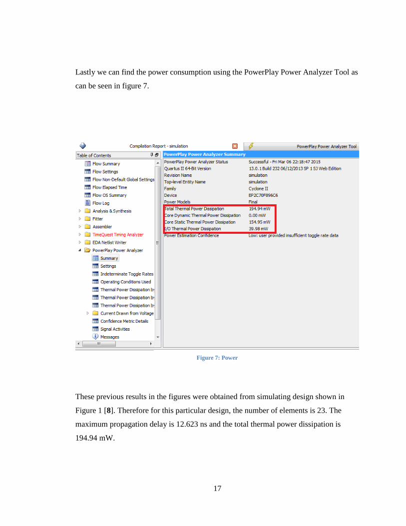
Lastly we can find the power consumption using the PowerPlay Power Analyzer Tool as
can be seen in figure 7.
These previous results in the figures were obtained from simulating design shown in
Figure 1 [8]. Therefore for this particular design, the number of elements is 23. The
maximum propagation delay is 12.623 ns and the total thermal power dissipation is
194.94 mW.
Figure 7: Power

18
Proposed BCD Multiplier
Based on the research done and the results from the simulations, a BCD
multiplier was designed which has small delay and area calculations.
The idea of the BCD multiplier is based on a normal binary multiplier
that uses an adder to add the individual partial products. However, the
weights are distributed differently to suit a BCD multiplier. The adder
integrated also is a BCD adder instead of a binary adder.
The BCD adder adds 2 8-bit number by adding each 4-bit combination
and checking if the number is larger than 9. If so, then it adds 6 to the
existing result.
The weights of the BCD multiplier were arranged so that it achieves
maximum speed and minimum area.
The end result was that the multiplier adds only 4 8-bit BCD numbers
resulting in only 3 BCD adders with an area of 50 and a delay of almost
18 ns.
This is very comparable to the results above since the previous results are
based on multipliers that give the output in binary which would require
BCD conversion which makes the data here less accurate.
Below are the details of this new proposed multiplier.
19
o Partial Products of 2 4-bit BCD numbers
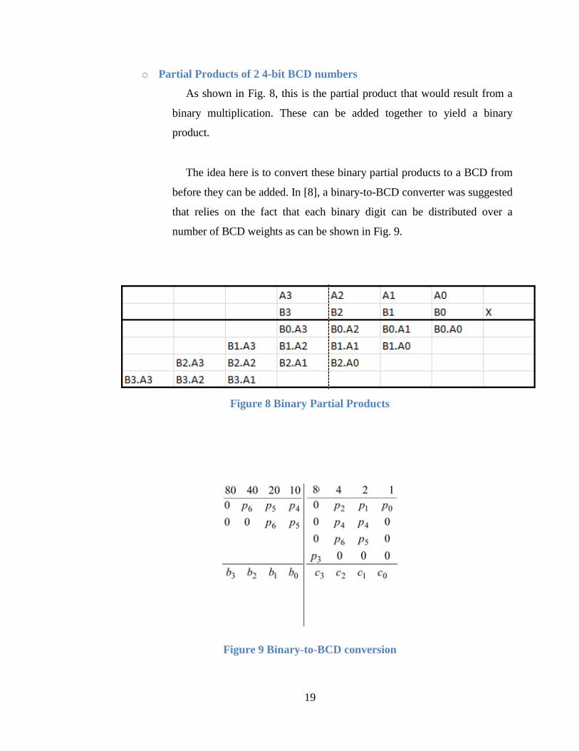
As shown in Fig. 8, this is the partial product that would result from a
binary multiplication. These can be added together to yield a binary
product.
The idea here is to convert these binary partial products to a BCD from
before they can be added. In [8], a binary-to-BCD converter was suggested
that relies on the fact that each binary digit can be distributed over a
number of BCD weights as can be shown in Fig. 9.
Figure 8 Binary Partial Products
Figure 9 Binary-to-BCD conversion
20
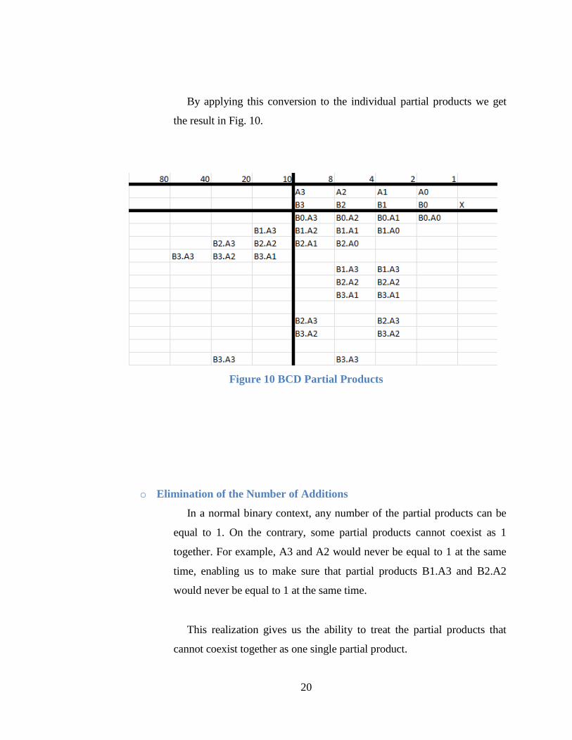
By applying this conversion to the individual partial products we get
the result in Fig. 10.
Figure 10 BCD Partial Products
o Elimination of the Number of Additions
In a normal binary context, any number of the partial products can be
equal to 1. On the contrary, some partial products cannot coexist as 1
together. For example, A3 and A2 would never be equal to 1 at the same
time, enabling us to make sure that partial products B1.A3 and B2.A2
would never be equal to 1 at the same time.
This realization gives us the ability to treat the partial products that
cannot coexist together as one single partial product.
21
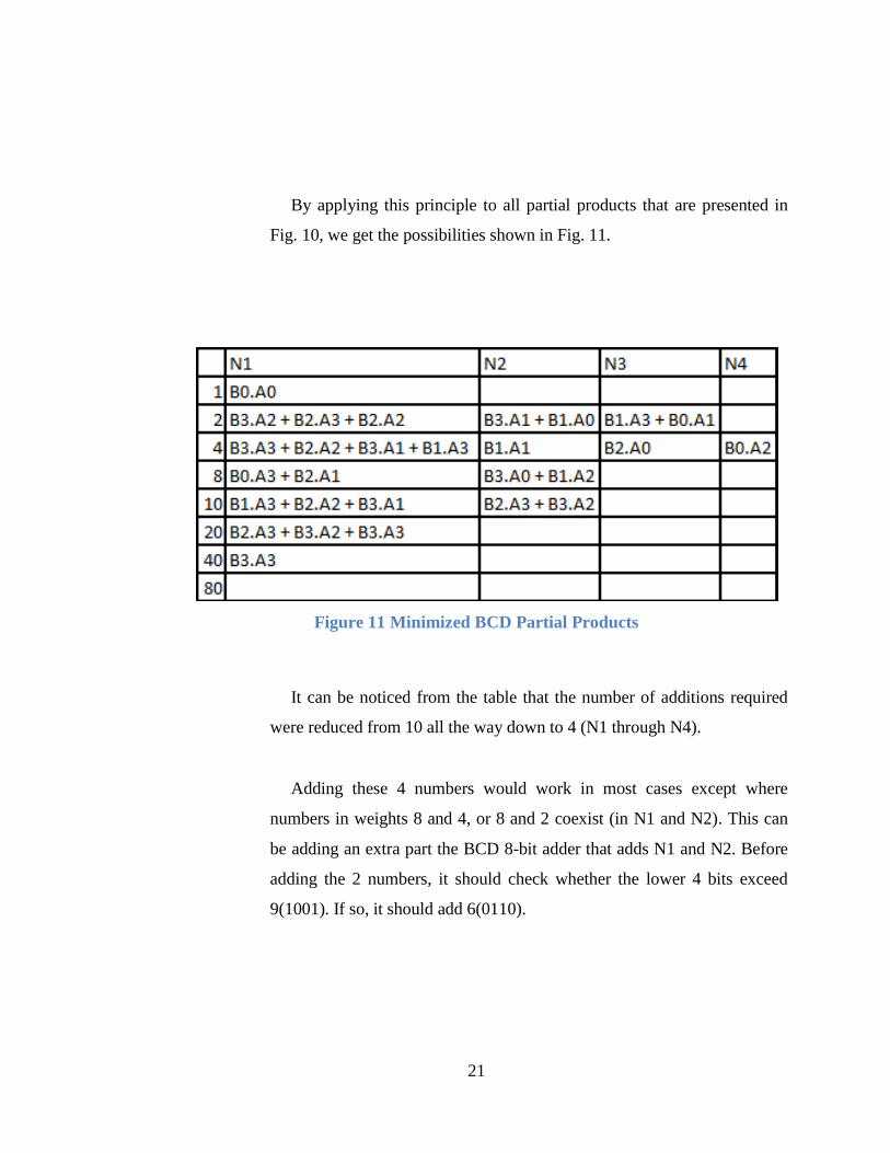
By applying this principle to all partial products that are presented in
Fig. 10, we get the possibilities shown in Fig. 11.
Figure 11 Minimized BCD Partial Products
It can be noticed from the table that the number of additions required
were reduced from 10 all the way down to 4 (N1 through N4).
Adding these 4 numbers would work in most cases except where
numbers in weights 8 and 4, or 8 and 2 coexist (in N1 and N2). This can
be adding an extra part the BCD 8-bit adder that adds N1 and N2. Before
adding the 2 numbers, it should check whether the lower 4 bits exceed
9(1001). If so, it should add 6(0110).

22
o BCD Addition
A number of BCD adders have been addressed. However, here a simple
adder that adds the 2 numbers and then checks if the number is larger than
9. If it is, then the adder adds 6 to the existing number [14]
The individual binary adders used inside are simple 4-bit ripple-carry
adders in order to reduce the area.
A simple equation is used to check if the output of one 4-bit adder
exceeds 9.
E = Sum[1].Sum[3] + Sum[2].Sum[3]
o Comparison with Previous Designs
This design and other designs were synthesized using Quartus II
software with a target device of Cyclone II EP2C70F896C6 of Altera
DE2-70 Kit. The parameters that were acquired are; area, delay and power
consumption.
Some of the designs generate a binary output which would greatly
reduce the area and the delay.
The results are shown in Fig. 12.
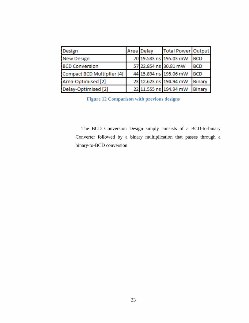
23
Figure 12 Comparison with previous designs
The BCD Conversion Design simply consists of a BCD-to-binary
Converter followed by a binary multiplication that passes through a
binary-to-BCD conversion.

24
CHAPTER 6: CONCLUSION AND RECOMMENDATION
A few designs have been explored and studied starting with single-digit
BCD multipliers. These were extended to multi-digit BCD multipliers
and later into fixed-point implementations. Floating-point multipliers
were built upon that which comply with IEEE 754-2008 [12].
The single-digit multipliers are to be studied and compared in regard to
their cost, power saving, complexity, area and speed. The 2-semester plan
was discussed with the goal of publishing a paper containing the results
of the simulations.
The initial results were discussed and it was shown how important the
simulations and verifications are.
It was also shown how the methodology is planned to be implemented
using Quartus II to provide the results of speed, power and area.
The future works were illustrated and explained for consistency with the
rest of the 2-semester plan
25
REFERENCES
[1] (2005, August) Microsoft. [Online]. http://support.microsoft.com/kb/42980
[2] David Goldberg, "What Every Computer Scientist Should Know About Floating-
Point Arithmetic," 1991.
[3] (2014, May) Floating Point Currency. [Online].
http://c2.com/cgi/wiki?FloatingPointCurrency
[4] Michael F. Cowlishaw, "Decimal Floating-Point: Algorism for Computers," IEEE,
June 2003.
[5] F.Y., Krygowski, C.A., Li, W.H., Schwarz, E.M., and Carlough, S.R. Busaba, "The
IBM Z900 decimal arithmetic unit," November 2001.
[6] M.A., and Schulte, M.J. Erle, "Decimal multiplication via carry-save".
[7] M.A., Schwartz, E.M., and Schulte, M.J. Erle, "Decimal multiplication with
efficient partial product generation," June 2005.
[8] G. Jaberipur and A. Kaivani, "Binary-coded decimal digit multipliers," July 2007.
[9] SHAHANA T. K, K. POULOSE JACOB, SREELASASI REKHA K. JAMES,
"Decimal Multiplication using compact BCD Multiplier," December 2008.
[10] Thomas Teufel Malte Baesler, "FPGA Implementation of a Decimal Floating-Point
Accurate Scalar Product Unit," 2009.
[11] E. Antelo, and P. Montuschi A. Vazquez, "A new family of high-performance
parallel decimal multipliers," June 2007.
[12] IEEE, "IEEE 754-2008 Standard for Floating-Point Arithmetic," September 2008.

26
[13] Mukesh Gupta, Vipin Jain, udhir kumar Arvind Kumar Mehta, "High Performance
Vedic BCD Multiplier and Modified Binary to BCD Converter," IEEE, 2013.
[14] Joseph Cavanagh, Verilog HDL Digital Design and Modeling, 2007, ch. 11, pp.
669-685.

27
APPENDICES
Proposed Design Verilog Code
module mine(
input [3:0] x,
input [3:0] y,
output [7:0] p
);
wire [7:0] a1 = {1'b0, x[3]&y[3], x[2]&y[3] | x[3]&y[2] | x[3]&y[3], x[1]&y[3] |
x[2]&y[2] | x[3]&y[1], x[0]&y[3] | x[2]&y[1], x[3]&y[3] | x[2]&y[2] | x[3]&y[1]
| x[1]&y[3], x[3]&y[2] | x[2]&y[3] | x[2]&y[2], x[0]&y[0]};
wire [7:0] a2 = {3'b0, x[2]&y[3] | x[3]&y[2], x[3]&y[0] | x[1]&y[2], x[1]&y[1],
x[3]&y[1] | x[1]&y[0], 1'b0};
wire [7:0] a3 = {5'b0, x[2]&y[0], x[1]&y[3] | x[0]&y[1], 1'b0};
wire [7:0] a4 = {5'b0, x[0]&y[2], 2'b0};
wire [7:0] net1, net2;
bcd_adder_2 inst1(.a_i(a1), .b_i(a2), .bcd(net1));
bcd_adder inst2(.a(net1), .b(a3), .bcd(net2));
bcd_adder inst3(.a(net2), .b(a4), .bcd(p));
endmodule
module FA(sout,cout,a,b,cin);
output sout,cout;
28
input a,b,cin;
assign sout=(a^b^cin);
assign cout=((a&b)|(a&cin)|(b&cin));
endmodule
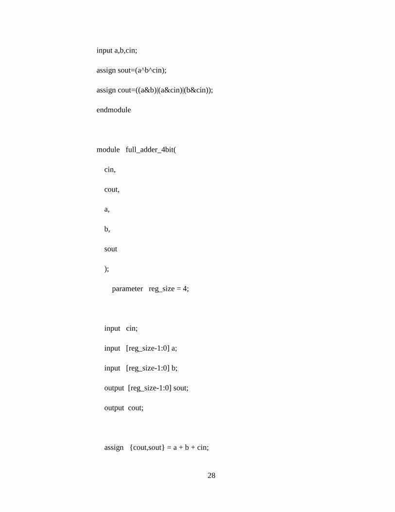
module full_adder_4bit(
cin,
cout,
a,
b,
sout
);
parameter reg_size = 4;
input cin;
input [reg_size-1:0] a;
input [reg_size-1:0] b;
output [reg_size-1:0] sout;
output cout;
assign {cout,sout} = a + b + cin;
29
endmodule
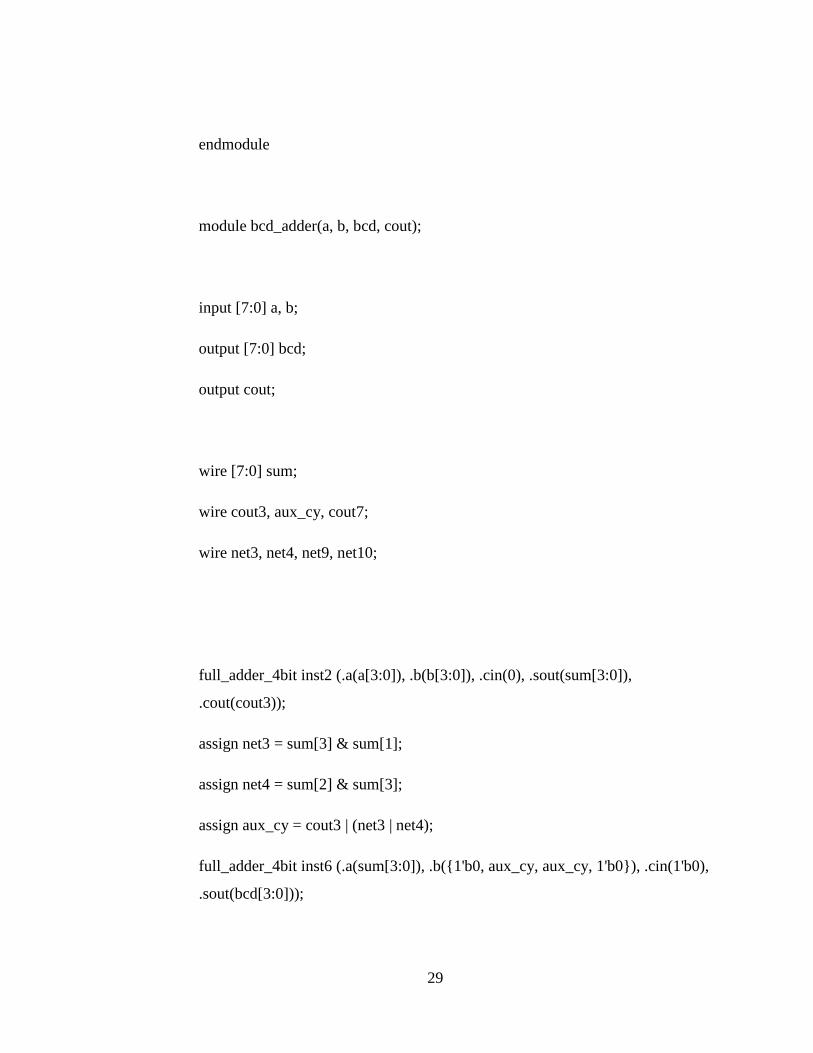
module bcd_adder(a, b, bcd, cout);
input [7:0] a, b;
output [7:0] bcd;
output cout;
wire [7:0] sum;
wire cout3, aux_cy, cout7;
wire net3, net4, net9, net10;
full_adder_4bit inst2 (.a(a[3:0]), .b(b[3:0]), .cin(0), .sout(sum[3:0]),
.cout(cout3));
assign net3 = sum[3] & sum[1];
assign net4 = sum[2] & sum[3];
assign aux_cy = cout3 | (net3 | net4);
full_adder_4bit inst6 (.a(sum[3:0]), .b({1'b0, aux_cy, aux_cy, 1'b0}), .cin(1'b0),
.sout(bcd[3:0]));
30
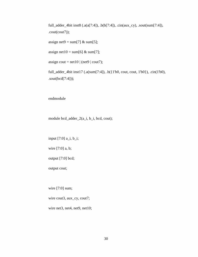
full_adder_4bit inst8 (.a(a[7:4]), .b(b[7:4]), .cin(aux_cy), .sout(sum[7:4]),
.cout(cout7));
assign net9 = sum[7] & sum[5];
assign net10 = sum[6] & sum[7];
assign cout = net10 | (net9 | cout7);
full_adder_4bit inst17 (.a(sum[7:4]), .b({1'b0, cout, cout, 1'b0}), .cin(1'b0),
.sout(bcd[7:4]));
endmodule
module bcd_adder_2(a_i, b_i, bcd, cout);
input [7:0] a_i, b_i;
wire [7:0] a, b;
output [7:0] bcd;
output cout;
wire [7:0] sum;
wire cout3, aux_cy, cout7;
wire net3, net4, net9, net10;
31
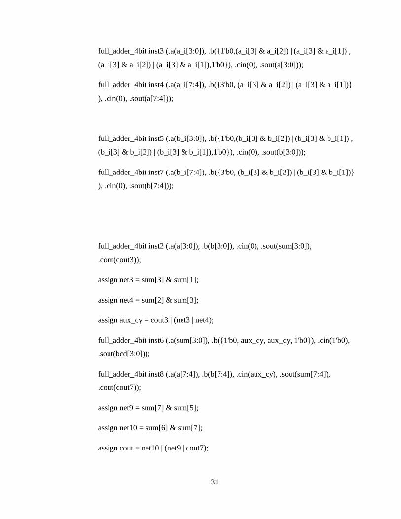
full_adder_4bit inst3 (.a(a_i[3:0]), .b({1'b0,(a_i[3] & a_i[2]) | (a_i[3] & a_i[1]) ,
(a_i[3] & a_i[2]) | (a_i[3] & a_i[1]),1'b0}), .cin(0), .sout(a[3:0]));
full_adder_4bit inst4 (.a(a_i[7:4]), .b({3'b0, (a_i[3] & a_i[2]) | (a_i[3] & a_i[1])}
), .cin(0), .sout(a[7:4]));
full_adder_4bit inst5 (.a(b_i[3:0]), .b({1'b0,(b_i[3] & b_i[2]) | (b_i[3] & b_i[1]) ,
(b_i[3] & b_i[2]) | (b_i[3] & b_i[1]),1'b0}), .cin(0), .sout(b[3:0]));
full_adder_4bit inst7 (.a(b_i[7:4]), .b({3'b0, (b_i[3] & b_i[2]) | (b_i[3] & b_i[1])}
), .cin(0), .sout(b[7:4]));
full_adder_4bit inst2 (.a(a[3:0]), .b(b[3:0]), .cin(0), .sout(sum[3:0]),
.cout(cout3));
assign net3 = sum[3] & sum[1];
assign net4 = sum[2] & sum[3];
assign aux_cy = cout3 | (net3 | net4);
full_adder_4bit inst6 (.a(sum[3:0]), .b({1'b0, aux_cy, aux_cy, 1'b0}), .cin(1'b0),
.sout(bcd[3:0]));
full_adder_4bit inst8 (.a(a[7:4]), .b(b[7:4]), .cin(aux_cy), .sout(sum[7:4]),
.cout(cout7));
assign net9 = sum[7] & sum[5];
assign net10 = sum[6] & sum[7];
assign cout = net10 | (net9 | cout7);
32
full_adder_4bit inst17 (.a(sum[7:4]), .b({1'b0, cout, cout, 1'b0}), .cin(1'b0),
.sout(bcd[7:4]));
endmodule
Testbench in Verilog
module add_sub_bcd_tb;
reg [3:0] x,y;
wire [7:0] p;
reg clk;
mine test (
.x ( x ),
.y ( y ),
.p ( p )
);
always
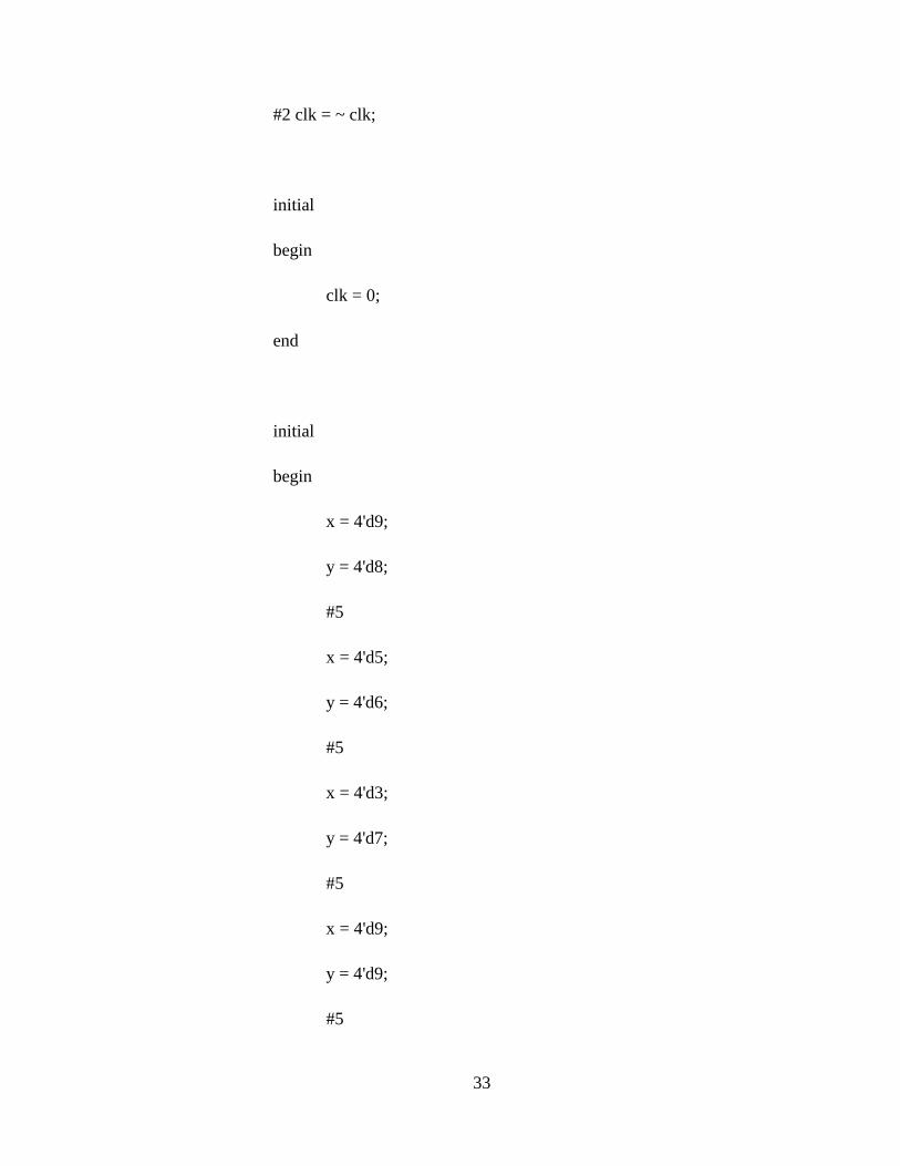
33
#2 clk = ~ clk;
initial
begin
clk = 0;
end
initial
begin
x = 4'd9;
y = 4'd8;
#5
x = 4'd5;
y = 4'd6;
#5
x = 4'd3;
y = 4'd7;
#5
x = 4'd9;
y = 4'd9;
#5
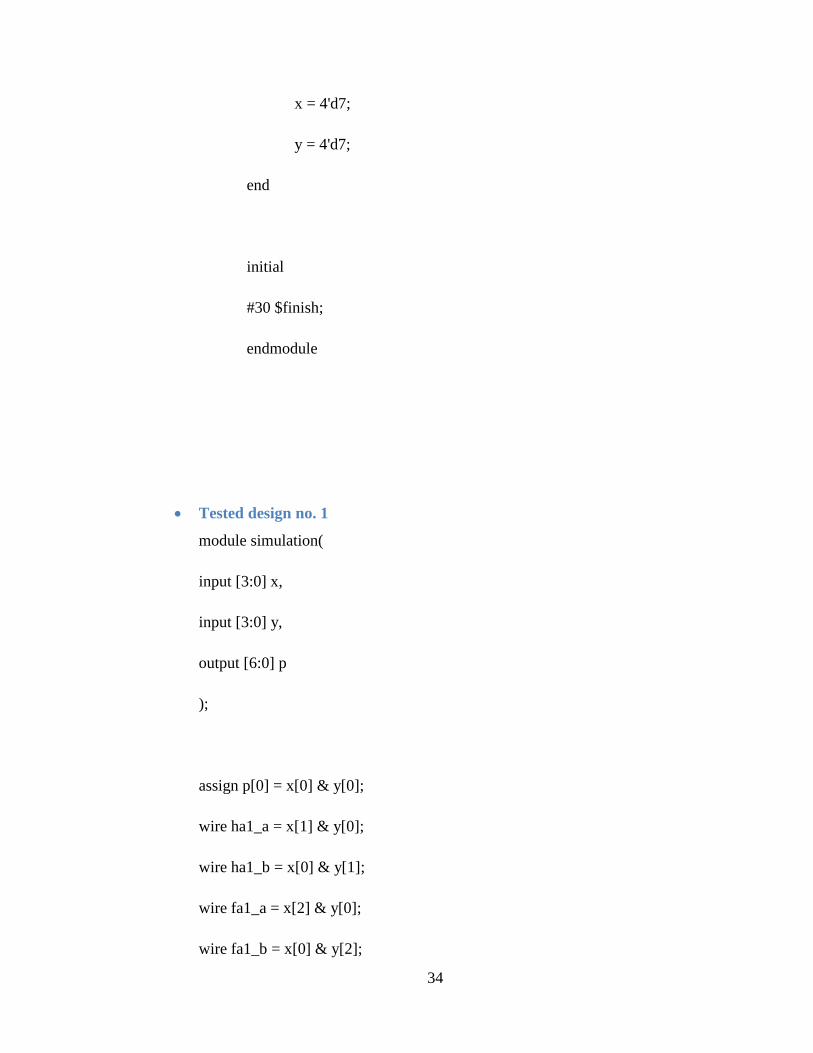
34
x = 4'd7;
y = 4'd7;
end
initial
#30 $finish;
endmodule
Tested design no. 1
module simulation(
input [3:0] x,
input [3:0] y,
output [6:0] p
);
assign p[0] = x[0] & y[0];
wire ha1_a = x[1] & y[0];
wire ha1_b = x[0] & y[1];
wire fa1_a = x[2] & y[0];
wire fa1_b = x[0] & y[2];
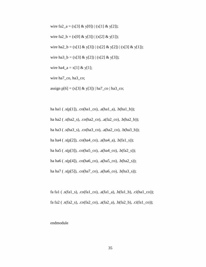
35
wire fa2_a = (x[3] & y[0]) | (x[1] & y[2]);
wire fa2_b = (x[0] & y[3]) | (x[2] & y[1]);
wire ha2_b = (x[1] & y[3]) | (x[2] & y[2]) | (x[3] & y[1]);
wire ha3_b = (x[3] & y[2]) | (x[2] & y[3]);
wire ha4_a = x[1] & y[1];
wire ha7_co, ha3_co;
assign p[6] = (x[3] & y[3]) | ha7_co | ha3_co;
ha ha1 ( .s(p[1]), .co(ha1_co), .a(ha1_a), .b(ha1_b));
ha ha2 ( .s(ha2_s), .co(ha2_co), .a(fa2_co), .b(ha2_b));
ha ha3 ( .s(ha3_s), .co(ha3_co), .a(ha2_co), .b(ha3_b));
ha ha4 ( .s(p[2]), .co(ha4_co), .a(ha4_a), .b(fa1_s));
ha ha5 ( .s(p[3]), .co(ha5_co), .a(ha4_co), .b(fa2_s));
ha ha6 ( .s(p[4]), .co(ha6_co), .a(ha5_co), .b(ha2_s));
ha ha7 ( .s(p[5]), .co(ha7_co), .a(ha6_co), .b(ha3_s));
fa fa1 ( .s(fa1_s), .co(fa1_co), .a(fa1_a), .b(fa1_b), .ci(ha1_co));
fa fa2 ( .s(fa2_s), .co(fa2_co), .a(fa2_a), .b(fa2_b), .ci(fa1_co));
endmodule
36
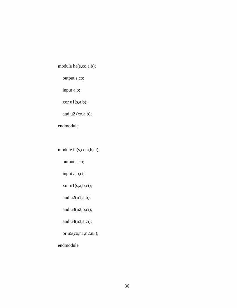
module ha(s,co,a,b);
output s,co;
input a,b;
xor u1(s,a,b);
and u2 (co,a,b);
endmodule
module fa(s,co,a,b,ci);
output s,co;
input a,b,ci;
xor u1(s,a,b,ci);
and u2(n1,a,b);
and u3(n2,b,ci);
and u4(n3,a,ci);
or u5(co,n1,n2,n3);
endmodule

37
Tested design no. 2
module U_04271381(
input [3:0] x,
input [3:0] y,
output [6:0] p
);
assign p[0] = y[0] & x[0];
assign p[1] = (x[0] & y[1]) ^ (x[1] & y[0]) ;
assign p[2] = ( x[0] & y[1] & x[1] & y[0] ) ^ ( x[1] & y[1] ) ^ (x[2] & y[0]) ^ (
x[0] & y[2] );
assign p[3] = ((x[1] & y[2]) | (x[0] & y[3])) ^ ((x[2] & y[1]) | (x[3] & y[0])) ^
((((~y[0]) & (x[0] & y[1]) & ((x[1] & y[2]) | (x[0] & y[3]))) | (((x[1] & y[2]) |
(x[0] & y[3])) & (x[0] & y[1]) & (~x[2])) | ((~x[0]) & (x[1] & y[0]) & ((x[2] &
y[1]) | (x[3] & y[0]))) | ((~x[2]) & (x[1] & y[0]) & ((x[2] & y[1]) | (x[3] &
y[0])))) | ((~x[2]) & ((x[0] & y[1]) & (x[1] & y[0])) & (~x[2])) | ((~x[1]) & (x[2]
& y[0]) & (x[0] & y[2])) | ((x[0] & y[2]) & (x[2] & y[0]) & (~x[1])));
assign p[4] = ((((~y[0]) & (x[0] & y[1]) & ((x[1] & y[2]) | (x[0] & y[3]))) |
(((x[1] & y[2]) | (x[0] & y[3])) & (x[0] & y[1]) & (~x[2])) | ((~x[0]) & (x[1] &
y[0]) & ((x[2] & y[1]) | (x[3] & y[0]))) | ((~x[2]) & (x[1] & y[0]) & ((x[2] &
y[1]) | (x[3] & y[0])))) | (((~y[1]) & (x[0] & y[2]) & (x[2] & y[0]) & (x[1])) |
((x[0] & y[2]) & (x[2] & y[0]) & (~x[1]) & (y[1])) | ((x[1] & y[1]) & (x[2] &
y[2]))) | ((x[3] & y[3]) & (x[0] & y[0]))) ^ (((x[2] & y[0]) & (x[1] & y[1]) &
(x[0] & y[2])) ^ ((x[2] & y[2]) | (x[3] & x[1]) | (x[1] & y[3])));
38
assign p[5] = (((~y[1]) & (x[0] & y[2]) & (x[2] & y[0]) & (x[1])) | ((x[0] & y[2])
& (x[2] & y[0]) & (~x[1]) & (y[1])) | ((x[1] & y[1]) & (x[2] & y[2]))) ^ ((x[3] &
y[2]) | (x[2] & y[3]));
assign p[6] = x[3] & y[3];
endmodule
Tested design no. 3
module U_04786744(
input [3:0] x,
input [3:0] y,
output [7:0] p
);
wire [5:0] mul_33, mul_43, mul_34, mux_1, mux_2;
wire [7:0] mux_3;
wire [7:0] mul_44;
wire [7:0] conv_out;
wire sum, carry;
assign mul_33 = x[2:0] * y[2:0];
39
assign mul_43[0] = x[0] & y[0];
assign mul_43[1] = x[0] & y[1];
assign mul_43[2] = x[0] & y[2];
assign mul_43[3] = y[0];
assign mul_43[4] = y[1];
assign mul_43[5] = y[2];
assign mul_34[0] = x[0] & y[0];
assign mul_34[1] = x[1] & y[0];
assign mul_34[2] = x[2] & y[0];
assign mul_34[3] = x[0];
assign mul_34[4] = x[1];
assign mul_34[5] = x[2];
assign mul_44[0] = x[0] & y[0];
assign mul_44[1] = x[0] ^ y[0];
assign mul_44[2] = ~(x[0] | y[0]);
assign mul_44[3] = 0;
assign mul_44[4] = x[0] ^ y[0];
assign mul_44[5] = ~(x[0] & y[0]);
assign mul_44[6] = ~(x[0] & y[0]);

40
assign mul_44[7] = x[0] & y[0];
ha ha1 (sum, carry, x[3], y[3]);
assign mux_1 = x[3]? mul_43 : mul_34;
assign mux_2 = sum? mux_1 : mul_33;
binary_to_BCD binary_to_BCD1 ({1'b0, mux_2}, conv_out[3:0],
conv_out[7:4]);
assign p = carry? mul_44 : conv_out;
endmodule
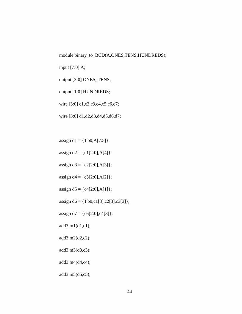
module binary_to_BCD(A,ONES,TENS,HUNDREDS);
input [7:0] A;
output [3:0] ONES, TENS;
output [1:0] HUNDREDS;
wire [3:0] c1,c2,c3,c4,c5,c6,c7;
wire [3:0] d1,d2,d3,d4,d5,d6,d7;
assign d1 = {1'b0,A[7:5]};
41
assign d2 = {c1[2:0],A[4]};
assign d3 = {c2[2:0],A[3]};
assign d4 = {c3[2:0],A[2]};
assign d5 = {c4[2:0],A[1]};
assign d6 = {1'b0,c1[3],c2[3],c3[3]};
assign d7 = {c6[2:0],c4[3]};
add3 m1(d1,c1);
add3 m2(d2,c2);
add3 m3(d3,c3);
add3 m4(d4,c4);
add3 m5(d5,c5);
add3 m6(d6,c6);
add3 m7(d7,c7);
assign ONES = {c5[2:0],A[0]};
assign TENS = {c7[2:0],c5[3]};
assign HUNDREDS = {c6[3],c7[3]};
endmodule
module add3(in,out);
42
input [3:0] in;
output [3:0] out;
reg [3:0] out;
always @ (in)
case (in)
4'b0000: out <= 4'b0000;
4'b0001: out <= 4'b0001;
4'b0010: out <= 4'b0010;
4'b0011: out <= 4'b0011;
4'b0100: out <= 4'b0100;
4'b0101: out <= 4'b1000;
4'b0110: out <= 4'b1001;
4'b0111: out <= 4'b1010;
4'b1000: out <= 4'b1011;
4'b1001: out <= 4'b1100;
default: out <= 4'b0000;
endcase
endmodule
module ha(s,co,a,b);

43
output s,co;
input a,b;
xor u1(s,a,b);
and u2 (co,a,b);
endmodule
Tested design no. 4
module U_05483001(
input [3:0] x,
input [3:0] y,
output [7:0] p
);
wire [7:0] MUL;
multiply4bits mul1 (MUL, x, y);
binary_to_BCD convert1 (.A(MUL), .ONES(p[3:0]), .TENS(p[7:4]));
endmodule
44
module binary_to_BCD(A,ONES,TENS,HUNDREDS);
input [7:0] A;
output [3:0] ONES, TENS;
output [1:0] HUNDREDS;
wire [3:0] c1,c2,c3,c4,c5,c6,c7;
wire [3:0] d1,d2,d3,d4,d5,d6,d7;
assign d1 = {1'b0,A[7:5]};
assign d2 = {c1[2:0],A[4]};
assign d3 = {c2[2:0],A[3]};
assign d4 = {c3[2:0],A[2]};
assign d5 = {c4[2:0],A[1]};
assign d6 = {1'b0,c1[3],c2[3],c3[3]};
assign d7 = {c6[2:0],c4[3]};
add3 m1(d1,c1);
add3 m2(d2,c2);
add3 m3(d3,c3);
add3 m4(d4,c4);
add3 m5(d5,c5);

45
add3 m6(d6,c6);
add3 m7(d7,c7);
assign ONES = {c5[2:0],A[0]};
assign TENS = {c7[2:0],c5[3]};
assign HUNDREDS = {c6[3],c7[3]};
endmodule
module add3(in,out);
input [3:0] in;
output [3:0] out;
reg [3:0] out;
always @ (in)
case (in)
4'b0000: out <= 4'b0000;
4'b0001: out <= 4'b0001;
4'b0010: out <= 4'b0010;
4'b0011: out <= 4'b0011;
4'b0100: out <= 4'b0100;

46
4'b0101: out <= 4'b1000;
4'b0110: out <= 4'b1001;
4'b0111: out <= 4'b1010;
4'b1000: out <= 4'b1011;
4'b1001: out <= 4'b1100;
default: out <= 4'b0000;
endcase
endmodule
module HA(sout,cout,a,b);
output sout,cout;
input a,b;
assign sout=a^b;
assign cout=(a&b);
endmodule
module FA(sout,cout,a,b,cin);
output sout,cout;
input a,b,cin;
assign sout=(a^b^cin);
assign cout=((a&b)|(a&cin)|(b&cin));

47
endmodule
module multiply4bits(product,inp1,inp2);
output [7:0]product;
input [3:0]inp1;
input [3:0]inp2;
assign product[0]=(inp1[0]&inp2[0]);
wire x1,x2,x3,x4,x5,x6,x7,x8,x9,x10,x11,x12,x13,x14,x15,x16,x17;
HA HA1(product[1],x1,(inp1[1]&inp2[0]),(inp1[0]&inp2[1]));
FA FA1(x2,x3,inp1[1]&inp2[1],(inp1[0]&inp2[2]),x1);
FA FA2(x4,x5,(inp1[1]&inp2[2]),(inp1[0]&inp2[3]),x3);
HA HA2(x6,x7,(inp1[1]&inp2[3]),x5);
HA HA3(product[2],x15,x2,(inp1[2]&inp2[0]));
FA FA5(x14,x16,x4,(inp1[2]&inp2[1]),x15);
FA FA4(x13,x17,x6,(inp1[2]&inp2[2]),x16);
FA FA3(x9,x8,x7,(inp1[2]&inp2[3]),x17);
HA HA4(product[3],x12,x14,(inp1[3]&inp2[0]));
FA FA8(product[4],x11,x13,(inp1[3]&inp2[1]),x12);
FA FA7(product[5],x10,x9,(inp1[3]&inp2[2]),x11);
FA FA6(product[6],product[7],x8,(inp1[3]&inp2[3]),x10);
endmodule