FUNDATAMENTS OF DIGITAL COMPUTER
99
FUNDAMENTALS OF DIGITAL COMPUTER
Transcript of FUNDATAMENTS OF DIGITAL COMPUTER

FUNDAMENTALS OF DIGITAL
COMPUTER

KARNAUGH MAP
• It is a visual display of the fundamental products
needed for a sum of products solutions.
THREE VARIABLES MAP
• Logic equation
Y=F(A,B,C)=∑m(2,6,7)

FOUR VARIABLE MAPS
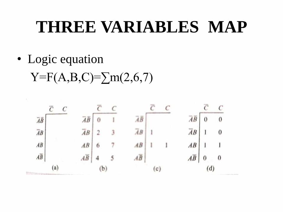
PAIRS AND QUADS AND OCTETS
• The map contain a pair of 1s that are
horizontally adjacent.(next to each other).
• The sum of product equation:
Y=ABCD+ABCD̅
which factor into
Y=ABC(D+D̅)

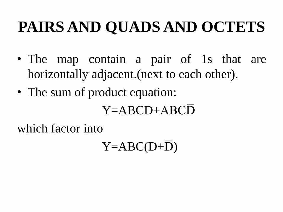
QUAD
• It is a group of four 1s that are horizontally orvertically adjacent.
• This is may be end to end.
• The Boolean equations of those two pairs:
Y=ABC̅ + ABC
Factor into
Y= AB(C̅ + C)
Which is reduce into
Y=AB


OCTET
• Besides pairs and quads, there is one more
group to adjacent 1s to look .
Y=AC̅ + AC
After factoring
Y=A(C̅ + C)
Reduce to
Y=A

KARNAUGH
SIMPLIFICATION
• Encircle the octet first
• Quad second
• And pairs last
In this way the greatest simplification results.
EQUATION: Y=A̅B̅C+A C̅+CD̅
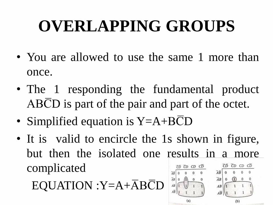
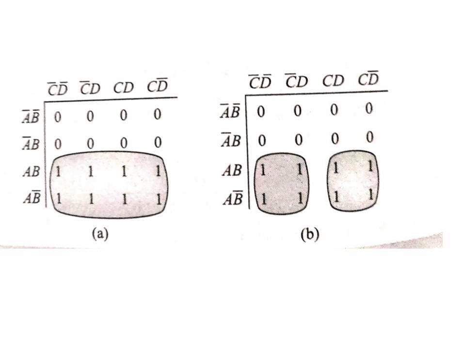
OVERLAPPING GROUPS
• You are allowed to use the same 1 more than
once.
• The 1 responding the fundamental product
ABC̅D is part of the pair and part of the octet.
• Simplified equation is Y=A+BC̅D
• It is valid to encircle the 1s shown in figure,
but then the isolated one results in a more
complicated
EQUATION :Y=A+A̅BC̅D
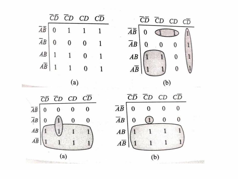

ROLLING THE MAP
• The pair result in this equation:
Y=BC̅D̅+BCD̅
Visualize Picking up the karnaugh map and rolling it so
that the left side touches the right side. if you are
visualizing correctly,you will realize the pairs actually
from a quad.to indicate this draw half circles around
each pair shown in fig., from this visualpoint the quad
has the equation:Y=BD̅

DON’T CARE CONDITIONS
• In some digital systems, certain never occur
during normal operations therefore, the
corresponding output never appear. since the
output never appears.it is indicated by an X in
the truth table

• Shows a truth table where the output is low for all the
entries from 0000 to 1000
• The high for input entry 1001 and X for 1010 through
1111
• The X is called a Don’t care conditions.
• Whenever you can see an X in a truth table,you can let
it equal either 0 or 1.
• Shown In the truth table with 1010 to 1111 with don’t
care for all inputs.
• Those don’t care are like wild cards in poker because
you can let them stand for whatever u like.
• Shown in fig2. the most efficient way to encirlce the 1.
• Notice two crucial ideas.

First the 1 is included in a quad,the largest group you
can find if u visualize all X’s as 1’S.
Second, after the 1 has been encircled, all X’s outside
the quad are visualized as 0’S.
In this way the X are used to the best possible
advantage.
As already mentioned, you are free to do this because
don’t care correspond to input condition that never
appear.
The quad boolean equation =Y=AD

• Logical circuit:
• The show in logical circit is AND gate with
inputs of A and D.
• You can check this logic circuit by examining
truth tacble.
• The possible inputs are from 0000 to 1001 in
this range a high A and D produce a high Y
• In this range a high A and D produce high Y
only for input condition 1001

Conditions
• Given the Truth table draw a Karnaugh Map
with 0’S and1s and don’t cares.
• Encircle the actual 1s on the Karnaugh map in
the largest groups you can find by treating the
don’t cares as 1s.
• After the actual 1s have been included in
groups, disregarded the remaining don’t cares
by visualizing them as 0s.

Product of sums method
• With the sum of product s method the design starts
with a truth table that summarizes the desired input –
output conditions.
• Next step to convert the truth table into an equivalent
sum of product equations.
• Final step is to draw the AND –OR network or its
NAND-NAND equivalent.
• The product of sums method is similar .
• Given a truth table u identify the fundamental sums
needed for a logical design.
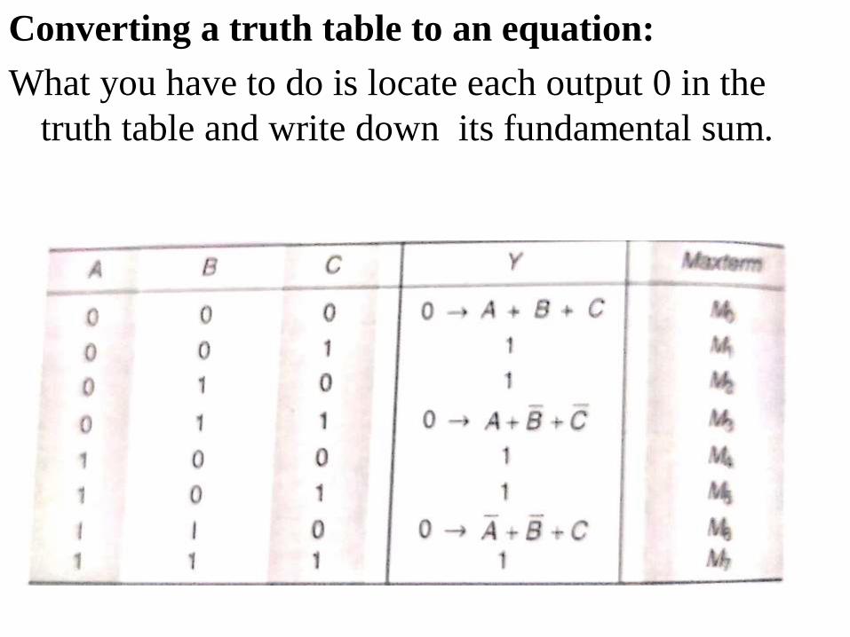
Converting a truth table to an equation:
What you have to do is locate each output 0 in the
truth table and write down its fundamental sum.

Logical circuit:
• After you have s product of sum equation you can get
the logical circuit by drawing an OR-AND network. or
if you prefer NOR-NOR network.
• Each sum represent the output of a 3 inputs OR gate
• The logical product of y is the output of a 3input AND
gate.
A 3 input OR gate is not available as a TTL chip. shown in
below fig.,is not practical with De Morgan’s first
theorem.
However you can replace the OR-AND circuit
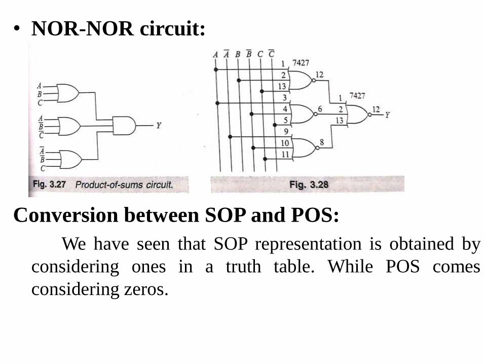
• NOR-NOR circuit:
Conversion between SOP and POS:
We have seen that SOP representation is obtained by
considering ones in a truth table. While POS comes
considering zeros.
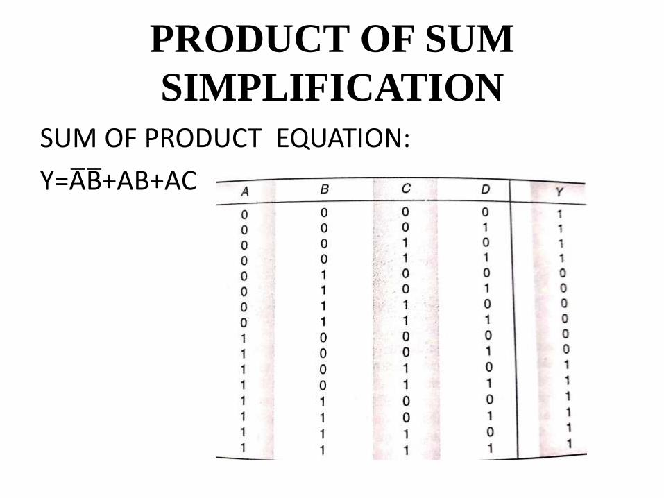
PRODUCT OF SUM
SIMPLIFICATION
SUM OF PRODUCT EQUATION:
Y=A̅B̅+AB+AC


DATA PROCESSING CIRCUITS
MULTIPLEXER:
Multiplexer mean many into one.
A multiplexer is a circuit with many inputs but only one output.

16 to 1 multiplexer:
The input bits are labeled D0 to D15,only one of
those is transmitted to the output. Which depends on
the value of ABCD, the control input.


DEMULTIPLEXER
• Demultiplexer means one to many
• A demultiplexer is a logic circuit with one input and
many output
.
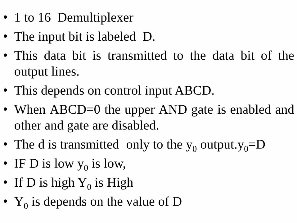
• 1 to 16 Demultiplexer
• The input bit is labeled D.
• This data bit is transmitted to the data bit of the
output lines.
• This depends on control input ABCD.
• When ABCD=0 the upper AND gate is enabled and
other and gate are disabled.
• The d is transmitted only to the y0 output.y0=D
• IF D is low y0 is low,
• If D is high Y0 is High
• Y0 is depends on the value of D
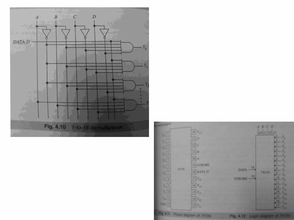

• 1 to 16 DECODER
a decoder is similar to a demultiplexer.
With only one exception there is no data input.
The only inpputs are the control bit ABCD.
The 74154 is the decoder de multiplexer.
The ABCD possibilities 0000 to 1111 ,you will find
that the subscript of the high output always equal the
decimal equivalent. that is called binary to decimal
decoder.

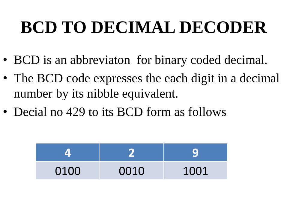
BCD TO DECIMAL DECODER
• BCD is an abbreviaton for binary coded decimal.
• The BCD code expresses the each digit in a decimal
number by its nibble equivalent.
• Decial no 429 to its BCD form as follows
4 2 9
0100 0010 1001

• Bcd to Decimal Decoder:
the above shown figure is called 1 to 10 decoder.
because only 1 of these 10 output lines is high for
instance, when ABCD is 0011,only theY3 AND gate
has all High inputs.
Therefore only y3 output is high.
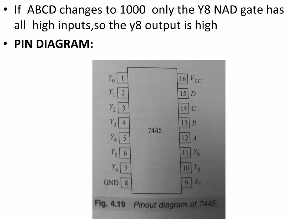
• If ABCD changes to 1000 only the Y8 NAD gate has all high inputs,so the y8 output is high
• PIN DIAGRAM:
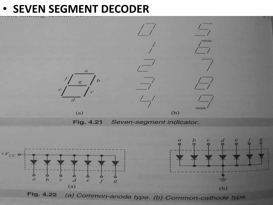
• SEVEN SEGMENT DECODER

ENCODER
• AN encoder converts an active input signal into a
coded output signals.
• The n input lines, only one of which is active.
• Internal logic with in the encoder converts this
active input to a coded binary output with m bits.
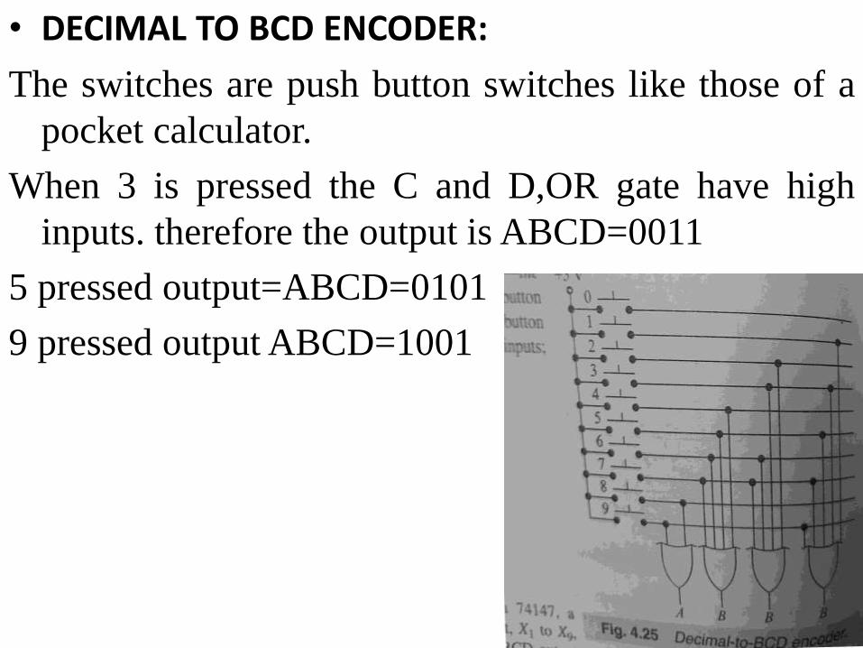
• DECIMAL TO BCD ENCODER:
The switches are push button switches like those of a
pocket calculator.
When 3 is pressed the C and D,OR gate have high
inputs. therefore the output is ABCD=0011
5 pressed output=ABCD=0101
9 pressed output ABCD=1001

• Pin out diagram:
the 74147 is a Decimal to BCD Encoder
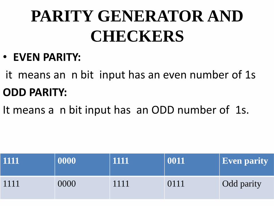
PARITY GENERATOR AND
CHECKERS
• EVEN PARITY:
it means an n bit input has an even number of 1s
ODD PARITY:
It means a n bit input has an ODD number of 1s.
1111 0000 1111 0011 Even parity
1111 0000 1111 0111 Odd parity
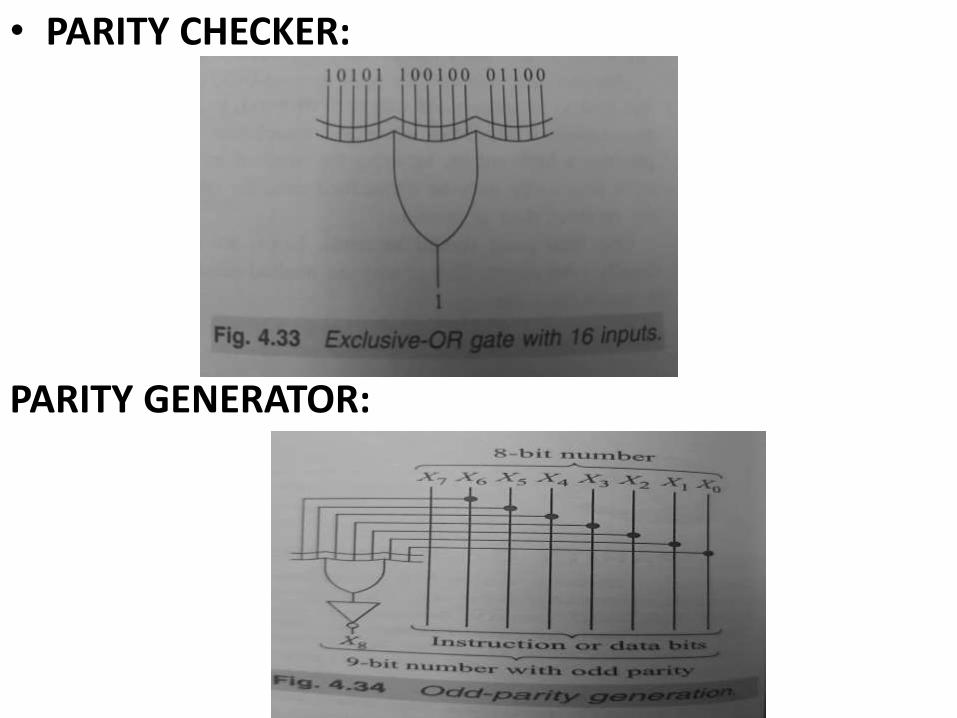
• PARITY CHECKER:
PARITY GENERATOR:
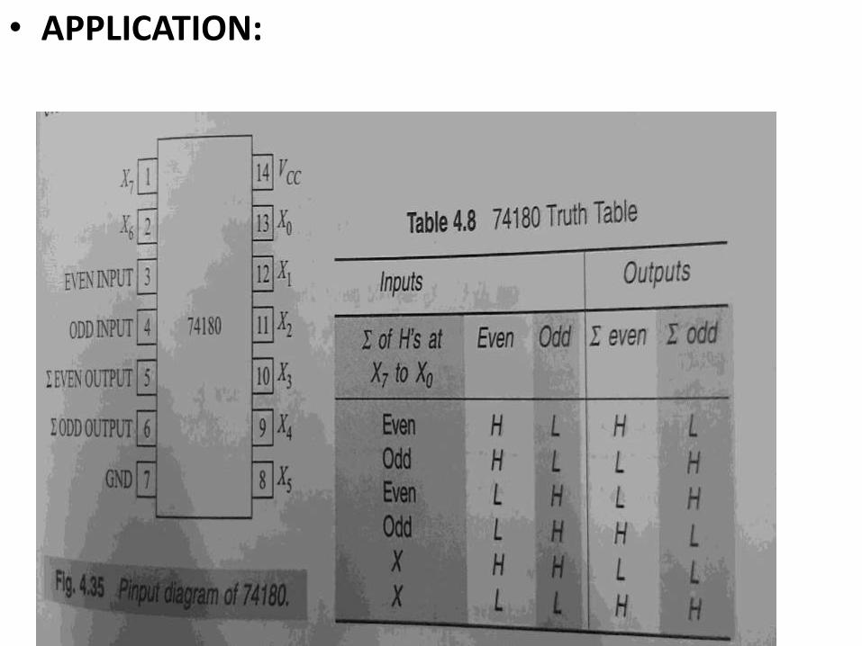
• APPLICATION:
BINARY NUMBER SYSTEM
1. It is a system that uses only the digit 0 and 1
as code.
2. All the other digits thrown away(0 to 9).
3. To represent decimal numbers and letters of
the alphabet with the binary code.
4. Where string of dots and dashes are used to
code all numbers and letters.

DECIMAL ODOMETER:
to understand how to count with binary numbers.
it help to review how an odometer counts with decimal
numbers.(miles indicator of a car or bike).
when a new car odometer start 00000
after 1 km 00001 and so on
At the end of the 9th km the number may be changed to
00010.
RESET AND CARRY
The unit wheels has reset to 0 and sent carry to the tens
wheel.
The other wheels of an odometer also reset carry.
For instance after 999 km the odometer shows
00999
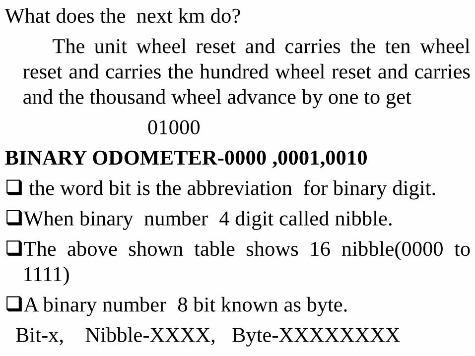
What does the next km do?
The unit wheel reset and carries the ten wheel
reset and carries the hundred wheel reset and carries
and the thousand wheel advance by one to get
01000
BINARY ODOMETER-0000 ,0001,0010
the word bit is the abbreviation for binary digit.
When binary number 4 digit called nibble.
The above shown table shows 16 nibble(0000 to
1111)
A binary number 8 bit known as byte.
Bit-x, Nibble-XXXX, Byte-XXXXXXXX


BINARY TO DECIMAL CONVESION:
• The list of binary numbers from 0000 to 1111.
• This session shows how to convert the binary no
quickly and easily into this decimal equivalent.
Positional notation and weights:
we can express any decimal integer(whole number) in
units, tens, hundred, thousand, and so on.
Decimal number 2945 may be written as
2000+900+40+5
in power of 10 becomes
2945=2(103)+9(102)+4(101) +5(100)
Decimal number is an example of positional notation
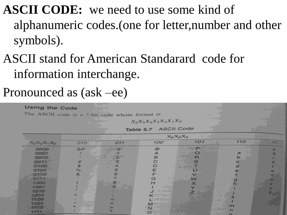
ASCII CODE: we need to use some kind of
alphanumeric codes.(one for letter,number and other
symbols).
ASCII stand for American Standarard code for
information interchange.
Pronounced as (ask –ee)

Parity bit:
The ASCII code is used for sending digital data over telephone line.as mentioned in the preceding 1 bit error may occur in transmitted data.
A parity bit is usually transmitted along with the original bits.
The parity checker at the receiving end can test for even or odd parity.
The ASCII code uses the 7 bits, the addition of bits is format is parity bit.
X7X6X5X4 X3X2X1X0
X7 IS PARITY BIT
this is an illegal length of digital equaling

EXCESS -3 CODE
the excess 3 code is an important 4 bit code used with
binary coded decimal number.
To convert an any decimal number into its excess-3 form
,add 3 to each decimal digit and then convert the sum
to BCD number.
For example :12
1+3=4 2+3=5
40100 5 0101
So 0100,0101 in the excess 3 code stands for decimal 12

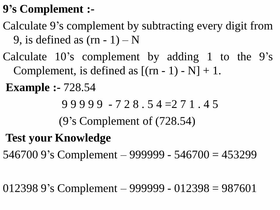
9’s Complement :-
Calculate 9’s complement by subtracting every digit from
9, is defined as (rn - 1) – N
Calculate 10’s complement by adding 1 to the 9’s
Complement, is defined as [(rn - 1) - N] + 1.
Example :- 728.54
9 9 9 9 9 - 7 2 8 . 5 4 =2 7 1 . 4 5
(9’s Complement of (728.54)
Test your Knowledge
546700 9’s Complement – 999999 - 546700 = 453299
012398 9’s Complement – 999999 - 012398 = 987601

GRAY CODE:
A Gray Code represents numbers using a binary encoding
scheme that groups a sequence of bits so that only one
bit in the group changes from the number before and
after.
It is named for Bell Labs researcher Frank Gray, who
described it in his 1947 patent submittal on Pulse Code
Communication. He did not call it a Gray Code, but
noted there was no name associated with the novel code
and referred to it as a Binary Reflected Code for the
way he determined the groupings and number
representations. When the patent was granted in 1953
others began to refer to the encoding scheme as the
Gray Code.

BCD code is some time referred as 8421 code
Decimal (base 10) Binary (base 2) Binary-Reflected (no base)
0 0000 0000
1 0001 0001
2 0101 0011
3 0011 0010
4 0100 0110
5 0101 0111
6 0110 0101
7 0111 0100
8 1000 1100
9 1001 1101
10 1010 1111

From this table we can obtain the
equivalent gray code of the decimal numbers. There
are several steps which will make you understand
how the codes are formed. (1) In case of gray code
one bit will change from its previous in each steps.
One thing must be kept in mind that the change of
bit always occurs from the right side i.e from L.S.B
towards the M.S.B. At first the first three bits are
constant I,e 000 and the fourth bit changes from 0 to
1. We know that for binary digit possible
combination is 0 and 1, so keeping first three bit
constant the possible combination of 4th bit is over
for decimal 0 and 1 respectively.
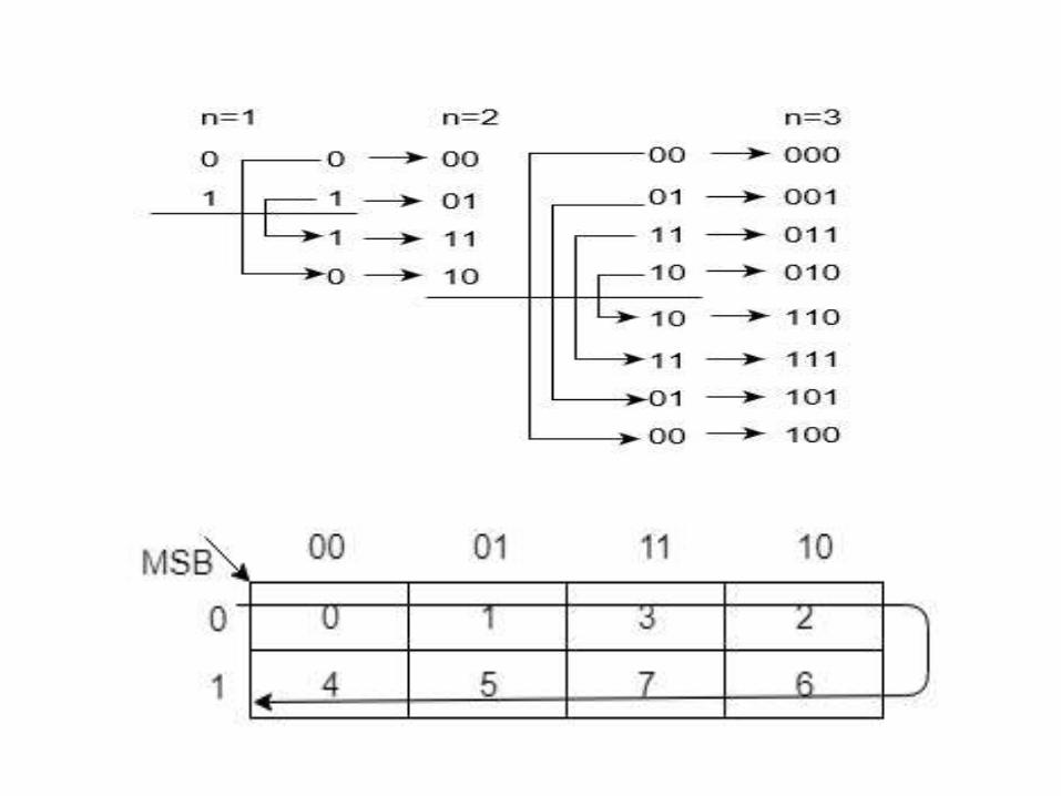

For n = 1 bit For n = 2 bit For n = 3bit
Binary Gray Binary Gray Binary Gray
0 0 00 00 000 000
1 1 01 01 001 001
10 11 010 011
11 10 011 010
100 110
101 111
110 101
111 100

ARITHMATIC CIRCUITS
Circuits that can perform binary addition and
subtraction are constructed by combining logic
gates.
These circuits are used in the design of the Arithmetic
and logic unit(ALU).
Binary Addition:
numbers represent physical quantities.
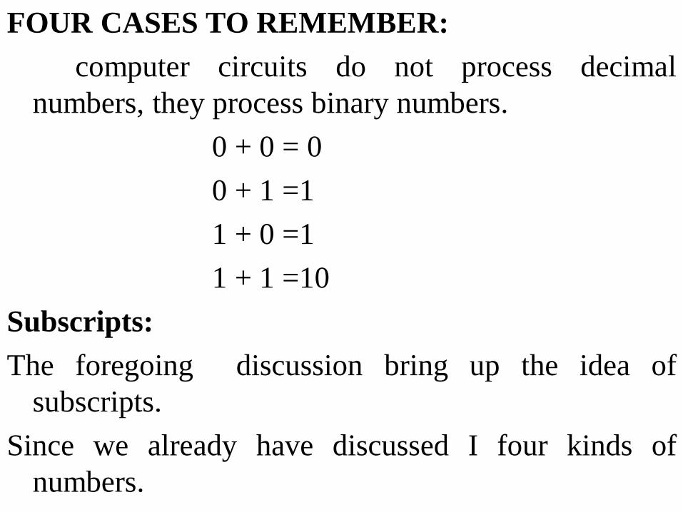
FOUR CASES TO REMEMBER:
computer circuits do not process decimal
numbers, they process binary numbers.
0 + 0 = 0
0 + 1 =1
1 + 0 =1
1 + 1 =10
Subscripts:
The foregoing discussion bring up the idea of
subscripts.
Since we already have discussed I four kinds of
numbers.

Decimal,Binary,Octal,and HExaDecimal.
2 -> Binary
8-> octal
10 -> decimal
16-> HexaDecimal
112 represent Binary
238 stands for octal
4510 for decimal
F416 for Hexadecimal

Larger Binary numbers:
11100 + 11010=110110
BINARY SUBTRACTION:
Let us begin with 4 basic cases of binary sbtraction
0-0=0
1-0=1
1-1=0
10-1=1
Larger numbers:
1101-1010=0011
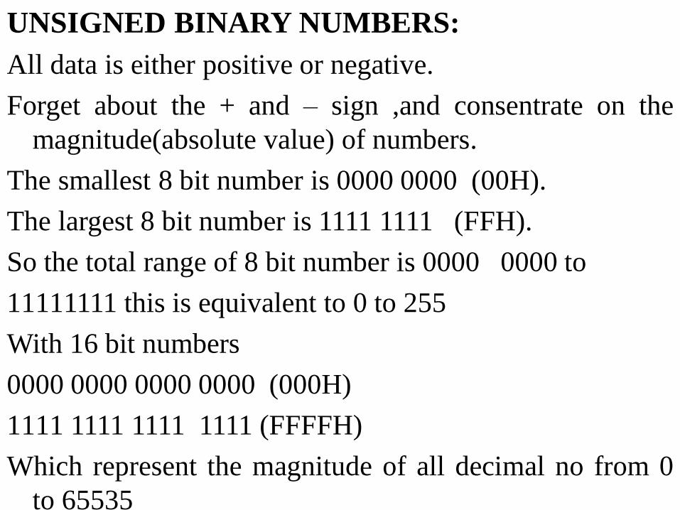
UNSIGNED BINARY NUMBERS:
All data is either positive or negative.
Forget about the + and – sign ,and consentrate on the
magnitude(absolute value) of numbers.
The smallest 8 bit number is 0000 0000 (00H).
The largest 8 bit number is 1111 1111 (FFH).
So the total range of 8 bit number is 0000 0000 to
11111111 this is equivalent to 0 to 255
With 16 bit numbers
0000 0000 0000 0000 (000H)
1111 1111 1111 1111 (FFFFH)
Which represent the magnitude of all decimal no from 0
to 65535

LIMITS:
1ST GENERATIO OF computer can process
only 8 bit at a time.
Therefore each number being added or
subtracted must be between 0 to 255.
If any magnitude are greater than 255,you
should use 16 bit arithmetic
Which means lower 8 bit first
Higher 8 bit is next.
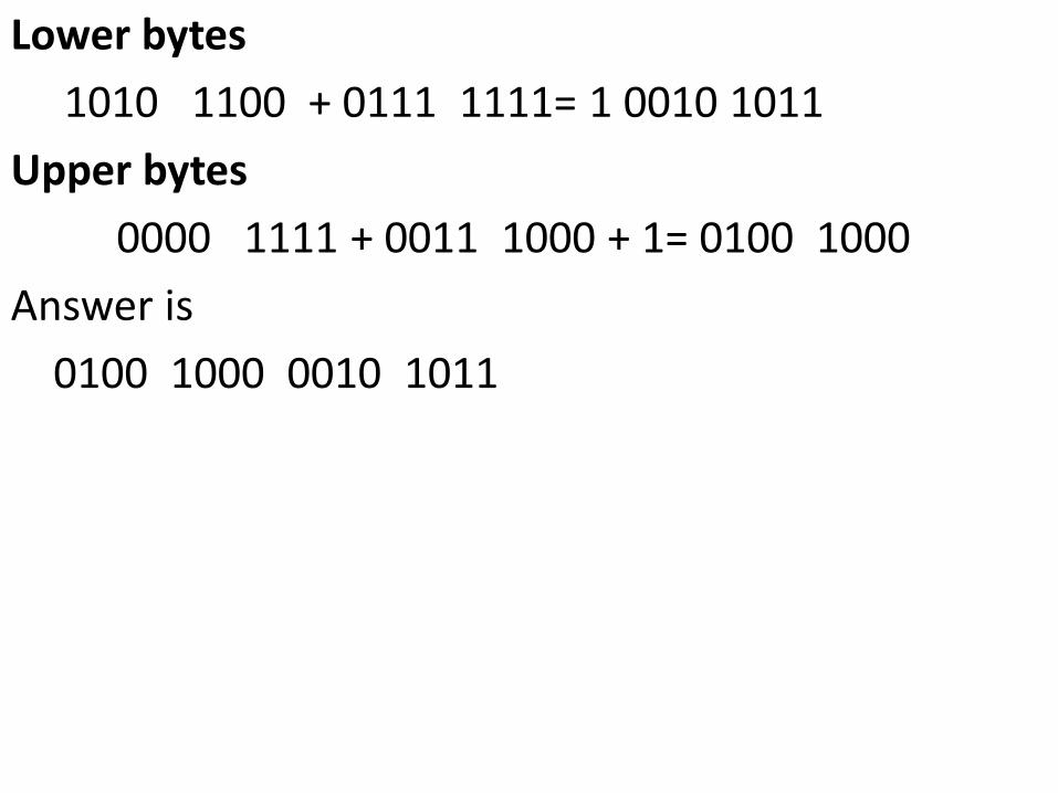
Lower bytes
1010 1100 + 0111 1111= 1 0010 1011
Upper bytes
0000 1111 + 0011 1000 + 1= 0100 1000
Answer is
0100 1000 0010 1011

Overflow:
In 8 bit arithmetic, addition of two
unsigned numbers whose sum is greater than 255
causes an overflow. A carry into the ninth column.
Most microprocessor have a logic circuit called a
carry flag. this circuits detects a carry into the ninth
column and warm you that the 8 bit answer is
invalid.
Example:175+118=293 answer is greater 255
175= AFH=1010 1111
118=76H=0111 0110
10101 1111 + 0111 0110 =1 0010 0101
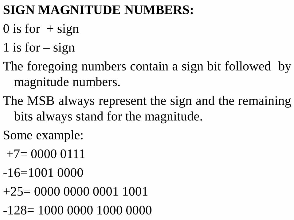
SIGN MAGNITUDE NUMBERS:
0 is for + sign
1 is for – sign
The foregoing numbers contain a sign bit followed by
magnitude numbers.
The MSB always represent the sign and the remaining
bits always stand for the magnitude.
Some example:
+7= 0000 0111
-16=1001 0000
+25= 0000 0000 0001 1001
-128= 1000 0000 1000 0000

2’s complement representation:
There is a rather unusual number system that
leads to the simple logic circuits for performing arithmetic
known as 2’s complement representation.
1’s complement:
1010=0101
1110 1100=0001 0011
0011 1111 0000 0110 = 1100 0000 1111 1001
2’s complement:
2’s complement= 1’s complement + 1
Example:
1011=0100(1’s complement)
0100 +1=0101( 2’s complement)
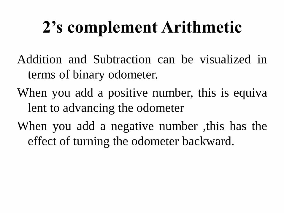
2’s complement Arithmetic
Addition and Subtraction can be visualized in
terms of binary odometer.
When you add a positive number, this is equiva
lent to advancing the odometer
When you add a negative number ,this has the
effect of turning the odometer backward.
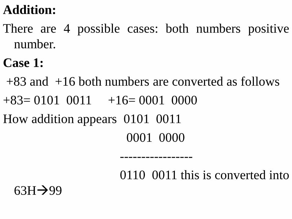
Addition:
There are 4 possible cases: both numbers positive
number.
Case 1:
+83 and +16 both numbers are converted as follows
+83= 0101 0011 +16= 0001 0000
How addition appears 0101 0011
0001 0000
-----------------
0110 0011 this is converted into
63H99

Case 2:
Positive and smaller negative.
+125 and -68
+1250111 1101
-68 1011 1100
---------------------------
571 0011 100139H57
Case 3:
Small positive larger negative
+37 and -115 =-78
0010 0101
1000 1101
---------------
1011 0010=B2H78
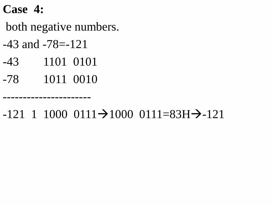
Case 4:
both negative numbers.
-43 and -78=-121
-43 1101 0101
-78 1011 0010
----------------------
-121 1 1000 01111000 0111=83H-121

Subtraction:
There are 4 possible chance to work .
Case 1:
both number is positive.
Case 2:
larger positive and negative no.
Case 3: positive and larger negative no.
Case 4: both negative no.-43 and -78 -43 1101 0101 -781011 0010
-781011 0010 2’s complement is 0100 1110
-431101 0101
+780100 1110
---------------------------
35 1 0010 0011
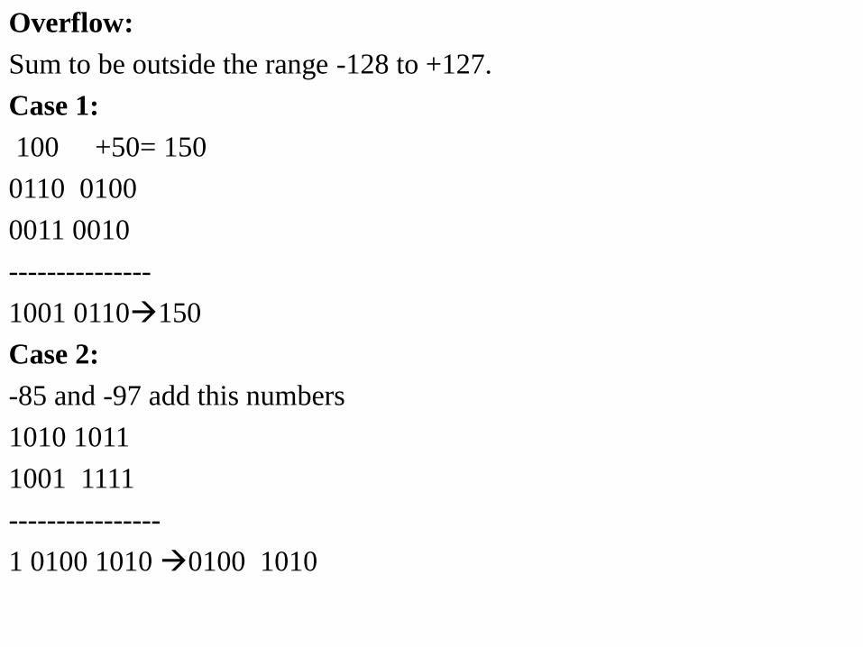
Overflow:
Sum to be outside the range -128 to +127.
Case 1:
100 +50= 150
0110 0100
0011 0010
---------------
1001 0110150
Case 2:
-85 and -97 add this numbers
1010 1011
1001 1111
----------------
1 0100 1010 0100 1010

ARITHMATIC BUILDING BLOCKS:
A logic circuit that performs 8 bit
arithmetic on positive and negative numbers.
First we need to cover three basic circuits
that will be used as building blocks.
These building blocks are Half adder ,Full
adder and Controlled Inverter.
Only these work it is only a short step to
step come together. that is how computer is able to
add and subtract binary numbers at any length.

Half Adder:
when we add two binary numbers we start with
the least significant column. This means that we
have to add two bits with the possibility of carry. the
circuit used for this is called half adder.
The output of the ex-or gate is called the SUM.
Output of the AND gate is Carry.
The AND gate produces high output only. when the
both inputs are high the Ex-OR output is high

Full Adder:
We have to use a full adder, a logic circuit
that can be add 3 bit at a time that is caller full
adder.
ABC input arte high this agrees with carry
the output is high. the odd number of high inputs
the Ex-OR gate output is high .

Controlled inverter:
It transmits the 8 bit input to the output.
When invert is low it transmit the 8bit input to the
output.
When invert is high it transmit the 1’s complement .
For example:
a low invert y7 …. Y0 = 0110 1110
But a high invert result in y7 …. Y0 = 1001 0001.
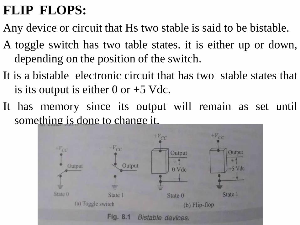
FLIP FLOPS:
Any device or circuit that Hs two stable is said to be bistable.
A toggle switch has two table states. it is either up or down,
depending on the position of the switch.
It is a bistable electronic circuit that has two stable states that
is its output is either 0 or +5 Vdc.
It has memory since its output will remain as set until
something is done to change it.
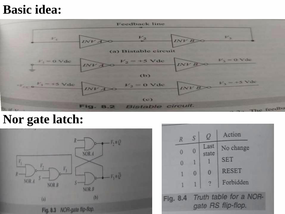
Basic idea:
Nor gate latch:
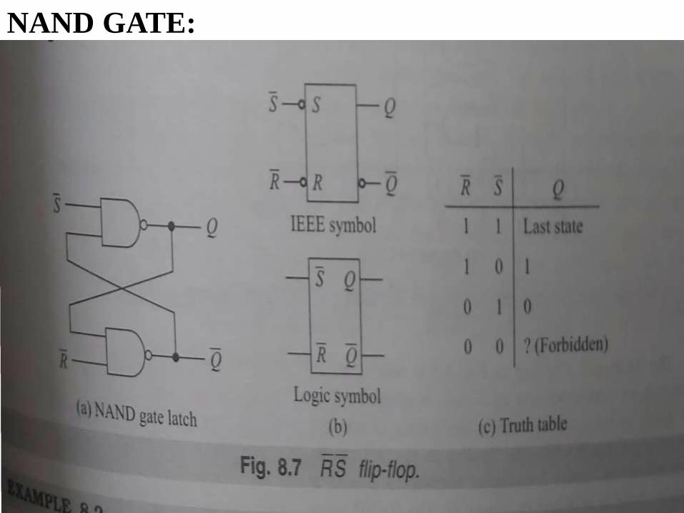
NAND GATE:

EDGE TRIGGERED RS FLIPFLOPS:
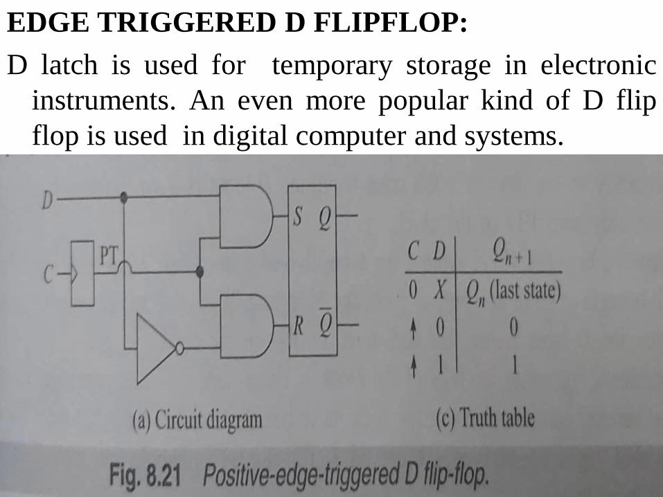
EDGE TRIGGERED D FLIPFLOP:
D latch is used for temporary storage in electronic
instruments. An even more popular kind of D flip
flop is used in digital computer and systems.

Edge triggered JK flip flop:
This is versatile circuit.
Counters can be used to count the number of PTs and
NTs of clock.

JK MASTER SLAVE FLIP FLOP:
master is positive edge triggerd
Salve is negative edge triggered.
REGISTERS:
• A register is a very important building blocks.
• Store a binary information appearing at an output of
an encoding matrix.
• Register must be accept the input an alphanumeric
keyboard.
• Then present in this data at the input of the
microprocessor.
• The asynchronous receiver transmitter(UART)is
chio used to exchange the data in a microprocessor
system.
• UART is constructed a register some control logic.
TYPES OF REGISTERS:
A register simply a group of flip flop that can be used to
store a binary number.
A register to store a 8 bit binary numbers must have the 8
flip flops.
Binary number can be entered(shifted) in to the register
and possibly shifted out.
A group of flip flop connected to provide either or both of
those function is called shift register.
The bits of the binary number moves from one place to
another in either of two ways .

Methods of shift:
1. The first method of shifting the data 1bit at a time in a serial
fashion beginning with either MSB or LSB. this technique is
called serial shifting.
2. The second method involves shifting all the data bits
simultaneously and is referred to as parallel shifting.
There are two ways to shift a data into a register
Serial and parallel.
Types :
1. Serial in serial out-8 bits
2. Serial in parallel out- 8 bits
3. Parallel in serial out- 8 bit
4. Parallel in parallel out- 4 bits
5. Parallel in parallel out-8 bits


SERIAL IN SERIAL OUT:


SERIAL IN PARALLEL OUT:

PARALLEL IN SERIAL OUT:

PARALLEL IN PARALLE OUT:

MEMORY:
Semiconductor memory
1.Bipolar transistor
2.MOS transistor(IC)
Real memory
1.ROM
2.RAM
Large amount of data are generally stored using
magnetic memory techniques.
Magnetic memory includes recording of digital
information on magnetic tape,HDD,FD.

SEMICONDUCTOR MEMORY:
• It consist of rectangular array of memory cells.
• Fabricated on silicon wafer.
• Stored and charge the 1 bit information.
• Memories are classified as bipolar or metal
oxide semiconductor.
• Complementary MOS-used to construct the
individual memory cells.
• It is greater packing and reduced size and cost.
• Lower power requirements.
Characteristics:
Two categories of memory RAM and ROM
RAM
1. SRAM
Smaller and rapid access type of cached memory.
2.DRAM
Bulk of memory and high speed.
PROM-data stored in Permanently.
EPROM- Erased programmed read only only.
Control:
Chip selected
Chip enable
ROM :
NONvolatile data storage.
MAGNETIC MEMORY:
Magnetic tape is produced by deposition of a
film of magnetic material on a large strip of plastic,
which is then wound on reel.

Magnetic recording:
Magnetic tape:
HDD
FD
OPTICAL MEMORY:
CD ROM
CD R
CDRW
DVD