Fundamentals on Electronics: A Design Oriented Teaching ...
81
0 1 st African Webinar Series on Fundamentals on Circuits, Systems, and Emerging Technologies 1 st African Webinar Series on Fundamentals on Circuits, Systems, and Emerging Technologies Jose Silva-Martinez Department of Electrical and Computer Engineering Texas A&M University Fundamentals on Electronics: A Design Oriented Teaching Methodology
Transcript of Fundamentals on Electronics: A Design Oriented Teaching ...

01st African Webinar Series on Fundamentals on Circuits, Systems, and Emerging Technologies
1st African Webinar Series on Fundamentals on Circuits, Systems, and Emerging Technologies
Jose Silva-Martinez
Department of Electrical and
Computer Engineering
Texas A&M University
Fundamentals on Electronics: A Design
Oriented Teaching Methodology
11st African Webinar Series on Fundamentals on Circuits, Systems, and Emerging Technologies
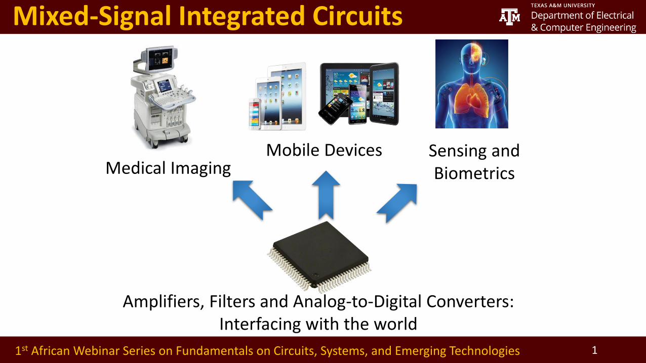
Mixed-Signal Integrated Circuits
Mobile DevicesMedical Imaging
Sensing and Biometrics
Amplifiers, Filters and Analog-to-Digital Converters: Interfacing with the world

21st African Webinar Series on Fundamentals on Circuits, Systems, and Emerging Technologies
Market Growth in Wireless Communications
Smartphones By 2016 market > 2B units*
*Business Insider: The global smartphone market report

31st African Webinar Series on Fundamentals on Circuits, Systems, and Emerging Technologies
Important Features: Wireless; 5G and Beyond
f
Carrieragregation
GHz
singlecarrier
High bandwidth (160 MHz)
• Carrier aggregation
• Full band capture
High resolution (>10 bit)
• Presence of blockers requires high dynamic range
• Better Linearity (Co-existence)
Low power consumption
• Extent battery life of wireless receivers.

41st African Webinar Series on Fundamentals on Circuits, Systems, and Emerging Technologies
There are multiple architectures to select, depending on your bandwidth and resolution requirements.
4
6
8
10
12
14
0.1 1 10 100 1000
EN
OB
(b
its
)
BW (MHz)
ΣΔ
Pipeline
SAR
Flash,
t.i. SAR
Sigma delta (ΣΔ) and pipeline ADCs are the bestarchitectures for broadband wireless receivers
6 8 10 12 14 16 18
0.0
1 0
.1 1
1
0
Cable TV
Spectrum
Analizers
Ultrasound
Radar
Automotive
Wireless
InfrastructureFlat Panel
Defense
Communications
RadarSonet
Digital
Oscilloscope
Emerging
802.11ax
Effective number of bits
Sig
na
l B
an
dw
idth
(G
Hz)
Mixed-Signal Integrated Circuits

51st African Webinar Series on Fundamentals on Circuits, Systems, and Emerging Technologies
Technology Trend: Increased throughput
Low-Noise and Linear Amplifiers
High Performance Filters
High performance Up/Down Converters
High-performance Frequency Synthesizers
High performance A/D and D/A
But technology trend is towards faster and smaller
transistors but limited performance for Analog Functions:
Back to fundamentals: Linear feedback (Calibration) is a
suitable option

61st African Webinar Series on Fundamentals on Circuits, Systems, and Emerging Technologies
How to prepare for these challenges?
• Teaching electronics:
• Millman-Halkias: One of the most popular books in the 70’s and early 80’s.
• Nicely written and large number of examples. 75% Analog and 25% Digital
• Sedra-Smith: Replaced Millman-Halkias. The most popular textbook on electronics during the last 20 years. Many authors follow this style. Less algebra and more insight. >1800 pages, 50% Analog and 50% digital electronics.

71st African Webinar Series on Fundamentals on Circuits, Systems, and Emerging Technologies
Teaching Electronics:
• Ravazi: Recent book, becoming very popular. Updated material. Nice book with videos available through youtube.
• A large number of excellent textbooks are available, but students have to digest the material in 14-15 weeks.

81st African Webinar Series on Fundamentals on Circuits, Systems, and Emerging Technologies
Challenges in today’s education
Big books with plenty of derivations help with the analysis of circuits, but make
difficult for students to digest properly the concepts;
Too compact, we endup with a cook book; hard to understand the most relevant
concepts;
Analysis with the aim of obtaining DC and AC equations do not necessarily help
students to understand the fundamentals;
Major device limitations should be emphasized as well;
Design approach: Students must be able to design working circuits, not just analysis;
Proper management of the simulators;
Hands on experience is essential to fully digest the material;

91st African Webinar Series on Fundamentals on Circuits, Systems, and Emerging Technologies
Outline
First part:Revising BJT FundamentalsSmall-signal Model for the BJT: A Linear Approximation.Transistor characterization and design approach.Design examples
CMOS Fundamentals (same topics as in BJTs)
10 minutes break

101st African Webinar Series on Fundamentals on Circuits, Systems, and Emerging Technologies
Outline
Second part:CMOS (Integrated circuits) blocks
Technology, modeling and noise
Current mirrors
Differential pair
OPAMPs
Advanced Amplifiers for ADCsPipeline ADCs
SD Modulators

111st African Webinar Series on Fundamentals on Circuits, Systems, and Emerging Technologies
Outline
Hands-On Experience Sessions: 2:30pm-4:45pm
Undergraduate examples: Please download LTSpice before the session; google LTSpice)Jose Silva-Martinez: Connecting theory with simulations
Tanwei Yan: Use of AD2 as oscilloscope, frequency synthesizer, network analyzer, vector analyzer
Advanced Mixed-Mode Systems: Pipeline ADC as an example Junning Jiang: Macromodels in Cadence (can also be built in LT Spice with
some limitations)
Amr Hassan: Transistor level realization of the first ADC stage, and simulations results and interpretations
121st African Webinar Series on Fundamentals on Circuits, Systems, and Emerging Technologies
Bipolar Junction Transistor Circuits

131st African Webinar Series on Fundamentals on Circuits, Systems, and Emerging Technologies
5.2 DC Characteristics of the BJT (Input)
• 𝑰𝑪 vs 𝑽𝑩𝑬 plot
𝑖𝐶 = 𝐼𝑆 𝑒𝑉𝐵𝐸𝑉𝑇𝐻 − 1
(in active region)
• Forward bias current
• 𝑉𝐵𝐸 = 0.7, for reasonable 𝐼𝐶
• Typical reverse saturation current 𝐼𝑆 < 0.1𝑝𝐴
IC (A)
VBE (V)0.6 0.8
QCQ
VBEQ
0.40.20.0-0.2-0.4
𝐼𝐶 vs 𝑉𝐵𝐸

141st African Webinar Series on Fundamentals on Circuits, Systems, and Emerging Technologies
5.2 DC Characteristics of the BJT (Output)
• 𝑰𝑪 vs 𝑽𝑪𝑬 plot
• 𝑉𝐵𝐸 is fixed for each sweep
• Two region of operation
• 𝑉𝐶𝐸 ≥ 300𝑚𝑉 → Active region
• 𝑉𝐶𝐸 < 300𝑚𝑉 → Saturation region
• Active region / Linear region
• 𝑖𝐶 = 𝐼𝑆 𝑒𝑉𝐵𝐸𝑉𝑇𝐻 − 1
• Saturation region
• 𝑖𝑐 = Depends on 𝑉𝐶𝐸 and 𝑉𝐵𝐸
C
VBE1
VCE
VBE4
VBE2
VBE3
VBE0
𝐼𝐶 vs 𝑉𝐶𝐸
• Cut-off region• 𝑉𝐵𝐸 < 0.5𝑉• 𝐼𝐶 , 𝐼𝐸 and 𝐼𝐵 are nearly zero
Saturation region
Active/Linear region

151st African Webinar Series on Fundamentals on Circuits, Systems, and Emerging Technologies
5.3 Small-signal Model for the BJT
RC
vbe
+
-
vCE
+
-
iC
How to analyze this circuit?
VBE
𝑉𝐵𝐸 + 𝑣𝑏𝑒 Q
VBE + vbe
ICQ + ic
Tim
e
Time
iC (A)
VBE (V)0.6 0.80.40.20.0
• Base-emitter voltage is mapped into collector-emitter current
• Larger 𝑉𝐵𝐸 implies larger 𝐼𝐶𝑄
• Larger input signal 𝑣𝑏𝑒 generates larger collector/emitter current
𝑖𝐶 = 𝐼𝑆 𝑒𝑉𝐵𝐸+𝑣𝑏𝑒
𝑉𝑡ℎ − 1 ≅ 𝐼𝑆𝑒𝑉𝐵𝐸𝑉𝑡ℎ 𝑒
𝑣𝑏𝑒𝑉𝑡ℎ = 𝐼𝐶𝑄 ⋅ 𝑒
𝑣𝑏𝑒𝑉𝑡ℎ
𝑖𝐶 = 𝐼𝐶𝑄 + 𝐼𝐶𝑄
𝑣𝑏𝑒
𝑉𝑡ℎ+
𝐼𝐶𝑄
2
𝑣𝑏𝑒
𝑉𝑡ℎ
2
+𝐼𝐶𝑄
6
𝑣𝑏𝑒
𝑉𝑡ℎ
3
+. . . .
161st African Webinar Series on Fundamentals on Circuits, Systems, and Emerging Technologies
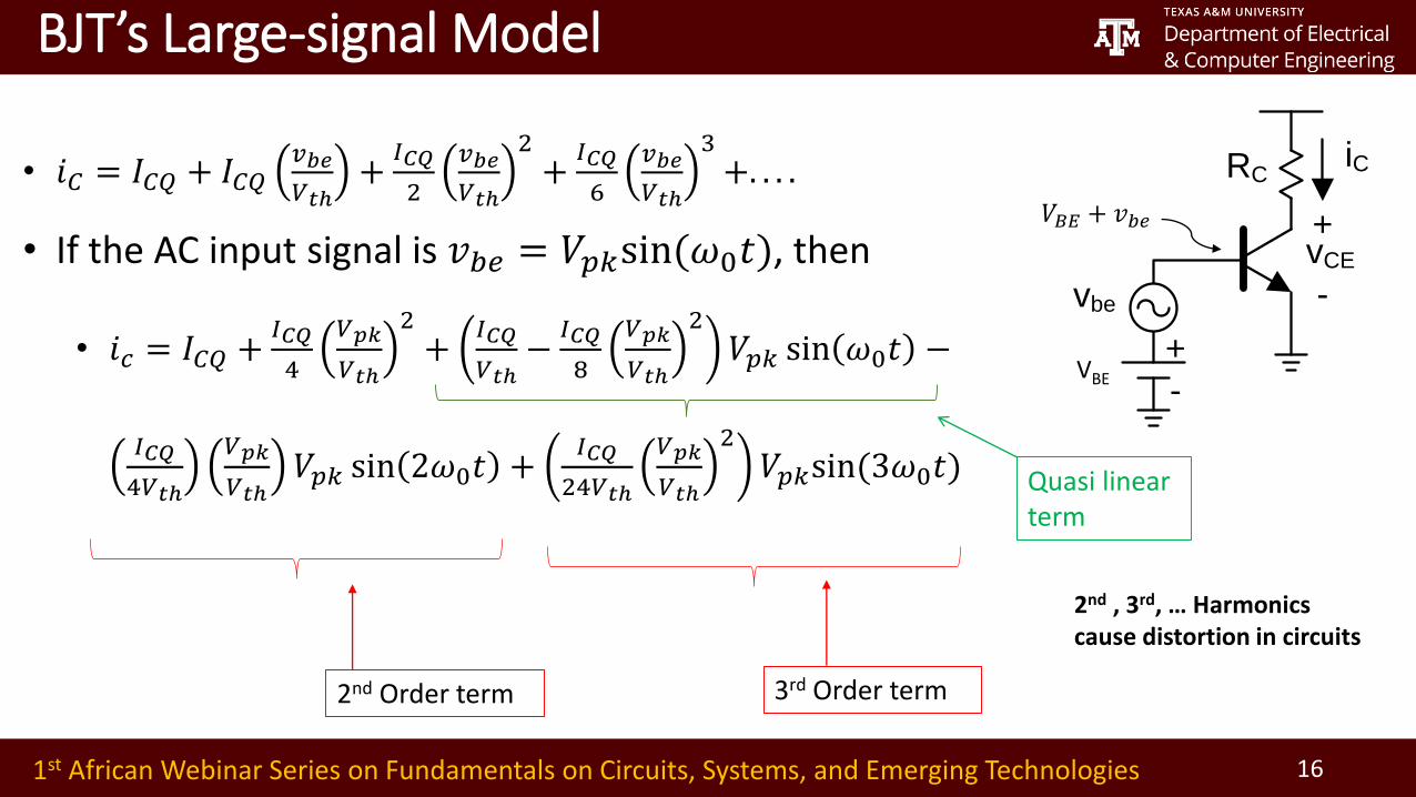
BJT’s Large-signal Model
VBE
RC
vbe
+
-
vCE
+
-
iC
𝑉𝐵𝐸 + 𝑣𝑏𝑒
• 𝑖𝐶 = 𝐼𝐶𝑄 + 𝐼𝐶𝑄𝑣𝑏𝑒
𝑉𝑡ℎ+
𝐼𝐶𝑄
2
𝑣𝑏𝑒
𝑉𝑡ℎ
2+
𝐼𝐶𝑄
6
𝑣𝑏𝑒
𝑉𝑡ℎ
3+. . . .
• If the AC input signal is 𝑣𝑏𝑒 = 𝑉𝑝𝑘sin(𝜔0𝑡), then
• 𝑖𝑐 = 𝐼𝐶𝑄 +𝐼𝐶𝑄
4
𝑉𝑝𝑘
𝑉𝑡ℎ
2+
𝐼𝐶𝑄
𝑉𝑡ℎ−
𝐼𝐶𝑄
8
𝑉𝑝𝑘
𝑉𝑡ℎ
2𝑉𝑝𝑘 sin 𝜔0𝑡 −
𝐼𝐶𝑄
4𝑉𝑡ℎ
𝑉𝑝𝑘
𝑉𝑡ℎ𝑉𝑝𝑘 sin 2𝜔0𝑡 +
𝐼𝐶𝑄
24𝑉𝑡ℎ
𝑉𝑝𝑘
𝑉𝑡ℎ
2𝑉𝑝𝑘sin(3𝜔0𝑡) Quasi linear
term
2nd Order term 3rd Order term
2nd , 3rd, … Harmonics cause distortion in circuits

171st African Webinar Series on Fundamentals on Circuits, Systems, and Emerging Technologies
5.3 Small-signal Model for the BJT
• If we assume 𝑉𝑝𝑘 < 0.4𝑉𝑡ℎ (small signal)
• 𝑖𝐶 = 𝐼𝐶𝑄 +𝐼𝐶𝑄
𝑉𝑡ℎ𝑣𝑏𝑒 ( Linear approximation)
• AC current linearly dependent on AC voltage
• Slope of 𝐼𝐶 vs 𝑉𝐵𝐸 is Transconductance
𝑔𝑚 = 𝜕𝑖𝐶
𝜕𝑣𝐵𝐸 𝑄=
𝐼𝐶𝑄
𝑉𝑡ℎ
This model does not capture amplifier’s non-linearities
Since the resulting circuit is linear, you can use any amplitude
Q
VBEQ
ICQ
iC (A)
VBE (V)0.6 0.80.40.20.0
QBE
Cm
v
ig

181st African Webinar Series on Fundamentals on Circuits, Systems, and Emerging Technologies
5.3 Small-signal Model for the BJT
• Modelling BJT
• 𝑖𝑐 is modelled as CCCS with 𝑔𝑚 =𝐼𝐶𝑄
𝑉𝑡ℎ
• Forward biased diode across Emitter and Collector
• Diode can be modelled as resistor 𝑟𝜋 and voltage source 0.7𝑉 series
• 𝑔𝜋 =1
𝑟𝜋=
𝜕𝑖𝐵
𝜕𝑣𝐵𝐸 𝑄=
𝐼𝐵𝑄
𝑉𝑡ℎ
E
IC+gmvbeiB
B
C
iE
iC
Q
VBEQ
ICQ
iC (A)
VBE (V)0.6 0.80.40.20.0
QBE
Cm
v
ig
E
IC+gmvbeiB
B
C
ie
ic
r
+
0.7V
-

191st African Webinar Series on Fundamentals on Circuits, Systems, and Emerging Technologies
5.4.4 𝝅 and T model for BJT
E
r
gmvbeib
C
rce
ie
ic
re
ie
ieib
C
rce
ic
𝜋 – hybrid model for BJT 𝑇 – model for BJT
• 𝑟𝑐𝑒 is the finite output resistance of BJT
• Choose model with makes solving circuit easier
• 𝑟𝑐𝑒 =𝐼𝐶𝑄
𝑉𝑒𝑎𝑟𝑙𝑦
• 𝑔𝜋 =1
𝑟𝜋=
𝜕𝑖𝐵
𝜕𝑣𝐵𝐸 𝑄=
𝐼𝐵𝑄
𝑉𝑡ℎ
• 𝑟𝑐𝑒 =𝐼𝐶𝑄
𝑉𝑒𝑎𝑟𝑙𝑦
• 𝑔𝑒 =1
𝑟𝑒=
𝜕𝑖𝐸
𝜕𝑣𝐵𝐸 𝑄=
𝐼𝐸𝑄
𝑉𝑡ℎ
Hence
𝑟𝑒 =𝑉𝑡ℎ
𝐼𝐸𝑄=
𝑉𝑡ℎ
1 + 𝛽 𝐼𝐵𝑄=
𝑟𝜋1 + 𝛽

201st African Webinar Series on Fundamentals on Circuits, Systems, and Emerging Technologies
5.4.1 DC analysis
• What is maximum tolerable value of 𝑣𝑏𝑒 ?
• BJT should be in active region always
• Lowest possible value of 𝑉𝐶 = 𝑉𝐵-0.4V
iC
VCE
Q
VCEQ
ICQ VBEQ
VCC
VCC/RC
0.3V
linear range
vbe-peak
vce-peak
RC
vbe
+
-
vCE
+
-
iC
VBE
𝑉𝐵𝐸 + 𝑣𝑏𝑒
Input signal swing
Output signal swing

211st African Webinar Series on Fundamentals on Circuits, Systems, and Emerging Technologies
5.4.5 Practical limitations
• 𝑉𝐶𝐸 > 300𝑚𝑉 needed to maintain linear mode of operation
• Non-ideal effects limit max. current density• Maximum achievable 𝛽 is limited
• Temperature sensitivity of parameters• 𝑟𝜋, 𝑔𝑚, and 𝛽 are sensitive to temperature
• Very large 𝑉𝐶𝐸 cause large 𝐼𝑐. • P-N junction breakdown
• Current gain (𝛽) reduces with frequency• poles due to internal resistance and capacitance
IC(mA)0.01
27º
0.1 1.0 10 100
250
200
150
110º
-50º
350
300
VCE
VBE1
VBE2
VBE3
VBE4
VBE5

221st African Webinar Series on Fundamentals on Circuits, Systems, and Emerging Technologies
5.5.1 Common emitter amplifier
VCC
RC
vbe
voiC
CC
RL
VBEQ+
- E
r
gmvbeib
B
RC
ie
C
vbe
vo
CC
RL
VCEQ
+
-
Small signal equivalent
Input Output
• AC solution
• Use KCL & KVL on above circuit
• 𝑣𝑜 = −𝑔𝑚𝑅𝐶𝑠𝑅𝐿𝐶𝐶
1+𝑠(𝑅𝐶+𝑅𝐿) 𝐶𝐶𝑣𝑏𝑒
• DC solution
• 𝐼𝐶𝑄 = 𝐼𝑆𝑒
𝑉𝐵𝐸𝑄
𝑉𝑡ℎ
• 𝑉𝐶𝐶 = 𝑉𝐶𝐸𝑄 + 𝐼𝐶𝑄𝑅𝐶

231st African Webinar Series on Fundamentals on Circuits, Systems, and Emerging Technologies
5.5.1 Common emitter amplifier
𝑣𝑜 = −𝑅𝐶𝑅𝐿
𝑅𝐶 + 𝑅𝐿𝑔𝑚𝑣𝑏𝑒 = −
𝑅𝐶𝑅𝐿
𝑅𝐶 + 𝑅𝐿𝑖𝑐
• Gain higher with static loading
• Gain reduction due to loading should be taken into account during design
iC
VCE
QICQ
VCC
VCC/RC
0.3V
static load
line (1/RC)
VCEQ
VBEQ
iC
VCE
QICQ
VCC
VCC/RC
0.3V VCEQ
static load
line (1/RC)dynamic load
line (1/[RC||RL])
VBEQ

241st African Webinar Series on Fundamentals on Circuits, Systems, and Emerging Technologies
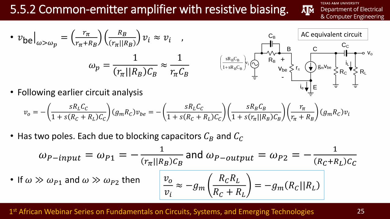
5.5.2 Common-emitter amplifier with resistive biasing.
• 𝑉𝐵𝐵 =𝑅𝐵
𝑅1𝑉𝐶𝐶 = 𝐼𝐵𝑄𝑅𝐵 + 0.7𝑉
• 𝑉𝐶𝐶 = 𝑉𝐶𝐸𝑄 + 𝐼𝐶𝑄𝑅𝐶
Here 𝐼𝐵𝑄 =𝐼𝐶𝑄
𝛽
Two equations, Four variables
𝑅1, 𝑅2, 𝑅𝑐 and 𝐼𝐶𝑄
VCC
RCICQ
RB
VB
+
-CC
B VR
R
1
+
-
VCEQ
IBQ
DC equivalent circuit• 𝑉𝐵𝐵 =
𝑅𝐵
𝑅1𝑉𝐶𝐶 = 𝐼𝐵𝑄𝑅𝐵 + 0.7𝑉
𝐼𝐵𝑄 =
𝑅𝐵𝑅1
𝑉𝐶𝐶 − 0.7
𝑅𝐵
𝐼𝐶𝑄 =
𝑅𝐵𝑅1
𝑉𝐶𝐶 − 0.7
𝛽 𝑅𝐵
• 𝐼𝐶𝑄 varies a lot, mainly due to 𝛽 variability.
251st African Webinar Series on Fundamentals on Circuits, Systems, and Emerging Technologies
5.5.2 Common-emitter amplifier with resistive biasing.
• 𝑣be 𝜔>𝜔𝑝=
𝑟𝜋
𝑟𝜋+𝑅𝐵
𝑅𝐵
𝑟𝜋||𝑅𝐵𝑣𝑖 ≈ 𝑣𝑖 ,
𝜔𝑝 =1
𝑟𝜋||𝑅𝐵 𝐶𝐵≈
1
𝑟𝜋𝐶𝐵
• Following earlier circuit analysis
• Has two poles. Each due to blocking capacitors 𝐶𝐵 and 𝐶𝐶
• If 𝜔 ≫ 𝜔𝑃1 and 𝜔 ≫ 𝜔𝑃2 then
RC
vo
RB +
vbe
-
CB
CC
RL
i
BB
BBv
CsR1
CsR
E
rgmvbe
ie
CB
iL
AC equivalent circuit
𝑣𝑜 = −𝑠𝑅𝐿𝐶𝐶
1 + 𝑠 𝑅𝐶 + 𝑅𝐿 𝐶𝐶𝑔𝑚𝑅𝐶 𝑣𝑏𝑒 = −
𝑠𝑅𝐿𝐶𝐶
1 + 𝑠 𝑅𝐶 + 𝑅𝐿 𝐶𝐶
𝑠𝑅𝐵𝐶𝐵
1 + 𝑠 𝑟𝜋||𝑅𝐵 𝐶𝐵
𝑟𝜋𝑟𝜋 + 𝑅𝐵
𝑔𝑚𝑅𝐶 𝑣𝑖
𝜔𝑃−𝑖𝑛𝑝𝑢𝑡 = 𝜔𝑃1 = −1
𝑟𝜋||𝑅𝐵 𝐶𝐵and 𝜔𝑃−𝑜𝑢𝑡𝑝𝑢𝑡 = 𝜔𝑃2 = −
1
𝑅𝐶+𝑅𝐿 𝐶𝐶
𝑣𝑜
𝑣𝑖≈ −𝑔𝑚
𝑅𝐶𝑅𝐿
𝑅𝐶 + 𝑅𝐿= −𝑔𝑚 𝑅𝐶||𝑅𝐿

261st African Webinar Series on Fundamentals on Circuits, Systems, and Emerging Technologies
5.6.1 Common-emitter amplifier
• Aim → Design Common Emitter amplifier with a high-frequency gain = 34 dB.
• Q2N222 BJT used for this design
• In general 𝛽𝐴𝐶 ≈ 200 and 𝛽𝐷𝐶 ≈ 200
• DC Transistor Characterization• Use this configuration to plot 𝑉𝐵𝐸 vs 𝐼𝑐• Use 𝑉𝐶𝐸 = 1𝑉, Since 𝑉𝐶𝐸 > 0.3𝑉 →
Linear region on

271st African Webinar Series on Fundamentals on Circuits, Systems, and Emerging Technologies
5.6.1 Common-emitter amplifierMeasure 𝐠𝐦
• 𝑔𝑚 =𝜕𝐼𝑐
𝜕𝑉𝐵𝐸
• Slope of curve
• Compare this value
with 𝑔𝑚 =𝐼𝐶𝑄
𝑉𝑡ℎ
• How to find out 𝑅𝐶?
Slope = gm @ IC=1.2mA
281st African Webinar Series on Fundamentals on Circuits, Systems, and Emerging Technologies
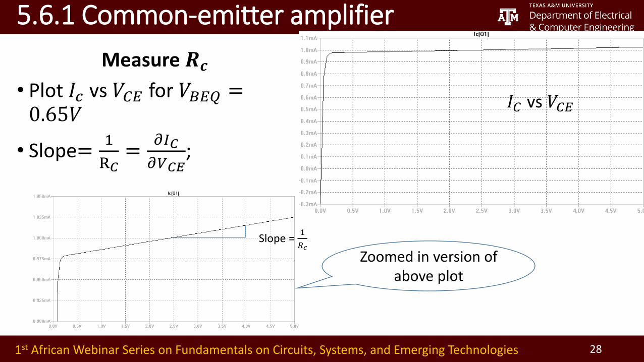
5.6.1 Common-emitter amplifier
Measure 𝑹𝒄
• Plot 𝐼𝑐 vs 𝑉𝐶𝐸 for 𝑉𝐵𝐸𝑄 =0.65𝑉
• Slope=1
R𝐶=
𝜕𝐼𝐶
𝜕𝑉𝐶𝐸;
Zoomed in version of above plot
𝐼𝐶 vs 𝑉𝐶𝐸
Slope = 1
𝑅𝑐

291st African Webinar Series on Fundamentals on Circuits, Systems, and Emerging Technologies
5.6.1 Common-emitter amplifier
Measure 𝒓𝝅
• Plot 𝐼𝐵 vs 𝑉𝐵𝐸at 𝑉𝐶𝐸 = 1𝑉
• Slope =1
𝑟𝜋= 𝑔𝜋
• 𝑔𝜋 =𝜕𝐼𝐵
𝜕𝑉𝐵𝐸Slope = g @ IB=5mA

301st African Webinar Series on Fundamentals on Circuits, Systems, and Emerging Technologies
Common emitter Circuit with source degeneration
• Previous design issue• Difficult to control operating point (𝐼𝑐)
• 𝑅𝐸1 and 𝑅𝐸2 are added at emitter
• 𝐶𝐸 to regain some of lost gain
• Advantages:• Circuit less sensitive to temperature• More control over 𝐼𝑐 and gain• Higher input impedance
•Drawbacks:• Reduced small signal gain
•
VCC
RC
vi
vC
RB1
RB2
vB
RE1
RE2 CE
CBRS
RL
vo
CL

311st African Webinar Series on Fundamentals on Circuits, Systems, and Emerging Technologies
DC analysis
𝑪𝑩 and 𝑪𝑳 are treated as open
𝑉𝐵𝐵 =𝑅𝐵
𝑅𝐵1𝑉𝐶𝐶 = 𝐼𝐵𝑄𝑅𝐵 + 0.7𝑉 + 𝐼𝐸𝑄 𝑅𝐸1 + 𝑅𝐸2
= 0.7𝑉 + 𝐼𝐶𝑄
𝑅𝐵
𝛽+
1
𝛼𝑅𝐸1 + 𝑅𝐸2
𝑅𝐵 = 𝑅𝐵1||𝑅𝐵2
𝑉𝐶𝐶 = 𝑉𝐶𝐸𝑄 + 𝐼𝐶𝑄𝑅𝐶 + 𝐼𝐸𝑄 𝑅𝐸1 + 𝑅𝐸2
= 𝑉𝐶𝐸𝑄 + 𝐼𝐶𝑄 𝑅𝐶 +𝑅𝐸1 + 𝑅𝐸2
𝛼
VCC
RC
vi
vC
RB1
RB2
vB
RE1
RE2 CE
CBRS
RL
vo
CL
VCC
RCRB1
RB2
vB
RE1+RE2
VCEQ
ICQ
IEQ
+
-
Amplifier
DC equivalent circuit
𝐶𝐵 and 𝐶𝐿 are treated as open

321st African Webinar Series on Fundamentals on Circuits, Systems, and Emerging Technologies
DC analysis
𝑉𝐵𝐵 =𝑅𝐵
𝑅𝐵1𝑉𝐶𝐶 = 𝐼𝐵𝑄𝑅𝐵 + 0.7𝑉 + 𝐼𝐸𝑄 𝑅𝐸1 + 𝑅𝐸2
= 0.7𝑉 + 𝐼𝐶𝑄𝑅𝐵
𝛽+
1
𝛼𝑅𝐸1 + 𝑅𝐸2 -- (1)
𝐼𝐶𝑄 =𝑉𝐵𝐵 − 0.7
𝑅𝐵𝛽
+1𝛼
𝑅𝐸1 + 𝑅𝐸2
𝑉𝐶𝐶 = 𝑉𝐶𝐸𝑄 + 𝐼𝐶𝑄𝑅𝐶 + 𝐼𝐸𝑄 𝑅𝐸1 + 𝑅𝐸2
𝑉𝐶𝐸𝑄 = 𝑉𝐶𝐶 + 𝐼𝐶𝑄 𝑅𝐶 +𝑅𝐸1 + 𝑅𝐸2
𝛼
VCC
RC
vi
vC
RB1
RB2
vB
RE1
RE2 CE
CBRS
RL
vo
CL
VCC
RCRB1
RB2
vB
RE1+RE2
VCEQ
ICQ
IEQ
+
-
DC equivalent circuit
𝐶𝐵 and 𝐶𝐿 are treated as open

331st African Webinar Series on Fundamentals on Circuits, Systems, and Emerging Technologies
AC analysis
• 𝐶𝐵 and 𝐶𝐿 are treated as short
• Also we assume 𝑅𝑠 ≪ 𝑍𝑖
𝑧𝑏 =𝑣𝑖
𝑖𝑏=
𝑣𝑖
𝑖𝑒/(1 + 𝛽)= 1 + 𝛽 𝑟𝑒 + 𝑅𝐸1
𝑧𝑏 = 𝑟𝜋 + 1 + 𝛽 𝑅𝐸1
• Input impedance increased
- Good for design vi
RE1
reie
iezb RC||RL
vo
RB
ib
zi
VCC
RC
vi
vC
RB1
RB2
vB
RE1
RE2 CE
CBRS
RL
vo
CL
Amplifier
DC equivalent circuit

341st African Webinar Series on Fundamentals on Circuits, Systems, and Emerging Technologies
AC analysis
𝑣𝑜 = −𝛼𝑖𝑒 𝑅𝐶 𝑅𝐿 Where
𝑖𝑒 =𝑣𝑖
𝑟𝑒 + 𝑅𝐸1=
𝑣𝑖𝛼
𝑔𝑚+ 𝑅𝐸1
=𝑔𝑚
𝛼 + 𝑔𝑚𝑅𝐸1𝑣𝑖
• 𝐴𝑉 =𝑣0
𝑣𝑖= −
𝛼𝑔𝑚 𝑅𝐶 𝑅𝐿
𝛼+𝑔𝑚𝑅𝐸1
≅ −𝜶 𝑹𝑪 𝑹𝑳
𝑹𝑬𝟏if 𝛼 ≪ 𝑔𝑚𝑅𝐸1
• Gain reduced due to 𝑔𝑚𝑅𝐸1
• Voltage gain is well controlled
• Larger 𝑅𝑖𝑛 lower 𝐺𝑎𝑖𝑛
vi
RE1
reie
iezb RC||RL
vo
RB
ib
zi
VCC
RC
vi
vC
RB1
RB2
vB
RE1
RE2 CE
CBRS
RL
vo
CL
Amplifier
AC equivalent circuit

351st African Webinar Series on Fundamentals on Circuits, Systems, and Emerging Technologies
Design employing a Graphical approach
Design Constrains
• Expected maximum amplitude Vomax of the output signal (often called the “maximum output swing”)
• Required voltage gain AV
• Input and load impedance requirements
• Restricted supply voltage VCC
VCC
RC
vC
RB1
RB2
vBCB
RL
vo
CL
vi

361st African Webinar Series on Fundamentals on Circuits, Systems, and Emerging Technologies
Common-Emitter: Design approach
• For DC operating point• 𝑉𝐶𝐶 = 𝑉𝐶𝐸𝑄 + 𝐼𝐶𝑄𝑅𝐶
• 𝑉𝐶𝐸𝑄 should be large enough to support AC• 𝑉𝐶𝐸𝑚𝑖𝑛 = 𝑉𝐶𝐸𝑄 − 𝑉𝑜𝑝𝑘 > ~300𝑚𝑉
• We choose 𝑉𝐶𝐸𝑚𝑖𝑛 = 500𝑚𝑉
• 𝐼𝐶𝑄 <𝑉𝐶𝐶−𝑉𝐶𝐸𝑚𝑖𝑛
𝑅𝐶=
𝑉𝐶𝐶−𝑉𝑜𝑝𝑘−0.5
𝑅𝐶-- (1)
• 𝑉𝐶𝐸𝑄 shouldn’t be close to 𝑉𝐶𝐶
• 𝐼𝐶𝑄 >𝑉𝑜𝑝𝑘
𝑅𝐶-- (2)
VCC
vbe
RC
vo
VCE
CC
RL
+
-
ICQRC
+
-
+
-VBB
Vomax
Vomax
VCC
ICQRC
VCEmin
VCEQ-VCEmin
VCEQ

371st African Webinar Series on Fundamentals on Circuits, Systems, and Emerging Technologies
5.10.1 Common-Emitter: Design approach
• Gain of amplifier gives constrain
• 𝐴𝑉 =𝑣𝑜
𝑣𝑏𝑒= 𝑔𝑚 𝑅𝐶 𝑅𝐿 =
𝐼𝐶𝑄 𝑅𝐶 𝑅𝐿
𝑉𝑡ℎ
• 𝐼𝐶𝑄 = 𝐴𝑉 ⋅ 𝑉𝑡ℎ𝑅𝐶+𝑅𝐿
𝑅𝐶𝑅𝐿-- (3)
• What is the range of values of 𝑅𝐶that satisfy all constrains?
• We can plot equations to find the solution
VCC
vbe
RC
vo
VCE
CC
RL
+
-
ICQRC
+
-
+
-VBB
Vomax
Vomax
VCC
ICQRC
VCEmin
VCEQ-VCEmin
VCEQ

381st African Webinar Series on Fundamentals on Circuits, Systems, and Emerging Technologies
5.10.1 Common-Emitter: Design approach
• Using VCC = 5V, Vomax = 1 V, Vth = 26 mV, RL = 10KΩ
Eq. (1)
Av=-100
=-40
=-20
=-10Eq. (2)
Eq. (3) Av=-20
Acceptable current
Acceptable resistance
1E+3 1E+4 1E+5
Rc (Ohms)
0.01
0.10
1.00
10.00
I c( m
A)
After finding 𝐼𝑐, 𝑅𝐵 can be solved using
𝑅𝐵
𝑅1𝑉𝐶𝐶 = 𝐼𝐵𝑅𝐵 + 0.7𝑉
And
𝑍𝑖𝑛 = 𝑟𝜋 𝑅𝐵 =𝑟𝜋𝑅𝐵
𝑟𝜋 + 𝑅𝐵=
𝑟𝜋
1 +𝑟𝜋𝑅𝐵
391st African Webinar Series on Fundamentals on Circuits, Systems, and Emerging Technologies
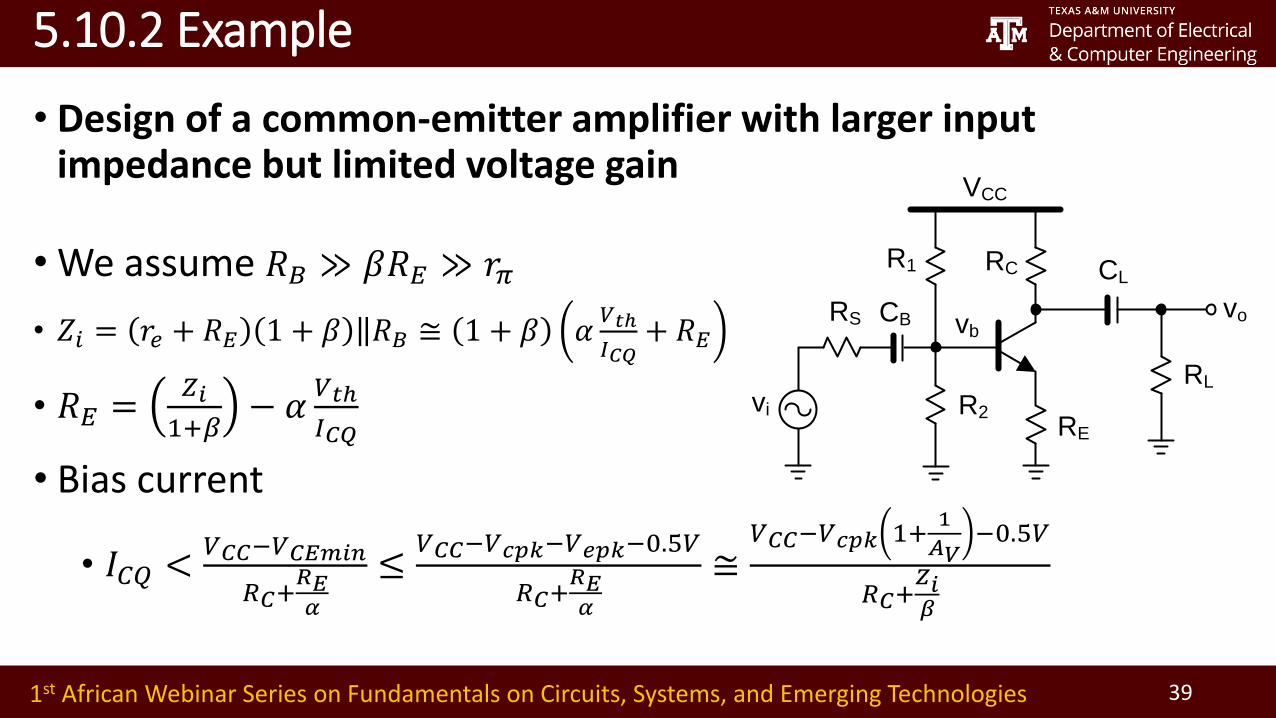
5.10.2 Example
• Design of a common-emitter amplifier with larger input impedance but limited voltage gain
• We assume 𝑅𝐵 ≫ 𝛽𝑅𝐸 ≫ 𝑟𝜋
• 𝑍𝑖 = 𝑟𝑒 + 𝑅𝐸 1 + 𝛽 𝑅𝐵 ≅ 1 + 𝛽 𝛼𝑉𝑡ℎ
𝐼𝐶𝑄+ 𝑅𝐸
• 𝑅𝐸 =𝑍𝑖
1+𝛽− 𝛼
𝑉𝑡ℎ
𝐼𝐶𝑄
• Bias current
• 𝐼𝐶𝑄 <𝑉𝐶𝐶−𝑉𝐶𝐸𝑚𝑖𝑛
𝑅𝐶+𝑅𝐸𝛼
≤𝑉𝐶𝐶−𝑉𝑐𝑝𝑘−𝑉𝑒𝑝𝑘−0.5𝑉
𝑅𝐶+𝑅𝐸𝛼
≅𝑉𝐶𝐶−𝑉𝑐𝑝𝑘 1+
1
𝐴𝑉−0.5𝑉
𝑅𝐶+𝑍𝑖𝛽
VCC
RC
vi
R1
R2
vb
RE
CBRS
RL
vo
CL

401st African Webinar Series on Fundamentals on Circuits, Systems, and Emerging Technologies
5.10.2 Example
• Bias current upper limit is
• 𝐼𝐶𝑄 >𝑉𝑜𝑝𝑘
𝑅𝐶
• Gain is given by
•𝑣𝑜
𝑣𝑏= 𝛼
𝑅𝐶 𝑅𝐿
𝑟𝑒+𝑅𝐸= 𝛼
𝑅𝐶 𝑅𝐿𝑉𝑡ℎ𝐼𝐶𝑄
+𝑅𝐸
• When source resistance is included
•𝑣𝑜
𝑣𝑖=
𝑣𝑜
𝑣𝑏
𝑣𝑏
𝑣𝑖=
𝑍𝑖
𝑍𝑖+𝑅𝑆𝛼
𝑅𝐶 𝑅𝐿
𝑟𝑒+𝑅𝐸≅ 𝛼
𝑅𝐶 𝑅𝐿
𝑟𝑒+𝑅𝐸+𝑅𝑆
1+𝛽
- (5)
• Harmonics are generated from 𝑒𝑣𝑏𝑒𝑉𝑡ℎ = 1 +
𝑣𝑏𝑒
𝑉𝑡ℎ+
1
2
𝑣𝑏𝑒
𝑉𝑡ℎ
2+
1
6
𝑣𝑏𝑒
𝑉𝑡ℎ
3+. .
VCC
RC
vi
R1
R2
vb
RE
CBRS
RL
vo
CL

411st African Webinar Series on Fundamentals on Circuits, Systems, and Emerging Technologies
5.10.2 Example
• We limit 𝑣𝑏𝑒−𝑝𝑘
𝑉𝑡ℎ< 1/4 to limit harmonics
•𝑣𝑏𝑒−𝑝𝑘
𝑣𝑖−𝑝𝑘=
𝑍𝑖
𝑍𝑖+𝑅𝑆
𝑟𝑒
𝑟𝑒+𝑅𝐸=
𝑟𝑒
𝑟𝑒+𝑅𝐸+𝑅𝑆
1+𝛽
•𝑣𝑜−𝑝𝑘
𝑣𝑖−𝑝𝑘≅ 𝛼
𝑅𝐶 𝑅𝐿
𝑟𝑒
𝑣𝑏𝑒−𝑝𝑘
𝑣𝑖−𝑝𝑘=
𝐼𝐶𝑄 𝑅𝐶 𝑅𝐿
𝑉𝑡ℎ
𝑣𝑏𝑒−𝑝𝑘
𝑣𝑖−𝑝𝑘
• Equation rearranges to 𝐼𝐶𝑄 ≅𝑉𝑡ℎ
𝑅𝐶 𝑅𝐿
𝑣𝑖−𝑝𝑘
𝑣𝑏𝑒−𝑝𝑘𝐴𝑣 -
• Then
• 𝐼𝐶𝑄 ≅𝛽𝑉𝑡ℎ
𝑍𝑖
𝑣𝑖−𝑝𝑘
𝑣𝑏𝑒−𝑝𝑘− 1
VCC
RC
vi
R1
R2
vb
RE
CBRS
RL
vo
CL

421st African Webinar Series on Fundamentals on Circuits, Systems, and Emerging Technologies
5.10.2 Example
• Plot made for • 𝛽 = 200, Zi 150 k,
RL = 10 k, Vomax = 1 Vpk, and VCC = 5V
• There is no solution exist for 𝑉𝑐𝑐 = 10𝑉 and 𝐴𝑉 = 10
0
0.2
0.4
0.6
0.8
1
1.2
1.4
1.6
1.8
2
2000 4000 6000 8000 10000 12000
Col
lect
or c
urre
nt (m
A)
Collector resistance RC
Equation 5.66; VCC=10
Equation 5.66; VCC=5
Equation 5.72b; |AV|=10
Equation 5.72b; |AV|=5
Equation 5.73; Zi=150kΩAcceptable solution
Equation (3); Vcc=10V
Equation (7); |𝐴𝑉|=10Equation (7); |𝐴𝑉|=5
Equation (8); 𝑍𝑖 = 150𝑘Ω Equation (3); Vcc=5V
𝐼𝐶𝑄
𝛼𝑉𝑡ℎ

431st African Webinar Series on Fundamentals on Circuits, Systems, and Emerging Technologies
30 dB gain amplifier driving a load of 10kΩRelative small input impedance ( r)Robust?Tolerant to temperature and beta variations?

441st African Webinar Series on Fundamentals on Circuits, Systems, and Emerging Technologies
30 dB gain amplifier driving a load of 10kΩ
Voltage at collector terminal DC level is around 3.12V Gain 40*1.88 *10/22= 34dB
Voltage at the load impedance

451st African Webinar Series on Fundamentals on Circuits, Systems, and Emerging Technologies
Temperature variations: -500, 270 and 1000

461st African Webinar Series on Fundamentals on Circuits, Systems, and Emerging Technologies
Source Degeneration benefits: More stable operating point Better linearity More stable frequency response More accurate voltage gain Higher input impedance
Source Degeneration drawbacks: Reduced voltage gain
R6 and R5 make the operating point more stable and less sensitive to both T and variations
R6 stabilize the voltage and increase amplifier’s input impedance
Temperature variations: -500, 270 and 1000
Source degenerated amplifier: Temperature sensitivity

471st African Webinar Series on Fundamentals on Circuits, Systems, and Emerging Technologies
Source Degeneration benefits: More stable operating point. The DC voltage at the collector varies from 2.6V till 3.3V; Reduced voltage gain: Voltage gain reduces, and determined by overall load resistance and overall emitter
resistance ~ 14dB; Voltage gain is little sensitive to PVT (process-voltage-temperature) variations; Input impedance >> r

481st African Webinar Series on Fundamentals on Circuits, Systems, and Emerging Technologies
Without Source Degeneration With Source Degeneration

491st African Webinar Series on Fundamentals on Circuits, Systems, and Emerging Technologies
Without Source Degeneration With Source Degeneration

501st African Webinar Series on Fundamentals on Circuits, Systems, and Emerging Technologies
Summary
• DC and AC Analysis of BJT based circuits
• Different Amplifier configuration analysis• Common-Emitter, Common – Base and Common Collector
• Design procedure based on circuit constrains
• Cascade of amplifiers and their analysis

511st African Webinar Series on Fundamentals on Circuits, Systems, and Emerging Technologies
Field-effect MOS transistors

521st African Webinar Series on Fundamentals on Circuits, Systems, and Emerging Technologies
Outline
• CMOS Transistors Fundamentals.
• MOS Transistor Operating in the Saturation Region.
• Common-Source Amplifier.
• Common-Source Amplifier with Source Degeneration.
• Common-gate Amplifier.
• Common-Drain Amplifier.
• Design Considerations and Examples.

531st African Webinar Series on Fundamentals on Circuits, Systems, and Emerging Technologies
6.1 CMOS Transistors Fundamentals.
• CMOS transistors → 4 terminal devices• Source(S), Drain(D), Gate(G), Bulk(B)
• N-MOS Transistor• Source & Drain → N-type doping
• Bulk (Substrate) → P-type doping
• Gate → Metal terminal, Separated with Gate Oxide (Insulator material. Eg: SiO2)
• Bulk → B-S and B-D p-n junction reverse biased• Bulk → Lowest potential in device
B S G D
iD
Thin SiOx
N+
N+
N+
P-type Substrate
Metal Channel Thick
Oxide
G DSB
L
W
vG
VD
VS
VB
iD
N-MOS Cross section view
N-MOS Top view
N-MOS Symbol

541st African Webinar Series on Fundamentals on Circuits, Systems, and Emerging Technologies
6.3 MOS Transistor Operating in the Saturation Region
• Transistor in saturation region • 𝑉𝐺𝑆 > 𝑉𝑇 and 𝑉𝐷𝑆 > 𝑉𝐷𝑆𝐴𝑇
• Drain current equation
• 𝐼DS =𝐾𝑛
2
𝑊
𝐿𝑉𝐺𝑆 − 𝑉𝑇
2 1 + 𝜆𝑉𝐷𝑆
• Here 𝜆 ≅1
𝐿𝑉𝑒𝑎𝑟𝑙𝑦
• Also written as 𝐼DS =𝛽
21 + 𝜆𝑉𝐷𝑆 𝑉𝐷𝑆𝐴𝑇
2
D
VGS
VDS
lID
Triode region
Saturation region
VDS=VDSAT
vg
vd
vs
vb
ids
551st African Webinar Series on Fundamentals on Circuits, Systems, and Emerging Technologies
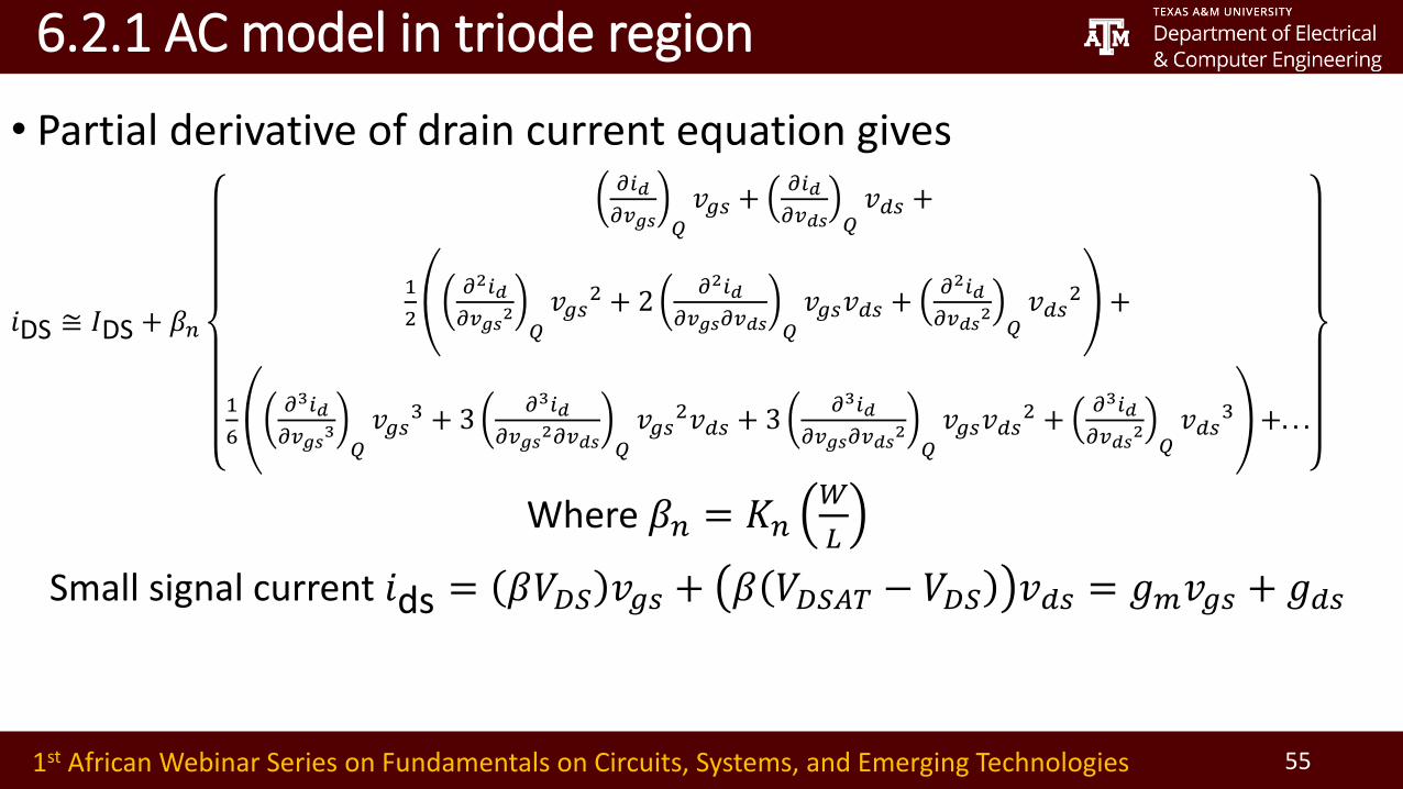
6.2.1 AC model in triode region
• Partial derivative of drain current equation gives
𝑖DS ≅ 𝐼DS + 𝛽𝑛
𝜕𝑖𝑑
𝜕𝑣𝑔𝑠 𝑄
𝑣𝑔𝑠 +𝜕𝑖𝑑
𝜕𝑣𝑑𝑠 𝑄𝑣𝑑𝑠 +
1
2
𝜕2𝑖𝑑
𝜕𝑣𝑔𝑠2
𝑄
𝑣𝑔𝑠2 + 2
𝜕2𝑖𝑑
𝜕𝑣𝑔𝑠𝜕𝑣𝑑𝑠 𝑄
𝑣𝑔𝑠𝑣𝑑𝑠 +𝜕2𝑖𝑑
𝜕𝑣𝑑𝑠2
𝑄𝑣𝑑𝑠
2 +
1
6
𝜕3𝑖𝑑
𝜕𝑣𝑔𝑠3
𝑄
𝑣𝑔𝑠3 + 3
𝜕3𝑖𝑑
𝜕𝑣𝑔𝑠2𝜕𝑣𝑑𝑠 𝑄
𝑣𝑔𝑠2𝑣𝑑𝑠 + 3
𝜕3𝑖𝑑
𝜕𝑣𝑔𝑠𝜕𝑣𝑑𝑠2
𝑄
𝑣𝑔𝑠𝑣𝑑𝑠2 +
𝜕3𝑖𝑑
𝜕𝑣𝑑𝑠2
𝑄𝑣𝑑𝑠
3 +. . .
Where 𝛽𝑛 = 𝐾𝑛𝑊
𝐿
Small signal current 𝑖ds = 𝛽𝑉𝐷𝑆 𝑣𝑔𝑠 + 𝛽 𝑉𝐷𝑆𝐴𝑇 − 𝑉𝐷𝑆 𝑣𝑑𝑠 = 𝑔𝑚𝑣𝑔𝑠 + 𝑔𝑑𝑠

561st African Webinar Series on Fundamentals on Circuits, Systems, and Emerging Technologies
6.3.1 Small – Signal Model
• Transconductance
𝑔𝑚 = 𝜕𝑖𝑑𝜕𝑣𝑔𝑠
𝑄
= 𝛽𝑉𝐷𝑆𝐴𝑇 1 + 𝜆𝑉𝐷𝑆
• if 𝜆𝑉𝐷𝑆𝐴𝑇 ≪ 1 then we can use 𝑔𝑚 ≅ 𝛽𝑉𝐷𝑆𝐴𝑇
• Drain – Source conductance (output impedance)
𝑔𝑑𝑠 = 𝜕𝑖𝑑𝜕𝑣𝑑𝑠 𝑄
=𝛽
2𝑉𝐷𝑆𝐴𝑇
2 ⋅ 𝜆 ≅ 𝐼𝐷𝑆 ⋅ 𝜆
• Gate-Source capacitance
𝐶𝑔𝑠 ≅ 𝑊𝐿𝜖𝑜𝑥
𝑡𝑜𝑥
vs
vdids
gmvgs
+
vgs
-
vg
gdsCgs
ig=0
1
vs
vd
gmvgs
+
vgs
-
gds
gm
ig=0
Cgs
vg
1
1
𝜋 - model
𝑇 - model

571st African Webinar Series on Fundamentals on Circuits, Systems, and Emerging Technologies
6.3.2 Harmonic Distortion
• Earlier discussed equation should be used to calculate harmonic terms
𝐻𝐷2 =1
1 −𝜆𝑉𝐷𝑆𝐴𝑇
8 1 + 𝜆𝑉𝐷𝑆
𝑣𝑑𝑠𝑣𝑔𝑠
⋅𝑉𝑔𝑠−𝑝𝑘
4𝑉𝐷𝑆𝐴𝑇
• Note that HD2 for BJT was 1
4
𝑉𝑝𝑘
𝑉𝑡ℎ, where 𝑉𝑡ℎ = 25𝑚𝑉
• BJT has higher HD2 than MOSFET
𝐻𝐷3 =𝐴𝑉𝜆𝑉𝐷𝑆𝐴𝑇
12 1 + 𝜆𝑉𝐷𝑆 +𝐴𝑉𝜆𝑉𝐷𝑆𝐴𝑇
2
𝑣𝑔𝑠−𝑝𝑘
𝑉𝐷𝑆𝐴𝑇
2
581st African Webinar Series on Fundamentals on Circuits, Systems, and Emerging Technologies
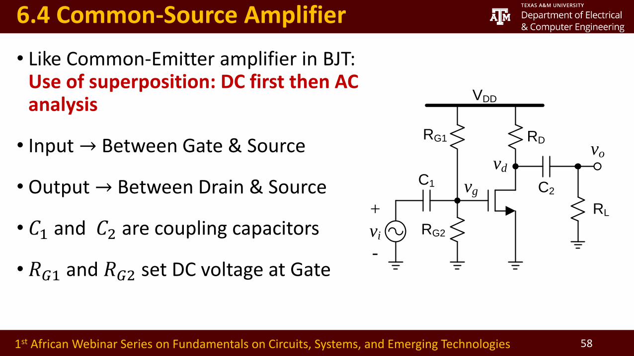
6.4 Common-Source Amplifier
• Like Common-Emitter amplifier in BJT: Use of superposition: DC first then AC analysis
• Input → Between Gate & Source
• Output → Between Drain & Source
• 𝐶1 and 𝐶2 are coupling capacitors
• 𝑅𝐺1 and 𝑅𝐺2 set DC voltage at Gate
C1 C2
RG1
RG2
RD
RL+
vi
-
vo
VDD
vg
vd

591st African Webinar Series on Fundamentals on Circuits, Systems, and Emerging Technologies
6.4.1 DC analysis: Notice that IG=0
• Solve these equations to find VG, IDS and VDS
𝑉𝐺 = 𝑉𝐺𝑆 =𝑅𝐺2
𝑅𝐺1+𝑅𝐺2𝑉𝐷𝐷
𝐼DS =𝛽
2𝑉𝐺𝑆 − 𝑉𝑇
2
𝑉DS = 𝑉𝐷𝐷 − 𝐼DS𝑅𝐷
IG=0
IDS
VGSVT
2
2TGSDS VVI
GV
Q
IDS
RG
RD
VDD
VG
+
-
VGS+
-
VD
IDS

601st African Webinar Series on Fundamentals on Circuits, Systems, and Emerging Technologies
6.4.2 AC analysis: routine techniques
𝑣𝑜
𝑣𝑖= −
𝑠𝑅𝐺𝐶1
1 + 𝑠𝑅𝐺(𝐶1 + 𝐶𝑔𝑠)
𝑠 𝑅𝐷||𝑟𝑑𝑠 𝐶2
1 + 𝑠 𝑅𝐷||𝑟𝑑𝑠 + 𝑅𝐿 𝐶2
𝑔𝑚𝑅𝐿
Further simplifies to
𝑣𝑜
𝑣𝑖= −
𝑠𝜔𝑍1
1 +𝑠
𝜔𝑃1
𝑠𝜔𝑍2
1 +𝑠
𝜔𝑃1
𝑔𝑚𝑅𝐿
C1
C2
RG=
RG1||RG2
RL
+
vi
-
vo
vd
vs
gmvgs
+
-vgs
rs=
1/gm
i=0
Cgs
Zi
vg
rds||RD
Here 𝜔𝑍1 =1
𝑅𝐺𝐶1; 𝜔𝑍2 =
1
𝑅𝐷||𝑟𝑑𝑠 𝐶2
𝜔𝑃1 =1
𝑅𝐺 𝐶1+𝐶𝑔𝑠; 𝜔𝑍2 =
1
𝑅𝐷||𝑟𝑑𝑠 𝐶2
AC Small signal equivalent circuit

611st African Webinar Series on Fundamentals on Circuits, Systems, and Emerging Technologies
6.4.2 AC analysis: conventional analysis
• If 𝐶1 ≫ 𝐶𝑔𝑠 and 𝜔 ≫𝜔𝑃1, 𝜔𝑃2 then
𝑣𝑜
𝑣𝑖= −𝑔𝑚 ⋅ 𝑅𝐷||𝑟𝑑𝑠||𝑅𝐿
• If 𝐶1 and 𝐶𝑔𝑠 are comparable and 𝜔 ≫𝜔𝑃1, 𝜔𝑃2 then
𝑣𝑔𝑠
𝑣𝑖≈
𝐶1
𝐶1 + 𝐶𝑔𝑠
𝑣𝑜
𝑣𝑖= −𝑔𝑚 ⋅ 𝑅𝐷 𝑟𝑑𝑠 𝑅𝐿
𝐶1
𝐶1+𝐶𝑔𝑠
(log)
40 dB/decade
P1 P2
20 dB/decade
mLdsD
gs
gR||r||RCC
Clog
1
11020
dBi
o
v
v

621st African Webinar Series on Fundamentals on Circuits, Systems, and Emerging Technologies
6.4.3 Practical Design Considerations
• Transistor should remain in Saturation region at all time instances
• For negative peak of output
𝑉𝐷𝑆 = 𝑉𝐷𝐷 − 𝐼𝐷𝑆𝑅𝐷 > 𝑉𝐷𝑆𝐴𝑇 + 𝑣𝑜−𝑝𝑘
• For positive peak of output
𝑉𝐷𝑆 = 𝑉𝐷𝐷 − 𝐼𝐷𝑆𝑅𝐷 < 𝑉𝐷𝐷 − 𝑣𝑜−𝑝𝑘
• Combining two inequalities we get 𝑉𝐷𝐷 − 𝑉𝐷𝑆𝐴𝑇 − 𝑣𝑜−𝑝𝑘
𝑅𝐷> 𝐼𝐷𝑆 >
𝑣𝑜−𝑝𝑘
𝑅𝐷
Vomax
Vomax
VDD
IDQRD
VDSat

631st African Webinar Series on Fundamentals on Circuits, Systems, and Emerging Technologies
6.4.3 Practical Design Considerations
• 𝑣𝑖−𝑝𝑘 < 𝑉𝐷𝑆𝐴𝑇 to avoid clipping at input side
vGS
Q
VT
VDSAT
VGS
iDS
VDD
vDS
VDS=VDSAT
Q1
Q2
vGS1
vGS2
iDS
Static load
line
VDD/RD
Input side
output side
•𝑉𝐷𝐷−𝑉𝐷𝑆𝐴𝑇−𝑣𝑜−𝑝𝑘
𝑅𝐷> 𝐼𝐷𝑆 >
𝑣𝑜−𝑝𝑘
𝑅𝐷
to avoid clipping at output side

641st African Webinar Series on Fundamentals on Circuits, Systems, and Emerging Technologies
6.4.4 Harmonic Distortion
Using earlier defined relation
𝐻𝐷2 ≅
𝐶1𝐶1 + 𝐶𝑔𝑠
1 −𝜆𝑉𝐷𝑆𝐴𝑇
8 1 + 𝜆𝑉𝐷𝑆
𝑣𝑑𝑠𝑣𝑔𝑠
𝑣𝑖−𝑝𝑘
4𝑉𝐷𝑆𝐴𝑇
With 𝑣𝑑𝑠
𝑣𝑔𝑠≅ 𝑔𝑚
𝑟𝑑𝑠𝑅𝐿
𝑟𝑑𝑠+𝑅𝐿; If we also make the approximation 𝜆 is very small
𝐻𝐷2 ≅𝐶1
𝐶1+𝐶𝑔𝑠
𝑣𝑖−𝑝𝑘
4𝑉𝐷𝑆𝐴𝑇=
𝐶1
𝐶1+𝐶𝑔𝑠
𝑖𝑑−𝑝𝑘
8𝐼𝐷𝑆
We have 𝑖𝑑−𝑝𝑘
𝑣𝑑−𝑝𝑘= 𝑔𝑚 =
2𝐼𝐷𝑆
𝑉𝐷𝑆𝐴𝑇
Minimum value of 𝐼𝐷 required can be calculated as
𝐼𝐷𝑆 ≥𝐶1
𝐶1 + 𝐶𝑔𝑠
𝑣𝑜−𝑝𝑘
8 ⋅ 𝐻𝐷2 ⋅ 𝑅𝐿||𝑅𝐷
651st African Webinar Series on Fundamentals on Circuits, Systems, and Emerging Technologies
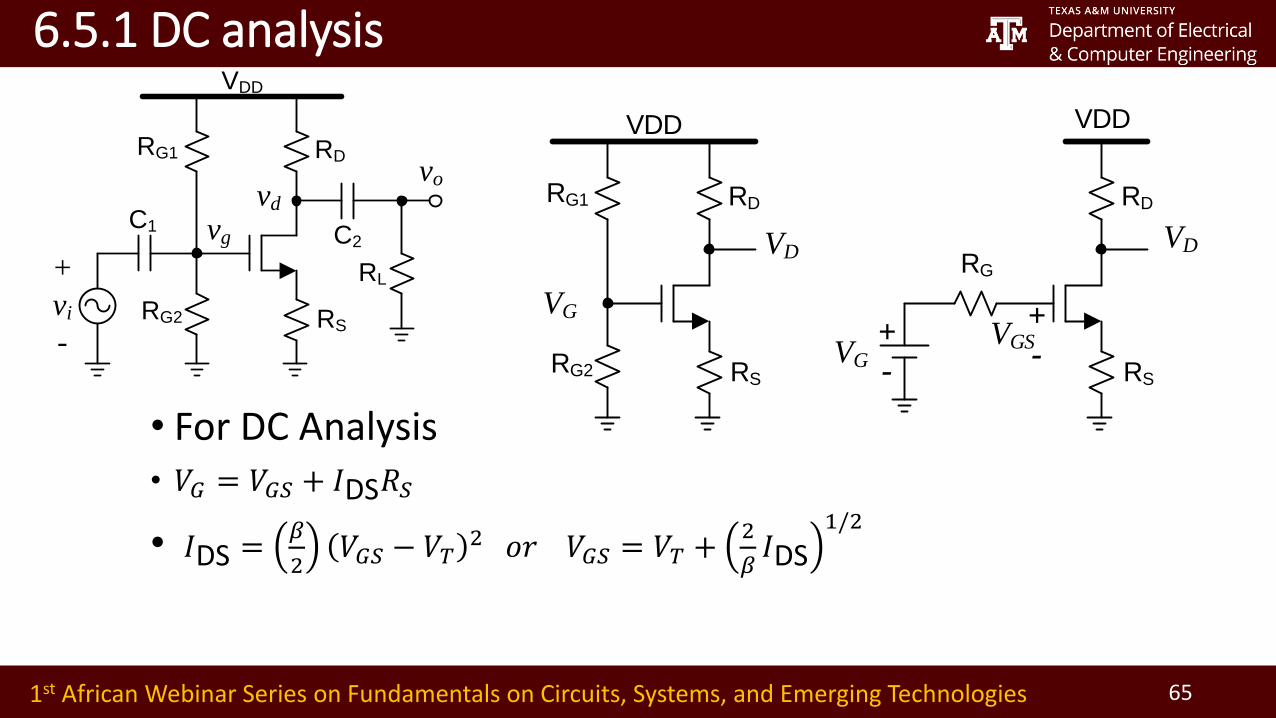
6.5.1 DC analysis
• For DC Analysis• 𝑉𝐺 = 𝑉𝐺𝑆 + 𝐼DS𝑅𝑆
• 𝐼DS =𝛽
2𝑉𝐺𝑆 − 𝑉𝑇
2 𝑜𝑟 𝑉𝐺𝑆 = 𝑉𝑇 +2
𝛽𝐼DS
1/2
C1 C2
RG1
RG2
RD
RL+
vi
-
vo
VDD
vg
vd
RS
RG1
RG2
RD
VDD
VG
VD
RS
RG
RD
VDD
VGRS
+
-
VGS+
-
VD

661st African Webinar Series on Fundamentals on Circuits, Systems, and Emerging Technologies
6.5.1 DC analysis
• We have 𝑉𝐺 = 𝑉𝐺𝑆 + 𝐼DS𝑅𝑆
• 𝐼DS =𝛽
2𝑉𝐺𝑆 − 𝑉𝑇
2 𝑜𝑟 𝑉𝐺𝑆 = 𝑉𝑇 +2
𝛽𝐼DS
1/2
• Combining two equations we get
𝐼DS +1
𝑅𝑆
2
𝛽𝐼DS −
𝑉𝐺 − 𝑉𝑇
𝑅𝑆= 0
• Solving this equations and picking the meaningful solution we get
𝐼DS =1
𝛽𝑅𝑆2 1 + 𝛽𝑅𝑆 𝑉𝐺 − 𝑉𝑇 − 1 + 2𝛽𝑅𝑆 𝑉𝐺 − 𝑉𝑇
Operating point
VGSVT
2
2TGSDS VVI
S
GSGDS
R
VVI
S
GDS
R
VI
GV
Q
IDS
RG1
RG2
RD
VDD
VG
VD
RS
RG
RD
VDD
VGRS
+
-
VGS+
-
VD
671st African Webinar Series on Fundamentals on Circuits, Systems, and Emerging Technologies
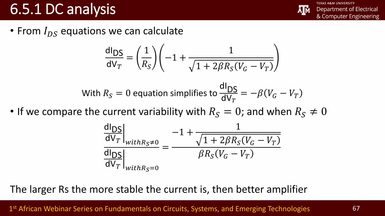
6.5.1 DC analysis
• From 𝐼𝐷𝑆 equations we can calculate
dIDSdV𝑇
=1
𝑅𝑆−1 +
1
1 + 2𝛽𝑅𝑆 𝑉𝐺 − 𝑉𝑇
With 𝑅𝑆 = 0 equation simplifies to dIDSdV𝑇
= −𝛽 𝑉𝐺 − 𝑉𝑇
• If we compare the current variability with 𝑅𝑆 = 0; and when 𝑅𝑆 ≠ 0
dIDSdV𝑇 𝑤𝑖𝑡ℎ𝑅𝑆≠0
dIDSdV𝑇 𝑤𝑖𝑡ℎ𝑅𝑆=0
=
−1 +1
1 + 2𝛽𝑅𝑆 𝑉𝐺 − 𝑉𝑇
𝛽𝑅𝑆 𝑉𝐺 − 𝑉𝑇
The larger Rs the more stable the current is, then better amplifier

681st African Webinar Series on Fundamentals on Circuits, Systems, and Emerging Technologies
6.5.2 AC analysis
• Voltage division at input gives𝑣𝑔
𝑣𝑖𝑛=
𝑠𝑅𝐺𝐶1
1 + 𝑠𝑅𝐺𝐶1
• KCL analysis at drain node gives
𝑣𝑑
𝑣𝑔= −
𝑅𝐷
𝑟𝑆 + 𝑅𝑆
1 + 𝑠𝑅𝐿𝐶2
1 + 𝑠 𝑅𝐷 + 𝑅𝐿 𝐶2
• Voltage division at output node gives
𝑣0
𝑣𝑑=
𝑠𝑅𝐿𝐶2
1 + 𝑠𝑅𝐿𝐶2
C1
C2
RG=
RG1||RG2
RL+
vi
-
vo
vd
vs
gmvgs
+
-vgs
rs=1/gm
i=0
Zi
vg
RS
RD
idAC small signal equivalent
• Total gain 𝑣0
𝑣𝑖𝑛= −
𝑅𝐷
𝑟𝑆 + 𝑅𝑆
𝑠𝑅𝐺𝐶1
1 + 𝑠𝑅𝐺𝐶1
𝑠𝑅𝐿𝐶2
1 + 𝑠 𝑅𝐷 + 𝑅𝐿 𝐶2
• At high frequency𝑣0
𝑣𝑖𝑛
≅ −𝑅𝐷||𝑅𝐿
𝑟𝑆 + 𝑅𝑆

691st African Webinar Series on Fundamentals on Circuits, Systems, and Emerging Technologies
6.5.3 Nonlinearity analysis
• Taylor series expansion of drain current gives
𝑖𝐷𝑆 =1 + 2𝛽𝑅𝑆 𝑉𝐺 − 𝑉𝑇 − 1
2
2𝛽𝑅𝑆2 +
1 − 1 + 2𝛽𝑅𝑆 𝑉𝐺 − 𝑉𝑇−
12
𝑅𝑆𝑣𝑖𝑛 +
𝛽
2(1 + 2𝛽𝑅𝑆 𝑉𝐺 − 𝑉𝑇 )−
32𝑣𝑖𝑛
2 −𝛽2𝑅𝑆
21 + 2𝛽𝑅𝑆 𝑉𝐺 − 𝑉𝑇
−52𝑣𝑖𝑛
3 + ⋯
• Harmonic distortion simplifies to equation
𝐻𝐷2 =1
1 + 2𝛽𝑅𝑆 𝑉𝐺 − 𝑉𝑇
𝛽𝑅𝑆
4 1 + 2𝛽𝑅𝑆 𝑉𝐺 − 𝑉𝑇1/2
− 1𝑣𝑖𝑛
DC Linear term
2nd Order term 3rd Order term
Find expression for HD3 in same way
701st African Webinar Series on Fundamentals on Circuits, Systems, and Emerging Technologies
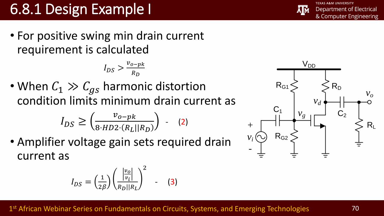
6.8.1 Design Example I
• For positive swing min drain current requirement is calculated
𝐼𝐷𝑆 >𝑣𝑜−𝑝𝑘
𝑅𝐷
• When 𝐶1 ≫ 𝐶𝑔𝑠 harmonic distortion condition limits minimum drain current as
𝐼𝐷𝑆 ≥𝑣𝑜−𝑝𝑘
8⋅𝐻𝐷2⋅ 𝑅𝐿||𝑅𝐷- (2)
• Amplifier voltage gain sets required drain current as
𝐼𝐷𝑆 =1
2𝛽
𝑣𝑜𝑣𝑖
𝑅𝐷||𝑅𝐿
2
- (3)
C1 C2
RG1
RG2
RD
RL+
vi
-
vo
VDD
vg
vd

711st African Webinar Series on Fundamentals on Circuits, Systems, and Emerging Technologies
0.0E+00
5.0E-04
1.0E-03
1.5E-03
2.0E-03
5.0E+03 1.0E+04 1.5E+04 2.0E+04 2.5E+04
Dra
in C
urr
ent
Drain Resistance
Eq. 3Av=6
Eq. 3Av=4
Eq. 1
Eq. 2
6.8.1 Design Example I
Notice that Gain = 4 has a region of possible solutions
Acceptable 𝑅𝐷 region is 6.5𝑘Ω to 15𝑘Ω 𝐼𝐷 in the region 380𝜇𝐴 -1050𝜇𝐴
Gain = 6 doesn’t have a feasible solution region

721st African Webinar Series on Fundamentals on Circuits, Systems, and Emerging Technologies
6.8.1 Design Example I
• Circuit is simulated in LT spice with 𝑅𝐷 = 10𝑘Ω and 𝐼𝐷 = 600𝜇𝐴
Gain vs frequency plot

731st African Webinar Series on Fundamentals on Circuits, Systems, and Emerging Technologies
6.8.1 Design Example I
Transient response for 1kHz input and amplitude 60𝑚𝑉𝑝𝑘
Signal swing at Drain
Signal swing at Output node
741st African Webinar Series on Fundamentals on Circuits, Systems, and Emerging Technologies
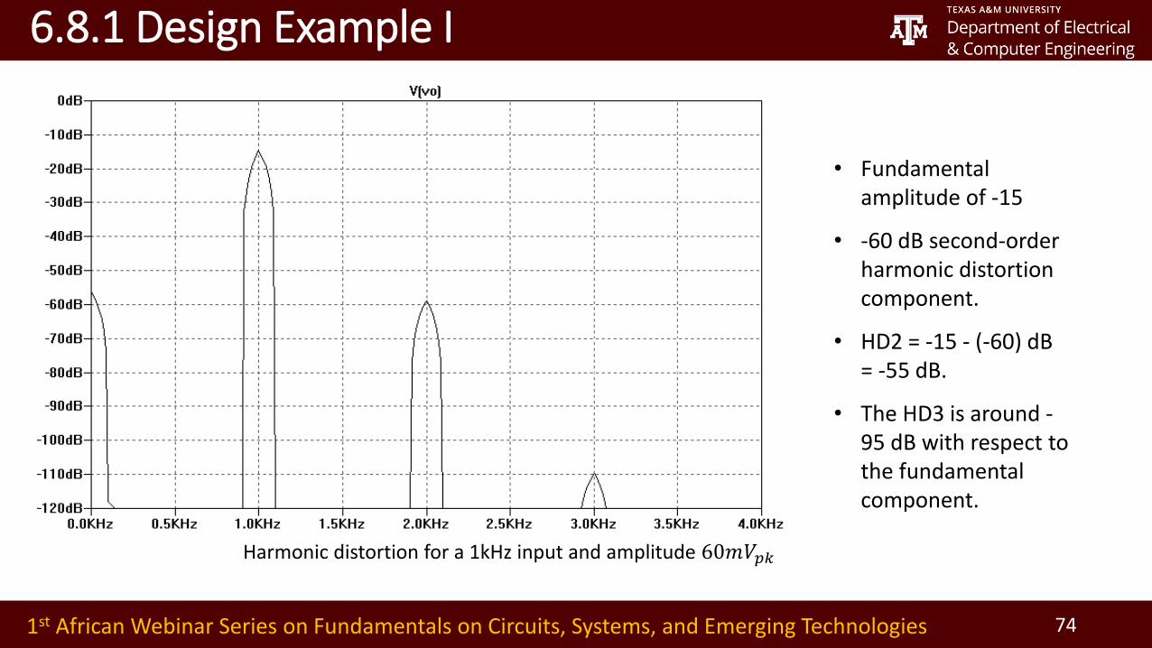
6.8.1 Design Example I
Harmonic distortion for a 1kHz input and amplitude 60𝑚𝑉𝑝𝑘
• Fundamental amplitude of -15
• -60 dB second-order harmonic distortion component.
• HD2 = -15 - (-60) dB = -55 dB.
• The HD3 is around -95 dB with respect to the fundamental component.

751st African Webinar Series on Fundamentals on Circuits, Systems, and Emerging Technologies
6.8.1 Design Example II
• Sensitivity of non source degenerated amplifier to threshold voltage
𝛥𝐼𝐷𝐼𝐷
𝛥𝑉𝑇𝑉𝑇
≅
𝑑𝐼𝐷𝐼𝐷
𝑑𝑉𝑇𝑉𝑇
=𝑉𝑇
𝐼𝐷
𝑑𝐼𝐷𝑑𝑉𝑇
= −2𝑉𝑇
𝑉𝐺𝑆 − 𝑉𝑇
• 𝑉𝑇 variations can be as high as ±20%• Higher drain current variations
•𝛥𝐼𝐷
𝐼𝐷≅ −
2𝑉𝑇
𝑉𝐺𝑆−𝑉𝑇
𝛥𝑉𝑇
𝑉𝑇
Common-source Amplifier with DC Source Degeneration
C1 C2
RG1
RG2
RD
RL+
vi
-
vo
VDD
vg
vd
RS

761st African Webinar Series on Fundamentals on Circuits, Systems, and Emerging Technologies
6.8.1 Design Example II
• Drain current sensitivity for source degenerated current source
𝛥𝐼𝐷𝐼𝐷
𝛥𝑉𝑇𝑉𝑇
≅dIDSdV𝑇
𝑉𝑇
𝐼DS= −
1+2𝛽𝑅𝑆 𝑉𝐺−𝑉𝑇 −1
1+2𝛽𝑅𝑆 𝑉𝐺−𝑉𝑇
𝑉𝑇
𝑅𝑆𝐼DS
• Higher the 𝑅𝑠 less 𝐼𝐷𝑆 variations with 𝑉𝑇
• But higher voltage drop across 𝑅𝑆
•𝛥𝐼𝐷
𝐼𝐷≅
1− 1+2𝛽𝑅𝑆 𝑉𝐺𝑆−𝑉𝑇+𝑅𝑆𝐼DS
1+2𝛽𝑅𝑆 𝑉𝐺𝑆−𝑉𝑇+𝑅𝑆𝐼DS
𝑉𝑇
𝑅𝑆𝐼DS
𝛥𝑉𝑇
𝑉𝑇
-2.0E+0
-1.8E+0
-1.6E+0
-1.4E+0
-1.2E+0
-1.0E+0
-8.0E-1
-6.0E-1
-4.0E-1
0 1000 2000 3000 4000 5000
Sen
siti
vity
Fu
nct
ion
Source Resistance

771st African Webinar Series on Fundamentals on Circuits, Systems, and Emerging Technologies
6.8.1 Design Example II
• At the lowest voltage swing at output node
𝑉DS = 𝑉𝐷𝐷 − 𝐼DS 𝑅𝑆 + 𝑅𝐷 > 𝑣𝑜−𝑝𝑘 + 𝑉𝐺𝑆 − 𝑉𝑇
• If we assume 𝐼𝐷𝑆𝑅𝑠 = 2.5𝑉
𝑉DS = 𝑉𝐷𝐷 − 2.5 − 𝑣𝑜−𝑝𝑘 > 𝐼DS𝑅𝐷 + 𝑉𝐺𝑆 − 𝑉𝑇
• Proceeding as previous example to find sensitivity
𝐼𝐷𝑆 ≤𝑉𝐷𝐷−2.5−𝑣𝑜−𝑝𝑘
𝑅𝐷+
1
2𝛽𝑅𝐷2 −
1
2𝛽𝑅𝐷
2
- (4)
Vomax
Vomax
VDD
IDQRD
VDSQ-VDSat

781st African Webinar Series on Fundamentals on Circuits, Systems, and Emerging Technologies
0.0E+00
5.0E-04
1.0E-03
1.5E-03
2.0E-03
5.0E+03 1.0E+04 1.5E+04 2.0E+04 2.5E+04
Dra
in C
urr
ent
Drain Resistance
6.8.1 Design Example II
• No solution exists for 𝐴𝑣 = 6 or higher
• Range of resistance = 7𝑘Ω − 13𝑘Ω
• Acceptable range of drain current is 400𝜇𝐴 − 850𝜇𝐴
Eq. 3Av=6
Eq. 3Av=4
Eq. 4
Eq. 2

791st African Webinar Series on Fundamentals on Circuits, Systems, and Emerging Technologies
Summary
• DC and AC Analysis of MOSFET based circuits
• Different Amplifier configuration analysis
• Common Source Amplifier
• With and without source degeneration
• Design procedure based on circuit constrains
• The design process is multi-dimensional where PVT variations must be considered!

801st African Webinar Series on Fundamentals on Circuits, Systems, and Emerging Technologies
Time for 8 minutes break