Fundamentals of Microelectronicsece.utdallas.edu/~torlak/courses/ee3311/lectures/ch05updated.pdf ·...
35
11/1/2010 1 1 Fundamentals of Microelectronics CH1 Why Microelectronics? CH2 Basic Physics of Semiconductors CH3 Diode Circuits CH4 Physics of Bipolar Transistors CH5 Bipolar Amplifiers CH6 Physics of MOS Transistors CH7 CMOS Amplifiers CH8 Operational Amplifier As A Black Box 2 Chapter 5 Bipolar Amplifiers 5.1 General Considerations 5.2 Operating Point Analysis and Design 5.3 Bipolar Amplifier Topologies 5.4 Summary and Additional Examples
Transcript of Fundamentals of Microelectronicsece.utdallas.edu/~torlak/courses/ee3311/lectures/ch05updated.pdf ·...

11/1/2010
1
1
Fundamentals of Microelectronics
CH1 Why Microelectronics?
CH2 Basic Physics of Semiconductors
CH3 Diode Circuits
CH4 Physics of Bipolar Transistors
CH5 Bipolar Amplifiers
CH6 Physics of MOS Transistors
CH7 CMOS Amplifiers
CH8 Operational Amplifier As A Black Box
2
Chapter 5 Bipolar Amplifiers
5.1 General Considerations
5.2 Operating Point Analysis and Design
5.3 Bipolar Amplifier Topologies
5.4 Summary and Additional Examples

11/1/2010
2
CH5 Bipolar Amplifiers 3
Bipolar Amplifiers
CH5 Bipolar Amplifiers 4
Voltage Amplifier
In an ideal voltage amplifier, the input impedance is infinite and the output impedance zero.
But in reality, input or output impedances depart from their ideal values.

11/1/2010
3
CH5 Bipolar Amplifiers 5
Input/Output Impedances
The figure above shows the techniques of measuring input and output impedances.
x
x
xi
VR =
CH5 Bipolar Amplifiers 6
Input Impedance Example I
When calculating input/output impedance, small-signal analysis is assumed.
πri
v
x
x =

11/1/2010
4
CH5 Bipolar Amplifiers 7
Impedance at a Node
When calculating I/O impedances at a port, we usually ground one terminal while applying the test source to the other terminal of interest.
CH5 Bipolar Amplifiers 8
Impedance at Collector
With Early effect, the impedance seen at the collector is equal to the intrinsic output impedance of the transistor (if emitter is grounded).
ooutrR =

11/1/2010
5
CH5 Bipolar Amplifiers 9
Impedance at Emitter
The impedance seen at the emitter of a transistor is approximately equal to one over its transconductance (if the base is grounded).
)(
1
1
1
∞=
≈
+
=
A
m
out
mx
x
V
gR
rg
i
v
π
CH5 Bipolar Amplifiers 10
Three Master Rules of Transistor Impedances
Rule # 1: looking into the base, the impedance is rππππ if emitter is (ac) grounded.
Rule # 2: looking into the collector, the impedance is ro if emitter is (ac) grounded.
Rule # 3: looking into the emitter, the impedance is 1/gm if base is (ac) grounded and Early effect is neglected.

11/1/2010
6
CH5 Bipolar Amplifiers 11
Biasing of BJT
Transistors and circuits must be biased because (1) transistors must operate in the active region, (2) their small-signal parameters depend on the bias conditions.
CH5 Bipolar Amplifiers 12
DC Analysis vs. Small-Signal Analysis
First, DC analysis is performed to determine operating point and obtain small-signal parameters.
Second, sources are set to zero and small-signal model is used.

11/1/2010
7
CH5 Bipolar Amplifiers 13
Notation Simplification
Hereafter, the battery that supplies power to the circuit is replaced by a horizontal bar labeled Vcc, and input signal is simplified as one node called Vin.
CH5 Bipolar Amplifiers 14
Example of Bad Biasing
The microphone is connected to the amplifier in an attempt to amplify the small output signal of the microphone.
Unfortunately, there’s no DC bias current running thru the transistor to set the transconductance.
11/1/2010
8
CH5 Bipolar Amplifiers 15
Another Example of Bad Biasing
The base of the amplifier is connected to Vcc, trying to establish a DC bias.
Unfortunately, the output signal produced by the microphone is shorted to the power supply.
CH5 Bipolar Amplifiers 16
Biasing with Base Resistor
Assuming a constant value for VBE, one can solve for both IB and IC and determine the terminal voltages of the transistor.
However, bias point is sensitive to ββββ variations.
B
BECC
C
B
BECC
BR
VVI
R
VVI
−=
−= β,

11/1/2010
9
CH5 Bipolar Amplifiers 17
Improved Biasing: Resistive Divider
Using resistor divider to set VBE, it is possible to produce an IC that is relatively independent of ββββ if base current is small.
)exp(21
2
21
2
T
CC
SC
CCX
V
V
RR
RII
VRR
RV
+=
+=
CH5 Bipolar Amplifiers 18
Accounting for Base Current
With proper ratio of R1 and R2, IC can be insensitive to ββββ; however, its exponential dependence on resistor deviations makes it less useful.
−=
T
ThevBThev
SCV
RIVII exp

11/1/2010
10
CH5 Bipolar Amplifiers 19
Emitter Degeneration Biasing
The presence of RE helps to absorb the error in VX so VBE
stays relatively constant.
This bias technique is less sensitive to ββββ (I1 >> IB) and VBE
variations.
20
Design Procedure
Choose an IC to provide the necessary small signal parameters, gm, rππππ, etc.
Considering the variations of R1, R2, and VBE, choose a value for VRE.
With VRE chosen, and VBE calculated, Vx can be determined.
Select R1 and R2 to provide Vx.

11/1/2010
11
CH5 Bipolar Amplifiers 21
Self-Biasing Technique
This bias technique utilizes the collector voltage to provide the necessary Vx and IB.
One important characteristic of this technique is that collector has a higher potential than the base, thus guaranteeing active operation of the transistor.
CH5 Bipolar Amplifiers 22
Self-Biasing Design Guidelines
(1) provides insensitivity to ββββ .
(2) provides insensitivity to variation in VBE .
BECCBE
B
C
VVV
RR
−<<∆
>>β
)2(
)1(

11/1/2010
12
CH5 Bipolar Amplifiers 23
Summary of Biasing Techniques
CH5 Bipolar Amplifiers 24
PNP Biasing Techniques
Same principles that apply to NPN biasing also apply to PNP biasing with only polarity modifications.

11/1/2010
13
CH5 Bipolar Amplifiers 25
Possible Bipolar Amplifier Topologies
Three possible ways to apply an input to an amplifier and three possible ways to sense its output.
However, in reality only three of six input/output combinations are useful.
26
Study of Common-Emitter Topology
Analysis of CE Core
Inclusion of Early Effect
Emitter Degeneration
Inclusion of Early Effect
CE Stage with Biasing

11/1/2010
14
CH5 Bipolar Amplifiers 27
Common-Emitter Topology
CH5 Bipolar Amplifiers 28
Small Signal of CE Amplifier
Cmv
inmm
C
out
in
out
v
RgA
vgvgR
v
v
vA
−=
==−
=
π
Current

11/1/2010
15
CH5 Bipolar Amplifiers 29
Limitation on CE Voltage Gain
Since gm can be written as IC/VT, the CE voltage gain can be written as the ratio of VRC and VT.
VRC is the potential difference between VCC and VCE, and VCE cannot go below VBE in order for the transistor to be in active region.
T
CC
vV
RIA =
T
RC
vV
VA =
T
BECC
vV
VVA
−<
CH5 Bipolar Amplifiers 30
Tradeoff between Voltage Gain and Headroom

11/1/2010
16
CH5 Bipolar Amplifiers 31
I/O Impedances of CE Stage
When measuring output impedance, the input port has to be grounded so that Vin = 0.
πri
vR
X
X
in== C
X
X
outR
i
vR ==
CH5 Bipolar Amplifiers 32
CE Stage Trade-offs

11/1/2010
17
CH5 Bipolar Amplifiers 33
Inclusion of Early Effect
Early effect will lower the gain of the CE amplifier, as it appears in parallel with RC.
OCout
OCmv
rRR
rRgA
||
)||(
=
−=
CH5 Bipolar Amplifiers 34
Intrinsic Gain
As RC goes to infinity, the voltage gain reaches the product of gm and rO, which represents the maximum voltage gain the amplifier can have.
The intrinsic gain is independent of the bias current.
T
A
v
Omv
V
VA
rgA
=
−=

11/1/2010
18
CH5 Bipolar Amplifiers 35
Current Gain
Another parameter of the amplifier is the current gain, which is defined as the ratio of current delivered to the load to the current flowing into the input.
For a CE stage, it is equal to ββββ.
β=
=
CEI
in
out
I
A
i
iA
CH5 Bipolar Amplifiers 36
Emitter Degeneration
By inserting a resistor in series with the emitter, we “degenerate” the CE stage.
This topology will decrease the gain of the amplifier but improve other aspects, such as linearity, and input impedance.

11/1/2010
19
CH5 Bipolar Amplifiers 37
Small-Signal Model
Interestingly, this gain is equal to the total load resistance to ground divided by 1/gm plus the total resistance placed in series with the emitter.
E
m
C
v
Em
Cm
v
Rg
RA
Rg
RgA
+
−=
+−=
1
1
CH5 Bipolar Amplifiers 38
Emitter Degeneration Example I
The input impedance of Q2 can be combined in parallel with RE to yield an equivalent impedance that degenerates Q1.
2
1
||1
πrRg
RA
E
m
C
v
+
−=

11/1/2010
20
CH5 Bipolar Amplifiers 39
Emitter Degeneration Example II
In this example, the input impedance of Q2 can be combined in parallel with RC to yield an equivalent collector impedance to ground.
E
m
C
v
Rg
rRA
+
−=
1
2
1
|| π
CH5 Bipolar Amplifiers 40
Input Impedance of Degenerated CE Stage
With emitter degeneration, the input impedance is increased from rππππ to rππππ + (ββββ+1)RE; a desirable effect.
E
X
X
in
XEXX
A
Rri
vR
iRirv
V
)1(
)1(
++==
++=
∞=
β
β
π
π

11/1/2010
21
CH5 Bipolar Amplifiers 41
Output Impedance of Degenerated CE Stage
Emitter degeneration does not alter the output impedance in this case. (More on this later.)
C
X
X
out
Emin
A
Ri
vR
vRvgr
vvv
V
==
=⇒
++==
∞=
00 ππ
π
ππ
CH5 Bipolar Amplifiers 42
Capacitor at Emitter
At DC the capacitor is open and the current source biases the amplifier.
For ac signals, the capacitor is short and the amplifier is degenerated by RE.

11/1/2010
22
CH5 Bipolar Amplifiers 43
Example: Design CE Stage with Degeneration as a Black Box
If gmRE is much greater than unity, Gm is more linear.
Em
m
in
out
m
Em
in
mout
A
Rg
g
v
iG
Rgr
vgi
V
+≈=
++=
∞=
−
1
)(1 1
π
CH5 Bipolar Amplifiers 44
Degenerated CE Stage with Base Resistance
1
1
)1(
.
+++
−≈
+++
−=
=
∞=
β
β
β
π
B
E
m
C
v
BE
C
in
out
A
out
in
A
in
out
A
RR
g
RA
RRr
R
v
v
v
v
v
v
v
v
V

11/1/2010
23
CH5 Bipolar Amplifiers 45
Input/Output Impedances
Rin1 is more important in practice as RB is often the output impedance of the previous stage.
Cout
EBin
Ein
A
RR
RrRR
RrR
V
=
+++=
++=
∞=
)1(
)1(
22
1
β
β
π
π
CH5 Bipolar Amplifiers 46
Emitter Degeneration Example III
1
2
2
1
||
)1(
1
1
)||(
RRR
RrR
RR
g
RRA
Cout
in
B
m
C
v
=
++=
+++
−=
β
β
π

11/1/2010
24
CH5 Bipolar Amplifiers 47
Output Impedance of Degenerated Stage with VA<
Emitter degeneration boosts the output impedance by a factor of 1+gm(RE||rππππ).
This improves the gain of the amplifier and makes the circuit a better current source.
∞
[ ]
[ ])||(1
)||)(1(
||)||(1
π
π
ππ
rRgrR
rRrgrR
rRrrRgR
EmOout
EOmOout
EOEmout
+≈
++=
++=
CH5 Bipolar Amplifiers 48
Two Special Cases
OEmout
E
OmOout
E
rRgR
rR
rrgrR
rR
)1(
)1(
+≈
<<
≈+≈
>>
π
π
π
β
)2
)1

11/1/2010
25
CH5 Bipolar Amplifiers 49
Analysis by Inspection
This seemingly complicated circuit can be greatly simplified by first recognizing that the capacitor creates an AC short to ground, and gradually transforming the circuit to a known topology.
[ ]12
||)||(1 RrrRgROmout π+=[ ]
OmoutrrRgR )||(1
21 π+=11
||outout
RRR =
CH5 Bipolar Amplifiers 50
Example: Degeneration by Another Transistor
Called a “cascode”, the circuit offers many advantages that are described later in the book.
[ ]1121 )||(1 OOmout rrrgR π+=

11/1/2010
26
51
Study of Common-Emitter Topology
Analysis of CE Core
Inclusion of Early Effect
Emitter Degeneration
Inclusion of Early Effect
CE Stage with Biasing
CH5 Bipolar Amplifiers 52
Bad Input Connection
Since the microphone has a very low resistance that connects from the base of Q1 to ground, it attenuates the base voltage and renders Q1 without a bias current.

11/1/2010
27
CH5 Bipolar Amplifiers 53
Use of Coupling Capacitor
Capacitor isolates the bias network from the microphone at DC but shorts the microphone to the amplifier at higher frequencies.
CH5 Bipolar Amplifiers 54
DC and AC Analysis
Coupling capacitor is open for DC calculations and shorted for AC calculations.
OCout
Bin
OCmv
rRR
RrR
rRgA
||
||
)||(
=
=
−=
π
11/1/2010
28
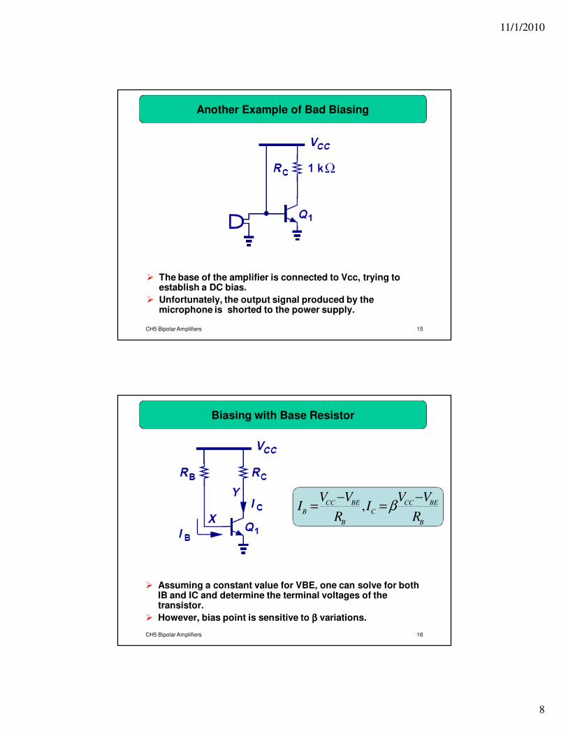
CH5 Bipolar Amplifiers 55
Bad Output Connection
Since the speaker has an inductor, connecting it directly to the amplifier would short the collector at DC and therefore push the transistor into deep saturation.
CH5 Bipolar Amplifiers 56
Still No Gain!!!
In this example, the AC coupling indeed allows correct biasing. However, due to the speaker’s small input impedance, the overall gain drops considerably.

11/1/2010
29
CH5 Bipolar Amplifiers 57
CE Stage with Biasing
OCout
in
OCmv
rRR
RRrR
rRgA
||
||||
)||(
21
=
=
−=
π
CH5 Bipolar Amplifiers 58
CE Stage with Robust Biasing
[ ]
Cout
Ein
E
m
C
v
RR
RRRrR
Rg
RA
=
++=
+
−=
21||||)1(
1
βπ
∞=A
V

11/1/2010
30
CH5 Bipolar Amplifiers 59
Removal of Degeneration for Signals at AC
Capacitor shorts out RE at higher frequencies and removes degeneration.
Cout
in
Cmv
RR
RRrR
RgA
=
=
−=
21 ||||π
CH5 Bipolar Amplifiers 60
Complete CE Stage
43421
4444 34444 21 inThev
Thevout
vv
s
vv
sE
m
LCv
RRR
RR
RRRR
g
RRA
/
21
21
/
21 ||
||
1
||||1
||
+
+++
−=
β
Thevv
21 |||| RRRR sThev =
Thevenin model
of the input

11/1/2010
31
CH5 Bipolar Amplifiers 61
Summary of CE Concepts
CH5 Bipolar Amplifiers 62
Common Base (CB) Amplifier
In common base topology, where the base terminal is biased with a fixed voltage, emitter is fed with a signal, and collector is the output.
11/1/2010
32
CH5 Bipolar Amplifiers 63
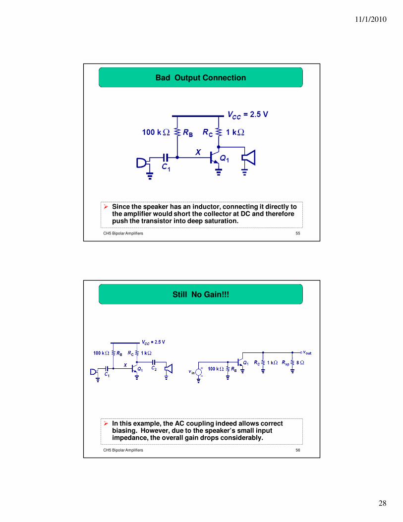
CB Core
The voltage gain of CB stage is gmRC, which is identical to that of CE stage in magnitude and opposite in phase.
CmvRgA =
CH5 Bipolar Amplifiers 64
Tradeoff between Gain and Headroom
To maintain the transistor out of saturation, the maximum voltage drop across RC cannot exceed VCC-VBE.
T
BECC
C
T
C
v
V
VV
RV
IA
−=
= .

11/1/2010
33
CH5 Bipolar Amplifiers 65
Simple CB Example
Ω=
Ω=
==
KR
KR
RgACmv
7.67
3.22
2.17
2
1
CH5 Bipolar Amplifiers 66
Input Impedance of CB
The input impedance of CB stage is much smaller than that of the CE stage.
m
ing
R1
=

11/1/2010
34
CH5 Bipolar Amplifiers 67
Practical Application of CB Stage
To avoid “reflections”, need impedance matching.
CB stage’s low input impedance can be used to create a match with 50 ΩΩΩΩ.
CH5 Bipolar Amplifiers 68
Output Impedance of CB Stage
The output impedance of CB stage is similar to that of CE stage.
COoutRrR ||=

11/1/2010
35
CH5 Bipolar Amplifiers 69
CB Stage with Source Resistance
With an inclusion of a source resistor, the input signal is attenuated before it reaches the emitter of the amplifier; therefore, we see a lower voltage gain.
This is similar to CE stage emitter degeneration; only the phase is reversed.
S
m
C
v
Rg
RA
+
=1
CH5 Bipolar Amplifiers 70
Practical Example of CB Stage
An antenna usually has low output impedance; therefore, a correspondingly low input impedance is required for the following stage.