Fundamentals of Time Interval Measurements - Leap · PDF fileFundamentals of Time Interval...
68
Fundamentals of Time Interval Measurements Application Note 200-3 Electronic Counter Series
Transcript of Fundamentals of Time Interval Measurements - Leap · PDF fileFundamentals of Time Interval...
1
Fundamentals of Time IntervalMeasurements
Application Note 200-3Electronic Counter Series
csamii

2

3
Table of Contents
Precision Time Interval Measurement
Using an Electronic Counter ..................................................... 5
Preface ........................................................................................................... 5
Time Interval Measurement Using an Electronic Counter ........ 6
Introduction .................................................................................................. 6What can be Measured ................................................................................ 6How Measurement is Made ......................................................................... 7
Resolution ...................................................................................... 8
One-Shot Measurements ............................................................................. 8TI Averaging .................................................................................................. 8Minimal Interval, Dead Time and Pulse Width ......................................... 9
Start and Stop Signal Input Channels ....................................... 10
General ........................................................................................................ 10Desirable Characteristics .......................................................................... 10Controls Associated with Time Interval Measurements ....................... 11Input Circuit Operation as it Affects the User ........................................ 11
Input Signal Conditioning Controls and
Trigger Circuit Operation ........................................................ 13
Signal Conditioning Controls Set the Trigger Point............................... 13Other Input Controls .................................................................................. 13Trigger Operation ....................................................................................... 16Determining the Hysteresis Window and Triggering at Zero Volts ..... 24Hysteresis Compensation.......................................................................... 27Polarity Control .......................................................................................... 29Input Attenuators for Measuring Higher Amplitude Signals ................ 30Trigger Lights .............................................................................................. 30Markers ........................................................................................................ 31Delay ! Control ......................................................................................... 34
Time Interval Averaging ............................................................. 36
Reduce +1 or –1 Count Error by N on Repetitive Signals ................ 36Time Interval Averaging is Useful When ................................................. 36Synchronizers Needed for True TI Averaging ........................................ 37Extending Time Interval Measurements to Zero Time.......................... 38Disadvantages of Time Interval Averaging ............................................. 39
Time Interval Error Evaluation ................................................. 40
+1 Count Error or –1 Count Error ........................................................... 40± Trigger Error ........................................................................................... 40± Time Base Error ...................................................................................... 48± Systematic Error ..................................................................................... 49
Time Intervals by Digital Interpolation .................................... 50
Digital Interpolation ................................................................................... 50Phase-Startable Phase-Lockable Oscillators (PSPLO) .......................... 50The Dual Vernier Method .......................................................................... 50
4
The Generation of Precise Time Intervals ................................ 52
Phase-Startable Phase-Lockable Oscillators .......................................... 52
Time Interval Measurement Using the
HP 5363B Time Interval Probes ............................................... 54
Solve Troublesome TI Measurements Problems .................................... 54Level Calibration ......................................................................................... 56Time Zero Calibration ................................................................................. 58To Make a TI Measurement Using the HP 5363B .................................... 59
Some Applications of Time Interval Measurements .................. 60
Simple Timing System with Start-Stop Pulses Generated by Mechanical Switches ............................................................................... 60Phase Measurement .................................................................................... 61Measuring Complex Pulse Trains ............................................................. 63
Comparison with Other Ways of Making Time Interval
Measurements on Narrow Pulses or Fast Rise Signals .......... 67

5
Preface
A time interval measurement is a measurement of the elapsed timebetween some designated START phenomena and a later STOPphenomena. This is in contrast to real-time observations (time of day)used in our day-to-day living to schedule meetings or transportation,in astronomical observations and for celestial navigation among otherthings. One might make a time interval measurement with a mechani-cal stopwatch as when timing a track meet or other sporting event orin making time and motion studies. With increased speed of the timedobject as when timing automobiles or airplanes the timed intervalbecomes shorter and shorter until the human factor involved indetermining when to start and when to stop the measuring device, astopwatch or clock for instance, begins to introduce significant error.Mechanical, optical, or electrical transducers or a combination of allwere developed to reduce this error. Finally with advances in manyscientific fields, mechanical and electrical time measurements wererequired which were beyond the resolution of a mechanical stop-watch. This led to the development of a time interval measuringelectronic counter, in essence an electronic stopwatch. A timeinterval counter can measure electrical delays, pulse widths, andother time related electrical phenomena required in the developmentand maintenance of communications, navigation, television, and otherpresent day systems. Increased measurement capability has helpedbring on more and more sophistication in all of these fields until nowmodern electronic time interval counters are used to measure electri-cal events spaced as close as 0.1 nanosecond (the time required forlight to travel 3 centimeters) on a “one-shot” basis. Time intervalaveraging on repetitive events gives still greater resolution than this.
Precision Time Interval Measurements Using
an Electronic Counter

6
Introduction
Time Interval is an important measurement frequently made withelectronic counters. In this role, the counter makes an elapsed timemeasurement between two electrical pulses, Figure 1, just as a stop-watch is used to time physical events.
Time Interval Measurement Using anElectronic Counter
Figure 1. In a
time interval
measurement,
clock pulses are
accumulated for
the duration the
main gate is
open. The gate is
opened by one
event, START
and closed by the
other, STOP.
Minimum time measurement is much less (to a nanosecond andbelow) than possible with a stopwatch. Also resolution and accuracyare much greater than attainable with a stopwatch.
What Can Be Measured
Some typical time measurements that might be made are:
Characterization of Active Components
Propagation delay of integrated circuitsRadar Ranging
Nuclear and Ballistic Time of Flight
Pulse Measurements
WidthRise TimeRepetition Rate (Period) of pulse trainSpacing on complex pulse trains such as used by airborneidentification and navigation systems
Cable Measurements
Propagation TimeCable Length
Phase
Delay Line Measurements
Time interval measurements can also be made on any physicalphenomena that can be translated into appropriate electrical signals.Transducers such as photo electric cells, magnetic pickups, straingauges, micro-switches, bridge wire systems, or thermistors can beused to translate physical events into the electrical start and stopsignals required for a time interval measurement.
Gate Opens Gate Closes
Start
Stop
Gate
Clock
Accumulated Count
Accumulated Clock Pulses
Open
7
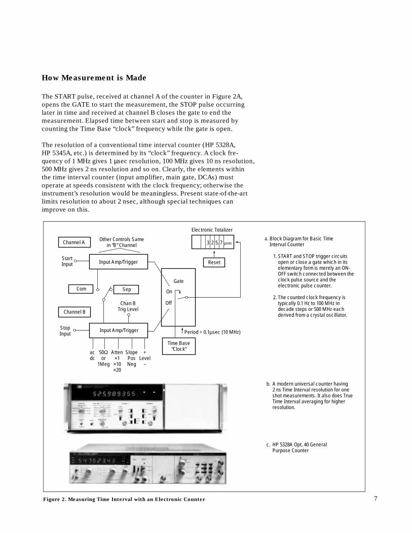
How Measurement is Made
The START pulse, received at channel A of the counter in Figure 2A,opens the GATE to start the measurement, the STOP pulse occurringlater in time and received at channel B closes the gate to end themeasurement. Elapsed time between start and stop is measured bycounting the Time Base “clock” frequency while the gate is open.
The resolution of a conventional time interval counter (HP 5328A,HP 5345A, etc.) is determined by its “clock” frequency. A clock fre-quency of 1 MHz gives 1 µsec resolution, 100 MHz gives 10 ns resolution,500 MHz gives 2 ns resolution and so on. Clearly, the elements withinthe time interval counter (input amplifier, main gate, DCAs) mustoperate at speeds consistent with the clock frequency; otherwise theinstrument’s resolution would be meaningless. Present state-of-the-artlimits resolution to about 2 nsec, although special techniques canimprove on this.
Figure 2. Measuring Time Interval with an Electronic Counter
Channel A
Channel B
Input Amp/Trigger
Input Amp/Trigger
Com Sep
Reset
Time Base "Clock"
Gate
On
Off
3
Start Input
Stop Input
Chan B Trig Level
ac dc
Slope Pos Neg
Period = 0.1µsec (10 MHz)
µsec
Other Controls Same in "B" Channel
+ Level
–
50Ω or
1Meg
Atten ×1 ×10 ×20
2 5. 7
Electronic Totalizer
Block Diagram for Basic Time Interval Counter 1. START and STOP trigger circuits open or close a gate which in its elementary form is merely an ON- OFF switch connected between the clock pulse source and the electronic pulse counter. 2. The counted clock frequency is typically 0.1 Hz to 100 MHz in decade steps or 500 MHz each derived from a crystal oscillator.
a.
A modern universal counter having 2 ns Time Interval resolution for one shot measurements. It also does True Time Interval averaging for higher resolution.
b.
HP 5328A Opt. 40 General Purpose Counter
c.

8
One-shot Measurements
Most general purpose counters will make a “one-shot” (the time be-tween a single pair of start and stop pulses) time interval measurementwith resolution to 100 nanoseconds — i.e., the counter counts a 10 MHzclock. The HP 5328A offers either 100 ns or 10 ns resolution dependingon the configuration. The HP 5345A will resolve a one-shot time intervalmeasurement to 2 nanoseconds. By way of reference 2 nanoseconds isthe time it takes light to travel six tenths of a meter.
For conventional counters, direct readout is achieved by using clockfrequencies related by powers of 10 — i.e., 1 MHz, 10 MHz, 100 MHz,etc., (period of 1 µs, 100 ns, 10 ns, respectively) and a correctly placeddecimal point and annunciator. Single shot resolution of conventionalcounters is limited to 10 ns as the next step up, 1 ns resolution, requiresa 1 GHz direct count decade which at present is not economicallyfeasible. Counters which have arithmetic capability are not limited inthis way as the measurement can be made with any convenient clockperiod then translated to engineering units before being displayed. TheHP 5345A, a reciprocal counter, counts in 2s of nanoseconds then does amultiply by 2 before displaying a time interval measurement. Somesophisticated modern counters like the HP 5370A operate on a digitalinterpolation scheme which allows single shot resolving capability of20 ps. However, with resolution this high other factors like noise in theinput amplifiers or on the input signal become limiting factors. Perhapsa realistic way to look at resolution would be to say it is the probablerepeatability from measurement to measurement for a given set ofcircumstances. Since the two noise components limiting resolution arestatistical in nature the resolution must be described in statistical terms.For example, 30 ps rms would be a typical description of resolutionwhen using the HP 5370A.
TI Averaging
Time interval averaging can be used to get resolution to the picosecond(10–12 sec) region on a repetitive signal. Averaging operates on theassumption that the factors limiting resolution are random in nature andwill tend to average towards zero. A counter needs synchronizers in gatecircuits and a noise modulated clock to achieve TRUE TIME INTERVALAVERAGING with accuracy and repeatability independent of the inputsignal repetition rate. The HP 5345A and HP 5328A with Option 040Universal Module both have this true averaging capability.
Resolution
9
Minimum Interval, Dead Time and Pulse Width
Three important specifications are sometimes overlooked when consid-ering time interval measurements.
1. The minimum time interval or minimum range specification is theminimum time between start and stop pulses which the counter willrecognize. For single shot measurements in a conventional counterthis time must always be one or more clock periods. However, ifinterpolation is used this time can be reduced to in the region of20 ps. A more typical specification is 100 ns corresponding to theperiod of a 10 MHz clock. Another technique for reducing the mini-mum time interval is to use averaging with synchronizers. This allowsintervals of less than one clock period to be measured but a repetitivesignal is required.
2. The minimum dead time is the time from a stop pulse to the accep-tance of the next start pulse. Typical dead time specifications are10 ns for the HP 5345A, 150 ns for the HP 5328A. Dead time deter-mines the maximum upper repetition rate of an acceptable signal.
3. The minimum pulse width is the shortest pulse the counter willrecognize as a start or a stop pulse and is largely determined by thebandwidth of the input amplifiers. The typical minimum pulse widthfor a 50 MHz counter is 10 ns or the period of half a cycle.
Some measurement errors may result if these specifications are notconsidered. For example, if a rise time is being measured which is lessthan the minimum time interval specification the first stop to be recog-nized will be on the next pulse giving a measurement result correspond-ing to the pulse period instead of the desired rise time.

10
General
High resolution is meaningless if measurements on a stable signal arenot repeatable as only the digits that consistently repeat representaccurate information. Since the input amplifier-trigger circuits of thecounter are the interface from the signal of interest to the counter theyare the most critical circuit elements in accurate time interval measure-ments. Their performance directly influences measurement accuracy.Lack of attention to these circuits as related to the measurement is theprime source of measurement error and the major reason a counter’spotential accuracy is often not achieved.
The input amplifier and trigger circuits, one for the start channel and onefor the stop channel, establish the voltage level at which an input signalwill trigger the counter. Noise, drift, ac-dc coupling, and other factorsrelating to these circuits all influence the measurement. Since thesecircuits are so important it is worthwhile looking in some detail at theoperation of one of these input channels.
Desirable Characteristics
Several requirements must be met by each input if a time intervalcounter is to make useful measurements:
1. The input circuits must be able to accept a signal which might be asine wave, square wave, pulse, or a complex waveform of varyingamplitude and generate from that signal one and only one outputpulse of constant amplitude, rise time and width for each cycle of theinput.
2. The circuit will need controls to let the operator choose the exactvoltage point on the input waveform at which he wants to START andSTOP his measurement. This is necessary to achieve flexibility ofmeasurement.
3. The input should have a means of externally setting and/or measuringthe trigger point voltage to facilitate setting up a measurement.
4. The input needs good stability with time and temperature and lowinternal noise so that once set, triggering will occur at the samevoltage level regardless of input signal amplitude, wave shape, orduty cycle.
5. The input should be dc coupled so the trigger voltage point will notchange with repetition rate or duty cycle of the input signal yet becapable of ac coupling for measurements on signals with a dc offset.
Start and Stop Signal Input Channels

11
6. Input circuit protection is necessary so inadvertently applied highamplitude signals, regardless of duration, will not damage inputcircuit components.
7. High input impedance (high input resistance and low input capaci-tance) is desirable for bridging measurements (connecting directlyacross an input signal) with minimum input waveform distortion yetswitchable to 50 ohms to provide a good termination and thus preventreflections when doing fast pulse work in a 50 ohm environment.
8. Provision to connect the start and stop inputs together is desirable tosimplify time interval measurements on a signal appearing on a singlecable. This is necessary for measuring pulse width for instance.
9. Matched input amplifiers are a necessity for meaningful time intervalmeasurements on fast rise time or high frequency signals. If onechannel has significantly less bandwidth than the other, propagationdelay and rise time will be vastly different for the two. This intro-duces large errors in measurements involving high frequency signals.
Controls Associated with Time Interval Measurements
Slope, level and attenuator controls which determine the trigger point onthe input waveform give the operator flexibility in setting up a measure-ment. Understanding the function of each control is important or trigger-ing may not occur at the expected voltage point on the input signal.
Input Circuit Operation as it Affects the User
All electronic counters have an input sensitivity specification, i.e.,100 mV rms for sine waves (282 mV peak-to-peak), which indicates theminimum voltage necessary to operate the counter. This specificationnormally applies over the full environmental range as well as takes intoaccount aging effects, therefore when operated at a moderate roomtemperature, sensitivity may be significantly better than the specifica-tion. Sensitivity may change with aging, with ambient temperature orother environment changes; however, for a well designed circuit theseeffects are held to a minimum. Also sensitivity may depend on frequency.
For frequency measurement, selecting the trigger point is not too critical,the sole requirement being that the counter trigger once (and only once)for each cycle of the input signal. Accurate time interval measurementhowever, places a much more exacting requirement on the input circuitsas they must trigger precisely at the selected trigger voltage set up by theinput controls.
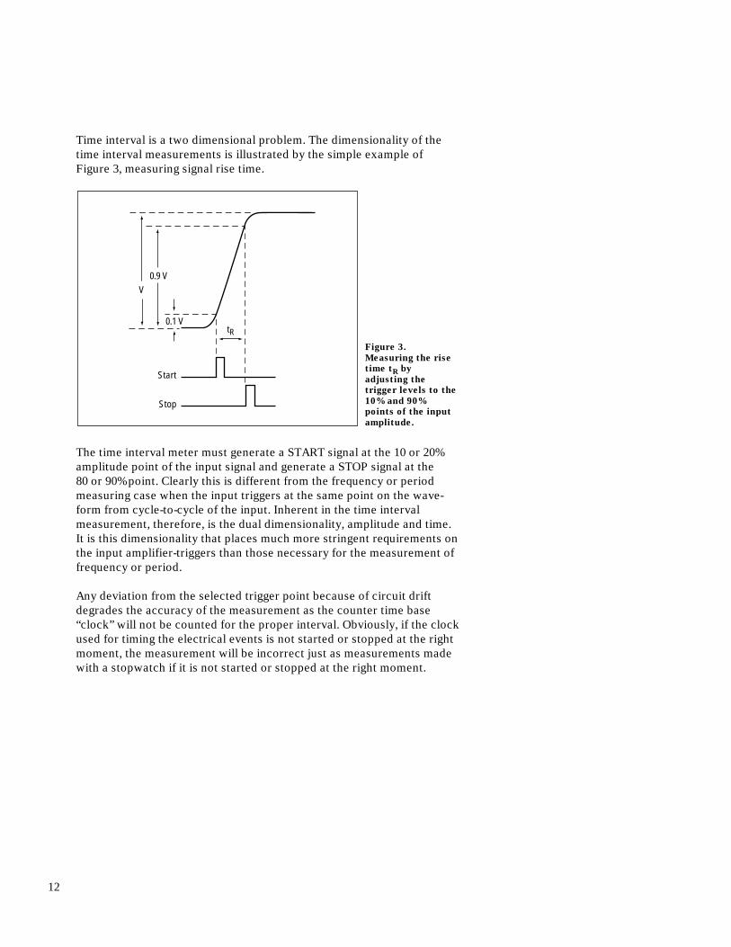
12
Time interval is a two dimensional problem. The dimensionality of thetime interval measurements is illustrated by the simple example ofFigure 3, measuring signal rise time.
The time interval meter must generate a START signal at the 10 or 20%amplitude point of the input signal and generate a STOP signal at the80 or 90% point. Clearly this is different from the frequency or periodmeasuring case when the input triggers at the same point on the wave-form from cycle-to-cycle of the input. Inherent in the time intervalmeasurement, therefore, is the dual dimensionality, amplitude and time.It is this dimensionality that places much more stringent requirements onthe input amplifier-triggers than those necessary for the measurement offrequency or period.
Any deviation from the selected trigger point because of circuit driftdegrades the accuracy of the measurement as the counter time base“clock” will not be counted for the proper interval. Obviously, if the clockused for timing the electrical events is not started or stopped at the rightmoment, the measurement will be incorrect just as measurements madewith a stopwatch if it is not started or stopped at the right moment.
Figure 3.
Measuring the rise
time tR by
adjusting the
trigger levels to the
10% and 90%
points of the input
amplitude.
Stop
Start
V0.9 V
0.1 VtR

13
Signal Conditioning Controls Set the Trigger Point
Figure 4 shows the effects of the SLOPE, POLARITY, LEVEL, andATTENUATOR controls in establishing the trigger voltage point on theinput signal.
1. The SLOPE control determines whether the trigger point will beon a rising or a falling voltage as in Figure 4a.
2. The POLARITY control determines whether the trigger point ispositive or negative with respect to zero volts as in Figure 4b.
3. The LEVEL control adjusts the trigger point of the circuit up ordown in voltage and usually has a range of from one to three voltspeak for a counter with 100 mV rms (282 mV peak-to-peak) sensitiv-ity as in Figure 4c. The polarity and level functions are often com-bined using a zero center variable control having a range of –3 voltsto 0 to +3 volts.
Most counters also have a PRESET switch position at one end of thelevel control range to set up the most sensitive trigger condition forac coupled symmetrical input signals. Functioning of these controlsas they relate to setting a trigger point are discussed in detail later.
4. The INPUT ATTENUATOR reduces high amplitude input signalsup to 100 volts or more so these fall within the dynamic range of theamplifier/trigger circuits which are limited to a few volts rmsmaximum as in Figure 4d.
Other Input Controls
1. SEPARATE COMMON Switch
A SEPARATE common switch ties the START and STOP inputstogether without having to resort to external cables or hardware. Oncounters with 50Ω inputs this is done using appropriate matchingnetworks so the input looks like 50Ω for either the SEPARATE orCOMMON mode of operation. Depending on the circuit configura-tion this may or may not result in a 2:1 loss in voltage sensitivity.
Input Signal Conditioning Controls and
Trigger Circuit Operation

14
2. 50 OHM-HIGH IMPEDANCE Switch
Some modern counters have a panel switch to select a high inputimpedance (1 meg, 35 pF) for bridging applications or 50 ohm inputimpedance to provide a good termination (low VSWR) for a 50 ohmtransmission line. If the counter has a 50Ω position the whole inputcircuit up to the gate of Q1 (Figure 6) is designed as a 50 ohm stripline. Also, the overload protection resistor R1 is shorted out so theoperator must be more careful when measuring high amplitudeinput signals (usually 5V rms maximum) or the input circuit can bedamaged.
3. dc-ac Coupling
All general purpose time interval counters have a dc coupledamplifier trigger circuit so as to maintain a consistent trigger pointon input signals down to zero frequency. AC coupling, when needed,is achieved by connecting a capacitor, C1, in series with the inputconnector either with a switch or through a second input connector.AC coupling is necessary when measuring a signal with a large dcoffset; however, the trigger point changes with both the inputfrequency and duty cycle when using ac coupling.
4. CHECK
While not strictly related to time interval measurements, the SELFCHECK function checks the multiplier, divider, and gate circuits of acounter for correct operation and should be done before using acounter. The self check function does not give any indication ofcrystal oscillator accuracy.

15
Figure 4. The three parameters under operator control which define the trigger point on an input signal.
A. Slope
B. Polarity
C. Level
D. Attenuator
Voltage to input amplifier
+
0
+
00
0
+3
–3
+100
+10
+10
–1
–10
–100
– Overload
+ Overload
–TRIGGER ON POSITIVE SLOPE • Rising voltage • Independent of polarity
TRIGGERING ON PLUS POLARITY • Triggers at some voltage above zero
TRIGGERING ON NEGATIVE POLARITY • Trigger at some voltage below zero
TRIGGER ON NEGATIVE SLOPE • Falling voltage • Independent of polarity
Volts
Inpu
t Vol
ts
×100
×10
×1
+
0
–
–
• Triggering can be set to occur at any level within the dynamic range of the input circuit

16
Trigger Operation
The input amplifier trigger circuit accepts the input signal which mayvary in amplitude, frequency, and wave shape. It puts out one pulse ofconstant amplitude and width as required by the internal countercircuits each time the input signal crosses the selected trigger voltagepoint.
1. HYSTERESIS LIMITS define input sensitivity
The input signal must cross two voltage thresholds to activate thetrigger circuit. The sensitivity of the electronic counter is deter-mined by the voltage difference between these two thresholds,called hysteresis limits, which define the hysteresis window of thetrigger circuit. The hysteresis limits correspond to voltage levels onthe input signal, one of which will trigger the circuit Figure 5a, at(m) and the other voltage level which will reset the trigger circuit at(n). A plot, Figure 5b, of the transfer function of the trigger output
Positive Slope
Inpu
t Vol
ts
+0.3
+0.2
+0.1
0
m
n–0.1
–0.2
–0.3
VU
VC
VL
V2
V1
V2
V1
Input Signal
Trigger
Hysteresis window defined by upper hysteresis limit VU and lower hysteresis limit VL.
Triggering on positive slope Triggering on negative slope
Output Voltage
Reset Trigger Circuit
Output Pulse from Trigger Circuit
a.
–0.2 –0.1 0 +0.1 +0.2
Triggering on a positive slope. Signal must cross both hysteresis limits to activate the trigger circuit.
b. A plot of the transfer function of the input trigger circuit of an electronic counter resembles the BH curve of a magnetic core.
Outp
ut V
olts
Lower Hysteresis Unit Upper Hysteresis Unit
Hysteresis Window
Figure 5. Hysteresis limits and transfer function of a trigger circuit.
17
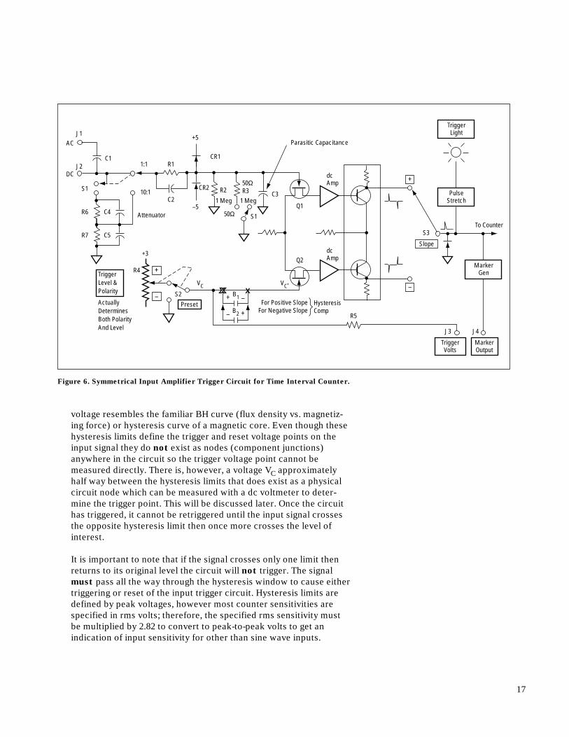
voltage resembles the familiar BH curve (flux density vs. magnetiz-ing force) or hysteresis curve of a magnetic core. Even though thesehysteresis limits define the trigger and reset voltage points on theinput signal they do not exist as nodes (component junctions)anywhere in the circuit so the trigger voltage point cannot bemeasured directly. There is, however, a voltage VC approximatelyhalf way between the hysteresis limits that does exist as a physicalcircuit node which can be measured with a dc voltmeter to deter-mine the trigger point. This will be discussed later. Once the circuithas triggered, it cannot be retriggered until the input signal crossesthe opposite hysteresis limit then once more crosses the level ofinterest.
It is important to note that if the signal crosses only one limit thenreturns to its original level the circuit will not trigger. The signalmust pass all the way through the hysteresis window to cause eithertriggering or reset of the input trigger circuit. Hysteresis limits aredefined by peak voltages, however most counter sensitivities arespecified in rms volts; therefore, the specified rms sensitivity mustbe multiplied by 2.82 to convert to peak-to-peak volts to get anindication of input sensitivity for other than sine wave inputs.
Figure 6. Symmetrical Input Amplifier Trigger Circuit for Time Interval Counter.
X
J1AC
J2C1
1:1
10:1
R1
C2
Attenuator
+5
CR1
CR2 R2
1 Meg 1 Meg
50Ω R3
–550Ω S1
C3
Q1
Q2
dc Amp
dc Amp
DC
S1
R6
R7
C4
C5
+3
R4
S2
R5
S3
J4J3
To Counter
VC VC'B1
B2
Preset
+
–
+
–
Trigger Level & Polarity
Actually Determines Both Polarity And Level
For Positive Slope For Negative Slope
Hysteresis Comp
Slope
Pulse Stretch
Trigger Light
Marker Gen
Marker Output
Trigger Volts
Parasitic Capacitance
+
+
–
–

18
This triggering action might be compared to a mouse trap. With thetrap, nothing happens until the trigger is depressed below a certainpoint at which time the trap is sprung. Operation of the trap oncetripped is independent of how fast or how slow the trigger wasdepressed. Once sprung, further movement of the trigger has noeffect until the trap is reset. Triggering the trap corresponds tocrossing the upper hysteresis limit (m) of Figure 5a, resetting thetrap corresponds to crossing the lower limit (n) for this example.
2. TRIGGER CONTROLS as they relate to the input circuit
The diagram, Figure 6 of a typical input amplifier for one channel ofa solid state time interval counter shows the circuit elements whichare directly influenced by the setting of panel controls. A look at thecircuits associated with each control helps understand the correctsetting procedure needed to make valid time interval measurements.
a. Input Attenuator
The frequency compensated input attenuator, R6R7C1C5, reducesan input level up to 100 volts or more by a factor of 100:1, 20:1,10:1, or 2:1 (sometimes labeled x100, x20, x10, x2) to a level thatcan be safely applied to the input amplifier circuit. One usuallythinks of an attenuator as a device that reduces the input signalto the linear range of the input amplifier. With respect to thesignal, another way to look at attenuator operation is that itmultiplies the hysteresis window of the counter by the attenua-tion factor. For example, the counter with a 25 mV rms sensitivity(hysteresis limits 25 × 2.82 = 70.5 millivolts apart) would have250 mV rms sensitivity (hysteresis limits 25 × 2.82 × 10 = 705millivolts apart) on the X10 attenuator setting. Even though largesignals applied to a sensitive range may not damage the counterthe overload may cause miscounting.
b. Overload Protection
Diodes CR1 and CR2 in conjunction with R1 provide overloadprotection to prevent damage to Q1 in case of accidental over-load. R1 is large enough to prevent damage with an input signalas high as 115 volts rms at power line frequency on the mostsensitive attenuator range of most counters. A capacitor, C2,across this resistor prevents sensitivity roll off at high frequen-cies. Important to the operator is the fact that at high frequen-cies, C2 effectively shorts out the protection resistor R1 somaximum voltage is limited to a few volts rms, Figure 7, ratherthan 100 volts or more as at low frequencies.

19
Also important to the operator is the fact that the protectivediodes CR1 and CR2 can change the input characteristics of thecounter. So long as the input signal is below ±5 volts peak thediodes CR1 and CR2 for the circuit in Figure 5 are back biased sohave no effect. If the peak input signal goes beyond these limitshowever, the input resistance of the counter drops from1 megohm down to a value perhaps as low as a few hundredohms dependent on the value of R1. This places a heavy non-linear load on the signal source which may drastically alter itswaveshape. For normal operation the input signal must be keptbelow this overload level even though the input circuit may notbe damaged because double counting or other erratic countingmay occur due to the shape of the altered input signal. Whenworking with a transducer such as a tachometer generator whichhas an output proportional to rotational speed, the simpleexternal limiter shown in Figure 8 is effective in preventingcounter overload for a signal that varies over wide amplitudelimits. When using this circuit, the source always sees a minimumload of 22K at the input to the limiter so ringing and otherdistortion is not a problem. When working with low frequencysources (below 50 kHz) such as tachometer and flowmeterpickups C1, in the range of 100 to 500 pF, keeps high frequencynoise from causing false triggering. The input signal is symmetri-cally clipped as amplitude increases so the trigger point of thecounter must be set between ±0.5 volts.
Figure 7. Overload
voltage as a
function of
frequency.
Volts
Pea
k
150
5
60 Hz 1000 HzFreq
Figure 8. Simple
clipper circuit to
prevent counter
input overload.
Input From
Transducer
Output To Counter High Impedance Input
R1 22K
C1 500pF CR1 CR2
Diodes 1N914 Silicon Diodes or 1901-0040
20
c. dc or ac Coupling
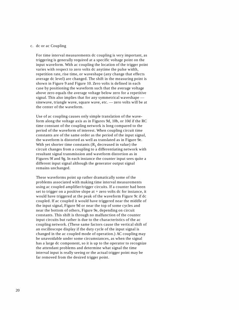
For time interval measurements dc coupling is very important, astriggering is generally required at a specific voltage point on theinput waveform. With ac coupling the location of the trigger pointvaries with respect to zero volts dc anytime the pulse width,repetition rate, rise time, or waveshape (any change that effectsaverage dc level) are changed. The shift in the measuring point isshown in Figure 9 and Figure 10. Zero volts is defined in eachcase by positioning the waveform such that the average voltageabove zero equals the average voltage below zero for a repetitivesignal. This also implies that for any symmetrical waveshape —sinewave, triangle wave, square wave, etc. — zero volts will be atthe center of the waveform.
Use of ac coupling causes only simple translation of the wave-form along the voltage axis as in Figures 9d, 10b, or 10d if the RCtime constant of the coupling network is long compared to theperiod of the waveform of interest. When coupling circuit timeconstants are of the same order as the period of the input signal,the waveform is distorted as well as translated as in Figure 9e.With yet shorter time constants (R1 decreased in value) thecircuit changes from a coupling to a differentiating network withresultant signal transmission and waveform distortion as inFigures 9f and 9g. In each instance the counter input sees quite adifferent input signal although the generator output signalremains unchanged.
These waveforms point up rather dramatically some of theproblems associated with making time interval measurementsusing ac coupled amplifier/trigger circuits. If a counter had beenset to trigger on a positive slope at + zero volts dc for instance, itwould have triggered at the peak of the waveform Figure 9c if dccoupled. If ac coupled it would have triggered near the middle ofthe input signal, Figure 9d or near the top of some cycles andnear the bottom of others, Figure 9e, depending on circuitconstants. This shift is through no malfunction of the counterinput circuits but rather is due to the characteristics of the accoupling network. (These same factors cause the vertical shift ofan oscilloscope display if the duty cycle of the input signal ischanged in the ac coupled mode of operation.) AC coupling maybe unavoidable under some circumstances, as when the signalhas a large dc component, so it is up to the operator to recognizethe attendant problems and determine what signal the timeinterval input is really seeing or the actual trigger point may befar removed from the desired trigger point.

21
Figure 9. dc and ac Coupling for a complex pulse train.
Coupling
b. Coupling Network
Input Output
ac
dc
R1C1 0.033 µf
+1V
0V
–1V
+1V
0V
–1V
+1V
0V
–1V
a. Input Signal
c. dc Coupling Output Signal
c. dc Coupling Output Signal (Same as "c" above.)
d. ac Coupling R1 = 1 Meg Time constant of the coupling network is long compared to the period of the input signal. Note: The output waveform is preserved but the dc level has shifted.
e. ac Coupling R1 = 47K Time constant of the coupling network is about the same as the period of the input signal. Note: The output waveform is distorted and the dc level has shifted.
f. ac Coupling R1 = 10K Time constant of the coupling network is shorter than 5 milliseconds. Note: The output waveform differentiated only with respect to the low frequency component of the input signal.
g. ac Coupling R1 = 2200 ohms Time constant of the coupling network is much shorter than the shortest period of the input signal. Note: The output waveform is completely differentiated, i.e., the output voltage returns to zero after each input transition.
22
Figure 10. dc or ac Coupling illustrating change in Zero Level with Pulse Width.
+1V
0V
–1V
+1V
0V
–1V
a. dc Coupling b. ac Coupling C1 = 0.033 µF, R1 = 47K
Time constant of the coupling network is long compared to the period of the input signal. Note: Average voltage of the input signal is near zero so dc shift is small.
c. dc Coupling d. ac Coupling C1 = 0.033 µF, R1 = 47K Same coupling network as for waveform above. Note: Average voltage of the input signal is approximately –1 volt so dc shift is large when switching to ac coupling.
AC COUPLING CIRCUIT IS THE SAME AS FOR FIGURE 9.
d. Slope Control
The slope control, S3 Figure 6, determines if the circuit is trig-gered by a signal with a positive (+) slope (going from onevoltage to a more positive voltage regardless of absolute polarity)to generate an output pulse at the upper hysteresis limit (VU) ofFigure 5a, or by a signal with a negative (–) slope which causes anoutput pulse to be generated at the lower hysteresis limit (VL).
e. Level Control
Moves hysteresis window voltage-wise. The level control, R4Figure 6 moves the center of the hysteresis window VC to anypositive or negative voltage within the dynamic range of the input

23
circuit without appreciably changing the window as in Figure 11.Best sensitivity for an ac coupled, sine wave input signal is withthe hysteresis limits positioned symmetrically with respect to0 volts dc since the smallest amplitude signal can now cross bothlimits. Many counters have a PRESET position at one end of therange of the LEVEL control to set up this condition. (Triggeringwill occur at either the upper or lower hysteresis limit dependingon the setting on the SLOPE control.)
The voltage VC which defines the approximate center of thehysteresis limits comes from the arm of the TRIGGER LEVELcontrol, R4, Figure 6, so can be measured with a dc voltmeter.This voltage is often brought to a panel connector, J3, for ease ofmeasurement. A resistor, R5, of several thousand ohms may beincluded to prevent circuit damage if J3 is accidentally shorted;therefore, a high impedance voltmeter should be used.
f. Triggering at a Particular Voltage
To actually trigger at a particular voltage, either the upperhysteresis limit, VU, or lower hysteresis limit VL, (once againdepending on slope) must be positioned at the desired voltagelevel using the LEVEL control. This is not easy since VU or VLcannot be measured with a voltmeter as mentioned earlier.Instead, one must measure the hysteresis window peak-to-peakvoltage, Figure 12, then add 1/2 this value to VC when triggering ona positive slope or subtract when triggering on a negative slope todetermine the actual trigger point.
V VV V
V VV V
Trigger CU L
Trigger CU L
= +
= +
–
–2
2
for positive slope
for negative slope
Where: VC can be measured with a dc voltmeter.
The hyteresis window, VU–VL, can be determinedusing procedures outlined in the following section.
Figure 11. Polarity
and Level Controls
0.5
+
–
0.40.3
0.2
0.10.20.3
0.4
0.5
0.10
Peak
Vol
ts
Hysteresis Window
VU
VCVL
VUVCVL
VUVC
VL

24
Determining the Hysteresis Window and Triggering
at Zero Volts
The distance between the hysteresis limits VU–VL (hysteresis window)which defines input sensitivity can be determined using one of thesemethods:
1. Methods of Measuring of Hysteresis Window and Determining VC
a. The first method, Figure 13a, measures the hysteresis window bycounting a low distortion 10 kHz to 100 kHz sine wave input tothe counter. Reduce the input amplitude, readjust the triggerLEVEL control, then repeat these steps to determine the mini-mum amplitude signal that will just trigger the counter. Thehysteresis limits are then spaced by the peak-to-peak sine wavevoltage. This is 2.82 × rms input voltage measured with an acvoltmeter. A calibrated dc coupled oscilloscope and a sine waveor a square wave generator could also be used in a similarmanner. In this case, the × 2.82 factor is not needed since anoscilloscope already displays peak-to peak volts.
b. The second method, Figure 13b, is the inverse of the first methodin that the hysteresis limit of interest is moved through a zerovolt input signal to establish triggering at zero volts. For trigger-ing on a positive slope, the counter input is first groundedinsuring zero volts input, then the trigger LEVEL control isturned to its most positive extreme after which it is decreasedslowly until the input circuit just triggers. Triggering occurs whenthe upper hysteresis limit coincides with the input voltage whichis zero because of the grounded input terminal. Voltage
′−
VV V
CU L,
2 and negative in this case, can be measured at J3
with a dc voltmeter. This voltage which is one-half the hysteresiswindow is added to other VC settings to get the actual triggervoltage for any settings within the linear range of the LEVELcontrol. The same can be done when triggering on a negativeslope except the trigger LEVEL control is first turned to its mostnegative extreme then slowly advanced until the circuit justtriggers. The measured difference voltage is subtracted from
Figure 12. To
trigger at a
particular voltage
(zero volts dc in
this example) with
a positive slope.
Upper and lower
hysteresis limits
are positioned as
shown above.
Trigger PointPositive Slope
Hysteresis WindowVU0
0.10.2
+
Volts
0.20.1 VC
VL
Hysteresis Limits
–

25
other VC readings to get the actual trigger voltage.
c. A third method of determining V VU L−
2, Figure 13c, requires a
square wave generator with a variable output amplitude thatswings between some minus voltage and zero or between zeroand some plus voltage. Zero volts must be accurately at 0 as anyresidual offset will give incorrect results. For triggering on thepositive slope, turn the LEVEL control on the counter to its mostpositive extreme. Connect a 10 kHz square wave that goes from–1 volt to 0 to the input of the counter. Slowly decrease thetrigger LEVEL until the counter just begins to trigger. Thishappens when the upper hysteresis limit coincides with upperexcursion (0 volts) of the input square wave. Triggering is at zerovolts and V'C can be measured as before.A similar procedure can be used to establish triggering at zero
Figure 13.
Determining the
hysteresis window,
i.e., spacing
between the
hysteresis limits,
which define the
sensitivity of an
electronic counter
and setting trigger
levels at zero
volts.
+
–
0
Volts
Hysteresis Window
Hysteresis Window
Hysteresis Limits
Can be measured with a dc voltmeter
VU
VU
VC
VL
V'U V'U – V'LV'CV'L
VL
VC
a. Using sine wave or square wave to determine spacing between hysteresis limits.
b. With input grounded, hysteresis limits are moved slowly downward with TRIGGER LEVEL control until input circuit triggers once. V'C can be measured.
Triggering ceases if input signal does not touch or cross both upper and lower hyteresis limits.
For positive slope Circuit triggers when the upper hysteresis limit crosses zero volts
+
–
0
Inpu
t Gro
unde
d
VU
VL
c. With square wave input 0 to –1 volt triggering begins when upper hysteresis limits coincide with top of square wave at zero volts.
+
–
0
Hysteresis WindowNo Triggering
V'UV'CV'L
Begins triggering for positive slope
2=
26
volts with a negative slope. In this case, the square wave outputis from +1V to 0 volts and the LEVEL control is initially offset toits negative extreme.
2. Establishing Triggering at Zero Volts on a Sine Wave
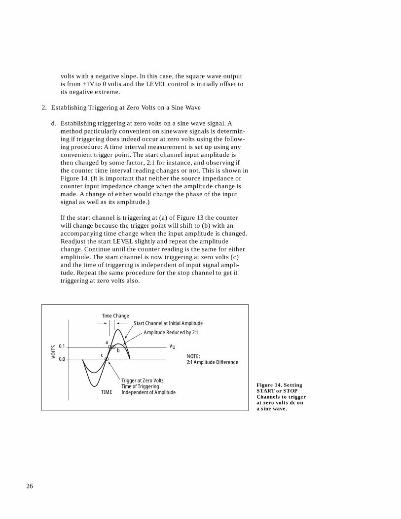
d. Establishing triggering at zero volts on a sine wave signal. Amethod particularly convenient on sinewave signals is determin-ing if triggering does indeed occur at zero volts using the follow-ing procedure: A time interval measurement is set up using anyconvenient trigger point. The start channel input amplitude isthen changed by some factor, 2:1 for instance, and observing ifthe counter time interval reading changes or not. This is shown inFigure 14. (It is important that neither the source impedance orcounter input impedance change when the amplitude change ismade. A change of either would change the phase of the inputsignal as well as its amplitude.)
If the start channel is triggering at (a) of Figure 13 the counterwill change because the trigger point will shift to (b) with anaccompanying time change when the input amplitude is changed.Readjust the start LEVEL slightly and repeat the amplitudechange. Continue until the counter reading is the same for eitheramplitude. The start channel is now triggering at zero volts (c)and the time of triggering is independent of input signal ampli-tude. Repeat the same procedure for the stop channel to get ittriggering at zero volts also.
Figure 14. Setting
START or STOP
Channels to trigger
at zero volts dc on
a sine wave.
Time Change
Trigger at Zero Volts Time of Triggering Independent of AmplitudeTIME
Start Channel at Initial Amplitude
Amplitude Reduced by 2:1
0.1
0.0VOLT
S VU
NOTE: 2:1 Amplitude Difference
ab
c
27
Hysteresis Compensation
1. What is Hysteresis Compensation?
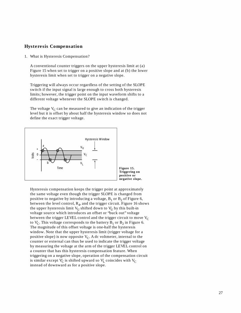
A conventional counter triggers on the upper hysteresis limit at (a)Figure 15 when set to trigger on a positive slope and at (b) the lowerhysteresis limit when set to trigger on a negative slope.
Triggering will always occur regardless of the setting of the SLOPEswitch if the input signal is large enough to cross both hysteresislimits; however, the trigger point on the input waveform shifts to adifferent voltage whenever the SLOPE switch is changed.
The voltage VC can be measured to give an indication of the triggerlevel but it is offset by about half the hysteresis window so does notdefine the exact trigger voltage.
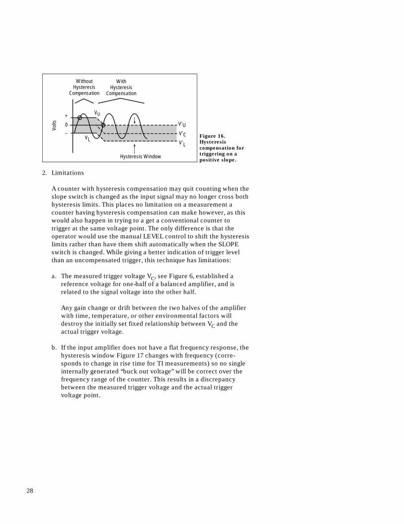
Hysteresis compensation keeps the trigger point at approximatelythe same voltage even though the trigger SLOPE is changed frompositive to negative by introducing a voltage, B1 or B2 of Figure 6,between the level control, R4, and the trigger circuit. Figure 16 showsthe upper hysteresis limit VU shifted down to V'U by this built-involtage source which introduces an offset or “buck out” voltagebetween the trigger LEVEL control and the trigger circuit to move VCto V'C. This voltage corresponds to the battery B1 or B2 in Figure 6.The magnitude of this offset voltage is one-half the hysteresiswindow. Note that the upper hysteresis limit (trigger voltage for apositive slope) is now opposite VC. A dc voltmeter, internal to thecounter or external can thus be used to indicate the trigger voltageby measuring the voltage at the arm of the trigger LEVEL control ona counter that has this hysteresis compensation feature. Whentriggering on a negative slope, operation of the compensation circuitis similar except V'C is shifted upward so V'L coincides with VCinstead of downward as for a positive slope.
Figure 15.
Triggering on
positive or
negative slope.
VU
VC
VL
Hysteresis Window
Time
Volts 0
+
–
a
b
28
2. Limitations
A counter with hysteresis compensation may quit counting when theslope switch is changed as the input signal may no longer cross bothhysteresis limits. This places no limitation on a measurement acounter having hysteresis compensation can make however, as thiswould also happen in trying to a get a conventional counter totrigger at the same voltage point. The only difference is that theoperator would use the manual LEVEL control to shift the hysteresislimits rather than have them shift automatically when the SLOPEswitch is changed. While giving a better indication of trigger levelthan an uncompensated trigger, this technique has limitations:
a. The measured trigger voltage VC, see Figure 6, established areference voltage for one-half of a balanced amplifier, and isrelated to the signal voltage into the other half.
Any gain change or drift between the two halves of the amplifierwith time, temperature, or other environmental factors willdestroy the initially set fixed relationship between VC and theactual trigger voltage.
b. If the input amplifier does not have a flat frequency response, thehysteresis window Figure 17 changes with frequency (corre-sponds to change in rise time for TI measurements) so no singleinternally generated “buck out voltage” will be correct over thefrequency range of the counter. This results in a discrepancybetween the measured trigger voltage and the actual triggervoltage point.
Figure 16.
Hysteresis
compensation for
triggering on a
positive slope.
V'U
VU
V'CV'L
VL
Hysteresis Window
Volts 0
+
–
Without Hysteresis
Compensation
With Hysteresis
Compensation

29
3. HP 5328A Option 040 and HP 5326A/B, 5327A/B have HysteresisCompensation
The HP 5328A Option 040 and the HP 5326A/B and HP 5327A/Bcounters have this hysteresis compensation feature in the timeinterval mode of operation. An HP 5328A with Option 040 (timeinterval) and Option 020 or 021 (digital voltmeter) has switch posi-tions labeled READ A and READ B to select and display either InputA (start) or Input B (stop) trigger voltage to 1 millivolt. One millivoltresolution is greater than justified in terms of absolute accuracy ofthe trigger voltage for reasons mentioned earlier; however, this highresolution is useful as it is possible to:
a. Return very closely to a previously selected trigger voltage.
b. Accurately move the trigger point by some small amount sincethe DVM gives 1 millivolt resolution on ∆V readings. This ishelpful when determining rise times.
The HP 5326B or HP 5327B which has a built-in DVM also has aREAD LEVEL A and READ LEVEL B position to read trigger voltagein the time interval mode.
Polarity Control
This control determines if the center of the hysteresis window moves toa positive voltage or to a negative voltage from zero when the levelcontrol is changed. Most counters have the level control connectedbetween a +V and a –V supply. This puts 0 volts in the center of thecontrol range so a single control functions both as a POLARITY and aLEVEL control as in Figure 6. In this case the control element may havea nonlinear taper to give greater settability around zero volts. Thevoltage from the arm of the level control to the trigger circuit is oftenbrought to an external connector where it can be measured with a dcvoltmeter. This voltage defines the approximate center of the hysteresiswindow, VC.
Figure 17.
Hysteresis
window gets
wider if input
sensitivity
decreases with
increasing
frequency.
Hysteresis Window
Input Frequency
Max
Inpu
t Vol
ts
+0.4
+0.2
0.0
–0.2
–0.4
0
VU
VL
30
Input Attenuator for Measuring Higher
Amplitude Signals
A frequency compensated 2:1, 10:1, 20:1, or 100:1 attenuator betweenthe input terminal and the input amplifier permits measurement of highamplitude signals which might otherwise overload or damage the inputcircuit. This attenuator has the effect of increasing the hysteresiswindow by the attenuation factor, for instance: a counter with 100 mVrms sensitivity would have a hysteresis window of 282 millivolts (peak-to-peak value of 100 mV rms). The x10 position on the attenuationraises sensitivity to 1V rms and the hysteresis window becomes 2.82volts so signals below this amplitude can no longer be counted. Similarreasoning applies for other attenuation factors.
The SLOPE, POLARITY, LEVEL, and ATTENUATOR controls allow theoperator to start or stop a measurement anywhere on an electricalinput signal except the most negative part of the signal when triggeringon a positive slope or the most positive part of a waveform whentriggering on a negative slope. (At the peak, one or the other of thehysteresis limits is no longer crossed by the signal.) Operation of thesecontrols is similar to that on the sweep circuit of a modern oscillo-scope. On the oscilloscope these controls determine where, on an inputwaveform, the sweep begins. On the counter they determine where onthe signal the measurement begins and ends.
Trigger Lights
When measuring time interval the counter displays a reading only if itgets a Start and a Stop pulse. During setup on an unknown signal it isnot always obvious if both input channels are triggering or not if thecounter is not gating. To make initial setup easier, trigger lights, one foreach channel, are often provided. A neon lamp or LED is used toindicate channel activity so the operator can tell by looking at the lightif the channel in question is triggering regardless of whether the other istriggering or not. The trigger light drive circuit includes a pulsestretcher to insure that the light stays on long enough to be seen eventhough the actual input pulse may be too narrow.
1. Two-State
Two general types of trigger light presentations are used: The twostate display used on the HP 5308A and on the HP 5326/5327 seriescounters has lights that are OFF when the circuit is not triggeringbut BLINK when the circuit is triggering. As the input repetition rateincreases above about 50 Hz the trigger lights appear to stay oncontinuously.

31
2. Three-State
The trigger lights of the three state display used on the HP 5328Amay be OFF, BLINKING, or ON. A trigger light is OFF if the input isbelow the trigger level (due to too small a signal, a dc component onthe signal or the trigger level control incorrectly set) and ON continu-ously (but no triggering) when the input is above the trigger level.The light BLINKS each time the input triggers for rates up to about10 Hz and blinks at about a 10 Hz rate for inputs of 10 Hz to 100 MHz.This not only gives the operator an indication of triggering but alsosome indication of the problem if the counter is not triggering.
Markers
Many electronic counters generate electrical signals for use as markerswhen an input channel is triggered.
Some types of markers are:
1. DOT MARKERS
When a channel is triggered it puts out a short duration electricalmarker pulse (100 ns wide) that can be used to intensity modulatethe trace of an oscilloscope displaying the input signal. The markershows up on an oscilloscope display as a bright dot on the waveform.
Dot marker pulses, Figure 18a, are useful to indicate the trigger pointon a slow rise waveform since marker width and circuit delays areboth small compared to the risetime of the input waveform; how-ever, as one gets into fast risetime pulses these effects are no longerinsignificant. This coupled with the CRT phosphor rise and decaytime makes intensity markers of little use in the nanosecond regionas the markers begin to look more like comets than dots so theactual trigger point is no longer well defined.
Dot marker outputs are useful on sine wave signals from 100 Hz to100 kHz. At higher frequency, the marker width becomes an appre-ciable part of the period of the input signal so the marker no longerdefines a specific point on the input waveform. Also the delaythrough the intensity modulation (Z axis) amplifier is not usuallyknown so dot markers are of little use in the sub-microsecondregion.
At low frequencies, dot markers are not useful unless the dot widthis increased as the trace is intensified for such a small portion ofone cycle that it is difficult to see the marker. Separate connectorsare supplied for the START marker and STOP marker outputs onmost time interval counters.

32
2. GATE MARKERS
A gate marker, Figure 18b, generates a dc voltage for the duration ofthe counter measurement (gate OPEN to gate CLOSE). This can beused to intensify an oscilloscope display of the input signal from thereceipt of a START signal by the counter until the receipt of a STOPsignal.
High impedance gate markers work well to very low frequencies orto demonstrate basic triggering ideas on time interval measurementsbut are not useful for fast pulse or short delay measurements as theyhave the same drawbacks as dot markers. Figure 19 shows markersas they appear on an oscilloscope.
NOTE: Dot markers come from the trigger circuit so they appearon every input cycle. A gate marker appears only when thegate is open so it does not appear unless the gate opens.
Figure 18. Time
Interval Markers
as they appear on
an oscilloscope.
Figure 19. Actual
Dot and Gate
Marker Outputs
0
+1
–1
0
+1
–1
Start Positive Slope Triggers at +0.7 Volts
Stop Negative Slope –0.5 Volts
TI Measured
Peak
Vol
ts
+2
–2
a. DOT Markers. Both the stop and the start markers have been connected to the Z axis (intensity modulation) input of an oscilloscope.
b. GATE marker for the same measurement as in (a).
TI
+2V0V
–2V0V
0V
0V
0.5ms
HP 5326A/B — HP 5327A/B Marker and Gate Outputs
Start (A Channel) marker triggering on positive slope at +1.25 voltsStop (B Channel) marker triggering on negative slope at –1.25 volts
Combined markers
Gate output for above conditions

33
Figure 20.
HP 5328A Gate
Output 1 peak-to-
peak into 50 ohm
load.
1 ms
Input Signal
Gate Output 1V P-P
Marker Output
The HP 5345A and HP 5328A Option 040 also have 50Ω gate outputs.These have fast risetime. They are useful over the full frequencyrange of the counter as this gate output can be displayed on thesecond channel of a wide band oscilloscope connected to the signalor can be mixed with the input signal before display. These gatemarkers may be offset from the actual gate time by 10 ns to 100 ns.For detailed information consult the data sheet for a specificcounter. Figure 20 and Figure 21 are illustrations of markers.
3. SQUARE WAVE MARKERS
The HP 5328A has 100 mV into 50 ohm marker outputs which areinverted replicas of the Channel A and Channel B Schmitt triggeroutputs as in Figure 21b. These can be displayed along with the inputsignal on a dual channel oscilloscope. These markers are fast enoughthat they are useful to 100 MHz in a 50Ω system. In general there issome delay between the marker output and actual triggering so thecounter data sheet should be consulted for detailed information. TheHP 5328A Option 040 High Performance Universal Module has aChannel A marker as described above as well as a gate type markerwhich is high during a TI A B measurement. Both are available fromfront panel connectors.
34
Figure 21.
Square wave
marker output
of the HP 5328A
Counter.
Delay ! Control
Besides the conventional input controls, the HP 5328A Option 040 andthe HP 5304A each have a DELAY control associated with the startinput. This control is useful in making a measurement on a complex ornoisy signal. Once a measurement begins (following a START pulse)STOP pulses are locked out until expiration of a pre-determined,adjustable, analog delay. The measurement terminates with the firstSTOP pulse following delay run down. This feature is useful in relaytesting for example as the delay is used to get away from errors due tocontact bounce. In Figure 22a, a measurement started at 1 wouldnormally end at 2 on the first bounce. Adjusting the delay time tosomething greater than 3 but less than 4 lets the operator measure thetime from the first contact closure to the first contact opening after thecoil is de-energized. Figure 22b illustrates another application where ameasurement is required between specific pulses on a complex pulse
(B)
1µs
1µs
(A)
+1V0V
–1V
+1V
a. HP 5328A Standard Unit Marker Output into 50 Ohm Load. Positive Slope - Triggers at Trailing Edge of Marker at (A). Negative Slope - Triggers at Leading Edge of Marker (B).
b. HP 5328A Option 040 Marker Output into 50 Ohm Load. Triggering always corresponds to Leading Edge of Marker.
0V–1V
Input Signal
Triggering at 0 voltsTriggering at –1.25 volts Marker OutputTriggering at +1.25 volts
Input Signal
Triggering, Positive Slope, 0 volts
Triggering, Negative Slope, 0 voltsTriggering, Positive Slope, +1.25 voltsTriggering, Positive Slope, –1.25 volts

35
train such as that used in ATC (Air Traffic Control) systems for ex-ample. Here the DELAY control is used to select specific STOP locationswithin the pulse train. The SAMPLE RATE control is also helpful as thisgives control of the counter “dead time” and so gives some control ofthe time between pulse trains.
The HP 5345A can also be used for this kind of measurement; however,in this case the DELAY signal is generated by an external generator suchas the HP 8007A Pulse Generator. Even greater measurement flexibilityis possible with this combination as the pulse generator gives theoperator control of both dead time and delay with respect to an exter-nally supplied reference (sync) pulse. Pulse width defines the lock outinterval and pulse delay defines the position of the start pulse on thepulse train or other waveform.
Figure 22. Using
the DELAY Control
in Time Interval
Measurements.
Pulse Train
Pulse Train
Time Between Pulse Trains
Delay Control
Delay Control
Measured Interval
Measured Interval
b. Delay Control used to confine measurement to a specific pair of pulses of a complex pulse train.
Delay
Delay
41 2 3Contacts Open
Contacts Closed
Start
Stop
StopContact BounceStart
a. Delay Control used to lock out spurious signals due to contact bounce when measuring relay operate time.

36
On a repetitive signal, time interval averaging increases the resolutionwith which a time interval measurement can be made. Also, dependingon the design of the averaging circuits, this technique may extend theminimum measurable interval to less than the period of the counterclock.
Reduce +1 OR –1 Count Error by N on
Repetitive Signals
The basis of time interval averaging is the statistical reduction of therandom +1 or –1 count error inherent in digital measurements. As moreand more intervals are averaged, the measurement will tend toward thetrue value of the unknown time interval but only if the ±1 count error israndom. The word “random” is significant. For time interval averagingto work the time interval must (1) be repetitive; and, (2) have a repeti-tion frequency which is asynchronous to the instrument’s clock.
Under these conditions the resolution of the measurement is increasedby the factor:
±1 countN
Where N = the number of independent time intervals averaged
N defines the improvement in resolution with TI averaging.
When doing time interval averaging the number of digits actuallydisplayed by the counter increases directly as the number of intervalsaveraged, i.e., 10 averages display one additional digit, 10000 averagesdisplay four additional digits, etc. This can be confusing to the operatorsince the improvement in resolution of the measurement with averaging
is only as the N i.e., by 3 or by 100 for the example above. Thedisplayed digits beyond this are random numbers therefore completelyuseless. The HP 5345A Electronic Counter has a display position switchwhich can be set to eliminate these useless digits to reduce operatorconfusion. Modern microprocessor controlled instruments like theHP 5370A and HP 5315A automatically truncate unwanted digits.
Time Interval Averaging is Useful When
• +1 count or –1 count error from a single time interval measurementsignificantly degrades the accuracy or resolution of a time intervalmeasurement; and,
• The input signal has superimposed noise or jitters.
Time Interval Averaging

37
For Example:
If the width of a repetitive pulse is approximately 1 µs, the +1 count or–1 count error in a pulse width measurement using conventional one-shot techniques is 100 ns, 10 ns, or 2 ns (the period of the counter’sclock). This error is a large part of the time interval; however, averaging104 time intervals can produce 1 ns or better resolution. True timeinterval averaging is achieved only when the signal repetition rate is notcoherent with the counter clock as the time relationship between thesignal and the counter clock must be such as to sweep through the fullrange of the 0 to –1 or 0 to +1 count ambiguity in a random manner tosatisfy the statistical requirement of averaging.
If the clock and the input become coherent the system behaves as asampling system so no improvement whatsoever is had by averaging.The HP 5345A and the HP 5328A Option 040 both achieve true timeinterval averaging by using a patented noise modulated clock for all TIaveraging measurements. This frees the operator from repetition rateconsiderations.
With averaging, resolution of a time interval measurement is limitedonly by the noise inherent in the instrument. A typical figure of50 picoseconds resolution can be obtained with good low noise design.
Synchronizers Needed for True TI Averaging
Synchronizer circuits are necessary in the counter start-stop channelswhen doing time interval averaging, these circuits insure that thecounter gate does not receive partial pulses as this would bias thedisplayed answer away from the true value in an unpredictable manner.
The synchronizers operate as in Figure 23. The top waveshape shows arepetitive time interval which is asynchronous to the square wave clock.When these signals are applied to the main gate, an output similar to thethird waveform results. Note that much of this output results in transi-tions of shorter duration than the clock pulses. Decade counter assem-blies designed to count at the clock frequency dislike accepting pulsesof shorter duration than the clock. The counts accumulated in the DCAswill therefore approximate those shown in the fourth trace — the exactnumber of counts is indeterminate since the number of short durationpulses actually counted by the DCAs cannot be known. Since the timeinterval to be measured is slightly greater than the clock period, thefourth waveshape shows that the average answer will be in error,having been biased, usually low, because of the DCAs requirement ofhaving a full clock pulse to be counted.

38
This problem is alleviated by the synchronizers which are designed todetect leading edges of the clock pulses that occur while the gate isopen. The waveshape applied to the DCAs, when synchronizers areused, is shown by the fifth waveform. The leading edges are detectedand reconstructed, such that the pulses applied to the DCAs are of thesame duration as the clock.
Synchronizers are a necessary part of time interval averaging; withoutthem the averaged answer is biased even though the reading appearsto settle down to a stable number. In addition, with synchronizersinvolved, the counter can be designed to make time interval measure-ments of much less than the period of the clock. This technique is onlyas good as the synchronizers, however, high-speed synchronizers canenable intervals as small as 100 picoseconds to be measured, eventhough the clock period might be 100 nsec for example.
Extending Time Interval Measurements to Zero Time
This technique is used with the HP 5328A, HP 5308A, HP 5326A/B, andHP 5327A/B Counters to extend minimum TI average measurementsdown to the nanosecond or sub-nanosecond region. The main disadvan-tages of the synchronizer system used with these counters is that thetime between a stop pulse and the next pulse must always be longerthan the clock period, and multiple stop pulses can lead to incorrectreadings.
The HP 5345A uses a different synchronizer approach so it will notmake time interval average measurements below 10 nanoseconds. Itcan make a measurement of 10 ns wide pulses spaced as close as 10 ns(50 MHz rate).
The 10 ns minimum time interval is not a serious limitation as it canalways be circumvented by adding an additional 10 ns delay (approxi-
Figure 23.
Synchronizer
operation with
time interval
averaging.
Start Start StartStartStop Stop Stop Stop
Input
Clock
Gate Out
Counts Accumulated
in DCAs
With Synchronizers Counts Accumulated
in DCAs

39
mately 200 centimeters of RG-58/U cable) in stop (B) channel input. Theadded delay can be measured as in Figure 24 after which it can besubtracted from all subsequent measurements using the same intercon-necting cables. The HP 5363B probe box already has this delay capabil-ity which can be adjusted to 10.0 ns in a way that includes all of thesystem differential delays as well. Application Note 162-1, Time IntervalAveraging, Hewlett-Packard Co., discusses TI averaging in detail.
Disadvantages of Time Interval Averaging
• Requires repetitive pulses.
• Is not useful for statistical measurements such as rms jitter orhistograms as the averaging process destroys the very informationwhich is sought.
• Takes a long time to make the measurement for low repetition ratetime intervals.
Figure 24.
Extending
Time Interval
measurements
to Zero time by
adding additional
delay in the stop
channel.
HP 5345A
A B
Pulse Gen
10 ns delay = approx. 200 centimeters of RG-58/U 50Ω co-ax cable

40
Total counter error in a time interval measurement is made up ofseveral parts all added together in a way to get the largest number thusdefining maximum measurement error. These are:
• ±1 count• ± trigger error (including trigger settability)• ± time base error• ± systematic error (when measuring short intervals)
+1 Count Error or –1 Count Error
As for any measurement made with an electronic counter a +1 count ora –1 count ambiguity can exist in the least significant digit of a timeinterval measurement. This comes about because the digitized internalcounted clock frequency and the input Start/Stop signals are notcoherent in the usual measuring situation. The counter has no way ofinterpolating fractional clock pulses if a Start or Stop falls betweenclock pulses so the measurement could be off by as much as +1 or –1clock period. For a 500 MHz clock, ±1 count represents ±2ns; for a100 MHz clock ±10 ns, etc. One exception is the HP 5370A counterwhich uses a digital interpolation scheme to give theoretical resolutionof ±20 ps.
The ±1 count error becomes more significant on short time intervalmeasurements where the total number of displayed digits is only 2, 3, or4 — as when making rise time or narrow pulse measurements — sincethis fixed error becomes a more significant part of a short interval. Forone-shot measurements this 1 count error determines the ultimateresolution of the counter.
The 1 count error can be reduced by N by doing time interval averag-ing (N = number of intervals averaged) if the input signal is repetitive.
Time interval averaging depends on the random occurrence of the +1count or –1 count error so will not work if the internal clock of thecounter and the input signal are coherent. The HP 5345A and theHP 5328A Option 040 both have patented noise modulated clocks so theoperator need not worry about coherence.
± Trigger Error
Trigger error occurs when the counter does not trigger at the expectedvoltage level on the input signal. This may be due to:
Noise or distortion.
• On the input signal. • Added to the signal after it enters the counter.
Time Interval Error Evaluation

41
Drifting of the trigger voltage point of either channel with temperature change, line voltage change, or component aging.
Energy effect on fast rise signals.
1. Noise on Input Signal
Triggering is set to occur at +1 volt on the input signal as shown atFigure 25a.
Low frequency noise on the input signal can cause triggering tooccur too early (Figure 25b) or too late (Figure 25c). High frequencynoise can cause early triggering only.
Noise can occur on either the Start or Stop pulse or both, conse-quently the measurement may be either too long or too short bytwice the error shown in the example.
2. Distortion on Input Signal
Figure 26 shows how harmonically related noise as well asnonharmonically related noise moves the trigger point in time.Also shown is the effect of noise on a signal.
3. Increased Signal Amplitude Reduces Time Error
Increasing signal amplitude reduces the time error ∆t if the highamplitude signal does not have any more noise than the loweramplitude signal. In practical applications this is often the case asnoise is frequently due to ground loops or to other spurious signals
Figure 25. Time
Error introduced
by noise on the
input signal.
Noise
Noise
a.
b.
c.
Time
Volts
0
1
0
1
0
1
∆t

42
+10
–1
+10
–1
+10
–1
+10
–1
0.50 1 1.5 2 2.5Time in Millisec
Hysteresis Window
a.
b.
c.
d.
NOTES: 1000 Hz signal. Circuit set to trigger on a positive slope at +1 Volt. (Hysteresis window is 2 volts peak-to-peak centered on 0 volts dc.) Circles denote actual trigger points. a. Triggering on a low distortion sine wave signal. Trigger points, identified by circles, occur at the same relative point time wise on each cycle. b. Sine wave with harmonic distortion. Trigger points are displaced in time (but not voltage) from waveform “a” however they are consistent from cycle to cycle. Only one output pulse per cycle occurs unless the distortion voltage becomes large enough to cross both hysteresis limits. Depending on the measurement, harmonic distortion on the input signal may or may not introduce an error. c. Sine wave with nonharmonically rated distortion. Trigger points can occur early or late depending on the distortion and are not consistent in time from cycle to cycle. Nonharmonically related distortion of the input signal usually introduces errors into a measurement. d. Sine wave with noise. Since noise is random, the trigger point may occur anywhere with respect to the sine wave signal. Note particularly that improper triggering is caused by the voltage of the noise signal crossing the trigger level. In the case of a narrow spike on a low frequency sine wave, distortion may seem insignificant when measured with a distortion analyzer that looks at average voltage or power. Only a peak reading voltmeter or oscilloscope will give the necessary information when looking for this kind of error.* *When using an oscilloscope to examine a signal for noise pulses, the bandwidth of the oscilloscope must be compatible with the resolution of the counter being used for the measurement. For example, when using an HP 5328A Counter one must examine the input signal for noise pulses as narrow as 5 nanoseconds as the counter will resolve these narrow pulses even if the input signal frequency is as low as a hundred Hertz or less. The HP 5345A will resolve 2 ns so a 500 MHz oscilloscope is needed when looking for noise pulses.
Figure 26. Effect
of Harmonic
Distortion or
non-harmonic
distortion and
noise on the time
a measurement
begins or ends.

43
whose amplitude is relatively constant regardless of the level of thedesired signal. In general, the higher the amplitude of the input signalon any given attenuator setting the smaller the error due to noise.Amplitude cannot be increased indefinitely, however, as ultimatelythe input overload protection circuits of the counter come into play.The protection circuits may completely distort the measurement andgive erroneous readings under heavy overload.
With sine wave inputs in particular, increased amplitude is helpful asthe slope of the signal through the hysteresis window increases as inFigure 27. Triggering should occur near the center of the sine wave ifpossible as slope is steeper here.
Triggering at zero volts on an ac coupled symmetrical signal, Figure14, makes the trigger point timewise independent of the amplitude ofthe signal. Triggering near either peak of a sine wave should beavoided as the low slope both before and after the peak gives rise tolarge trigger error. By the same token if the input signal has infinitelyfast rise time (theoretical only) it would make no difference whereon the waveform triggering occurs as there is zero time differencebetween the voltage levels in Figure 28.
Often a time interval measurement is made from a point on onesignal to a corresponding point on another signal. For this measure-ment the location of the trigger points is not important so long asStart and Stop are at corresponding points on the input signal. Whenpossible, the trigger point should be located where the rate of changeof voltage is greatest as the time error is then at a minimum for agiven amplitude of noise voltage as indicated in Figure 29.
Figure 27.
Increased signal
amplitude reduces
time error.
Time
Noise
Volts
b a+1
0
t' t
Figure 28.
Trigger time is
essentially the
same regardless of
trigger voltage for
an input signal
with infinitely fast
rise time.
V2
V1
0
∆t = 0 between V1 and V2

44
4. Calculation of Trigger Error Due to Noise or Distortion
Two expressions are used to evaluate the trigger error in a timeinterval measurement, one is for sine wave inputs and the other forpulse inputs. The general error expression is derived as follows. SeeFigure 30.
A factor of ±2 is included to account for both the start channel andstop channel errors and a ± sign takes into account the fact that thegate may open or close early or late.
Figure 29. The
same amplitude
noise pulse gives a
smaller error (E)
on a fast rise
signal (a) than on
a slow rise signal
(b).
Time
Volts
E E1
a
b
3
2
1
0
Figure 30. Trigger
error derivation
Vn peak
Vn = peak noise amplitude and is the sum of the noise present on the signal before it enters the counter plus any noise contributed by the counter’s input channel.
Noise Spike+ Slope Triggeringet
Hysteresis Window =
Signal Slope =
et = Trigger Error
2 2× × rms sens
t = time et = trigger error in time then dv
dtVs n=
peake t
eV
tn=
peakdv dt
for one channels
dvdt
s
TRIGGER ERROR in time, e peak
Signal SLOPEt =±2Vn
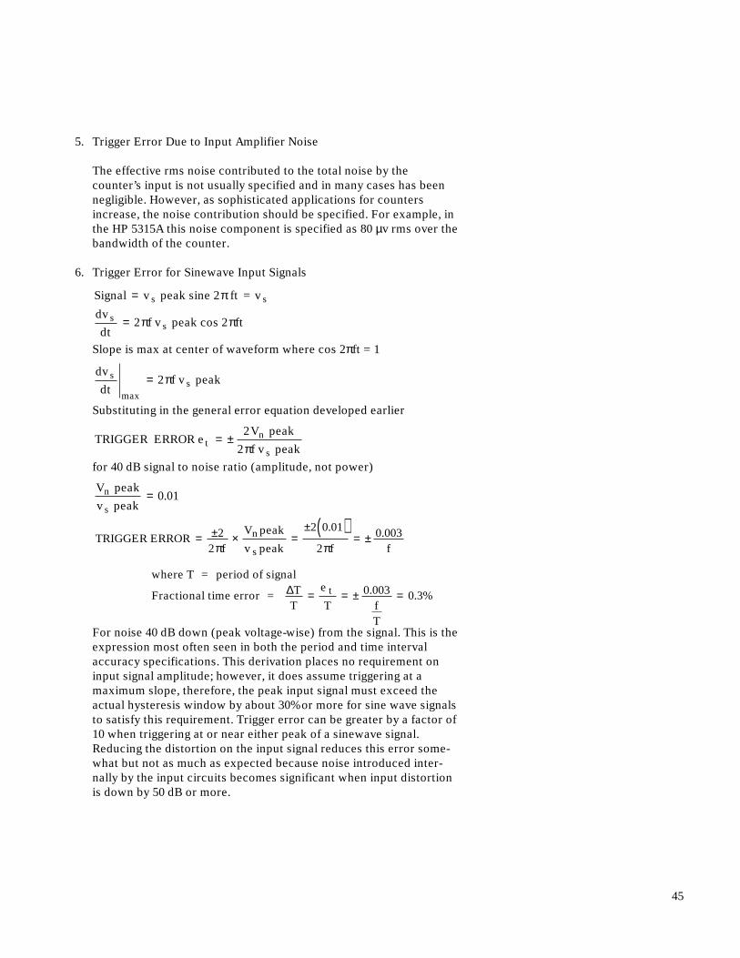
45
5. Trigger Error Due to Input Amplifier Noise
The effective rms noise contributed to the total noise by thecounter’s input is not usually specified and in many cases has beennegligible. However, as sophisticated applications for countersincrease, the noise contribution should be specified. For example, inthe HP 5315A this noise component is specified as 80 µv rms over thebandwidth of the counter.
6. Trigger Error for Sinewave Input Signals
Signal v peak
dv
dtf
s
s
=
=
sine 2 ft = v
v peak cos 2 ft
s
s
π
π π2
Slope is max at center of waveform where cos 2πft = 1
dv
dtfs
max
= 2π v peaks
Substituting in the general error equation developed earlier
TRIGGER ERROR e vt
s = ±
π2
2
V peak
f peakn
for 40 dB signal to noise ratio (amplitude, not power)
V peak
peakn
s v= 0 01.
TRIGGER ERROR
where T = period of signal
Fractional time error = TT
= ± × =± ( )
= ±
= = ± =
22
2 0 01
20 003
0 003 0 3
π πf
V peak
v peak f f
e
T fT
n
s
t
. .
. . %∆
For noise 40 dB down (peak voltage-wise) from the signal. This is theexpression most often seen in both the period and time intervalaccuracy specifications. This derivation places no requirement oninput signal amplitude; however, it does assume triggering at amaximum slope, therefore, the peak input signal must exceed theactual hysteresis window by about 30% or more for sine wave signalsto satisfy this requirement. Trigger error can be greater by a factor of10 when triggering at or near either peak of a sinewave signal.Reducing the distortion on the input signal reduces this error some-what but not as much as expected because noise introduced inter-nally by the input circuits becomes significant when input distortionis down by 50 dB or more.
46
7. Trigger Error Expression for Pulses
TRIGGER ERROR IN TIME, eV peak
Signal SlopeStart Channel
V peak
Signal SlopeStop Channel
tn n= ± +
For a counter with 100 mV rms sensitivity the hysteresis window =100 mV × 2.82 = 282 mV
For a 40 dB (amplitude) signal to noise ratio the peak-to-peak noisefor a 100 mV rms signal is 2.82 mV and peak noise is 1.41 mV.
Therefore:
Trigger error, et, for one channel = ( . .1 41 0 00141 mV)
Signal Slope Volt
Signal Slope=
TOTAL TIME INTERVAL ERRORSignal Slope ofstart channel
Signal Slope ofstop channel
≈ ± ±0 00141 0 00141. .
where signal slope is in volts per unit time
This derivation does depend on the input sensitivity of the counter(100 mV rms used for this example) so the expression will bedifferent for counters with other input sensitivities. Start channelslope and noise and stop channel slope and noise may not be thesame so must be evaluated individually for each channel.
8. Combining the Effect of Input Signal and Counter Contributed Noise
The rms noise associated with a single trigger is
X en2 2+
Input slew rate at trigger point
where X = effective rms noise of the counters input channel(= 80 µV for the HP 5314A and HP 5315A)
en = rms noise voltage of the input signal measured over a band-width equal to the counter’s bandwidth.
Since for time interval measurements trigger error occurs at boththe start and stop signals and the noise adds on an rms basis, therms trigger error for time interval measurements is
1 4 2 2. X en+Input slew rate at trigger point
s rms
47
In most cases, the dominant noise component is contributed by theinput signal. If the input signal is especially “quiet” the input amplifi-ers become a consideration. The fast slew rates of modern logicgreatly reduce the effect of noise errors and in many practical casesthese can be neglected.
9. Energy Effect
In addition to the previously discussed factors which contribute tothe trigger point time error, the so called “energy effect” is also afactor to consider when measuring intervals of a microsecond orless. This effect although always present is small enough so it isgenerally overshadowed by noise and other factors when measuringlonger intervals. The energy effect comes about because the inputvoltage must remain beyond the selected trigger voltage point longenough to transfer a finite amount of change, represented by theshaded area of Figure 31 into the trigger circuit to activate it. Theamount of change necessary to initiate triggering is a function ofboth the input amplifier-trigger sensitivity and the circuit bandwidthso may be different for each model of counter. Due to this effect, thecounter always triggers at a higher voltage (or lower depending onselected slope) than selected so in all cases the measurement beginsor ends later in time than expected.
The time error due to “energy effect” can be minimized by selectingtrigger points well within the maximum excursion of the signal. Forthe HP 5363B Time Interval Probes the specification requires thesignal to go beyond the selected trigger voltage point by at least100 millivolts or the trigger voltage selected must be below the peakby 8% or more of the peak-to-peak input voltage.
The energy effect error is negligible for long time intervals and whentriggering the start and stop channel at the same voltage point oninput signals with identical risetime and amplitude as when makingphase measurements. It does, however, require careful consideration
Figure 31.
Energy effect
introduces time
error ∆T which
can be significant
on short TI
measurement if
signal does not
extend well
beyond the
selected trigger
point.
Time
Inpu
t Vol
ts
0
Circuit Triggers
Selected Trigger Voltage Point
Input Signals
∆T1 ∆T2

48
when making risetime measurements on fast pulses as this calls forsetting one trigger voltage point near one extreme and the othernear the opposite extreme of the input signal.
This discussion points up the need for identical start and stopchannels when making sophisticated TI measurements on fastsignals. All circuits introduce some delay, but if start channel andstop channel delays are equal, the accuracy of the measurement isunaffected even though displaced in time. Identical amplifiers aremost apt to satisfy this requirement. Amplifiers with differentbandwidths will introduce error as the internal time constants arelonger, hence propagation delay is greater for low frequencyamplifiers.
± Time Base Error
Crystal oscillator (clock) accuracy is seldom of consequence in practi-cal time interval measurements. Most electronic counters have quartzoscillators with accuracy of a part in 106 (1 part per million) or better.As a result, the effect of oscillator stability does not affect a timeinterval measurement unless the display has 5 or 6 valid digits ofinformation. While it is possible to measure long intervals with highresolution, most practical measurements today are rise time of fastsignals, propagation time through high-speed logic or on narrow pulses.Resolving a 5 µsec interval to 1 nanosecond entails only 4 digits ofinformation — i.e., 5000 nanoseconds — so an oscillator as poor as1 part in a million introduces only 1/200 as much error as ±1 count forthis measurement. For shorter intervals the oscillator error is propor-tionally less.
Time interval averaging increases the number of valid digits, but hereagain usually not to the extent that crystal accuracy is important. Shortterm stability may become important when doing time interval averag-ing on narrow pulses. The short term stability specification is statisticalin nature so is worse for short averaging times. Consider for example ashort term accuracy specification of 1 × 10⁻⁹ for a 1 second averagingtime. This would be 1 × 10⁻³ for a 1 sec averaging time (5 nanosec forthe example above) and would be greater for an oscillator with poorershort term stability.
Aging rate is generally of consequence only in an application wherethe counter is used to make phase or time measurements to comparehigh precision frequency standards. In this application a counter is usedto measure the time variations between once per second time ticksfrom the two different frequency standards. Each time interval mea-surement may be as long as one second (1 × 10⁶ µsec) on frequenciesthat are stable 5 parts in 1012 or better so a stable crystal oscillator isneeded.
49
± Systematic Error
These fixed errors introduced by interconnecting cables, trigger levelsettings and similar parameters introduce errors which are essentiallyconstant for any given measurement configuration. Since these errorsare relatively constant they are of importance only when makingabsolute measurements of width, delay, etc., and do not enter in whenlooking for changes in the measured parameter as an experimentprogresses. Particularly on short intervals, the difference in delay due topropagation time on both the interconnecting cables as well as throughthe start and stop channel circuits may no longer be insignificant. Thisdifferential delay must either be adjusted out or taken into consider-ation when making absolute measurements. This error is usually smallso that it need not be considered when making measurements longerthan 10 microseconds or so. Signal propagation time is about 0.052nanosecond/centimeter (19.2 cm/ns) for polyethylene insulated RG 58A/U 50 ohm coax cable, therefore cable lengths must be matched for thestart and stop channels or the measurement may be in error. In mostmeasurement situations, the use of equal length cables cancels out thiserror; however, cable delay varies with the dielectric constant of theinsulation so cables of the same kind should be used. Where this is notpractical, the electrical lengths of the cables can be measured by thecounter to determine a correction factor to apply to the counter reading.Application Note 174-10, Measuring Electrical Length (Delay) of
Cables, discusses this measurement in detail.
Just as with other measuring instruments looking at fast rise inputsignals, one must also consider the fact that the loading introduced byconnecting the timer interval counter may actually change the shape ofthe input signal. The resistive component of loading is usually highenough so as not to be troublesome, rather it is the input capacity of thecounter and of the interconnecting cables that accounts for the loading.The HP 5363B Time Interval Probes box reduces this loading as far asfeasible for a general purpose instrument.

50
Time Intervals by Digital Interpolation
Digital Interpolation
Another technique for improving resolution is by interpolation which isa method of directly resolving the ±1 count inherent in digital countingschemes. A principle advantage of interpolation over averaging is thatthe technique does not depend on a repetitive signal for high resolution.In the HP 5370A the interpolation scheme provides 20 ps single shotresolution. If this is compared to a conventional scheme where cyclesof the internal time base are counted, it is the equivalent resolution thatwould be achieved by using a 50 GHz clock. Such clock frequencies are,of course, well beyond the present state of the art.
Another advantage of interpolation is that the high single shot resolu-tion allows the collection of meaningful statistical information. Impor-tant characteristics concerning time intervals like max., min., standarddeviation may be collected in addition to the mean. If fast data collec-tion facilities are available full histographical information may beobtained. In many time interval measurement situations, these statisti-cal properties are of prime importance. For example, in a digitalcommunication system where jitter is an important consideration, thestandard deviation gives an excellent indication of this.
Phase-Startable Phase-Lockable
Oscillators (PSPLO)
Precision digital interpolation schemes are based on phase-startable-phase lockable oscillators (See HP Journal, August 1978). Theseoscillators have two essential characteristics
1) When triggered oscillation will start, virtually instantaneously, andwith a fixed phase relationship to the external trigger pulse.
2) Once oscillating the stability of the frequency is preserved by phaselocking to a stable source such as a quartz oscillator.
The Dual Vernier Method
A precision dual vernier method of interpolation similar to that used inthe HP 5370A is shown in Figure 32. This system uses phase startablephase lockable oscillators in both the start and stop channels. Theseoscillators have a slightly longer period of oscillation than the referenceoscillator such that once started, they will reach coincidence with thereference oscillator some number of cycles later dependent on theinitial phase. If the reference oscillator period is T0 then the start andstop oscillators have periods equal to T0 + T0/N where N is the interpo-lation factor. From the diagram, it can be seen that the required timeinterval T may be evaluated as follows:
T = T1 – T2 + T3
= T0 (N0 + (1 + 1/N) (N1 – N2))

51
where N1 = Number of start oscillator pulses to coincidence
N2 = Number of Stop oscillator pulses to coincidence
N0 = Number of reference oscillator pulses between start andstop is incidence.
In the HP 5370A the reference oscillator has a period of 5 ns and thestart and stop oscillators have periods equal to
(5 ns + 5 ns/256) = 5 1 1256
+
ns .
This allows time to be resolved to 5/256 ns ≅ 20 ps.
A practical limitation on the interpolation factor N is imposed by theinherent noise in the counter’s input and other circuitry. If the typicalnoise jitter is say 35 ps rms, there is little advantage to be gained byhaving an interpolation factor capable of giving resolutions substan-tially better than this. Furthermore, the coincidence detection betweenthe interpolators and the reference clock would need to be done with acorrespondingly high time discrimination. This also imposes a practicallimitation. The dual oscillator scheme described above will operateregardless of whether the start or stop oscillator commenced first. Inthe HP 5370A if the stop signal arrives first, the time interval is given anegative sign.
Figure 32. Digital
Interpolation
Scheme using
phase-startable
phase-lockable
oscillators.
Digital Vernier Interpolation in the HP 5370A
Reference Oscillator
Start Coincidence
Stop CoincidenceStart
Stop
T
T1
T0 = 5 ns
T0 + T0/256= 5.02 ns
N1
N0
N2
T2
T3
5.02 ns
5 ns
0 1 2
0 1 2
0 1 2
3
TI = 5 [ 1.004 ( N1 – N2 ) + N0 ] ns

52
Phase-Startable Phase-Lockable Oscillators
Phase-startable phase-lockable oscillators (PSPLO) as described in theforegoing section may also be used for the generation of very precisedigital delays as in the HP 5359A Time Synthesizer. Here the output fromthe PSPLO is counted digitally in a preset counter to generate a veryprecise delay. An important benefit derived from using PSPLOs is thatthe phase with which the delay commences being synthesized has aconstant relationship to an external trigger signal. By contrast, a moreconventional scheme would involve interrupting an internal clock trainat some random phase resulting in a time interval being generated whichis subject to + or – one period variation of the clock.
A simplified block diagram of the HP 5359A and the timing relationshipbetween pulses is shown in Figure 33.
The Generation of Precise Time Intervals
Figure 33. Block
Diagram for the
HP 5359A Time
Synthesizer
showing timing
relationships
between output
pulses.
Ext Trigger
Digital Sync Delay
Microprocessor Controller
Power Supply
HP-IB Interface
Auto Calibrate
Digital Delay #1 0–160 ms
in 10 ns Steps
Startable Oscillator
(Lock to Xtal)
Events Count Ext Timing
Compensation
Analog Delay #2 0–10 ns
Analog Delay #1 0–10 ns
Digital Delay #2 0–160 ms
in 10 ns Steps
AutoSync Out
Output
Preset
S
R
Q
Ext PulseDelay (Fixed)
Delay 0–160 mS
35 ns Nominal
Width 5 ns–160mS
Sync Out
Output
35 ns NominalEdge 1
Edge 2
TD TW

53
Here the digital delay #1 determines the time from the sync output pulseto the output (TD) and digital delay #2, which causes the SR flip flop tobe reset, determines the width of the output pulse. Both digital delayswhich operate with 10 ns resolution are followed by analog delayswhich provide resolution from 0 to 10 ns. An interesting feature of thedelay scheme is the auto calibrate facility which calibrates the delaysincluding the analog portion back to a reference crystal oscillator. Sincethe instrument contains a microprocessor, any variations can beautomatically compensated for. This scheme allows generation of timeintervals with sub-nanosecond repeatability even at large delays of upto 150 ms.
The instrument is useful as a calibration source in Radar and othernavigation systems. For example, the sync output could be used tosimulate the send pulse, and the output which is precisely controllablein time could be used to simulate the return pulse corresponding to acertain range.
The instrument also has many general purpose laboratory applicationsin circuit design where it may be used as an extremely controllabledelay line for the investigation of circuit tolerances and race conditions.

54
Solve Troublesome TI Measurement Problems
The HP 5363B Time Interval Probes box, Figure 34, is a signal condi-tioner which solves the most troublesome problems encountered inmaking time interval measurements using an electronic counter:*
1 . By reducing circuit loading.
High impedance, low capacitance, active probes let the operatortransport the measurement point to the circuit under test. Thiskeeps circuit loading to a minimum as the usual interconnectingcables are no longer required for the input signal. This is particularlyimportant when working with pulses on other than 50 ohm systems.
2. By accurately defining the trigger voltage point.
A simple calibration procedure after SLOPE selection accuratelysets triggering at zero volts and calibrates out the residual offsetvoltages using digital techniques. Once calibration is completed, thetrigger point voltages are accurately determined by digitalthumbwheel switch settings.
3. By calibrating out differential delay between the start and stopchannels.
A second calibration step lets the operator calibrate out all of thedifferential delays in the system including those in the time intervalcounter start and stop channels as well as the interconnectingcables. An additional control position on the HP 5363B inserts afixed 10 ns delay in the stop channel so a counter such as the
Time Interval Measurement Using theHP 5363B Time Interval Probes
Figure 34.
HP 5363B Time
Interval Probes
* Active Probes improve precision of Time Interval measurements,
HP Journal, October 1975, Volume 27, Number 2, pp. 11-16.

55
HP 5345A which requires a minimum of 10 ns between a start pulseand the following stop pulse can be used for measurements down tozero nanoseconds. Figure 35 illustrates this procedure.
4. By offering greater dynamic range than counter inputs.
The start and stop channels of the HP 5363B are designed for allinput signals including those with large voltage vs time excursionsso will accept signals over the range of –10 volts to +10 volts withoutsacrificing sensitivity. This is particularly important when triggeringfrom many of the currently used IC logic levels. Logic swings are toolarge for the X1 range of most counters but sensitivity is sacrificedon the X10 or X20 range.
5. By offering remote programming for system applications.
Option 011 to the HP 5363B provides full remote programmingcapability including probe selection, SLOPE, POLARITY, LEVEL,and LEVEL CALIBRATION by a controller on the HP Interface Bus.The TIME ZERO control is not bus programmable; however, thedifferential delay can be measured and software adjusted in asystem.
0
0
0+0.5
–0.5
–0.5
+0.5Internally generated fast rise calibrate signal. Routed to both Start and Stop channels.
a. Block Diagram
b. Internally generated time calibration signal appearing of calibrate jacks on the front panel. Incorrect setting of the SLOPE switches of the counter will result in a counter display of approximately 7 µsec, the pulse width, or 49 µsec, the space between pulses.
Calibrate Connectors
"A" Probe
"B" Probe
Stop
10 ns
Stop
Start
Time Zero –0+In
put P
robe
s
VREF
VREF Pull to add
10.00 nsec
Subtract 10 ns from measurement
Output to time interval counter into 50Ω load
Stop
0+0.2
–0.2 ≈7 µsec≈49 µsec
≈
Volts
Figure 35.
Calibrating TIME
ZERO of the
HP 5363B to
compensate for the
differential delay
between the Start
and Stop Panels of
the Measuring
System.
56
Level Calibration
1. Depressing the LEVEL CALIBRATION switch first sets both theSTART LEVEL and STOP LEVEL voltages (normally determined bythumbwheel switches) to zero and grounds the tips of both PROBE Aand PROBE B which are inserted in the calibration connectors.Calibration can also be done by grounding the probe tips through50 ohms or less in systems applications, as it may not be convenientto use the calibration jacks.
2. The HP 5363B employs two DACs (digital to analog converters) fortrigger point setting and self calibration.
a. The main DAC, controlled by a thumbwheel switch, suppliestrigger level voltages settable from +9.99 to –9.99 V in 10 mVsteps.
b. The offset DAC, used to calibrate out residual offset voltages ofthe two probes, is initially offset from the main DAC by +75 mV,and covers the range from +75 mV to –75 mV in 1 millivolt steps.
c. When calibrating for a positive slope, the LEVEL calibrate switchloads zeros into the main DAC and zeros (represent +75 mV) intothe offset DAC.
Internal calibration circuits then scan the offset DAC voltageoutput which determines VC from +75 millivolts downward in1 millivolt steps until the input channel just switches triggeringat zero volts as in Figure 36. This voltage VC is stored digitally andadded to the digitally selected trigger voltage from thethumbwheel controlled DAC to give a true trigger point voltagewith respect to zero volts dc for subsequent measurements.
d. When calibrating for a negative slope, the process is similarexcept the offset DAC starts from –75 mV and scans upward.

57
3. The TRIGGER LEVEL OUTPUT voltage appearing at a rear BNCconnector (Figure 37) is the trigger voltage set on a thumbwheelswitch plus the calibration voltage supplied to the start or stopchannel by the offset DAC. Therefore, this level could be off asmuch as ±75 millivolts (the range of the offset DAC) from the actualtrigger voltage. This voltage can be displayed on an oscilloscopealong with the input signal to get an approximate idea of the triggerpoint location as an aid to initial set up. In practice the offset will bemuch less for an HP 5363B operating in a moderate environment.(Nominal offset voltage is –10 mV to –30 mV at room temperature.)The offset DAC voltage is present at the TRIGGER LEVEL OUTPUTon the rear panel after calibration when the associated thumbwheelLEVEL switch is set 0.00 and can be measured with a dc voltmeter.
4. LEVEL CALIBRATION must be done if the HP 5363B has beenturned off or at any time the SLOPE switch or PROBE selectorsettings are changed or trigger voltage errors as great as ±75 mV canoccur.
5. An easy way to determine spacing between the hysteresis limits isto go through the normal calibration procedure using a plus slope( ) and measuring the voltage output from the TRIGGER LEVELOUTPUT connector, then repeat the same procedure with thechannel set to trigger on a minus ( ) slope. The difference betweenthese two voltages is the spacing between the hysteresis limits towithin a few millivolts.
Figure 36. Level Calibration of one channel of one probe to trigger on a positive slope.
Input Grounded for Level Calibration
Offset DAC Voltage
a. Offset D to A converter scans VC down from +75 in 1 millivolt steps.
Probe
+75
–75
0
+75 mV
0
Operate
VC from Plus V Thumbwheel Switch
VC
VCMill
ivol
ts
Level Cal
Output
Hysteresis Window
Trigger at Zero volts on Positive Slope
b. Hysteresis window scans down until upper limit just crosses zero volts (ground) to trigger the circuit.
Trigger Level Output
Ref Voltage

58
Time Zero Calibration
Figure 35a (page 54) shows how the TIME ZERO calibration is madeusing an internally generated fast rise signal, Figure 35b. This calibrationcan also be done by using an external signal with fast transition time(>100 V/µsec slew rate) and setting both channels to the same triggerpoint (slope and level) preferably near the center of the input transition.
Figure 37. HP 5363B Controls and Connectors
Programmable(except delay
adjust) viaHP Interface Bus
Range+9.99 to –9.99Vin 10 mV steps
SelectSlope
Select Probe A,Probe B, or both
Status LightsIndicate probe selection
Self Calibration• Amplitude accuracy
• Delay error elimination
Low Capacitance Active ProbesTake HP or Tektronix® R.F. Oscilloscope
Probe Accessories
Main output tocounter, +0.5 to –0.5V
50Ω. Use counterin “PRESET”
Trigger level outputsfor Oscilloscope
Programming Capabilityvia HP Interface Bus

59
To Make a TI Measurement Using the HP 5363B
First determine that the signal is within the range of the HP 5363B.
1. Maximum input voltage to the HP 5363B probes without damage is±30 volts dc + peak ac! Minimum pulse width is 5 ns and maximumrepetition rate is 10 MHz. Other considerations are discussed inFigure 38. The trigger point is adjustable over a ±9.999 volts range in10 mV steps either by thumbwheel switches or via the HP interfacebus using Option 011.
CAUTION
KEEP PROTECTIVE GROUNDING CAPS ON PROBES WHENNOT IN USE OR WHEN SHIPPING TO PREVENT DAMAGE FROMSTATIC CHARGES.
2. Set Stop and Start PROBE selectors to A or B, SLOPE or ,polarity + or – and LEVEL of each channel as required for themeasurement of interest. Perform LEVEL calibration as discussedearlier in D.(d).
3. Connect the probe or probes to the input signal and make themeasurement.
NOTE
Perform LEVEL calibration any time the PROBE selector or SLOPEswitches are changed as the offset calibration for the new conditionis not made unless this is done. Calibration may not be necessarywhen measuring high amplitude input signals as maximum triggervoltage error without voltage calibration < ±100 millivolts.
4. Make your measurement with confidence!
Figure 38.
Input Signal
requirements for
the HP 5363B.
Stop
9.99 Vmax to –9.99 Vmin linear range
Start
Trigger Level 8% or 100 mV*
8% or 100 mV*Trigger Level
0
Trigger points should be below the peak pulse amplitude by 8% of peak-to-peak amplitude or 100 mv minimum to reduce energy effects.
Accurate triggering precludes triggering at the extremes of a waveform due to noise on slow rise pulses and “energy effect” on fast rise pulses. Signal must remain beyond the trigger point for a minimum of 5 ns. After triggering the signal must swing beyond the trigger point in the opposite direction for a minimum of 5 ns. At maxi- mum rate the HP 5363B will trig- ger on every cycle of a 100 MHz symmetrical square wave or sine wave of sufficient amplitude.
a.
b.5 nsec
min
5 nsec min
Within specified accuracy range, whichever is greater
*

60
Simple Timing System with Start-Stop
Pulses Generated by Mechanical Switches
The simplest time interval measuring system consists of a time intervalcounter, a voltage source, two mechanical switches, and two resistorsconnected as shown in Figure 39.
Even with this simple circuit of Figure 39 precautions must be taken toget valid measurements.
1. The SEPARATE-COMMON switch on the counter must be set toSEPARATE or both inputs will be tied together internally.
2. The voltage at the counter inputs goes from 0 to +1.5; therefore theLEVEL switches must be out of the PRESET position and set totrigger at about 0.7 volts. The system may work in the PRESETposition; however, triggering could be erratic as the operator isdepending on noise and overshoot caused by switch operation togenerate a signal that will cross the lower hysteresis limit.
Alternately, the inputs may be ac coupled; however in this case, it isvital that resistors R1 and R2 be used. If not, the counter will triggeronly once the first time a key is closed but will not trigger on subse-quent closings.
This happens because the coupling capacitor (either in the counteror in the external circuit) is initially discharged so it charges andtriggers the counter the first time the key is closed. With the keyopen this charge leaks off very slowly as the only discharge path isvia the leakage resistance of the capacitor so discharge may takefrom minutes to hours depending on the quality of the capacitor.Until this charge is dissipated, the circuit cannot be retriggered. The10k resistor R1 or R2 insures the coupling capacitor discharges in asmall fraction of a second once the key is opened, consequently theinput circuit will trigger each time the key is operated.
Some Applications of Time Interval Measurement
Figure 39. Simple
Time Interval
measuring System
– +1.5 Volts
Start Start
Stop
Coax Cable
TI Counter
Stop
K1
K2R1 10K
R2 10K

61
This system works very nicely using microswitches, telegraphkeys, or other mechanical switches to START and STOP the count.Start and Stop must be from separate switches and the counterSEPARATE/COMMON switch must be in SEPARATE for correctoperation.
3. This system will generally not make a pulse width measurementwith the counter set in COMMON (both Start and Stop input con-nected together internally) and the time interval controls set to Starton a voltage rise (positive slope when the switch is closed) and stopon a voltage fall (negative slope when the switch is opened). It doesnot work because mechanical switches exhibit contact bounce sothe counter displays the time of the first bounce rather than thetimes the switch was closed. This is discussed under Delay
Control and illustrated by Figure 22a.
For counters without a built-in delay circuit in the start channel, onecan be assembled from a single SN74121 or similar integratedcircuit, a 5-volt dc supply, one resistor, and one capacitor. The “on”time of this delay circuit, is made greater than the contact bouncetime of the start channel by selecting appropriate values of R and C.A 1-µfd capacitor and 10k to 20k resistor gives an “on” time of 10 to20 milliseconds which is adequate for most mechanical switches orrelays. A delay is not needed in the STOP channel as “off” time iscontrolled by the SAMPLE RATE control on the counter.
This same delay circuit is also needed to count the number ofoperations of a mechanical switch using a counter in a TOTALIZEmode. Without it, the counter counts and displays each contactbounce as well as each desired operation.
Phase Measurement
Phase measurement as made with an electronic counter is an importantspecial case of a time interval measurement. First the period a-b ismeasured, then the Time Interval a-c. From this information phase iscalculated using the formula:
Phase in degrees =t
T0 × 360

62
The general setup as in Figure 40 is the same as for any other timeinterval measurement; however, several factors must be considered toinsure the greatest possible accuracy in phase measurement.
1 . For any stable phase measurement, the frequency of the referencephase and the unknown phase must be identical.
2. Although a phase measurement could be made between any corre-sponding points on the two signals this method works only if bothsignals have the same constant amplitude otherwise the measure-ment will not yield absolute phase.
3. Set both the START and STOP channels to trigger at zero volts usingthe procedure of Figure 14 to get absolute phase. Triggering at zerovolts also has the added advantage that the phase measurement isindependent of input signal amplitude. When triggering at any pointother than zero, amplitude variations to either input channel show upas changes in the phase as measured by the counter. The HP 5363ATime Interval Probes are ideal for phase measurement as an internalcalibrate procedure plus setting both the START and STOPthumbwheel switches to zero assures triggering at precisely zerovolts dc.
4. Measure the time (T), Figure 40, by making a period average mea-surement. A period averaging measurement reduces the trigger errorbelow what it would be if the time interval mode were used sinceperiod measurements use the same trigger circuit and consequentlythe identical trigger voltage point for both Start and Stop.
5. Use the highest input amplitude available provided it does notexceed the internal protective clamp voltages of the counter. Ahigher amplitude signal increases the slope of the signal at the triggerpoint (zero volts) and thus reduces trigger error. If clamp voltagesare exceeded, however, the counter input impedance changesdrastically above the overload point and this distorts the input signalwhich in turn invalidates the desired time vs. voltage informationneeded for the measurement.
Figure 40. Phase
measurement with
a time interval
counter.
a
t0
c
Counter stops countingCounter starts counting
Reference PhaseUnknown Phase
where:Period of reference phase in µsec Time difference in µsec between the positive going zero axis crossings of the reference phase (START) channel and the unknown phase (STOP) channel.
T t0
= =
b
Period of RefT
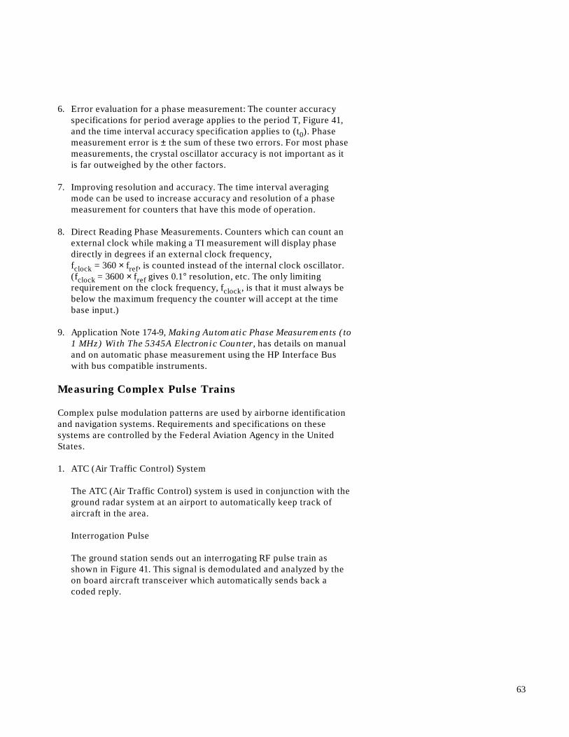
63
6. Error evaluation for a phase measurement: The counter accuracyspecifications for period average applies to the period T, Figure 41,and the time interval accuracy specification applies to (t0). Phasemeasurement error is ± the sum of these two errors. For most phasemeasurements, the crystal oscillator accuracy is not important as itis far outweighed by the other factors.
7. Improving resolution and accuracy. The time interval averagingmode can be used to increase accuracy and resolution of a phasemeasurement for counters that have this mode of operation.
8. Direct Reading Phase Measurements. Counters which can count anexternal clock while making a TI measurement will display phasedirectly in degrees if an external clock frequency,fclock = 360 × fref, is counted instead of the internal clock oscillator.(fclock = 3600 × fref gives 0.1° resolution, etc. The only limitingrequirement on the clock frequency, fclock, is that it must always bebelow the maximum frequency the counter will accept at the timebase input.)
9. Application Note 174-9, Making Automatic Phase Measurements (to
1 MHz) With The 5345A Electronic Counter, has details on manualand on automatic phase measurement using the HP Interface Buswith bus compatible instruments.
Measuring Complex Pulse Trains
Complex pulse modulation patterns are used by airborne identificationand navigation systems. Requirements and specifications on thesesystems are controlled by the Federal Aviation Agency in the UnitedStates.
1. ATC (Air Traffic Control) System
The ATC (Air Traffic Control) system is used in conjunction with theground radar system at an airport to automatically keep track ofaircraft in the area.
Interrogation Pulse
The ground station sends out an interrogating RF pulse train asshown in Figure 41. This signal is demodulated and analyzed by theon board aircraft transceiver which automatically sends back acoded reply.
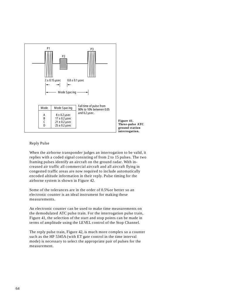
64
Reply Pulse
When the airborne transponder judges an interrogation to be valid, itreplies with a coded signal consisting of from 2 to 15 pulses. The twoframing pulses identify an aircraft on the ground radar. With in-creased air traffic all commercial aircraft and all aircraft flying incongested traffic areas are now required to include automaticallyencoded altitude information in their reply. Pulse timing for theairborne system is shown in Figure 42.
Some of the tolerances are in the order of 0.5% or better so anelectronic counter is an ideal instrument for making thesemeasurements.
An electronic counter can be used to make time measurements onthe demodulated ATC pulse train. For the interrogation pulse train,Figure 41, the selection of the start and stop points can be made interms of amplitude using the LEVEL control of the Stop Channel.
The reply pulse train, Figure 42, is much more complex so a countersuch as the HP 5345A (with ET gate control in the time intervalmode) is necessary to select the appropriate pair of pulses for themeasurement.
Figure 41.
Three-pulse ATC
ground station
interrogation.
P1
Mode Spacing
2 ± 0.15 µsec 0.8 ± 0.1 µsec
Mode
A B C D
Mode Spacing
8 ± 0.2 µsec 17 ± 0.2 µsec 21 ± 0.2 µsec 25 ± 0.2 µsec
P2
P3
Fall time of pulse from 90% to 10% between 0.05 and 0.2 µsec.

65
The EXT gate of the counter can be opened at any time following thelast pulse of the previous pulse train. The measurement will thenbegin with the next pulse to occur — in this case, the first framingpulse of the pulse train of interest at (a) in Figure 43.
A pulse generator with a variable pulse width (HP 8007A or similar)triggered by the GATE OUT of the HP 5345A is used to select thestop pulse. The counter stops the measurement on the input pulsefollowing the end of the pulse from the pulse generator (–1V to 0Vtransition). Pulse width setting is not critical as spacing betweenpulses of the input signal is about one microsecond. A circuit as inFigure 44 can be used to synchronize the measuring system withrespect to the first pulse in the complex pulse train shown.
Figure 42.
Available ATC
reply Pulse codes.
Demodulation Pulsed Signal
First Framing Pulse
Pulse of Interest
Exit Gate to Counter
TI MeasuredTime
–10
a b
First Framing
0.5 µsec1.45 µsec2.9 µsec 20.3 µsec
24.65 µsec
Last Framing
First Framing
500 µsec Min
Ident Pulse
Width Rise Time Fall Time Spacing
0.45 ± 0.10 µsec 0.05 to 0.10 µsec 0.05 to 0.2 µsec 1.45 µsec between each pulse accuracy ±0.10 µsec with respect to the first framing pulse. One pulse to any other pulse in the group except first framing pulse is ±0.15 µsec
Figure 43.
Making time
measurements
on an ATC
Transponder
replay pulse
with the HP5345A
Counter.
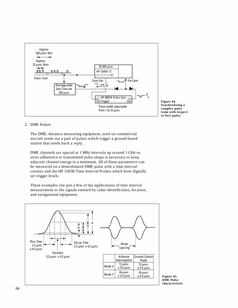
66
2. DME Pulses
The DME, distance measuring equipment, used on commercialaircraft sends out a pair of pulses which trigger a ground basedstation that sends back a reply.
DME channels are spaced at 1 MHz intervals up around 1 GHz sostrict adherence to transmitted pulse shape is necessary to keepadjacent channel energy to a minimum. All of these parameters canbe measured on a demodulated DME pulse with a time intervalcounter and the HP 5363B Time Interval Probes which have digitallyset trigger levels.
These examples cite just a few of the applications of time intervalmeasurement to the signals emitted by radar identification, location,and navigational equipment.
Figure 44.
Synchronizing a
complex pulse
train with respect
to first pulse.
Retriggerable One Shot mV
200 µsec
Approx 500 µsec Min
Approx 25 µsec Max
Pulse Train
Ext Trigger OutHP 8007A Pulse Gen.
Pulse width adjustable from 1 to 25 µsec
20,300 µsec
HP 5345A TI
Gate Out Ext Gate
0+1
–10
Figure 45.
DME Pulse
characteristic
Rise Time 2.5 µsec
± 0.5 µsec
Decay Time 2.5 µsec ± 0.5 µsec
Mode Spacing
Duration 3.5 µsec ± 0.5 µsec
0.1A
0.5A
A
Airborne Interrogation
Ground Station Reply
12 µsec. ± 0.5 µsec
12 µsec. ± 0.5 µsecMode X
30 µsec. ± 0.5 µsec
36 µsec. ± 0.5 µsecMode Y
0.9A
67
The oscilloscope was one of the first instruments used for pulse and risetime measurements, and it has been used in that role ever since. Bothoscilloscopes and time interval counters have specific advantages inmaking time interval measurements, and in many cases, the techniquesare complementary. In general, time interval counters give greaterresolution (0.00000001% on the HP 5370A) on pulse to pulse measure-ments and can be more readily automated. The oscilloscope givesexcellent visual feedback and recently, the introduction of ∆timeoscilloscopes has made a very real contribution to improving oscillo-scope resolution for time interval measurements. For example, theHP 1743A is capable of giving a resolution of 0.002%. ±1 count. Thevisual feedback characteristic of the oscilloscopes is important whendealing with noisy or complex waveforms as it allows a skilled operatorto concentrate only on the points of interest. If rise times are fast, a timeinterval counter will not be affected by noise, but in measurements withslow rise time, caution should be exercised.
Interpolating counters give very high single shot resolution which wouldnot be possible on a ∆time scope which requires a repetitive signal foroperation. In addition, this high single shot resolution of the interpolat-ing allows the collection of statistics.
From the user’s viewpoint, the characteristics of the measurement andoutput required will determine the most acceptable measurementsolution. The following summary may help in the selection process.
Time Interval Counter:
• Highest resolution in pulse to pulse measurements.
• Easy Automation — IEEE 488 Interfacing.
• Statistics.
• Noise effects negligible on fast rise time pulses.
• Single shot capability.
• Different trigger voltages on stop and start channels.
• Measurements above 100 MHz.
Oscilloscope:
• Excellent visual feedback
• Noisy complex waveforms may be visually filtered.
• Excellent for slow rise time measurements on noisy signals.
• Less prone to false triggering due to noise.
Comparison with Other Ways of Making Time IntervalMeasurements on Narrow Pulses or Fast Rise Signals

68
For more information about Hewlett-Packard test and measurement products,applications, services and for a currentsales office listing, visit our web site,http://www.hp.com/go/tmdir.You can also contact one of the followingcenters and ask for a test and measure-ment sales representative.
United States:
Hewlett-Packard CompanyTest and Measurement Call CenterP.O. Box 4026Englewood, CO 80155-40261 800 452 4844
Canada:
Hewlett-Packard Canada Ltd.5150 Spectrum WayMississauga, OntarioL4W 5G1(905) 206-4725
Europe:
Hewlett-PackardEuropean Marketing CentreP.O. Box 9991180 AZ AmstelveenThe Netherlands(21 20) 547 9900
Japan:
Hewlett-Packard Japan Ltd.Measurement Assistance Center9-1, Takakura-Cho, Hachioji-Shi,Tokyo 192, JapanTel: (81-426) 56-7832Fax: (81-426) 56-7840
Latin America:
Hewlett-PackardLatin American Region Headquarters5200 Blue Lagoon Drive9th FloorMiami, Florida 33126U.S.A.(305) 267 4245/4220
Australia/New Zealand:
Hewlett-Packard Australia Ltd.31-41 Joseph StreetBlackburn, Victoria 3130Australia1 800 629 485
Asia Pacific:
Hewlett-Packard Asia Pacific Ltd.17-21/F Shell Tower, Time Square,1 Matheson Street, Causeway Bay,Hong KongTel: (852) 2599 7777Fax: (852) 2506 9285
H
Data Subject to ChangePrinted in U.S.A. June 1997
Hewlett-Packard CompanyCopyright © 19975965-7663E