Fundamentals and applications of integrated circuits.
220
FUNDAMENTALS AND APPLICATIONS OF INTEGRATED CIRCUITS Daniel Leonard Wojtkowiak
Transcript of Fundamentals and applications of integrated circuits.

FUNDAMENTALS AND APPLICATIONSOF INTEGRATED CIRCUITS
Daniel Leonard Wojtkowiak

DUDLEY KNOX LIBRARYNAVAL POSTGRADUATE SCHOOLMONTEREY. CALIFORNIA 93840
MV1
Monter o ! if
y
iau *its£i-y
J;;
UlllllT'll B—
—
FUNDAMENTALS AND APPLICATIONSOP
INTEGRATED CIRCUITS
by
Daniel L. Wojtkowiak
Thesis Advisor: R. Panholzer
Approved for public release; distribution unlimited.
T170806


SECURITY CLASSIFICATION OF THIS PAGE (When Data Entered)
DUDLEY KNOX LIBRARYNAVAL POSTGRADUATE SCHOOLMONTEREY, CALIFORNIA 93940
REPORT DOCUMENTATION PAGE READ INSTRUCTIONSBEFORE COMPLETING FORM
1. REPORT NUMBER 2. GOVT ACCESSION NO 3. RECIPIENT'S CATALOG NUMBER
4. TITLE (find Subtitle)
Fundamentals and Applications ofIntegrated Circuits
5. TYPE OF REPORT ft PERIOD COVERED
Master's Thesis Dec 75
6. PERFORMING ORG. REPORT NUMBER
7. authorc*; 8. CONTRACT OR GRANT NOMBERf*.)
Daniel L. Wojtkowiak
9. PERFORMING ORGANIZATION NAME AND ADDRESS
Naval Postgraduate SchoolMonterey, CA. 939^0
10. PROGRAM ELEMENT, PROJECT TASKAREA ft WORK UNIT NUMBERS
II. CONTROLLING OFFICE NAME AND ADDRESS
Naval Postgraduate SchoolMonterey, CA. 939^0
12. REPORT DATE
December 197513. NUMBER OF PAGES
10614. MONITORING AGENCY NAME ft ADDRESSf// dllterent from Controlling Olllce)
Naval Postgraduate SchoolMonterey, CA. 939^0
15. SECURITY CLASS, (ol thla report)
UnclassifiedISa. DECL ASSIFICATION/DOWNGRAOING
SCHEDULE
16. DISTRIBUTION STATEMENT (of thla Report)
Approved for public release; distribution unlimited
17. DISTRIBUTION STATEMENT (ol the abatrtct entered In Block 20, II different Horn Report)
16. SUPPLEMENTARY NOTES
19. KEY WORDS (Continue on reverae aide It naceeamry end Identity by block number)
Fundamentals applications integrated circuits
20. ABSTRACT (Continue on reverae aide It naceeamry and Identity by block number)
A training program in the fundamentals and applications of inte-grated circuits has been developed. The program is designed forindependent study and contains coordinated laboratory exercisesused to reinforce each subject. The exercises are performed onan Analog/Digital Trainer, which consists of a group of modulesand an integrated circuit Breadboard. Circuits described in theindividual lessons are quickly realized on the Trainer to providethe student -with valuable "hands-o n" experience. Two sections J
BBnWJBBaaM*ajk»aaBBa*tSaaaU.*aaBMBBBBBaaaBBaaaB«.-«BBaBaaBBBaM
DD ,^M73 1473
(Page 1)
EDITION OF 1 NOV 6» !S OBSOLETES/N 0102-011- 6601 !
SECURITY CLASSIFICATION OF THIS PAGZ (»hen Del* Hnte'md)

JtCOKlTY CLASSIFICATION OF THIS PAGECW^en Orl< EnlaroJ
have also been Included which describe additions to the basicTrainer design.
DD Form 14731 Jan 73
_ .
S/N 0102-014-6601 SECURITY CLASSIFICATION OF THIS PAGECWhon D«t« Zntertd)


Fundamentals and Applications of Integrated circuits
by
Daniel Leonard tfojtkowiak
Lieutenant Commander, United States Navy
B.S.E.E., Naval Postgraduate School, 1974
Submitted in partial fulfillment of the
requirements for the degree of
MASTER OF SCIENCE IN ELECTRICAL ENGINEERING
from the
NAVAL POSTGRADUATE SCHOOL
December 1975

mes6

WAVAL POSTGRADUATE SCHOfti
ABSTRACT
A training program in the fundamentals and applications
of integrated circuits has been developed. The program is
designed for independent study and contains coordinated
laboratory exercises used to reinforce each subject. The
exercises are performed Da an Analog/Digital Trainer, which
consists of a group of modules and an integrated circuit
Breadboard. Circuits described in the individual lessons
are quickly realized on trie Trainer to provide the student
with valuable "hands-on" experience. Two sections have also
been included which describe additions to the basic Trainer
design.


TABLE OF CONTENTS
I. INTRODUCTION 11
A. INSTRUCTIONS FOR PERFORMING
LABORATORY EXERCISES 13
1. Lesson Objectives 13
2. Discussion * 13
a. Power Supply Selection 13
b. Breadboard Hints 14
B. TTL DESIGN CONSIDERATIONS 17
1. Lesson Objectives 17
2. Discussion 17
a. Power Supply Considerations 17
b. Input and Output Voltage Levels 18
c. Unused Inputs 19
C. OPEN-COLLECTOR AND TRI-STATE LOGIC • 20
1. Lesson Objectives 20
2. Discussion 20
3. Laboratory Exercises 24
a. Equipment 24
b. EXCLUSIVS-OR Circuit 24
c. Binary Half Adder -— 25
d. Binary Full Adder 26
e. Tri-State Logic Buss Selector-- 27


D. FLIP-FL3PS 28
1. Lesson Objectives 28
2. Discussion 28
a. RS Fiip-Flop 28
b. Master-Slave Flip-Flop-' 30
c. "T" Flip-Flop 31
d. JK Flip-Flop 32
e. Clocked-Logic 33
f. "D" Flip-Flop 35
3. Laboratory Exercises 36
E. ASYNCHRONOUS COUNTERS 38
1. Lesson Objectives 38
2. Discussion 38
a. Straight Binary and Feedback
Ripple Counters 39
b. Directional Counters- HI
c. TTL MSI Counters 42
3. Laboratory Exercises • 43
a. Equipment 44
b. Four-Bit Binary Counter 44
c. BCD Asynchronous Counter 44
d. TTL rtSE Counters 45
F. SYNCHRONOUS COUNTERS 46
1. Lesson Objectives 46


2- Discussion 46
a. Modulo-4 Synchronous Counters 47
b. BCD Synchronous Counters r 48
c. Combination Synchronous
Asynchronous Counters 49
a. TTL MSI Counters 50
3. Laboratory Exercises 51
a. Equipment 51
b. Modulo-4 Synchronous Counter 52
c. BCD Synchronous Counter 52
d. Combination Synchronous
Asynchronous Counter 52
e. TTL MSI Counters r 52
SHIFT REGISTERS 54
1. Lesson Objectives 54
2. Discussion 54
a. Basic Shift Register Classifications 54
b. Shift Counters 58
c. Pseudo-Random Binary Sequence
Genera toe 5 9
3. Laboratory Exercises 61
a. Equipment 61
b. Shift Counters and Pseudo-Random
Sequencers • 6 1

DECODERS 6 3
1. Lesson Objectives 63
2. Discussion 63
a. Display Decoders 63
b. Logic Decoders 66
3. Laboratory Exercises 67
a. Equipment 68
b. Logic Decoders— 68
OP-AMP CIRCUIT DESIGN 69
1. Lesson Objectives ' 69
2. DiscussioQ 69
a. Open Loop Voltage Sain 69
b. Slew Rite 71
c. Input Impedance 72
d. Output Impedance 76
e. Input Dffset Voltage 76
f. Input Offset Current 77
g. Common Mode Rejection 78
h. Stability 78
3. Design Procedures 82
a. Inverting Amplifiers 82
b. Non-inverting Amplifiers 86
4. Design Summary- k 91
a. Inverting amplifiers 91

b. Non-Inverting Amplifiers 92
II. ADDITIONS TO THE AN&LOG/DIGITAL IC TRAINER 94
A. MAIN FRAME POWER SUPPLY 95
1. Introduction 95
2. Operation 95
3. Specifications 96
4. Circuit Description 96
B. BINARY DISPLAY/LOGIC PROBE MODULE 100
1. Introduction 100
2. Operation 100
3. Specifications j— 101
4. Circuit Description— < 102
BIBLIOGRAPHY 105
INITIAL DISTRIBUTION LIST 106


ACKNOWLEDGEMENT
The author gratefully acknowledges the direction and
guidance of his advisor, Professor R. Panholzer, luring this
and other related projects.
10


I. INTRODUCTION
The nine sections that follow were designed as separate
instructional packages to reinforce the students knowledge
of the fundamentals and applications of analog and digital
integrated circuits (IC's). Each lesson can be accomplished
in approximately 1-3 hours. The lessons begin with stated
objectives, followed by a discussion of the circuit and its
applications. The transistor- transistor logic (TTL) family
of digital circuits is used exclusively due to its industry
wide acceptance. Laboratory exercises are included in each
lesson and are accomplished on an Analog/Digital IC Trainer
pictured on the following page. The Trainer consists of a
Main Frame, plug-in modules and an IC Brreadboard. The
modules called for in the lessons are plugged into the
Trainer and IC's are interconnected through the use of the
breadboard. Reference 1 contains a detailed description of
the Trainer.
11


ANALOG/DIGITAL INTEGRATED CIRCUIT TRAINER
12


A. INSTRUCTIONS FOR PERFORMING LABORATORY EXERCISES
1 . Lesson Objectives
The primary objective of this lesson is to make the
laboratory exercises that follow easy to perform. The
exercises were all designed to enable the student to retain
the key points of each lesson by reinforcing thesa points ia
a "hands-on" laboratory exercise. As is often the case,
hardware problems involved in performing a lab exercise
usually obscure the original goal. It is sincerely hoped
that this le-sson will eliminate these "cockpit" problems and
clear the way for an efficient learning experience.
2 • Discussion
Someone once said, "If all else fails; read the
instructions". This is especially true in this case.
Before using the Analog/Digital Trainer take tha time to
read the Trainer Instruction Manual [Ref. 1 ]. In it, each
module is described in detail along with its proper
operating procedure. Most important, a go-no-go test is
given for each module which will enable you to quickly
determine if the module is operating properly. This will
save you many hours of trouble-shooting a problem circuit,
when all along the equipment was faulty.
a. Power Supply Selection
After reading the instruction manual and
becoming familiar with the available modules, you are ready
to gather up the necessary equipment to perform your first
lab exercise. All the items that you will need for the
exercise are listed in tha Equipment section of aach lesson.
Note that there are two different Main Frames available.
One is marked "5 AMPS". This indicates the max current that
13


the 5 volt power supply is capable of providing. The
unmarked Main Frames are rated at 1.75 amps. Most of the
lab exercises can be performed safely on the lower rated
power supply. If you plan on using more modules than called
for in the lab exercise, or if you expand the number of
devices connected on the breadboard, ensure that you do not
exceed the power supply rating. If in doubt, add up the
current drawn by each module and the total current needed
tor the devices connected on the breadboard. Each module
requirement is listed in the instruction manual. While both
power supplies are protected from overload and short
circuit, it is not necessary or desirable for you to test
these features.
b. Ereadboard Hints
The Breadboard is the next item that can cause
you problems if yoj are not aware of how it is
interconnected. Remove the Breadboard from the Main Frame
and observe the back, side. Notice that the pins marked "V"
are interconnected in rows along the bottom side of the
board. This enables you to use IC's of different voltage
rating, as long as they are segregated by rows, and if the
rows are connected to the proper voltage through jumper
wires. If all the devices used will be of one voltage
rating, jumper the rows together at the right side of the
board. Do this at the start, as it is easy to forget to
power the devices. This simple step will save much
trouble-shooting time later. A word of caution. If 5 volt
and 15 volt devices are used together, it is advisable to
mark the higher voltage row with a piece of paper stuck on
the pins in that row. This should preclude installing 5
volt devices in that row. A TTL package will operate for
about 1 nano second on 15 volts, before it ceases to
function.
The wiring hints that follow might seem too
V*


basic and not worth mentioning. However, experience has
shown that it is time consuming to detect a wiring error in
a modest circuit with four to six ic's and almost impossiole
in larger circuits. The procedure recommended will add only
a few minutes to the wiring of a circuit, but could save
hours of trouble-shooting. With large circuits, it is
usually much faster and easier to find a wiring error by
removing all the wires and starting from the begining.
The individual socket pins are numbered with two
rows of numerals. The inside row goes from 1 to 7 on one
side, and 8 to 14 on the upper side. This inside row is for
use with 14 pin devices, while the outer row of numbers is
for use with 16 pin devices. The dual in-line package (DIP)
has an indentation or other marking over pin 1 on the
device. The pins are numbered counter-clockwise from pin 1
looking at the top of the device. As you can imagine, it is
important to insert the DIP in the socket properly so the
pin numbers match those on the board. The most frequent
cause of wiring error comes about by using the wrong row of
numbers. Before each connection is made to a DIP, observe
the package size. If it is small (14 pin), use the inner
rows; if large (15 pin), use the outer rows.
For large circuits (8 or more IC's), it is best
to start with a connection diagram of the circuit showing
pin numbers for each IC. The IC's are installed in the
breadboard in such a way as to minimize the distance between
packages that must be interconnected, while maintaining the
proper voltage row.
All wiring and IC installation is to be done
with the power switch on the Main Frame turned off. Tne
first step in wiring should be to connect the ground and "V"
lead to each IC. Using a colored pencil, trace over each
line on the connection diagram as the leads are installed.
It is best to run a lead direct from each IC to ground or
"V" rather than using the ground or "V" lead of an adjacent
package. While tnis type of interconnection is electrically
15

sound it makes trouble-shooting almost impossible.
After the power leads are connected to each IC,
it is advisable to turn the power switch on to ensure that
no shorts are present. It is easy to correct the problem
now before the other vires are installed. If ail is well,
turn off the power and continue with connecting the rest of
the circuit.
Select the next circuit that is common to all
the IC's, like the clock circuit. Interconnect this circuit
tracing over each wire on the connection diagram as it is
installed. In a similar manner complete the circuit a
common branch at a tirae. The final step should be the
interconnection of the modules for clocking or display etc.
This step by step method will almost guarantee
success and allow you to proceed with the exercise in the
minimum amount of time.
16

B. TTL DESIGN CONSIDERATIONS
1 • lesson. Qki§2tives
The electrical characteristics of TTL integrated
circuits must be thouroughly understood by the desiginer to
enable him to design efficient and dependable circuits.
This lesson is a gathering of the more important electrical
characteristics and design considerations that are essential
in attaining this goal.
2« Discussion
a. Power supply considerations
The TTL family of integrated circuits needs a single
5-volt positive supply that is well regulated. The maximum
variation allowed is ±250 mV. Because the totem-pole output
is used in most TTL IC packages, a large current spike is
produced which could effect the operation of other IC's
connected to the same power supply. To prevent these
current spikes from traveling through the supply lines,
despiking capacitors are used. These capacitors are disc
type, with a value of 0.1 to 0.01 mfd. As a general rule, a
despiking capacitor is used for every 2 medium scale
integrated (MSI) packages [ Ref . 2]. They are mounted close
to the IC's, using the shortest possible lead lengths. The
power distribution system must have low inductance to
prevent the interaction of TTL components with each other.
On a printed circuit board this can be achieved by using
wide runs for the supply and ground lines. The runs should
be one quarter inch or more in width. A good practice is to
use a ground plane system where the maximum unused portions
of the board are made part of the ground system. This
reduces the length of despiking capacitor leads and also
prevents ground loops from being formed.
17


b. Input and Output Voltage Levels
The input and output voltage levels needed for
proper operation of TIL gates must be clearly understood.
For logic level "0"/ the maximum voltage permitted at the
input of a standard or high speed TTL gate is 0.8 volts.
Voltages above this will cause the gace to oscillate or stay
in its active region. The maximum logic level "0" output
voltage is 0.4 volts. This allows the output to be directly
connected to the input of another TTL gate. The output
low-state also has the capability of sinking 16 mA. This is
refered to as a fan-out of 10, since when one input gate is
grounded, about 1.6 mA of current flows through the
grounding lead. The output-high state or logic level "1"
has a minimum voltage of 2.4 volts. The minimum input-high
is 2 volts. If two gates are cascaded, the output high will
provide 2.4 volts into the input or, 0.4 volts more than is
needed by the input. This same 0.4 volt margin is provided
for cascaded gates in the low state. Figure B-1 graphically
displays these voltage levels.
•v-5.0
2.0
+5.0
z.h
TRANSITION TRANSITION
0.0INPUT
0.4
0.0////"0"7 ,/ ,./
OUTPUT
FIG. B-1. TTL INPUT AND OUTPUT VOLTAGE LEVELS
18


c. Onused Inputs
An unused and unconnected TTL input will pull
itself to a high or logic level "1" state, and be highly
susceptible to noise. It is good engineering practice to
tie all unused inputs to +5 volts or to a logically similar
input. The proper ctoice depends on the type of gate
involved. All unused NAND, OR, AND inputs should be tied to
a used input of the same gate. This should only be done if
the high level fan-out of the driving circuit is not
exceeded. All unused NOR or OR inputs are tied to ground or
a used input of the same gate. Again, this later connection
should be made only if the fan-out of the driving circuit is
not exceeded. To provide a permanent logic level "1",
connect the input to +5 iirectly, or to +5 through a 1k ohm
resistor. The resistor will act as a current limiter to
prevent damage to the input circuit in the event of a
positive voltage excursion. A permanent logic level "0" on
an input is easily provided by tieing the input to ground.
Reference 3 recommends that the outputs of unused gates be
forced High by tieing all NAND or NOR gate inputs to ground..
This lowers the power dissipation and supplies a logic High
at the gate output which can be used at unused inputs to
other gates.
19

C. OPEN-COLLECTOR AND TBI-STATE LOGIC
1 • Lesson Object ives
The totem pole output circuit of TTL will be
reviewed to point out the hazards involved in using this
family of digital logic circuits in a wired logic
configuration. Safe implementation of wired logic will be
explained using open-collector and Tri-State logic families
with examples given for each.
2 • Disc uss ion
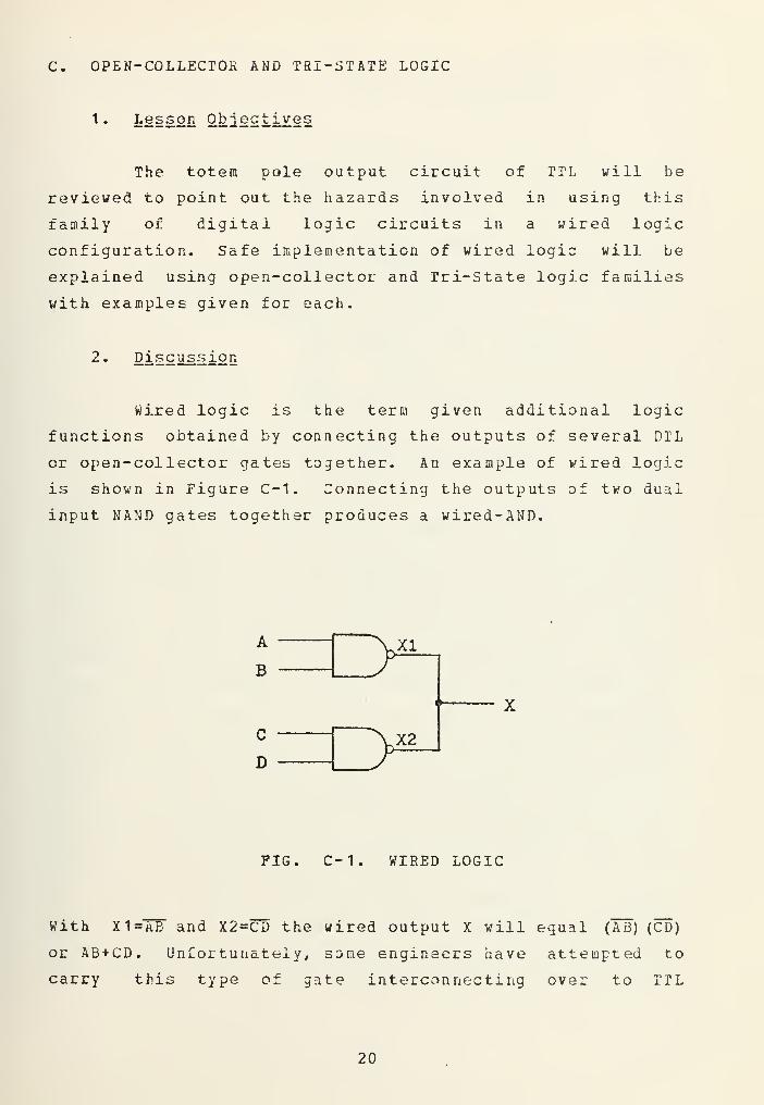
Wired logic is the term given additional logic
functions obtained by connecting the outputs of several DTL
or open-collector gates together. An example of wired logic
is shown in Figure C-1. Connecting the outputs of two dual
input NAND gates together produces a wired-AND.
A
B
C
D
XI
X2
FIG. C-1. WIRED LOGIC
With X1="kT and X2=CD the wired output X will equal (Tb) (CD)
or AB+CD. Unfortunately, some engineers have attempted to
carry this type of gate interconnecting over to TIL
20


circuits. The majority of l'TL packages utilize an
totem pole output circuit as shown in Figure C-2.
active
+5
IN
OUTPUT
FIG C-2. TOTEM POLE OUTPUT
In this circuit Q2 acts as a phase splitter Kith its
collector voltage out of phase with the emitter voltage.
When Q2 is driven into saturation QU is turned off and 03 is
turned on. This grounds or sinks the output resulting in a
low state. This grounding in the low state is why TTL is
sometimes refered to as current sinking logic. If Q2 is
turned off the voltage at its collector rises driving Q4
into saturation and turning off Q3. With no load connected,
the output will increase to Vcc minus the transistor voltage
drop or about 3.9 volts. During the transition from low to
high, or vice-versa, both transistors conduct heavily and
the current is limited only by the 100 ohm resistor and the
combined voltage drops of transistors Q4 and Q5. Since the
transition is very fast the current spike, which is usually
10 times the normal supply current, lasts for only 10
nanoseconds. If we connect the outputs of two different
gates together, as in wired logic, we have a problem when
the outputs try to assuue different states. The low output
21


will ground the five volt power supply through the high
output. Eecause of the 100 ohm resistor and various
transistor voltage drops, the current will be limited to
approximately HI raA. This is enough to destroy the output
transistor of the high logic gate. For this reason wired
logic must never be used with active totem pole output
circuits.
Most of the DTL family and some TTL components
utilize the open-collector output circuit. As an example,
an open-collector NAND gate (7U03) is shown in Figure C-3.
+5
INPUTS
2.2K PULL-UPRESISTOR
OUTPUT
FIG. C-3. NAND GATE OPEN COLLECTOR
With this type of output circuit wired logic may be used
provided a 2.2 K ohm pull-up resistor is added as shown.
With this circuit any number of open-collector outputs may
be connected together as the gates can only pull the outputs
down, not up. The output will swing positive only when none
of the gates are pulling down.
Problems arise when using several gates in the wired
logic configuration. First, the noise immunity of the basic
gate is decreased as tha number of gates tied together
increases. Second, system speed is reduced as resistor
22

pull-up can never be as fast as an active totem pole output.
Third, and the most important problem of all, there is no
easy way to trouble shoot a point that has several
open-collector gates tied to it. If one gate is defective
the entire circuit appears defective and isolation can mean
component removal, foil cutting or wire unwrapping. These
problems along with the increased need for circuits where
many logic gates had to "talk" to each other over a common
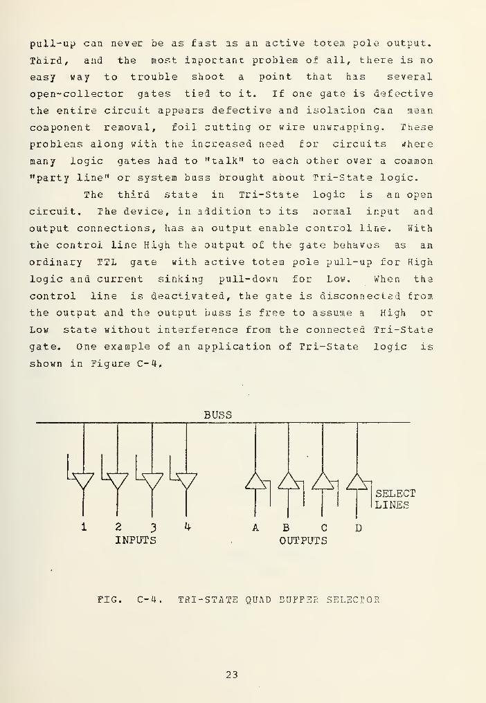
"party line" or system buss brought about Tri-State logic.
The third state in Tri-State logic is an open
circuit. The device, in addition to its normal input and
output connections, has an output enable control line. With
the control line High the output of the gate behaves as an
ordinary TTL gate with active totem pole pull-up for High
logic and current sinking pull-down for Low. When the
control line is deactivated, the gate is disconnected from
the output and the output buss is free to assume a High or
Low state without interference from the connected Tri-State
gate. One example of an application of Tri-State logic is
shown in Figure C-4.
BUSS
12 3INPUTS
WV Z^ZVAizV
B C
OUTPUTS
SELECTLINES
D
FIG. C-U. TRI-STATE QUAD BUFFER SELECTOR
23


Hare, two Tri-State quad buffers (74125) are used to select
one of four possible inputs to one of four possible outputs.
The input desired is selectively enabled as is the output.
Care must be taken to only enable one input at a time. If
more than one is enabled simultaneously the outputs are
shorted and, as with conventional TTL, damage to the IC is
almost assured.
There are presently over 15 Tri-State logic packages
to choose from in TIL as well as CMOS. While Tri-State will
not solve all design problems involving common bus
configuration, understanding its operation is an important
tool allowing a greater flexibility in digital circuit
design.
3. Laborato ry Exercises
To further increase your understanding of wired
logic, Tri-State logic and open collector output packages,
perform the following lab exercises. Prior to setting up
each circuit look up and study the device spacification
sheet in one of the company manuals [Ref. 4 ]. This simple
procedure will vastly improve your knowledge of integrated
circuits
.
a. Equipment
Analog/Digital IC Trainer
IC Breadboard
Clock Module
Switch Module
Digital circuits device manual
One each: 7400, 7403, 7404, 7406, 74125
Resistor 2.2 K ohms
b. EXCLUSIVE-OR Circuit
24

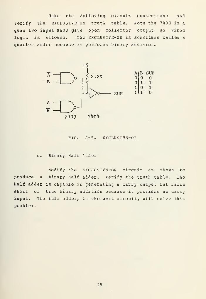
Make the following circuit connections and
verify the EXCLUSIVE-OR truth table. Note the 7403 is a
quad two input NAND gate open collector output so wired
logic is allowed. The EXCLUSIVE-OR is sometimes called a
quarter adder because it performs binary addition.
SUM
A B SUM
1 1
1 1
1 1
7^-03 7^0*4-
FIG, C-5. EXCLUSIVE-OR
c. Binary Half Mder
Modify the EXCLUSIVE-OR circuit as shown to
produce a binary half adder. Verify the truth table. The
half adder is capaole of generating a carry output but falls
short of true binary addition because it provides no carry
input. The full adder, in the next circuit, will solve this
problem.
25


SUMA B SUM CARRY
1 1
1 1
1 1 1
A
BCARRY
7403
FIG,
7404
C-6. BINARY HALF ADDER
d. Binary Full Adder
To simplify the construction of a full adder the
7486 quad EXCLUSIVE-OR gate will be used. Construct the
following circuit and complete the truth table.
SUM
Cln A B (SUMlCouti0! 1
Oi 11
10!
6 ll l i
1
I o o 1
1 01 i1
i i
i i i
CARRYOUT
7^00
FIG, C-7. BINARY FULL ADDER
2b


e. Tri-State Logic Buss Selector
Construct tie following circuit using the 7486
Tri-State quad buffer. Apply clock output "C" to point A.
By selectively enabling lines 1 thru 4, the clock output can
be routed to one or iaore places. This circuit, although
very simple, will be useful in later projects where clock
signals must be injected at various points in a circuit.
BUSS
Ai
ACLOCK
Vi Vi
X Y ZTO DISPLAY MODULE
?^86
FIG. C-8. TRI-STATE LOGIC BOSS SELECTOR
27


D. FLIP-FLOPS
1 . Lesson Ohject ives
The objectives of this lesson will be to investigate
the operation of flip-flops (FF's), starting with the basic
RS FF. Special emphasis will be placed on the clocking
action of clocked FF*s r with timing diagrams used to explain
the difference between level and edge clocking devices.
2- Discussion
a. RS Flip-Flops
A flip-flop is a binary memory device found in
computers and other sequential logic circuits. It is
bistable, which means it has two stable states and usually
has two outputs. The outputs are the complement of each
other. The simplest type of FF called a Set-Reset flip-flop
is shown in Figure D-1.
SET
R£SET
Q
Q
FIG. D-1. BASIC SET-RESET FLIP-FLOP
If both inputs are left positive, the circuit stays in the
28

original state. If the Set input is momentarily grounded,
the circuit goes to the state with Q output positive and the
"Q output grounded. If the Reset input is momentarily
grounded, the circuit goes to the state with the Q output
grounded and the ~£T output positive. When both the Set and
Reset inputs are simultaneously grounded, the flip-flop goes
into a dissallowed state condition in which the outputs are
both simultaneously positive. Since the final state cannot
be predetermined, this condition is normally avoided.
This simple circuit has several limitations
which prevent it from being commonly used. First, its
output changes immediately after application of the inputs.
1'his precludes its application in sequential circuits where
changes in the propagation delay through many flip-flops
would cause race conditions and undeterminable outputs.
Second, the device has a disallowed state when it is
instructed to Set and Reset at the same time. The two
limitations taken together preclude using the FF as a binary
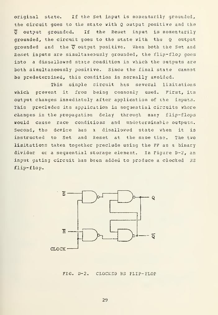
divider or a sequential storage element. In Figure D-2, an
input gating circuit has been added to produce a clocked R5
flip-flop.
CLOCK
Q
*Q
FIG. D-2. CLOCKED R3 FLIP-FLOP
29


This modification allows as to change the output only when
the input data and the clock pulse occur simultaneously.
The other problems reraaia however, and if several stages of
this circuit were cascaded together, as in a shift-register,
a critical race would occur when all the clocks
simultaneously went positive. The data would run through
all stages instead of one stage at a time. The problem
could be solved if the clock pulse duration were made less
than the propagation delay so that the data would then be
transfered only one stage at a time. While this will work,
the clock pulse width would be very critical and temperature
dependent.
b. Master-Slave Flip-Flops
To solve the race problems associated with tne
clocked RS flip-flop, the circuit of Figure D-3 is used.
MASTER SLAVE
CLOCK
FIG. D-3. MASTER-SLAVE FLIP-FLOP
Here, two clocked RS flip-flops have been cascaded with
their clock inputs driven complementary. When ths clock is
30

low, data is accepted oa the first, or master, stage. When
the clock goes high, the contents of the master stage is
transfered to the second stage, called the slave. The slave
cannot change until long after the master has completed its
changing; therefore, the possibility of a race condition is
eliminated. The Kaster-Slave type FF can be easily cascaded
to pass data, one stage at a time.
c. "T" Flip-Flo?
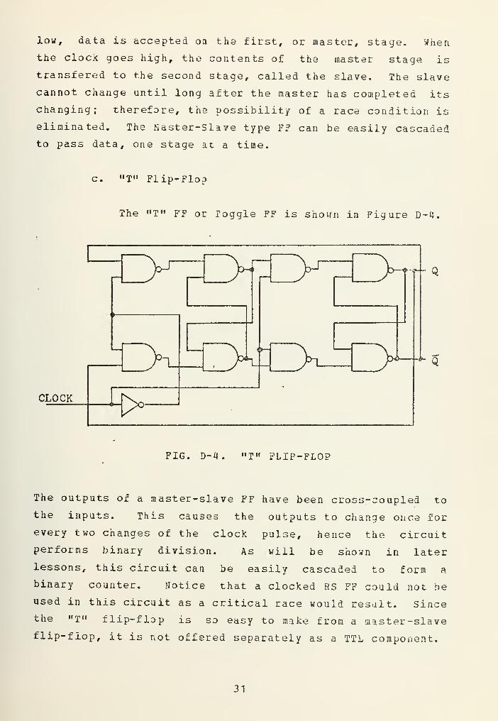
The "T" FF or Toggle FF is shown in Figure D-4.
Q
CLOCK
FIG. D-4. "T" FLIP-FLOP
The outputs of a master-slave FF have been cross-coupled to
the inputs. This causes the outputs to change once for
every two changes of the clock pulse, hence the circuit
performs binary division. As will be shown in later
lessons, this circuit can be easily cascaded to form a
binary counter. Notice that a clocked RS FF could not be
used in this circuit as a critical race would result. Sincethe "T" flip-flop is so easy to make from a master-slaveflip-flop, it is not offered separately as a TTL component.
31

d. JK Flip-Flop
The Eiaster-slave FF solved the race problem of
the ES FF; however, the problem of the disallowed input
state was not corrected. The JK FF solves this problem by
causing the flip-flop to toggle when both the J and K inputs
are high. The truth table for the 7476 JK FF is shown in
Figure D-5.
CLOCKED INPUTS:
J K CLOCK OUTPUT
~L STAYS THE SAME
1 ~L1 ~L 1
1 1 ~L CHANGES TO OPPOSITE
DIRECT INPUTS
PRESET PRECLEAR OUTPUT
DISALLOWED STATE --
DO NOT USE
1 1
1
1 1NORMALCLOCKED OPERATION
(A) Clocked inputs.
CLOCKING OCCURS WHEN CLOCK LINE GOES TO LOW LEVEL.
DATA ON J AND K LINES MAY NOT 3E CHANGED EXCEPT
IMMEDIATELY AFTER CLOCK GOES LOW. ONLY
ONE CHANGE PER CLOCK CYCLE IS PERMITTED.
(B) Direct inputs.
FIG. D-5 OPERATING RULES FOR THE 7476 FF
The 7476 is a level-triggered, JK Master-Slave FF with
preset and preclear inputs. The meaning of
"level-triggered" will be described in the following
section.
Figure D-5 shows that if both the J and K inputs
are grounded, nothing happens when the clock goes to the low
level. If the J input is made positive and the K input is
grounded, the Q output goes or stays positive when the clock
goes to the low level. The 1 on the J line is passed to the
Q output and can be thought of as the Set input of the RS
FF. If the J input is grounded and the K input is made
32


positive, the Q output goes or stays grounded when the clock
goes to the low level. The K input can be thought of as the
Reset input on the RS FF. The last possibility is when the
J and K inputs are both positive. In this case the Q output
changes when the clock goes to the low level. The circuit
acts as a "T" flip-flop or a binary divider.
The direct inputs on flip-flops are used to
clear a counting circuit to zero, or to enter a fixed number
at the begining of a counting sequence. Figure D-5 shows
that if both the Set and Clear inputs remain positive, the
FF will operate normally as just described. If only the Set
input is grounded, the FF immediately goes into the state
where Q is positive and 3 is grounded. If on the other hand
the Clear input is grounded while the Set remains positive,
the FF immediately goes into the state where Q is grounded
and Q is positive. If the Set and Clear inputs are
simultaneously grounded, a disallowed state condition
exists, where Q and Q will no longer be complementary. This
condition should be avoided. The key point to remember
about direct inputs is that they dominate all other inputs
and the clock. They effect the output immediately, and for
this reason are often refered to as asynchronous inputs.
e. Clocked-Logic
Let's digress briefly to investigate in detail
just how the clock effects the operation of clocked- logic.
There are two basic types of clocking, level and edge. In
level clocking, the state of the clock being a "0" or a "1"
carries out the operation of the FF. In edge clocking, the
change of the clock from "0" to "1", or vice versa,
completes the action.
In level-clocKed logic, if the data is allowed
to change more than once, or at random, problems can occur.
Normally, if the device is called a Master-Slave type, it is
level clocked. Figure D-6 shows a timing diagram of three
33


different types of JK FF's. All have the same clock and JK
inputs; however, the outputs are quite different.
8 9 10 11
CLOCK
JINPUT
Kj
INPUT,
POSITIVEEDGE
I
7^70,
l
I
NEGATIVEEDGE i
7^H103
MASTERSLAVE
|
7476
FIG. D-6. FLIP-FLOP TIMING DIAGRAM
The 7470 is a positive edge triggered JK flip-flop. The
timing diagram shows that it toggles only when tha J and K
information is present immediately before the clock pulse
goes Hign. During time period 2, ooth J and K inputs are
High; however, since they went low before the positive edge
34

of the clock pulse, the output did not change. The negative
edge triggered FF operates similarly as shown in the trace
of a 74H103. Because both J and K inputs are High in time
period 3, the 74H103 FF will toggle when the negative edge
of the clock occurs. Now look at the level clocked
Haster-Slave FF shown in the last trace of Figure D-6. If
we recall from our earlier description of a master-slave
device, information is transfered into the master stage
during a High level and then passed to the slave stage
during the following Low level of the clock. We see in time
period 1 that the J input is High for a fraction of the time
period. This is long enough to "load" the master and
subseguently cause the FF to toggle when the clock goes Low.
The FF was able to "ceaeraber" that the J input was High.
For this reason a very important rule should be observed
when using level-clocked logic. The rule states; "On any
level-clocked logic block, the input data cannot be changed
or altered except immediately after clocking occurs. At
that time, it can be changed only once." As a result of
this restriction, level-clocked devices should be provided
with continuous logic inputs such as hard-wired 1*s or O's.
If this is not possible the inputs should come from a source
that is clocked identically to the FF receiving theme If
the input data is continuously changing at a random rate, or
is comming from some other non-synchronous source, an
edge-triggered device should always be used for at least the
first stage. An edge-clocked logic block may have its input
data changed at any time.
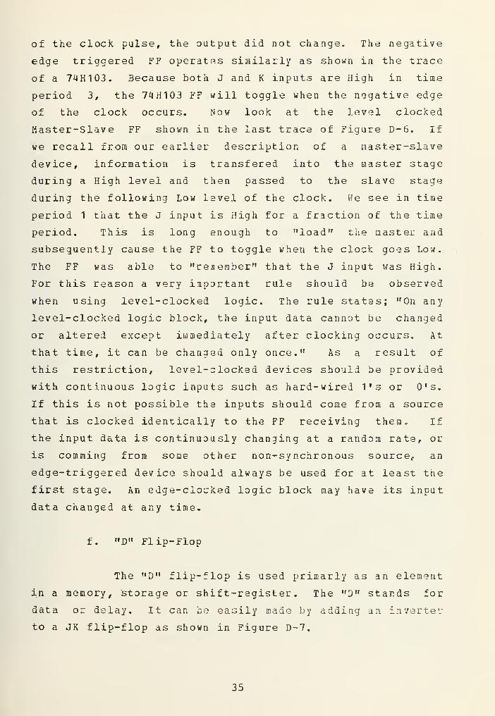
f. "D" Flip-Flop
The "D" flip-flop is used primarly as an element
in a memory, storage or shift-register. The "D" stands for
data or delay. It can be easily made by adding an inverter
to a JK flip-flop as shown in Figure D-7.
35

CLOCK
Q
— Q
FIG. D-7 "D" FLIP-FLOP
The K input is always the complement of the J, thus only one
input is needed. If the "D" input is positive, the Q output
goes or stays positive when the clock changes. If the "D"
input is grounded, the Q output goes or stays grounded when
the clock changes. "D" FF's are normally edge- triggered
devices and are available in pairs in the 7474, or in
quadruplicate in the 74175, and by sixes in the 74174.
3. l§;k2£§J.orY Exercises
Since the FF is such a basic building block of
digital circuits, it is offered in many IC package formats
that give the designer the choice of the type of FF, method
of clocking, pinout, and the number of FF's per package.
FF's will be used extensively in the following lab
exercises, so the actual connection of FF circuits will be
delayed until then. In preparation for those exercises, the
following exercise should be performed.
Using an IC Circuits Manual as a reference source,
construct a table of information for the 7400 series of IC
FF's. Label the columns with the device number, starting
with the four most common FF's; 7473, 7474, 7476 and 74107.
36

Label the remaining coluans 7470, 7472, 74104, 74105, 74110,
and 74111. The rows of the table should be labeled as
follows: Type (JK, D, etc.), Clocking, Supply pinouts
(standard or non-standard), Package (14 or 16 ), Devices per
package. Direct set (yes or no) , Direct clear (yes or no) ,
Restrictions (on input changes, etc) , rtax frequency and
Power consumption. You will learn a great deal as you
compile this table, and additionally it will serve as a
ready reference for future lab axercises and design work.
37

E. ASYNCHRONOUS COUNTERS
1. Lesson Objectives
This lesson will discuss the advantages and
disadvantages of asynchronous counters and several examples
of asynchronous modulo counters will be described. The
construction of counter circuits using medium scale
integration (KSI) IC packages will be explained in detail.
2. Discussion
Asynchronous counters, also known as ripple or
serial counters, use the output of a counting element to
drive the input of the following counting element. The
elements most often used are flip-flops (FF's) operating in
the toggle mode, which means they change state with each
clock pulse. Generally speaking, ripple counters require
less external gating to perform a desired function as
compared to synchronous types. The main disadvantage of
ripple counters is that the propagation delays through the
individual elements are additive. This means that the last
element in a long high-speed counter is considerably out of
phase with the input of the first stage. For example,
consider a counter operating at 20 MHZ and using 10 FF's of
the 7476 type. The typical propagation delay per element is
listed as 25 nano-seconds (ns) . The time required for the
input pulse tc propagate to the output is 250 ns, yet there
is only 50 ns between input pulses. During this ripple or
settling time, any intermediate states will be invalid. In
spite of this problem, ripple counters are very useful for
straight frequency division, and are excellent for
high-speed counting that must be read out after the count is
completed.
Flip-flops were discussed in detail in the previous
lesson, including the difference between positive-level
38

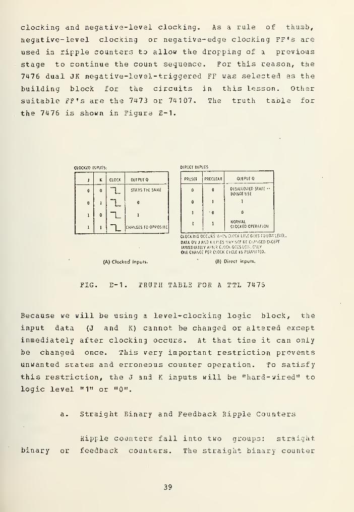
clocking and negative-level clocking. As a rule of thumb,
negative-level clocking or negative-edge clocking FF's are
used in ripple counters to allow the dropping of a previous
stage to continue the count sequence. For this reason, tne
7476 dual JK negative-level-triggered FF was selected as the
building block for the circuits in this lesson. Other
suitable FF's are the 7473 or 74107. The truth table for
the 7476 is shown in Figure E-1.
CLOCKED I NPUTS
i K CLOCK OUTPUT
~L STAYS THE SAME
1 ~L1 "L 1
1 1 ~L CHANCES TO OPPOSITE
DIRECT INPUTS
PRESET PRECUAR OUTPUT Q
DISALLOWED STATE -L'ONOr USE
1 !
1•
1 1NORMALCLOCKED OPERATION
(A) Clocked inputs.
CLOCKING OCCURS IVHEN CLOCK LINE GOES TO LOW LEVEL.
DATA ON J AND K L INES MAY NOT BE CHANGED EXCEPT
IMMEDIATELY AFTER CLOCK GOES LOW. ONLY
ONE CHANGE PER CLOCK OGLE IS PERMUTED.
(B) Direct inputs.
FIG. E-1. TRUTH TABLE FOR A TTL 7475
Because we will be using a level-^clocking logic block, the
input data (J and K) cannot be changed or altered except
immediately after clocking occurs. At that time it can only
be changed once. This very important restriction prevents
unwanted states and erroneous counter operation. To satisfy
this restriction, the J ani K inputs will be "hard-wired" to
logic level "1" or "0".
a. Straight Binary and Feedback Ripple Counters
Sipple counters fall into two groups: straight
binary or feedback counters. The straight binary counter
39


divides the input by 2 , where n is the number of elements
or FF's. The 3 outputs of each FF represent a natural
binary number with the first FF representing the least
significant figure. There is no limit to the number of FF's
that can be added. Figure E-2 shows a four element straight
binary ripple counter. Note that the J and K inputs are
hard wired to logic level "1" which forces the FF to toggle
each time the clock drops to a "0" level. The hard wiring
of the inputs also prevents changes which could cause
erroneous operation. The preset and clear lines are also
maintained at logic leveL "1" in accordance with the 7476
truth table of Figure S-1.ABCit 1 ii
CLKIN
j q|_,, ,—
j
K K <5
4 6 J Q
I
NOTE: Direct Pet and Clear connected High.All FF' s 7^4-76
COUNT SEQUENCE TABLE
A B C D iDecimall! 4 3 C D Decimal1 8
10 1 10 1 910 2 10 1 10
110 3 110 1 1110 1* 11 12
10 10 5 10 11 13110 6 111 14
1110 7 1111 15
FIG, E-2 STRAIGHT BINARY RIPPLE COUNTER
This is a four bit binar/ counter which will divide tne
input pulse stream by 16. The natural binary numbers
produced L»y this counter are rather difficult to handle and
decode, so the counter is modified into another form using
40


feedback. The feedback counter or modulo counter will count
to a certain programed number, and then reset, stop or
recycle itself automatically. The modulo of a counter is
simply how many states the counter goes through before
repeating. A decade counter has a modulo of ten. Figure
E-3 shows a typical feedback counter. The count sequence
table shows that the feedback provides for a count in binary
coded decimal (BCD) format.
B
CLKIN
" 1
"
f J Q
C
K "Q
n -J Q
-C
K Q
CLEAR
J Q
C
—e <
K Q
J QC
K ~Q
7^00
NOTE: Direct Set connected High.All FF's ?^-?6
Count Sequence Tcble
A B c D Decimal
i o 1
1 2
I 1 3
1 4
1 1 5
1 1 6
1 1 1 7
1 8
1 1 9
FIG. E-3. FEED3ACK RIPPLE BCD COUNTER
b. Directional Counters
The counters described so far are up-only
41


counters; they count only in a direction of increasing
states. When a backward-counting sequence is desired a
straight binary counter, as that shown in Figure E-2, can be
modified by taking the complement of the outputs (frora~Q) to
give a decreasing state with each count. Notice that this
is not possible with a feedback binary counter such as the
BCD counter of Figure E-3. This counter normally counts
from to 9. Complement the output and it counts from 15
down to 6; not 9 down to 0.
c. TTL MSI Counters
The counters used as examples thus far have been
made up from discrete IC FF's and gates resulting in
multiple package counters. As IC technology advanced, it
became possible to fabricate entire counters in one MSI
package. The 7490 shown in Figure E-4 is an example of a
one package counter.
TOP VIEW
FIG. E-4. TTL 7490 COUNTER
42


This is a ripple decade counter that consists of four
master-slave FF's internally interconnected to provide a
divide-"by two or a divide-by five counter. By externally
connecting the Q1 output to the Clock. 2 input, the FF's are
interconnected to give a ripple BCD-up direction counter.
The input pulse stream is applied to the Clock 1 input and
the BCD output is taken at Q1 , Q2, Q4, and Q8. The counter
is reset to "0" by bringing both 0-Set inputs high. Inputs
are also provided to reset a BCD 9 count for nine's
complement decimal applications. It should be noted that
all the 0-Set and 9-Set inputs must be grounded for normal
counting operation. For multiple-decade operation this
counter may be cascaded oy connecting the Q8 output of the
first stage to the Clock 1 input of the next. At first this
connection may seem in error since the Q8 output is high for
the count of 8 and 9. However, since the 7490 is a negative
edge clocking unit, the pulse will only trigger the next
decade when the present count goes from 9 to 0.
Other one package asynchronous counters
avaiiiable include the 7492, 7493, and the 74142. All these
counters have typical clocking rates of 18 MHZ and, as the
lao exercises will show, they drastically reduce the
interconnections necessary to realize a multiple decade
counting circuit.
3* Laboratory Exercises
To further increase your understanding of
asynchronous counters, perform the following lab exercises.
Prior to setting up each circuit, look up and study the
device specification sheet in one of the company manuals.
This simple procedure will vastly improve your knowledge of
integrated circuits.
43


a. Equipment
Analog/Digital IC Trainer
IC Breadboard
Clock Module
Binary Display Module
Numerical Display Module
Digital circuits device manual
One each: 7400
Two each: 7476,7490
b. Four-Bit Binary Counter
Make the circuit connections for the 4-bit
binary counter shown in Figure E-2. Connect the outputs of
FF's A through D to the Binary Display Module and use the
manual push button on the Clock Module as a clocking source
for the counter. By operating the push button, verify the
truth table of Figure E-2. Do not confuse the Clear input
of the 7476 with the Clock input. Both the Clear and Set
inputs may be left unconnected, but it is good engineering
practice to connect them High. When the Clear input is
grounded the FF will immediately go into the state with Q
Low and Q High, Grounding the Set input will give the
opposite results. Test the operation of these functions.
Note that the Set and Clear inputs snould never be
simultaneously grounded, as a disallowed state will result.
c. BCD Asynchronous Counter
Modify the 4-bit binary counter to realize the
BCD counter of Figure E-3. Operate the push button on the
Clock Module and verify the truth table. By using the
proper feedback, you should be able to convert this counter
into any modulo number fron 1 to 10. Try it.
44


a. TTL MSI Counters
Using the manufactures data sheet and Figure E-4
as a guile, make a connection diagram of a two decade BCD
counter using two cascaded 7490 counters. 3uild the circuit
and verify its proper operation. Also check the operation
of the 0-Set and 9-Set inputs. Replace the 3inary Display
Module with the Numerical Display Module and verify the
proper operation of the counter and display.
45


F. SYNCHRONOUS COUNTERS
1 • Lesson Object iv es
This lesson ifill discuss the advantages and
disadvantages of synchronous counters, and several examples
of synchronous modulo counters will be described. The
benefits of combining synchronous and asynchronous elements
in counter design will also be explained. Additionally,
medium scale integration (MSI) IC package counters will be
described in detail with a decade counter used as an
example.
2 • Discussion
A synchronous counter is one in which each element
or flip-flop (FF) is clocked in parallel and ail state
changes occur simultaneously with the clock pulse. Since
all FF's change simultaneously, the output of a synchronous
counter can be taken in parallel form as opposed to serial
form for ripple counters. Because the clocking action is
not additively delayed, it is easy to interface this type of
counter with other circuits that are synchronized with the
system clock. This is the primary advantage of a
synchronous counter. Some disadvantages are: the clock must
have a fan out capable of supplying the many FF's that would
be necessary in a long chain counter. Additionally, all the
FF's must be capable of toggling at the maximum frequency
expected. In a ripple counter this was not necessary as
only the first stage was exposed to the maximum input
freguency. As with other engineering trade-offs, the
advantages and disadvantages must be weighed on a case basis
and the proper counter selected. Synchronous counters can
be made to count up, down, or be switch selectable up or
down.
46


a. Modulo-4 Synchronous counter
The simplest type of synchronous counter is the
modulo type, where an input pulse stream is divided an
integer number of times. A good example is the nodulo-4
counter shown in Figure F-1.
|| 4 ||
i L B
.
—
J <4
l
J (41
r% c
J Q J Q
LK_j
—
Counts B A
1 1
2 1
3 1 1
h
IN
NOTE: Direct Set and Clear connected High.
All FF's 7^76
FIG, F-1. M0DUL0-4 COUNTER
This is immediately recognized as a synchronous counter by
the fundamental property of parallel driven clock inputs.
FF A has the J and K terminals hard-wired to logic "1 f1.
This will cause it to toggle with each clock pulse. Since
its output Q is tied directly to the J and K inputs of FF 3,
it will cause B to toggle on every second pulse. The result
is a counter which counts from 00 to 11, and then resets to
00, as shown in the truth table. One restriction in using
level clocking FF' s is that the input data cannot be changed
or altered except immediately after clocking. At that time
it can be changed only once. This restriction is satisfied
in the counter shown in Figure F-1 since the input to FF B
47

will never change mora than once per clock pulse and then
normally within 25 nano-seconds (ns) of clocking. The 25 ns
accounts for the manufacture's listed propagation time for
the 7476 FF's used in this counter.
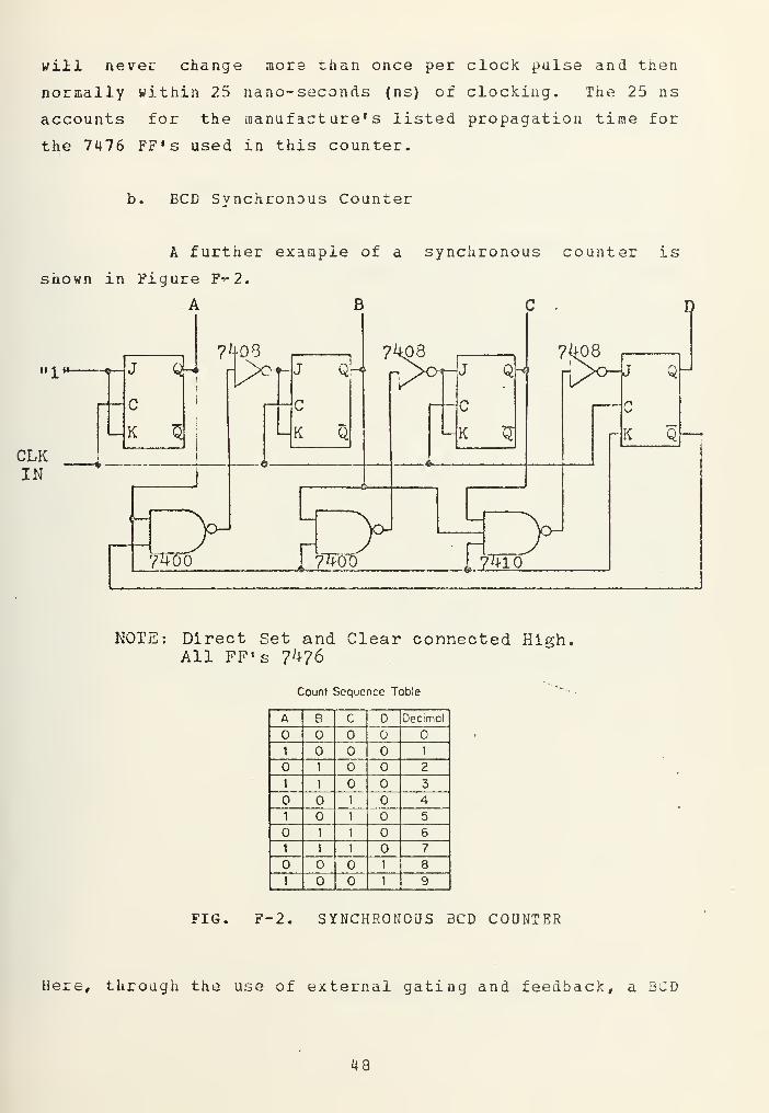
b. BCD Svnchronous Counter
A further example of a synchronous counter is
shown in Figure F^2.
CLKIN
|| ^H <v J
C
K
V
~t
7400
08
I
B
J Qh'
K Q
7^08J Q
C
K $
7^00 U2MQ
7ft08
rlyo- J Q
K Q
P
NOTE: Direct Set and Clear connected High.All FF's 7^76
Counl Sequence Table
A B c D Decimal
O1 1
1 2
1 1 3
1 4
1 1 5
1 1 6
1 1 1 7
1 8
1 1 9
FIG. F-2. SYNCHRONOUS BCD COUNTER
Here, through the use of external gating and feedback, a BCD
48


or decade counter is realized. The output of the counter is
taken directly off the Q terminals of the FF's with A being
the least significant bit. The truth table shows that the
counter will reset to 0000 every ten clock pulses.
c. Combination Synchronous Asynchronous Counter
As the modulo number of the counter increases
the number of external gates required to realize the counter
also increases rapidly. To alleviate this problem, a
combination synchronous asynchronous circuit is used.
Figure F-3 shows an example of a combination BCD counter.
ii 1 it
CLKIN
NOTE: Direct Set and Clear connected High.All FF's 7^76
Count Sequence Table
A B c D Decimal
1 1
1 2
1 1 3
1 4
1 1 5
1 1 6
1 1 1 7
1 8
11 9
FIG. F-3. :0MBIN ATION BCD COUNTER
49

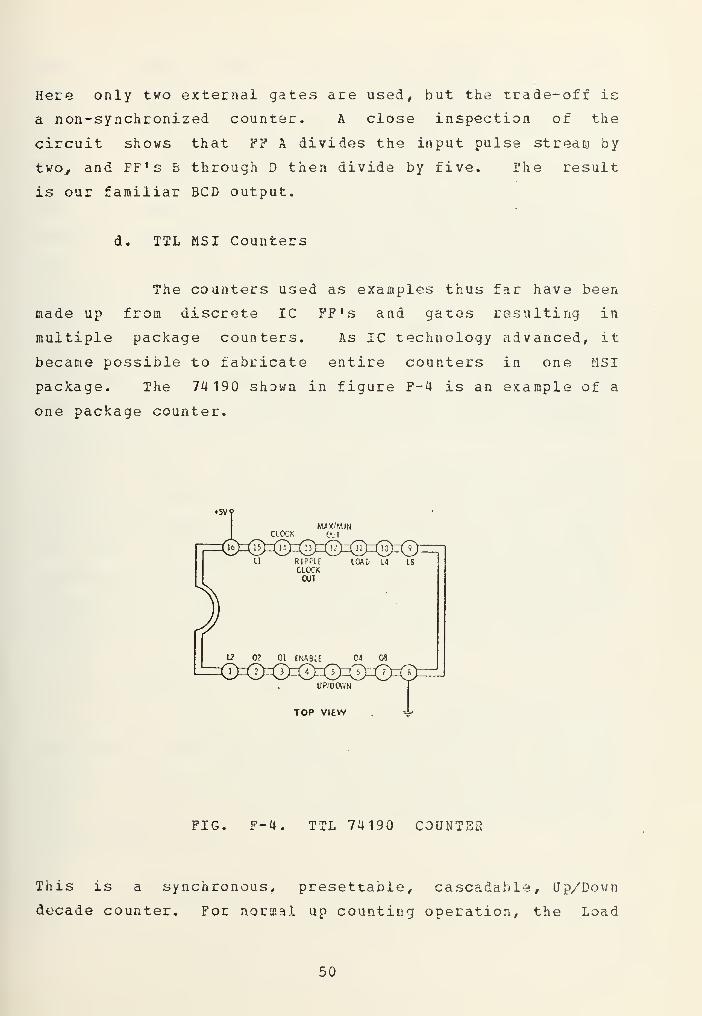
Here only two external gates are used, but the trade-off is
a non-synchronized counter. A close inspection of the
circuit shows that FF A divides the input pulse stream by
twov and FF's b through D then divide by five. The result
is our familiar BCD output.
d. TTL MSI Counters
The counters used as examples thus far have been
made up from discrete IC FF's and gates resulting in
multiple package counters. As IC technology advanced, it
became possible to fabricate entire counters in one MSI
package. The 74 190 shown in figure F-4 is an example of a
one package counter.
I? 0? 01 ENABLE
UP/DOWN
TOP VIEW
FIG. F-4. TTL 74190 COUNTED
This is a synchronous, presettable, cascadable, Up/Down
decade counter. For normal up counting operation, the Load
50

should be High, Enable and Up/Down should be Low. The
counter advances one count synchronously on each
ground-to-positive transition of the input clock. The BCD
output is taken at Q1, Q2, Q4, and Q8 . To preset the
counter, a number is loaded in parallel on the load inputs
L1, L2 e L4, and L8 # and the Load input is briefly brought
Low. Since there is no separate Clear input, the counter is
cleared by loading all zeros. To count down, the Up/Down
input is made High. For fully synchronous multiple decade
operation, the Ripple Clock Output of the first stage is
connected to the Enable of the second. All stages are
synchronously driven from the input clock. The
maximum/minimum count output can be used to accomplish
look-ahead for high speed operation. It produces a high
level output pulse with a duration approximately equal to
one complete cycle of the clock when the counter overflows
or underflows.
Other one package synchronous counters
availiabie include the 74160, 74192, 74161 and 74191. The
last two are known as 4 bit binary counters as they divide
the input by sixteen. All these counters have typical
clocking rates of 20 MHZ, and as the lab exercises will
clearly show, they drastically reduce the interconnections
necessary to realize a multiple decade counting circuit.
3« L2;22=Latorv Exercises
To further increase your understanding of
synchronous counters, perform the following lab exercises.
Prior to setting up each circuit, look up and study the
device specification sheet in one of the company manuals.
This simple procedure will vastly improve your knowledga of
integrated circuits.
a. Equipment
51

Analog/Digital IC Trainer
IC Breadboard
Clock Module
Binary Display Module
Numerical Display Module
Digital circuits device manual
One each: 7400,7404,74 10
Two each: 7476, 74190
b. Modulo-4 Synchronous Counter
Make the circuit connections for the modulo-4
counter shown in Figure F-1. Connect the outputs of FF's A
and B to the Binary Display Module and use the manual push
button on the Clock Module as a clocking source for the
counter. By operating the push button, verify the truth
table of Figure F-1.
c. BCD Synchronous Counter
Modify the modulo-4 counter to realize the BCD
counter of Figure F-2. Make the necessary additional
connections from FF's C and D to the Binary Display Module.
Operate the push button on the Clock Module and verify the
truth table of Figure F-2.
d. Combination Synchronous Asynchronous Counter
Modify the synchronous BCD counter to realize
the combinational BCD counter of Figure F-3 and verify the
truth table.
e. TTL MSI Counters
Using the manufactures data sheet and Figure F-4
as a guide, make a connection diagram of a two decade
52


counter using two cascaded 74190 counters. Build the
circuit and verify its proper operation. Check the proper
operation of the Up/Down modes. Replace the Binary Display
Module with the Numerical Display Module and verify the
proper operation of the counter and display.
53

G. SHIFT REGISTERS
1 . Lesson Objectives
Shift registers are an integral part of every
computer. They are also used extensively to interface data
between various binary devices. This lesson will describe
their operating characteristics and provide some examples to
aid in the understanding of these versatile devices.
2- Discussion
A shift register is a group of two or more
flip-flops cascaded together and wired so as to allow the
contents of all stages to be shifted one stage at a time in
the desired direction. Some of the more important uses of
shift registers are to store information, to form counters
or frequency dividers, and to convert data from parallel
form to serial form and vice versa. They are classified
according to three basic considerations: their method of
data handling (serial-in serial-out, serial-in parallel-out,
parallel-in serial-out, parallel-in parallel-out) , their
direction of data movement, (shift right, shift left,
bidirectional), and their bit length.
a. Basic Shift Register Classifications
The form in which data is entered and removed
from a group of FF's determines the type designation of the
register. The most basic of the four possible forms is the
serial-in serial-out (SI50) , shown in Figure G-1.
54


SERIAL o-
IN
aoa o-
c
D o
c c
D U
c
-oMKi/U
FIG. G-1. SERIAL-IN SERIAL-OUT SHIFT REGISTER
Here, four D flip-flops are cascaded to form a 4-bit
sequential memory that accepts one bit of information per
stage. Since the FF ' s are cascaded, the information is
passed on in order of entry, and the first bit in is the
first bit out. A SISO register can be used to provide a
buffer between systems with different clock rates. It is
also used as a delay. Data at the input is delayed a total
of n clock pulses, where n is the length of the register.
This delay feature will be used later in this lesson to form
a counter.
A serial-in parallel-out (SIPO) register is
shown in Figure G-2.
SERIAL o-IN
CLOCK o-
?A OUTPUT
c
D
C
?B OUTPUT
r D Q
C
?C OUTPUT
D Q
C
?D OUTPUT
FIG. G-2, SERIAL-IN PARALLEL-OUT SHIFT RE3ISTSR
Here, the serial data that is entered can be read out at
each register stage. This is the primary purpose of this
type of register as many arithmetic functions in a computer
are performed on "words" in parallel form.
To convert a word from parallel form to serial
form, a parallel-in serial-out (PISO) register is used.
This type circuit is shown in Figure G-3.
55

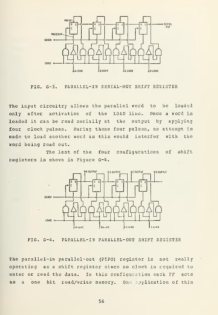
PfUStT
601OA0
FIG. G-3. PARALLEL-IN SERIAL-OUT SHIFT REGISTER
The input circuitry allows the parallel word to be loaded
only after activation of the LOAD line. Once a word is
loaded it can be read serially at the output by applying
four clock pulses. During these four pulses, no attempt is
made to load another word as this would interfer with the
word being read out.
The last of the four configurations of shift
registers is shown in Figure G-4.
aoa o-
10AD cv-
o o
c
PA OUTPUT 08 OUTPUT ?C OUTPUT ?D OUTPUT
I<r—' o
c
<—
I
D
C c
—I i 1—I—
J
1
—
I—
J
1
—
I— I
ktvK) ItUAD I I. 10*0 1 DtOO
FIG. G-4. PARALLEL-IN PARALLEL-OUT SHIFT REGISTER
The parallel-in parallel-out (PIPO) register is not really
operating as a shift register since no clock is required to
enter or read the data. In this configuration ea~h FF acts
as a one bit read/write memory. On--, pplication of this
56


circuit would be a holding register where a parallel word
may be temporarily stored for use at a later time.
Because of their importance in digital
electronics, shift registers are availiable as complete
integrated circuit packages as opposed to building up
circuits from discrete flip-flops. Most of thesa registers
shift only to the rignt, while some shift only to the left.
This means they are only capable of moving data in one
direction. A few registers are made that shift in either
direction on command. These registers, called
bidirectional, have separate clock, shift-left and
shift-right busses.
The last form of classification is ths number of
bits per IC package. For example, a 16 bit shift register
can be made by cascading two 8 bit shift register IC's. The
number of bits that can be put into one IC package is
limited by the number of pins needed to interconnect them to
the outside world. A SISO register needs only ons input and
one output pin for the data, so a register with sight bits
is availiable. For a SIPO register capable of bilirectional
control, a pin is needed for the output of each stage as
well as the control functions. This large number of
external connections limits the 16 pin package to four bits.
Figure G-5 shows a brief summary of some of the more popular
shift registers that are availiable.
Parallel
Typo length Out? Parallel Load? Direction Clear
7491 8 Bits No No Right No7494 4 Bits No Pre-sef only Right Yes
7495 4 Bits Yes Synchronous Right/left No7496 5 Bits Yes Preset only Right Yes
74164 8 Bits Yes No Right Yes
74165 8 Bits No Yes Right Yes
74166 8 Bits No Synchronous Right Yes
74194 4 Bits Yes Synchronous Right/left Yes
74)95 4 Bits Yes Synchronous Right Yes
FIG. G-5. SEVERAL TTL SHIFT REGISTERS
57


b. Shift Counters
Since each stage of a shift register acts as a
one bit memory, it can be interconnected to form a counter.
Shift counters are a specialized form of clocked counters.
In general, the shift counter results in outputs that may
easily be decoded, and normally they require no gating
between stages. A simple inodulo-4 counter is made from a 4
bit register as shown in Figure G-6.
CLOCK
A
!
B
1
C DA
D Q
C
D Q
C
D Q
C
D Q
C
. o i »
—
1 »
—
1
FIG. G-6- M0DUL0-4 COUNTER
If a "1" is loaded into the first stage , it will take four
clock pulses to appear at the output. Since the Q output of
the last stage is fed back to the input, the process repeats
indefinitely. Note that a decade counter would take ten
stages. This is not an efficient way to make a decade
counter, however, no decoding of the output is necessary. A
slight modification of the circuit is made, as shown in
Figure G-7, to produce a Johnson counter or a switchtail
ring counter.
53


CLOCK
FIG. G-7. JOHNSON COUNTER
Here, the complement of the last stage is fed back to the
input so that with every colcking, the first stage becomes
whatever the last stage was not on the previous clock pulse.
If we start with the register at 0000, the next clock pulse
will produce a 1000, followed by 1100, 1110, 1111 etc. It
will take eight clock pulses to return to the initial state
of 0000, so we now have a modulo-8 counter. Note that only
one output changes for any clock pulse. This will eliminate
any race problems on decoding.
A major problem associated with shift counters
is that of disallowed states. In any counting system made
up of n binary storage stages, the total different possible
stated is 2 . The counter of Figure G-7 has four stages or
16 possible states. Since it is a modulo-8 counter, only
half of the possible states are used. If one stage should
mistrigger, and the wrong bit sequence should become
present, the counter would continue to circulate the wrong
code until preset and corrected. This problem can be
overcome by the inclusion of automatic presetting or
error-correcting logic.
c. Pseudo-fiandon Binary Sequence Generator
59


Frequently the need arises for a completely
random stream of bits. A serial-in parallel-out shift
register can be interconnected with one Exclusive OR gate,
as shown in Figure G-8, to produce a pseudo-randota sequence
generator.
CLOCK 7^86
FIG. G-8. FOUR 3IT PSEUDO-RANDOM SEQUENCER
The output of this generator will be random but, will repeat
every 2 -1 bits, where n equals the number of flip-flops
used in the shift register. For the circuit of Figure G-8,
the output will repeat after 31 clock pulses. If n is
large, the output will appear to be completely random. As
an example, the Word and Random Number Generator Module has
the equivalent of a 60 bit shift register. If this
pseudo-random generator is clocked at the 1 MHZ rate, the
output will repeat every 365 centuries - truly random.
Since there are 2 possible states in any given
combination of binary memory devices, four shift registers
should give 32 states. In the circuit of Figure G-8, there
is one disallowed state. A close look at the circuit will
show that this disallowed state is 0000.
60


3. Laboratory Exercises
To further increase your understanding of shift
registers, perform the following lab exercises. Prior to
setting up each circuit, look up and study the device
specification sheet in one of the company manuals. This
simple procedure will vastly improve your knowledge of
integrated circuits.
a. Eguipment
Analog/Digital IC Trainer
IC Breadboard
Clock Module
Binary Display Module
Numerical Display Module
One each: 74175,7486
b. Shift Counters and Pseudo-Random Sequencers
Make the circuit connections for the modulo-
4
counter, shown in Figure 3-6, using one quadruple D-type FF
(74175). Connect the outputs of the FF's to the Binary
Display Module and the clock input to the Clock Module.
Load a "1" into the first FF and operate the push button on
the Clock Module to verify the proper operation of the
circuit. Ensure that the clear input on the 74 175 is
connected High.
Modify the counter to realize the modulo-8
counter circuit of Figure G-7 and verify its proper
operation.
Modify the circuit to realize the 4-bit
pseudo-random sequencer shown in Figure G-Q. Connect the
outputs of the four FF's to one decade of the Numerical
61

Display Module. Clear the register and load a "1" in the
first stage. Clock the register and record the output after
each clock pulse. Verify that the sequence repeats after 31
clock pulses. Load all zeros into the register and observe
the results.
As a final exercise, look up each of the shift
registers outlined in Figure G-5 and compare their features.
Expand the table to include more of their features, such as
clocking rate, number of pins etc.
62

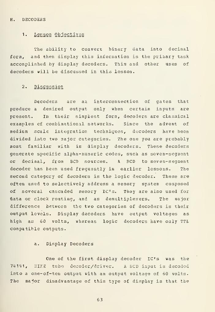
H. DECODERS
1 . Lesson Objectives
The ability to convert binary data into decimal
form, and then display this information is the primary task
accomplished by display decoders. This and other uses of
decoders will be discussed in this lesson.
2« Discussion
Decoders are an interconnection of gates that
produce a desired output only when certain inputs are
present. In their simplest form, decoders are classical
examples cf combinational networks. Since the advent of
medium scale integration techniques, decoders have been
divided into two major categories. The one you are probably
most familiar with is display decoders. These decoders
generate specific alpha-numeric codes, such as seven-segment
or decimal, from BCD sources. A BCD to seven-segment
decoder has been used frequently in earlier lessons. The
second category of decoders is the logic decoder. These are
often used to selectively address a memory system composed
of several cascaded memory ICs. They are also used for
data or clock routing, and as demultiplexers. The major
difference between the two categories of decoders is their
output levels. Display decoders have output voltages as
high as 60 volts, whereas logic decoders have only TTL
compatible outputs.
a. Display Decoders
One of the first display decoder ICs was the
74V41, IIIXE tube decoder/driver. A BCD input is decoded
into a one-of-ten output with an output voltage of 60 volts.
The major disadvantage of this type of display is that the
6 3


numbers within the tube are not on the same plane.
Additionally, they were rather fragile, consumed a lot of
power and were large in size.
With the advent of the light emitting diode
(LED) , seven-segment decoders and displays have become
popular. Here a BCD input is decoded to one-of-seven to
drive the seven segments of the display. The LED display as
well as the decoder are available in either a common-anode
or common-cathode configuration. The common-anode decoder
can only be used with a common-anode LED display. The same
is true for the common-cathode configuration. LED's are
basically diodes with a forward voltage drop of
approximately 1.7 volts. Since they are current-operated
devices, some means must be provided to limit their current
when they are operated on +5 volts. Current limiting
resistors are used between the decoder and the LSD display
to limit the current to 10-20 raA per segment. For a 20 mA
segment current, a standard value resistor of 180 ohms is
used as shown in Figure H-1.
+5 V
180 ohms
8 4 2 1 BCD
FIG. H-1. SEVEN SEGMENT DECODER/DRIVER AND DISPLAY
64

Since the maximum allowable current and forward voltage vary
somewhat between manufactures, refer to the data sheet of
the particular display for specific values. The value of
the current limiting resistor is found by subtracting the
forward voltage drop from 5 volts and then dividing by the
nominal current per segment.
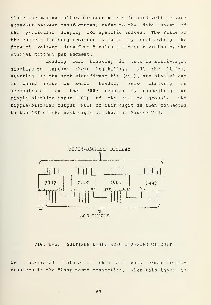
Leading zero blanking is used in multi-digit
displays to improve their legibility. All the digits,
starting at the most significant bit (MSB) , are blanked out
if their value is zero. Leading zero blanking is
accomplished on the 7447 decoder by connecting the
ripple-blanking input (RBI) of the MSB to ground. The
ripple-blanking output (RBO) of this digit is then connected
to the RBI of the next digit as shown in Figure H-2.
SEVEN-SEGMENT DISPLAY
mini ||1
llll III1
1
III
7^7A9I p.po
7^7R8I Rpo
74^-7 7447R8I
V_
|_
1
1
~
;
JBCD INPUTS
FIG. H-2. MULTIPLE DIGIT ZERO BLANKING CIRCUIT
One additional feature of this and many otaer display
decoders is the "lamp test" connection. When this input is
65

grounded, all seven segments will light regardless of the
state of any other input.
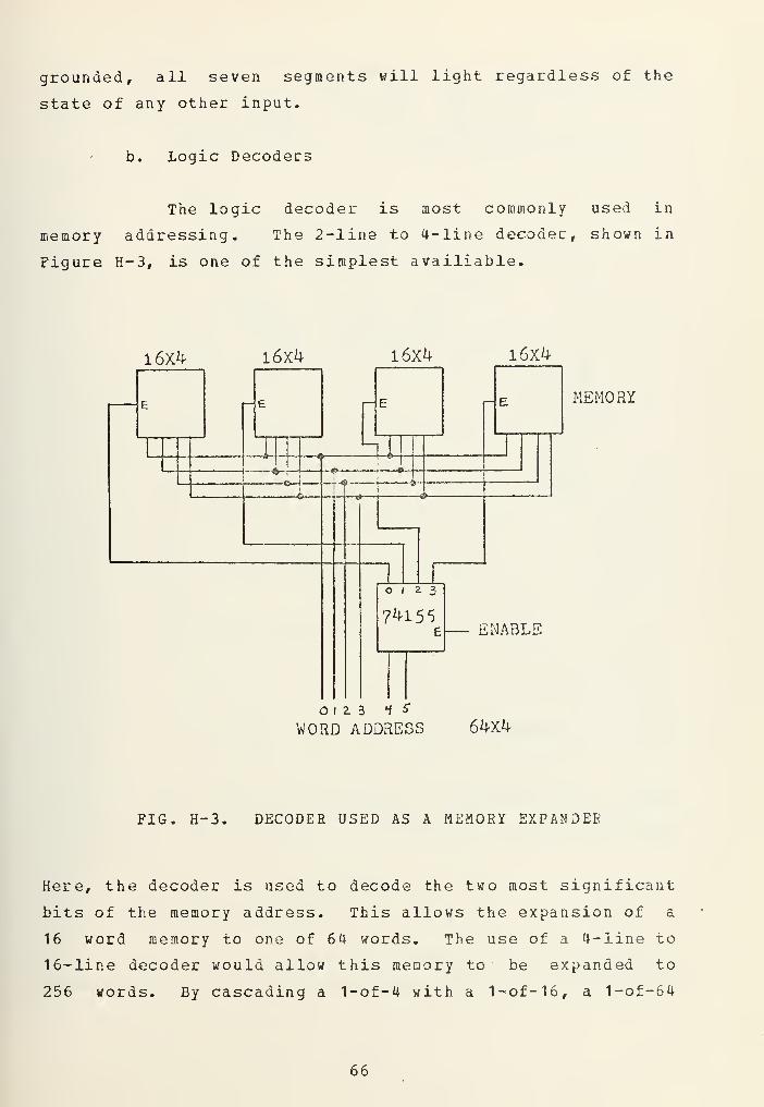
b. Logic Decoders
The logic decoder is most commonly used in
memory addressing. The 2-line to 4-line decoder, shown in
Figure H-3, is one of the simplest availiable.
16x4 16x4 16x4
O 1 Z 3 H S
WORD ADDRESS
16x4
MEMORY
ENABLE
64x4
FIG. H-3. DECODER USED AS A MEMORY EXPANDER
Here, the decoder is used to decode the two most significant
bits of the memory address. This allows the expansion of a
16 word memory to one of 64 words. The use of a 4-line to
16-line decoder would allow this memory to be expanded to
256 words. By cascading a 1-of-4 with a 1-of-16, a 1-of-64
66


decoder could be made which could then be used to further
expand this memory to 1024 words. One can easily see the
great power of the decoder in memory expansion.
Another use of a 1-of-4 decoder is shown in
Figure H-4.
CLOCK-
CLOCK
h
fa
h
04
*A%%
FIG. H-4. FOUR PHASE CLOCK GENERATOR
Here, a four phase clock signal is achieved from a single
phase source. The output of the generator is non-overlaping
TTL pulses.
3. Laboratory Exercises
To further increase your understanding of decoders,
perform the following lab exercises. Prior to setting up
67


each circuit, look up and study the device specification
sheet in one of the company manuals. This simple procedure
will vastly improve your knowledge of integrated circuits.
a. Equipment
Analog/Digital IC Trainer
IC Breadboard
Clock Module
Switch Module
Binary Display/Logic Probe Module
Digital Circuits Device Manual
One each: 7476, 74155
b. Logic Decoders
Connect one 74 155 2-line to 4-line decoder as a
memory expander. Use the Switch Module to actuate the six
word address lines. Substitute the Binary Display/Logic
Probe Module for the memory. By observing the light
display, verify the ability of the circuit to properly
address all 64 memory locations.
Modify the circuit as necessary to produce the
four phase clock generatar shown in Figure H-4. Connect the
outputs of the individual phases to the Binary Display/Logic
Probe Module and verify the proper operation of the circuit.
68


I. OP-AMP CiRCUT DESIGN
1 . Lesson Objectives
The large number of different op-amps availiable
today has compounded the problem of selecting the proper
op-amp to provide optimum circuit performance. The problem
seems to be further aggravated by lengthy data sheets
containing two to four pages of statistics and graphs. The
objectives of this lesson will be two fold: first, to review
the most important parameters found in op-amp data sheets
and second, to formulate a systematic procedure to be used
in selecting the proper op-amp for the specific design
problem. This selection procedure will be applied to
example problems in the design of inverting and
non-inverting amplifiers as done in Reference 5.
2 • Discussion
a. Open Loop Voltage Gain
Open loop voltage gain (Avol or Aol) is defined
as the ratio of the change in output voltage to the change
in input voltage. It is highly frequency dependent as shown
in Figure 1-1. The equation used frequently to determine
the closed loop gain of an inverting amplifier is shown
along with the amplifier configuration in Figure 1-2.
69

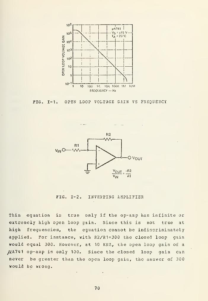
106
105
z< ,
uio2 103_i
oi 102ooJ 10zUia.
io-i
1
'1
pA741 1
N TA = 25'C
j
|
I i NJ: i
'
l
i
i
i !
!
N.
1
I !
i j\
1 10 100 IK 10.< 100K 1M 10M
FREQUENCY — Hz
FIG. 1-1. OPEN LOOP VOLTAGE GAIN VS FREQUENCY
R1
V|N O WvvOUT
FIG. 1-2. INVERTING AMPLIFIER
This equation is true only if the op-amp has infinite or
extremely high open loop gain. Since this is not true at
high frequencies, the equation connot be indiscriminately
applied. For instance, with R2/R1=300 the closed loop gain
would equal 300. However, at 10 KHZ, the open loop gain of a
y(/A741 op-amp is only 100. Since the closed loop gain can
never be greater than the open loop gain, the answer of 300
would be wrong.
70


To select the proper op-amp, the following
simple equation is used.
A ,>-*0g C 1+Y ) _. y + 1Avol^ X
y= closed loop gain desired
x= % drop in gain at f MAX
For example, to achieve a dc closed loop gain of 300 with a
decrease in gain of 29.3% (3db) at 10 KHZ, an op- amp is
required with an Avol at 10 KHZ of at least
"0 (* + S00 > _ 300+1=728.3
A good possible choice would be a/^A748 which has an Avol of
1000 at 10 KHZ.
b. Slew Rate
Slew rate is defined as the maximum rate of
change of output voltage with respect to time. It is
usually specified in volts per microsecond and is a function
of frequency and compensating capacitor value. At high
frequencies the current required to charge the compensating
capacitor and the capacitance of the op-amp's internal
stages tends to limit the current available to succeeding
stages or the output, thus decreasing the slew rate. In the
design of multiple stage amplifiers, compensation should be
done in the early stages where the voltage swings are small
and lower values of slew rate have less effect than in the
final stages. In design applications where low output
distortion is required, it must be remembered that the slew
71


rate determines the maximum frequency for the desired output
voltage swing. For an output voltage swing of Vpk at a
frequency of fMAX, an op-amp must be selected with a slew
rate in volts/microsecond given by
slew rate > 2 fMAX Vpk x 10
c. Input Impedance
The input impedance of an op-amp must be
computed from the values listed on the data sheet called
Input Resistance and Input Capacitance. This input
resistance is the small signal resistance measured between
the inverting and non-inverting terminals of the op-amp as
shown in Figure 1-3.
- o
4- O
O OUTPUT
FIG. 1-3. OP-AMP INPUT IMPEDANCE
The op-amp impedance denoted Z here is frequency dependent
as one would expect. When the op-arap is used in an
amplifier circuit, the overall circuit impedance is
dependent on frequency, I and also circuit configuration.
72

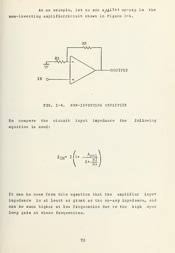
As an example, let us use a/XA741 op-amp in the
non-inverting amplif iercircuit shown in Figure 1-4.
IN o
O OUTPUT
FIG. 1-4. N0N-INVERTIN3 AMPLIFIER
To compute the circuit input impedance the following
eguation is used:
Z IN= Z/1+ Vol
1+—R2Rl
It can be seen from this equation that the amplifier input
impedance is at least as great as the op-amp irapsdance, and
can be raucn higher at lov frequencies due to the high open
loop gain at these frequencies.
73


106
105
104
103
102
10
1
10~ 1
X - Vc
741
= x1E= 25 c
V
\i C
I N I
!
I
ix
IX" II- \ i
i
\Ji \
10M 100
10 100 IK 10K TOOK 1M 10M
FREQUENCY - Hz
10 k
100 1 k 10k 100 :
FREQUENCY — Hz
1 M
1-5 1-6
Using this equation and tha data given in Figures 1-5 and
1-6, the dc input inpedance of the non-inverting amplifiercircuit with R2=9K ohms and R1=1 K ohms is 20,002 M ohms.
The same circuit operated at 100 KHZ would have an open loopgain of 10 and the input resistance of the op-amp would dropto 1.8 M ohms. With an input capacitance given by Figure1-6 of 2 pF, the op-amp input impedance would be given by
Z = 1.8M.TL// 2-rr (100kHz) 2x10
12- = 0. 5 5M .re-
using this value for Z in our original equation would give a
circuit input impedance of
Zin = 0.55 + 10(0.55)1 + 9
= l.lMru!
74

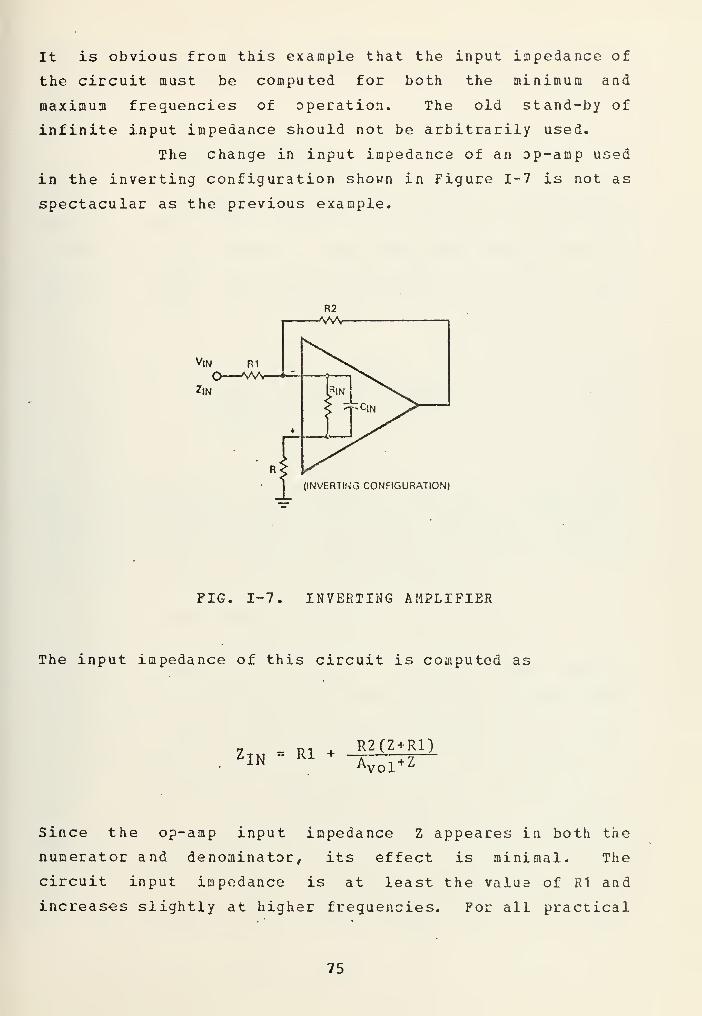
It is obvious from this example that the input impedance of
the circuit must be computed for both the minimum and
maximum frequencies of operation. The old stand-by of
infinite input impedance should not be arbitrarily used.
The change in input impedance of an Dp-amp used
in the inverting configuration shown in Figure 1-7 is not as
spectacular as the previous example.
(INVERTING CONFIGURATION)
FIG. 1-7 INVERTING AMPLIFIER
The input impedance of this circuit is computed as
IN= Rl +
R2(Z+R1)
Avol +Z
Since the op-amp input impedance Z appeares in both the
numerator and denominator, its effect is minimal. The
circuit input impedance is at least the valua of R1 and
increases slightly at higher frequencies. For all practical
75


applications in circuit design, it is safe to assume that
the input impedance of a inverting configuration amplifier
is just R.1.
d. Output Impedance
The output impedance is defined as tha impedance
seen by a load at the output of the device. The value
listed in data sheets is the open loop impedance and is
usually less than 200 ohns. For the/^A741 a value of 75
ohms is listed. The closed loop output impedance is given
by
Zoutclosedloop
outl +AVol x
TTTR1 + R2
and will increase as frequency increases. Since most
circuits utilizing op-amps are voltage amplifiers as opposed
to large current devices, the effect of output impedance
variations or load mismatch will be minimal.
e. Input Offset Voltage
Input offset voltage is defined as the voltage
that must be applied to the input terminals to obtain zero
output voltage, and typically is on the order of a few
millivolts. This is a very important op-amp parameter since
the input signal must overcome the offset voltage before an
output is produced. Additionally, with a common input at
both terminals an unwanted output voltage will be produced.
The amplifier gain increases the effect of offset voltage by
an amount equal to the gain plus one. For example, if the
ratio of R2 to 31 is 100, and the input offset voltage is 2
jnY (value for>u_A7U1), tha output voltage with zero input
76

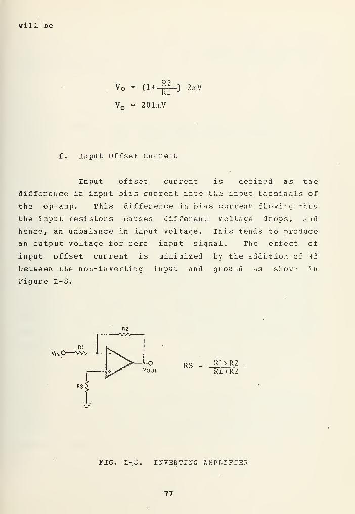
will be
V = (1+
V
R2Rl
= 201raV
-) 2mV
f. Input Offset Current
Input offset current is defined as the
difference in input bias current into the input terminals of
the op-amp. This difference in bias current flowing thru
the input resistors causes different voltage drops, and
hence, an unbalance in input voltage. This tends to produce
an output voltage for zero input signal. The effect of
input offset current is minimized by the addition of R3
between the non-inverting input and ground as shown in
Figure 1-8.
V|N —\w—i
n* _ RlxR2R3" ~RUR2
FIG. 1-8. INVERTING AMPLIFIER
77


The value of R3 is selected to equal the parallel
combination of R1 and R2. The output voltaga with zero
input signal is now
VQ = R2xI os where I os = input offset current
g. Common Mode Rejection Ratio
Common mode rejection ratio is defined as the
ratio of differential gain to common mode gain. It is an
indication of the degree of circuit balance in the
differential stages of the op-amp. If the stages were
perfectly balanced, a common mode signal applied to the
input terminals would be identically amplified on each side
and produce zero output. As a rule of thumb, CMRR should be
at least 20 db greater than the open loop gain and usually
much higher. The//A741 has a CMRR of 90 db. The CMRR
decreases with an increase in frequency because the open
loop gain, the numerator of the ratio, also decreases with
increasing frequency.
h. Stability
Although not an entry as such on a data sheet,
stability of an op-amp circuit must be understood to prevent
unwanted oscillations. The transfer functions for the
inverting and non- inverting configurations are given by the
following equations
78

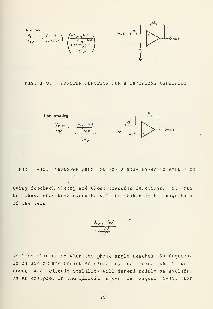
Inverting:
VOUT .
V.N \Z2 + 21 /
r-AVO!.AVOL ,u;
1 +
1 'Z2
z7
O vOUT
FIG. 1-9. TRANSFER FUNCTION FOR A INVERTING AMPLIFIER
Non-Inverting:
vOUT _
IN
AVQLMAV0LM
1 +
1 +Z2
zT
OVqut
FIG. 1-10. TRANSFER FUNCTION FOR A NON-INVERTING AMPLIFIER
Using feedback theory and these transfer functions, it can
be shown that both circuits will be stable if tli3 magnitude
of the term
Avol(^)
1*-Z2Zl
is less than unity when its phase angle reaches 180 degrees.
If Z1 and Z2 are resistive elements, no phase shift will
occur and circuit stability will depend mainly on Avol(f).
As an example, in the circuit shown in Figure 1-10, for
79


R2=10K ohms and R1 = 1 K ohms
1 + 11Zl
= 11 at 0° phase
When Avol(6J) = 11 the term
lvol C&0
1+-Z2Zl
= 1
From the open loop voltage gain curve of a/^ATUI given in
Figure 1-11 we see that Avol (6J) = 11 at a frequency of
aproximately 70 KHZ.
OPEN LOOP VOLTAGE GAINASA FUNCTION OF
FREQUENCY
UV
>
10
1
-"vlV
-V n c>
\ I
1
\ 1
j
N^
\
OPEN LOOP PHASE RESPONSEASA \ UNCTION OF
FREQUENCY
s -so
|
\ 1
' Vi«'
\
—V >-, ——— ,'
B 100 U kX tXk 1M KM
IKQVlNCY-hj
U id U » ut» in trt
I- II I-U
oo


From Figure 1-12 at a frequency of 70 KHZ we note a phase
shift of only 90 degrees, hence the circuit will be stable.
If the phase shift is more than 180 degrees with a unity
gain we have three alternatives in correcting the
instability. The easiest way would be to reduce the closed
loop gain to a point *here the stability criterion is
satisfied. Since this will not always meet our design
objectives we could select another op-amp with better high
frequency response. If this is not feasible, we could use a
compensating capacitor on the op-amp to change its open loop
gain vs. frequency response.
As an example, a JJo^lTl op-amp is used in the
inverting configuration of Figure 1-9 with Z2 and Z1 equal
and resistive. As before
1 + -11 = 2 at 0° phaseU J-
When Avol (f ) =2 the term
AVolM1+-
Z2Zl
= 1
From the open loop voltage gain curve of Figure 1-13 we see
that with a compensation capacitor (Cc) value of 30pF,
Avol=2 at a frequency of 500 KHZ. With Cc=3pF we note a
frequency of 5 MHZ.
81


1?0
100
eo
60
40
y JO
-201U) Ik kH 1 00 k 1 M 101
f REOUENCY - Hi
-30
-60
-9C
w -120<x
150
-180 -
-210
»l 2ki: i 1jA77 7
v' Co - 3 p* vs = • l b V— TA = '2bC' r-s • 501!
% i\A !
\Vt I
.1 .._•
I 10 K J 1» 1 » I UU » IM HIM
fREOUENCY - Hi
I- 13 I-H
To determine the more stable circuit, we note in Figure 1-14
that at a frequency of 5 MHZ we have a phase close to 130
degrees and the circuit is potentially unstable. The phase
shift at 500 KHZ is close to 110 degrees, therefore, the
compensation, Cc=30pF, should be used.
It should be noted that larger compensating
capacitors are not the answer to all stability problems. A
limit is reached where an increase in the size of the
compensating capacitor reduces the slew rate of the circuit
to the point of limiting the frequency response and
producing a distorted output.
a. Inverting Amplifiers
With a better insight into op-amp parameters we
are now ready to apply the knowledge gained to the design of
inverting amplifiers as shown in Figure 1-15.
82


Rl
V|N O W
FIG. 1-15 INVERTING AMPLIFIER
As with any design problem, a set of specifications will be
given , or they can be formulated from circuit requirements.
For this example, the following specifications are assumed:
Gain=9
Minimum 3 db down frequency 10 KHZ
Input resistance 10 K ohms
Maximum input signal amplitude 2 Vpk-pfc
Maximum dc output offset voltage ±65mV
DC drift from 0° to 70° C < 15 mV
For a gain of 9, the ratio of R2/R1 must equal
9. The first step is to determine the open loop gain
necessary to meet the closed loop gain at the specified
frequency. Using the equation that follows, an op-arap is
required that has an open loop gain of at least 28 db at 10
KHZ.
83


a T- 100 d+Y) Y+1 ^_100ili£i__ 8 ^28db
Avol * ^— ' ' 29.3
The next step is to compute the minimum slew
rate required for the expected output voltage swing. Since
the maximum input voltage specified is 2 Vpk-pk, the output
will be 9 times greater or 18 Vpk-pk.
SLEW RATE > 2TT f^x Vpk x 10~ 6 >0.S9 V/us
The third step is to compute input offset
voltage (Vos) and input offset current (Ios) that will meet
the maximum dc output offset (Vo) requirement of ± 65 mV.
The dc output offset voltage for the circuit in Figure 1
with R3=R1 in parallel with R2 is given by the following
equation:
Vo - (1+ ^ )V0S + R2xI 0S
From this equation it can be seen that Vo will be low if R2
is small; therefore the smallest possible value is chosen.
It was shown previously tiiat for the inverting configuration
the input resistance Rin is at least as great as F1. Our
specifications call for Rin=10K ohms; therefore, R1 is
selected so that
I*1 ^ Rin ^ 10K ohms
8U


If we choose R1=10K, R2 must equal 90 K ohms to achieve the
reguired gain of 9. R3 will then equal R1 in parallel with
R2 or 9 K ohms. With all the resistor values known we have
Vo = (1 + 9)V0S + (90xio 3)l ,
and for a maximum Yo of ±65 mV an op-amp is needed such that
Vos and Ios give
10VOS + (90xlCr)I os ^ 65mV ^ V (MAX)
The search for an op-aaip is greatly simplified by looking
for the following specifications:
Vq(MAX) 65V OS "£z — ^
10 106.5mV
Ios ^V (MAX)
90xl0 3270 nA
The last requirement is dc drift caused by a
temperature change over the range of 0° to 70° C. Drift is
given by
AV = IOaVqs + (100x10 3 )aI os ^ AVo(MAX)
85


where AVos and Alos are changes in input offset voltage and
current over the temperature range specified. These values
are found on a data sheet in the form of graphs.
To select the proper op-amp start with the first
and second requirements listed in the summary below. This
will eliminate many op-amps and the ones selected can then
be checked against the remaining requirements.
Avol>28db at 10 KHZ
slew rate>0.5V/,s
Vos<6. 5mV
Ios<270nA
Vo<15mV
The Fairchild/-CA7U 1 op-amp meets all the above reguiremints.
There are usually other specifications such as supply-
voltage and current, common mode rejection ratio, etc., that
should be considered. However, only a few op-amps will meet
these five requirements and further selection can be easily
made after the number of op-amps are narrowed down to a few.
b. Non-inverting Amplifiers
The design procedure for non-inverting
amplifiers, shown in Figure 1-16, is similar to that of
inverting amplifiers.
86


vOUT
FIG. 1-16. NON-INVERTING AMPLIFIER
For this example the following specifications are assumed:
Gain=10
Minimum 3 db down frequency 10 KHZ
Input resistance 5 M ohms
Maximum input signal amplitude 2 Vpk-pk
Maximum dc output offset voltage ±65 mV
DC drift from 0° to 70° C < 15 mV
For a gain of 10 the ratio of (R2+R1)/R1 must
equal 10..The first step, as before, is to determine the
open loop gain necessary to meet the closed loop gain at the
specified frequency. Using the equation below an op-amp is
required that has an open loop gain of at least 29 db at 10
KHZ.
Ayol100(1+Y) Y + l
100(1+10)W7Z 29db
The next step is to compute the minimum slew
rate required for the expected output voltage swing of 20
Vpk-pk."
87


SLEW RATE > 2lTfiMAX Vpkxl0"6 > 0.63 VU s
The third step is to compute the input impedance
for the non-inverting configuration given by
Avolz in = ZC1+ IOZ
Rl
where Z is the op-amp input impedance. The design calls for
an op^amp input impedance of 5 M ohms up to at least 10 KHZ.
He have already determined that Avol must be 29 db (or 28
V/V) at 10 KHZ. By substitution in the above equation the
required op-amp must have an input impedance at 10 KHZ of at
least the following:
= 1.3 M-n.Z IN 5M-n-
Avol1
R21+ Rl
1+ 2810
Figure 1-17 shows the curves for input resistance and
capacitance of 3.UK111 op-amp.
88

10M
1 M
a.
2
100 k
10k
4ffn
_ .1...
H
wiilLLLULDi{J_LIUL
1 {I
JK *
4-H 1—r-OT=t1±t_t_tt
-I
li ! i h i -4
=HH._ts= t&!
>
'
M+hi 1
1
1TQ-TTT-rl
illr
100
10
>_2
u<<
1u
Q-
2
100 1 k 10k 100k 1 MFREQUENCY— Hz
1
FIG. 1-17. INPUT RESISTANCE VS FREQUENCY
Input impedance is easily computed as the parallel
combination of these values at 10 KHZ. The value of 1.6 H
ohms indicates this op-amp would meet our input impedance
requirements.
Next we compute the dc output offset voltage for
the circuit in Figure 1-16 with R3=R1 in parallel with R2.
Vo - d+ -|j)Vos + R2 x I 0s
From this equation it can be seen that Vo will be low if R2
is small; therefore the smallest possible value is chosen.
R1 + R2Rl
= 10
If we choose R1=10 K ohms; then R2=90 K ohms and R3=9 K ohms
and we have
89


V = (l + 9)V s + (100 xlO-^Ios
For a maximum Vo of ± 65 mV an op-amp is needed such that
Vos and Ios give
lOVos +( 10 ° xl0 3 )I Os^ 65mV
The search for an op-amp is greatly simplified by looking
for the following specifications:
Vqs <"T0" <• 6 - 5mV
Ios < 650S <
100 xl0 3<650 nA
The last requirement is dc drift caused by a
temperature change over the range of 0° to 70° C. Drift, as
before, is given by
AV ^ 11aV0S + (100 xl0 3)M os ^aVo(MAX) 15 mV'
where A Vos andAIos are changes in input offset voltage and
current over the temperature range specified. These values
are found on a data sheet in the form of graphs.
The selection of the proper op-amp is done as
90


before, starting with the requirements for Avol first then
slew rate, input offset voltage, input offset current, etc.
4- Design Summary
a. Inverting Amplifiers
1. Determine the open loop gain necessary to
meet the closed loop gain at the specified frequency.
100JJJQ--Mnvol-^ X
2. Compute the minimum slew rate required for
the expected output voltage swing.
SLEW RATE> 2TT fm Vpk x 10" 6
3. Compute input offset voltage (Vos) and input
offset current (Ios) that will meet the maximum dc output
offset (Vo) requirement.
Vo = (1+ ^- )V0S + R2xI 0SRl
4. Select several op-amps that meet the
91


requirements of the first three steps and then narrow do*n
the choice by discarding those that do not meet the dc drift
specification.
b. Non-Inverting Amplifiers
1. Determine the open loop gain nacessary to
meet the closed loop gain at the specified frequency.
Avol> X100 (1+Y) _ y+1
2. Compute the minimum slew rate required for
the expected output voltage swing.
SLEW RATE > 27T fMAX V , x 10' 6
3. Compute the input impedance
Z IN = Z/1+
4. Compute input offset voltage (Vos) and input
offset current (Ios) that will meet the maximum -dc output
offset (Vo) requirement.
92


(1+ RT )Vos + R2xIos
5. Select several op-amps that meet the
requirements of the first four steps and then narrow down
the choice by discarding those that do not meet the dc drift
specification.
93

II. ADDITIONS TO THE ANALOG/DIGITAL IC TRAINER
The Breadboard on tha Analog/Digital IC Trainar provides
the capability for interconnecting 35 IC's. It was found
however, that the 1.75 ampere rating of the +5 volt power
supply limited the number of IC's that could be connected
before overloading. The following section describes an
entirely new power supply system that was designed and
implemented to overcome this limitation. Additionaly, a
section is included describing the Binary Display/Logic
Probe Module.
94


A. MAIN FRAME
1 • XHt£2^ii2i.1211
The Main Frame is the "heart" of the Analog/Digital
IC Trainer. It contains three built-in power supplies that
provide power to plug-in modules through circuit board edge
connectors. The Main Frame can accommodate up to five
modules and a breadboard. The breadboard is used to allow
the rapid interconnection of as many as thirty-five
integrated circuits. Two different Main Frames are
availiable, the difference being the output rating of the
power supplies. These different ratings are given in the
specifications below. The higher power Main Frames are
clearly marked "5 amperes" on the front panel for easy
identification.
2- Operation
Select the Main Frame best suited for the power
required. Most experiments that are included as part of the
Analog/Digital IC Trainer lesson package can be accomplished
on the lower rated Main Frame. If more than one Display
Module is to be used, or a large number of IC's are to be
interconnected, the Main Frame marked "5 amperes" should be
used. If in doubt, use the higher rated Main Frame.
To operate the Main Frame, turn the power switch,
located on the back panel, to the "off" position and plug
the cord into a standard 110 volt outlet. Insert modules as
needed and interconnect them to the breadboard. Standard
"banana" jacks are located on the front of the Main Frame to
provide + 5, +15, and -15 volts for interconnecting to the
breadboard as required. Make all connections to the modules
and breadboard with the power turned off. After connections
are made, turn the power on.
95


3 • Specifications
Low Power Main Frame
Input Power Voltage 110V AC
Power 50 Watts MAX
Output Power Voltage + 5V DC at 2 A
+ 15V DC at 500 mA
-15V DC at 500 raA
High power Main Frame
Input Power Voltage 110V AC
Power 100 Watts MAX
Output Power Voltage +5V DC at 5 A
+15V DC at 500 mA
-15V DC at 500 mA
f*« Circuit Description
The schematic diagram of the lower rated power
supply is shown on the following page. With S1 closed, line
voltage is applied to the primary of transformers T1 and 12
through fuse F1. The 15 volt secondary voltage of
transformer T1 is rectified by full wave bridge rectifiers
CR1 and CR2, and filtered by capacitors C1 and C2. IC
voltage regulators J1 and U2 [Ref. 6] regulate the voltage
at +15 and -15 volts which is then applied to the five edge
connectors and two banana jacks on the Main Frame.
The 12 volt secondary voltage of transformer T2 is
rectified by the full wave bridge rectifier CR3 and filtered
by capacitor C3. IC voltage regulator U3 [Ref. 6] regulates
the output voltage to +5 volts through the external pass
transistor Q1. The purpose of Q 1 is to increase the
regulated output current to 2 amperes. Resistor R1 provides
bias current for Q1.
96

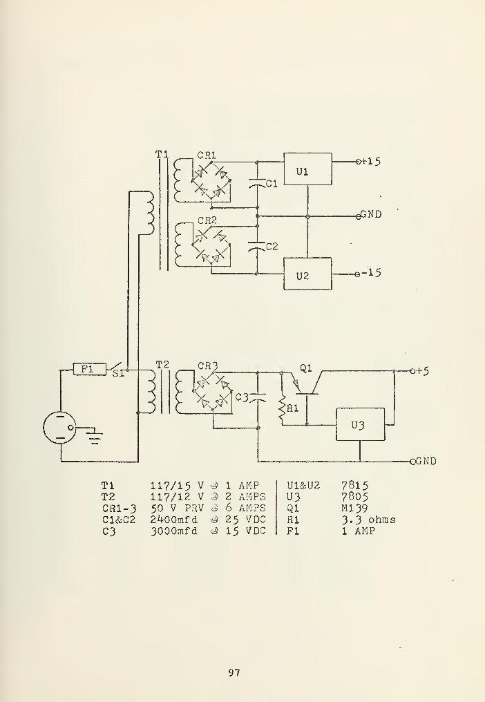
Tl CR1
CR3
Y
Ql
•Rl
€H-15
*£ND
-15
U3
ho+5
-OGND
Tl 117/15 V @ 1 AMP U1&U2 7815T2 117/12 V @ 2 AMPS U3 7805CR1-3 50 V PRV <3 6 AMPS Ql M139C1&C2 2400mfd $ 25 VDC Rl 3.3 ohmsC3 3000mfd ^ 15 VDC Fl 1 AMP
97


The schematic diagram of the high rated power supply
is shown below.
-*—
o
Tl 117/25.2 V @ 2.5 AMPS U2 Fairchild 79MG
T2 117/7.5 v ^8.0 AMPS HI 10k ohmsCR1 50 V PHV ^6.0 AMPS R2 7,22k ohmsCR2 100 v pav @ 25 AMPS R3 12.6k ohmsC1&C2 2200mfd & 50 VDC R4 16 ohmsC3&G^4- 10 mfd 25 VDC R5 0.17 ohmsC5&C6 8500mfd R6 % hois
c? •33mfd s 50 VDC Ql S7003C8 • lmfd @ 50 VDC Q2 2N28'l6
U1&U3 Fa ire hi Id 78MG Fl 1.5 AMPS
98


Kith switch S1 closed, line voltage is applied to the
primary of transformers T1 and T2 through fuse F1. The 25
volt secondary voltage of transformer T1 is rectified by the
full wave bridge rectifier C31. The positive and negative
voltages, with respect to ground, are filtered by capacitors
C1 and C2 respectively. IC voltage regulators J 1 and U2
[Ref. 7] form a dual tracking regulator with ±500 mA
capability. Resistors R1, R2, and R3 set the output voltage
of the regulators at ±15 volts. The output capacitors C3
and C4 are used to improve the transient response of the
system.
Because space liaitations in the Main Frame
precluded the use of a large transformer to supply the +5
volts at 5 amperes needed, transformer T2 was selected and
connected in a voltage doubler configuration. CR2 rectifies
the 7.5 volt output of T2 which is then doubled and filtered
by capacitors C5 and C6. Resistor RU sets the portion of
load current to be regulated directly by the IC regulator U3
[Ref. 7]. The series-pass transistor Q1 is used to achieve
the 5 amp output current of this power supply. Resistor B5
is a short circuit sensing resistor that works in
conjunction with Q2 to protect Q1 against short circuit
damage. As current through R5 increases above 5 amperes, Q2
begins to conduct and reduces the base current in Q1, which,
in turn, reduces the output current, thus protecting Q1.
Resistor R6 sets the voltage output of U3 at 5 volts. The
output capacitor C8 is used to improve transient response
while, capacitor Cl reduces the effect of the connecting
line inductance on regulator performance.
99


B. BINARY DISPLAY/LOGIC PROBE MODULE
1 • Ifi£iroduct ion
The Binary Display/Logic Probe Module permits the
display of up to 16 binary TTL logic signals simultaneously.
Connections for this display are made through 16 individual
pin inputs or through one 16 pin logic clip. The Logic
Probe portion of the module will indicate the logic state of
a circuit connection touched with a single-wire probe.
Colored lights are used to indicate either "low", "high", or
"open" circuit conditions.
2 . Operation
The front of the Binary Display/Logic Probe Module
is shown below.
PIN'a-
HIGH OPEN LOW
O O OO) PR03E
"\
ICCLIP
oooooooo
ooooooooo> o o o c o o
-*®
-LED's
100

When plugged into an energized Main Frame, the module is
"on". All 16 LED's grouped in the two rows will be on along
with the yellow "open circuit" indicating LED. To use the
binary display portion of the module, connect any of the
individual pin inputs located on the front of the module to
the circuit to be monitored. A logic clip can be used for
the interconnection if it is plugged into the 16 pin socket
and the switch positioned toward the socket. The LSD
corresponding to the pin input will be on for a "high" input
and off for a "low" input.
The Logic Probe portion of the module will display
the logic level oz a point in a system touched by the probe.
The circuitry contains provisions to stretch an input pulse
as short as 30 nano seconds, to one of 174 milliseconds.
This allows pulses of short duration to be displayed by an
LED. To test this portion of the module, touch the probe to
the + 5 volt supply line. The yellow light will go our and
the red light will come on, indicating a "high" logic
condition. Grounding the probe will cause the green light
to come on with all other lights out. WARNING: do not
touch tne probe to voltages higher than +5 volts or damage
to the module circuitry will result.
3 • Specifications
Power reguirments
Voltage +5 VDC ±15 VDC
Current 430 mA MAX
Logic +5 V TTL
101

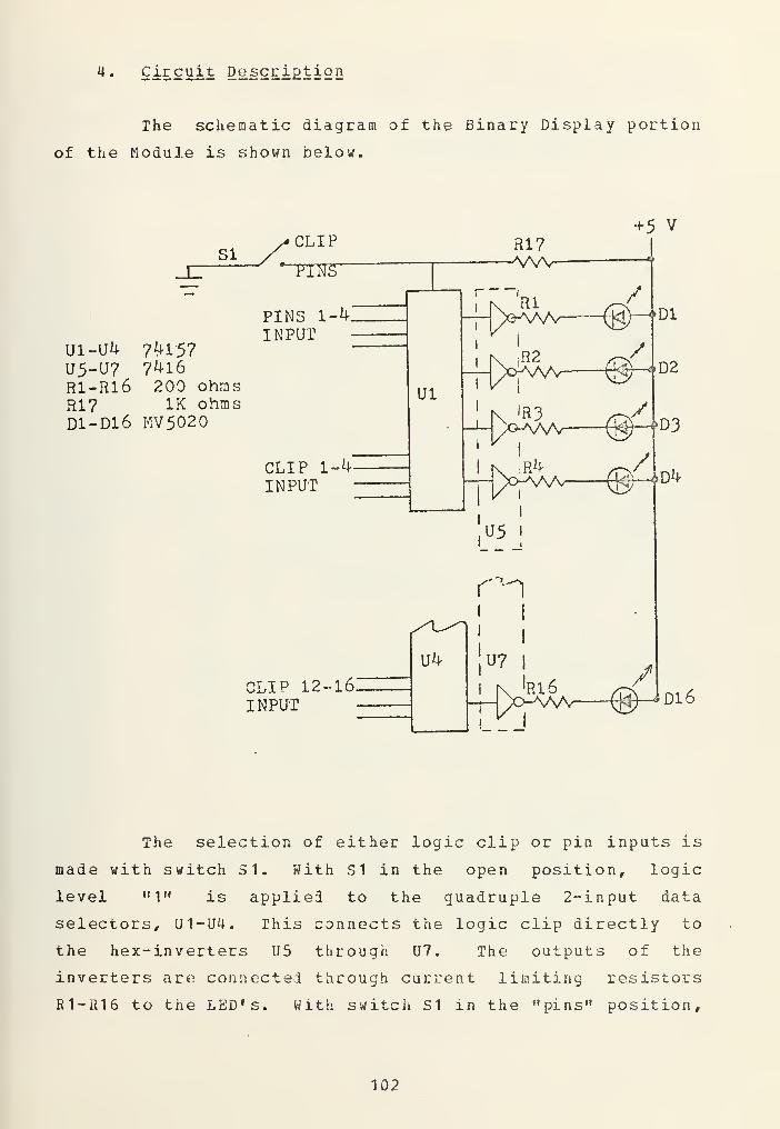
* Circuit Description
The schematic diagram of the Binary Display portion
of the Module is shown below.
SI
U1-U4 7^157U5-U7 7^16R1-R16 200 ohmsR17 IK ohmsD1-D16 MV5020
CLIP
' PINS
1-^:
INPUT
CLIP 1-J+-
INPUT
CLIP 12-161INPUT
Ul
U^
R17-WV
-fVwv @—<'
—N>Vw @H'
I 1
R3
R^-
U5 1
m• 1
!'
1 k 'ri6
T- /)cPvW
+5 v
J/
/
y
/
Dl
D2
-—N>AAA (J^r-^
D3
^-iDl6
The selection of either logic clip or pin inputs is
made with switch 31. With S1 in the open position, logic
level "1" is applied to the quadruple 2-input data
selectors, U1-U4. This connects the logic clip directly to
the hex-inverters U5 througn U7. The outputs of the
inverters are connected through current limiting resistors
R1-B16 to the LED's. With switch S1 in the "pins" position.
102


logic level "0" is applied to the data selectors, switching
them to the pin inputs. Resistor R17 is used for current
limiting.
The schematic diagram of the Logic Probe portion of
the Module is shown below.
PROBE'I^H^uT)^
"LOW"GREEN
Ul 7*HC02,7,8,9.11 7^161)3,5,6,10 7^00U4 7^123Dl-3 MV5020C1-C2 22rafd
Rl 510k ohmsR2 10MR3,6 1MR^,5 27kR7.8 10kR9-11 200812,13 24k
Resistors R1 through R6 form a voltage divider and
103


impeadance matching network which sets the non-inverting
input to U1 at 14.27 volts, and the inverting input at 7.5
volts with an "open" condition at the probe. In this
condition, the output of (J 1 is approximately +7 volts. This
+7 volts is reduced to + 3.5 volts by the voltage divider 37
and R8, and is then applied through inverter U2 to the
"open" indicator. Resistors R9-R11 are current limiters.
If the probe is touched to any voltage between and +5
volts, the non-inverting input of U1 will fall below the
inverting input, which will cause the output of U1 to go
negative. In this condition, the "open" indicator will go
out.
With the probe grounded or at logic level "0", the
output of U3 will be High and the output of the lower half
of U4 will be Low. The pulse stretching that is necessary
for the display of short pulses is accomplished by U4 . The
output of U9 will be Low, causing the output of J10 to oe
High and U 1 1 to be Low. This will light the green "low"
indicator.
With the probe at logic level "1", the output of LI
3
and the upper half of U4 will be Low. This action causes
the output of U5 to go High and U6 to go Low. U7 and U3 act
as a non-inverting buffer , so the low condition at the
output of U6 causes the "high" indicator to light. If the
input to the logic probe is a pulsed signal rather than a
level input, components C1, C2 and R12, R13 set the duration
of the output pulse, regardless of the duration of the input
pulse.
104

BIBLIOGRAPHY
1.
2.
3.
4.
Moellmer, K. A., Development of an Analogs/DigitalIntegrated Circuit Trainer, M.3.E.E. Tfies'is , 17 avalPostgraduate ScITool, Monterey, 1974.
Lancaster, Don, TTL Cookbook, Howard W. Sams, 1974.
TTL Data Book, Fairchild Semiconductor, June 1972.
Digital, Linear, MOS Data Book, Signetics Corporation,T9757— " r
5. Hamaoui«, Ii., "Op-Amps," Fairchild Journal ofSeniconciuctor Progress, v. 2, nos. d-TU, Hay-DecemberT9-74":
•
6. The Voltage Regulator Applications HandjK>o_iS/ FairchildSemi conductor, ~ 3arcK 19/4.
7. Pascoe, B., "Four Terminal Variable Voltage Regulators,"Fairchild Journal of Semiconductor Progress, v. 3, no.7, p. 3-
"9, January, February T975. "*
105


INITIAL DISTRIBUTION LIST
Defense Documentation Center
Cameron Station
Alexandria, Virgina 22314
No. Copies
1
2. Library, Code 0212
Naval Postgraduate School
Monterey, California. 93940
2. Department Chairman, Code 52
Department of Electrical Engineering
Naval Postgraduate School
Monterey, California 93940
4. Professor E. Panholzer, Code 52pz
Department of Electrical Engineering
Naval Postgraduate School
Monterey, California 93940
5. LCDR Daniel L. Wojtkowiak, USN
SMC 1454
Naval Postgraduate School
Monterey, California 93940
6. CDR Karl A. Moellmer, USN
Puget Sound Naval Shipyard
Bremerton, Washington 98314
106


»"!*« KNOX LIBRARY
Thesis >oOJLcW687 Wojtkowiakc.l Fundamentals and ap-
plications of integr-
ated ci rcui ts.

thesW687
Fundamentals and applications of integra
I II II II II
3 2768 000 98855 4DUDLEY KNOX LIBRARY