FULL PAPER Embossed Hollow …home.skku.edu/~nesel/paper files/120.pdf · 2014-05-07 · Our...
6
www.afm-journal.de FULL PAPER © 2013 WILEY-VCH Verlag GmbH & Co. KGaA, Weinheim 2038 www.MaterialsViews.com wileyonlinelibrary.com 1. Introduction Energy harvesting technologies may meet critical demand in areas where alternatives to fossil fuels are required for envi- ronmental protection, and in portable applications that require super-high energy capacity or complementary energy sources. Harvesting energy from ambient energy sources including solar, [1–8] thermal, [9] and mechanical energy, [10–18] has attracted intensive interest in the past years to meet these needs. Among these, piezoelectric harvesting technology, [12,14,19,20] which con- verts mechanical energy, the most common energy source available anywhere at any time, into electrical energy, has been proposed and investigated by many researchers because of an extended life time, no recharging proce- dures, and scalability. To date, there have been attempts to fabricate piezoelectric energy harvesting devices, named as nanogenerators, by employing various piezoelectric nanostructures including nanowires, [14,21–24] nanotubes, [25] and porous structures, [26] in which most works have been focused on nanowire-type gen- erators. However, these technologies still suffer from many drawbacks that limit the successful commercialization. Recently, thin film-type nanogenerators with per- ovskite ceramic materials (BaTiO 3 and ZnSnO 3 ) [27,28] were also demonstrated, generating a much higher level of power density than other similar structural or related devices. The advent of nanogenerator and nanotechnology may significantly lead to a self-powered system, based on driving portable devices with low power consump- tion by harvesting energy from ambient energy sources. Recent development in sensor technologies has provided innovative ways to reduce power consumption up to less than 1 mW, [29,30] enough to be produced by nanogenera- tors. Nanogenerator-assisted self-powered magnetic, [31] chem- ical, [32] temperature, [33] and mechanical sensors [34] have been successfully demonstrated. This approach can greatly enhance the adaptability, mobility, and durability of such sensors. Here, we introduce highly-ordered embossed thin films with hollow hemispheres as one of promising structures for nanogenera- tors and pressure sensors, produced by a spin coating of two- dimensional polystyrene spheres on planar substrates, followed by the deposition of ZnO layer by a radio-frequency magnetron sputtering method at room temperature and post-annealing. Embossed Hollow Hemisphere-Based Piezoelectric Nanogenerator and Highly Responsive Pressure Sensor Jinsung Chun, Keun Young Lee, Chong-Yun Kang, Myung Wha Kim, Sang-Woo Kim,* and Jeong Min Baik* Harvesting energy using piezoelectric materials such as ZnO, at nanoscale due to geometrical effects, are highly desirable for powering portable elec- tronics, biomedical, and healthcare applications. Although one-dimensional nanostructures such as nanowires have been the most widely studied for these applications, there exist a limited number of piezomaterials that can be easily manufactured into nanowires, thus, developing effective and reliable means of preparing nanostructures from a wide variety of piezomaterials is essential for the advancement of self-powered devices. In this study, ZnO embossed hollow hemispheres thin film for highly responsive pressure sen- sors and nanogenerators are reported. The asymmetric hemispheres, formed by an oblique angle deposition, cause an unsymmetrical piezoelectric field direction by external force, resulting in the control of the current direction and level at about 7 mA cm −2 at normal force of 30 N. The nanogenerators repeatedly generate the voltage output of ≈ ≈ 0.2 V, irrespective of the degree of symmetry. It is also demonstrated that when one piece of hemisphere layer is stacked over another to form a layer-by-layer matched architecture, the output voltage in nanogenerators increases up to 2 times. DOI: 10.1002/adfm.201302962 J. Chun, Prof. J. M. Baik School of Mechanical and Advanced Materials Engineering KIST-UNIST-Ulsan Center for Convergent Materials Ulsan National Institute of Science and Technology (UNIST) Ulsan, 689-798, Republic of Korea E-mail: [email protected] K. Y. Lee, Prof. S.-W. Kim School of Advanced Materials Science and Engineering Sungkyunkwan University (SKKU) Suwon, 440-746, Republic of Korea E-mail: [email protected] Dr. C.-Y. Kang Electronic Materials Research Center, KIST, Hwarangno 14-gil 5, Seongbuk-gu, Seoul, 137-791, Republic of Korea KU-KIST Graduate School of Converging Science and Technology Korea University 145, Anam-ro, Seongbuk-gu, Seoul, 136-701, Korea., Republic of Korea Prof. M. W. Kim Department of Chemistry & Nano Science Ewha Womans University Seoul, 120-750, Republic of Korea Adv. Funct. Mater. 2014, 24, 2038–2043
Transcript of FULL PAPER Embossed Hollow …home.skku.edu/~nesel/paper files/120.pdf · 2014-05-07 · Our...
www.afm-journal.de
FULL
PAPER
© 2013 WILEY-VCH Verlag GmbH & Co. KGaA, Weinheim2038
www.MaterialsViews.com
wileyonlinelibrary.com
1 . Introduction
Energy harvesting technologies may meet critical demand in areas where alternatives to fossil fuels are required for envi-ronmental protection, and in portable applications that require super-high energy capacity or complementary energy sources. Harvesting energy from ambient energy sources including solar, [ 1–8 ] thermal, [ 9 ] and mechanical energy, [ 10–18 ] has attracted intensive interest in the past years to meet these needs. Among these, piezoelectric harvesting technology, [ 12,14,19,20 ] which con-verts mechanical energy, the most common energy source available anywhere at any time, into electrical energy, has been proposed and investigated by many researchers because of an
extended life time, no recharging proce-dures, and scalability. To date, there have been attempts to fabricate piezoelectric energy harvesting devices, named as nanogenerators, by employing various piezoelectric nanostructures including nanowires, [ 14,21–24 ] nanotubes, [ 25 ] and porous structures, [ 26 ] in which most works have been focused on nanowire-type gen-erators. However, these technologies still suffer from many drawbacks that limit the successful commercialization. Recently, thin fi lm-type nanogenerators with per-ovskite ceramic materials (BaTiO 3 and ZnSnO 3 ) [ 27,28 ] were also demonstrated, generating a much higher level of power density than other similar structural or related devices.
The advent of nanogenerator and nanotechnology may signifi cantly lead to a self-powered system, based on driving portable devices with low power consump-tion by harvesting energy from ambient
energy sources. Recent development in sensor technologies has provided innovative ways to reduce power consumption up to less than 1 mW, [ 29,30 ] enough to be produced by nanogenera-tors. Nanogenerator-assisted self-powered magnetic, [ 31 ] chem-ical, [ 32 ] temperature, [ 33 ] and mechanical sensors [ 34 ] have been successfully demonstrated. This approach can greatly enhance the adaptability, mobility, and durability of such sensors. Here, we introduce highly-ordered embossed thin fi lms with hollow hemispheres as one of promising structures for nanogenera-tors and pressure sensors, produced by a spin coating of two-dimensional polystyrene spheres on planar substrates, followed by the deposition of ZnO layer by a radio-frequency magnetron sputtering method at room temperature and post-annealing.
Embossed Hollow Hemisphere-Based Piezoelectric Nanogenerator and Highly Responsive Pressure Sensor
Jinsung Chun , Keun Young Lee , Chong-Yun Kang , Myung Wha Kim , Sang-Woo Kim ,* and Jeong Min Baik *
Harvesting energy using piezoelectric materials such as ZnO, at nanoscale due to geometrical effects, are highly desirable for powering portable elec-tronics, biomedical, and healthcare applications. Although one-dimensional nanostructures such as nanowires have been the most widely studied for these applications, there exist a limited number of piezomaterials that can be easily manufactured into nanowires, thus, developing effective and reliable means of preparing nanostructures from a wide variety of piezomaterials is essential for the advancement of self-powered devices. In this study, ZnO embossed hollow hemispheres thin fi lm for highly responsive pressure sen-sors and nanogenerators are reported. The asymmetric hemispheres, formed by an oblique angle deposition, cause an unsymmetrical piezoelectric fi eld direction by external force, resulting in the control of the current direction and level at about 7 mA cm −2 at normal force of 30 N. The nanogenerators repeatedly generate the voltage output of ≈≈ 0.2 V, irrespective of the degree of symmetry. It is also demonstrated that when one piece of hemisphere layer is stacked over another to form a layer-by-layer matched architecture, the output voltage in nanogenerators increases up to 2 times.
DOI: 10.1002/adfm.201302962
J. Chun, Prof. J. M. Baik School of Mechanical and Advanced Materials Engineering KIST-UNIST-Ulsan Center for Convergent MaterialsUlsan National Institute of Science and Technology (UNIST) Ulsan , 689-798 , Republic of KoreaE-mail: [email protected] K. Y. Lee, Prof. S.-W. Kim School of Advanced Materials Science and Engineering Sungkyunkwan University (SKKU) Suwon , 440-746 , Republic of KoreaE-mail: [email protected]
Dr. C.-Y. Kang Electronic Materials Research Center, KIST, Hwarangno 14-gil 5, Seongbuk-gu, Seoul, 137-791, Republic of Korea KU-KIST Graduate School of Converging Science and Technology Korea University145, Anam-ro, Seongbuk-gu, Seoul, 136-701, Korea. , Republic of Korea Prof. M. W. Kim Department of Chemistry & Nano Science Ewha Womans University Seoul , 120-750 , Republic of Korea
Adv. Funct. Mater. 2014, 24, 2038–2043
FULL P
APER
2039
www.afm-journal.dewww.MaterialsViews.com
wileyonlinelibrary.com© 2013 WILEY-VCH Verlag GmbH & Co. KGaA, Weinheim
However, it is also demonstrated that the OAD does not enhance the performance of the nanogenerator.
2 . Results and Discussion
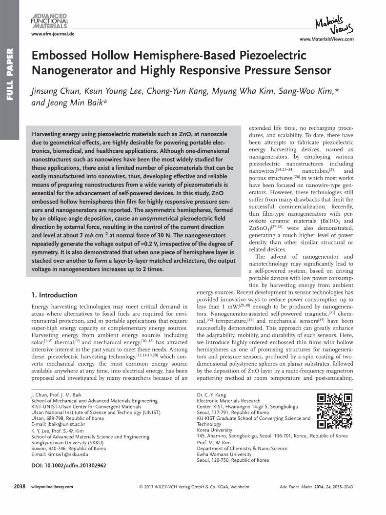
The schematic diagrams of the pressure sensor fabrication process are shown in Figure 1 a and detailed information described in Experimental section. Scanning electron microscopy (SEM) images in Figure 1 b shows that the 2D ZnO hollow hemisphere arrays are hexagonally close-packed as a form of multi-domains of areas larger than approximately 20 μ m 2 . By a spin coating method of PS spheres, quasi-continuous 2D array monolayers which fi ll the entire sub-strate of >10 cm 2 area are studied in the cur-rent study. By heating at 300 ° C for 1 h in
air, it produces ZnO embossed thin fi lms with hemispheres, well-distributed on the substrates.
The microstructure and crystalline properties of the embossed ZnO thin fi lms were characterized by transmis-sion electron microscopy (TEM) and X-ray diffraction (XRD). In the XRD spectrum ( Figure 2 a), there is only one peak cor-responding to the (0002) plane of ZnO, showing preferred orientation of ZnO thin fi lms. As the angle between sub-strate normal and vapor fl ux increases, the peak shifts to the higher angle by 0.3 ° and the full-width-half-maximum (FWHM) decreases from 0.32 ° to 0.3 ° , meaning an improve-ment in the crystallinity of the embossed fi lms deposited by OAD. Figure 2 b shows a cross-sectional TEM image of asym-metric hemispheres, which reveals that the hemispheres are hollow. Clearly, a fi lm was deposited directly on the substrate although the bottoms of the hemispheres fold into the hollow
inner space. The elemental maps, deter-mined by energy dispersive X-ray (EDX), of an embossed ZnO thin fi lm confi rms the formation of asymmetric hemispheres con-sisting of Zn and O atoms. The high-res-olution TEM (HR-TEM) images show that the fi lm clearly reveals columnar structures with grain sizes in the range of 10–20 nm. Each grain seems to be highly crystalline, based on the facts that the most part of the domains is bright in dark fi eld image, lattice fringes are well ordered. Furthermore, high magnifi cation at the domain interface clearly shows the crystalline continuity between the grains, indicating that the embossed ZnO fi lms enable reliable device action. It can also be seen that there are some stacking faults at the interface since the grains are fan-shaped (it means that the grain size increases from bottom to top).
Figure 3 a shows the change of the current density with the applied voltage of 10 mV when the external force of 30 N is applied. For
Our approach has the advantages of quasi-ordered 2D fi lms with large dimension (>280 cm 2 area), [ 35 ] precisely controlled multilayer structures via physical vapor deposition, and no lim-itation on materials. The embossed thin fi lm also has a high mechanical durability with good stretchable properties, com-pared with conventional thin fi lm.
Upon subsequent removal of the organic template by thermal decomposition, the ZnO fi lm exhibits a macro-porous structure with hollow hemispheres. For pressure sensors, later-ally aligned electrodes were formed by deposition of Ti/Au and indium wire bonding, while vertically arranged electrodes (ITO) on the top and bottom of the embossed hemispheres were used in the nanogenerator (detailed information is described in the experimental section). For enhancing the performance of the pressure sensors, we employed an oblique angle deposition (OAD) technique which makes the hemispheres asymmetric.
Figure 1. a) Schematic diagrams of the pressure sensor fabrication process. b) Hexagonally close-packed 2D arrays as a form of multi-domains of areas larger than approximately 20 μ m 2 . Oblique angle deposition of ZnO ( θ = 85 ° ) produced asymmetric hemispheres.
Figure 2. a) The XRD patterns of ZnO thin fi lms with symmetric and asymmetric hollow hemi-spheres on SiO 2 /Si substrate. b) A cross-sectional TEM image and EDX results of asymmetric shaped hemispheres, which reveals that the hemispheres are hollow and consist of Zn and O atoms. The HR-TEM images also show that the hemisphere has columnar structures with grain sizes in the range of 10–20 nm. High crystallinity of each grain, based on facts that the most part of the grains is bright in dark fi eld image and lattice fringes are well ordered.
Adv. Funct. Mater. 2014, 24, 2038–2043

FULL
PAPER
2040
www.afm-journal.dewww.MaterialsViews.com
wileyonlinelibrary.com © 2013 WILEY-VCH Verlag GmbH & Co. KGaA, Weinheim
thin fi lm and embossed thin fi lm with symmetric hemispheres, there is no change in the current density when we push the samples, as shown in the inset, although there is a little change (<0.05 mA cm −2 ) in the embossed fi lm by the force. By making the hemispheres asymmetric, a sharp current pulse up to 7 mA cm −2 was clearly observed when the sample was pushed quickly. The unsymmetrical pressure between the tensile and compressive stressed region in hemispheres along lateral direc-tion causes a gradient in the piezoelectric potential, resulting in the control of the current direction and level to be approxi-mately 7 mA cm −2 at the normal force of 30 N. If the sensitivity of the pressure sensor is defi ned to be S = ( I p – I o )/ I o p , where p denotes the applied pressure, I p and I o denote the current with and without applied pressure, the sensitivity of the sensor with asymmetric hemispheres is calculated to be 1.64 kPa −1 , higher than those of fi lm and symmetric hemispheres. The change of current density by a pushing force in embossed fi lms with hollow hemispheres can be understood from the piezoelectric potential distributions inside a hemisphere along the direction (Figure 3 b). A COMSOL package was used to investigate the piezoelectric potential distribution inside the hemisphere. In case of the thin fi lm, it is not likely to deform by such pushing force, evident by no change of current density. The asymmetric hemisphere causes an unsymmetrical strain distribution along the transverse direction due to the pushing force. Specifi cally, strain gradient is dominant and the stress is dominantly distrib-uted at the bottom area of the thicker hemisphere (see left side at near bottom of the hemisphere). The gradient of the piezoe-lectric potential near the bottom of the hemisphere resulted in a net electrical fi eld along the transverse direction. However, for a symmetric hemisphere, the electric fi eld direction and the piezo-electric potential by external force are seen to be same, resulting in a zero net electric fi eld and no change of current density.
When a measurement instrument is forward connected to the device, the device showed a positive current upon the pushing states ( Figure 4 ). In the case of the reverse connection, the negative current pulses are measured. This result indicates that the measured current are the true signals generated from the devices strained by pushing motions. Figure 5 also shows
Figure 3. a) The change of the current density with the applied voltage of 10 mV when the external force of 30 N is applied and b) piezoelectric poten-tial distributions inside a hemisphere along the direction (transverse and vertical) for symmetric (top) and asymmetric (bottom) hollow hemispheres.
Figure 4. The output current signals of the embossed thin fi lm measured in the forward connection and in the reverse connection.
Figure 5. The change of current density of the sensor with the magnitude of applied forces (5, 10, 20, and 30 N).
Adv. Funct. Mater. 2014, 24, 2038–2043
FULL P
APER
2041
www.afm-journal.dewww.MaterialsViews.com
wileyonlinelibrary.com© 2013 WILEY-VCH Verlag GmbH & Co. KGaA, Weinheim
the change of current density of the sensor with the magnitude of applied force. It can be clearly seen that the change of the cur-rent density increased nearly linearly as the external force increased from 0.5 to 30 N for the ZnO embossed fi lm.
On the contrary, it is seen that piezoelectric potential distributions are at the same level along the vertical direction, irrespective of the degree of symmetry. To verify it, we meas-ured the output voltage of the embossed fi lm-type nanogenerator, sandwiched between the top and bottom electrodes by pushing the fi lm. As shown in Figure 6 a, nanogen-erator with this design has a four-layer struc-ture. Figure 6 b shows SEM images of the
embossed ZnO thin fi lm nanogenerator with symmetric and asymmetric hemispheres. The performance of the nanogen-erator was then tested; the results are shown in Figure 7 a. By pushing the nanogenerator, the embossed fi lm with symmetric hemispheres repeatedly generates an open-circuit voltage of ≈ 0.2 V, which is the same voltage in embossed fi lm with asym-metric hemispheres. The simulation results along the vertical direction are clearly seen in Figure 7 b. A nanogenerator was also made by stacking two layers of such hemispheres layer-by-layer. It was done by spin-coating of the polystyrene on the hemispheres, followed by the deposition of ZnO fi lm and post annealing. The layer-by-layer integrated nanogenerator shows the enhanced output voltage of ≈ 0.4 V as the sum of the output voltage of ≈ 0.2 V from the two individual hemispheres, as shown in Figure 8 .
3 . Conclusions
In summary, we reported ZnO embossed hollow hemi-spheres thin fi lm for highly responsive pressure sensors and
Figure 6. a) The schematic diagrams of the nanogenerator fabrication process. b) Low and high magnifi cation SEM images of the nanogenerator.
Figure 7. a) Open-circuit voltage and b) piezoelectric potential distributions of nanogenerators with symmetric (top) and asymmetric (bottom) hollow hemispheres.
Figure 8. Open-circuit voltage of embossed thin fi lm generator with single-layered and two-layered hollow hemispheres.
Adv. Funct. Mater. 2014, 24, 2038–2043

FULL
PAPER
2042
www.afm-journal.dewww.MaterialsViews.com
wileyonlinelibrary.com © 2013 WILEY-VCH Verlag GmbH & Co. KGaA, Weinheim
Acknowledgements J.C. and K.Y.L. contributed equally to this work. This work was fi nancially supported by the National Research Foundation of Korea (NRF) grant funded by the Ministry of Education, Science and Technology (MEST) (2012R1A2A1A01002787), the IT R&D program of MKE/KEIT [10035598, 180 lm/W High-effi ciency nano-based LEDs], and by the Future Strategic Fund(1.130061.01) of UNIST(Ulsan National Institute of Science and Technology).
Received: August 24, 2013 Revised: October 3, 2013
Published online: November 19, 2013
[1] A. Hagfeldt , M. Gratzel , Acc. Chem. Res. 2000 , 33 , 269 – 277 . [2] M. K. Nazeeruddin , A. Kay , I. Rodicio , R. Humphrybaker , E. Muller ,
P. Liska , N. Vlachopoulos , M. Grätzel , J. Am. Chem. Soc. 1993 , 115 , 6382 – 6390 .
[3] B. Oregan , M. Gratzel , Nature 1991 , 353 , 737 – 740 . [4] W. U. Huynh , J. J. Dittmer , A. P. Alivisatos , Science 2002 , 295 ,
2425 – 2427 . [5] Q. B. Pei , G. Yu , C. Zhang , Y. Yang , A. J. Heeger , Science 1995 , 269 ,
1086 – 1088 . [6] G. Yu , J. Gao , J. C. Hummelen , F. Wudl , A. J. Heeger , Science 1995 ,
270 , 1789 – 1791 . [7] B. Z. Tian , X. L. Zheng , T. J. Kempa , Y. Fang , N. F. Yu , G. H. Yu ,
J. Huang , C. M. Lieber , Nature 2007 , 449 , 885 – 889 . [8] I. Gur , N. A. Fromer , M. L. Geier , A. P. Alivisatos , Science 2005 , 310 ,
462 – 465 . [9] Y. Yang , W. Guo , K. C. Pradel , G. Zhu , Y. Zhou , Y. Zhang , Y. Hu ,
L. Lin , Z. L. Wang , Nano Lett. 2012 , 12 , 2833 – 2838 . [10] Z. L. Wang , J. H. Song , Science 2006 , 312 , 242 – 246 . [11] Z. L. Wang , Sci. Am. 2008 , 298 , 82 – 87 . [12] X. D. Wang , J. H. Song , J. Liu , Z. L. Wang , Science 2007 , 316 ,
102 – 105 . [13] Y. Qin , X. D. Wang , Z. L. Wang , Nature 2008 , 451 , 809 – 813 . [14] R. S. Yang , Y. Qin , L. M. Dai , Z. L. Wang , Nat. Nanotechnol. 2009 , 4 ,
34 – 39 . [15] S. Xu , Y. Qin , C. Xu , Y. Wei , R. Yang , Z. L. Wang , Nat. Nanotechnol.
2010 , 5 , 366 – 373 . [16] D. Choi , M.-Y. Choi , W. M. Choi , H.-J. Shin , H. K. Park , J. S. Seo ,
J. Park , S. M. Yoon , S. J. Chae , Y. H. Lee , S.-W. Kim , J.-Y. Choi , S. Y. Lee , J. M. Kim , Adv. Mater. 2010 , 22 , 2187 – 2192 .
[17] K. Y. Lee , B. Kumar , J.-S. Seo , K.-H. Kim , J. I. Sohn , S. N. Cha , D. Choi , Z. L. Wang , S.-W. Kim , Nano Lett. 2012 , 12 , 1959 – 1964 .
[18] S. Lee , J.-I. Hong , C. Xu , M. Lee , D. Kim , L. Lin , W. Hwang , Z. L. Wang , Adv. Mater. 2012 , 24 , 4398 – 4402 .
[19] C. E. Chang , V. H. Tran , J. B. Wang , Y. K. Fuh , L. W. Lin , Nano Lett. 2010 , 10 , 726 – 731 .
[20] S. Xu , B. J. Hansen , Z. L. Wang , Nat. Commun. 2010 , 1 . [21] G. Zhu , A. C. Wang , Y. Liu , Y. Zhou , Z. L. Wang , Nano Lett. 2012 , 12 ,
3086 – 3090 . [22] S. Lee , S.-H. Bae , L. Lin , Y. Yang , C. Park , S.-W. Kim , S. N. Cha ,
H. Kim , Y. J. Park , Z. L. Wang , Adv. Funct. Mater. 2012 , 23 , 2445 – 2449 . [23] L. Lin , Y. Hu , C. Xu , Y. Zhang , R. Zhang , X. Wen , Z. L. Wang , Nano
Energy 2013 , 2 , 75 – 81 . [24] S. Lee , J.-I. Hong , C. Xu , M. Lee , D. Kim , L. Lin , W. Hwang ,
Z. L. Wang , Adv. Mater. 2012 , 24 , 4398 – 4402 . [25] Z.-H. Lin , Y. Yang , J. M. Wu , Y. Liu , F. Zhang , Z. L. Wang , J. Phys.
Chem. Lett. 2012 , 3 , 3599 – 3604 . [26] S. Cha , S. M. Kim , H. Kim , J. Ku , J. I. Sohn , Y. J. Park , B. G. Song ,
M. H. Jung , E. K. Lee , B. L. Choi , J. J. Park , Z. L. Wang , J. M. Kim , K. Kim , Nano Lett. 2011 , 11 , 5142 – 5147 .
piezoelectric nanogenerators. The asymmetric hemispheres, formed by an oblique angle deposition, caused an unsymmet-rical piezoelectric fi eld direction by external force, resulting in the control of the current direction and level at about 7 mA cm −2 at normal force of 30 N. The nanogenerators repeatedly gen-erate the voltage output of ≈ 0.2 V, irrespective of the degree of symmetry. We also demonstrated that when one piece of hemi-sphere layer is stacked over another to form a layer-by-layer matched architecture, the output voltage in nanogenerators increases up to 2 times. This technique will make high-output nanogenerator possible.
4 . Experimental Section Production of ZnO Thin Films with Hollow Hemisphres : An aqueous
suspension of 1- μ m-diameter polystyrene beads (2.6 wt%, Polysciences, Warrington, USA) was used to prepare close-packed monolayer bead templates for the fabrication of embossed ZnO fi lms, as described previously. Briefl y, prior to spin-coating of the suspension on bare SiO 2 /Si (for pressure sensors) and ITO-coated SiO 2 /Si (for nanogenerators) substrates, the bare substrate was treated with UV/Ozone (AHTECH LTS, South Korea), making the surface of the substrate hydrophilic. A drop of polystyrene bead suspension was then pipette onto the SiO 2 /Si substrate. Spin-coating of the polystyrene beads was done at 1300 rpm for 3 s, and then the sample was dried for 1 h in a dry box at room temperature. The spinning speed and slow drying were optimized because both were critical in obtaining monolayer bead templates without sphere-free regions or agglomeration. A 200-nm-thick ZnO fi lm was deposited onto the substrates at room temperature by a RF sputtering, and it can be optimized further for a better device performance. The base pressure, working pressure, rf power, and gas fl ow rate were 1 × 10 −6 Torr, 4 mTorr, 16/4 sccm (Ar/O 2 ), respectively. The hemispheres with asymmetric shapes were formed by OAD using a RF sputtering with a vapor fl ux angle of 85 ° . The samples were calcined in air at 300 ° C for 60 min to burn out the polymer beads and simultaneously crystallize the ZnO fi lm, resulting in an embossed ZnO fi lm with hollow hemispheres on the substrate.
Fabrication of Pressure Sensors and Electrical Properties Measurement : For pressure sensors, laterally arranged Ti/Au (20/200 nm) electrodes were then deposited using electron beam evaporation at a base pressure of 3.0 × 10 −6 Torr and bonded by Au wires (Figure 1 a,b). The external force was applied by pushing the insulating Tefl on block put on the embossed fi lms. Exact values of applied force, by using a force testing system of Mecmesin Multitest i-1 (Slinfold, United Kingdom) were measured by using an electronic scale. I–V characteristics with the applied force were measured under air ambient using a Keithley 2636A source measurement unit.
Fabrication of Nanogenerator and the Measurement of Output Voltage : For nanogenerators, a layer of 2 μ m thick poly(methyl methacrylate) (PMMA) was spin-coated on the embossed ZnO fi lms. As a top electrode, ITO layer was then placed above the heads of the embossed ZnO fi lms (Figure 6 a,b). A nanogenerator was also made by stacking two pieces of the hemispheres. We measured the output voltages of the embossed thin fi lm generators by applying a pushing force. To detect currents and voltages generated by Embossed thin fi lm nanogenerator, a Keithley 6485 picoammeter and Keithley 2182A nanovoltmeter ( R = 10 G Ω ) were used.
Microstructural Analysis : The morphologies of the synthesized ZnO fi lms were characterized by a Nano 230 fi eld emission scanning electron microscope (FEI, USA). Transmission electron microscopy was performed using a transmission electron microscope (JEOL, Japan). A dual-beam focus ion beam (FEI, USA) was used to prepare the TEM samples. The crystalline properties of the fi lms were characterized by a high resolution X-ray diffractometer (Bruker, Germany).
Adv. Funct. Mater. 2014, 24, 2038–2043

FULL P
APER
2043
www.afm-journal.dewww.MaterialsViews.com
wileyonlinelibrary.com© 2013 WILEY-VCH Verlag GmbH & Co. KGaA, Weinheim
[31] Y. Yang , L. Lin , Y. Zhang , Q. Jing , T.-C. Hou , Z. L. Wang , ACS Nano 2012 , 6 , 10378 – 10383 .
[32] P.-H. Yeh , Z. Li , Z. L. Wang , Adv. Mater. 2009 , 21 , 4975 – 4978 . [33] Y. Yang , Y. Zhou , J. M. Wu , Z. L. Wang , ACS Nano 2012 , 6 , 8456 – 8461 . [34] W. Wu , X. Wen , Z. L. Wang , Science 2013 , 340 , 952 – 957 . [35] J.-T. Zhang , L. Wang , D. N. Lamont , S. S. Velankar , S. A. Asher ,
Angew. Chem. Int. Ed. 2012 , 51 , 6117 – 6120 .
[27] K. I. Park , S. Xu , Y. Liu , G.-T. Hwang , S.-J. L. Kang , Z. L. Wang , K. J. Lee , Nano Lett. 2010 , 10 , 4939 – 4943 .
[28] J. M. Wu , C. Xu , Y. Zhang , Z. L. Wang , ACS Nano 2012 , 6 , 4335 – 4340 .
[29] E. Strelcov , S. Dmitriev , B. Button , J. Cothren , V. Sysoev , A. Kolmakov , Nanotechnology 2008 , 19 , 355502 .
[30] C.-H. Pan , H.-Y. Hsieh , K.-T. Tang , Sensors 2013 , 13 , 193 – 207 .
Adv. Funct. Mater. 2014, 24, 2038–2043