Full Frame 3D snapshot
167
Full frame 3D snapshot Possibilities and limitations of 3D image acquisition without scanning Examensarbete utfört i Datorteknik av Björn Möller LITH-ISY-EX--05/3734--SE Linköping 2005
Transcript of Full Frame 3D snapshot

Full frame 3D snapshotPossibilities and limitations of 3D
image acquisition without scanning
Examensarbete utfört i Datorteknikav
Björn Möller
LITH-ISY-EX--05/3734--SELinköping 2005


Full frame 3D snapshotPossibilities and limitations of 3D
image acquisition without scanning
Examensarbete utfört i Datorteknikvid Linköpings tekniska högskola
av
Björn MöllerLITH-ISY-EX--05/3734--SE
Handledare: Mattias Johannesson, Henrik Turbell
Examinator: Dake LiuLinköping 2005-04-05

Avdelning, Institution Division, Department
Institutionen för systemteknik 581 83 LINKÖPING
Datum Date 2005-03-24
Språk Language
Rapporttyp Report category
ISBN
Svenska/Swedish X Engelska/English
Licentiatavhandling X Examensarbete
ISRN LITH-ISY-EX--05/3734--SE
C-uppsats D-uppsats
Serietitel och serienummer Title of series, numbering
ISSN
Övrig rapport ____
URL för elektronisk version http://www.ep.liu.se/exjobb/isy/2005/3734/
Titel Title
Helbilds 3D-avbildning Full frame 3D snapshot - Possibilities and limitations of 3D image acquisition without scanning
Författare Author
Björn Möller
Sammanfattning Abstract An investigation was initiated, targeting snapshot 3D image sensors, with the objective to match the speed and resolution of a scanning sheet-of-light system, without using a scanning motion. The goal was a system capable of acquiring 25 snapshot images per second from a quadratic scene with a side from 50 mm to 1000 mm, sampled in 512×512 height measurement points, and with a depth resolution of 1 µm and beyond. A wide search of information about existing 3D measurement techniques resulted in a list of possible schemes, each presented with its advantages and disadvantages. No single scheme proved successful in meeting all the requirements. Pulse modulated time-of-flight is the only scheme capable of depth imaging by using only one exposure. However, a resolution of 1 µm corresponds to a pulse edge detection accuracy of 6.67 fs when visible light or other electromagnetic waves are used. Sequentially coded light projections require a logarithmic number of exposures. By projecting several patterns at the same time, using for instance light of different colours, the required number of exposures is reduced even further. The patterns are, however, not as well focused as a laser sheet-of-light can be. Using powerful architectural concepts such as matrix array picture processing (MAPP) and near-sensor image processing (NSIP) a sensor proposal was presented, designed to give as much support as possible to a large number of 3D imaging schemes. It allows for delayed decisions about details in the future implementation. It is necessary to relax at least one of the demands for this project in order to realise a working 3D imaging scheme using concurrent technology. One of the candidates for relaxation is the most obvious demand of snapshot behaviour. Furthermore, there are a number of decisions to make before designing an actual system using the recommendations presented in this thesis. The ongoing development of electronics, optics, and imaging schemes might be able to meet the 3D snapshot demands in a near future. The details of light sensing electronics must be carefully evaluated and the optical components such as lenses, projectors, and fibres should be studied in detail.
Nyckelord Keyword Snapshot 3D imaging, depth measurement, triangulation, interferometry, time-of-flight, CMOS image sensors


Abstract
An investigation was initiated, targeting snapshot 3D image sensors, with the objectiveto match the speed and resolution of a scanning sheet-of-light system, without using ascanning motion. The goal was a system capable of acquiring 25 snapshot images persecond from a quadratic scene with a side from 50 mm to 1000 mm,sampled in 512×512height measurement points, and with a depth resolution of 1µm and beyond.
A wide search of information about existing 3D measurement techniques resulted in alist of possible schemes, each presented with its advantages and disadvantages. No singlescheme proved successful in meeting all the requirements. Pulse modulated time-of-flight is the only scheme capable of depth imaging by using only one exposure. However,a resolution of 1µm corresponds to a pulse edge detection accuracy of 6.67 fs whenvisible light or other electromagnetic waves are used. Sequentially coded light projectionsrequire a logarithmic number of exposures. By projecting several patterns at the sametime, using for instance light of different colours, the required number of exposures isreduced even further. The patterns are, however, not as wellfocused as a laser sheet-of-light can be.
Using powerful architectural concepts such asmatrix array picture processing(MAPP)andnear-sensor image processing(NSIP) a sensor proposal was presented, designed togive as much support as possible to a large number of 3D imaging schemes. It allows fordelayed decisions about details in the future implementation.
It is necessary to relax at least one of the demands for this project in order to rea-lise a working 3D imaging scheme using concurrent technology. One of the candidatesfor relaxation is the most obvious demand of snapshot behaviour.Furthermore, there area number of decisions to make before designing an actual system using the recommen-dations presented in this thesis. The ongoing development of electronics, optics, andimaging schemes might be able to meet the 3D snapshot demandsin a near future. Thedetails of light sensing electronics must be carefully evaluated and the optical componentssuch as lenses, projectors, and fibres should be studied in detail.
vii


Acknowledgement
I would like to acknowledge the following people for helpingme forward on this bumpyroad.
• Thanks to professor Dake Liu who allocated time to examine this work.
• My supervisors at SICK IVP, dr Mattias Johannesson and dr Henrik Turbell areacknowledged for their valuable guidance through my first fumbling and waveringsteps in this vast jungle.
• SICK IVP and dr Mats Gökstorp made the project possible in thefirst place.
• Johan Melander, manager of the sensor design at SICK IVP, always supported meand protected the time given to me for this project.
• Thanks to my opponent Robert Johansson for his support on thetools front, for hisdeep knowledge in languages and CMOS sensors, and for being extremely patientwith me.
• Thanks to dr Annika Rantzer, Håkan Thorngren, Leif Lindgren, and everybody elseat SICK IVP for valuable input during discussions at the coffee table.
• Thanks to Frank Blöhbaum at SICK AG for valuable input on the PMD sensor andToF issues.
ix


Table of contents
Abstract vii
Acknowledgement ix
1 Definitions and abbreviations 1
1.1 Concept definitions . . . . . . . . . . . . . . . . . . . . . . . . . . . . . 1
1.2 Abbreviations . . . . . . . . . . . . . . . . . . . . . . . . . . . . . . . . 5
I Overview 7
2 Contents 92.1 Background . . . . . . . . . . . . . . . . . . . . . . . . . . . . . . . . . 9
2.2 Conditions for the project . . . . . . . . . . . . . . . . . . . . . . . . .. 10
2.3 Working methodology . . . . . . . . . . . . . . . . . . . . . . . . . . . 10
3 Goals for the project 13
3.1 Main project goal . . . . . . . . . . . . . . . . . . . . . . . . . . . . . . 13
3.2 Snapshot behaviour . . . . . . . . . . . . . . . . . . . . . . . . . . . . . 13
3.3 Speed . . . . . . . . . . . . . . . . . . . . . . . . . . . . . . . . . . . . 14
3.4 Z resolution . . . . . . . . . . . . . . . . . . . . . . . . . . . . . . . . . 14
3.5 X×Y resolution . . . . . . . . . . . . . . . . . . . . . . . . . . . . . . . 15
3.6 Communication requirements . . . . . . . . . . . . . . . . . . . . . . .. 16
3.7 Field of view . . . . . . . . . . . . . . . . . . . . . . . . . . . . . . . . 17
3.8 Production feasibility . . . . . . . . . . . . . . . . . . . . . . . . . . .. 17
3.9 Object surface dependence . . . . . . . . . . . . . . . . . . . . . . . . .18
3.10 Detection of surface properties . . . . . . . . . . . . . . . . . . .. . . . 19
xi

xii
II 3D imaging schemes 21
4 General 3D image acquisition 234.1 Triangulation schemes . . . . . . . . . . . . . . . . . . . . . . . . . . . 23
4.1.1 Focusing schemes . . . . . . . . . . . . . . . . . . . . . . . . . 244.1.2 Schemes using structured light . . . . . . . . . . . . . . . . . . .254.1.3 Passive schemes . . . . . . . . . . . . . . . . . . . . . . . . . . 26
4.2 Interferometric schemes . . . . . . . . . . . . . . . . . . . . . . . . . .. 274.2.1 Phase-shifting . . . . . . . . . . . . . . . . . . . . . . . . . . . . 28
4.3 Time-of-flight schemes . . . . . . . . . . . . . . . . . . . . . . . . . . . 29
5 3D image acquisition schemes 315.1 Beam-of-light triangulation . . . . . . . . . . . . . . . . . . . . . .. . . 315.2 Sheet-of-light triangulation . . . . . . . . . . . . . . . . . . . . .. . . . 325.3 Confocal microscopy . . . . . . . . . . . . . . . . . . . . . . . . . . . . 345.4 Self-adjusting focus . . . . . . . . . . . . . . . . . . . . . . . . . . . . .365.5 Depth from defocus . . . . . . . . . . . . . . . . . . . . . . . . . . . . . 375.6 Moiré . . . . . . . . . . . . . . . . . . . . . . . . . . . . . . . . . . . . 385.7 Sequentially coded light . . . . . . . . . . . . . . . . . . . . . . . . . .41
5.7.1 Colour coding . . . . . . . . . . . . . . . . . . . . . . . . . . . 435.8 Stereo vision . . . . . . . . . . . . . . . . . . . . . . . . . . . . . . . . 45
5.8.1 Several 2D cameras in known relative geometry . . . . . . .. . . 485.8.2 Several 2D cameras with dynamic self-adjustment . . . .. . . . 485.8.3 Single self-adjusting 2D camera taking several images . . . . . . 485.8.4 Motion parallax . . . . . . . . . . . . . . . . . . . . . . . . . . . 48
5.9 Shape from shading . . . . . . . . . . . . . . . . . . . . . . . . . . . . . 505.10 Holographic interferometry . . . . . . . . . . . . . . . . . . . . . .. . . 515.11 Multiple wavelength interferometry . . . . . . . . . . . . . . .. . . . . 515.12 Speckle interferometry . . . . . . . . . . . . . . . . . . . . . . . . . .. 535.13 White light interferometry . . . . . . . . . . . . . . . . . . . . . . .. . 545.14 Pulse modulated time-of-flight . . . . . . . . . . . . . . . . . . . .. . . 555.15 CW modulated time-of-flight . . . . . . . . . . . . . . . . . . . . . . .. 585.16 Pseudo-noise modulated time-of-flight . . . . . . . . . . . . .. . . . . . 60
6 Overview of schemes 63
7 Implementation issues 677.1 Smart sensor architectures . . . . . . . . . . . . . . . . . . . . . . . .. 67
7.1.1 MAPP . . . . . . . . . . . . . . . . . . . . . . . . . . . . . . . . 677.1.2 NSIP . . . . . . . . . . . . . . . . . . . . . . . . . . . . . . . . 677.1.3 Global electronic shutter sensor . . . . . . . . . . . . . . . . .. 697.1.4 Demodulator pixel . . . . . . . . . . . . . . . . . . . . . . . . . 707.1.5 Pvlsar2.2 . . . . . . . . . . . . . . . . . . . . . . . . . . . . . . 707.1.6 Digital Pixel Sensor . . . . . . . . . . . . . . . . . . . . . . . . 707.1.7 SIMPil . . . . . . . . . . . . . . . . . . . . . . . . . . . . . . . 71
7.2 Thin film detectors . . . . . . . . . . . . . . . . . . . . . . . . . . . . . 717.3 Stand-alone image processors . . . . . . . . . . . . . . . . . . . . . .. . 71

xiii
7.3.1 VIP . . . . . . . . . . . . . . . . . . . . . . . . . . . . . . . . . 717.4 Inter-chip communications . . . . . . . . . . . . . . . . . . . . . . . .. 727.5 Projectors . . . . . . . . . . . . . . . . . . . . . . . . . . . . . . . . . . 73
7.5.1 Liquid crystal projectors . . . . . . . . . . . . . . . . . . . . . . 737.5.2 Slide projectors . . . . . . . . . . . . . . . . . . . . . . . . . . . 737.5.3 Digital micromirror devices . . . . . . . . . . . . . . . . . . . . 73
7.6 Microlenses . . . . . . . . . . . . . . . . . . . . . . . . . . . . . . . . . 747.7 Philips liquid lens . . . . . . . . . . . . . . . . . . . . . . . . . . . . . . 747.8 Background light suppression . . . . . . . . . . . . . . . . . . . . . .. . 757.9 Controlling units . . . . . . . . . . . . . . . . . . . . . . . . . . . . . . 75
7.9.1 Off-sensor program execution controller . . . . . . . . . . . . . . 757.9.2 Integrated program execution controller . . . . . . . . . .. . . . 767.9.3 Off-camera communication control . . . . . . . . . . . . . . . . 76
7.10 Number representation . . . . . . . . . . . . . . . . . . . . . . . . . . .777.11 Multiplication and division . . . . . . . . . . . . . . . . . . . . . .. . . 797.12 Nonlinear unary functions . . . . . . . . . . . . . . . . . . . . . . . .. 80
III A case study 83
8 Components in the sensor chip 858.1 A pixel . . . . . . . . . . . . . . . . . . . . . . . . . . . . . . . . . . . 858.2 A suitable ALU . . . . . . . . . . . . . . . . . . . . . . . . . . . . . . . 87
9 Off-sensorchip camera components 919.1 Data path look-up tables . . . . . . . . . . . . . . . . . . . . . . . . . . 919.2 Off-chip controller . . . . . . . . . . . . . . . . . . . . . . . . . . . . . 929.3 Off-camera communication . . . . . . . . . . . . . . . . . . . . . . . . . 92
IV Conclusion 93
10 Conclusion 9510.1 Future work . . . . . . . . . . . . . . . . . . . . . . . . . . . . . . . . . 95
11 Discussion 9711.1 Implementability . . . . . . . . . . . . . . . . . . . . . . . . . . . . . . 9711.2 Architectures . . . . . . . . . . . . . . . . . . . . . . . . . . . . . . . . 9711.3 Optical environment . . . . . . . . . . . . . . . . . . . . . . . . . . . . 9711.4 Literature search . . . . . . . . . . . . . . . . . . . . . . . . . . . . . . 9811.5 Optically optimized processes . . . . . . . . . . . . . . . . . . . .. . . 9811.6 Imaging components for mass markets . . . . . . . . . . . . . . . .. . . 98
A Lookup tables 101

xiv
Appendices 101
B SBCGen 107B.1 Stripe Boundary Code results . . . . . . . . . . . . . . . . . . . . . . .. 108B.2 Header file NodeClass.h . . . . . . . . . . . . . . . . . . . . . . . . . . 108B.3 Source file NodeClass.cpp . . . . . . . . . . . . . . . . . . . . . . . . . 109B.4 Main file SBCGen.cpp . . . . . . . . . . . . . . . . . . . . . . . . . . . 112
C BiGen 117C.1 Header file BiGen.h . . . . . . . . . . . . . . . . . . . . . . . . . . . . . 117C.2 Source file BiGen.cpp . . . . . . . . . . . . . . . . . . . . . . . . . . . . 119C.3 Main file BigMain.cpp . . . . . . . . . . . . . . . . . . . . . . . . . . . 126C.4 Global definitions file globals.h . . . . . . . . . . . . . . . . . . . .. . . 127
D BOOL optimization files 129
References 133
Index 144
Copyright 149

List of figures
1.1 The coordinate system X×Y×Z. . . . . . . . . . . . . . . . . . . . . . . 21.2 An example of Graycode. . . . . . . . . . . . . . . . . . . . . . . . . . . 3
3.1 Complexity of communication between pixels. . . . . . . . . .. . . . . 163.2 Separate DFT processor. . . . . . . . . . . . . . . . . . . . . . . . . . . 16
4.1 Overview of 3D imaging schemes. . . . . . . . . . . . . . . . . . . . . .234.2 The principles of triangulation. . . . . . . . . . . . . . . . . . . .. . . . 244.3 The triangulation schemes. . . . . . . . . . . . . . . . . . . . . . . . .. 244.4 The principles of focusing. . . . . . . . . . . . . . . . . . . . . . . . .. 254.5 Stereo depth perception. . . . . . . . . . . . . . . . . . . . . . . . . . .264.6 Stereo camera with two image sensors. . . . . . . . . . . . . . . . .. . . 274.7 Interferometric schemes. . . . . . . . . . . . . . . . . . . . . . . . . .. 274.8 A typical interferometry setup. . . . . . . . . . . . . . . . . . . . .. . . 284.9 Time-of-flight schemes. . . . . . . . . . . . . . . . . . . . . . . . . . . .29
5.1 The principles of beam-of-light triangulation. . . . . . .. . . . . . . . . 315.2 The principles of sheet-of-light profiling. . . . . . . . . . .. . . . . . . . 325.3 Point spreading due to image defocus. . . . . . . . . . . . . . . . .. . . 355.4 The principles of Moiré. . . . . . . . . . . . . . . . . . . . . . . . . . . 395.5 A Graycoded light sequence. . . . . . . . . . . . . . . . . . . . . . . . .415.6 Typical colour response using a) photon absorption depth and b) filter. . . 435.7 A single-chip stereo sensor. . . . . . . . . . . . . . . . . . . . . . . .. . 475.8 Impact from angular inaccuracies dependent on separation. . . . . . . . . 475.9 The principles of motion parallax. . . . . . . . . . . . . . . . . . .. . . 495.10 A fibre optic speckle interferometer. . . . . . . . . . . . . . . .. . . . . 545.11 Edge deterioration. . . . . . . . . . . . . . . . . . . . . . . . . . . . . .555.12 Extrapolation of time-of-flight from two integration times. . . . . . . . . 565.13 Time-of-flight from interrupted integration. . . . . . . .. . . . . . . . . 575.14 Autocorrelation of a pseudo-noise sequence. . . . . . . . .. . . . . . . . 60
7.1 Simplified MAPP column schematics. . . . . . . . . . . . . . . . . . .. 68
xv
xvi
7.2 Simplified NSIP datapath pixel schematics. . . . . . . . . . . .. . . . . 687.3 A shutter pixel by Johansson. . . . . . . . . . . . . . . . . . . . . . . .. 697.4 A demodulator pixel by Kimachi and Ando. . . . . . . . . . . . . . .. . 707.5 Off-sensor program execution controller and sensor instruction cache. . . 757.6 Sensor integrated program execution controller and off-chip sensor in-
struction cache. . . . . . . . . . . . . . . . . . . . . . . . . . . . . . . . 767.7 Off-camera communication control. . . . . . . . . . . . . . . . . . . . . 767.8 A simple integer-to-float converter. . . . . . . . . . . . . . . . .. . . . . 787.9 A serial/parallel integer multiplier. . . . . . . . . . . . . . . . . . . . . . 797.10 A serial/parallel division circuit. . . . . . . . . . . . . . . . . . . . . . . 80
8.1 An active pixel with several analogue memories. . . . . . . .. . . . . . . 868.2 An ALU proposal using specialized units. . . . . . . . . . . . . .. . . . 888.3 An ALU proposal using programmable units. . . . . . . . . . . . .. . . 89
9.1 FPGA and LUT in the data path. . . . . . . . . . . . . . . . . . . . . . . 91
A.1 An example NMOS NOR ROM 6×8 b cell schematic. . . . . . . . . . . . 101A.2 An example NMOS NOR ROM 6×8 b cell layout. . . . . . . . . . . . . . 103A.3 An example 2-input NOR cell layout. . . . . . . . . . . . . . . . . . .. 103A.4 An example 2-input NOR cell schematic. . . . . . . . . . . . . . . .. . 104A.5 A 2 b binary to 4 b one-hot predecoder. . . . . . . . . . . . . . . . . .. 104A.6 A sense amplifier for differential readout. . . . . . . . . . . . . . . . . . 105

List of tables
1.1 Abbreviations used in this thesis. . . . . . . . . . . . . . . . . . .. . . . 5
6.1 Summary of measurement scheme properties. . . . . . . . . . . .. . . . 64
B.1 Some stripe boundary code results. . . . . . . . . . . . . . . . . . .. . . 108B.2 A stripe boundary code example. . . . . . . . . . . . . . . . . . . . . .. 108
xvii


CHAPTER 1
Definitions and abbreviations
1.1 Concept definitions
Some concepts used in this document may differ from the Reader’s interpretation. Theyare listed below in order to clarify the author’s intentions.
• An image containing atwo-dimensional(2D) array of depth values is consideredto be athree-dimensional(3D) image. A height image or depth mapz(x, y) isin its true sense not a 3D image but rather two-dimensional information, or 2½D(see for example Justen [1] pp. 17–18), depending on the beholder’s conception.Images not containing reflectance data for all points withina volume would bysome be considered as 2D or possiblytwo-and-a-half-dimensional(2½D) images,but in this text they are called 3D images. In this document there is no distinctionbetween ‘different levels of 3D’ and because the concept of 2½D is ambiguouslydefined in some texts it will not be used here.
• What is in this text called anabsoluteheight measurement result is a value of theheight relative to placement of the sensor.1 A relative measure on the other handis for instance ‘two microns above the nearest fringe to my left’, which implies theneed for integration or summation of a number of measurements in order to acquiremeasurements relative to a coordinate system fixed on the object.
• Activeimage acquisition schemes, like Graycoded light sequence techniques descri-bed in section 5.7, depend not only on the presence of a general light source but ona specific type of light source, such as an image projector, inorder to work. Whe-reas, apassivescheme like stereo vision, described in section 5.8, works in normaldaylight or using an arbitrary light bulb (see for example Johannesson [2] p. I-3).A passive scheme enhanced by projection of light patterns isstill categorised asa passive scheme even though active lighting is used. An active scheme on theother hand does not work properly without the active lighting so there should beno ambiguities as to whether or not it is an active scheme. Bradshaw [3] among
1All things are relative. Absolute means relative to the origin of a coordinate system.
1
2 Chapter 1. Definitions and abbreviations
others defines active schemes as such that need to know the pattern of projectedlight. Accordingly, passive schemes may use projected patterns without knowingthem beforehand. This definition is very similar to the one used here. For instance:stereo schemes using images from multiple viewpoints and projected (temporallystationary) patterns are in both systems considered as passive. There might, ho-wever, be occasions when the two definitions collide.
• According to Stallings [4], thearchitecturalaspects of a computer system are thosethat affect the programmer’s model. Design decisions that only affect the latency ofan instruction or area efficiency of the hardware are instead calledorganizationalaspects. However, in this text all discussions about computational hardware includethe unseen properties as the key feature, and software programming aspects becomeof less importance.
Image sensorSheet laser source
Conveyor belt
Scanned object
XY
Z
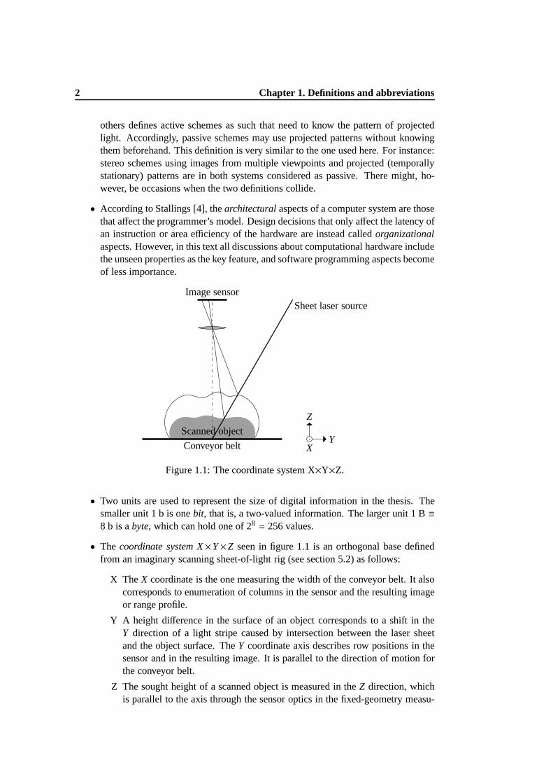
Figure 1.1: The coordinate system X×Y×Z.
• Two units are used to represent the size of digital information in the thesis. Thesmaller unit 1 b is onebit, that is, a two-valued information. The larger unit 1 B≡8 b is abyte, which can hold one of 28 = 256 values.
• The coordinate system X×Y×Z seen in figure 1.1 is an orthogonal base definedfrom an imaginary scanning sheet-of-light rig (see section5.2) as follows:
X The X coordinate is the one measuring the width of the conveyor belt. It alsocorresponds to enumeration of columns in the sensor and the resulting imageor range profile.
Y A height difference in the surface of an object corresponds to a shift in theY direction of a light stripe caused by intersection between the laser sheetand the object surface. TheY coordinate axis describes row positions in thesensor and in the resulting image. It is parallel to the direction of motion forthe conveyor belt.
Z The sought height of a scanned object is measured in theZ direction, whichis parallel to the axis through the sensor optics in the fixed-geometry measu-

1.1. Concept definitions 3
rement setup shown in figure 1.1. TheZ coordinate is normal to the conveyorbelt.
1st exposure
6th exposure
Figure 1.2: An example of Graycode.
• Throughout this document the wordGray always relates to Graycode, also calledmirror code since the sequence for a bit of weight 2n is mirrored or folded after2n+1 sequential values. In contrast, a straight-forward binarycoded sequence isinsteadrepeatedafter 2n+1 sequential values. The main advantage of Graycodeto its conventional alternative is that the difference between two successive valuesalways constitutes a change in exactly one position. Figure1.2 illustrates a set ofGraycoded light volume projections.
The wordgrey is British spelling of a nuance somewhere on a straight line betweenblack and white. Grey image data is usually thought of as binary coded valuesrepresenting light intensity, and grey values may be but areusually not Graycoded.
• The scalable length unitλ is taken from Kang and Leblebici [5]. It is used in sca-lablecomplementary metal oxide semiconductor(CMOS) design rules and relatesall lengths in a layout to half the minimum drawn gate length allowed, in a cer-tain process. The examples in this document use MOSIS scalable CMOS designrules revision 7.2 with additionalπ/4 rad angles. These rules do not hold in deep-submicron processes but are good enough for area approximations. For example,in a 0.8 µm process 1λ translates to 0.4 µm.
• Figures A.2 and A.3 show example CMOS layouts. For simplicity no substrateorwell contactsare explicitly shown andn- or p-typeselect layersare not drawn. Infigure A.2 all diffusions are ofn-type and in figure A.3 all p-type channel metaloxide semiconductor(PMOS) transistors are drawn within ann-well.
• Everywhere it occurs in the text, the phrasevisible lightrepresents electromagneticradiation residing roughly in the wavelength spanλ = c
ν∈ [400 nm, 700 nm], corre-
sponding approximately to frequencies in the intervalν = cλ∈ [430 THz, 750 THz].
When light is said to beinfrared in this document, mainly wavelengths in the inter-valλ ∈ ]700 nm, 1100 nm] are intended. Correspondingly,ultraviolet lightexhibitswavelengths shorter than 400 nm. This categorisation is a combination between hu-man colour perception and sensitivity of a silicon based electrooptical device suchas the CMOS sensor.
• The abbreviationsMAPPandNSIPdescribe certain types of column parallel andpixel parallel image processing architectures, respectively. Both are architectures

4 Chapter 1. Definitions and abbreviations
fulfilling the criteria for near-sensor processing described later. MAPP and NSIPare described in more detail in subsections 7.1.1 and 7.1.2,respectively.
• In this document the expressionnear-sensor processingis used to describe dataprocessing directly within an image sensor array or with at least one-dimensional2
communication channels between the sensor elements and thedata processor. Near-sensor processing is not necessarily synonymous with applying the NSIP archi-tecture.3
• Phase-shifting, phase-stepping, fringe-shifting, andfringe-steppingare four diffe-rent expressions describing spatial phase movement of a structured light projectionof some sort, all indicating different step sizes. They are not treated separately inthis text, instead when step size is critical it is mentionedby value.
• In the following text where the termsmart sensoris used it refers to the definitionstated by Johannesson in [2] p. I-8:
“A smart sensor is a design in which data reduction and/or processing isperformed on the sensor chip.”
Or, in a more general form, within the sensor hardware. For a more in-depth studyof smart image sensors see for instance Åström [6].
• The termssnap behaviourand snapshot imagesare in this document used fordescribing an event that occurs during a period of time that is small enough sothat the action can be treated as instantaneous. The conceptis therefore relativeto issues such as motion. A snapshot image of a scenery is an image taken withso short integration time that features in the image are not blurred significantly bymotion in the scenery, as described by the resolution demands for the image.
• Laser speckleis temporally static ‘noise’ in the image that arises when coherentlight hits optically rough surfaces. It can be thought of as an interferometric patternof bright and dark areas. For more in-depth information regarding speckle and itscountermeasures, refer to for example Gabor [7].
• A temporalor sequentialcode is a pattern that changes in time. TheGraycodedlight sequencedescribed in section 5.7 is a good example of such a code.
A boundarycode is a pattern that occurs between two different patterns, such asthe line between dark and bright areas in the Graycoded lightsequence describedin section 5.7.
Consequently, a code that occurs on the borderline between two temporally chan-ging patterns of light is called atemporal boundary code.
2That is, column or row parallel.3Probably contrary to the belief of most readers.

1.2. Abbreviations 5
1.2 Abbreviations
2D Two-Dimensional3D Three-Dimensionala-Si:H Hydrogenated amorphous SiliconA/D Analogue-to-DigitalALU Arithmetic Logic UnitAM Amplitude ModulationAND logical ANDASIC Application Specific Integrated CircuitBGA Ball Grid ArrayBiCMOS Bipolar Complementary Metal Oxide SemiconductorBoL Beam-of-LightCCD Charge Coupled DeviceCDS Correlated Double SamplingCMOS Complementary Metal Oxide SemiconductorCPU Central Processing UnitCW Continuous WaveDC Direct CurrentDFT Discrete Fourier TransformDMD Digital Micromirror DeviceDSP Digital Signal ProcessorFM Frequency ModulationFoV Field of ViewFPGA Field Programmable Gate ArrayGLU Global Logic UnitGOR Global ORLCD Liquid Crystal DisplayLED Light Emitting DiodeLUT Look-Up TableLVDS Low Voltage Differential SignallingMAC Multiply ACcumulateMAPP Matrix Array Picture ProcessingNAND inverting logical ANDNESSLA NEar-Sensor Sheet-of-Light ArchitectureNLU Neighbourhood Logic UnitNMOS n-type channel Metal Oxide SemiconductorNOR inverting logical ORNSIP Near-Sensor Image ProcessingOR logical ORPE Processing ElementPLD Programmable Logic Device
Table 1.1: Abbreviations used in this thesis.

6 Chapter 1. Definitions and abbreviations
PLU Point Logic Unitp-i-n Diode junction with an intermediate layer of intrinsic siliconp-n Diode junction in doped siliconPM Pulse ModulationPMOS p-type channel Metal Oxide SemiconductorPN Pseudo Noise (modulation)Pvlsar Programmable and Versatile Large Size Artificial RetinaPWM Pulse Width ModulationROM Read-Only MemorySAR Synthetic Aperture RadarSICK IVP SICK IVP Integrated Vision Products ABSIMD Single Instruction, Multiple DataSIMPil SIMD Pixel processorSNR Signal-to-Noise RatioSoL Sheet-of-LightSRAM Static Random Access MemoryTFA Thin Film on ASICToF Time-of-FlightUV Ultra-Violet (light)VIP Video Image ProcessorXOR logical eXclusive OR
Table 1.1: Abbreviations used in this thesis.

Part I
Overview
7

CHAPTER 2
Contents
This document describes the efforts made to find a new way of solving an old problemin the fields of automation and robot vision, namely, the peception of depth. The workhas been directed by a set of guidelines presented in section2.2 that originate from di-scussions within the company financing this study, SICK IVP Integrated Vision ProductsAB1. The first part of this document provides an overview of 3D imaging schemes. Eachscheme is then processed in a bit more detail in part II, leading forward to an identifica-tion of some core issues regarding the choice of path to follow when suggesting solutionsto some of these issues. In part III an idea is conceived on howto meet the demands in adecent manner, and part IV contains a conclusion of the results, some directions for futurework, and a discussion about how this study was implemented.
2.1 Background
SICK IVP Integrated Vision Products AB started in 1985 as a spin-off from LinköpingUniversity, where an idea was developed about integration of high-performance imageprocessing power into a CMOS image sensor. The development of the MAPP architecturedescribed in subsection 7.1.1 led to a system for extremely fast acquisition of laser sheet3D profiles (See for instance Johannesson [2] pp. I-53–I-78). Today, the technology fromSICK IVP is based on improvements and enhancements of the original MAPP sensorarchitecture combined with laser sheet-of-light scanningfor 3D image acquisition. Thelatest sensor, the M12 sensor described by Johansson et alii[8] and Lindgren et alii [9],and used for example in the products Ranger M40/M50/C40/C50/C55 [10, 11, 12] ofSICK IVP, is capable of delivering more than 20000 triangulation profiles per second,each 1536 values wide.
There are some fundamental limits to the scanning sheet-of-light triangulation techni-que when striving for higher speed and higher resolution, for instance, realizing extremelyaccurate motion control during scanning of very small geometries. Another problem withlaser sheet-of-light measurement is that speckle becomes an issue when coherent light
1In this text called SICK IVP.
9

10 Chapter 2. Contents
sources are used on very small geometries, for example examining solder bumps onballgrid array (BGA) components. Laser speckle is temporally static and a small movementor variation in the measurement geometry blurs the speckle patterns, thereby, decreasingthe effects. Non-scanning snapshot measurements will however sample the speckle withalmost no movement and hence suffer more from speckle than, for instance, scanningmeasurement schemes.
The vision regarding a new line of SICK IVP products is to be able to acquire a full 3Dimage snapshot extremely fast and with sufficient resolution, with maintained accuracyand robustness of the measurement while avoiding demands onobject movement. Thisvision is why the snapshot 3D project was launched.
2.2 Conditions for the project
Find a way to implement a full-image ‘3D snap’ algorithm in a sensor architecture thatfulfills the following criteria:
• Enough data for a standard PC to be able to calculate a 3D imageshould be acquiredin short-enough time for the system to be accurately modeledas a single-imagesnapshot system. Multiple images may be used if acquired fast enough.
• There should be no or minimum scanning motion involved.
• Depth resolution should be at least 1µm, and spatial resolution of the sensor of atleast 512× 512 pixels.
• Field-of-view range between 50 mm× 50 mm and 1000 mm× 1000 mm.
• The sensor should be economically feasible to produce in volume, which meansthat a standard CMOS process of 0.35µm or possibly down to 0.18µm minimumchannel length should be sufficient, possibly also a-Si techniques.
• Throughput of at least 25 3D images per second with a reasonable amount of com-putational work left to do for an external PC.
2.3 Working methodology
The project is intended as a Master’s Thesis project of 20 weeks, including the completionof this document. Responsible for the work is the author, Björn Möller, supported at SICKIVP by Mattias Johannesson and Henrik Turbell regarding suitable imaging algorithms.Support has also been available from Johan Melander regarding sensor issues. Examinerof the Master’s Thesis at Linköping University is Dake Liu.
The initial idea was to study existing techniques for 3D imaging as well as suitablecircuitry and architectures for image acquisition and image processing. Combined withmy knowledge in CMOS design and advanced image sensors, the expected result wasa proposal for a 3D snapshot imaging equipment that minimizes the deviation from theproject goals. Sources used to collect information are suchas various Internet baseddatabases, library catalogues, patent databases, and journals on related subjects. Also, my

2.3. Working methodology 11
supervisors and other skilled employees at SICK IVP have been very helpful in findinginformation on the subject.
Given a successful 3D imaging scheme the second task would beto find a way ofaltering the sensor system, and in particular the architecture of SICK IVP CMOS sensors,in such a way that the behaviour of a new system can come as close as possible to the3D snap goals. Lacking a suitable 3D imaging scheme, more effort should be applied inidentifying and solving some problems related to the most suitable schemes. Decisionsduring the work process make the adaptation and produceability parts less important andinstead more energy has been given to study the schemes and finding general solutions totheir weaknesses.


CHAPTER 3
Goals for the project
Before digging into the details of existing 3D imaging schemes, a second thought on thecriteria listed in section 2.2 might be appropriate.
3.1 Main project goal
• Find a way to implement a full-image ‘3D snap’ algorithm in a sensor architecturethat fulfills the following criteria.
The goal is not to develop image acquisition algorithms but rather to evaluate the possi-bility of, and if possible a way of, developing hardware thatcan support such algorithms.
3.2 Snapshot behaviour
Snapshot behaviour, the capability of processing an entirescene within a limited periodof time sampled as if totally immobile, is a cornerstone of this work. If image acquisition,or rather light integration, takes for example 4 ms a movement in the object scenery ofonly 250µm/s will result in aY direction inaccuracy of 1µm. Light integration time islimited by the power of the light source and the sensitivity of the photodetector device,which in turn depends on light absorbing area and parasitic capacitance, among otherthings. In the extreme case, integration time is limited by the transient behaviour of thephotosensitive device, a fact that is obvious in the case of non-integrating devices.
• Enough data for a standard PC to be able to calculate a 3D imageshould be acquiredin short-enough time for the system to be accurately modelled as a single-imagesnapshot system. Multiple images may be used if acquired fast enough.
• There should be no or minimum scanning motion involved.
Of all the 3D schemes listed in this chapter, only the pulse scheme using modulatedtime-of-flight in section 5.14 gives the impression of having the ability to acquire a full3D image in real-time out of one image.Pulse modulation(PM) Time-of-Flight(ToF)
13

14 Chapter 3. Goals for the project
is on the other hand severely limited regardingZ resolution. Defocusing and interfero-metric schemes look rather promising from a snapshot behaviour point of view, since theyrequire only two or three images. Unfortunately they do require mechanical movementto manipulate focusing distance of the imaging system, which is in violation of the de-mand for no scanning motion and may limit the maximum acquisition speed. Controlof this movement is probably a bit easier than constant-speed scanning though, since theonly important value to control is an end position rather than the velocity of a continuousmotion.
3.3 Speed
High-speed applications is the most important niche for SICK IVP technology, moti-vating customers to turn to rather expensive and complex solutions when inexpensivehigh-quality low-speed alternatives exist.
• Throughput of at least 25 3D images per second with a reasonable amount of com-putational work left to do for an external PC.
In combination with the other goals this translates into slightly less than 6.6·106 resultingmeasurement points per second.Reasonable computational workmeans in practice lessthan or approximately equal to one floating-point multiplication per pixel value. Thismeans that height data may be linearly rescaled before decisions are made, however, thereis not enough time for spatial filters, correlation, rotation, or other more or less complexcalculations without the aid of extra, specialized hardware.
Throughput and snap behaviour both put constraints on lightintegration time, whichin turn sets demands on light power. For instance, to resolvean image into 512 stepsof depth without subpixling efforts requires at least 11 images taken using sequentiallycoded light described in section 5.7; one dark and one totally illuminated image for thres-hold calculation, and nine sequential Graycoded images allowing for 29 = 512 steps ofheight data. This gives each image capture about 3.6 ms available for light integration anddata processing without violating the 25 Hz frame rate. In order to achieve good enoughaccuracy it may be necessary to project a couple of inverted Gray images too. Also, theentire time of 40 ms available for measurement in terms of throughput demands is notavailable for image capturing in order for the measurement to be accurately modelled bysnapshot behaviour.
3.4 Z resolution
Resolution of measured height is the key feature of 3D acquisition schemes.
• Depth resolution should be at least 1µm.
This goes for the smallerfield of view(FoV) of (50 mm)2, where the interesting depth-of-view is around 5 mm.1 In applications using the larger FoV, interesting depth resolutionis around 1 mm, and depth-of-view is about 500 mm. In terms of PM ToF (section 5.14)
1This results in around 5000 steps of depth, or 13 b integer representation. Existing products from SICKIVP [11] are capable of delivering depth resolution down to 1/5120 of the available depth range.
3.5. X×Y resolution 15
1 µm is equivalent to a global timing accuracy of 6.67 fs or better, which is not possiblein practice in a 5122 pixel array, as stated in theX×Y resolution section. In reality, all PMToF schemes using more than one pixel will be limited to an accuracy in the neighbour-hood of a few centimetres, mainly due to signal skew in the pixel array. Interferometricschemes in section 4.2 and Moiré interferometry in section 5.6 are known to produce highdepth resolution over small variations of somewhat smooth surface structures. They sufferinstead from phase ambiguity when the surface shows discontinuities or steep changes,thus, violating the demand on surface quality independence.
3.5 X×Y resolution
As always in image acquisition and processing the core of thedevice is a two-dimensionalarray. In physical terms each element must be kept small and simple since its impact onthe total system is multiplied by the square of 1D resolution.2 Data communication wit-hin a sensor chip and out of it, as well as storage of temporal information in the sensor,also scales in this quadratic manner. For instance, 8 tiny bits of memory for each pixel ina 5122 pixel sensor equals a huge 2 Mb of total memory. Such a size is perhaps an accep-table quantity on a dedicated memory chip, but not on a chip shared with an image sensor,since the memory will have to coexist with the 262144 photosensitive cells as well as withanalogue readout circuitry,analogue-to-digital(A/D) converters, digital communication,and control logic.
• Spatial resolution of the sensor of at least 512× 512 pixels.
This requirement limits the available area per pixel, the complexity of each pixel, datadistribution, and global timing. A maximum total chip area of for example(22 mm)2,which is near the maximal area available in a recently used 0.35µm process, sets thetheoretical pixel size maximum to about
(
40µm)2, leaving a 760µm wide border for pads
and out-of-pixel electronics. For instance, if omitting photosensitive devices altogetherthe available area allows less than 20× (9µm)2 cells of static random access memory(SRAM) per pixel, excluding read/write and addressing circuitry.3 A large chip alsodemands good optics in order to project the scenery onto a diagonal of 30 mm (≈ 13/16
′′)with minimal distorsion. In addition, the yield of a large chip is generally lower than forsmaller ones, due to the distribution of defects in silicon wafers.
A conventional CMOS sensor makes use ofp-n junctions near the surface of a siliconwafer. The same surface is also used for active components such as transistors. Also,routing of signals and power is made with opaque metals at higher layers placed on top ofthe silicon. Having electronic circuitry such as memories,A/D converters, comparators,amplifiers, etcetera within the photosensitive area interferes with imaging functionalityin a number of ways. For instance, metal wires occlude photo devices andp-n junctionsin the vicinity attract photon induced charges, thus, preventing detection in the photodevice as well as inducing noise in the interfering circuitry. These effects combined areconsidered in the so-calledfill factor, which is the equivalent percentage of the total pixel
2Image sensor arrays often use quadratic or rectangular arrays of around 1000 rows or columns, and thenumber is expected to increase.
39 µm is a reasonable size for an SRAM cell in a 0.35µm process, according to the author’s experience.

16 Chapter 3. Goals for the project
area detecting light in a sensor. The higher the fill factor, the higher the sensitivity ofthe sensor. Sensitivity is one limiting factor of spatial resolution, since it sets a practicalminimum energy of light. Putting photosensitive devices ontop of the metal layers usingthe technology described in section 7.2 and by Rantzer [13],Lulé et alii [14] amongothers, enables a fill factor close to 100 % even when the sensor array contains complexelectronic circuitry. The use of microlens structures as described in section 7.6 on top ofthe device is another way of improving the optical fill factor.
3.6 Communication requirements
[x-1, y-1]
[x-1, y]
[x-1, y+1]
[x, y-1]
[x, y]
[x, y+1]
[x+1, y-1]
[x+1, y]
[x+1, y+1]
a. 4-pixel neighbourhood
[x-1, y-1]
[x-1, y]
[x-1, y+1]
[x, y-1]
[x, y]
[x, y+1]
[x+1, y-1]
[x+1, y]
[x+1, y+1]
b. 8-pixel neighbourhood
[x-1, y-1]
[x-1, y]
[x-1, y+1]
[x, y-1]
[x, y]
[x, y+1]
[x+1, y-1]
[x+1, y]
[x+1, y+1]
c. 12-pixel neighbourhood
Figure 3.1: Complexity of communication between pixels.
The requirement onX×Y resolution discussed previously indirectly means that thereis no way of implementing complex global one-to-one communication between arbitrarypixels. What can be achieved is communication within a neighbourhood of around fourpixels as shown in figure 3.1 or a wired-gate structure of one bit per pixel forming pri-mitive global operations such as global OR, along with column- or row-parallel readout.Also, an asynchronous rippling global-context operation like the NSIPglobal logic unit(GLU) (see subsection 7.1.2) is possible.4 Complex calculations on global data such
External dft processorImage sensor
External memory
Output
Figure 3.2: Separate DFT processor.
as Fourier transformations and stereo image correlation seem unlikely to be completelysolved using only near-sensor processing capacity, due to the demand of memory andcommunication (see for example Johannesson [2] p. II-67). They are instead rather wellsuited for architectures using separate image sensors and astand-alonedigital signal pro-cessor(DSP).
4Time must be given for such an operation to complete since gate depth is in the order ofk · (X + Y),wherek is the gate depth per pixel. Acceleration techniques are notapplicable due to the regular and highlyarea optimized array structure.

3.7. Field of view 17
3.7 Field of view
This requirement mainly affects the choice of optics and light source. There are economi-cal limitations regarding optics and light sources that must be examined when developinga commercially acceptable product.
• Field-of-view range between 50 mm× 50 mm and 1000 mm× 1000 mm.
The smaller field-of-view, with 5 mm depth range, is intendedfor use in the field ofelectronics where depth resolution of a singleµm is used. Whereas, the larger one is ty-pically used in wood processing applications with a depth of500 mm resolved into 1 mmsteps. In other words, a field-of-view between(512×512×5000) × (100×100×1) µm3
and(512×512×500) × (2×2×1) mm3.The choice of light source and projecting optics is highly dependent on the field-of-
view of the application. The greater the depth, the higher the demand on power of the lightsource. Also, a scenery near the sensor combined with a wide object makes the anglesfor projection and viewing large, measured from the opticalaxis. This requires nonlinearmodels and makes aberrations in the lenses more severe and occlusion more pronouncedwhen using active illumination. In addition, light is attenuated in the viewing lens de-pending on the angle of the incident lightρ as cos4 ρ, according to Horn [15] p. 208 andJohannesson [2] p. I-14.
3.8 Production feasibility
• The sensor should be economically feasible to produce in volume, which meansthat a standard CMOS process of 0.35µm or possibly down to 0.18µm minimumchannel length should be sufficient. The possibility of using diodes in a-Si techni-que also exists, although this can not be considered economically feasible today.
This requirement limits very strongly what can be done within one pixel in a 5122 pixelarray. Utilization of a-Si is described in section 7.2. At present it seems far from aneconomically feasible solution but given time and researchefforts it may very well be arealistic alternative in the near future. Due to the long-time nature of development effortsinvolved forming an entirely new product branch both present and probable near-futureoptions must be considered.
Traditionally, volume production at SICK IVP AB has been around 102 – 104 unitsper year. In general, large volumes of CMOS circuits are in the order of 106 – 108 unitsper year. An example of products that are not produced in volume is equipment for pro-duction test for a specific unit, where a very small number of at most 10 units are built.The significance of production volume is in the trade-off between design and develop-ment costs and costs of fabrication and manufacturing. Whenconsidering a high-volumeproduct, inexpensive components and highly automated manufacturing are more impor-tant for the price per unit than the design cost. When building five units small resourcesare spent on automation and the materials of one unit can be a large part of the totalcost. Production of some thousand units per year is regardedas moderate volumes, whereper-unit costs as well as per-design costs are significant.

18 Chapter 3. Goals for the project
Regarding CMOS process dimensions, the cost of masks and fabrication usuallyincreases with decreasing feature sizes. On the other hand,circuits become smaller andtherefore each produced wafer results in more chips. Also asmentioned in section 3.5,due to the distribution of defects in CMOS chips smaller circuits contain less defects. Intotal, the most productive strategy is often to use as small feature sizes as possible. Goodimage sensor processes5 have usually been one or two generations behind the smallestcommercially available channel lengths for digitalapplication specific integrated circuits(ASICs). The ground for analogue and mixed-signal design seems somewhat unstablefor geometries smaller than 0.18µm (see for instance Paillet et alii [16] p. 4, Kleinfel-der et alii [17], Wong [18]), since leakage currents and other issues tend to sabotage theintended analogue behaviour of circuits. Some sources evenstate that analogue designsdo not scale at all with minimum channel lengths below 0.18µm. Also, the higher do-ping levels needed in newer processes constitute obstaclesfor photo detection, since thedepletion region of thep-n junctions normally used for photo detection decrease withincreasing doping levels. This decreases the volume where photon generated charges aredetected and also increases both dark currents and parasitic capacitances.
Devices like the Photonic Mixer Device, Photomischdetektor, or PMD, described byJusten [1], Luan [19], and Schwarte et alii [20], among many others, probably need spe-cially optimized fabrication lines in order to produce goodquality units. The whole ideaof the CMOS image sensor business is to make use of normal electronic device processesin order to reduce fabrication costs and provide a means for integrating electronics onthe sensor chip, contrary to thecharge coupled device(CCD) business, where processoptimization is dedicated entirely to imaging properties of the device.
3.9 Object surface dependence
All techniques require some optical properties of the studied objects. Requirements like‘enough light must be reflected back to the sensor’ are difficult to avoid since the sensoris dependent on photon flux, fortunately, they are rather easy to obey since a simplelight bulb often solves the problem.6 However, some schemes demand properties likesmoothness in shape, colour, or reflectance. A commerciallyacceptable product cannot rely mainly on such properties in order to work; otherwise the field of applicationswill be too narrow. Interferometric and Moiré schemes can not solve phase ambiguitiessingle-handedly if a step or crack splits a surface because the measured height at a pointis given relative to neighbouring measurements with a rather short unambiguity length.Hence, such techniques need to be combined with a more robust, absolute measuringone in order to give accurate and absolute measurements, like in Wolf [21] and Wolf[22] where phase-shifting fringe projection is combined with a Graycoded light sequencein order to overcome problems regarding relative measurement. Focusing, passive, and
5That is, CMOS processes that have been used for photoelectric applications of some sort and/or aresomewhat characterized in terms of photosensitivity. Rantzer [13] (paper IV, pp. 77–82) shows an exampleof what is in image sensors clearly a defect but has never beenconsidered, not even known, in other CMOSapplications.
6The number of photons detected in the sensor is a product of light source intensity, reflectance anddirection of reflected light from the surface of the object, aperture area of viewing optics, fill factor andquantum efficiency of the pixels, and time of exposure or integration time.

3.10. Detection of surface properties 19
shading schemes depend highly on surface properties. The first two require the presenceof recognizable objects and the latter assumes that the reflectance properties are constantover the surface. Use of individual thresholds as describedby Trobina in [23] stronglysuppresses the surface dependence of a measurement scheme.
3.10 Detection of surface properties
In previous SICK IVP sensors the ability to produce 2D greyscale values has been moreor less ‘in the package’, since grey values of some resolution, from one bit up to eightbits, have been used in determining the position of a laser stripe. Colour filters have alsobeen available in some applications. This may not be the casein a future technology usingextremely specialized 3D snap sensors. In its true sense, a height imagez(x, y) is not a3D image but rather two-dimensional information about the third dimension. Whether2D greyscale images are so important as to motivate implementation of specific hardwarefor the sole purpose of acquiring them must be answered in consideration of possibleapplications. The answer yes implicates further questionslisted below.
1. Is being able to choose between aquisition of depth information and of greyscaleimages a sufficient solution, or is so-called registered image acquisition necessaryas defined by Justen in [1] p. 17?
2. Do we need eight bits of resolution in the 2D image?
3. How fast should 2D images be output?
For the needs of SICK IVP regarding 3D snap imaging, greyscale images are not neededfor other reasons than perhaps validation of range data. A two-dimensional ‘depth map’z(x, y) is sufficient for this project, although, the possibility of greyscale image acquisitionwould provide an advantage to the sensor.


Part II
3D imaging schemes
21


CHAPTER 4
General 3D image acquisition
This chapter provides an overview of 3D measurement schemes. In order to achieve aclear view of what is out there in the whole field of 3D imaging Ihave accepted almostany source of information as long as I can understand the language1. The initial catego-risation of schemes, as exemplified in figure 4.1, is taken almost entirely from Schwarte[24], where all 3D imaging measurements are divided into triangulation described in sec-tion 4.1, interferometry in section 4.2, and time-of-flighttype methods in section 4.3.The subdivision of schemes in the three categories into the two types active and passiveschemes is also inherited from Schwarte [24].
3D imaging
Triangulation Interferometry Time-of-flight
Focus
Structured light
Passive Shading
Multi-wavelength
Holographic
Speckle
White light
Pulse
CW
PN
Figure 4.1: Overview of 3D imaging schemes.
4.1 Triangulation schemes
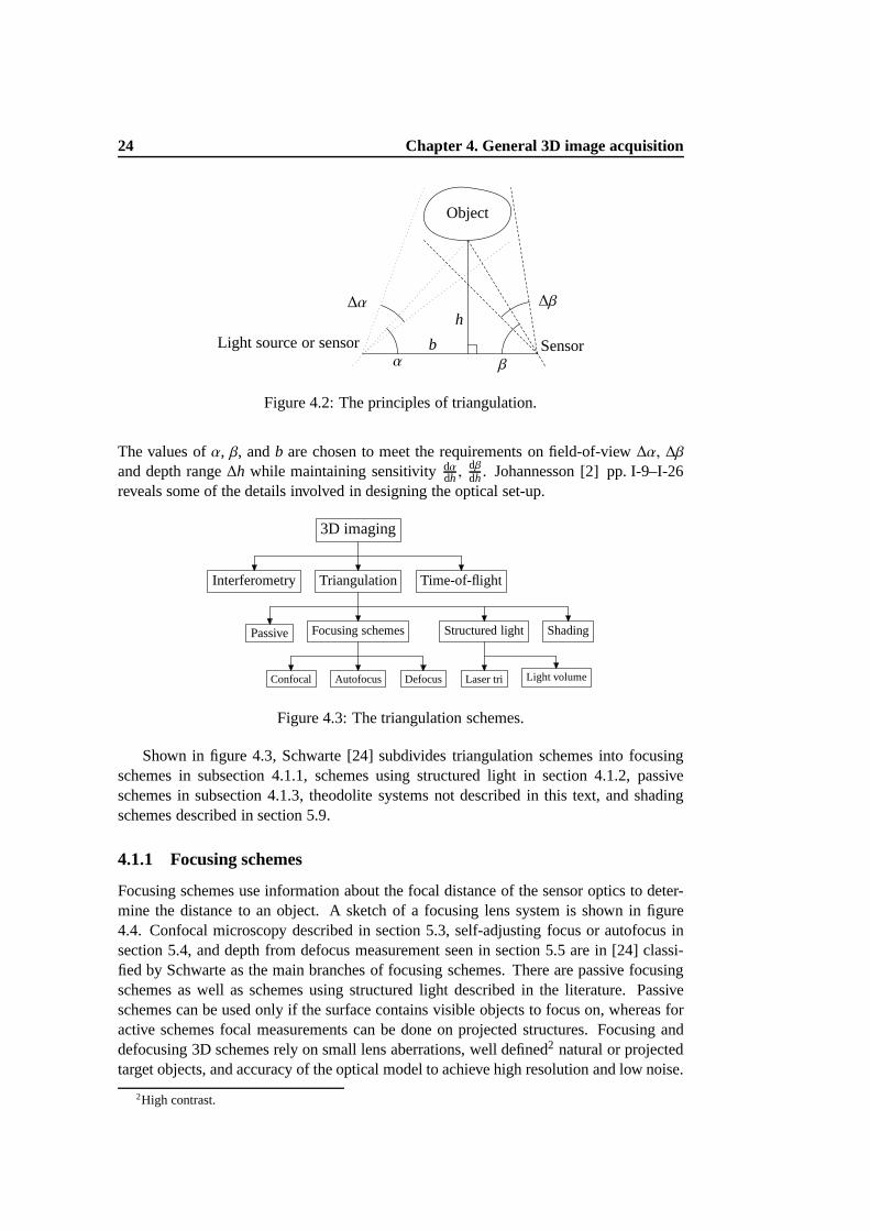
Triangulation makes use of 2D projection of one plane of light onto an object surfaceseen in another, non-parallel plane to determine distance.The principle of triangulationis described for example by Luan [19] pp. 5–7, by Johannesson[2] pp. I-3–I-8, and infigure 4.2. Knowing the values ofα, β, andb, the distanceh can be calculated as
h =b · sinα · sinβ
sin(α + β)(4.1)
1In practice this means that sources written in other languages than Swedish, Norwegian, Danish, English,or German are unavailable.
23
24 Chapter 4. General 3D image acquisition
α
∆α
β
∆β
h
b
Object
Light source or sensor Sensor
Figure 4.2: The principles of triangulation.
The values ofα, β, andb are chosen to meet the requirements on field-of-view∆α, ∆βand depth range∆h while maintaining sensitivitydα
dh ,dβdh. Johannesson [2] pp. I-9–I-26
reveals some of the details involved in designing the optical set-up.
3D imaging
TriangulationInterferometry Time-of-flight
Focusing schemes Structured lightPassive Shading
Confocal Autofocus Defocus Laser tri Light volume
Figure 4.3: The triangulation schemes.
Shown in figure 4.3, Schwarte [24] subdivides triangulationschemes into focusingschemes in subsection 4.1.1, schemes using structured light in section 4.1.2, passiveschemes in subsection 4.1.3, theodolite systems not described in this text, and shadingschemes described in section 5.9.
4.1.1 Focusing schemes
Focusing schemes use information about the focal distance of the sensor optics to deter-mine the distance to an object. A sketch of a focusing lens system is shown in figure4.4. Confocal microscopy described in section 5.3, self-adjusting focus or autofocus insection 5.4, and depth from defocus measurement seen in section 5.5 are in [24] classi-fied by Schwarte as the main branches of focusing schemes. There are passive focusingschemes as well as schemes using structured light describedin the literature. Passiveschemes can be used only if the surface contains visible objects to focus on, whereas foractive schemes focal measurements can be done on projected structures. Focusing anddefocusing 3D schemes rely on small lens aberrations, well defined2 natural or projectedtarget objects, and accuracy of the optical model to achievehigh resolution and low noise.
2High contrast.

4.1. Triangulation schemes 25
Sen
sor
outo
ffoc
us
Foc
used
obje
ctim
age
Optical axis
Thin lens
Obj
ects
urfa
ce
Defocus
Foc
alle
ngth
f
Figure 4.4: The principles of focusing.
For the basic principles of focusing in camera systems, refer to for instance Pedrotti andPedrotti [25], section 6.3 pp. 125–129.
4.1.2 Schemes using structured light
3D imaging using structured light means that a pattern of some sort is projected onto theobject surface by some kind of light source. The projection is then captured as an imageand analysed to extract the wanted information. A number of schemes are presentedby Schwarte [24] as triangulation schemes based on structured light, for example lasertriangulation, Moiré, and Graycoded light. Other schemes listed under focusing schemes(subsection 4.1.1) and passive schemes (subsection 4.1.3)also benefit from the use ofstructured lighting. Three different types of structured light are sorted out depending onthe dimensions of light. They are beam-of-light (see section 5.1), sheet-of-light (section5.2), and light volume techniques. The first two types use point-type and line-type laserbeams, respectively.3 The third category is interesting from a snap point of view since ituses projection of two-dimensional light patterns onto theobject surface. This means thatthe entire scene is illuminated by the structured light at the same time, in contrast to thefirst two kinds where only a very small portion at a time is lit by the laser source.
One interesting light volume scheme is the so-called sequentially coded light schemein section 5.7, where a sequence of different patterns is projected onto the target andsampled by an image sensor. Attempting to reduce the sequence of projections one couldturn to colour coding where instead of projecting different patterns in sequence a numberof illumination stages can be put into one single frame by using different colours of light.The sensor must then be able to separate colours well enough to extract the needed infor-mation. Also, the transfer function from colour pattern projector via the studied objectand through the colour sensor must preserve the projected colour.
3Point-type cross section of a laser beam and line-type crosssection of a laser plane.

26 Chapter 4. General 3D image acquisition
Different scenes put different restrictions on the type of pattern used in structuredlightapproaches. Hall-Holt and Rusinkiewicz [26] list three types of necessary assumptions,reflectivity assumptions like preserving colour information, assumptions onspatial co-herencemeaning that spatial neighbourhoods of image elements consist of neighbouringparts in the used light pattern as well as in the physical surface, andtemporal coherenceassumptions about maximum velocity of objects in the scene.
4.1.3 Passive schemes
3D scene
2D image
2D image
Z0
Z1 Z2Z3
Z′0 Z′1Z′2 Z′3
Z′′0 Z′′1 Z′′2 Z′′3
Figure 4.5: Stereo depth perception.
Three different schemes of 3D imaging are listed in the category of passive schemesby Schwarte [24]. All three are stereo based photogrammetryschemes using either several2D cameras in a known relative geometry (subsection 5.8.1),several 2D cameras withdynamic self-adjustment (subsection 5.8.2), or just one self-adjusting 2D camera takingseveral images in a scan-type manner (see subsection 5.8.3). Also, Faubert [27] describesthe motion parallax phenomenon (subsection 5.8.4). Commonto all four schemes is thebasic problem of comparing and correlating objects seen in different images from differentpoints of view. There does not seem to be a method to locally solve this problem withoutusing sequences of structured light. Stereo based schemes benefit greatly from the use ofstructured light, which in turn creates good criteria for solving the much simpler problemsof light volume techniques described in subsection 4.1.2.
3D imaging using stereo based sensors requires global correlation of details eithernaturally present in the object surface or projected onto it. A sensor with column paral-lel or pixel parallel processing of local properties is inadequate in terms of completelysolving the 3D measurement using general stereo vision, butin section 5.8 a number of

4.2. Interferometric schemes 27
Feat
ure
extra
ctin
gim
age
sens
or
Feature extractingimage sensor
Object
Feature correlation
Standard PC
Figure 4.6: Stereo camera with two image sensors.
schemes are presented solving the stereo problem confined torows4 or even single pixels.As shown by Petersson [28], an NSIP sensor might be useful as afirst step to process thescenery since it enables fast feature extraction. Still a separate processing unit such asa DSP is required to correlate features in the separate images and calculate depth. Sucha system, illustrated in figure 4.6 working with standard image sensors would need tohandle two parallel streams of say 53 Mb/s, calculated using 25 images per second with512×512 pixels of 8 b image data. In section 7.4 the communicationproblem is discus-sed. A reasonable amount of memory for the DSP would be able tostore a few entireimages, that is, in the order of 1 MB.
4.2 Interferometric schemes
3D imaging
Triangulation Interferometry Time-of-flight
Multi-wavelength Holographic Speckle White light
Figure 4.7: Interferometric schemes.
There is a wide range of interferometry applications, from microscopes describedfor instance by Notni et alii [29], viasynthetic aperture radar(SAR) by for exampleChapman [30], to deep-space interferometry by for instanceJPL [31]. Of course, in atypical SICK IVP application the first is the most relevant area.
4Or columns if it is more convenient.

28 Chapter 4. General 3D image acquisition
Laser source
Beam splitter
Object
Tuneable attenuator
Variable phase stepper
Beam mixer/collimator
Sensor
Figure 4.8: A typical interferometry setup.
The principle of optical interferometry is to make two lightbeams interfere, of whichone has travelled a fixed distance and the other is lead in a path, the length of which isdependent on the shape of a studied object surface. When the two images coincide afringe pattern occurs, which is dependent on the wavelengthand phase difference of thetwo light rays. For details on the basics of interferometry,refer to for example Pedrottiand Pedrotti [25], chapter 11 pp. 224–244.
There are numerous different interferometer set-ups: Fabry-Perot, Fizeau, Keck,Lin-nik, Mach-Zehnder, Michelson, Mirau, Twyman-Green, Young, etcetera. How to chooseinterferometry set-up is an issue of system design and is nottreated in this project. Com-mon to all interferometers, including Moiré types described in section 5.6, is that oneneed at least three images with different phase in order to measure absolute distance un-ambiguously, using some sort of phase manipulating as described in subsection 4.2.1. In-terferometers using multiple wavelengths (see section 5.11) and white light (section 5.13)solve the ambiguity problem in the first case by producing a longer synthetic wavelengthand in the second case by scanning the scene in theZ direction. Luan [19] pp. 7–8 andHeinol [32] pp. 8–9 classify optical interferometry as a ‘coherent time-of-flight’ method.
Interferometry using light of wavelengthλ can yield very high depth accuracy in theorder ofλ/100.
4.2.1 Phase-shifting
Phase or fringe shifting [21, 22, 33, 34] consists of moving agrating or light beam byfractions of a period in order to achieve more accurate measurements between fringes.Shifting the projection between at least three positions also determines the local order offringes; that is, it is determined without ambiguity whether a slope is downhill or uphill.5
5Provided that the maximum frequency is not violated anywhere in the scene.
4.3. Time-of-flight schemes 29
In the case of sinusoidally changing grey levels of light, phase shifting enables calculationof exact phase in a point, regardless of the surface properties in that point.
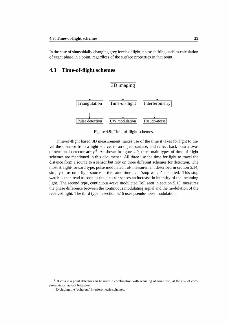
4.3 Time-of-flight schemes
3D imaging
Triangulation InterferometryTime-of-flight
Pulse detection CW modulation Pseudo-noise
Figure 4.9: Time-of-flight schemes.
Time-of-flight based 3D measurement makes use of the time it takes for light to tra-vel the distance from a light source, to an object surface, and reflect back onto a two-dimensional detector array.6 As shown in figure 4.9, three main types of time-of-flightschemes are mentioned in this document.7 All three use the time for light to travel thedistance from a source to a sensor but rely on three different schemes for detection. Themost straight-forward type, pulse modulated ToF measurement described in section 5.14,simply turns on a light source at the same time as a ‘stop watch’ is started. This stopwatch is then read as soon as the detector senses an increase in intensity of the incominglight. The second type, continuous-wave modulated ToF seenin section 5.15, measuresthe phase difference between the continuous modulating signal and the modulation of thereceived light. The third type in section 5.16 uses pseudo-noise modulation.
6Of course a point detector can be used in combination with scanning of some sort, at the risk of com-promising snapshot behaviour.
7Excluding the ‘coherent’ interferometric schemes.

CHAPTER 5
3D image acquisition schemes
This chapter consists of a list of possible 3D acquisition schemes. Each scheme is descri-bed in short, then its properties are weighted into a conclusion about the scheme.
5.1 Beam-of-light triangulation
Projected height
Laser beam source
Object height
Obj
ect
Sensor
Figure 5.1: The principles of beam-of-light triangulation.
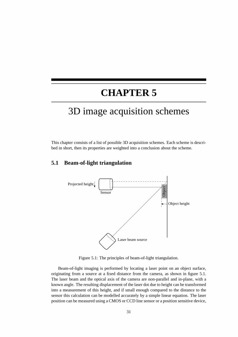
Beam-of-light imaging is performed by locating a laser point on an object surface,originating from a source at a fixed distance from the camera,as shown in figure 5.1.The laser beam and the optical axis of the camera are non-parallel and in-plane, with aknown angle. The resulting displacement of the laser dot dueto height can be transformedinto a measurement of this height, and if small enough compared to the distance to thesensor this calculation can be modelled accurately by a simple linear equation. The laserposition can be measured using a CMOS or CCD line sensor or a position sensitive device,
31

32 Chapter 5. 3D image acquisition schemes
described by for instance Johannesson [2] pp. I-37–I-38 andFujita and Idesawa [35]. Thesignal-to-noise ratio(SNR) of the measuring system can be improved by the choice oflight wavelength1 and using corresponding optical bandbass filters. Also, onecan usebackground adapted thresholds to find a laser dot or stripe.
Beam-of-light triangulation requires 2D scan and when measuring an entire sceneas sampled instantaneously the scheme is entirely inferiorto sheet-of-light triangulationdescribed in section 5.2, which is SICK IVP standard today. Scan time can be limitedthough if only a small portion of the scene is to be measured. Also, the 1D detec-tion principle allows for simpler detector structures than2D arrays. Since the conceptof beam-of-light triangulation is similar to sheet-of-light, no further discussion of thisscheme will take place.
5.2 Sheet-of-light triangulation
Projected height profile
Laser sheet source
Obj
ecth
eigh
tO
bjec
t
Sensor
Laser plane normal
Camera view
Figure 5.2: The principles of sheet-of-light profiling.
The sheet-of-light projection 3D measurement scheme is currently used by SICK IVP[2, 11, 36]. A fixed geometry is preferred, where the angle between the optical axis of a2D sensor and the direction of a laser plane is known, for example π/6 rad. The angleis a trade-off between sensitivity and maximum depth of the FoV. The stripeprojectedover the object surface is detected, and itsY position yields a height profile of the cutbetween the laser sheet and the object surface, as seen in figure 5.2. To view a full 3Dscene, a scanning movement is required in theY direction, either by changing the laserangle with a rotating mirror or in the case of fixed geometry bymoving the target. Usingfixed geometries simplifies calculation efforts when the measured raw data is translatedinto world coordinates.
1A CMOS image sensor responds to different wavelengths with varying efficiency and spatial accuracy.Also, there may be laws regulating the effect of lasers with certain wavelengths and the price for a lasersource differs for different wavelengths. Furthermore, structured light is more easily detected if it differsin colour from the main background source thereby effectively attenuating the main noise source in opticalfilters.

5.2. Sheet-of-light triangulation 33
SICK IVP makes use of the MAPP architecture described in subsection 7.1.1 for fastacquisition of laser profiles. EachX position (column) in theX×Y sensor has its ownprocessor and by sweeping theY address (row number) searching for a diffuse reflectionof the laser light itsY position2 is registered and output to an external PC through ahigh-speed serial interface. The main target in this project is to find a substitute tolaser sheet-of-light scanning in order to perform 3D measurements beyond the inherentlimitations of sheet-of-light triangulation.
Davis et alii [37] propose a unifying theory wheresheet-of-light(SoL) triangulationas well as sequentially coded light in section 5.7 can be treated as special forms of stereoschemes as described in section 5.8.
Curless and Levoy [38] present a, probably rather slow, way of improving accuracy ofbeam-of-light(BoL) and SoL calledSpacetime Analysis. Usually a sheet-of-light rangescanner searches through a column in the sensor array for a spatial position of a lightstripe. The finite width of the stripe is reflected from the object surface and is therebydistorted by the shape and reflectance variations of the surface. This results in a rangeerror due to deformation of the intensity profile of the sheet-of-light cross-section.3 Ins-tead, spacetime analysis processes the temporal variationof intensity from a point on thesurface during the scan. The width and position of this variation is in theory not depen-dent on reflectance properties or shape of the surface. Another advantage is that perfectlyregistered greyscale images are available at no extra cost.The biggest downside of spa-cetime analysis is that processing is performed along tilted lines4 in an interpolated 3Darray of greyscale data after a complete scan.5 This improvement is not of direct interestwithin the frame of this project both due to the massive amount of data processing andstorage needed, and because it is an enhancement to a scanning scheme.
SoL can also be performed using an inverted light scheme (seefor instance Bradshaw[3] p. 7) where a powerful, smooth, and approximately parallel beam source of whitelight is occluded for example by a narrow stick or wire, or even better by a sharp edgebetween light and dark, similar to the Graycode schemes described in section 5.7. Theresult is the same as using a laser sheet except that the lightis no longer coherent andmonochromatic and that it is the position associated with minimum intensity or maximumgradient, respectively, rather than with maximum light intensity that yields the rangevalue. Due to the use of incoherent light the ‘not light’ stripe will probably be a bit widerand more diffuse than the laser stripe. The advantages are mainly the lessexpensive lightsource, possibility of higher light power, and improved eyesafety.
As stated by Johannesson in [2] pp. I-6–I-7, the advantages of SoL ranging over forinstance Graycode schemes are that each acquired image holds enough information fora complete range profile, and that scanning the sheet-of-light is a much simpler problemthan the sequential projection of entire 2D images, among others.
Since beam-of-light and sheet-of-light schemes make use ofscanning motion they are
2There are numerous ways to interpolate the center position of a laser stripe from the shape of the reflec-tion. They are not discussed in this work since they are related to the technique to be replaced.
3The cross-section is usually assumed Gaussian and there is alarge number of algorithms for findingthe ‘center’ of the stripe. The error caused by a corner or step change in reflectance depends on the usedalgorithm, but can not be compensated for entirely.
4Straight tilted lines if the scan speed is fixed and known, bent curves if the scan speed varies in time.5In a typical SoL system each 2D greyscale frame is reduced to avector of range values before the next
frame is processed.

34 Chapter 5. 3D image acquisition schemes
not suited for this project.
5.3 Confocal microscopy
The sensor optics focuses on a fixed distance and determines whether the viewed partof the scene is in focus or not. The focused sensor distances is used as a measurementof height and is associated with the current area of the object surface if the criteria forin-focus are fulfilled. Confocal microscopes focus on only one surface point6 at a time.NanoFocus [39], for example, use a rotating disc of pinholesto scan through an objectpoint by point while shutting out interfering light from other parts of the scene. The lightsource in use yields to some extent white light.7 To measure an entire object requires anX×Y×Z-scan in focused distance. Perhaps a microlens structure could project one part ofthe scene onto one part of the sensor, thereby decreasing theextent ofX×Y×Z scanning.Parallelising the measurement in two dimensions means using a set of optics for eachsmall sensor portion with its own focus measurement electronics. Perhaps a structure likethesingle-instruction multiple-data pixel processor(SIMPil) by Cat et alii [40] would bebeneficial, having a processor connected to eachn×n subarray ofthin film on ASIC(TFA)pixels.
Chromatic aberration(see for instance Pedrotti and Pedrotti [25] pp. 102–104, canbe used to eliminate the focal scan using a colour sensor withgood enough colour separa-tion or using colour scans with controlled monochromatic light, such as a tuneable lasersource, provided that there are objects to focus on regardless of the colour of light. Themeasuring depth is then limited by the maximum chromatic aberration of a lens system.
Liu [41] describes in chapter 2 Image Focus Analysis as a means to solve the questionof focus. A part of an object surface will be best focused in atmost two sequentialimages achieved during a focus scan, so the scheme introduces no ambiguities regardingabsolute measurements. Focal scan step length determines depth resolution, which meansthat allowing for more images provides higher accuracy measurements at the expense ofspeed.
Johannesson ([2] p. I-20) defines an object to be in focus whenthe focusing ray-conehas a cross section width which is less than ½ pixel pitch. This also implies that spatialresolution of the sensor constitutes a limit for the accuracy of focus measurement.
The basic problem of focus measurements is the point spread function (Liu [41]pp. 38–42, Subbarao [42]), which states that the radius of animage corresponding toa point object depends on the amount of defocus of the point as
R=s · D
2·(
1f−
1u−
1s
)
, (5.1)
whereR is the radius of the blurred point,s is the distance from the lens to the detectorsurface,D is the aperture diameter,f is the focal length of the lens, andu the distancebetween the lens and the object point, as illustrated in figure 5.3. Assuming that theentire scene is located at the same distanceu, the spatial frequencies in the image are
6In this sense a point is a portion of the scene to which one single height measurement is assigned. Inreality it is a complete image containing high-contrast objects to focus on.
7White light in this context means using a light source with continuous spectrum showing a rather flatpeak reaching both red and blue.
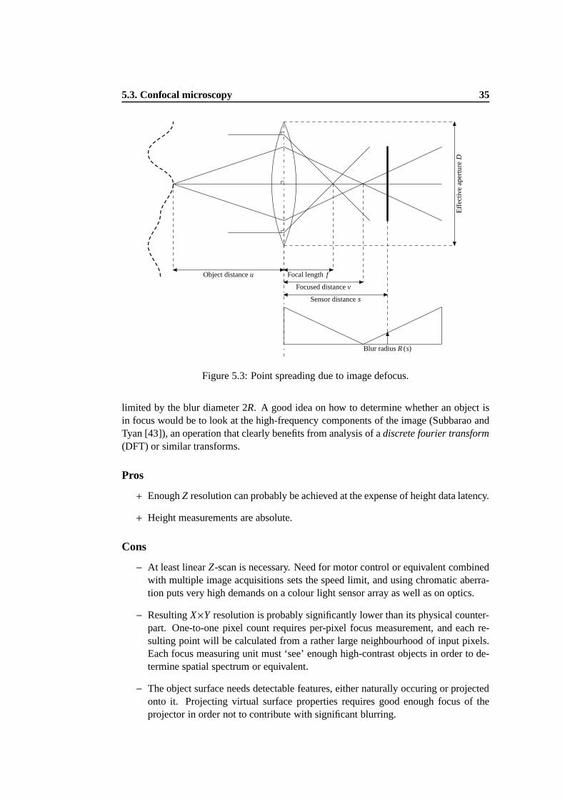
5.3. Confocal microscopy 35
Object distanceu Focal lengthf
Focused distancev
Sensor distances
Blur radiusR(s)
Eff
ectiv
eap
ertu
reD
Figure 5.3: Point spreading due to image defocus.
limited by the blur diameter 2R. A good idea on how to determine whether an object isin focus would be to look at the high-frequency components ofthe image (Subbarao andTyan [43]), an operation that clearly benefits from analysisof adiscrete fourier transform(DFT) or similar transforms.
Pros
+ EnoughZ resolution can probably be achieved at the expense of heightdata latency.
+ Height measurements are absolute.
Cons
− At least linearZ-scan is necessary. Need for motor control or equivalent combinedwith multiple image acquisitions sets the speed limit, and using chromatic aberra-tion puts very high demands on a colour light sensor array as well as on optics.
− ResultingX×Y resolution is probably significantly lower than its physical counter-part. One-to-one pixel count requires per-pixel focus measurement, and each re-sulting point will be calculated from a rather large neighbourhood of input pixels.Each focus measuring unit must ‘see’ enough high-contrast objects in order to de-termine spatial spectrum or equivalent.
− The object surface needs detectable features, either naturally occuring or projectedonto it. Projecting virtual surface properties requires good enough focus of theprojector in order not to contribute with significant blurring.

36 Chapter 5. 3D image acquisition schemes
− Transform domain or convolution approaches for focus measurement require mas-sive data communication in more or less global context.
Impression
∴ Focusing schemes work well on semi-global data in transformbased algorithms,and are better suited for camera systems using high output rate CCD or CMOSsensors with high spatial resolution in combination with discrete DFT and DSPunits as shown in figure 3.2. Confocal microscopy seems unable to meet the requi-rements for speed with minimal scanning, and requires sophisticated motor move-ment steering.
5.4 Self-adjusting focus
The self-adjusting focus or auto-focus scheme described byfor example NanoFocus inc.[44] is very similar to confocal microscopy in section 5.3, but in this case a focus measu-rement detector controls the focusing distancesof the lens so that the currently measuredregion on the object surface is always in focus. As all focusing schemes autofocus followsthe principles described in section 5.3. The distance to thesurface is simply calculatedfrom the measured angle of the screw-thread adjusting the lens. Basically, in this case thetask is to minimize the focusing errors− ν by changingsusing
s− ν =2 · R · ν
D, (5.2)
or, in the Fourier domain, changingsso that the energy shifts to higher frequenciesν.Unless a method is developed to focus the pixels of a two-dimensional sensor array on
arbitrary distances independently, self-adjusting schemes require anX×Y scan to measurea complete 3D scene. Perhaps the lens system developed by Philips [45] (see section 7.7)provides a step towards such a drastic improvement.
Pros
+ EnoughZ resolution can probably be achieved, provided that good angular measu-rement schemes are available.
+ No linearZ scan is necessary. There is however need for a large number ofexposu-res at different focusing distances searching for the right focus setting. In practiceat least logarithmic scanning might be needed.
+ Height measurements are absolute.
+ Best possible focused 2D grey values are available at no or little extra cost.
Cons
− Need forX×Y scan makes it very slow.
− The object surface needs detectable features, naturally present or projected, exactlyas confocal schemes in section 5.3.
5.5. Depth from defocus 37
Impression
∴ Autofocusing seems unable to meet the requirements of speedwith minimal scan-ning and requires sophisticated motor motion steering. Depth from autofocus is nota good candidate for a 3D snap sensor.
5.5 Depth from defocus
All focusing schemes follow the principles described in section 5.3. Schemes measuringdepth from defocus or out-of-focus blur use the fact that size8 (and hence also intensity) ofa spot out of focus depends on the distance to the object as seen in figure 5.3. The distanceu is obtained directly from or rather via a transform of the relationship of equation (5.3),
u =s
s/ f − 1− 2 ·R/D(5.3)
which is easily derived from equation (5.1). At least two different focus settingss arerequired, by turning the lens system with a stepper motor or by moving the sensor backand forth, for instance with a Piezo element.D and f are known by construction of themeasurement setup, and the problem of measuring depth translates into achieving goodenough approximations ofR. Gökstorp [46] pp. 59, 67 suggests that since focusing byadjusting the lens also affects the magnification, only the apertureD should be used tocreate blur in the image. Liu [41] states that depth from defocus is faster than focus scansince only two or three images with different focus are needed to extract depth infor-mation. It is instead less accurate, since measurements areextra- or interpolated froma few measured points. Both a spatial-transform domain method and a Fourier domainapproach are described.
Favaro [47] presents an approach with a ‘real aperture camera’, where a small numberof (at least two) images are taken from the same point of view but with slightly differentfocus. Nayar et alii [48] describe a system utilizing two CCDs and a pattern projector, allmounted in an optically coaxial fashion and using the same optics.
According to Liu [41] pp. 18–19, an unblurred imagef (x, y) can be obtained fromtwo blurred imagesg1(x, y), g2(x, y) from the inverse S transform by
f = g1 −σ2
1
4· ∇2g1 = g2 −
σ22
4· ∇2g2. (5.4)
The same source states that∇2g1 = ∇2g2, which, used in equation (5.4), gives
σ21 − σ
22 = 4 · g1 − g2
∇2gn, n ∈ {1, 2}. (5.5)
Combined with the knowledge that
σ1 =D1
D2· σ2 + k · D1 ·
(
1f1− 1
f2+
1s2− 1
s1
)
, (5.6)
8Equivalent to blur radiusR in figure 5.3.

38 Chapter 5. 3D image acquisition schemes
wherek is relating the statistical deviation parameterσ to a deterministic spot radiusR, we get a quadratic equation in eitherσ1 or σ2. It is not obvious thatk is constantover theX×Y plane, but such an assumption is necessary in order to justify acquisitionof the unknown parameter from calibration. As long as both images are known to betaken on the same side of the focused image, one solution in the quadratic equation caneasily be written off as false; otherwise one more image is needed to determine whichone is the true solution. Almost the same calculations are used in the Fourier domainapproach presented in Liu [41] pp. 16–18. A small enough Laplacian convolution kernelcould possibly be implemented in hardware in an NSIP type architecture for depth fromdefocus using the spatial domain approach described by Liu [41].
Pros
+ The need forZ-scan is reduced into taking at least two images with different focus.Motor control needs only place optics in two states, perhapsusing the liquid lensdescribed in section 7.7.
Cons
− Less accuracy compared to the schemes in sections 5.3 and 5.4.
− The object surface needs features of some sort, comparable to the scheme describedin section 5.3. Projecting virtual surface properties requires absolute focus of theprojector, regardless of the shape of the surface.
− Transform domain or convolution approaches for focus measurement require mas-sive data communication in at least semi-local context.
Impression
∴ Depth from defocus seems to be the most suitable one of the three focusing sche-mes, except forZ resolution. High-speed motor control for the focusing lensisnecessary, but only to move the lens between two or three fixedlocations. It is notobvious how to implement the Laplacian convolution in a parallel structure sinceit requires both computational and communicative, and probably also A/D conver-sion hardware, within the sensor array. Also, the scheme depends on high contrastimage objects.
5.6 Moiré
Moiré schemes can be regarded as triangulation schemes, as for example by Schwarte[24], or as interferometric schemes, like in Liu [49]. In this project there is no need foran absolute classification of the schemes. The idea of Moiré techniques is to let lightpass through gratings in two layers in the measurement. Oncebetween the light sourceand the object and once again before light from the object reaches the detector. Due tointerference of the two resulting wave patterns, fringes occur in the final image. These

5.6. Moiré 39
Object
Light source
Sensor
Projection grating
Viewing grating
Figure 5.4: The principles of Moiré.
fringes can be used as a measurement of the relative changes in height. A good overviewof different Moiré techniques is presented in [50].
Fringe projection schemes of all sorts like Moiré techniques making use of light withspatial intensity variations of a sinusoidal form benefit greatly from phase-shifting (seesubsection 4.2.1) to acquire sub-pixel accuracy. Without phase shifting, Moiré is reducedto counting fringe maxima and minima. This provided that thesurface properties do notchange too quickly in space, in other words all fringe positions are distinguishable. Forinstance, say that colouring of the object makes the surfacereflectance vary exactly as theinverse of the Moiré pattern. The image seen is a smooth grey screen without detectablefringes. If one such phenomenon can manage to conceal only one fringe, then fringe countwill show a step increase in deviation from the actual surface height at that position. Moreissues on the general concept of background light suppression are presented in section 7.8.
Projection Moirédescribed by Choi and Kim [33] uses a projection grating and aviewing grating with the same pitch. Light from the source passes the projection gratingfrom a lens, causing projected shadows on the object surface. The light is reflected fromthe object through the viewing grating and the resulting interference pattern is focusedonto a detector array.Shadow Moiréin for example Wang and Hassell [51] uses the samegrating for both projection and viewing. Light passing through the grating causes shadowson the object surface. The pattern of the reflected light passes the grating a second timebefore it hits the sensor. A Moiré technique called‘alternating Moiré’ is described byWolf [21] and Wolf [22] where a (perhapsliquid crystal display(LCD) based) deviceprojects stripes onto an object surface and the ‘dead zone’ between rows in the imagingcamera acts as a viewing grating. The pitch of projection grating and viewing gratingis not equal in this case. To achieve almost sinusoidal greyscale fringes for the Moirépattern the binary-valued liquid crystal stripes are brought slightly out of focus. Issueson different pattern projection techniques can be viewed in Wiora [34], and the topic isdiscussed in section 7.5.
When making use of Moiré techniques, spatial height changesin the object surface

40 Chapter 5. 3D image acquisition schemes
must be slow enough to make the frequency of resulting Moiré fringes much less thanthe frequencies of illuminating and viewing gratings in order for Moiré interferometry toyield height measurements of good certainty.
As described by Wolf [21] and Wolf [22] the four times phase shifted Moiré imagescan be combined with a Graycoded sequence (section 5.7) to turn the relative-measuringtechnique, which is otherwise very sensitive to surface discontinuities, into a robustabsolute-depth measuring pixelwise processable scheme. Wiora [34] also makes use ofGraycode sequences to enhance phase shifting of projected fringes. The Graycoded lightapproach requires in-focus stripes in the projector, so some kind of focus changing me-chanics is needed in the projector for measurements.
A four-image Moiré phase in a pixel position can be solved using equation (5.7),
ϕ(x, y) = arctanI4(x, y) − I2(x, y)I1(x, y) − I3(x, y)
, (5.7)
whereas five-point imaging, using redundant information intwo inclusive ends of theperiod in order to improve accuracy, is calculated as
ϕ(x, y) = arctan2 · (I4(x, y) − I2(x, y))
I1(x, y) − 2 · I3(x, y) + I5(x, y), (5.8)
according to Wiora [34] and Lam [52], and Choi and Kim [33], respectively. Anotherslightly more complicated solution is presented in equation (5.10) of section 5.11. Theimage valuesI i (x, y) = Γ(x, y) · (1+ M(x, y) · cos(ϕ(x, y) + i · ∆ϕ)) sample the scenery litby Moiré fringes of different shiftsi · ∆ϕ = n · π2 , n ∈ � andϕ(x, y) is the phase valuecontaining depth information. The constantΓ represents light intensity andM is modu-lation depth associated with the contrast of fringes. Accuracy of the scheme increaseswith increasing grating frequencies, however, it will not work at all if more than a smallfraction of a period in the resulting fringe pattern is seen by one single pixel. Violatingthe condition would result in a grey level average from this pixel, effectively cloaking allphase information there.
PPT Vision developed a scanning-mode fringe projection scheme called ‘ScanningMoiré Interferometry’ [53], where three lines in an image sensor array are used for samp-ling a scanned object at three different phase values of the projected pattern.9
Pros
+ High accuracy can be achieved, provided that good quality gratings are available ata reasonable cost.
+ The minimum requirement is only three exposures.
+ Measurements can be performed locally using only information available withinone pixel. Addition and subtraction can be performed in the analogue domain.
+ When using fringes projected from a projector based on LCD ordigital micromirrordevice(DMD) technique, no mechanically moving parts are necessary.10 Mosttechniques use some kind of movement, though.
9In September 2004 PPT Vision sold the SMI technology to Ismeca, according to for instance MachineVision Online [54].
10Actually, in the first case crystals are turning and in the second case small mirrors are moving.

5.7. Sequentially coded light 41
+ Greyscale images can be fairly easily acquired, for exampleby, averaging the va-luesI i .
Cons
− Height measurements from a pure Moiré scheme are relative. The surface must notcontain steps, cracks or other discontinuities. In order toallow for more generalsurfaces Moiré can be combined with other techniques, whichwill cost extra timeand hardware.
− An arctan(·) function is needed as well as a general grey level division. In the laterform also multiplication by 2 is needed, which is very easilyachieved in the digitaldomain. However, analogue-to-digital per-pixel grey level conversion is resourceconsuming and introduces fixed-pattern noise.
Impression
∴ Provided that a fast and small arctan(·) function can be implemented, four-phasestepping Moiré and similar projected-fringe techniques seem rather promising re-gardingX×Y×Z resolution and speed. Snap behaviour is compromised by theneed for multiple exposures and the relative measurement result must be comple-ted using an absolute measuring technique, for instance theone described by Wolf[21] and Wolf [22]. Phase-stepping Moiré schemes are interesting as part of thesolution to a 3D Snap sensor.
5.7 Sequentially coded light
1st exposure
2nd
3rd
4th
5th
6th exposure
Figure 5.5: A Graycoded light sequence.
First an image with only background light is averaged with animage where the entireobject is lit. The result is then used as an array of pixel unique thresholds in the following

42 Chapter 5. 3D image acquisition schemes
sequence. This step is a method for background suppression,more of which is discussedin section 7.8. Next, half of the object is lit while the otherhalf is masked out from thelight source, like the first exposure in figure 5.5. The line separating the two areas canbe used in the same way as a sheet-of-light stripe (see section 5.2) to determine height ofthe object surface in that particular slice. Shaded pixels should have a light value underthe corresponding threshold thus yielding a binary zero, while pixels seeing the light halfof the scene experience values above their threshold and accordingly produce a binaryone. The pixel unique thresholds suppress static11 background light as well as spatialdifferences in reflectance of the object surface. The core of light volume techniquessuch as Graycoded light is the quality and performance of a structured light projector.Projection techniques are further discussed in section 7.5.
The next step is to project a light stripe onto the object so that each of the former partsof the scene is cut in half by a line separating light from dark. If the result from threshol-ding of the former image is interpreted as the most significant bit of the height value ineach pixel, the next result is the (Graycoded) second most significant bit. The sequenceis repeated until the desired height resolution is achieved.12 The difference between se-quence images and threshold values can be used as a measurement of significance in eachpixel. The greater the difference, the better the probability of a correct decision. A goodgrey image can be acquired by simply reading out the background adjusted thresholdvalues.
The procedure is illustrated in figure 5.5, where light patterns are numbered in se-quence of decreasing significance in the height code. Each illumination in the temporallyapplied sequence can be thought of as doubling the number of sheet pattern sources fromthe previous one with new, unique angles just like a mirror sweeping a sheet-of-lightsource across the object surface. Unfortunately, use of other light sources than lasermakes the stripes a bit more blurred in sheet-of-light triangulation. Also, as stated in[2] p. I-6, motion in the scene causes severe errors in the measurement result since asingle resulting image is created using multiple sequential exposures. The advantage ofGraycode to other coding techniques is that the error causedby movement within theclosest neighbourhood of a depth measurement is constrained to one least significantbit, whereas the maximum error for normal binary code is halfthe total depth range,provided that the surface is smooth in that neighbourhood. Trobina [23] describes onescheme using Graycoded light. The technique is also used forsolving phase ambiguitiesin [21, 22, 34] as discussed in section 5.6.
The reasons behind using Graycode instead of, for example, normal binary codemight be to minimize spatial frequency in the projector and avoiding difficult decisionsdue to the redundant stripes in the later case, among others.In an ideal world, using binarycoding would be equally effective, except that the projector would need to output twiceashigh frequencies as for Graycode with corresponding resolution. Some issues regardingdesign of general sequence codes are suggested by Hall-Holtand Rusinkiewicz [26]. Astructured method is described, where a sequence ofn images yields 2n possible temporalcodes. Between each of the
(
2n
2
)
possible pairs a temporal boundary code is found. After
11The term ‘static’ is determined totally by integration time. Temporal changes in light during integrationshould be negligible.
12Resolution reaches its limit when one single pixel sees morethan one border, or when the projector nolonger produces sharp stripes.

5.7. Sequentially coded light 43
removing some unwanted boundaries, a path is sought such that each ‘good’ boundaryis used twice, once in each direction, in order to produce a code of maximal length withgood properties. The result is a good alternative to the binary-tree type Graycode. Usingn = 6 frames, the number of ‘raw’ boundaries is 2016, suggestingthat fewer images areneeded than using Graycode. The tasks of discarding bad boundaries and finding optimalpaths could easily be implemented in software, although true optimization means veryheavy computational work. A stripe boundary code generatorwas implemented and thesource code is shown in appendix B. The results from the rather simple path search showthat of the 2016 raw boundaries the longest achieveable pathfor a stripe boundary codeis only 256 nodes.
As stated in section 5.2, Davis et alii [37] classify sequentially coded light projectionas a time-domain stereo scheme (see section 5.8 for details). A camera placed exactly asthe projector would see the projected pattern almost undistorted. At each position in thesequence the two images, the projected pattern and the imagetaken from the viewpointof the first camera, are treated as a stereo image pair in orderto extract depth information.The sequence of different patterns enables a unique match in pixel based stereo search.This is almost exactly the same case as described by Albrechtand Michaelis [55].
5.7.1 Colour coding
The temporal sequence of patterns used in Graycoded schemescan be made more com-pact using a colour sensitive image sensor. Zhang et alii [56] treat the three distinguisha-ble colours red, green and blue as more or less independent patterns, thereby making thenecessary temporal sequence length one third of its black and white equivalent.
In Zhang et alii [56] Graycode is however not used, instead a so-calledde Bruijnsequence is used. As stated in [56] p. 6,
“. . . ak-ary de Bruijn sequence of ordern is a circular sequenced0, d1, . . . , dkn−1,where each elementd j is taken from a set ofk values and for which any sub-sequence of lengthn appears exactly once.”
stacked diodes colour filter
Figure 5.6: Typical colour response using a) photon absorption depth and b) filter.
When making use of multiple colours there are a few details toconsider. First, the sensorshould be able to separate colour good enough. On the contrary most colour CMOSsensors have a high degree of cross-colour dependence, a coarse sketch of a typical RGBresponse is shown in figure 5.613. Second, the object surface must not distort coloursin the projected light. Last but not least, optics in the system must be free from colouraberrations.
13The filter response in figure 5.6 b is rather exaggerated.
44 Chapter 5. 3D image acquisition schemes
Pros
+ Suppression of differences in reflectance is possible using pixel unique thresholds.
+ Resulting height measurements are absolute.
+ The basic measurement calculations are almost identical tosheet-of-light triangu-lation, which is well known by SICK IVP today. The main difference is the ‘emu-lated laser sheet sweep’ behaviour instead of fixed geometrylinear object scan. Ifthe bundle of rays from the projector can be made parallel, this difference can alsobe avoided.
+ No moving parts are needed if the projector is built without moving parts. However,it might be difficult to find fast enough such projectors at a reasonable price.
+ The scheme is very suitable for NSIP type architectures, provided that a TFA de-tector technique is available. An analogue memory with an average-of-two option,a comparator and a digital 10 bit memory are enough to performper-pixel depthmeasurement. The output is a digital, Graycoded ‘laser profile’ image. The down-side with in-pixel A/D conversion is that read data is increased about ten times.Instead of reading out one analogue value per pixel a set of binary values must befetched. On the other hand, a digital line probably requiresless settling time thanan analogue one.
+ Grey values can be obtained by reading out the pixel unique thresholds.
Cons
− The technique requires a large number of images. For instance, two exposuresfor threshold calculations,n frames forn bits height resolution, and one or tworedundant exposures in order to limit errors. Each image capture is limited in timeto the longer of minimum integration time14 and projector settling time.
− As with most triangulation schemes, shadows from large height differences on theobject may occlude parts of the scene, resulting in missing values.
− The scheme is less accurate than sheet-of-light triangulation, mostly due to the lightsource and blurring of the mask edges from focusing limits ofthe projector. Also,motion in the scenery can not be compensated for as easily as in sheet-of-lighttriangulation schemes.
Impression
∴ The need for a large number of images with different light settings makes schemesusing only Graycoded light on largeZ scans violate the speed requirement of 25images per second, and also the snap behaviour is compromised. Light sequenceschemes are however very well adapted to NSIP architectures, and the principles ofmeasurement are very similar to the well-known sheet-of-light technique, of whichSICK IVP has long-time experience and knowledge.
14Integration time corresponds directly to the intensity of alight source.

5.8. Stereo vision 45
5.8 Stereo vision
All schemes based on stereo or optical disparity require image acquisition from at leasttwo different locations followed by identification and correlationof visual objects in bothimages. Providing more than two images increases the probability of a correct match,and reduces the occlusion problem somewhat. This means in principle that at least twoentire images must be read and stored for processing. There are however stereo schemesbased on local features such as rows and single pixels. The principles of stereo vision areexplained by for example Gökstorp [46] pp. 135–145.
The correlation of the two images is performed by correlating parts of each image.The correlation parts must contain unique features, implicating that more than one pixelis needed, for instance 10× 10 pixels might be enough. Using non-overlapping corre-lation, in order to produce a 512× 512-point result image, the number of pixels in thetwo inputs needs to be about 5000× 5000, provided that each 102-pixel area containsone recognizable feature. Normally overlapping correlation is performed, meaning thateach input pixel is used in a 102-pixel area of outputs. Still, there is need for complexcommunication between pixels. The correlation process is rather time consuming, sincethere are 5122 objects which are to be correlated in pairs with 5122 other objects, that is
X × Y × X × Y ≥ 5122 × 5122 ≈ 68.7 · 109 (5.9)
10× 10 image correlations. This is an unreasonably large task even for lower throughputdemands. Some stereo systems start by finding a small number of maximally correlatedfeatures and then expand the correlation step by step in an iterative algorithm until theentire image is correlated with good enough certainty. One common technique consistsof correlating using low-resolved images to find match candidates and then successivelyincreasing the resolution in a pyramid-shaped tree in orderto achieve higher output re-solution. There is however no guarantee that the restriction of freedom earlier in thepyramid will rule out correct correlations in higher resolution matches. This can pro-bably be translated into surface smoothness criteria on theobject, thereby, violating thecriteria presented in section 3.9. Validity of the measurement is totally dependent onthe existence of a clear correlation maximum, which means that each feature must beunambiguously identified in both images. The work load for this equation is dependenton one-dimensional resolutionX asX4, keeping the aspect ratio at unity.
The classic stereo correlation schemes can, and in this caseprobably need to, befurther enhanced by projection of features onto the surface. The projector does not needto provide time varying patterns as is the case for schemes such as the Graycoded lightsequence. However, some stereo schemes are used where correlation is point-based butthe projected pattern is changing in time, and correlation is performed on a temporalsequence at a pair of points in theX×Y plane, see Albrecht and Michaelis [55] for furtherdetails. The 10×10 oversampling inX×Y plane described earlier is solved with a projectorof a temporal pattern sequence of lengthn. There is still need for correlation but it hasbeen reduced to one-dimensional correlation, that is, there are still 68.7 · 109 pairs tocorrelate, but onlyn values rather than 10× 10 values per pair.
It is possible to determine a rather narrow ‘line’ of pixels in one image within which apoint in the other image must be located, due to mechanichal constraints in the measuringdevice if the geometry between the two cameras is fixed and known. The search area for
46 Chapter 5. 3D image acquisition schemes
correlation is then a constant times one dimensionc·X, say 10·512 rather than 5122. Thenumber of correlation pairs is the other dimension times thenumber of pairs in a corridor,which is now reduced by approximately 50 times in total. In the extreme case, whereedge phenomena of optics are entirely eliminated, the constant c can be as small as onein theory.15
Davis et alii [37] propose a unifying theory where SoL triangulation in section 5.2as well as sequentially coded light (section 5.7) can be treated as special forms of stereoschemes. What is correlated is an expected (gaussian) line pattern. By placing a virtualcamera in the same place as the stripe projector, its virtualimage will be the stripe, seenfrom the same view as by the projector. In fact, the virtual camera may very well be areal, second camera, which results in a spatial stereo scheme enhanced by a projectedlight pattern. They also point out two special subdivisionsof laser sheet triangulation, theone described earlier in this section which relies on spatial search to find the position ofa light stripe in each image, and the temporal variety where alight stripe sweeps acrossthe surface and the time when the light is detected in a certain position is instead usedas the value of measurement. The theory presented in Davis etalii [37] is effectivelyremoving the border between spatial and temporal schemes, instead Davis et alii suggestthat the two can be mixed in order to achieve optimal stereo match. It is suggested thatthe optimal combination of spatial and temporal search can be found almost anywhere inthe timespace room. There is no mathematical distinction between the time axis and anyof the two room axes, and the correlation neighbourhood can take any three-dimensionalshape. Davis et alii [37] also state that partially temporalstereo schemes can benefit fromnot only projected sequences of known patterns but also fromso calledunstructuredlight16, since any distinguishable features seen in both images in astereo pair are likelyto enhance the certainty of correlation. This is equally true for both spatial and temporalfeatures.
The task of object identification in stereo schemes can be performed in an NSIP ar-chitecture at high rate, but in the case of images from different sensors the correlationprocess must be performed externally since data is needed from both sensors in the cor-relation search process. If the same sensor is used for both images data can still be storedwithin the sensor chip but:
1. the sensor must move a long way in a short time and
2. correlation is still performed on an entire image, meaning that it can not be perfor-med locally in an NSIP or MAPP type processor.
A more easily handled stereo sensor would be to integrate twosensor areas on the samechip as illustrated in figure 5.7, separated a certain fixed distance. The two images arealways perfectly aligned17 and correlation can be performed in a row-by-row manner
15This is exactly the case in current sheet-of-light range schemes by SICK IVP, where the search corridorfor finding the laser line isc = 1 column wide.
16Unstructured light is an unknown pattern of light, which is assumed to vary both temporally and spatiallyin intensity or colour. Of course, temporal changes in the light must be slow enough compared to integrationtime of the camera, otherwise they will cause temporal blurring instead of distinguishable features. This isexactly the same problem as in the spatial plane, only the integration time is replaced by the spatial resolutionof the sensor.
17Provided that the images are not deformed in any way due to imperfect optics.

5.8. Stereo vision 47
Left pixel array Right pixel array
Correlation logic
Object surface
Figure 5.7: A single-chip stereo sensor.
as described for example by Ni and Guan [57]. In addition, allnecessary data for stereocomputation is present on one chip, so no high-speed off-chip communication is required.The available area would be rather limited and high demands are set upon the optics tomaintain row alignment. Also, the imaging planes can not be adjusted orthogonally to therays from the studied object, since this would require a tiltof one sensor area in respectto the other. In an example 0.35µm CMOS process the maximum width of a chip is26.8 mm, and the corresponding maximum height is 15.8 mm. Using square sized pixels,the requirements for the pixel size can be expressed as the two limits 2n · x < 26.8 mmandn·y = n· x < 15.8 mm, giving a maximumx = y < min(26.1µm, 30.8µm) = 26.1µmfor n = 512.18 Since the width is the limit, border electronics should be placed on topof and below the sensor areas. Optimal placement of the correlation hardware from asignalling point of view is however between the two areas, meaning that the pixels inpractice need to be somewhat smaller than the theoretical maximum. Also, reliance of
∆h
∆α
Figure 5.8: Impact from angular inaccuracies dependent on separation.
depth measurements increases with better separation of thesensors. There is always anangular error∆α due to the finite pitch of sensor pixels, when determining thelocation ofan object in a stereo image. This∆α in turn causes a range uncertainty∆h of the height
18The given numbers result in a very small border of 36,8µm on each side. This to be compared to abonding pad which usually is a square of around 100µm side.

48 Chapter 5. 3D image acquisition schemes
measurement. The situation is illustrated in figure 5.8.The largest obstacle for a one-chip stereo sensor is probably the fact that optics
mounted in a very close proximity must be able to focus a sceneonto two separate ima-ging areas. A promising development is the liquid lens system developed by Philips [45]and described in section 7.7.
An interesting compromise between using on one hand a singlechip for two separatesensors and on the other hand two completely separate cameras is to use a package withtwo, or rather three, separate dies in one package. Communication between two dies inthe same package is significantly faster and requires less electronics than communicationbetween two separate camera houses. The two image sensor dies can be combined with aseparate image processing die. This solves the problems of maximum chip size, CMOSprocesses optimized for separate tasks, and sensor alignment, among other things.
5.8.1 Several 2D cameras in known relative geometry
Basically, two or three, or even more, different cameras are directed towards the intere-sting part of a scene during assembly of the measurement hardware. Depth is then cal-culated knowing the position and direction of all cameras involved in the measurement.Field-of-view is determined during assembly of the equipment and can not be changedduring measurements. Synchronized integration time for all the used cameras enables allnecessary data to be extracted in one single exposure.
5.8.2 Several 2D cameras with dynamic self-adjustment
Much like with a pair of human eyes, field-of-view of the set insubsection 5.8.1 can bedynamically adjusted by directing the sensors to a new part in the scene, using some kindof motors. The geometry is no longer known in advance but needs to be measured alongwith the images, making stereo correlation of the images somewhat more complex thanin the first case.
5.8.3 Single self-adjusting 2D camera taking several images
Instead of using multiple cameras at the same time as in subsection 5.8.2 one singlecamera can be moved to different positions scanning the scene. This type of monoscopicphotogrammetry is in Angeli [58] realized using a hand-heldcamera. The cost for extrasensors is traded against use of significantly more time.
5.8.4 Motion parallax
By continuously detecting movement of objects while movingthe camera, speed of oneobject relative to another can reveal depth information. The motion parallax or opticalflow scheme is explained by Faubert [27] and Gökstorp [46] pp.85–133 and compared toother stereo schemes. Figure 5.9 shows the principle of depth measurement from motionparallax. As discussed under snapshot behaviour on page 13,integrating techniques forimage acquisition will be blurred by motion in the scene.

5.8. Stereo vision 49
t0 t1 t2
Sensor
2nd object virtual movement1st object virtual movement
Sensor movement
1st object
2nd object
Figure 5.9: The principles of motion parallax.
Pros
+ Grey images are available without extra hardware.
+ Precorrelation feature extraction is suitable for NSIP type architectures.
Cons
− Correlation of objects between images from two different camera positions gainslittle from powerful on-chip processors.
− The object surface needs naturally present or projected distinguishable features.
− Only features seen by two sensors can be measured. Partiallyoccluded featuresthat exist only in one image can not be measured and may cause false correlationmatches.
− Correlation search is computationally expensive.
Impression
∴ Stereo based schemes are not well suited for near-sensor parallel processing, ex-cept for preprocessing feature extraction steps. Since at least two whole imagesfrom different angles are needed for depth data extraction, the concept of a power-ful stand-alone high performance computer connected to twoor more high-outputCCD or CMOS imagers is a better proposal for this technique than a single-sensorproposal. Perhaps a feature extracting NSIP sensor could bea good candidate forpreprocessing as described in figure 4.6.

50 Chapter 5. 3D image acquisition schemes
5.9 Shape from shading
Using shading techniques, the known position of a light source is used to determine theslopes of a surface by measuring intensity variations. By changing location and directionof the light source, reflecting images may reveal grounds forestimation of the directionnormal to a surface. A dense map of such estimations may be used to create a surfacemodel. A model describing reflectance of the surface must be available and accurateenough. Shading schemes may be strongly affected by the surface qualities of an object.For instance Carlotto [59] assumes that the viewed surface is Lambertian19, which maynot always be a good approximation. Similar assumptions about the viewed surface arenecessary for all shading type schemes. Shape from shading,also called photometric ste-reo, is probably better suited for illustrating 3D surfacesthan as a measurement scheme,20
although for instance Cohen [60] uses such an approach in order to improve the accuracyof radar measurements.
Pros
+ No or little extra hardware is needed for greyscale extraction.
Cons
− The object surface is bound to smoothness regarding reflectance.
− Extensive computing is necessary.
− Accuracy is very limited and is totally dependent on the accuracy of a model of theobject surface reflectance.
− Measurements relate the slope of a surface part to its neighbourhood only. Relativeheight is achieved by integrating contributions of small surface parts, which limitsthe surface to a smooth shape. Also, small inaccuracies in one part of an image willeffectively destroy measurements over the entire scene.
Impression
∴ It seems rather unlikely that shape from shading can meet therequirements forZresolution. Also, the scheme fits poorly into the near-sensor processing concept.Furthermore, requirements on the surface of measured objects narrow applicabilityto a very small area. Shape from shading is not a good candidate for a 3D snapsensor.
19A Lambertiansurface is emphperfectly diffuse, which means that the radiance of the reflected light isindependent of the viewing angle. See for example Pedrotti and Pedrotti [25] pp. 12–.
20The Beholder’s mind will probably make the (now absolutely correct) assumption that the illustratedobject is covered by a good Lambertian surface. The human mind is known to fill out the blanks withappropriate estimations.

5.10. Holographic interferometry 51
5.10 Holographic interferometry
Holography allows for 3D data to be stored in a holographic plate or crystal to be repro-duced later for measurements [61]. Applications of holographic interferometry study-ing gas volumes are described by McIntyre, Bishop, and Rubinsztein-Dunlop in [62,63], the latter of which makes use of anomalous dispersion, see Pedrotti and Pedrotti[25] pp. 571–575 for details.
Currently there does not seem to exist methods for fully automated ‘real-time’ ho-lographic image acquisition, most literature on the subject deals with manual methodsinvolving chemical development processes for holographicplates. Such a system wouldexhibit ridiculously long latencies, and would need complex mechanics as well as storageand distribution of chemicals and chemical waste products.
Pros
+ Snap-like behaviour.
Cons
− Holography is not a step towards height measurements but rather a way to storenecessary information for such calculations.
− There is no well known fully automated, real-time latency, minimal-mechanics te-chnology currently available.
Impression
∴ Deeper studies of the concept are required to get a good idea about the potential forholographic interferometry as a 3D snap scheme.
5.11 Multiple wavelength interferometry
Superimposed wavelengths of visible light result in so called synthetic frequencies inthe order of GHz or MHz, whose wavelengths can be used in determining Z position.The extreme case is white light, where wavelengths from the entire range of the visiblelight spectrum are superimposed to form an infinite wavelength. According to Heinol[32] p. 9, multiple-wavelength schemes are suitable for absolute measurements over un-ambiguity depths of some 10 m. The lower resolution that is the result of a longer synt-hetic wavelength is more than high enough for a 3D snap sensor. The principle of usingtwo wavelengths is described by Trautner et alii in [64], where two object light beamsare modulated after separating the reference beams using two acoustooptic elements (seefor example Pedrotti and Pedrotti [25] pp. 556–559 for details), driven with differentacoustic frequencies. This requires some demodulation in the detector to separate thecontributions from light with different wavelengths. Such a device suitable for the 3Dsnap demands is explained by Schwarte et alii in [20, 65], butit is probably not realizable

52 Chapter 5. 3D image acquisition schemes
in a standard CMOS process. A better solution would probablybe the demodulator pix-els described by Kimachi and Ando [66] and in short in subsection 7.1.4. Ebersole andWyant [67] describe a system using two acoustooptic elements driven with a frequencydifference of a few kHz modulated onto the common-mode signal of some tens of MHz.In 1971, Wyant [68] presented an interference scheme using two wavelengths, based onholography.
Phase calculations involved in multiple wavelength interferometry are equivalent toequations (5.7) and (5.8) described in section 5.6. Anotherphase shifting method descri-bed by Creath et alii [69] assumes only that the four shiftsI i = I i(x, y) = Γ(x, y)·
(
1 +M(x, y) · cos(ϕ(x, y) + i · ∆ϕ)
)
are of the same size of 2α, and not necessarily predeter-mined fractions ofπ rad.
ϕ(x, y) = arctan
√((I1 − I4) + (I2 − I3)) · (3 · (I2 − I3) − (I1 − I4))
(I2 + I3) − (I1 + I4)(5.10)
Obviously, this method is a bit more complex, using a number of multiplications21, asquare root function, and both differences and sums of images. Whether the new freedomis worth the extra complexity is a decision for a designer to make. For instance accordingto Creath et alii [69] the synthetic wavelengthλeq when using two colours of lightλa andλb is
λeq =λa · λb
|λa − λb|, λa > 0, λb > 0, λa , λb. (5.11)
If the phase is measured atλa and the phase ambiguity is solved withλeq = k · λa, thenk can be as large as 100 times. For example, to extend phase measurements of 1µmwavelength to work in 100µm range,λb could be chosen at approximately 990 nm. Nor-mally, the response of CMOS sensors is limited to wavelengths roughly between 400 nmand 1000 nm. In the case of shorter wavelengths,ultraviolet (UV) and near-UV lightis absorbed in the isolation and passivation layers above the photosensitive level, andin the later case photons will have energy less than the bandgap of silicon, so that noelectron/hole pairs are produced and therefore the quantum efficiency will approach zero.Also, it might be difficult to find inexpensive monochromatic sources of just the rightwavelength.
As with Moiré and Graycode, interferometric phase measurement is valid only if apixel sees less than one period of fringes, otherwise the fringes will be averaged in thepixel and the phase shift will show too small differences.
Pros
+ High accuracy can be achieved.
+ The minimum requirement is only three exposures.
+ Measurements can be performed locally.
+ Pseudo absolute measurements can be achieved.
21One general multiplication, one fixed-coefficient scaling, and one general division.

5.12. Speckle interferometry 53
Cons
− Some kind of mechanical movement is necessary realizing phase shift.
− At least an arctan(·) function is needed as well as grey level division, makingprocessing difficult to implement in large scale parallelism.
− The need for laser light sources limits optical power and thereby light integrationspeed.
Impression
∴ Multiple-wavelength techniques can be used to stretch the unambiguity range ofinterferometers, if the wavelength of the light source can be shifted far enoughfast enough. Interferometry using visible light, with wavelengths in the interval400− 700 nm, provide better depth resolution than needed for applications withmeasurement resolution around 1µm. All optical elements involved in interfero-metry such as lasers, beam splitters, phase steppers, and attenuators will increasethe price of such a system.
5.12 Speckle interferometry
Speckle interferometers use superposition of laser speckle from the diffuse object surfaceand a reference beam from the laser source. Each fringe in theresulting image corre-sponds to a height difference ofλ/2. At least three exposures with phase shifted speckleare needed for a full 3D image. In [70] a speckle interferometer is presented, using threeadjacent pixels for the phase shifted images. The light source is tilted so that the threepixels see light that is shifted in average 2π/3 rad from their neighbours, and in returnthe required number of sensor rows must be three times the wanted Y resolution.22 Adouble pulsed laser is used as a light source and a specially designed camera records theimages. Phase calculations are equivalent to equations (5.7), (5.8), and (5.10). A rathernice approach is illustrated by Lamprecht et alii [71] and shown in figure 5.10. Laserlight passes a beam splitter, creating a reference beam and an object beam. The objectbeam is directed through an optic fibre onto the object. The reference beam is lead intoa polarization preserving fibre, which is wrapped around a Piezo device. Stimulating thedevice causes it to expand, stretching the fibre. This increases the path length for thereference beam, thereby realizing phase shift. The end of the reference fibre is mountedin a hole in the centre of a mirror, at an angleθIN,FIBRE = θOUT from the back side of themirror. Imaging lenses project the object image (lit by the object beam) onto the mirrorat an angleθIN,IMAGE = −θOUT from the front side of the mirror. The reflected objectimage and the reference beam are both directed atθOUT from the mirror coaxially ontothe imaging device, causing the interference pattern.
22The sensor in [8, 9] possesses a very suitable aspect ratio for this purpose, with three columns for eachrow.

54 Chapter 5. 3D image acquisition schemes
LASER
Lens
Cam
era
Beam splitter
Phase stepperO
bjec
tsur
face
Figure 5.10: A fibre optic speckle interferometer.
Pros
+ High resolution can be achieved, since the measuring mechanism is visible or near-visible light, with wavelengths of some 100 nm.
+ The minimum requirement is only three exposures.
+ Measurements can be performed locally.
+ Relatively simple set-up.
Cons
− A laser light source limits maximum available light power.
− Phase calculations require an arctan(·) function.
Impression
∴ Of the interferometer techniques, speckle interferometryseems rather well suitedfor SICK IVP approaches. All optical elements involved in interferometry likelasers, beam-splitters, phase steppers, and attenuators will however increase theprice of such a system.
5.13 White light interferometry
The multiple wavelength approach in section 5.11 can be driven to an extreme using awhite light source.
Notni et alii [29] describe a microscope with a white light source and three kinds ofinterferometry devices: Linnik, Michelson, and Mirau. A comparison between four algo-rithms is presented, the candidates being Fourier transformation, Polynomial fit, Centre-of-Gravity calculation, and Wavelet filtering. Sub-Nyquist sampling is described and

5.14. Pulse modulated time-of-flight 55
compared to standard full-rate sampling. For 3D measurements, a reference mirror in thepath of one of the light beams is moved in order to realize aZ-scan. A tuneable lasercan replace the white light source to replace the moving mirror with a wavelength scan.Phase calculations are equivalent to equations (5.7), (5.8), and (5.10).
Pros
+ High accuracy can be achieved.
+ Measurements can be performed locally.
+ Absolute measurements can be achieved.
Cons
− Some kind of scanning sweep is necessary, for instance linear Z scan. This impliesa large number of intermediate image readouts.
− An arctan(·) function is needed as well as grey level division.
Impression
∴ White light interferometry solves the ambiguity problem ofinterferometry mea-surements at the expense of a linearZ-scan. All optical elements involved in in-terferometry like beam-splitters, phase steppers, and attenuators, will increase theprice of such a system.
5.14 Pulse modulated time-of-flight
Pulse modulation techniques are the most straightforward varieties of time-of-flight sche-mes, where time is measured from activation of a light sourceto detection of a stepincrease in detected light at the sensor. Large efforts must be made to minimize shutter
Idea
lsw
itch
sig
nal
Sig
nal d
istr
ibut
edin
aw
ire
Sig
nal d
istr
ibut
edin
alo
ngw
ire
Figure 5.11: Edge deterioration.
skew and edge deterioration in such a sensor, which sets a practical limit to the resolution.

56 Chapter 5. 3D image acquisition schemes
As illustrated in figure 5.11, when an ideal switching signalis subjected to low pass fil-tering in a long wire the shape of the switching edges changestowards longer switchingtimes and therefore greater uncertainty in timing. AZ-difference of 1µm corresponds toan echo delay difference of 6.67 fs, according to equation (5.12). The detector samplingfrequency would then need to be at least 150 THz in order to detect such a differencedirectly. Perhaps a subsampling procedure can achieve the appropriate resolution withlower sampling frequencies, but this would require heavy per-pixel computations and istherefore not a realistic approach. There is no room for the extra hardware and no timefor algorithmic approaches.
Inte
grat
edm
odul
ated
light
Lig
htso
urce
turn
son
t=
0
Ext
rapo
late
dTo
Ft=τ
To
F
1stsa
mpl
et=τ
int,
1
2nd
sam
ple
t=τ
int,
2
Extrapolation line
Time
Figure 5.12: Extrapolation of time-of-flight from two integration times.
A sensor using global shutter is presented by Jeremias et alii [72]. Two differentintegration times are used to extrapolate the time-of-arrival of the positive edge on a laserpulse, as illustrated in figure 5.12. The floor of depth inaccuracy for the scheme realizedas described is well above 100µm. It would probably be a good idea to use some sortof techniques for high dynamic rate using this scheme, sincethere will be a significantlyhigher average signal in the later sampling time than in the first one. Nonlinear sensorsfor high dynamic rate will however increase the computational difficulty as well as theinaccuracy of the extrapolation step. Note that the scheme described above uses lightintegration as a key property, so integrating light sensorsare preferred.
3DV [73] uses a slightly different approach where the first part of a light pulse isintegrated and the rest is cut off. A shutter is switched off, cutting the end off the lightpulse. The amount of integrated light is a measure of distance to the object; the closerthe object, the more light passes before the shutter switches off. Two varieties of thisscheme are available, one that starts integration when the light source is turned on, andone that integrates light when the source is turned off. The difference is direction, thelast one measures light corresponding to distance in the direction from the sensor to theobject and the first one takes the opposite measurement wherelight corresponds directlyto the height of the object. See figure 5.13 for details. An enhancement of the sensitivityof such a system might be to use a pixel looking something likethe creation by Kimachiand Ando [66], see subsection 7.1.4 for details. Instead of cutting out one part of the lightpulse, the first part could be stored in one memory and the second one in another. This

5.14. Pulse modulated time-of-flight 57
Obj
ects
urfa
ce
Reflectedlight pulse
Shutter time line
Distance measure
Alternativedistance
Figure 5.13: Time-of-flight from interrupted integration.
enables the possibility of using the difference between the two when measuring distance.Maximum depth resolution of the presented systems of this type is around 0.5 cm,
probably due to skew and inaccuracies in timing of the shutter and the light source. Fromfor example Heinol [32] pp. 9–10 the relationship between the distance from the lightsource to the inspected objectd and the echo delay timeτ, when the detector is located atthe same distance as the light source, is given by
d =τ · c
2. (5.12)
τ is the time difference between emission and detection of a light pulse,d is the measu-red distance andc . 3.0 · 108 m/s is the speed of light in the given medium. Maximalaccuracy for time delay measurement of∆τ = 10 ns will result in∆d = c
2 · ∆τ < 1.5 m,or, given∆d . 10µm,∆τ < 67 fs. Unfortunately, signal propagation through a wire on achip is described by a speed somewhat less than the speed of light. Delay in a chip witha diagonal length of some 10 mm will result in measurement errors of the same size orgreater, if not compensated for. As long as the delay is controlled it can be compensatedfor, but varying skew will occur for instance due to the dependence between resistance inthe wires and their temperature. According to a lumped RC model, if the resistance incre-ases 20 % when the temperature rises from 290 K to 350 K, then sodoes the RC delay.Pulse modulated time-of-flight relies on extremely steep slopes controlling light sourceand sensor shutter. Clock distribution schemes such as equal-length, balanced trees arenot suitable in a large, light sensitive 2D array.
Pros
+ True 3D snapshot is possible. In ideal conditions one singleexposure revealsenough information for a full 3D range map.
+ Dependence on object surface qualities can be strongly suppressed by extrapolatingfrom a number of integration times.
+ Absolute distance measurement. However, some detection methods may cause‘false objects’ to appear near large depth differences in the scenery. These artifactswill always appear between the two nearest surface parts both in X×Y and inZdimensions.

58 Chapter 5. 3D image acquisition schemes
Cons
− Accuracy is strongly limited by the speed of the device. A globally synchronousshutter must be propagated through the entire pixel array and the light source mustbe turned on and off within a few femtoseconds. The technique shows a heightaccuracy limit in the order of a cm for merely moderateX×Y resolution.
− A high-speed shutter in the light source must be tightly integrated with the sensorin order to minimize skew variations between produced and detected pulse edges.
− Skew in a pixel array is temperature dependent. Calibrationcan compensate tosome degree for time skew in large arrays.
− Using PM ToF on a large FoV demands very high light pulse energy combined withfast switching.
Impression
∴ The demand for extremely high frequency, fast optoelectricresponse, and lowtime skew makes pulse modulated time-of-flight techniques very limited regardingX×Y×Z resolution. In a 5122 sensor the skew from one pixel to another needsconsideration. Too fast edges in signal paths will result inedge deformation, thus,semi-fixed noise in the image. Skew in the order of a few fs is not realistic, so com-pensation is necessary. Pulse modulated time-of-flight schemes are not accurateenough for a 3D snap sensor as described by the goals in section 2.2.
5.15 CW modulated time-of-flight
Light modulated with a carrier frequency and a modulation signal can be used to ease de-tection of phase shift as a measurement of flight time. There are several ways to modulatelight. Homodyne or phase shifting (see for example Luan [19]), heterodyne or frequencyshifting, and sequential-phaseamplitude modulation(AM) are listed by Schwarte in [24]along with chirpfrequency modulation(FM) as the main time-of-flight schemes. Ac-cording to Johannesson [2] p. II-15, FM is better than AM since the latter uses a signalpower lower than the maximum because the amplitude is attenuated by the modulatingsignal. Schwarte et alii [20, 65] exemplify somecontinuous-wave(CW) schemes. FromLuan [19] p. 10, given a sinusoidally modulated light source, the correlated received lightcan be described as
I (τd) = Γ · (1+ M · cos(2π · f0 · τd)) , (5.13)
where light intensityΓ and modulation depthM depend on the equipment and the me-asurement environment and can probably be estimated using some simple calibrationscheme. However, 3D measurement does not require estimating the values ofΓ and Mfor other purposes than validation.f0 is the frequency of the modulation signal, andτd isa measurement of the flight time provided thatf0 is properly chosen for the measurementrange. A largerM gives a more reliable measurement. Correspondingly, a higher f0 gives

5.15. CW modulated time-of-flight 59
better depth resolution. A four-exposure technique from Luan [19] p. 22 reveals that thedelay phaseϕ of the object beam can be calculated as
2π · f0 · τd(x, y) = ϕ(x, y) = arctanI3(x, y) − I1(x, y)I2(x, y) − I4(x, y)
. (5.14)
This equation is very similar to equation (5.7) on page 40, the only difference is a phaseshift of π/4 rad. As discussed in section 5.14, measurements are severely degraded byskew in timing of signals across the sensor.
CW ToF benefits from the possibility of in-pixel correlation. This can be achieved forinstance using the PMD [1, 19, 20, 65] or the demodulator pixel described by Kimachiand Ando [66] in subsection 7.1.4. In short, in these devicesthe sensitivity of the detectoris controlled by a modulation signal with the same frequencyas the light modulation butwith different phase shift. The smaller the phase difference, the larger the detected signal.
Pros
+ No mechanical motion is necessary.
Cons
− Accuracy is limited by the speed of the device. The techniquesuggests a heightaccuracy limit in the order of a tenth of a mm for moderateX×Y resolutions.
− High-speed modulation of the light source must be tightly integrated with the sen-sor to minimize skew between object light and reference signal. According to Luan[19] p. 13,light emitting diodes(LEDs) can be modulated with frequencies in theorder of 100 MHz with good modulation depth and linear response. This corre-sponds toλ = c/ν ≈ 3 m of unambiguous depth range.
− Skew in a pixel array is temperature dependent. Although a sinusoidal signal is notdeformed by RC delay like a steep edge, it will nevertheless be attenuated acrossthe array. Calibration compensates somewhat for time skew in large arrays.
− Need for phase or frequency shifting demands two or more exposures.
Impression
∴ Since the same phase measurement as for phase shifting Moiréin section 5.6,among others, can be used for this scheme if the detector principle allows for mixerfunctionality, and since depth resolution is better than for PM ToF in section 5.14,CW modulated time-of-flight may be an option for 3D snap sensors described bythe goals in section 2.2. However, the technique does not allow true snap behaviour,as does PM ToF. Also, depth resolution is around 1 mm. The high-speed, constantfrequency sinusoidal generation and accurate phase shifting could possibly be suc-cessfully integrated in a sensor chip usingbipolar CMOS(BiCMOS) techniques orequivalent. Continuous-wave modulated time-of-flight measurement is far from anideal solution for a 3D snap sensor.

60 Chapter 5. 3D image acquisition schemes
5.16 Pseudo-noise modulated time-of-flight
By modulating a light source with pseudo noise, autocorrelation of the modulated sig-nal achieves pulse compression for more accurate phase detection. The main principleis to correlate a long, possibly rather low-amplitude signal word in order to produce ahigh-amplitude pulse, distinct in time, which is fairly easy to detect and to synchronizetemporal measurements against. Pseudo-noise modulated ToF is a time-of-flight scheme
Received sequencePseudo-noise sequence
Correlated sequenceCorrelation rate
Figure 5.14: Autocorrelation of a pseudo-noise sequence.
where correlation is made over a large number of pulses with certain particular properi-tes. A correlating detector easily detects light from the modulated source and backgroundlight has little effect, since the repeated word is assembled so that the autocorrelation fun-ction contains a low average and one large peak. The detectorworks as a signal-adaptedreceiver, giving a high pulse when correlation is in phase. Maximum unambiguous rangeZmax is given by Heinol [32] p. 12 as
Zmax=(2N − 1) · τBit · c
2, (5.15)
which allows trading range for depth resolution. Here,N is the number of bits in thepseudo-noise(PN) word, and each bit runs over timeτBit. c is the speed of light in themedium in question. As with other time-of-flight schemes, inaccuracy due to delay andskew in one mm of wires in theX×Y plane means more than one mm of inaccuracy inZ direction without compensation. Pseudo-noise autocorrelation is well suited for extre-mely long (for example astronomical) distances, where autocorrelation can be performedin a digital signal processor in time domain and the modulation SNR is extremely low.Using a feasible computation frequency puts a lower constraint on the bit timeτBit, the-reby, restricting the available depth resolution.
Correlation of an arbitrary word of lengthN with all possible combinations of wordsof the same length produces matched number of bits as rowN + 1 of the Pascal triangle,that is, the number of wordsWN(p) correlating positively inp positions with the chosenoriginal word is
WN(p) =
(
Np
)
=N!
p! · (N − p)!. (5.16)
In a PN modulated channel when watched as a continuous serialsequence, words in themodulating signal are however only theN cyclic shifted versions of the chosen word,

5.16. Pseudo-noise modulated time-of-flight 61
since the stream consists of constant repetitions of the same word. The PN sequence canthen be chosen so that theN − 1 actually shifted words match the chosen word in exactlyK positions. Obviously, theNth word is the word itself and will display a perfect matchof N positions. Say thatN is an odd number andK = N−1
2 , then a clear spike occursonce every period, where the correlation score suddenly is afull N rather than the usualK. The position of these spikes can be used for phase measurement of the signal. Figure5.14 illustrates an example whereN = 7 andK = 3. The correlated sequence for eachshifted version of the word is shown with the accumulated correlation rate as the heightof a grey rectangle to the left of the correlated sequence.
Pros
+ Suppression of background light can be very effective. According to Heinol [32]pp. 11–12, measurements can be successfully made even with signal-to-noise ratiosbelow 0 dB.
+ No mechanical movement is necessary.
+ Very long unambiguous measurement range is possible. Pseudo absolute measure-ments can be realized by sufficiently overdimensioned range.
+ Square-wave modulation can fairly easily be implemented on-chip in CMOS andexported to the light source. It is questionable whether thefrequency of this waveis sufficient forµm resolution.
Cons
− Accuracy is severely limited by the speed of the device.
− Skew in a pixel array is temperature dependent.
− Each pixel must be a signal adapted receiver enabling correlation of the modulatedinput, orN exposures of phase shifted modulation signal are necessarywith a gene-ral correlation detector like the PMD or demodulator pixelsseen in [1, 19, 20, 65] or[66], respectively. The later will significantly increase minimum acquisition time.
Impression
∴ Pulse compression by autocorrelation of the rather long, carefully constructed wordmakes pulse detection easy, but there is still need for exacttime measurement,associated with basically the same problems as PM ToF in section 5.14. The maindifference is the enhanced SNR for detection of modulated light.Pseudo-noisemodulated time-of-flight measurement is not a suitable scheme for snap sensorsdescribed by the goals in section 2.2.


CHAPTER 6
Overview of schemes
The schemes discussed in chapter 5 are collected in table 6.1, along with some key figures.The schemes are listed under the first column headline. A couple of rows in the table arenot listed in chapter 5 under separate sections, like ‘Graycode/phase shift’ from section5.7 and ‘Row-stereo projector’ in section 5.8. Also, holographic interferometry has beenneglected entirely in the table since it shows little usefulness for the project.
The second column contains information about the scale of scanning involved in thescheme. 2 logZ means base 2-logarithm of the number of steps in expected depth re-solution, X×Y states that two-dimensional surface scanning is involved.In the case ofGraycode/phase shift, the required number of frames depends on the accuracy of thephase measurements, which in turn depends on the accuracy and contrast of the projector.In a worst case only fringe count is available, resulting in apure Graycode scheme. Thenumber of frames required for PN ToF schemes depend on the type of detector and desiredunambiguous range. A signal adapted correlation detector needs only one illumination se-quence ofN light pulses, whereas a general correlation detector needsN such sequenceswhere the modulating signal is delayed differently in each sequence.
Motion requirements are divided into the two obvious ‘yes’ and ‘no’, and the so-mewhat more diffuse projector and camera dependent cases. If mechanical movementcan be replaced by a projector of some sort, the scheme is labeled projector dependent.In the case of stereo schemes, motion can be avoided using multiple separate cameras.
Surface dependence is categorised in three types. ‘Objects’ indicates requirements ofobjects with good contrast evenly distributed over the entire surface to be measured. Spa-tial resolution of the measurement result depends almost entirely on the minimum densityof such objects on the object surface. ‘Smoothness’ indicates a relative measurement re-sult, where cracks and steps in the surface will cause errors. ‘Weak’ dependecies meansthat the surface needs only reflect enough light for the detector to recognize, often in adiffuse manner so that the reflected light exists in other directions than only the angle ofreflection from an object surface. The column named ‘result type’ is highly correlated tosurface dependencies. Absolute and pseudo absolute schemes can be made independentof step type height changes, whereas relative schemes can not.
Accuracy is listed in terms of approximate limits subjectively interpreted from the
63

64 Chapter 6. Overview of schemes
Scheme Minnumberof imgs
Surfacedemands
Resulttype
Requiresmotion
Depth ac-curacy
Coreissue
Confocal Z Objects Absolute Yes ∼ 1µm Scanning
Autofocus X×Y Objects Absolute Yes ∼ 1µm Scanning
Defocus 2-3 Objects Absolute Yes ∼ 10µm Accuracy
Graycode 2 logZ + 2 Weak Absolute Projector ∼ 10µm Projector
speed
Graycode
with phase
shift
Subpixel
accuracy
dependent
Weak Pseudo-
absolute
Projector ∼ 1µm Projector
speed
Stereo 2 Objects Absolute Number of
cameras
Zrange de-
pendent
Global
input
Row-stereo
with
projector
∼ 2 log X Weak Absolute Projector Zrange de-
pendent
Optical row
alignment
Moiré 3 Smoothness Relative Projector ∼ 1µm Relative
Multiple
wave-
lengths
6 Weak Pseudo-
absolute
Yes ∼ 1µm Phase step-
ping
Speckle 3 Smoothness Relative Yes ∼ 1µm Phase step-
ping
White light
interfero-
metry
Z Weak Absolute Yes ∼ 1µm Scanning
PM ToF 1 Weak Absolute No ∼ 1 cm Large band-
width
CW ToF 3 Weak Pseudo-
absolute
No ∼ 10 mm Phase step-
ping
PN ToF 1 . . . N Weak Pseudo-
absolute
No ∼ 100 mm Large band-
width
Table 6.1: Summary of measurement scheme properties.

65
references indicated in the text. In the case of stereo depthmeasurement, depth accuracydepends highly on the desiredZ range but also on density and type of available objectson the surface.
Finally, the last column states the author’s opinion of whatneeds to be in focus if thescheme is considered as a ground for implementing a 3D snap sensor. The listed coreissue of a scheme is the author’s opinion about what makes thescheme unsuitable in thecase of snapshot 3D image acquisition. There may be secondary effects which are assevere, though.

CHAPTER 7
Implementation issues
In this chapter some issues and proposals are presented regarding important aspects of afuture 3D snap sensor design.
7.1 Smart sensor architectures
This section presents the two architectures MAPP and NSIP along with a number ofproposals for a new sensor.
7.1.1 MAPP
SICK IVP makes use of the MAPP architecture [2, 8, 9, 74] for fast acquisition of la-ser profiles. It is a column oriented structure where each column, illustrated in figure7.1, contains a vector of pixels (here illustrated as three active pixels), image readoutcircuitry and an A/D conversion unit (simplified into the Readout and A/D conversionunit), a single instruction, multiple data(SIMD) structurearithmetic logic unit(ALU)element (consisting ofneighbourhood logic unit(NLU), point logic unit (PLU), GLU,COUNT, global OR(GOR), and registers for storing intermediate results) along with avector of memory (the SRAM box), and a data I/O interface (which is basically a conver-sion between column-parallel bit-serial and word-parallel column-serial data connectedto external pads).
7.1.2 NSIP
As described by Petersson [28], the NSIP concept (see for instance Johannesson [2] p. I-45, Åström [6] pt. III, Forchheimer and Åström [75]) is both an image sensor where eachpixel is equipped with a processor element as in figure 7.2, and a new way of extractinginformation. Contrary to most image acquisition and processing systems, NSIP sensorsoften poll the current status of all pixels in an array continuously and an event in oneor more pixels trigs the information extraction. Decisionsare based on non-destructive
67

68 Chapter 7. Implementation issues
Readout and A/D conversion
GLU
NLU
PLU
Registers
COUNT/GOR
SRAM
I/O
Le f t GLU inGLU out le f t
Right GLU inGLU out right
Le f t NLU in
NLU out le f t
Right NLU in
NLU out right
COUNT/GORout le f t
COUNT/GORright in
External I/O
Figure 7.1: Simplified MAPP column schematics.
Rst
VRe f+−
GLU
NLU
West
North
East
S outh
6 b memory
Global horizontal bus
Glo
ba
lvert
ica
lbu
s
Figure 7.2: Simplified NSIP datapath pixel schematics.

7.1. Smart sensor architectures 69
sensing of an integrating photosensitive device. Straight-forward analogue-to-digital con-version followed by greyscale readout is rather time consuming in NSIP. Instead, localimage processing and light adaptive image acquisition utilizes the real power of an NSIPsystem. If a grey image is required, A/D conversion is performed by distributing a rampof reference values on the signalVRe f while distributing its (Graycoded) digital counter-part on the global digital communication channel. When the ramp value has passed theintegrated value of a pixel, the comparator in the pixel willflip and the last digital globalvalue present on the global digital bus is the last value to bestored in the pixel memory.In order to extend A/D conversion resolution beyond the available number of memorybits in the pixel a scheme calledmulti-channel bit-serialA/D conversion can be used onthe NSIP architecture, as described by El Gamal et alii [76].Instead of distributing theentire word for a digital value in the conversion, only one (or a subset of) Graycodedbit is distributed and stored, and the analogue reference needs only step through thosevalues where the current bit (or subset) is changing. Beforethe next bit (or set of bits) isprocessed the previous result is read out.
The two-dimensional parallelism of distributed computational power compensateswell for the somewhat slow, area optimized bit-serial processor elements. An NSIP sensorspecialized for SoL callednear-sensor sheet-of-light architecture(NESSLA) is presentedby Johannesson [2] pp. I-45–I-52. Other NSIP related literature is for example Åström[6].
7.1.3 Global electronic shutter sensor
A snapshot sensoris in principle an ordinary sensor where each pixel is equipped witha shutter switchand an analogue memory cell. Combined with globally synchronousshutter and reset signals it allows for simultaneous image acquisition even though readoutis performed sequentially. Melander et alii [77] presenteda passive photodiode pixelsensor with global shutter operation, and Johansson [78] presented a shuttered activepixel sensor array suitable for SICK IVP MAPP purposes, the pixel schematics of whichis shown in figure 7.3.
Reset
Shutt
er
PO
N
Colu
mn
bu
s
Figure 7.3: A shutter pixel by Johansson.

70 Chapter 7. Implementation issues
Sel P
Sel N
ModP ModN
Col P
Col N
Figure 7.4: A demodulator pixel by Kimachi and Ando.
7.1.4 Demodulator pixel
Kimachi and Ando [66] propose a pixel capable of demodulation in the pixel array, whichcan also be used as a two-memory global shutter pixel. The pixel is shown in figure 7.4.
7.1.5 Pvlsar2.2
Reported by Paillet et alii in [16],Pvlsar2.2 (Programmable and Versatile Large SizeArtificial Retina)is a programmable artificial retina constructed using semi-static registersand charge sharing logic. Data is transported in horizontalor vertical shift register paths,and five registers per pixel can be clustered into 10 or 20 registers serving two or fourphotosensitive elements, respectively. Computation is performed by thresholding chargemean values in (parasitic) capacitances at nodes in theprocessing element(PE) using non-symmetrical inverters. Using a total of 48 transistors per PE, including A/D conversion,and a very small number of different control signals in the array, operations like AND,OR, exclusive OR(XOR), and inversion can be performed throughout the array in lessthan 10 clock cycles.
7.1.6 Digital Pixel Sensor
Kleinfelder et alii [17] present a photogate image sensor with in-pixel single-slope A/Dconverter. Each of the 352× 288 pixels contains photogate sensing with an analogue me-mory for globally synchronized charge transfer, a three-stage comparator with a power-down option, and 8 b dynamic memory cells for storing the Graycoded digital ramp value.Readout is performed row by row through the column parallel memory bit lines, whichare also used for distribution of the digital ramp values. Data is then output from thechip in 64 b words at 167 MHz. Implemented in a standard, digital 0.18µm CMOS pro-cess the pixel pitch is only 9.4 µm. Sustained data output rate is 1 Gpixel/s and 8 b A/Dconversion is typically performed in 25µs.

7.2. Thin film detectors 71
7.1.7 SIMPil
A SIMPil node described by Cat et alii [40] and Gentile et alii[79] contains A/D conver-sion, a 64 b register file, a 512 b memory, an ALU, a 16 bmultiply-accumulate(MAC)unit, a shifter unit, and a thin film photodetector array of 64pixels. The somewhat com-plex PE is compensated for by making several pixels share PE and by using TFA techno-logy for the detector array. Parallelism is not fully exploited, since an array of 512× 512pixels would depend on 64×64 PEs. On the other hand, computation is no longer limitedto bit-serial Boolean operations.
7.2 Thin film detectors
In order to reach acceptable fill factor in an NSIP sensor, photodetection must be put ontop of rather than interspersed between devices in the pixelcircuitry. Rantzer [13] pre-sents an in-depth study on the possibilities of implementing photo detectors in the formof p − i − n diodes that can be placed directly above the pixel circuitry, in hydrogenatedamorphous Silicon(a-Si:H) material. Other sources like Lulé et alii [14, 80, 81] have in-vestigated and implemented TFA image sensors. As seen in Rantzer [13] not all obstaclesregarding a-Si:Hp−i−nbased TFA detectors have yet been removed. One obstacle seemsto be stability related since diode characteristics degrade when exposed to light.
The development of TFA photosensors provides a promising solution to the problemof high speed parallel image processing in relatively high resolution systems. Aiming fora 3D snap sensor such as the one described by the goals in section 2.2 and chapter 3,participating in the research in the a-Si:H TFA area would bea good idea.
7.3 Stand-alone image processors
In this section some stand-alone processors more or less specialized in image processingare presented. The disadvantage of such an approach compared to smart sensors is thehigh data bandwidth between sensor and processor. Inter-chip communication is discus-sed in section 7.4. A relatively small number of parallel high-speed serial communicationchannels between the chips might be sufficient.
The advantage is that the limitations forced upon an on-chipprocessor due to issuesin the sensor are detached from the design of a separate processor chip. For instance, thedigital processor may use a smaller minimum feature size andmore metal layers for aseparate chip than would be optimal for the sensor. Also, both processor and sensor canuse the maximum available area associated with designing a single CMOS chip. Furt-hermore, separating the two parts decreases noise overhearing from the processor to thesensor and sensitive analogue readout circuitry.
7.3.1 VIP
A design calledvideo image processor(VIP) described by Johannesson [2] pp. II-5–II-7is essentially a MAPP without the image sensor part, that is,a linear SIMD array dedi-cated to image processing or similar tasks. Features of the different VIP versions include

72 Chapter 7. Implementation issues
PEs adapted for floating-point arithmetic ([2] pp. II-84–II-92), 2D array processing capa-bility ([2] pp. II-64–II-65, II-79–II-100), conditional computation ([2] p. II-45), word-parallel shift registers to and from the nearest neighbours, and dedicated multiplicationhardware ([2] pp. II-31–II-32) with parallel global coefficient load. The main applicationfor VIP architectures is radar processing.
7.4 Inter-chip communications
In terms of efficient digital content bandwidth the demands on inter-chip communicationbetween a pure pixel array image sensor and the image processing unit can be roughlyestimated from the 3D image frame ratenOUT = 25 Hz, spatial resolutionX × Y = 5122,and the depth range divided by depth resolution and binary codedd2logZe = 13 b. Alsoimportant is the number of raw imagesnRAW needed per output 3D image, a value thatranges between 1, for PM ToF and in the optimal case PN ToF, viad2logZe + 2 = 15,with pure Graycoded light, toZ , like in autofocusing schemes. The total bandwidthrequirements given by the demands in chapter 3 therefore liein the rangenOUT · X × Y ·d2logZe · nRAW ∈ [0.085, 426] Gb/s.1
There are three fundamentally different situations in designing inter-chip communica-tion, depending on the degree of freedom in creating a hardware level interface. An ASICcommunicating with another ASIC provides the most flexible environment, since the in-terface can be formed freely to accommodate the communication criteria. The type ofsignal can be digital or analogue, based on current or voltage, synchronous or asynchro-nous. The number of wires is limited only by the available space, and the speed of eachwire depends on fundamental electronic behaviour. For example, if the driving capabilityof CMOS outputs is insufficient perhaps a BiCMOS process solves the problem.
The second best alternative is using logically configurabledevices such as aprogram-mable logic device(PLD) or afield programmable gate array(FPGA).2 The number ofavailable pins on the device limits the number of wires and a maximum pin bandwidth isusually specified. For instance, the signal is fixed to binaryvoltage levels but the type oftiming can be chosen freely.
The worst case is when one end is using a fixed interface, for example a standardmicroprocessor or a specialized standard component. Thereis no freedom at all andthe interface in the other end is already fully specified. Thenumber of wires betweenthe components is given. In a good scenario perhaps the transmitting frequency can beadjusted somewhat.
In the sensor described by Johansson et alii [8] and Lindgrenet alii [9] 32 bondingpads are dedicated to data (input and) output. This number can perhaps be doubled orquadrupled by reducing the number of power anddirect-current (DC) signal bondingpads, with limited reduction in DC voltage quality. The resulting bandwidth demand perwire is then set to between 666 kb/s and 3.33 Gb/s. As a reference, each pad in the sensormentioned above works in 30 Mb/s. Clearly, with the demands stated in chapter 3, usingZ snapshots for measurement is not realistic when separatingsensor and processor.
1The ridiculously large interval of almost four decades suggests that the decision of 3D measurementscheme is crucial.
2Of course the most limited device dictates the freedom of theentire communication channel.

7.5. Projectors 73
National Semiconductor [82] provide components forLow Voltage Differential Sig-nalling (LVDS) with the capacity of 800 Mb/s. Although these components are not enti-rely suitable, this is a proof that there exist communication solutions today that are ableto meet the requirements of 3D snap imaging.
Data reduction is one way to solve communication requirements, but to reduce thecommunication demands by compressing data on-chip and thendecompressing it againin the image processor must be compared to the option to extract the wanted data usingan on-chip image processor before exporting, which is also adata reduction technique.The area used for data compression must be significantly smaller than the area needed for3D image extraction.
7.5 Projectors
This section deals with issues of projection techniques used mainly with structured lightapproaches. Much of the contents is taken from Wiora [34] pp.289–290. Common toall techniques listed below is the limited speed in changingpattern and limitations inresolution and contrast, see for instance Johannesson [2] p. I-6. It is a major obstacle forthe success of this project. In order to make the most use of projection techniques for 3Dsnap measurements, one will probably be forced to stay on theedge of development andeven contribute actively in pushing the edge forward.
7.5.1 Liquid crystal projectors
Liquid crystal projectors are relatively low cost systems for projecting for example Grayco-ded light sequences, where the pattern consists of fields with two levels of light, on andoff. They are unable to produce high quality continuously changing patterns such as si-nusoidal stripes, except usingpulse width modulation(PWM) techniques or out-of-focusblur. Liquid crystal masks also introduce limits on the light flux projected onto the objectsurface, since the light is transmitted through the device.Nesbitt et alii [83] suggest thatas much as 90 % of the light is wasted in the device.
7.5.2 Slide projectors
Using slides of carefully produced patterns on transparentmaterials, high contrast images,binary as well as continuously changing, can be projected onto an object with relativelylarge light flux. The patterns can be produced using the same techniques as when cre-ating small features on CMOS chips, thus, enabling both highalignment accuracy andhigh resolution. The main problem associated with this typeof projector is the limit inboth speed and accuracy when changing patterns, since each new pattern is placed me-chanically in front of the light source. Mechanical play will cause a stochastic variationin translation, rotation, and magnification of the projected pattern. A realistic speed forchanging and aligning patterns is perhaps some tens of slides per second.
7.5.3 Digital micromirror devices
Developed at Texas Instruments in 1977, adigital micromirror device(DMD) is a micro-electromechanical device produced using TFA techniques, as described by Nesbitt et alii

74 Chapter 7. Implementation issues
[83] and Ouellette [84]. It consists of a top layer of a large number3 of small4 alumi-nium mirrors, each mounted on an individual yoke thereby making the mirror turnable±π/18 rad in each direction. Turning the mirror is realized by anelectrostatic force ap-plied from a memory cell associated with the mirror. A full turn from one side to the otheris completed in 20µs, according to Nesbitt et alii [83].5 However, in a typical projectorapplication the optical transition time between ‘off’ and ‘on’ state is about 2µs. A singlemirror may remain in a given state for no more than 19 ms to avoid ‘sticking’.
In an application, turning the mirror from one side to the other will direct light emittedfrom a source either into or away from the projecting optics,resulting in a bright or a darkspot, respectively. Greyscale images can be produced from astatic white light source bypulse width modulation of the mirror, and colour is added to the images by a rotatingcolour filter wheel in front of the light source. The modulation frequency is limited byelectronics to around 180 Hz. In another application the light source can be an imageprojector itself, for instance a cathode ray tube, and the micromirror device performssome modulation task on the presented image.
In the case of 3D image acquisition, the main advantage of DMDover LCD is inefficiency. In an LCD the light passes through the device, and a significant amount ofenergy is absorbed. In the DMD, on the other hand, light only proceeds (twice) throughthe coating glass in front of the device, and virtually no energy is absorbed in the mirror.In addition, according to Ouellette [84], fill factor is close to 90 % in a DMD and lessthan 70 % in the LCD.
7.6 Microlenses
A more common technique than TFA for improving the fill factorin a design using com-plex pixels with little sensitive area, is putting microlens arrays on top of the device. Inthis way each pixel is equipped with a small converging lens refracting incident light from(almost) the entire full-pitch pixel onto the photosensitive part of the pixel.
7.7 Philips liquid lens
Reported in for example Ny Teknik [85] Philips [45] developed a system consisting oftwo different liquids in a sealed transparent tube. The inside of thetube, except one ofthe flat ends, is treated with a substance that repells one of the liquids. The amount ofthis repelling effect is dependent on a voltage over the device. In short, the drop of liquidthat is stuck in the free end of the tube forms a lens together with the other liquid, andits surface is deformed by a varying voltage. The result is a lens that can be electricallyaltered from diverging to converging, allowing for controlof the focused distance. Thistechnique allows for very small lens systems and could be useful for 3D snapshot camerasin the future. How this type of lens reacts to forces from gravitation and acceleration ofthe optics remains unsaid.
3More than 442 kpixels, according to [84]4Squares with 16µm side, according to Nesbitt et alii [83] and Ouellette [84]5Ouellette [84] states that a transition is performed in halfthat time, 10µs.

7.8. Background light suppression 75
7.8 Background light suppression
Common to all active imaging schemes is the need to suppress background light in orderto enhance the SNR when detecting modulated light of some sort. CW ToF in section5.15 and PN ToF in section 5.16 use temporal autocorrelationin order to suppress lightfrom other sources than the modulated one. In section 5.7 a scheme is described, wherethe scene is sampled once without active lighting and once with full active lighting. Thecombined average result in each position from the two imagesmeasures the expectedmid value of the active light, adjusted to compensate for static6 greyscale backgroundlight. This value is very suitable for image thresholding infor instance schemes usingsequentially coded binary valued light.
Methods for background light suppression often involve shutter schemes and ana-logue in-pixel memory, which can also be used to enhance processing of temporallysequenced images such as Graycoded images or local stereo schemes using temporalsequences of correlation patterns. In subsections 7.1.3 and 7.1.4 sensors with analoguein-pixel memory are described.
7.9 Controlling units
7.9.1 Off-sensor program execution controller
Program memory
Controller
Sensor
Instr
Instr
Ctrl
Ctrl
Data Ctrl
Figure 7.5: Off-sensor program execution controller and sensor instruction cache.
In previous SICK IVP camera systems the control of communication channels, sen-sor instruction flow, and some signal processing was performed by acentral processingunit (CPU)7 of some sort. In early systems each single sensor instruction was fed to thesensor instruction port at the right time by the processor. Later systems used an ‘instruc-tion cache’ memory, where a compiled sensor instruction sequence was stored and thenfed to the sensor using separate hardware at a controlled clock frequency. This develop-ment strongly improved timing of the image acquisition and at the same time allowed forthe processor to work independently in parallel with the image acquisition. On the otherhand, flexibility in the form of loops and conditional jumps in the sensor sequence wassacrificed, since the condition must be known at compile-time. Some of the most wantedcontrol functions were later added to the instruction feeding hardware allowing for themost elementary wait-for statements. This architecture, described in figure 7.5, is very
6Or at least with significantly low frequency components in relation to the sampling period and thegreyscale resolution.
7386, StrongARM etcetera.

76 Chapter 7. Implementation issues
potent, flexible and reliable, and if given the chance will beable to mature into a fullycapable sensor controller structure. The downside is that the more flexible the controller,the more it becomes a general processor. This means of coursethat implementing thecontroller becomes as complex and hardware demanding as implementing a general pro-cessor. Pilawa-Podgurski [86] implemented a controller for SICK IVP purposes in theform of a master thesis project. The VIP controller by Johannesson [2] pp. II-41–II-44illustrates an attempt to implement a rather large flexibility.
7.9.2 Integrated program execution controller
Program memory
Sensor
Instr Ctrl
Data Ctrl
Figure 7.6: Sensor integrated program execution controller and off-chip sensor instructioncache.
In order to gain speed and decrease the physical size of a camera system, the tasksperformed by the stand-alone CPU described in subsection 7.9.1 may instead be incorpo-rated into the integrated sensor control by allowing the later to address a program memoryby itself and by adding instructions for conditional and unconditional jumps, loops andloop variable arithmetic, and some wait-for statements. This will cost some extra area,but by placing the most area consuming memory outside the chip this extra area is onlylogarithmically dependent on the size of the memories. The negative side of this is thatthe behaviour of the controller is fixed before fabrication.8
7.9.3 Off-camera communication control
Off-camera communicationData memory
I/O controller
Sensor
Instr Ctrl
Data
Data
Ctrl
Ctrl
Data Ctrl Instr
Figure 7.7: Off-camera communication control.
In modern SICK IVP camera systems off-camera communication is controlled bydedicated hardware, much like sensor instruction control in subsection 7.9.1. It is of im-portance to consider the actual communication solution as rather volatile, in contrast tothe rather long-lived image sensors. Therefore integration of the communication control-ler in the sensor chip poses a limitation to the flexibility ofa camera system. The structureof existing communication control gives no reason for alterations.
8Except for any built-in configurability. Perhaps a microprogrammable controller is a good option.

7.10. Number representation 77
7.10 Number representation
Today, SICK IVP sensors provide image data, intensity values as well as laser stripepositions, as positive integers of resolution in the order of 8 b (refer to for example [2, 8, 9]for details). Representing a row address in a 512 row sensor requires 9 accurate bits ofdata, and the column parallel A/D converters yield information as 8 b unsigned integerswhere 0 corresponds to the darkest possible value and 28−1 = 255 represents very brightimage data. Less than eight bits may be used for speed, but theprinciple is the same.Keeping the structure of A/D conversion, a division between two differences of imagedata like in the right side of equation (5.7) on page 40
tanϕ =I4 − I2
I1 − I3, (7.1)
will result in both numerator and denominator being signed 9b integers, if each of theintensity valuesIn is represented by an 8 b unsigned integer. The division yields valuesin the range−∞ ≤ tanϕ ≤ ∞, including zero as well as both ends of infinity, and thesmallest difference between subsequent values is
20
28 − 1≈ 2−8 ≈ 3.9 · 10−3. (7.2)
The arctan(·) function is well defined from the entire range of real numbersonto asmall portion of the real axis between±π/2 rad, and for our purposes a square root as inequation (5.10) on page 52,
ϕ = arctan
√((I1 − I4) + (I2 − I3)) · (3 · (I2 − I3) − (I1 − I4))
(I2 + I3) − (I1 + I4), (7.3)
is meaningful in the real domain between 0 and+∞. An integer representation of thiskind of numbers is clearly not suitable. Suggested for 3D snap image sensors is a 16 bfloating-point number representation containing both positive and negative infinity andzero. The floating-point number representation standard IEEE 754 [87] describes tworepresentations of 32 b and 64 b numbers. The proposed customized 16 b version deviatesfrom the standard in the following areas.
• Five bits are reserved for the exponent, 10 b for the mantissa, and one bit represen-ting sign. The standard uses either 8, 23, and 1 or 11, 52, and 1, respectively. As aconsequence of using five exponent bits, zero value offset is 24 − 1 = 15 instead of127 or 1023 as stated in the standard.
• Positive and negativeinfinity ±∞ is represented with all bits set, except the sign bitwhich is interpreted as usual. In the standard all exponent bits are set and all bits inthe mantissa are cleared.
• The statesNot-a-Number, qNaN or sNaNare not represented. Overflow resultsin infinity, underflow in zero, and undefined operations must be handled in a safemanner. The root function could for instance be defined as sgn(x) ·
√|x| in order to
handle normally complex results in a nice way. The square root behaviour deviatesfrom the mathematical concept but is rather well adapted to its technical use.
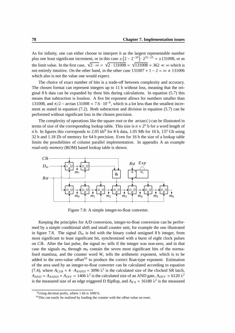
78 Chapter 7. Implementation issues
As for infinity, one can either choose to interpret it as the largest representable numberplus one least significant increment, or in this case±
(
2− 2−10)
· 231−15 = ±131008, or as
the limit value. In the first case,√
2 · ∞ =√
2 · 131008=√
131008≈ 362� ∞ which isnot entirely intuitive. On the other hand, in the other case 131007+ 1− 2 = ∞ , 131006which also is not the value one would expect.
The choice of exact number of bits is a trade-off between complexity and accuracy.The chosen format can represent integers up to 11 b without loss, meaning that the ori-ginal 8 b data can be expanded by three bits during calculations. In equation (5.7) thismeans that subtraction is lossless. A five bit exponent allows for numbers smaller than131008, andπ/2− arctan 131008≈ 7.6 · 10−6, which is a lot less than the smallest incre-ment as stated in equation (7.2). Both subtraction and division in equation (5.7) can beperformed without significant loss in the chosen precision.
The complexity of operations like the square root or the arctan(·) can be illustrated interms of size of the corresponding lookup table. This size isn× 2n b for a word length ofn b. In figures this corresponds to 2.05 kb9 for 8 b data, 1.05 Mb for 16 b, 137 Gb using32 b and 1.18 Zb of memory for 64 b precision. Even for 16 b the size of a lookup tablelimits the possibilities of column parallel implementation. In appendix A an exampleread-only memory(ROM) based lookup table is shown.
DR
Q DR
Q DR
Q DR
Q DR
Q DR
Q DR
Q
SR
Q DR
Q
&R Wc
Clk
Din
Rst
m7
m0 m1 m2 m3 m4 m5 m6
Rst Exp
Figure 7.8: A simple integer-to-float converter.
Keeping the principles for A/D conversion, integer-to-float conversion can be perfor-med by a simple conditional shift and small counter unit, forexample the one illustratedin figure 7.8. The signalDin is fed with the binary coded unsigned 8 b integer, frommost significant to least significant bit, synchronized witha burst of eight clock pulseson Clk. After the last pulse, the signalm7 tells if the integer was non-zero, and in thatcase the signalsm6 through m0 contain the seven most significant bits of the norma-lised mantissa, and the counter wordWc tells the arithmetic exponent, which is to beadded to the zero-value offset10 to produce the correct float-type exponent. Estimationof the area used by an integer-to-float converter can be calculated according to equation(7.4), whereACS R≈ 4 · ANAND= 3096λ2 is the calculated size of the clocked SR latch,AAND ≈ ANAND+ AINV = 1406λ2 is the calculated size of an AND gate,ADFF ≈ 6120λ2
is the measured size of an edge triggered D flipflop, andAFA ≈ 16180λ2 is the measured
9Using decimal prefix, where 1 kb is 1000 b.10This can easily be realized by loading the counter with the offset value on reset.
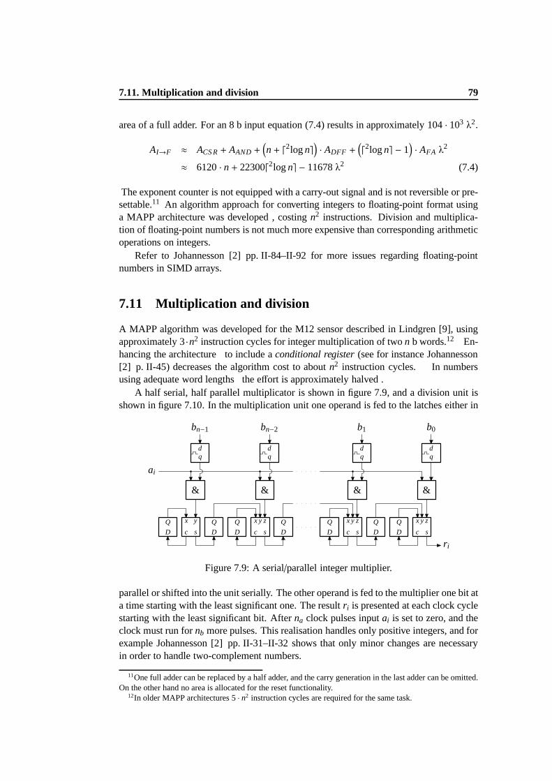
7.11. Multiplication and division 79
area of a full adder. For an 8 b input equation (7.4) results inapproximately 104· 103 λ2.
AI→F ≈ ACS R+ AAND+(
n+ d2logne)
· ADFF +(
d2logne − 1)
· AFA λ2
≈ 6120· n+ 22300d2logne − 11678λ2 (7.4)
The exponent counter is not equipped with a carry-out signaland is not reversible or pre-settable.11 An algorithm approach for converting integers to floating-point format usinga MAPP architecture was developed , costingn2 instructions. Division and multiplica-tion of floating-point numbers is not much more expensive than corresponding arithmeticoperations on integers.
Refer to Johannesson [2] pp. II-84–II-92 for more issues regarding floating-pointnumbers in SIMD arrays.
7.11 Multiplication and division
A MAPP algorithm was developed for the M12 sensor described in Lindgren [9], usingapproximately 3·n2 instruction cycles for integer multiplication of twon b words.12 En-hancing the architecture to include aconditional register(see for instance Johannesson[2] p. II-45) decreases the algorithm cost to aboutn2 instruction cycles. In numbersusing adequate word lengths the effort is approximately halved .
A half serial, half parallel multiplicator is shown in figure7.9, and a division unit isshown in figure 7.10. In the multiplication unit one operand is fed to the latches either in
D
Q
D
Q
D
Q
D
Q
D
Q
D
Q
D
Qx y
c s
x y z
c s
x y z
c s
x y z
c s
& & & &
dq
dq
dq
dq
ai
bn−1 bn−2 b1 b0
r i
Figure 7.9: A serial/parallel integer multiplier.
parallel or shifted into the unit serially. The other operand is fed to the multiplier one bit ata time starting with the least significant one. The resultr i is presented at each clock cyclestarting with the least significant bit. Afterna clock pulses inputai is set to zero, and theclock must run fornb more pulses. This realisation handles only positive integers, and forexample Johannesson [2] pp. II-31–II-32 shows that only minor changes are necessaryin order to handle two-complement numbers.
11One full adder can be replaced by a half adder, and the carry generation in the last adder can be omitted.On the other hand no area is allocated for the reset functionality.
12In older MAPP architectures 5· n2 instruction cycles are required for the same task.
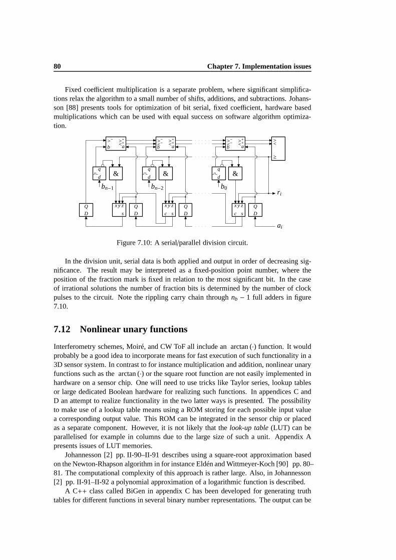
80 Chapter 7. Implementation issues
Fixed coefficient multiplication is a separate problem, where significant simplifica-tions relax the algorithm to a small number of shifts, additions, and subtractions. Johans-son [88] presents tools for optimization of bit serial, fixedcoefficient, hardware basedmultiplications which can be used with equal success on software algorithm optimiza-tion.
D
Q
bn−1
x y z
s D
Q
q
d &
>− >+<+
b a
x y z
c s D
Q
q
d &
>− >+<− <+b a
bn−2
x y z
c s D
Q
q
d &
>− >+<− <+b a
b0
><
≥
r i
ai
Figure 7.10: A serial/parallel division circuit.
In the division unit, serial data is both applied and output in order of decreasing sig-nificance. The result may be interpreted as a fixed-position point number, where theposition of the fraction mark is fixed in relation to the most significant bit. In the caseof irrational solutions the number of fraction bits is determined by the number of clockpulses to the circuit. Note the rippling carry chain throughnb − 1 full adders in figure7.10.
7.12 Nonlinear unary functions
Interferometry schemes, Moiré, and CW ToF all include an arctan(·) function. It wouldprobably be a good idea to incorporate means for fast execution of such functionality in a3D sensor system. In contrast to for instance multiplication and addition, nonlinear unaryfunctions such as the arctan(·) or the square root function are not easily implemented inhardware on a sensor chip. One will need to use tricks like Taylor series, lookup tablesor large dedicated Boolean hardware for realizing such functions. In appendices C andD an attempt to realize functionality in the two latter ways is presented. The possibilityto make use of a lookup table means using a ROM storing for eachpossible input valuea corresponding output value. This ROM can be integrated in the sensor chip or placedas a separate component. However, it is not likely that thelook-up table(LUT) can beparallelised for example in columns due to the large size of such a unit. Appendix Apresents issues of LUT memories.
Johannesson [2] pp. II-90–II-91 describes using a square-root approximation basedon the Newton-Rhapson algorithm in for instance Eldén and Wittmeyer-Koch [90] pp. 80–81. The computational complexity of this approach is ratherlarge. Also, in Johannesson[2] pp. II-91–II-92 a polynomial approximation of a logarithmic function is described.
A C++ class called BiGen in appendix C has been developed for generating truthtables for different functions in several binary number representations.The output can be

7.12. Nonlinear unary functions 81
used either in a Boolean optimization program, for example BOOL [89] as exemplifiedin appendix D, or as data in a lookup table. The condition for BiGen to work is that theunary function is described by a C function taking as input a 64 b argument in the formof an IEEE standard floating-point number as described by Hollasch [87] and returning a64 b output in the same form. This function is then directed tothe C++ class constructorin the form of a function pointerdouble (*new_procfn)(double) .


Part III
A case study
83


CHAPTER 8
Components in the sensor chip
This chapter contains proposals for the sensor chip.
8.1 A pixel
For the 3D snap case study the most suitable choice would be a combination of CWmodulation ability, like in the pixel of Kimachi and Ando [66] in subsection 7.1.4, andsynchronous shutter ability, like the pixel of Johansson [78] in 7.1.3. Looking at the twostructures raises the thought that the first is much like the second, only with two analo-gue memories1. The main difference is that the shutter transistor gate is controlled by ananalogue sine wave in the first case and by a two-valued logical signal in the second case.Adding more memory and enabling charge sharing between themprovides support for3D acquisition schemes using sequentially coded light (seesection 5.7) and backgroundadapted thresholding (section 7.8). The proposed pixel, shown in figure 8.1, has not beenevaluated in depth, but its behaviour can be reasoned by applying general electrostaticknowledge. Basically, by applying a differential sine wave on two of the signalsS hutteriandS hutterj demodulation is performed in the same way as in Kimachi and Ando [66],whereas applying binary signals to the shutter gates performs synchronous sampling ofthe image. The large quantity of components in the pixel would require TFA diodes orat least microlenses (see section 7.6) to improve fill factor. Also, since storage capaci-tors must be significantly larger than the unwanted parasitic capacitances and since noisesources should be minimized each component becomes rather large.
The readout circuitry currently used in Lindgren et alii [9]is able to perform doublesampling, meaning that the output from a pixel is the difference between two readoutsfrom the same photodiode or even from two arbitrary pixels inthe same column. Nor-mally the values are a reset value and an integrated light value from the same pixel. Thetechnique is calledcorrelated double sampling(CDS)2 if the reset value used is sampled
1Integrating or sample capacitors.2Or true CDS by some.
85

86 Chapter 8. Components in the sensor chip
Reset
Shutt
er 0
Sele
ct 0
Shutt
er 1
Sele
ct 1
Shutt
er 2
Sele
ct 2
Shutt
er 3
Sele
ct 3
PO
N
Colu
mn
bu
s
Figure 8.1: An active pixel with several analogue memories.

8.2. A suitable ALU 87
from the same image acquisition cycle as the signal3. Background light suppression canbe achieved by reading a difference between the image value and a dark value4 from thesame pixel. The subtraction can be performed exactly as the normal double samplingaction, and in the process an equivalent to normal double sampling is also achieved.5 Intime domain correlation the desired value is often the difference between positive andinverted correlation results, which is also easily achieved in the readout circuitry.
A/D conversion strategies are also inherited from Lindgren etalii [9]. The currentA/D conversion architecture gives excellent results, so there is no reason to change thisstructure. The architecture is a single slope A/D converter, which is very suitable forparallelism in one or two dimensions since much of the analogue functionality can beshared between channels. Assuming that the A/D conversion can be performed with fullspeed, one frame of 5122 pixels is converted into 8 b digital data in 4 ms, allowing fortenfull A /D conversions while maintaining the limit of 25 images per second. If a system isused where A/D conversion is performed in-pixel, perhaps multi-channelbit-serial A/Dconversion (see El Gamal et alii [76] or subsection 7.1.2) isa better alternative, requiringonly minor changes to the bit-parallel scheme.
8.2 A suitable ALU
The MAPP architecture described in detail in subsection 7.1.1 could easily be enhancedto accomodate a conditional register . Also a new structure for a PLU was developedand is strongly recommended since it provides more flexibility than older organizationswithout significant cost increase.
Apart from normal performance enhancement such as optimized acceleration networksand new faster clocking schemes, there are two strategies for improving the overall be-haviour of the ALU in terms of 3D snap. Both include communicational changes withinthe column processors consisting of splitting the ALU bus into smaller fragments, eachconnecting a subset of data processing components, memory,data inputs or outputs, andat least one other bus fragment. By connecting all fragmentsto a long bus, communi-cation is performed as previously with one global ALU bus. Otherwise each individualfragment supports one source and at least one destination, thereby enabling parallel busaccess. The performance of each bus fragment must be fast enough to compensate for thecascaded components.
Both strategies also propose trading off horizontal computational power in favour ofcolumn oriented performance. That is, the two units which can be sacrificed to makeroom for the proposed ALU are the GLU and the NLU. An NLU uses around 42054λ2
of chip area.6
The units GLU, NLU, and COUNT/GOR serve no purpose in the choice of 3D acqui-sition scheme, but they may very well be useful in general purposes such as image filtering
3As opposed to ‘any’ reset signal not directly correlated to the signal sample, for instance, the reset fromthe previous signal sample.
4Or the average of a dark and a bright value. Averaging can be performed within the proposed pixel by asimple charge sharing between two analogue memories.
5True CDS is however not performed in this operation.6A significant part of the NLU consists of vertical metal wire routing. An extra metal layer in the process
would probably allow for some area optimization.

88 Chapter 8. Components in the sensor chip
or algorithm control. To exclude a unit from a previous imagesensor chip requires carefulconsideration of the consequences.
Output register
Int-to-float convBus splitter/bridge
General registers
Mult/Div unitBus splitter/bridge
General registers
Readout & A/D conv
Figure 8.2: An ALU proposal using specialized units.
The first strategy is based on a number of specialized units such as the integer-to-float converter in figure 7.8, the multiplicator in figure 7.9,and the division circuit infigure 7.10. The advantage is highly optimized hardware, butthe cost is specialized hard-ware not being able to perform other tasks. The unit Mult/Div in figure 8.2 is combinedfrom specialized serial/parallel multiplication and division circuits. The original outputis actually a fixed-point number, and with only a small amountof additional hardwarefloating-point conversion can be made directly within the computational unit. The dedi-cated int-to-float unit can be omitted entirely (and therefore also the second bus splitter)provided that the mult/div unit is fast enough.7 The VIP processor described in Johan-nesson ([2] pp. II-31–II-32) in subsection 7.3.1 features aparallel load option for globalcoefficients to the multiplication hardware. This function can beused for various purposeswhere external data is fed to all or a subset of column processors.
The second and strongly recommended alternative shown in figure 8.3 is based on ageneralized, SIMD type programmable PLU. It combines computational power with flex-ibility at the expense of instruction word width. Hence, in order to minimize instructionword length, predefined macros instead of actual instructions might be useful. Such anenhancement would require extra hardware in the decoder area. The size of a PLU isabout 181556+ n · 3059λ2 of chip area,8 wheren is the number of accumulator registersassociated with the PLU.
7A straight-forward conversion can be performed with the second operand set to 1.8An extra metal layer in the process would probably decrease area also for the PLU.
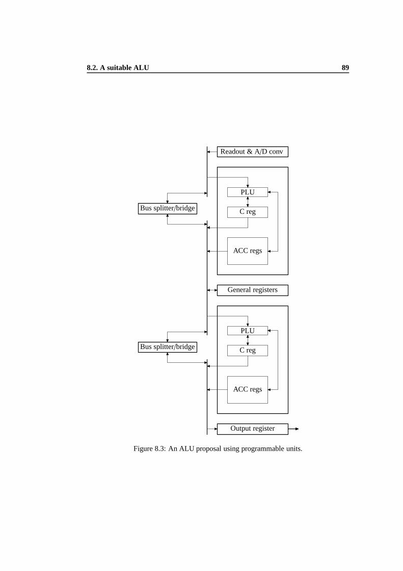
8.2. A suitable ALU 89
Output register
ACC regs
C reg
PLU
Bus splitter/bridge
General registers
ACC regs
C reg
PLU
Bus splitter/bridge
Readout & A/D conv
Figure 8.3: An ALU proposal using programmable units.


CHAPTER 9
Off-sensorchip camera components
Some components are not suitable for on-chip integration, for example, large area consu-ming memories. A solution is proposed where area consuming data path components areplaced externally to the sensor chip.
9.1 Data path look-up tables
Off-camera communicationData memory
I/O controller
Sensor LUT memory
Instr Ctrl
Data
Data
Ctrl
Ctrl
Data Ctrl Instr
Data Data
Figure 9.1: FPGA and LUT in the data path.
A LUT based implementation of the arctan(·) function described in section 7.12requires a rather large ROM in addition to a control mechanism of some sort. If thefunctionality is to be reconfigured the LUT memory should be made writeable. The mostflexible solution is to implement a rather small controller in an FPGA in the data pathdirectly outside the sensor chip data port, as illustrated in figure 9.1, and connect it to theLUT memory. Throughput demands can be taken from the numbersin section 7.4, thatis, nOUT · X × Y look-ups per second are required for one single non-linear function perpixel. Additional throughput is probably best acquired by interleaving between severalparallel hardware doublets.
91

92 Chapter 9. Off-sensorchip camera components
9.2 Off-chip controller
For simplicity the traditional SICK IVP approach for controlling program execution flowin subsection 7.9.1 is assumed, although the integrated controller in subsection 7.9.2 isfeasible. Also for off-camera communication the accepted SICK IVP approach in sub-section 7.9.3 is recommended.
9.3 Off-camera communication
To satisfy the criteria of this project, data sent from the camera should only be the pro-cessed result, meaning that a capacity of 25· 5122 · sPIXEL B/s is sufficient. Using the16 b floating-point data format proposed in section 7.10sPIXEL = 2 B, results in a totalrequirement of around 100 Mb/s, which is achieved in current SICK IVP camera systems.Refer to for instance Klaar [91] for further information on communication.

Part IV
Conclusion
93


CHAPTER 10
Conclusion
Within the frame of this project the goals were to find one or more ways to build a 3D snapsensor fulfilling the specified requirements on speed and resolution, among other things.Studying the basics of a number of known schemes for general 3D acquisition revealedthat there seems to be no way of fulfilling all the criteria with existing techniques. Ho-wever, trading off one or two requirements is enough relaxation for the remaining goalsto be fulfilled. Also, hardware support for phase calculations, noise reduction techni-ques such as suppression of background light, globally synchronous shutter techniques,and possibility of mixing detected light with a modulation signal within the image sensorpixels are details likely to improve the chances for a 3D snapsensor. Projection techni-ques are also key factors for several 3D schemes, so it is of interest for future 3D sensordesign to remain continually informed about performance limits for existing projectortechnologies.
Highly integrated near-sensor architectures like NSIP areof little use unless verticalintegration like for example TFA photosensors can be manufactured with fairly good qua-lity. On the other hand, fast image processing requires dataintensive communication thatis very hard to implement over chip boundaries but is fairly easy to achieve on-chip due tothe opportunities for parallelism. The more work that is done early in the data processingchain, for instance within each pixel, the more relaxed are the requirements on compu-tational devices further down the readout chain. Data reduction in the analogue domainallows for faster A/D conversion with lower resolution without significant precision loss.
10.1 Future work
The author’s recommendation regarding 3D snap sensors is tostart by drawing a com-plete and detailed picture of what are the important features in a future 3D imaging sy-stem. This will act as grounds for making the decision which of the demands set in thisproject are optional and which ones must absolutely be met. Perhaps even the snapshotrequirement is unnecessary; there may be easier ways to solve the underlying problemsthat proposed this demand in the first place. Hopefully therewill be room for enough re-laxations for one of the schemes listed in chapter 5 to appearas a good candidate. There
95

96 Chapter 10. Conclusion
is probably enough work for another master’s thesis projectjust to study this particularscheme and decide its limitations.
Design and implementation is a multi-front battle: choice of a suitable light source de-sign, mechanics for fixating or moving the scene, choice of optics, camera system design,and last but not least the actual image sensor hardware. Three main branches providea good first selection, since schemes making use of stereo vision and those relying oninterferometry have very different demands than other schemes regarding system design.For example, since stereo schemes make use of several imagessuch a system needs se-veral sets of optics and image sensors, and high-speed off-chip communication with aspecialized computational hardware.
Chapter 11 contains a list of tasks that were not made during this project. Applicableparts of it should also be included in the future work in orderto avoid any incorrectdecisions.

CHAPTER 11
Discussion
There are several things that should be included in this workbut have been left out due tolimited resources.
11.1 Implementability
Studying different light sources, lasers, liquid crystal masks, and available processes re-garding price, availability, and performance limits wouldgive a good idea about the costfor both development and production of a 3D snap sensor.
11.2 Architectures
Checking performance of components such as memories, DSP, and DFT computationalunits available as standard hardware components might reveal possibilities and obstaclesconcerning dedicated image sensors and off-chip computational hardware, which wouldbe valuable to the conclusions in this project.
Analogue behaviour of the proposed pixel should be examinedin detail. The ratherlarge parasitic capacitances will render pixel design difficult even with the possibility ofTFA techniques.
11.3 Optical environment
Lacking deeper knowledge of limitations in optics such as aberrations, diffraction, andsensitivity no quantitative calculations have been made concerning optical scenery. Ex-pected performance of projectors concerning for instance focus is approximated usingmeasurements and calculations in the literature. A quantitative study of available modu-lated light using for example gratings of certain types would be informative.
97

98 Chapter 11. Discussion
11.4 Literature search
Most of the literature used in this study can be found using common search tools on theInternet.1 The sources of articles and dissertations have been considered in validatingthe contents. Most literature is published at universitiesaround the world, but some in-formation is available from companies and institutions with economical interest in theproducts or methods described in the text. Also, unofficial information has come to theauthor’s knowledge concerning some of the referenced material, and has contributed tothe suggestions in this text.
11.5 Optically optimized processes
Apart from general CMOS processes, the development of processes optimized for ima-ging circuitry improves rapidly. Solutions based on such processes are not included inthis project but are of interest for the design of a 3D snapshot sensor.
11.6 Imaging components for mass markets
A large number of small image acquisition units used in for instance cellular phones areavailable today. They are inexpensive and often include complete lens systems as well asadvanced image sensors in packages significantly smaller than 1 cm3. Such small unitsare perhaps useful in for example stereo schemes.
1The one used absolutely most often for this work was in fact Google, http://www.google.com.

Appendices
99


APPENDIX A
Lookup tables
The physical size of a look-up table can be expressed in scalable terms, in the lengthunit λ , which is related to half the minimum drawable channel length for a given CMOSprocess. Consider the six by eight bit cells in an example n-type channel metal oxidesemiconductor(NMOS) inverting OR(NOR) ROM as shown in figures A.1 and A.2.
bit 3
bit 2
bit 3
bit 1
bit 2
bit 0
bit 1
bit 0
word0
word1
word2
word3
word4
word5
Figure A.1: An example NMOS NOR ROM 6×8 b cell schematic.
Readout is precharged, that is, the bit lines must be chargedto the positive supply voltagebefore any address line is activated. One individual memorybit measuressROM = 8 λ
101

102 Chapter A. Lookup tables
on each side using MOSIS rules1. A test layout in an example 0.35µm CMOS processindicates that the relative size is likely to increase somewhat in smaller processes, sincethe linear scaling model does not hold for smallerλ . In figures A.3 and A.4 a simpletwo-input NOR gate is shown. The physical size of ann-input NOR gate can be expres-sed according to equation (A.1) for NMOS widths smaller thanthe minimum contacteddiffusion as in figure A.3, and according to equation (A.2) for larger NMOS transistors.
ANOR(n) = (9 · n+ 8) ×(
3 · n · kµ + 25)
λ2, 3λ ≤ wNMOS < 5λ (A.1)
ANOR(n) = (8 · n+ 8) ×(
5 · n · kµ + 25)
λ2,wNMOS ≥ 5λ (A.2)
The factorkµ compensates for the lower mobility in PMOS channels. If the memoryis not partitioned to keepn small it might be more economical to use pairs ofinvertingAND (NAND) gates and inverters instead of NOR gates. By placing all odd word addressdecoders on one side of the ROM and all even ones on the other the problem of limitedword pitch can be reduced.mwords ofn b data requiresAROM λ
2 of ROM cells,AADR λ2
for address wires, andm NOR gates withd12 ·2 logme inputs,
AROM (m, n, sROM) = m× n · s2ROMλ
2 (A.3)
AADR(m, n, sROM) = m× 2 · d2logme · sROM× 7λ2 (A.4)
provided that the address is distributed in groups of binarypairs predecoded into groupsof four one-hot signals as shown in figure A.5. The predecoderconsists of four 2-inputNAND gates and two inverters, takingAPREDEC= 4360λ2 in total. By analogy with theROM cells described earlier, nonlinear effects in the scaling of CMOS processes causea layout in an example 0.35µm CMOS process to exceed the expected size somewhat.The total area used for the ROM lookup table depends on the number of metal layersavailable. The ROM cells and the NOR gate2 use only one layer of polysilicon and onelayer of metal. The predecoded addressing lines are drawn inparallel with the long metalwires in the ROM cells. With only one metal layer available, the address lines should berouted in metal and selected lines routed to the word decoderin polysilicon. In this casethe total area used by the ROM is a simple sum of the component areas. One extra metallayer means that the word decoders and the routed signals mayshare space as long asselected address lines can be contacted between the second metal layer and polysilicon.The long address wires are routed in the top metal layer. Presence of a third layer meansthat the total area is the larger part of routing and other components, since wires can bestacked onto logic. Long wires are routed in the third metal layer and selection is madein the second layer.
Note that the eight metal bit lines in figure A.2 work in complementary pairs. Thesensing electronics may operate at greater speed or may be sized more economically thanfor single-ended solutions. On the other hand the word length capacity is halved usingthe same area. The wires are ordered so that
1MOSIS scalable CMOS design rules, revision 7.2 according toKang and Leblebici [5], with added capa-bility of π/4 rad edges. The later improvement has little impact on the cell size but may improve productionyield.
2And of course other primitive cells like the NAND and the inverter.
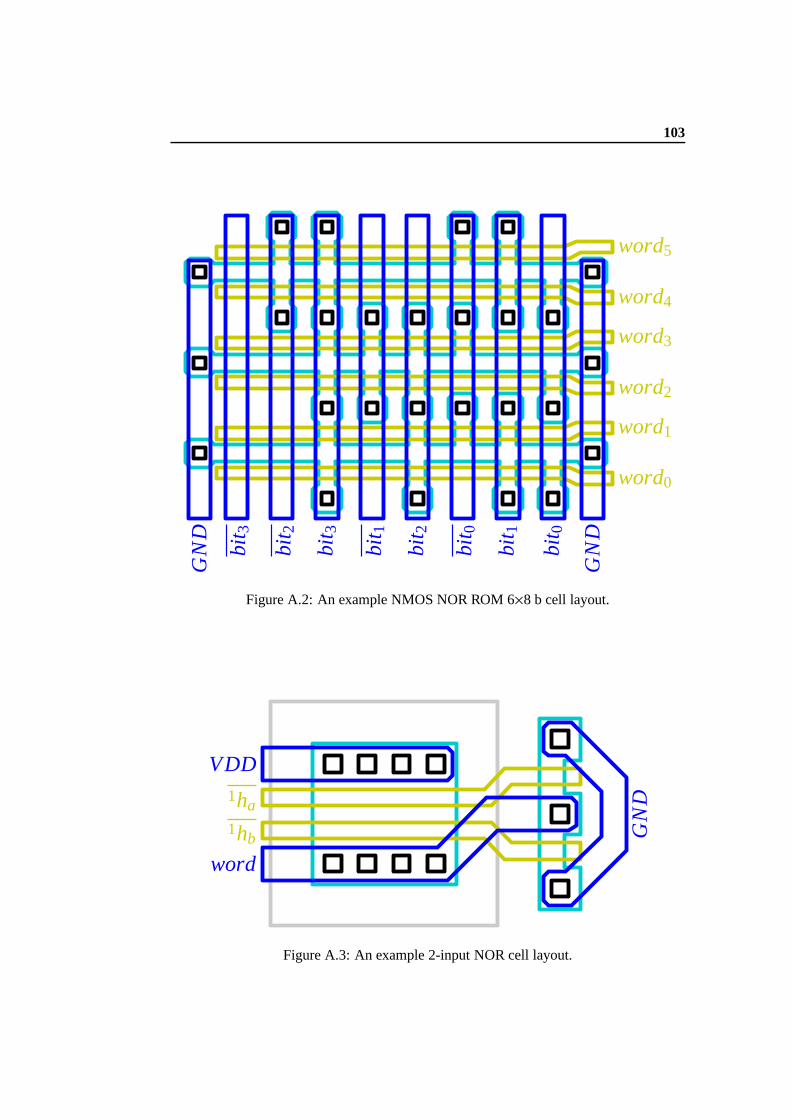
103
bit 0
bit 0
bit 1
bit 1
bit 2
bit 2
bit 3
bit 3
word0
word1
word2
word3
word4
word5
GN
D
GN
DFigure A.2: An example NMOS NOR ROM 6×8 b cell layout.
VDD
GN
D
word
1ha
1hb
Figure A.3: An example 2-input NOR cell layout.

104 Chapter A. Lookup tables
word
1ha
1hb
Figure A.4: An example 2-input NOR cell schematic.
& & & &Enable
b1b0
1h 3
1h 2
1h 1
1h 0
Figure A.5: A 2 b binary to 4 b one-hot predecoder.

105
1. no wire neighbours to its own inverse, and
2. if a wirexneighbours to the signaly, the inverse of the signalxhas no direct contactwith the inverse ofy.
The purpose is to improve differential SNR by spreading correlated noise sources. Notealso that in a differential structure all polysilicon word lines are loaded bythe same num-ber of gates. An example circuit for differential sensing is shown in figure A.6.
In+
Read
In−
Lock
Rst
Out+
Lock
Figure A.6: A sense amplifier for differential readout.


APPENDIX B
SBCGen
This appendix contains C++ source code and some results for a stripe boundary codegenerator following the criteria presented by Hall-Holt and Rusinkiewicz [26]. Input tothe program is a one-digit decimal integer between 1 and 8.1 The conditions for theresulting stripe boundary codes are enumerated below.
1. There are no constraints on the nodes themselves. Usingn bits, the number of rawnodes is 2n.
Each pair of two raw nodes is examined to determine if they form a valid rawboundary. If so, the boundary is added to the list of possibleboundaries for each ofthe two nodes.
2. A valid boundary is not static. In the example program the threshold is set to atleast three different temporal conditions so that at least two changes occurin theboundary during the sequence.
3. A valid boundary must not be invisible for more than one single frame before re-appearing.
Starting at a valid boundary, its two nodes are the first two nodes in a stripe boundarycode. The code is then grown by repetitively selecting one ofthe set of possibleboundaries associated with the last node in the code.
4. In each frame no two neighbouring boundaries can be invisible, that is, the greatestdistance between two visible boundaries at any time is one single node.
The second node of the selected boundary is appended to the code, and a newpossible boundary is selected, if possible. The code reaches its end when there areno possible boundaries left at the last node.
1The upper limit is set so that a value can be stored using one byte only. On a machine using 32 b integersthe program can easily be rewritten to accomodate 31 b if required, although the size of the output as well asthe computational work will increase rapidly.
107

108 Chapter B. SBCGen
B.1 Stripe Boundary Code results
Listed in table B.1 are some of the results from running the program SBCGen, and tableB.2 shows a short section of a stripe boundary code with 6 frames.
Bits n Good pairs Longest code Shortestcode
4 48 12 2
5 252 73 2
6 1012 531 246
7 3528 2157 1448
8 11800 5693 4088
Table B.1: Some stripe boundary code results.
Node Visible Sequences000101
010010 010111 6
111101 101111 5
101010 010111 6
010111 111101 6
100000 110111 4
010111 110111 4
101010 111101 6
000100 101110 6
110011 110111 4
001110 111101 4
010001 011111 4
001110 011111 4
110101 111011 5
011011 101110 6
Table B.2: A stripe boundary code example.
B.2 Header file NodeClass.h
// NodeClass.h: interface for the NodeClass class.
//
//////////////////////////////////////////////////////////////////////
#ifndef NODECLASS
#define NODECLASS
#define CHUNKSIZE 16
#define INTSIZE sizeof(int)
#define BYTE unsigned char
#define NULL 0
#define ERR_HEXDIG 1

B.3. Source file NodeClass.cpp 109
#define ERR_MEMALL 2
#define ERR_NONVAL 4
class NodeClass
{
public:
NodeClass(int nodevalue);
~NodeClass(void);
static int set_hexdig(int hexdigits); // Forms output string, returns error.
int add_bound(int node); // Adds a new boundary, returns error.
int boundcount(int lastnode, int lastvis, int mask);
// Returns number of boundaries.
int print_node(void); // Returns short string as an integer.
int get_next(int lastnode, int lastvis, int mask);
// Returns and deletes a node, negative indicates error.
void reset_bound(void); // Resets all boundary nodes.
protected:
private:
NodeClass(void) {};
int tmpnodecount;
int maxnodecount;
BYTE ownvalue;
BYTE* boundnodes;
};
extern NodeClass** nodes;
#endif // !defined NODECLASS
B.3 Source file NodeClass.cpp
// NodeClass.cpp: implementation of the NodeClass class.
//
//////////////////////////////////////////////////////////////////////
#include <stdio.h>
#include <string.h>
#include "NodeClass.h"
//////////////////////////////////////////////////////////////////////
// Global memory, to avoid problems with static members.
//////////////////////////////////////////////////////////////////////
static char* printstring = NULL;
//////////////////////////////////////////////////////////////////////
// Construction
//////////////////////////////////////////////////////////////////////
NodeClass::NodeClass(int nodevalue)
{
ownvalue = nodevalue;
maxnodecount = 0;
boundnodes = NULL;
}
//////////////////////////////////////////////////////////////////////
// Destruction
//////////////////////////////////////////////////////////////////////

110 Chapter B. SBCGen
NodeClass::~NodeClass()
{
if (boundnodes != NULL)
delete[] boundnodes;
if (printstring == NULL)
delete[] printstring;
}
//////////////////////////////////////////////////////////////////////
// Output formatting.
// Forms output string, returns error.
//////////////////////////////////////////////////////////////////////
int NodeClass::set_hexdig(int hexdigits)
{
if (printstring == NULL)
printstring = new char[CHUNKSIZE];
if (printstring == NULL)
{
printf("Error: Memory allocation failed.\n");
return ERR_MEMALL;
}
if (hexdigits >= INTSIZE)
{
printf("Error: %d hex digits is more than maximum %d.\n",
hexdigits, INTSIZE);
strcpy(printstring,"???");
return ERR_HEXDIG;
}
// if (strcmp(printstring,"") == 0)
// {
sprintf(printstring,"%%0%dx", hexdigits);
// }
return 0;
}
//////////////////////////////////////////////////////////////////////
// Adds a new boundary, returns error.
//////////////////////////////////////////////////////////////////////
int NodeClass::add_bound(int node)
{
BYTE* tmpnodes;
int i;
if (boundnodes == NULL) // This is the first boundary node.
boundnodes = new BYTE[CHUNKSIZE];
else if ((maxnodecount%CHUNKSIZE) == 0)
{ // Out of memory, must allocate more.
tmpnodes = new BYTE[maxnodecount+CHUNKSIZE];
for (i=0; i<maxnodecount; i++) // Copy from old to new.
tmpnodes[i] = boundnodes[i];
delete[] boundnodes; // Free old memory.
boundnodes = tmpnodes; // Move new memory.
}
if (boundnodes == NULL) // Allocation failed.
{
printf("Error: Memory allocation failed.\n");

B.3. Source file NodeClass.cpp 111
return ERR_MEMALL;
}
boundnodes[maxnodecount++] = node; // Store new boundary node.
return 0;
}
//////////////////////////////////////////////////////////////////////
// Returns number of boundaries.
//////////////////////////////////////////////////////////////////////
int NodeClass::boundcount(int lastnode, int lastvis, int mask)
{
int i;
int tmp = 0;
if (boundnodes != NULL)
{ // There exist boundaries.
for (i=0; i<tmpnodecount; i++)
{ // Loop over all remaining boundaries.
if (((lastnode^boundnodes[i]) | lastvis) == mask)
tmp++; // All boundaries visible at least every other node.
}
return tmp;
}
tmpnodecount = 0;
return 0;
}
//////////////////////////////////////////////////////////////////////
// Returns short string as an integer.
//////////////////////////////////////////////////////////////////////
int NodeClass::print_node(void)
{
char nodestring[INTSIZE];
sprintf(nodestring, printstring, (int)ownvalue);
return *(int*)nodestring;
}
//////////////////////////////////////////////////////////////////////
// Returns and deletes a node, negative error.
//////////////////////////////////////////////////////////////////////
int NodeClass::get_next(int lastnode, int lastvis, int mask)
{
int i, maxnode, tmpcnt, vis;
int maxcnt = 0;
int maxi = 0;
if (boundnodes == NULL)
{ // No boundary nodes available.
maxnodecount = 0;
return -ERR_NONVAL;
}
if (maxnodecount <= 0)
{ // No boundary nodes available.
delete[] boundnodes;
boundnodes = NULL;
return -ERR_NONVAL;
}
if (tmpnodecount <= 0)
{ // No boundary nodes available.

112 Chapter B. SBCGen
return -ERR_NONVAL;
}
for (i=0; i<tmpnodecount; i++)
{
vis = lastnode^boundnodes[i]; // Visible boundaries.
tmpcnt = nodes[boundnodes[i]]->boundcount(boundnodes[i], vis, mask);
if (tmpcnt > maxcnt)
{
maxcnt = tmpcnt;
maxi = i;
}
}
maxnode = boundnodes[maxi];
if (tmpnodecount > 1) // Move the last boundary node to current location.
{
boundnodes[maxi] = boundnodes[--tmpnodecount];
boundnodes[tmpnodecount] = maxnode;
}
else // No boundaries left in this node.
tmpnodecount = 0;
return maxnode;
}
//////////////////////////////////////////////////////////////////////
// Resets all boundary nodes.
//////////////////////////////////////////////////////////////////////
void NodeClass::reset_bound(void)
{
if (boundnodes == NULL)
{ // No boundary nodes available;
maxnodecount = 0;
}
else if (maxnodecount <= 0)
{
delete[] boundnodes;
boundnodes = NULL;
}
tmpnodecount = maxnodecount;
}
//////////////////////////////////////////////////////////////////////
B.4 Main file SBCGen.cpp
#include <ctype.h>
#include <stdio.h>
#include "NodeClass.h"
NodeClass** nodes = NULL;
void main(int argc, char* argv[], char* envp[])
{
int bits = 8; // in [1,8].
int raws; // = 1<<bits;
int i, j, k, tmp, mask, used;
int start = 0;
int bottom;
int botcnt = 0;
int top = 0;
int topcnt = 0;

B.4. Main file SBCGen.cpp 113
int lastnode, lastvis;
int newseq, prevseq, seqcnt, seqthresh;
const char* pathprefix = "\nSBC = ";
const char* pathsuffix = ";\n";
const char* hexprefix = "0x";
const char* separator = ", ";
const char* remprefix = "REM = ";
const char* remsuffix = ";\n\n";
const char* useprefix = "USE = ";
const char* usesuffix = ";\n";
const char* botprefix = "LOW = ";
const char* botseptor = "(x";
const char* botsuffix = ");\n\n";
const char* topprefix = "\nHGH = ";
const char* topseptor = "(x";
const char* topsuffix = ");\n";
if (argc > 1)
{
i = 0;
bits = 0;
while (isdigit(argv[1][i]))
bits = bits*10+(int)(argv[1][i++]-’0’);
if ((bits <= 0) || (bits > 8))
{
printf("Error: Usage %s <bits>, decimal digits only, max 8 bits.\n", argv[0]);
return;
}
}
raws = 1<<bits;
bottom = raws*(raws-1)/2+1;
mask = (1<<bits)-1;
if (bits < 3) // 3 sequences not possible.
seqthresh = bits; // Adjust dynamic condition.
else
seqthresh = 3; // At least two breaks in a boundary temporal sequence.
nodes = new NodeClass*[raws];
for (i=0; i<raws; i++)
nodes[i] = NULL;
for (i=0; i<raws; i++)
{ // Generate raw nodes.
if (nodes[i] == 0)
nodes[i] = new NodeClass(i);
for (j=i+1; j<raws; j++)
{ // Generate raw boundaries.
tmp = i^j; // Visible boundaries.
tmp |= tmp<<1;
if (((tmp&mask) == mask) || (((tmp>>1)&mask) == mask))
{ // Good boundary shows every other frame.
prevseq = 0;
seqcnt = 0;
for (k=0; k<bits; k++)
{ // Check for dynamic
newseq = (((i>>k)&1)<<1) | ((j>>k)&1); // Sequence is 0..3.
if (newseq != prevseq)
{ // A new sequence was found.
seqcnt++;
prevseq = newseq;
}
}
if (seqcnt > seqthresh)
{ // Enough dynamic.

114 Chapter B. SBCGen
nodes[i]->add_bound(j);
if (nodes[j] == 0)
nodes[j] = new NodeClass(j);
nodes[j]->add_bound(i);
}
}
}
}
if (NodeClass::set_hexdig((bits+3)/4)) // Number of hex digits.
{
for (i=0; i<raws; i++)
delete nodes[i];
delete[] nodes;
return;
}
for (i=0; i<raws; i++)
nodes[i]->reset_bound(); // Restart the node.
lastnode = 0;
lastvis = mask; // No demand on first boundary.
start = 0;
while ((start < raws) && (nodes[start]->boundcount(lastnode, lastvis, mask) <= 0))
start++; // Search for a start node.
if (start >= raws)
{
printf("Error: No good boundaries exist using %d bits.\n", bits);
}
while (start < raws)
{
printf("%s", pathprefix); // Print new path.
tmp = nodes[start]->print_node();
used = 1; // First node in the path.
printf("%s%s", hexprefix, (char*)(&tmp)); // Print first node.
lastnode = start;
i = nodes[start]->get_next(lastnode, lastvis, mask); // Find new node.
while ((i >= 0) && (i < raws) && nodes[i]->boundcount(lastnode, lastvis, mask))
{ // There exists one more node to add.
lastvis = i^lastnode; // Last visible boundaries.
tmp = nodes[i]->print_node(); // Print next node.
used++; // A new node was used.
printf("%s%s%s", separator, hexprefix, (char*)(&tmp));
lastnode = i;
i = nodes[i]->get_next(lastnode, lastvis, mask);
}
printf("%s", pathsuffix); // End the path.
printf("%s%d%s", useprefix, used, usesuffix); // Print node count.
if (used >= top)
{ // New maximal length found.
if (used == top)
topcnt++;
else
{
top = used;
topcnt = 1;
}
}
if (used <= bottom)
{ // New minimal length found.
if (used == bottom)
botcnt++;
else
{
bottom = used;

B.4. Main file SBCGen.cpp 115
botcnt = 1;
}
}
lastvis = mask; // No demand on first boundary.
tmp = 0;
for (i=0; i<raws; i++)
{
tmp += nodes[i]->boundcount(lastnode, lastvis, mask); // Count remaining boundaries.
nodes[i]->reset_bound(); // Restart the node.
}
printf("%s%d%s", remprefix, tmp, remsuffix); // Print remaining node count.
while ((++start < raws) && (nodes[start]->boundcount(lastnode, lastvis, mask) <= 0))
start++; // Search for a new start node.
}
for (i=0; i<raws; i++)
{
delete nodes[i];
}
delete[] nodes;
printf("%s%d%s%d%s",topprefix,top,topseptor,topcnt,topsuffix);
printf("%s%d%s%d%s",botprefix,bottom,botseptor,botcnt,botsuffix);
return;
}


APPENDIX C
BiGen
This appendix contains C++ source code for the truth table generator for unary functions.Provided a function that takes a double1 and returns a double (that is, the desired unaryfunction) the class BiGen generates a truth table file suitable as input to the programBOOL. Refer to Kfir [89] for details on BOOL.
C.1 Header file BiGen.h
// BiGen.h: interface for the BiGen class.
//
// BOOL Include file generator class for converting an integer less
// than or equal to 32 bits or a floating-point number less than or
// equal to 64 bits into a 64-bit double. The result is used on a
// function returning double, and the result is converted to another
// specified format. A PLA formatted include file for BOOL is produced
// containing a truth table over the input and the result.
//
// Note: The number of input bits determines the size of the output.
//
// A 16-bit input produces a little more than 65500 lines or a little
// more than 2MB data, 32 bits input produces around 275GB, while
// 64-bit input requires more than 2.36*10^21B output.
////////////////////////////////////////////////////////////////////////
#ifndef BIGEN
#define BIGEN
#include "globals.h"
////////////////////////////////////////////////////////////////////////
// BiGen Class
////////////////////////////////////////////////////////////////////////
class BiGen
{
public:
//////////////////////////////////////////////////////////////////////
// Construction
1A C style 64 b floating-point number.
117

118 Chapter C. BiGen
//////////////////////////////////////////////////////////////////////
BiGen(double (*new_procfn)(double) = NULL,
uint32 new_inman = 8,
uint32 new_inexp = 0,
bool new_inesi = false,
bool new_imasi = false,
uint32 new_outma = 8,
uint32 new_outex = 0,
bool new_outes = false,
bool new_oumas = false);
//////////////////////////////////////////////////////////////////////
// Destruction
//////////////////////////////////////////////////////////////////////
virtual ~BiGen();
//////////////////////////////////////////////////////////////////////
// BIGVER
// Returns the version number in string format.
//////////////////////////////////////////////////////////////////////
static inline const char* BIGVER() { return "2.0.0"; }
//////////////////////////////////////////////////////////////////////
// print_bool
// Outputs a BOOL include file as a truth table.
//////////////////////////////////////////////////////////////////////
bool print_bool(ostream& output);
private:
//////////////////////////////////////////////////////////////////////
// put_together
// Creates double from sign, mantissa and exponent
//////////////////////////////////////////////////////////////////////
void put_together(double& entire,
bool sign,
uint64 mantissa, uint32 mantsize,
sint32 exponent,
sint32 expzero);
//////////////////////////////////////////////////////////////////////
// take_apart
// Creates sign, mantissa and exponent from double
//////////////////////////////////////////////////////////////////////
void take_apart(double entire,
bool& sign,
uint64& mantissa, uint32 mantsize,
sint32& exponent, sint32 expzero);
//////////////////////////////////////////////////////////////////////
// Constants
//////////////////////////////////////////////////////////////////////
static inline const uint32 d_expshift() { return 52; }
// Double mantissa size == exp shift
static inline const uint32 d_expmax() { return 10; }
// Shift to highest bit in exp
static inline const uint64 d_expincr() { return ((uint64)1 << 52); }
// LSb in exp
static inline const uint32 d_expzero() { return ((uint32)1<<10)-1; }
// Exp value of 1
static inline const uint32 d_expmask() { return ((uint32)1<<11)-1; }
// Exp bit mask unshifted
static inline const uint64 d_sign() { return ((uint64)1 << 63); }
// Sign bit mask shifted
static inline const uint64 d_mantmask() { return ((uint64)1<<52)-1; }
// Mantissa mask shifted/unshifted

C.2. Source file BiGen.cpp 119
//////////////////////////////////////////////////////////////////////
// procfn
// Function used to process output.
//////////////////////////////////////////////////////////////////////
double (*procfn)(double); // Processing function
//////////////////////////////////////////////////////////////////////
// In/out number format specification
//////////////////////////////////////////////////////////////////////
uint32 inman; // Input mantissa #b
uint32 inexp; // Input exponent #b
uint32 outma; // Output mantissa #b
uint32 outex; // Output exponent #b
sint32 inesi : 1; // Input exponent sign
sint32 imasi : 1; // Input mantissa sign
sint32 outes : 1; // Output exponent sign
sint32 oumas : 1; // Output mantissa sign
};
////////////////////////////////////////////////////////////////////////
#endif // !defined BIGEN
C.2 Source file BiGen.cpp
// BiGen.cpp: implementation of the BiGen class.
//
// BOOL Include file Generator class for converting an integer less
// than or equal to 32 bits or a floating-point number less than or
// equal to 64 bits into a 64-bit double. The result is used on a
// function returning double, and the result is converted to another
// specified format. A PLA formatted include file for BOOL is produced
// containing a truth table over the input and the result.
//
// Note: The number of input bits determines the size of the output.
//
// A 16-bit input produces a little more than 65500 lines or a little
// more than 2MB data, 32 bits input produces around 275GB, while
// 64-bit input requires more than 2.36*10^21B output.
////////////////////////////////////////////////////////////////////////
#include <math.h>
#include <time.h>
#include <iostream.h>
#include "BiGen.h"
#include "globals.h"
#define CUR_INDX 0
#define MAX_INDX 1
#define ZRO_INDX 2
////////////////////////////////////////////////////////////////////////
// BiGen Class
// Construction
////////////////////////////////////////////////////////////////////////
BiGen::BiGen(double (*new_procfn)(double),
uint32 new_inman,
uint32 new_inexp,
bool new_inesi,
bool new_imasi,
uint32 new_outma,
uint32 new_outex,
bool new_outes,

120 Chapter C. BiGen
bool new_oumas)
{
procfn = new_procfn;
inesi = new_inesi ? 1 : 0;
imasi = new_imasi ? 1 : 0;
outes = new_outes ? 1 : 0;
oumas = new_oumas ? 1 : 0;
if (new_inexp == 0) // Integer result
{
inesi = 0; // No sign on a zero
if ((new_inman + (new_imasi ? 1 : 0)) > 32)
{
cerr << "Warning: Unsupported: " << dec << new_inman
<< " bit input integer.\n";
new_inman = (new_imasi ? 31 : 32);
}
}
if (new_inman <= d_expshift())
inman = new_inman;
else
{
cerr << "Warning: Unsupported: " << dec << new_inman
<< " bit input mantissa.\n";
inman = d_expshift();
}
if (new_inexp <= d_expmax())
inexp = new_inexp;
else
{
cerr << "Warning: Unsupported: " << dec << new_inexp
<< " bit input exponent.\n";
inexp = d_expmax();
}
if ((inman + inexp + inesi + imasi) >= 64)
{
cerr << "Warning: Unsupported: " << dec
<< (inman + inexp + inesi + imasi) << " bit input.\n";
while (((inman + inexp + inesi + imasi) > 32) && (inman > 1))
inman--;
while (((inman + inexp + inesi + imasi) > 32) && (inexp > 1))
inexp--;
}
if (new_outex == 0) // Integer result
{
outes = 0; // No sign on a zero
if ((new_outma + (new_oumas ? 1 : 0)) > 32)
{
cerr << "Warning: Unsupported: " << dec << new_outma
<< " bit output integer.\n";
new_outma = (new_oumas ? 31 : 32);
}
}
if (new_outma <= d_expshift())
outma = new_outma;
else
{
cerr << "Warning: Unsupported: " << dec << new_outma
<< " bit output mantissa.\n";

C.2. Source file BiGen.cpp 121
outma = d_expshift();
}
if (new_outex <= d_expmax())
outex = new_outex;
else
{
cerr << "Warning: Unsupported: " << dec << new_outex
<< " bit output exponent.\n";
outex = d_expmax();
}
}
////////////////////////////////////////////////////////////////////////
// BiGen Class
// Destruction
////////////////////////////////////////////////////////////////////////
BiGen::~BiGen()
{
}
////////////////////////////////////////////////////////////////////////
// BiGen Class
// print_bool
// Outputs a BOOL include file as a truth table.
////////////////////////////////////////////////////////////////////////
bool BiGen::print_bool(ostream& output)
{
time_t aclock;
tm* newtime;
sint32 i;
double input_d;
sint32 input_exponent[3] = // Current, max and zero
{ 0,
inesi ? ((1 << (inexp + 1)) - 1) : ((1 << inexp) - 1),
inesi ? ((1 << inexp) - 1) : 0 };
uint64 input_mantissa[2] = // Current, max
{ 0,
(1 << inman) - 1 };
bool input_sign;
double output_d = 0; // To remove warnings
sint32 output_exponent[3] = // Current, max and zero
{ 0,
outes ? ((1 << (outex + 1)) - 1) : ((1 << outex) - 1),
outes ? ((1 << outex) - 1) : 0 };
uint64 output_mantissa[2] = // Current, max
{ 0,
(1 << outma) - 1 };
bool output_sign;
//////////////////////////////////////////////////////////////////////
// Print file header
time(&aclock);
newtime = localtime(&aclock);
output << "#\tPLA file for use with BOOL and compatibles.\n";
output << "#\tGenerated " << asctime(newtime) << "#\tby BIG version "
<< BIGVER() << ".\n\n";
output << ".i\t"
<< (inman + inexp + (inesi ? 1 : 0) + (imasi ? 1 : 0))
<< endl;
output << ".o\t"
122 Chapter C. BiGen
<< (outma + outex + (outes ? 1 : 0) + (oumas ? 1 : 0))
<< endl;
output << ".ilb"; // s e...e m...m
if (imasi)
output << "\tis\n";
for (i = inexp - (inesi ? 0 : 1); i >= 0; i--)
output << "\tie" << i;
output << endl;
for (i = inman - 1; i >= 0; i--)
output << "\tim" << i;
output << endl;
output << ".ob"; // s e...e m...m
if (oumas)
output << "\tos\n";
for (i = outex - (outes ? 0 : 1); i >= 0; i--)
output << "\toe" << i;
output << endl;
for (i = outma - 1; i >= 0; i--)
output << "\tom" << i;
output << endl;
output << ".type\tfr\n\t"; // Not specified is don’t care.
//////////////////////////////////////////////////////////////////////
// Loop input
for (input_exponent[CUR_INDX] = 0;
input_exponent[CUR_INDX] <= input_exponent[MAX_INDX];
input_exponent[CUR_INDX]++)
{ // Sweep input exponent
for (input_mantissa[CUR_INDX] = 0;
input_mantissa[CUR_INDX] <= input_mantissa[MAX_INDX];
input_mantissa[CUR_INDX]++)
{ // Sweep input mantissa
input_sign = false;
do
{
if (inexp == 0) // Integer input
{
if (imasi)
input_d = (double)((sint32)input_mantissa[CUR_INDX] |
(input_sign ? (((1 << (32 - inman)) - 1)
<< inman) : 0));
else
input_d = (double)((uint32)input_mantissa[CUR_INDX]);
}
else // if (inexp != 0), Floating-point input.
put_together( input_d,
input_sign,
input_mantissa[CUR_INDX],
inman,
input_exponent[CUR_INDX],
input_exponent[ZRO_INDX]);
output_d = procfn(input_d);
if (outex == 0) // Integer result
{
if (output_d > (double)((uint32)output_mantissa[MAX_INDX]))
{ // Overflow
output_sign = false;
output_mantissa[CUR_INDX] = output_mantissa[MAX_INDX];
}
else if ((oumas == 0) && (output_d < 0))
{ // Unsigned underflow

C.2. Source file BiGen.cpp 123
output_sign = false;
output_mantissa[CUR_INDX] = 0;
}
else if (output_d <
(double)(~((sint32)output_mantissa[MAX_INDX])))
{ // Signed underflow
output_sign = true;
output_mantissa[CUR_INDX] = ~output_mantissa[MAX_INDX];
}
else
{
output_mantissa[CUR_INDX] = (sint64)output_d;
output_sign = (output_d < 0);
}
}
else
{
take_apart(output_d,
output_sign,
output_mantissa[CUR_INDX],
outma,
output_exponent[CUR_INDX],
output_exponent[ZRO_INDX]);
}
// Print inputs
if (imasi)
output << (input_sign ? ’1’ : ’0’) << ’ ’;
for (i = (inexp - (inesi ? 0 : 1)); i >= 0; i--)
output << ((input_exponent[CUR_INDX] & (1 << i)) ? ’1’ : ’0’);
output << ’ ’;
for (i = (inman - 1); i >= 0; i--)
output << ((input_mantissa[CUR_INDX] & (1 << i)) ? ’1’ : ’0’);
output << " ";
// Print outputs
if (oumas)
output << (output_sign ? ’1’ : ’0’) << ’ ’;
for (i = (outex - (outes ? 0 : 1)); i >= 0; i--)
output << ((output_exponent[CUR_INDX] & (1 << i)) ?
’1’ : ’0’);
output << ’ ’;
for (i = (outma - 1); i >= 0; i--)
output << ((output_mantissa[CUR_INDX] & (1 << i)) ?
’1’ : ’0’);
output << "\n\t";
if (imasi)
input_sign = !input_sign;
} while (input_sign == true);
} // for (input_mantissa)
} // for (input_exponent)
output << "\n.e\n";
return false;
}
////////////////////////////////////////////////////////////////////////
// BiGen Class
// put_together
// Creates double from sign, mantissa and exponent

124 Chapter C. BiGen
////////////////////////////////////////////////////////////////////////
void BiGen::put_together(double& entire,
bool sign,
uint64 mantissa,
uint32 mantsize,
sint32 exponent,
sint32 expzero)
{
if (exponent == 0)
{
if (mantissa == 0)
{
entire = 0;
return;
}
else // mantissa != 0
{
mantissa <<= d_expshift() - mantsize; // "Normal" mantissa
exponent++; // "Normalized" exp
while ((mantissa & d_expincr()) == 0)
{
mantissa <<= 1;
exponent--;
}
mantissa &= d_mantmask();
}
}
else // exponent != 0
{
mantissa <<= d_expshift() - mantsize; // "Normal" mantissa
}
entire = (1 +
((double)((sint64)mantissa)*
pow((double)2,
(double)(-(sint32)d_expshift()))))*
pow((double)2,
(double)(exponent - expzero));
if (sign)
entire = -entire;
return;
}
////////////////////////////////////////////////////////////////////////
// BiGen Class
// take_apart
// Creates sign, mantissa and exponent from double
////////////////////////////////////////////////////////////////////////
void BiGen::take_apart(double entire,
bool& sign,
uint64& mantissa,
uint32 mantsize,
sint32& exponent,
sint32 expzero)
{
exponent = (sint32)((*((uint64*)(&entire))) >>
d_expshift()) & d_expmask();
if (exponent == 0)
{
if (entire == 0)
{
sign = false;
mantissa = 0;

C.2. Source file BiGen.cpp 125
exponent = 0;
return;
}
else // entire != 0
{
exponent = exponent - d_expzero() + 1; // Real exponent!
mantissa = *((uint64*)(&entire)) & d_mantmask();
while ((mantissa & d_expincr()) == 0) // "Normalize" exponent
{
mantissa <<= 1;
exponent--;
}
mantissa &= d_mantmask();
}
}
else // exponent != 0
{
exponent = exponent - d_expzero(); // Real exponent!
mantissa = *((uint64*)(&entire)) & d_mantmask();
}
// True mantissa, real exponent...
if (exponent < 1 - expzero)
{ // "Real" exp too small, resulting exp = 0
mantissa |= d_expincr();
while (exponent < -expzero) // "Normalize" exponent
{
mantissa >>= 1;
exponent++;
}
mantissa >>= d_expshift() - mantsize;
}
else // if (exponent >= 1 - expzero)
{
exponent += expzero;
if (exponent > ((expzero << 1) + 1))
{ // Overflow!
if (entire < 0)
sign = true;
else
sign = false;
mantissa = ((uint64)1 << mantsize) - 1;
exponent = (expzero << 1) + 1;
return;
}
else // if (exponent <= (expzero << 1) + 1)
{
if (entire < 0)
sign = true;
else
sign = false;
mantissa >>= d_expshift() - mantsize;
}
}
return;
}
////////////////////////////////////////////////////////////////////////

126 Chapter C. BiGen
C.3 Main file BigMain.cpp
#include <math.h>
#include <fstream.h> // ofstream
#include <iostream.h> // cout
#include "BiGen.h" // BiGen
#include "globals.h" // NULL
////////////////////////////////////////////////////////////////////////
// normatan
// Normalised arctan
////////////////////////////////////////////////////////////////////////
double normatan(double arg)
{
return atan(arg)*2/PI;
}
////////////////////////////////////////////////////////////////////////
// signedsqrt
// Square roots the absval, keeps the sign
////////////////////////////////////////////////////////////////////////
double signedsqrt(double arg)
{
if (arg < 0)
return -sqrt(-arg);
else
return sqrt(arg);
}
////////////////////////////////////////////////////////////////////////
// main
// Runs the generator.
////////////////////////////////////////////////////////////////////////
void main(int argc, char *argv[], char *envp[])
{
int i;
BiGen* the_generator = NULL;
ofstream the_output;
const char* filenames[] =
{ "arctan_f16.inc", "n_atan_f16.inc", "s_sqrt_f16.inc" };
const int loops = sizeof(filenames)/sizeof(filenames[i]);
double (*procfns[loops])(double) =
{ atan, normatan, signedsqrt };
const uint32 inman[loops] =
{ 10, 10, 10 };
const bool imasi[loops] =
{ true, true, true };
const uint32 inexp[loops] =
{ 4, 4, 4 };
const bool inesi[loops] =
{ true, true, true };
const uint32 outma[loops] =
{ 10, 10, 10 };
const bool oumas[loops] =
{ true, true, true };
const uint32 outex[loops] =
{ 4, 4, 4 };
const bool outes[loops] =
{ true, true, true };
for (i=0; i<loops; i++)
{

C.4. Global definitions file globals.h 127
cout << "Generating " << filenames[i] << " file.\n";
cout.flush();
the_output.open(filenames[i], // Open in current directory
ios::out | ios::trunc, // Open for output/overwrite
filebuf::sh_read);
// Share the file for reading but not for writing.
the_generator = new BiGen(procfns[i],
inman[i], inexp[i], inesi[i], imasi[i],
outma[i], outex[i], outes[i], oumas[i]);
if (the_generator != NULL)
{
if (the_output.is_open())
{
the_generator->print_bool(the_output);
the_output.close();
}
else
cerr << "Error: File " << filenames[i]
<< " is not open for output.\n";
delete the_generator;
}
else
cerr << "Error: File " << filenames[i]
<< " generator construction failed.\n";
}
return;
}
////////////////////////////////////////////////////////////////////////
C.4 Global definitions file globals.h
#define MINSTRING 16
#ifndef NULL
#define NULL 0
#endif
#if _INTEGRAL_MAX_BITS >= 64
#ifndef sint64
typedef signed _int64 sint64;
#endif
#ifndef uint64
typedef unsigned _int64 uint64;
#endif
#endif
#ifdef _WIN32
#ifndef sint32
typedef signed long int sint32;
#endif
#ifndef sint16
typedef signed short int sint16;
#endif
#ifndef uint32
typedef unsigned long int uint32;
#endif
#ifndef uint16
typedef unsigned short int uint16;
#endif
#else

128 Chapter C. BiGen
#ifndef sint16
typedef signed int sint16;
#endif
#ifndef uint16
typedef unsigned int uint16;
#endif
#endif

APPENDIX D
BOOL optimization files
This appendix contains BOOL script code for generating minimal two-level boolean ex-pressions for unary function truth tables generated by BiGen. The result can be furtheroptimized regarding area if efforts are made to identify optimal gate sharing. This has notbeen done during this project. Refer to Kfir [89] for details on BOOL.
inp is, ie[5], im[10];
bool os, oe[5], om[10];
group ingr = [is, ie, im];
group ougr = [os, oe, om];
integer i, minstatus;
string inf, ref,
inpfn1, inpfn2, inpfn3, inpfn4, inpfn5, inpfn6;
inpfn1 = "n_atan_f16.";
inpfn2 = "arctan_f16.";
inpfn3 = "s_sqrt_f16.";
inpfn4 = "un_atn_f16.";
inpfn5 = "u_atan_f16.";
inpfn6 = "u_sqrt_f16.";
for (i = 1, 6)
{
if (i == 1)
{
inf = inpfn1;
}
else if (i == 2)
{
inf = inpfn2;
}
else if (i == 3)
{
inf = inpfn3;
}
else if (i == 4)
{
inf = inpfn4;
}
129

130 Chapter D. BOOL optimization files
else if (i == 5)
{
inf = inpfn5;
}
else
{
inf = inpfn6;
}
ref = inf;
strcat(ref,"app");
strcat(inf,"pla");
open_outfile(1, ref);
printf(1, "\n/* Minimization results from ’BOpt.b’, realizing\n");
printf(1, " square roots and an arctangens functions for 16b\n");
printf(1, " signed floating-point numbers: */\n\n");
printf(1, "\n/* Opening PLA input file ’%s’ as file number %d.\n",
inf, i);
open_inpfile(i, inf);
if (readpla(i, ingr, ougr) == 16)
{
minstatus = pminimize(25, 2, ougr);
/* 63 is max, but will make most computers choke.
25 is probably good enough. */
if (minstatus == 1)
{
printf(1, "/* Optimal result from minimization #%d, */\n", i);
print(ougr);
printf(1, "/* Optimal result from minimization #%d. */\n\n", i);
}
else
{
printf(1, "/* Warning: non-minimal result #%d, */\n", i);
print(ougr);
printf(1, "/* Warning: non-minimal result #%d. */\n\n", i);
}
}
else
printf(1, "/* Error: readpla #%d failed. */\n\n", i);
open_outfile(1, "");
}
end;

131


References
[1] Justen, D.Untersuchung eines neuartigen 2D-gestützten3D-PMD-Bildverarbeitungssystems.Siegen : Universität-GH Siegen, 2001.http://www.zess.uni-siegen.de/diss/2001/justen/justen.pdf(accessed October 17th, 2002)
[2] Johannesson, M.SIMD Architectures for Range and Radar Imaging.Linköping : Linköping University, dept. of Electrical Engineering, 1995.ISBN 91-7871-609-8.
[3] Bradshaw, G.Non-Contact Surface Geometry Measurement Techniques.Dublin : Trinity College, Image Synthesis Group, 1999.http://www.cs.tcd.ie/publications/tech-reports/reports.99/TCD-CS-1999-46.pdf(accessed September 23rd, 2003)
[4] Stallings, W.Computer Organization& Architecture,6th edition.Upper Saddle River : Pearson Education, Inc., 2003.ISBN 0-13-035119-9.
[5] Kang, S.-M., Leblebici, Y.CMOS Digital Integrated Circuits: Analysis and Design,2nd edition.Singapore : McGraw-Hill Book Co. 1999.ISBN 0-07-116427-8.
[6] Åström, A.Smart Image Sensors.Linköping : Linköping University, dept. of Electrical Engineering, 1993.
[7] Gabor, D.Laser Speckle and Its Elimination.Journal of Research and Development, vol. 14, no. 5 pp. 509–514,September 1970.http://www.research.ibm.com/journal/rd/145/ibmrd1405G.pdf
133

134 REFERENCES
[8] Johansson, R., et alii.A Multi-Resolution 100 GOPS 4 Gpixels/s ProgrammableCMOS Image Sensor for Machine Vision.Linköping : IVP Integrated Vision Products AB, 2003.Presented at the IEEE workshop on CCD & AIS, Elmau, Germany, May 15th,
2003.http://www.ek.isy.liu.se/∼leifl/m12ccdais.pdf(accessed September 23rd, 2003)
[9] Lindgren, L., et alii.A Multi-Resolution 100 GOPS 4 Gpixels/s ProgrammableSmart Vision Sensor for Multi-Sense Imaging.Submitted to IEEE Journal of Solid-State Circuits May 5th, 2004.
[10] IVP AB. The fastest 3D available!http://www.ivp.se/html/products_ranger_m50.html(accessed March 23rd, 2004)
[11] SICK IVP AB. IVP Ranger M50/M40 – Product information.http://www.sickivp.se/documentation/ps/IVP Ranger M50-Information 2.0.pdf(accessed November 8th, 2004)
[12] SICK IVP AB. MultiScan on Ranger C – Several Feature Images from onecamera!http://www.sickivp.se/documentation/multiscan/Ranger_c_multiscan.pdf(accessed November 8th, 2004)
[13] Rantzer, A.Photo diodes for machine vision, Device characteristics and a-Si:Hdeposition and analysis.Linköping : Linköping University, dept. of Electrical Engineering, 2003.ISBN 91-7373-602-3.
[14] Lulé, T., Schneider, B., Böhm, M.Design and Fabrication of aHigh-Dynamic-Range Image Sensor in TFA Technology.IEEE Journal of Solid-State Circuits, vol. 34, no. 5 pp. 704–711, May 1999.http://www.imt.fb12.uni-siegen.de/he/forschung/papers/ieee_ssc99_high_dynamic_range_sensor.pdf(accessed March 23rd, 2004)
[15] Horn, B. K. P.Robot Vision.Cambridge : MIT Press, 1986. ISBN 0-262-08159-8.
[16] Paillet, F., Mercier, D., Bernard, T. M.Making the most of 15kλ2 silicon area for a digital retina PE.Arcueil : CTA/GIP, Perception for Robotics Dept., May 1998. In SPIEProceedings of Advanced Focal Plane Arrays and Electronic Cameras, vol. 3410,Zürich, Switzerland.

REFERENCES 135
[17] Kleinfelder, S., et alii.A 10 000 frames/s 0.18µm CMOS Digital Pixel Sensor with Pixel-Level Memory.Stanford : Stanford University, 2001.Presented at the International Solid State Circuits Conference, February 5th, 2001.http://www-isl.stanford.edu/∼abbas/group/papers_and_pub/isscc2001.pdf(accessed March 23rd, 2004)
[18] Wong, H.-S.Technology and Device Scaling Considerations for CMOS imagers.In IEEE Transactions on Electron Devices, Vol. 43, No. 12, pp. 2131–2142.http://ieeexplore.ieee.org/xpl/tocresult.jsp?isNumber=11893&puNumber=16(accessed June 8th, 2004)
[19] Luan, X.Experimental Investigation of Photonic Mixer Device and Developmentof TOF 3D Ranging Systems Based on PMD Technology.Siegen : Universität-GH Siegen, 2002.http://www.ub.uni-siegen.de/pub/diss/fb12/2002/luan/luan.pdf(accessed March 23rd, 2004)
[20] Schwarte, R., et alii.Schnelle und einfache optische Formerfassung mit einemneuartigen Korrelations-Photodetektor-Array.Siegen : Universität-GH Siegen, 1997.Lecture from the DGZfP-GMA trade conference in Langen April28th/29th 1997.
[21] Wolf, H. Absolute Moirémeßtechnik zur Formerfassung nicht notwendigerweisestetiger Oberflächen.Frickenhausen : ABW GmbH, 1998.http://www.fh-nuertingen.de/∼ag3d/lit /wolf_98.pdf(accessed October 11th, 2002)
[22] Wolf, K. Schnelle absolute 3D-Messung.Frickenhausen : ABW GmbH, 2002.http://www.fh-nuertingen.de/∼ag3d/lit /wolk 02.zip(accessed October 17th, 2002)
[23] Trobina, M.Error Model of a Coded-Light Range Sensor.Zürich : ETH-Zentrum, 1995.http://w3.impa.br/∼pcezar/3dp/original/trobina.pdf(accessed October 8th, 2002)
[24] Schwarte, R.Überblick und Vergleich aktueller Verfahren der optischenFormerfassung.Siegen : Universität-GH Siegen, 1997.Introduction lecture to the DGZfP-GMA trade conference, Langen, April28th/29th 1997.
[25] Pedrotti, F. L., S. J., Pedrotti, L. S.Introduction to optics,2nd edition.Upper Saddle River : Prentice-Hall, 1996.ISBN 0-13-016973-0.

136 REFERENCES
[26] Hall-Holt, O., Rusinkiewicz, S.Stripe Boundary Codes for Real-TimeStructured-Light Range Scanning of Moving Objects.Stanford : Stanford University, Stanford Computer Graphics Lab, 2001.In IEEE 8th International Conference on Computer Vision, 2001, vol. IIpp. 359–366.http://www.cs.princeton.edu/∼smr/papers/realtimerange/realtimerange.pdfhttp://w3.impa.br/∼pcezar/3dp/original/realtimerange.pdf(accessed March 23rd, 2004)
[27] Faubert, J.Motion parallax, stereoscopy, and the perception of depth:Practicaland theoretical issues.Montreal : Université de Montréal, 2001.http://mapageweb.umontreal.ca/faubert/jocelyn/papers/FaubertSPIE.pdf(accessed October 8th, 2002)
[28] Petersson, O.NSIP-kamera, Tillämpningar och algoritmer.Linköping : Linköping University, dept. of Electrical Engineering, 2002.Master’s thesis, reg. LiTH-ISY-EX-3073.
[29] Notni, G., et alii. Anwendungen der Weißlichtinterferometrie.Jena : Fraunhofer Institut für Angewandte Optik und Feinmechanik, 1997.http://www.fh-nuertingen.de/∼ag3d/lit /notni_97.zip(accessed October 8th, 2002)
[30] Chapman, B.Basic Principles of SAR Interferometry.NASA Jet Propulsion Laboratory (1995).http://southport.jpl.nasa.gov/scienceapps/dixon/report2.html(accessed October 9th, 2002)
[31] NASA Jet Propulsion Laboratory (2002).Quick facts.http://planetquest.jpl.nasa.gov/SIM/sim_facts.html(accessed October 11th, 2002)
[32] Heinol, H. G.Untersuchung und Entwicklung von modulationslaufzeitbasierten3D-Sichtsystemen.Siegen : Universität-GH Siegen, 2001.http://www.zess.uni-siegen.de/diss/2001/heinol/heinol.pdf(accessed October 21st, 2002)
[33] Choi, Y.-B., Kim, S.-W.Phase-shifting Grating Projection Moiré topography.Yusong-gu : Korea Advanced Institute of Science and Technology, dept. ofMechanical Engineering, 1998.http://pem.kaist.ac.kr/∼cliff/paper/oe98.pdf(accessed October 11th, 2002)
[34] Wiora, G.High Resolution Measurement of Phase-Shift Amplitude and numericObject Phase Calculation.Ulm : DaimlerChrysler AG, Research and Technology, August 2000.In Proceedings of Vision Geometry IX, vol. 4117 pp. 289–299,Washington,USA.

REFERENCES 137
[35] Fujita, T., Idesawa, M.New Types of Position Sensitive Device for Accurate Sensing.Chofu City : University of Electro-Communications, Graduate School ofInformation Systems, 1999.http://www.hi.is.uec.ac.jp/∼fujita/research/PSD/iciis99.pdf(accessed November 1st, 2002)
[36] IVP AB. Laser Triangulation.http://www.ivp.se/documentation/technology/LaserTriangulation.pdf(accessed October 11th, 2002)
[37] Davis, J., Ramamoorthi, R., Rusinkiewicz, S.Spacetime Stereo: A Unifying Framework for Depth from Triangulation.In IEEE Conference on Computer Vision and Pattern Recognition, June 2003,Vol. 2 pp. 359–366
[38] Curless, B., Levoy, M.Better Optical Triangulation through Spacetime Analysis.Stanford : Stanford University, Computer Science Department, ComputerSystems Laboratory, 1995.http://graphics.stanford.edu/papers/spacetime/spacetime_full.pdfhttp://www-2.cs.cmu.edu/∼seitz/course/SIGG99/papers/curl95.pdf(accessed April 3rd, 2003)
[39] NanoFocus inc., 2002.3D confocal microscopy.http://www.nanofocus-inc.com/html/3dmicro.html(accessed October 11th, 2002)
[40] Cat, H. H., et alii.SIMPil: An OE Integrated SIMD Architecture for Focal PlaneProcessing Applications.Atlanta : Georgia Institute of Technology, School of Electrical and ComputerEngineering, Packaging Research Center, 1996.http://www.ee.gatech.edu/research/pica/papers/mppoi96.ps(accessed December 2nd, 2002)
[41] Liu, Y.-F. A Unified Approach to Image Focus and Defocus Analysis.Stony Brook : State University of New York, 1998.http://www.ee.sunysb.edu/∼cvl/Publications/YFLiu_Thesis1998.pdf(accessed October 8th, 2002)
[42] Subbarao, M.On the Depth Information in the Point Spread Function of aDefocused Optical System.Stony Brook : State University of New York, 1999.http://www.ee.sunysb.edu/∼cvl/Publications/MSubbarao_TR1990.ps(accessed October 23rd, 2002)
[43] Subbarao, M., Tyan, J.-K.Selecting the Optimal Focus Measure for Autofocusing and Depth-from-Focus.Stony Brook : State University of New York, 1998.http://www.ee.sunysb.edu/∼cvl/Publications/JKTyan_PAMI1998.pdf(accessed October 23rd, 2002)

138 REFERENCES
[44] NanoFocus inc., 2002.Autofocus Measurement.http://www.nanofocus-inc.com/html/autofocus.html(accessed October 11th, 2002)
[45] Royal Philips Electronics.Philips’ fluid lenses bring things into focus.Press release, March 3rd, 2004.http://www.research.philips.com/InformationCenter/Global/FNewPressRelease.asp?lArticleId=2904&lNodeId=13(accessed May 5th, 2004)
[46] Gökstorp, M.Depth Computation in Robot Vision.Linköping : Linköping University, dept. of Electrical Engineering, 1995.
[47] Favaro, P., 2002.Depth from focus/defocus.http://ee.wustl.edu/∼fava/dfd/dfdtutorial.html(accessed October 11th, 2002)
[48] Nayar, S. K., Watanabe, M., Noguchi, M.Real-Time Focus Range Sensor.New York : Columbia University, dept. of Computer Science, November, 1994.In Proceedings of International Conference on Computer Vision, pp. 995–1001,June 1995, andin IEEE Transactions on Pattern Analysis and Machine Intelligence,Vol. 18, No. 12, pp. 1186–1198.ftp://ftp.cs.columbia.edu/pub/CAVE/papers/nayar/nayar-nabe-noguchi-sensor_pami-96.pshttp://www1.cs.columbia.edu/CAVE/publinks/nayar_pami_1996.pdf(accessed March 23rd, 2004)
[49] Liu, H., et alii.Moiré Interferometry for Microelectronics Packaging Interface FatigueReliability.Buffalo : University at Buffalo, Electronic Packaging Laboratory, andBoise : Micron Technology Inc., Quality and Reliability Assurance.From the 2002 GaAsMANTECH Conference.http://www.gaasmantech.org/2002/PDF/08f.pdf(accessed February 4th, 2002)
[50] Hochschule Mittweida, Mittweida University of Applied Sciences.Moirétechnik.http://www.htwm.de/lmt/Vorlesungen/PDF/Moire.pdf(accessed January 30th, 2003)
[51] Wang, Y., Hassell, P.Measurement of Thermally Induced Warpage of BGAPackages/Substrates Using Phase-Stepping Shadow Moiré.http://www.akrometrix.com/pdf/Tech_Papers/BGA%20Warpage%20Using%20Ph-ase%20Stepping.pdf(accessed October 3rd, 2002)
[52] Lam, Y. L. A., University of Birmingham.Moiré Fringe.http://www.geocities.com/bumbies/3d/moire.html(accessed October 16th, 2002)

REFERENCES 139
[53] PPT Vision. http://www.pptvision.com/smi.shtml(accessed November 1st, 2002)
[54] PPT VISION Announces Sale of 3D - SMI Technology AssetMinneapolis : September 2004. In Machine Vision Online usrdt2004101.http://www.machinevisiononline.org/public/articles/archivedetails.cfm?id=2184(accessed December 2nd, 2004)
[55] Albrecht, P., Michaelis, B.3D-Koordinaten durch Korrelation vonGrauwertfolgen.Magdeburg : Otto-von-Guericke-Universität Magdeburg, Institut fürProzessmeßtechnik und Elektronik, 1997.http://www.fh-nuertingen.de/∼ag3d/lit /albr_97.zip(accessed November 6th, 2002)
[56] Zhang, L., Curless, B., Seitz, S. M.Rapid Shape Acquisition Using ColorStructured Light and Multi-pass Dynamic Programming.Seattle : University of Washington, dept. of Computer Science and Engineering.In Proceedings of 1st International Symposium on 3D Data Processing,Visualization, and Transmission, Padova, Italy, June 19th/20th/21st/, 2002,pp. 24–36.grail.cs.washington.edu/projects/moscan/paper.pdf(accessed September 23rd, 2003)
[57] Ni, Y., Guan, J.A 256× 256Pixel Smart CMOS Image Sensor for Line-BasedStereo Vision Applications.In IEEE Journal of Solid-State Circuits, vol. 35, no. 7 pp. 1055–1061, July 2000.
[58] Angeli, G.The technology.http://www.netspace.net.au/∼gangeli/thetechn.html(accessed October 11th, 2002)
[59] Carlotto, M. J., 1996.Shape From Shading.http://www.newfrontiersinscience.com/martianenigmas/Articles/SFS/sfs.html(accessed October 11th, 2002)
[60] Cohen, D., Vexcel Corp.Shape From Shading Improves DEM Precision.http://www.vexcel.com/radar/shapefrshade.htm(accessed October 11th, 2002)
[61] Rice University, 2002.Holographic Interferometry.http://www.ruf.rice.edu/∼dodds/Files332/holography.pdf(accessed October 11th, 2002)
[62] McIntyre, T.Holographic Interferometry.http://www.physics.uq.edu.au/lp/lasdiag/hi.html(accessed October 11th, 2002)

140 REFERENCES
[63] Bishop, A., McIntyre, T., Rubinsztein-Dunlop, H., 1999.Near-Resonant Holographic Interferometry.http://www.physics.uq.edu.au/lp/lasdiag/hinrhi.html(accessed October 11th, 2002)
[64] Trautner, J., et alii, 2000.Mehrwellenlängen-Interferometrie zur absolutenAbstandsmessung und 3D-Bildgebung.http://kerr.physik.uni-erlangen.de/Veroeffentlichungen/InMik /jtkwgl_mehrwellen-laengen_TM_67_406.pdf(accessed October 11th, 2002)
[65] Schwarte, R., et alii.A new electrooptical mixing and correlating sensor:Facilities and Applications of the Photonic Mixer Device (PMD).Siegen : Universität-GH Siegen.Presentation from LASER ’97 in München, June 16th/17th/18th, 1997.
[66] Kimachi, A., Ando, S.Time-Domain Correlation Image Sensor: CMOS Designand Integration of Demodulator Pixels.Tokyo : University of Tokyo, Graduate School of Engineering, 2000.In Proceedings of SPIE vol. 3950, 2000.
[67] Ebersole, J. F., Wyant, J. C.Collimated Light Acoustooptic Lateral Shearing Interferometer.Lexington : Itek Corporation, Optical Systems Division, 1973.In Applied Optics, vol. 13, no. 5, 1974, pp. 1004–1005.http://www.opt-sci.arizona.edu/jcwyant/pdf/Published_Papers/Phase_Shifting/AO-%20Shearing%20Interferometer.pdfhttp://www.optics.arizona.edu/jcwyant/pdf/Published_Papers/Phase_Shifting/AO-%20Shearing%20Interferometer.pdf(accessed October 11th, 2002)
[68] Wyant, J. C.Testing Aspherics Using Two-Wavelength Holography.Lexington : Itek Corporation, Optics Laboratory, 1971.In Applied Optics vol. 10, no. 9, 1971 pp. 2113–2118.http://www.optics.arizona.edu/jcwyant/pdf/Published_Papers/Two-Wavelength/Two%20Wavelength%20Holography.pdf(accessed September 24th, 2003)
[69] Creath, K., Cheng, Y.-Y., Wyant, J. C.Contouring aspheric surfaces using two-wavelength phase-shiftinginterferometry.Tucson : University of Arizona, Optical Sciences Center, 1985.http://www.opt-sci.arizona.edu/jcwyant/pdf/Published_Papers/Two-Wavelength/-Two%20Wavelength%20Aspheric%20Testing.pdf(accessed October 31st, 2002)
REFERENCES 141
[70] Steinbichler Optotechnik GmbH.Pulsed Electronic Speckle Pattern Interferometer PulsESPI.http://www.syncretek.com/images/Product%20Literature/Steinbichler/PulsESPI_-SystemDescription.pdf(accessed October 14th, 2002)
[71] Lamprecht, J., Kranz, J., Schwider, J., 1997.Fiber Optic Phase Stepping Digital Speckle-Interferometer.http://www.optik.uni-erlangen.de/move/profile/jahresbericht-1997/Jl/(accessed October 24th, 2002)
[72] Jeremias, R., et alii.A CMOS Photosensor Array for 3D Imaging Using Pulsed Laser.Duisburg : Fraunhofer Institute of Microelectronic Circuits and Systems, 2001.In Proceedings of IEEE International Solid-State CircuitsConference,6th February 2001, pp. 252–253, 452.
[73] Iddan, G. J., Yahav, G.3D Imaging in the studio (and elsewhere. . . )http://www.3dvsystems.com/technology/Gabi_and_Giora_Article.PDF(accessed October 14th, 2002)
[74] IVP AB. Smart Vision Sensor.http://www.ivp.se/documentation/technology/TheSmartVisionSensor010518.pdf(accessed October 11th, 2002)
[75] Forchheimer, R., Åström, A.Near-Sensor Image Processing: A New Paradigm.In IEEE Transactions on Image Processing, Vol. 3, No. 6, pp. 736–746,November 1994.http://ieeexplore.ieee.org/xpl/tocresult.jsp?isNumber=7901&puNumber=83(accessed June 8th, 2004)
[76] El Gamal, A., Yang, D., Fowler, B.Pixel Level Processing – Why, What, andHow?Stanford : Stanford University, Information Systems Laboratory.
[77] Melander, J., et alii.P12 – A Passive Photodiode Pixel with Memory.Linköping : IVP Integrated Vision Products AB, 1999.Presented at the IEEE workshop on CCD & AIS.
[78] Johansson, R.Implementation of an Active Pixel Sensor with Shutter and AnalogSumming in a 0.35µm Process.Linköping : Linköping University, dept. of Electrical Engineering, 2003.Master’s thesis, reg. LITH-ISY-EX-3473-2003.http://www.ep.liu.se/exjobb/isy/2003/3473/exjobb.pdf(accessed September 23rd, 2003)
142 REFERENCES
[79] Gentile, A., et alii.Real-Time Image Processing on a Focal Plane SIMD Array.In Proceedings of IPPS 7th International Workshop on Parallel and DistributedReal-Time Systems, San Juan, Puerto Rico, April 12th–16th, 1999, pp. 400–405.http://ipdps.eece.unm.edu/1999/wpdrts/gentile.pdf(accessed March 23rd, 2004)
[80] Benthien, S., et alii.Vertically Integrated Sensors for Advanced Imaging Applications.Presented at the 25th European Solid-State Circuits Conference, Duisburg,September 21st–23rd, 1999, andin IEEE Journal of Solid-State Circuits, vol. 35, no. 7 pp. 939–945, July 2000.http://www.imt.fb12.uni-siegen.de/he/forschung/papers/esscirc99_vertically_inte-grated.pdfhttp://www.imt.fb12.uni-siegen.de/he/forschung/papers/ieee_ssc2000_vertically_-integrated.pdfhttp://ieeexplore.ieee.org/iel5/4/18446/00848201.pdf?isNumber=18446&ar-number=848201&prod=JNL&arSt=939&ared=945&arAuthor=Benthien-%2C+S.%3B+Lule%2C+T.%3B+Schneider%2C+B.%3B+Wagner%2C+-M.%3B+Verhoeven%2C+M.%3B+Bohm%2C+M.(accessed March 23rd, 2004)
[81] Lulé, T., et alii.100 000-pixel, 120-dB imager in TFA technology.In IEEE Journal of Solid-State Circuits, vol. 35, no. 5, pp. 732–739, May 2000.http://www.imt.fb12.uni-siegen.de/he/forschung/papers/ieee_ssc2000_100-000_pixel.pdf(accessed March 23rd, 2004)
[82] National Semiconductor.National Semiconductor Introduces World’s First LVDSSerDes Chipset for Very High Temperature Analog Interface Applications.Press release, January 31st, 2005.http://www.national.com/news/item/0,1735,1007,00.html(accessed April 3rd, 2005)
[83] Nesbitt, R. S., et alii.Holographic recording using a digital micromirror device.Cambridge : Massachusetts Institute of Technology, Spatial Imaging Group,Media Laboratory. In SPIE Proceedings of Practical Holography XIII,Volume 3637, January 1999, pp. 12–20.http://spi.www.media.mit.edu/groups/spi/SPIPapers/ryder/SPIE99.pdf(accessed March 23rd, 2004)
[84] Ouellette, J.Digital Displays with Micromirror Devices.In The Industrial Physicist, June 1997, pp. 9–11.http://www.aip.org/tip/INPHFA/vol-3/iss-2/p9.pdf(accessed March 23rd, 2004)
[85] Abrahamson, H.Lins av vätska ändrar fokus i mobilkameran.In Ny Teknik, no. 12 p. 26, March 17th, 2004.http://www.nyteknik.se/pub/ipsart.asp?art_id=33399(accessed May 5th, 2004)
REFERENCES 143
[86] Pilawa-Podgurski, M.Kontrollenhet för smarta seende sensorer.Linköping : Linköping University, dept. of Electrical Engineering, 1998.Master’s thesis, reg. LiTH-ISY-EX-1963.
[87] Hollasch, S. 2003.IEEE Standard 754 Floating Point Numbers.http://research.microsoft.com/∼hollasch/cgindex/coding/ieeefloat.html(accessed February 4th, 2002)
[88] Johansson, K.Low Complexity And Low Power Bit-Serial Multipliers.Linköping : Linköping University, dept. of Electrical Engineering, 2003.Master’s thesis, reg. LITH-ISY-EX-3391-2003.http://www.ep.liu.se/exjobb/isy/2003/3391/exjobb.pdf(accessed March 23rd, 2004)
[89] Kfir, A., Cornell Design Tools, 1989.README.DOC, HIGHLITE.DOC, MANUAL.DOC.Documentation included in the BOOL software download package.http://www.maxmon.com/freestuf.htm.(accessed March 23rd, 2004)
[90] Eldén, L., Wittmeyer-Koch, L.Numerisk analys – en introduktion,3rd edition.Lund : Studentlitteratur, 1996. ISBN 91-44-00172-X.
[91] Klaar, P.Stress measurements on a TCP/UDP communications channel.Uppsala : Uppsala University School of Engineering, Institute of InformationTechnology, 2003.

INDEX
2½D,see also2D, see also3D, 12D, see also2½D,see also3D, 5
array, 1, 15, 19, 26, 29, 32, 36, 48,57, 63, 69, 72
image, 1, 19, 33, 36pattern, 23, 25
3D, see also2 1/2D, see also2D, 5array, 33, 46, 51image, vii, 1, 9–11, 13, 14, 19, 23–
26, 29, 31–33, 37, 41, 50, 51,53, 55, 57–59, 65, 67, 71–74,77, 80, 85, 87, 95, 97
profile, 9scene, 36
A/D, 5conversion, 15, 38, 41, 44, 77, 78,
87, 95absolute,see alsorelative, 1, 18, 28, 34–
36, 38, 40, 41, 44, 51, 55, 57,63, 64
focus, 38pseudo-, 52, 61, 63, 64
active, 1–2component, 15light, 17, 75pixel, 67, 69, 86scheme, 23, 24, 75
ADconversion
A/D conversion, in-pixel, 70–71A/D
conversion, 67, 69–71
ALU, 5, 67, 71, 87–88bus, 87
AM, 5, 58amorphous silicon,seea-Siamplitude modulation,seeAManalogue-to-digital,seeA/DAND, 5, 70, 78aperture, 18, 34, 37
real, 37synthetic,seeSAR
architecture,see alsoorganization, vii,2, 9–11, 13, 16, 33, 38, 44, 46,49, 67–76, 79, 85–88, 91–92,95, 97, 101–105
arithmetic, 79–80logic unit,seeALU
a-Si, 5, 10, 17, 71ASIC, 5, 6, 18, 72
B, 2b, 2beam-of-light,seeBoLBGA, 5, 10BiCMOS, 5, 59, 72bit, see alsoB, seebBoL, 5, 31–32boundary code
temporal,see alsosequentially co-ded light, 4
byte,see alsob, seeB
CCD, 5, 18, 31, 36, 37, 49CDS, 5, 85, 87
144
INDEX 145
central processor,seeCPUchromatic aberration, 34, 35CMOS, 3, 5, 10, 61, 71–73, 102
process, 10, 17, 18, 47, 52, 70, 101,102
sensor, 3, 9, 11, 15, 18, 31, 32, 36,43, 49, 52
continuous-wave modulation,seeToF, CWcoordinate system,see X× Y × ZCPLD,seePLDCPU, 4, 5, 33, 34, 46, 49, 67, 71, 72, 75,
76, 87, 88crystal, liquid,seeLCDCW
modulation,seeToF, CWToF,seeToF, CW
DC, 5, 72DFT, 5, 16, 35–38, 54, 97digital
micromirror device,seeDMDmirror device,seeDMDsignal processor,seeDSP
DMD, 5, 40, 73–74double sampling,seeCDSDSP, 5, 16, 27, 36, 60, 71–72, 97
field of view,seeFoVFM, 5, 58Fourier
domain,seeDFTtransform,seeDFT
FoV, 5, 10, 14, 17, 24, 32, 48, 58FPGA, 5, 72, 91frequency modulation,seeFMfringe
shifting,seephase shiftingstepping,seephase shifting
global OR,seeGORGLU, 5, 16, 67, 87GOR, 5, 16, 67, 87Graycode, 1, 3–4, 14, 18, 25, 33, 40–45,
52, 63, 64, 69, 70, 72, 73, 75light projection, see alsosequenti-
ally coded light
greyscale, 3, 19, 29, 36, 39–42, 44, 49,50, 53, 55, 69, 74, 75
image, 33
hydrogenated amorphous silicon,seea-Si
image processor,seeDSPinfrared,seelight, IRinterferometry, 27–29, 38–41, 51–55, 64
holographic, 51, 64Moiré, 38–41, 64multiple wavelengths, 51–53, 64speckle,see alsospeckle, laser, 53–
54, 64white light, 64
IR, seelight, IRIVP, seeSICK IVP
λ unit, see alsoMOSIS design rules, 3,78–79, 87, 88, 101–102
Lambertian surface, 50laser
beam,seeBoLsheet,seeSoLspeckle,seespeckle, laser
LCD, 5, 39, 40, 73–74LED, 5, 59lenses, 74light
emitting diode,seeLEDinfrared,seelight, IRIR, 3ultraviolet,seelight, UVUV, 3, 6, 52visible, 3
liquid crystaldisplay,seeLCDprojector,seeLCD
look-uprate, 91table,seeLUT
LUT, 5, 78, 80, 81, 91, 101–105LVDS, 5, 73
MAC, 5, 71MAPP, vii, 3–5, 9, 33, 46, 67, 69, 71, 79,
87

146 INDEX
micromirror device,seeDMDmodulation
amplitude,seeAMcontinuous-wave,seeToF, CWfrequency,seeFMpseudo-noise,seeToF, PNpulse,seeToF, PMpulse width,seePWM
Moiré, seeinterferometry, MoiréMOSIS design rules,see alsoλ unit, 3,
102multiply-accumulate unit,seeMAC
NAND, 5, 102near-sensor processing, 4, 16NESSLA, 5, 69NLU, 5, 67, 87NMOS, 5, 101–103nonlinear operations, 80–81NOR, 5, 102–104
ROM, seeROM, NORNSIP, vii, 3–5, 16, 27, 38, 44, 46, 49,
67–69, 71, 95Pvlsar, 6, 70
number representation, 77–79
OR, 5, 70global,seeGOR
organization,see alsoarchitecture, 2, 87
passive, 1–2pixel, 69scheme, 18, 23–27
PE, 5, 69–72phase
shifting, 4, 18, 28, 29, 39–41, 52–54, 58, 59, 61, 63, 64
stepping,seephase shiftingp-i-n, 6, 71pixel, 15–17, 27, 35, 36, 40, 42, 44, 45,
53, 67, 97active,seeactive pixelarea, 16array, 15, 17, 45, 58, 59, 61, 67, 72communication, 16, 45, 58digital, 70memory, 15, 69, 75
modulating, 52, 56, 59, 61, 70, 85–87, 95
parallelisation, 3, 26, 56, 59, 61, 67,70, 71, 95
passive,seepassive pixelpitch, 34, 47shuttered, 69SIMD processor,seeSIMPilsize, 15, 47stereo, 43, 45sub-, 39TFA, 34, 71threshold, 41, 42, 44, 69value, 14
PLD, 5, 72PLU, 6, 67, 87, 88PM, seeToF, PM
ToF,seeToF, PMPMOS, 3, 6, 102PN
modulation,seeToF, PNToF,seeToF, PN
p-n, 6, 15, 18position sensitive device,seePSDprocess, 102processing element,seePEprocessor
central,seeCPUimage,seeDSPsignal,seeDSP
programmable logic device,seePLDprojection, 73–74projector
DMD based,seeDMDLCD based,seeLCDslide, 73
PSD, 31pseudo-absolute,seeabsolute, pseudo-pseudo-noise modulation,seeToF, PNpulse modulation,seeToF, PMpulse width modulation,seePWMPvlsar,seeNSIP, PvlsarPWM, 6, 73, 74
radar, 50, 72synthetic aperture,seeSAR

INDEX 147
real aperture,seeaperture, realrelative,see alsoabsolute, 1, 18, 39–41,
50, 63, 64geometry, 26, 31, 48size, 102speed, 48
ROM, 6, 78, 80, 91, 102NOR, 101, 103
SAR, 6, 27sequentially coded light, vii, 4, 14, 25,
26, 33, 41–46, 75, 85, 107–115Graycoded,seeGraycode
shape from shading, 50sheet-of-light,seeSoLshutter, global, 69, 85–87SICK, seeSICK IVPSICK IVP, ix, 6, 9–11, 14, 19, 27, 32,
33, 44, 46, 54, 67, 69, 75–77,92
signal processor,seeDSPsignal-to-noise ratio,seeSNRsilicon, 3, 15, 52
amorphous,seea-SiSIMD, 6, 67, 71, 79, 88SIMPil, 6, 34, 71smart sensor, 4snapshot, vii, 4, 10, 11, 13–14, 19, 25,
29, 37, 41, 44, 48, 50, 51, 57–59, 61, 65, 67, 69, 71–74, 77,85, 87, 95, 97
SNR, 6, 32, 60, 61, 75, 105SoL, vii, 2, 6, 9, 25, 32–34, 42, 44, 46,
69Spacetime Analysis, 33speckle
interferometry,seeinterferometry, specklelaser,see alsointerferometry, speckle,
4, 9–10, 53SRAM, 6, 15, 67, 68synthetic aperture radar,seeSARsystem
communication, 72–73, 91–92control, 75–76, 92
temporal boundary code,seeboundarycode, temporal, 42
TFA, 6, 34, 44, 71, 73, 74, 85, 95, 97thin film
detector,seeTFAon asic,seeTFA
three-dimensional,see3Dtime-of-flight, seeToFToF, 6, 29, 55–61, 64
CW, 5, 29, 58–59, 64, 75, 85PM, vii, 6, 13–15, 29, 55–59, 61,
64, 72PN, 6, 29, 60–61, 63, 64, 72, 75
triangulation, 23–27, 45–50, 64focusing, 24–25, 34–38
autofocus, 36–37, 64confocal, 34–36, 64depth from defocus, 37–38, 64
laser, 31–34beam,seeBoLsheet,seeSoL
stereo, 45–50, 64structured light, 25–26, 31–34, 41–
45, 64two-dimensional,see2D
ultraviolet,seelight, UVUV, seelight, UV
VIP, 6, 71–72visible light,seelight, visible
X, see also X× Y× Z, 33, 45, 64XOR, 6, 70X×Y, see also X×Y×Z, 15, 16, 33–36,
38, 45, 57–60, 63, 64X × Y × Z, 1–3, 34, 41, 58, 64
Y, see also X× Y × Z, 2, 13, 32, 33, 64
Z, see also X× Y × Z, 2, 3, 14, 28, 35,36, 38, 51, 56, 57, 64, 65, 72


På svenska
Detta dokument hålls tillgängligt på Internet - eller dess framtida ersättare - under enlängre tid från publiceringsdatum under förutsättning attinga extraordinära omständighe-ter uppstår.
Tillgång till dokumentet innebär tillstånd för var och en att läsa, ladda ner, skrivaut enstaka kopior för enskilt bruk och att använda det oförändrat för ickekommersiellforskning och för undervisning. Överföring av upphovsrätten vid en senare tidpunkt kaninte upphäva detta tillstånd. All annan användning av dokumentet kräver upphovsman-nens medgivande. För att garantera äktheten, säkerheten och tillgängligheten finns detlösningar av teknisk och administrativ art.
Upphovsmannens ideella rätt innefattar rätt att bli nämnd som upphovsman i denomfattning som god sed kräver vid användning av dokumentet på ovan beskrivna sätt samtskydd mot att dokumentet ändras eller presenteras i sådan form eller i sådant sammanhangsom är kränkande för upphovsmannens litterära eller konstnärliga anseende eller egenart.
För ytterligare information om Linköping University Electronic Press se förlagetshemsidahttp://www.ep.liu.se/
In English
The publishers will keep this document online on the Internet - or its possible replacement- for a considerable time from the date of publication barring exceptional circumstances.
The online availability of the document implies a permanentpermission for anyone toread, to download, to print out single copies for your own useand to use it unchanged forany non-commercial research and educational purpose. Subsequent transfers of copyrightcannot revoke this permission. All other uses of the document are conditional on theconsent of the copyright owner. The publisher has taken technical and administrativemeasures to assure authenticity, security and accessibility.
According to intellectual property law the author has the right to be mentioned whenhis/her work is accessed as described above and to be protected against infringement.
For additional information about the Linköping UniversityElectronic Press and itsprocedures for publication and for assurance of document integrity, please refer to itsWWW home page:http://www.ep.liu.se/
© Björn Möller
149


![Higher Frame in Spatial Films [3D]](https://static.fdocuments.in/doc/165x107/587f5dac1a28ab0d378b7a5b/higher-frame-in-spatial-films-3d.jpg)