Full-Duplex Backscatter Interference Networks … Backscatter Interference Networks Based on Time...
32
1 Full-Duplex Backscatter Interference Networks Based on Time-Hopping Spread Spectrum Wanchun Liu, Kaibin Huang, Xiangyun Zhou and Salman Durrani Abstract Future Internet-of-Things (IoT) is expected to wirelessly connect billions of low-complexity devices. For wireless information transfer (IT) in IoT, high density of IoT devices and their ad hoc communication result in strong interference which acts as a bottleneck on wireless IT. Furthermore, battery replacement for the massive number of IoT devices is difficult if not infeasible, making wireless energy transfer (ET) desirable. This motivates: (i) the design of full-duplex wireless IT to reduce latency and enable efficient spectrum utilization, and (ii) the implementation of passive IoT devices using backscatter antennas that enable wireless ET from one device (reader) to another (tag). However, the resultant increase in the density of simultaneous links exacerbates the interference issue. This issue is addressed in this paper by proposing the design of full-duplex backscatter communication (BackCom) networks, where a novel multiple-access scheme based on time-hopping spread-spectrum (TH-SS) is designed to enable both one-way wireless ET and two-way wireless IT in coexisting backscatter reader-tag links. Comprehensive performance analysis of BackCom networks is presented in this paper, including forward/backward bit-error rates and wireless ET efficiency and outage probabilities, which accounts for energy harvesting at tags, non-coherent and coherent detection at tags and readers, respectively, and the effects of asynchronous transmissions. I. I NTRODUCTION The vision of the future Internet-of-Things (IoT) is to connect tens of billions of low-complexity wireless devices (e.g., sensors and wearable computing devices), which are coordinated to enable new applications such as smart cities, home automation and e-healthcare. Designing the IoT physical layer faces several challenges. For instance, battery replacement or recharging for the massive number of IoT devices is difficult or even infeasible as many may be deployed in hazardous environments or hidden in e.g., walls and furniture. Furthermore, ad hoc communica- tions between dense IoT devices causes severe interference that is a bottleneck on the network throughput. To tackle these challenges, the design of full-duplex backscatter communication Wanchun Liu, Xiangyun Zhou and Salman Durrani are with Research School of Engineering, The Australian National University, Canberra, ACT 2601, Australia (emails: {wanchun.liu, xiangyun.zhou, salman.durrani}@anu.edu.au). Kaibin Huang is with the Dept. of Electrical and Electronic Engineering, The University of Hong Kong, Hong Kong (email: [email protected]). arXiv:1609.00062v2 [cs.IT] 19 Apr 2017
Transcript of Full-Duplex Backscatter Interference Networks … Backscatter Interference Networks Based on Time...
1
Full-Duplex Backscatter Interference Networks
Based on Time-Hopping Spread Spectrum
Wanchun Liu, Kaibin Huang, Xiangyun Zhou and Salman Durrani
Abstract
Future Internet-of-Things (IoT) is expected to wirelessly connect billions of low-complexity devices.
For wireless information transfer (IT) in IoT, high density of IoT devices and their ad hoc communication
result in strong interference which acts as a bottleneck on wireless IT. Furthermore, battery replacement
for the massive number of IoT devices is difficult if not infeasible, making wireless energy transfer
(ET) desirable. This motivates: (i) the design of full-duplex wireless IT to reduce latency and enable
efficient spectrum utilization, and (ii) the implementation of passive IoT devices using backscatter
antennas that enable wireless ET from one device (reader) to another (tag). However, the resultant
increase in the density of simultaneous links exacerbates the interference issue. This issue is addressed
in this paper by proposing the design of full-duplex backscatter communication (BackCom) networks,
where a novel multiple-access scheme based on time-hopping spread-spectrum (TH-SS) is designed
to enable both one-way wireless ET and two-way wireless IT in coexisting backscatter reader-tag
links. Comprehensive performance analysis of BackCom networks is presented in this paper, including
forward/backward bit-error rates and wireless ET efficiency and outage probabilities, which accounts
for energy harvesting at tags, non-coherent and coherent detection at tags and readers, respectively, and
the effects of asynchronous transmissions.
I. INTRODUCTION
The vision of the future Internet-of-Things (IoT) is to connect tens of billions of low-complexity
wireless devices (e.g., sensors and wearable computing devices), which are coordinated to enable
new applications such as smart cities, home automation and e-healthcare. Designing the IoT
physical layer faces several challenges. For instance, battery replacement or recharging for the
massive number of IoT devices is difficult or even infeasible as many may be deployed in
hazardous environments or hidden in e.g., walls and furniture. Furthermore, ad hoc communica-
tions between dense IoT devices causes severe interference that is a bottleneck on the network
throughput. To tackle these challenges, the design of full-duplex backscatter communication
Wanchun Liu, Xiangyun Zhou and Salman Durrani are with Research School of Engineering, The Australian NationalUniversity, Canberra, ACT 2601, Australia (emails: {wanchun.liu, xiangyun.zhou, salman.durrani}@anu.edu.au). Kaibin Huang iswith the Dept. of Electrical and Electronic Engineering, The University of Hong Kong, Hong Kong (email: [email protected]).
arX
iv:1
609.
0006
2v2
[cs
.IT
] 1
9 A
pr 2
017

2
(BackCom) networks for supporting simultaneous one-way energy transfer (ET) and two-way
information transfer (IT) in coexisting IoT links is proposed in this paper. The interference in
such networks is suppressed by the proposed multiple-access scheme based on the time-hopping
spread-spectrum (TH-SS) that is also designed to facilitate wireless ET. Furthermore, the full-
duplex IT is enabled by the superposition of coherent and non-coherent modulation given TH-SS
and backscatter.
A. Related Work
BackCom has been mostly implemented for radio-frequency identification (RFID) applications
where devices connected to the grid, called readers, wirelessly power passive devices, called tags,
to feed back ID data [1]. A tag harvests energy from an unmodulated carrier wave transmitted
by the reader, and modulates and reflects a fraction of the wave by adapting the level of antenna
impedance mismatch [2]. This operation does not require the tag to have any active RF component
(such as analog-to-digital converter, power amplifier and local oscillator) or an internal power
source. This results in passive and extremely low-complexity hardware with small form factors,
making BackCom a promising solution for implementing low-cost and ultra-dense IoT networks.
BackCom Systems: For this reason, active research has been conducted on designing tech-
niques for various types of BackCom systems and networks which are more complex than the
traditional RFID systems [3–7]. One focus of the research is to design multiple-access BackCom
networks where a single reader serves multiple tags. As proposed in [3], collision can be
avoided by directional beamforming at the reader and decoupling tags covered by the same beam
using the frequency-shift keying modulation. Subsequently, alternative multiple-access schemes
were proposed in [4] and [5] based on time-division multiple access and collision-detection-
carrier-sensing based random access, respectively. A novel approach for collision avoidance was
presented in [6] which treats backscatter transmissions by tags as a sparse code and decodes
multi-tag data using a compressive-sensing algorithm.
ET in BackCom Systems: IoT devices having the capabilities of sensing and computing
consume more power than simple RFID tags and also require much longer IT/ET ranges (RFID
ranges are limited to only several meters). This calls for techniques for enhancing the ET effi-
ciency in BackCom systems by leveraging the rich results from the popular area of wireless power
transfer (e.g., see the surveys in [8], [9]). In [10], it was proposed that a reader is provisioned
with multi-antennas to beam energy to multiple tags. An algorithm was also provided therein
3
for the reader to estimate the forward-link channel, which is required for energy beamforming,
using the backscattered pilot signal also transmitted by the reader.
The wireless ET efficiency can be also enhanced by reader cooperation. For example, multiple
readers are coordinated to perform ET (and IT) to multiple tags as proposed in [11]. The
implementation of such designs require BackCom network architectures with centralized control.
However, IoT relies primarily on distributed device-to-device (D2D) communication. Large-scale
distributed D2D BackCom are modeled and analyzed in [7] using stochastic geometry, where tags
are wirelessly powered by dedicated stations (called power beacons). In particular, the network
transmission capacity that measures the network spatial throughput was derived and maximized
as a function of backscatter parameters including duty cycle and reflection coefficient. Instead
of relying on peer-to-peer ET, an alternative approach of powering IoT devices is to harvest
ambient RF energy from transmissions by WiFi access points or TV towers [12].
BackCom Systems with D2D Communication: Conventional BackCom techniques designed for
RFID applications mostly target simple single-tag systems and one-way IT from a tag to a reader.
Nevertheless, for future IoT supporting D2D communications, many distributed reader-tag links
will coexist. For example, near-by customers in a shopping mall/supermarket may use their smart
devices (i.e., readers) to collect sales-promotion information from different goods on the shelf
(which are sent by tags) at the same time. This prompts researcher to design more sophisticated
and versatile BackCom techniques to improve the data rates and mitigate interference. An energy
harvesting D2D BackCom system was designed in [13] that features a full-duplex BackCom link
where high-rate data and a low-rate control signal are transmitted in the opposite directions using
on-off keying and binary amplitude modulation (AM), respectively, which are superimposed
exploiting their asymmetric bit-rates. In BackCom systems with coexisting links, interference is
a much more severe issue than that in conventional systems due to interference regeneration by
reflection at all nodes having backscatter antennas. The TH-SS scheme was first proposed in an
ultra-wide band (UWB) system [14], and the idea of mitigating interference using TH-SS was
further applied to UWB RFID (BackCom) systems [15]. The drawback of such a system is that
the required accurate analog detection of ultra-sharp UWB pulses places a stringent requirement
for hardware implementation and may not be suitable for low complexity IoT devices.
Many application scenarios in the future IoT require low-latency transmissions, such as e-
healthcare and public safety [16]. Therefore, adopting full-duplex D2D communications between
IoT devices such that each IoT node can speak and listen at the same time is desirable, since the
4
latency of information transmission can be reduced significantly. The conventional approach for
enabling full-duplex transmission over a single link relies on self-interference cancellation [17].
The implementation requires sophisticated adaptive analog-and-digital signal processing that is
unsuitable for low-complexity and low-power IoT devices. Since in conventional BackCom
systems, the reader/tag is able to transfer/receive energy and receive/transfer information si-
multaneously, it is natural to design a full-duplex BackCom system enabling simultaneous two-
way information transmission/reception. A simple full-duplex BackCom design, supporting low
data rates for IoT links, was proposed in [13]. However, the drawback of the design is the
requirement of asymmetric rates for transmissions in the opposite directions since it targets
mixed transmissions of data and control signals. Though information flow in RFID applications
is usually uni-directional, message exchange between nodes is common in IoT. Therefore, the
reader-to-tag and tag-to-reader ITs are equally important for future IoT applications, which
require symmetric communication links between the massive number of devices.
B. Contributions
We consider a BackCom interference network comprising K coexisting pairs reader-tag. Each
reader is provisioned with reliable power supply and performs both ET and IT to an intended tag
that transmits data back to the reader by backscatter. Targeting this network, a novel multiple-
access scheme, called time-hopping full-duplex BackCom, is proposed to simultaneously mitigate
interference and enable full-duplex communication. These two features are realized by two
components of the scheme.
First, the interference-mitigation feature of the scheme relies on an extension of TH-SS to also
support ET from readers to tags. In general, there are two schemes to handle the interference:
one is interference cancellation, and the other is interference suppression by spread spectrum.
The first scheme is not suitable for IoT since the reader and the tag are meant to be simple
devices and are not able to apply complex analog circuits and digital algorithms to cancel the
interference. Hence, it is better to adopt the second scheme and make the interference unlikely
to happen. To this end, we propose the novel sequence-switch modulation scheme where a bit
is transmitted from a reader to a tag by switching between a pair of TH-SS sequences each
containing a single random nonzero on-chip. Besides reducing the interference power by the
TH-SS sequence [18], the design not only supports ET for every symbol via the transmission
of a nonzero chip but also satisfies the constraint of non-coherent detection at tags using energy

5
detectors [19]. Each tag also continuously harvests energy from interference. Although the TH-
SS scheme has been widely adopted in UWB systems, the proposed sequence-switch modulation
scheme has three novelties. First, the sequence-switch modulation scheme facilitates the energy
transfer, which is not considered in the UWB systems. Second, the joint rate and energy analysis
is not considered in the studies of UWB system. Third, integrating the backscatter characteristics
in the design is not considered in the studies of UWB system.
Next, to realize the full-duplex feature of time-hopping BackCom, the backward transmission
from a tag to a reader is implemented such that each tag modulates the transmitted on-chip
in the corresponding TH-SS sequence using the binary-phase-shift keying (BPSK) and a reader
performs coherent demodulation to detect the bit thus transmitted. The BPSK modulation at a tag
is operated by switching two impedances chosen according to the reflection coefficients having
zero and 180-degree phase shifts. Compared with the previous design of full-duplex BackCom
in [13], the proposed technique has the advantages of supporting symmetric full-duplex data
rates and interference mitigation.
The performance of the proposed time-hopping full-duplex BackCom scheme is thoroughly
analyzed in this paper in terms of bit-error rate (BER) for IT and the expected energy-transfer
rate (ETR) and the energy-outage probability for ET. The main results are summarized as follows:
1) (Synchronous Transmissions) First, consider a typical link in a two-link BackCom interference
system where the time-hopping full-duplex BackCom scheme is deployed. Assume chip
synchronization between links. From the IT perspective, the BERs for the forward (reader-
to-tag) and the backward (tag-to-reader) transmissions are derived for both the cases of static
and fading channels. The results quantify the effects of TH-SS on mitigating the original and
regenerated interference. Specifically, the BERs for forward transmission with non-coherent
detection are shown to diminish inversely with the sequence length N in the interference-
limited regime. Moreover, the BERs for backward transmission with coherent detection
converge to those of classic BPSK, denoted as PBPSK, approximately as (PBPSK + 1/N).
From the ET perspective, the expected ETR and the energy-outage probability are derived. In
particular, as N increases, the expected ETR is observed to diminish if the power of nonzero
chips are fixed, i.e., the power constrained case, or converge to the derived constants if the
energy of each nonzero chip if fixed, i.e., the energy constrained case.
2) (Asynchronous Transmissions) Next, the assumption of chip synchronization is relaxed. The
preceding results are extended to the case of (chip) asynchronous transmissions. It is found

6
that the lack of synchronization between coexisting links degrades the BER performance for
both forward and backward transmissions. For example, in the high SNR regime, the BER for
backward transmission is approximately doubled. Nevertheless, the effects of asynchronous
transmissions on ET are negligible.
3) (K-Link Systems) Last, the performance analysis for the two-link systems is generalized to
a K-link system. It is shown that the BER for forward transmission as well as the expected
ETRs are approximately proportional to (K − 1).
Notation: |x| and x∗ denote the modulus and the conjugate of a complex number x, respec-
tively. R{·} denotes the real part of a complex number. E [X] denotes the expectation of a
random variable X . Pr {A} denotes the probability of the event A. 1 {A} denotes the indicator
function, i.e., 1 {A} is equal to one if A is true or otherwise, is equal to zero.
II. SYSTEM MODEL
We consider a BackCom system consisting of K coexisting single-antenna reader-tag pairs.
Each reader is provisioned with a full-duplex antenna (see e.g., [20]) allowing simultaneous
transmission and reception. For simplicity, it is assumed that self-interference (from transmission
to reception) at the reader due to the use of a full-duplex antenna is perfectly cancelled, since
the reader only transmits an unmodulated signal (i.e., the carrier wave), and the self-interference
which can be easily cancelled by filtering in the analog domain. Each passive tag uses a
backscatter antenna for transmission by backscattering a fraction of the incident signal and
an energy harvester for harvesting the energy in the remaining fraction. Each pair of intended
reader and tag communicate by full-duplex transmission with robustness against interference
using the design presented in the next section. The architecture of such a full-duplex passive
tag is shown in Fig. 1. The baseband additive white Gaussian noise (AWGN) at Reader k is
represented by the random variable zreader,k with variance σ2reader. The passband noise signal at
Tag k is ztag,k(t) with variance σ2tag.
It is assumed that all the readers/tags share the same band for communication. Block fading
is assumed such that the channel coefficients remain unchanged within a symbol duration but
may vary from symbol-to-symbol. We consider both the static and Rayleigh fading channels,
corresponding to the cases with or without mobility, respectively. For the Rayleigh fading
channel, we assume that the channel coefficient are composed of the large-scale path loss with
exponent λ and the statistically independent small scale Rayleigh fading. The distance between

7
EnergyHarvester
Micro-controller
InformationDecoder
(Tx) Bits
(Rx) Bits
Modulation Block
ρ
IncidentSignal
BackscatteredSignal
HarvsetedSignal
(1− ρ)
VariableImpedance
Fig. 1: The architecture of a full-duplex tag.
T1
T2
R1
R2
Fig. 2: Two-link full-duplex interference channel.
For example, signal R1-T1-R1 is the signal trans-
mitted by Reader 1, then backscattered by Tag 1
and received by Reader 1.
Reader m and Tag n is denoted by dmn. The channel state information (CSI) of the intended
backscatter channel (reader-to-tag-to-reader) is available at the corresponding reader. However,
the CSI of interference channels is not available at the reader. Moreover, tags have no knowledge
of any channel.
It is important to note that the interference in a BackCom interference channel is more severe
and complex than that in a conventional one. This is mainly due to interference regeneration by
backscatter antennas at tags that reflect all incident signals including both data and interference
signals. As an example, a two-link system is shown in Fig. 2 where interference regeneration is
illustrated.
The performance metrics are defined as follows. Both the BER for the backward and forward
IT are analyzed in the sequel. For the forward ET, we consider two metrics: (i) the expected ETR,
denoted as Etag and defined as the expected harvested energy at a tag per symbol, and (ii) the
energy-outage probability, denoted as Pout and defined as the probability that the harvested energy
at the tag during a symbol duration is below the tag’s fixed energy consumption, denoted as E0.
Note that Etag and Pout are related to the cases of large or small energy storage at tags,
respectively. Specifically, a large energy storage battery accumulates the energy with random
arrivals, and hence is able to constantly power the tag circuit especially when the instantaneous
harvested energy is very small. Thus, we care about the expected harvested energy at a tag.
Given a small or no storage, the instantaneous harvested energy is required to exceed the circuit
power so as to operate the tag circuit, and cannot be accumulated for further usage. Thus, we
care about the energy-outage probability.
8
III. TIME-HOPPING FULL-DUPLEX BACKCOM SCHEME
The proposed time-hopping full-duplex BackCom scheme comprises two components, namely
the sequence-switch modulation and full-duplex BackCom, which are designed in the following
sub-sections.
A. Sequence-Switch Modulation
The sequence-switch modulation used by each reader is designed for several purposes. The
first is to suppress interference by TH-SS. The second is to enable simultaneous IT and ET
under the constraint of non-coherent detection at the intended tag by energy detection [19]. Last,
the modulation should support full-duplex BackCom by allowing a reader to transmit a carrier
wave for backscatter by the intended tag.
Let a symbol duration T be uniformly divided into N slots called chips. For the mentioned
purposes, define a TH-SS sequence as a N -chip random sequence comprising only a single
randomly located nonzero chip while others are silent. Each link is assigned a pair of sequences
with different nonzero chips to represent “0” and “1” of a bit. Then switching the sequences
enables the transmission of a binary-bit stream, giving the name of sequence-switch modulation.
Note that the sequence-switch modulation is also named as the pulse-position modulation in
conventional UWB systems [14]. Consider the generation of a pair of TH-SS sequences. The
first sequence can be generated by randomly placing a (nonzero) on-chip in one of the N
chip positions and the second sequence by putting the corresponding nonzero chip randomly
in one of those chip-positions corresponding to zeros of the first sequence. A pair of TH-
SS sequences for a particular link, say the k-th link, can be represented by the indices (or
positions) of the corresponding pair of on-chips, denoted as Sk , {sk0, sk1} and called a TH-
SS pattern [see Fig. 3(a)], while all the other chips are the off-chips. Note that there existN(N−1)
2available patterns in total. The generation of the TH-SS patterns for different links
are assumed independent. The transmission of a single bit by Reader k can be equivalently
represented by a binary random variable Ck with support Sk, called a transmitted on-chip.
Assuming chip synchronization between links, their transmissions in an arbitrary symbol duration
can be represented by a set of i.i.d. random variables {Ck} and illustrated in Fig. 3(b).
How the above design of sequence-switch modulation serves the mentioned purposes is
discussed as follows. First, interference between two links arises when their TH-SS patterns
overlap and thereby causes detection errors at their intended tags. The likelihood of pattern

9
overlapping reduces with the increasing sequence length N (the processing gain) as the patterns
become increasingly sparse and different links are more likely to choose different patterns.
Consider two coexisting links with TH-SS patterns S1 and S2. Given the design of sequence-
switch modulation, there exist three scenarios for the relation between the two patterns, namely
non-overlapping (|S1 ∩ S2| = 0), single-chip overlapping (|S1 ∩ S2| = 1), and dual-chip
overlapping (|S1 ∩ S2| = 2). For each scenario, the actual transmitted on-chips may or may
not collide with each other. Thus each scenario can be further divided into multiple cases as
illustrated in Fig. 4.
Next, the modulation design facilitates non-coherent detection at tags using energy detectors.
For a particular link, since the assigned TH-SS pattern is known to both the reader and tag, the tag
detects the transmitted bit by estimating which of the two on-chips (i.e., the chips sk0 and sk1) in
the pattern is transmitted using an energy detector. Specifically, if the harvested energy in the chip
sk0 is larger than that in the chip sk1, the estimated bit is ‘0’, otherwise, it is ‘1’. Furthermore,
the design of sequence-switch modulation enables ET simultaneous with IT by having an on-
chip in every symbol duration for delivering energy to the intended tag. In addition, the tag also
harvests energy from on-chips from the interference channels. As a result, the design achieves
an ET efficiency at least twice of that by using the on-off keying, namely switching between a
TH-SS sequence and a all-zero sequence. Note that unlike the conventional active full-duplex
transceiver, the full-duplex tag’s transmission and reception are passive backscattering based and
energy detection based, respectively. Thus, for such a passive transceiver, it is reasonable to
assume that the backscattered (i.e., reflected) signal has no interference on the received signal
for energy detection.
Last, this design feature of having an on-chip in every data symbol facilitate full-duplex
BackCom. Specifically, the carrier wave modulating each on-chip is modulated and backscattered
by the intended tag for backward IT. The details are provided in the sequel.
B. Full-Duplex BackCom
Building on the sequence-switch modulation in the preceding subsection, the full-duplex
BackCom is realized by the joint operation of the intended reader and tag designed as follows.
Consider the reader side of a particular link. A reader using one full-duplex antenna to
transmit a forward bit stream using the sequence-switch modulation by sending a carrier wave
represented by√
2PR{ejωt} during the on-chip, where P is the transmission power and ω is

10
Symbol duration, T
· · ·sk1 sk0
N chips
(a)
· · ·
· · ·
· · ·
Link 1:
Link 2:
Link K:
...
(b)
c1
c2
cK
Fig. 3: Sequence-switch modulation. (a) A
TH-SS pattern. (b) Chip-synchronous trans-
missions of different links.
c1c2
c1c2
c1c2
c1c2
c1c2
c1c2
c1c2
1©Non-overlapping scenario Single-chip overlapping scenario
Dual-chip overlapping scenario1©
2©
1©
2©
3©
4©
Fig. 4: Two-link pattern-overlapping scenarios and trans-
mission cases. The pairs of on-chips of Links 1 and 2 are
the squares above and under the lines, respectively.
the angular frequency. At the same time, the reader receives the tag’s backscattered signal at the
same antenna. After cancelling the self-interference from its transmission, the reader detects the
backward bit stream by BPSK demodulation/detection of the backscattered signals in the intervals
corresponding to the transmitted on-chips that are known to the reader. The reader discards the
received signals in other intervals since they are interference. Note that this operation requires
the chip-level synchronization between a pair of intended reader and tag.
Next, consider the tag side of the link. During the off-chips of the assigned TH-SS pattern, the
tag disconnects the modulation block and harvests energy from the other readers’ transmissions
(see the tag architecture in Fig. 1). Given the RF energy harvesting efficiency η, only η portion
of the RF receive power is harvested. During the two on-chip intervals of each instance of
the pattern (or equivalently each symbol), the tag connects the modulation block and detects a
forward bit by comparing the amounts of energy obtained from the two intervals using an energy
detector. Based on the detection results, the tag estimates the transmitted on-chip positions and
modulated/backscattered the signals in the corresponding chip intervals. Note that interference
signal in either one or two of the on-chips may result in failure of the tag on detecting the
corresponding forward bit. The variable impedance at the tag (see Fig. 1) is implemented by
switching between two fixed impedances chosen to generate two reflection coefficients with the
same magnitudes, namely√ρ, but different phase shifts, namely zero and 180 degrees. Then
adapting the variable impedance to the backward bit streams modulates the backscatter signals
with the bits by BPSK. Let the BPSK symbol transmitted by Tag k be denoted as qk with
qk ∈ {1,−1}. Thus, during the two on-chip intervals, the tag backscatters a fraction, denoted as
ρ with ρ ∈ (0, 1), of the incident signal power and harvests the remaining fraction of η(1− ρ).
Combining the aforementioned reader and tag operations realize the full-duplex BackCom

11
with symmetric backward and forward IT rates.
IV. TIME-HOPPING FULL-DUPLEX BACKCOM: IT PERFORMANCE
In this section, we analyze the BER for the backward and forward IT. For simplicity, a two-link
BackCom system is considered as shown in Fig. 2. The results are generalized for the K-link
sysetm in Sec. VII. The analysis in this section focuses on the typical link, Link 1, without loss
of generality.
A. BER at the Reader for Backward IT
Consider demodulation and detection of an arbitrary bit at Reader 1. As discussed in Sec. II
and Sec. III, the receive baseband signal at Reader 1 during its transmitted on-chip C1 can be
written as
r1 =√Pf11
√ρb11q1 + 1 {C1 ∈ S2}
√Pf12
√ρb21q2
+ 1 {C1 = C2}√P (h21 + f21
√ρb11q1 + f22
√ρb21q2) + zreader,1,
(1)
where the two indicator functions indicate whether Tag 2 is backscattering and whether Reader 2
is transmitting during Reader 1’s transmitted on-chip C1, respectively. fmn is the forward channel
coefficient between Reader m and Tag n. bmn is the backward channel coefficient between
Tag m and Reader n. hmn is the channel coefficient between Readers m and n, while gmn is the
channel coefficient between Tags m and n. We also assume reciprocity between the forward and
backward channels, i.e., fmn = b∗nm. The first term and the second term in (1) correspond to the
useful signal R1-T1-R1 and the interference signal R1-T2-R1, respectively, and the third term
corresponds to the interference signals R2-R1, R2-T1-R1, and R2-T2-R1 as illustrated in Fig. 2.
Given interference at Reader 1, the BER of coherent detection can be close to the maximum
of 0.5 and thus is assumed as 0.5 when Reader 1 suffers interference for simplicity. Then the
BER at Reader 1 can be written as
Preader = PBPSKPr {C1 /∈ S2}+ 0.5 Pr {C1 ∈ S2} = PBPSK
(p0 +
p1
2
)+
1
2
(p1
2+ p2
), (2)

12
where PBPSK denotes the BER for BPSK detection without interference, and together with the
probabilities {p0, p1, p2} are defined as follows:
PBPSK = E[Q
(√2Pρ|f11b11|2/σ2
reader
)],
p0 , Pr {|S1 ∩ S2| = 0} =
(N − 2
2
)/(N2
)=
(N − 2)(N − 3)
N(N − 1),
p1 , Pr {|S1 ∩ S2| = 1} = 1−(N − 2
2
)/(N2
)− 1/(N
2
)=
4(N − 2)
N(N − 1),
p2 , Pr {|S1 ∩ S2| = 2} = 1/(N
2
)=
2
N(N − 1).
(3)
Substituting (3) into (2), we obtain the BER for the backward IT at the reader:
Proposition 1. The expected BER for the backward IT is
Preader =N − 2
NPBPSK +
1
N, (4)
where it can be derived straightforwardly based on the statistics of the channel coefficients that
PBPSK =
Q
(√2Pρ|f11b11|2/σ2
reader
), static channel,
1
2
1− exp
(d2λ
11σ2reader
4Pρ
)erfc
dλ11
2
√σ2
reader
Pρ
, Rayleigh fading channel,(5)
and Q(·) and erfc(·) are the Q-function and the complementary error function, respectively.
The BER for the backward IT decreases inversely with the reflection coefficient ρ. For the
high SNR regime (P/σ2reader → ∞), the BER reduces to Preader ≈ 1
N, which is caused by the
interference and decreases inversely with the TH-SS sequence length N .
It is interesting to investigate the BER scaling law w.r.t. the sequence length N . We consider
two schemes when increasing N : (i) the fixed chip power (FCP) scheme which fixes the chip
transmit power P , and (ii) the fixed chip energy (FCE) scheme which fixes the chip transmit
energy denoted by Echip, and Echip = P TN
, i.e., P increases linearly with N .
For the static channel, based on (4) and (5), as the sequence length N →∞, the asymptotic
BER for the FCP scheme is Preader ≈ N−2NPBPSK, and noise is the dominant factor for causing
detection errors. While the asymptotic BER for the FCE scheme is Preader ≈ 1N, and interference
is the dominant factor for causing detection errors.

13
For Rayleigh fading channel, based on (4) and (5), as the sequence length N → ∞, the
asymptotic BER expression for both the FCP and FCE schemes is Preader ≈ N−2NPBPSK, and
noise is the dominant factor for causing detection errors.
B. BER at the Tag for Forward IT
We investigate the BER at Tag 1 in three different TH-SS pattern overlapping scenarios.
Assuming that P (0)tag , P (1)
tag and P(2)tag are the BER conditioned on the events |S1 ∩ S2| = 0,
|S1 ∩ S2| = 1 and |S1 ∩ S2| = 2, respectively, the BER at Tag 1 is
Ptag =2∑
n=0
pnP(n)tag . (6)
We further calculate P (n)tag as follows (see pattern-overlapping scenarios in Fig. 4):
1) BER Given Non-Overlapping Scenario: Tag 1’s receive passband signal in the transmitted
on-chip C1 isy1(t) =
√2Pη(1− ρ)R{f11e
jωt}+ ztag,1(t). (7)
Thus, the receive signal power in the transmitted on-chip C1 is
P0 , P(0)rx = Pη(1− ρ)|f11|2, (8)
while since neither Reader 1 nor Reader 2 is transmitting during the other on-chip S1\C1, the
receive signal power in the other on-chip is P(0)rx = 0.
Based on [19], scaling by the two-side power spectrum density of noise signal ztag,1(t),
the received energy during the transmitted on-chip C1, E1, follows a non-central chi-square
distribution with 2 degrees of freedom and parameter γ = P0/σ2tag, i.e., χ′2(γ). Similarly, for
the other on-chip S1\C1, the scaled received energy E1, follows χ′2(0). Therefore, comparing
the scaled receive energy between the chips C1 and S1\C1, i.e., E1 and E1, the detection error
probability is
P(0)tag = 1− Pr
{E1 < E1
}= 1−
∫ ∞0
FE1(x)fE1(x)dx, (9)
where FE1(·) and fE1(·) are the cumulative distribution function (cdf) and the probability density
function (pdf) of the distributions χ′2(0) and χ′2(P0/σ2tag), respectively. For generality, we define
function G(a, b) as
G(a, b) , 1− Pr {EA < EB} =
∫ ∞0
1
2Q1(√a,√x) exp (−(x+ b)/2) I0
(√bx)
dx, (10)
14
where EA and EB follows non-central chi-square distribution with 2 degrees of freedom and
parameters a and b, respectively, and QM(·, ·) and Iα(·) denotes the Marcum Q-function and the
modified Bessel function of the first kind, respectively [21]. Thus, the BER in (9) is represented as
P(0)tag = G(0,P0/σ
2tag). (11)
2) BER Given Single-Chip Overlapping Scenario: There are four transmission cases each
with the same probability (see transmission cases in Fig. 4):
Case 1: The two readers are using the overlapping chip for transmission. Tag 1’s receive
signal in the transmitted on-chip C1 consists of four signals, i.e., R1-T1, R1-T2-T1, R2-T1 and
R2-T2-T1, thus, the receive signal power in the chip C1 is
P1 , P(1)rx (C1 = C2 = S1 ∩ S2) = η(1− ρ)P |f11 + f12
√ρg21q2 + f21 + f22
√ρg21q2|2 , (12)
while the receive signal power in the chip S1\C1 is P(1)rx (C1 = C2 = S1 ∩ S2) = 0. Based on
(10), considering the randomness of both the channel coefficients1 and Tag 2’s modulated signal,
the BER isP
(1)tag (C1 = C2 = S1 ∩ S2) = Ef11,f12,f21,f22,g21,q2
[G(0,P1/σ
2tag)]. (13)
Case 2: Reader 1 is using the non-overlapping chip, while Reader 2 is using the overlapping
chip for transmission. The receive signal in the chip C1 is signal R1-T1, since both Reader 2
and Tag 2 are not active in the chip, thus, the receive signal power in the chip C1 is the same
with (8), i.e., P(1)rx (C1 6= C2 = S1 ∩ S2) = P0. While the receive signal in S1\C1 consists of
signals R2-T1 and R2-T2-T1, and
P2 , P(1)rx (C1 6= C2 = S1 ∩ S2) = η(1− ρ)P |f21 + f22
√ρg21q2|2 . (14)
Thus, the BER is
P(1)tag (C1 6= C2 = S1 ∩ S2) = Ef21,f22,g21,q2
[G(P2/σ
2tag,P0/σ
2tag)]. (15)
Case 3: Reader 1 is using the overlapping chip, while Reader-2 is using non-overlapping chip
for transmission. The receive signal in the chip C1 consists of two signals, R1-T1 and R1-T2-T1,
thus, the receive signal power in the chip is
P3 , P(1)rx (C2 6= C1 = S1 ∩ S2) = η(1− ρ)P |f11 + f12
√ρg21q2|2 , (16)
1Note that we have included all channel coefficients as the potential random variables over which the expectation is taken. In
Rayleigh fading channel, all channel coefficients are random variables, while in the static channel they are constants. For ease
of presentation, we continue to use such notations in the rest of the paper.

15
and the receive signal power in the chip S1\C1 is P(1)rx (C2 6= C1 = S1 ∩ S2) = 0. Thus, the BER is
P(1)tag (C2 6= C1 = S1 ∩ S2) = Ef11,f12,g21,q2
[G(0,P3/σ
2tag)]. (17)
Case 4: Reader 1 and Reader 2 are using non-overlapping chips for transmission. The receive
signal power in the chips C1 and S1\C1 are P0 and 0, respectively, and thus,
P(1)tag (C1 6= S1 ∩ S2, C2 6= S1 ∩ S2) = G(0,P0/σ
2tag). (18)
3) BER Given Dual-Chip Overlapping Scenario: There are two transmission cases each with
the same probability (see transmission cases in Fig. 4):
Case 1: The two readers are using the same chip for transmission. We see that the receive
signal power in the chips C1 and S1\C1 are P1 and 0, respectively, and thus,
P(2)tag (C1 = C2) = Ef11,f12,f21,f22,g21,q2
[G(0,P1/σ
2tag)]. (19)
Case 2: The two readers are using different chips for transmission. The receive signal in
the chip C1 consists of signals R1-T1 and R1-T2-T1, thus, the receive signal power in the
non-overlapping chip is the same with (16), i.e., P(2)rx (C1 6= C2) = P3. While the receive
signal in S1\C1 consists of signals R2-T1 and R2-T2-T1 which is the same with (14), i.e.,
P(2)rx (C1 6= C2) = P2. Thus, the BER is
P(2)tag (C1 6= C2) = Ef11,f12,f21,f22,g21,q2
[G(P2/σ
2tag,P3/σ
2tag)]. (20)
4) Main Results and Discussions: Based on the analysis above and (6), the expected BER
for the forward IT is
Ptag = Ef11,f12,f21,f22,g21,q2{(
p0 +1
4p1
)G(0,P0/σ
2tag)
+ p1
(1
4G(0,P1/σ
2tag) +
1
4G(P2/σ
2tag,P0/σ
2tag) +
1
4G(0,P3/σ
2tag)
)+p2
(1
2G(0,P1/σ
2tag) +
1
2G(P2/σ
2tag,P3/σ
2tag)
)}.
(21)
For tractability, we consider the high SNR regime which means P/σ2tag >> 0, and ignore the
noise effect on information detection, and thus, G(a, b) ≈ 1 {a > b} .From (21), we further obtain
Ptag =N − 2
N(N − 1)Pr {P2 > P0}+
1
N(N − 1)Pr {P2 > P3}
=N − 2
N(N − 1)Pr{|f21 + f22
√ρg21q2|2 > |f11|2
}+
1
N(N − 1)Pr{|f21 + f22
√ρg21q2|2 > |f11 + f12
√ρg21q2|2
}.
(22)

16
Thus, as the sequence length N →∞,
Ptag ≈1
NPr{|f21 + f22
√ρg21q2|2 > |f11|2
}. (23)
Therefore, increasing the sequence length N reduces the BER for the forward IT.
Since q2 takes value with the same probability from {ej0, ejπ}, we have the following result:
Proposition 2. For the static channel, the expected BER for the forward IT is
Ptag =N − 2
2N(N − 1)
(1{|f21 + f22
√ρg21|2 > |f11|2
}+ 1
{|f21 − f22
√ρg21|2 > |f11|2
})+
1
2N(N−1)
(1{|f21+f22
√ρg21|2>|f11+f12
√ρg21|2
}+1{|f21−f22
√ρg21|2>|f11−f12
√ρg21|2
}).
(24)
Although the effect of reflection coefficient ρ on the BER for the forward IT depends on the
specific values of the channel coefficients, for the typical case that the channel between reader-
tag pair is better than the cross reader-tag channel, i.e., |f11|2 > |f21|2, ρ = 0 minimizes Ptag to
approach zero since all the indicator functions in Proposition 2 is equal to zero.
Proposition 3. For Rayleigh fading channel, the expected BER for the forward IT is
Ptag =1
N− N−2
N(N−1)
1
ρ
(d22dtd11
)λexp
(dλtρ
((d22
d21
)λ+
(d22
d11
)λ))Γ
(0,
dλtρ
(d22
d21
)λ+
(d22
d11
)λ)
− 1
N(N−1)
dλ22
dλ12 + dλ22
+dλtρ
1dλ11d
λ22− 1
dλ21dλ12(
1dλ12
+ 1dλ22
)2 exp
(dλtρ
1dλ11
+ 1dλ21
1dλ12
+ 1dλ22
)Γ
(0,
dλtρ
1dλ11
+ 1dλ21
1dλ12
+ 1dλ22
) ,
(25)
where dt is the distance between Tag 1 and Tag 2, and Γ (·, ·) is the incomplete gamma function.
Proof. See Appendix A. �
For the typical case that d11 < d21 and d22 < d12, i.e., each reader-tag pair distance is smaller
than the cross reader-tag distance, we have 1dλ11d
λ22− 1
dλ21dλ12> 0 in Proposition 3, and thus, it can
be shown that Ptag monotonically increases with ρ.
Therefore, for both the static and Rayleigh fading channels, a higher reflection coefficient leads
to a higher BER for the forward IT in the typical case, and there is a clear tradeoff between the
BER for the forward and backward transmission in terms of ρ.
V. TIME-HOPPING FULL-DUPLEX BACKCOM: ET PERFORMANCE
We analyze the expected ETR and the energy-outage probability in the following subsections.
17
A. Expected ETR
In Sec. IV-B, we have analyzed the harvested power (energy) in the pair of on-chips. While
for the off-chips, Tag 1 can harvest energy from Reader 2’s IT and Tag 2’s backscattering only
if C2 /∈ S1. The probability Pr {C2 /∈ S1} = p0 + 12p1. Thus, Tag 1’s receive signal in the chip
C2 consists of two signals when C2 /∈ S1, i.e., R2-T1 and R2-T2-T1, and the receive signal
power in the chip is
Peh , ηP |f21 + f22√ρg21q2|2 . (26)
Therefore, based on the analysis in Sec. IV-B, considering Tag 1’s receive signal power in the
chips C1, S1\C1 and C2, the expected ETR is
Etag =T
N
(2∑
n=0
pnE[P(n)
rx + P(n)rx
]+ Pr {C2 /∈ S1}E [Peh]
)
=T
NEf11,f12,f21,f22,g21,q2
[N − 2
N(P0 + Peh) +
1
N(P1 + P2 + P3)
].
(27)
Proposition 4. For the static channel, the expected ETR is
Etag =ηPTN
(N − 2
N
((1− ρ)|f11|2 +
1
2
(|f21 +
√ρf22g21|2 + |f21 −
√ρf22g21|2
))+
(1− ρ)
2N
(|f11 + f21 +
√ρ(f21 + f22)g21|2 + |f11 + f21 −
√ρ(f21 + f22)g21|2
)+
(1−ρ)
2N
(|f21+
√ρf22g21|2+|f21−
√ρf22g21|2+|f11+
√ρf12g21|2+|f11−
√ρf12g21|2
)).
(28)
Although the effect of reflection coefficient ρ on the expected ETR for the forward ET depends
on the specific values of the channel coefficients, for the typical case that direct channel signal
is much stronger than the backscattered signal, i.e., |f12g21|2 << |f11|2 and |f22g21|2 << |f21|2,
Etag increases inversely with ρ.
Proposition 5. For Rayleigh fading channel, the expected ETR is
Etag =ηPTN
(ν1ρ
2 + ν2ρ+ ν3
), (29)
where
ν1 = − 2
N
(1
dλ12dλt
+1
dλ22dλt
), ν2 =
2
N
(1
dλ12dλt
− 1
dλ21
)+
1
dλ22dλt
− 1
dλ11
, ν3 =1
dλ11
+1
dλ21
. (30)
Proof. See Appendix B. �
Thus, for the typical case that d12dt >> d21 and d22dt >> d11, one can show that Etag increases
inversely with ρ.

18
From Propositions 4 and 5, as the sequence length N → ∞, the asymptotic expected ETR
for the static channel and Rayleigh fading channel are given by
Etag ≈ηPTN
((1− ρ)|f11|2 +
1
2
(|f21 +
√ρf22g21|2 + |f21 −
√ρf22g21|2
)),
Etag ≈ηPTN
((1− ρ)
1
dλ11
+1
dλ21
+ ρ1
dλ22dλt
),
(31)
respectively.
Therefore, for the FCP scheme, the expected ETR decreases with the sequence length N and
approaches zero, while for the FCE scheme, the expected ETR converges to a constant with the
increasing of sequence length.
B. Energy-Outage Probability
Based on the analysis in Sec. IV-B and Sec. V-A, the energy-outage probability at Tag 1 is
Pout = p0 Pr
{T
N(P0 + Peh) < E0
}+p1
4
(Pr
{T
NP1 < E0
}+Pr
{T
N(P0 + P2) < E0
}+ Pr
{T
N(P3 + Peh) < E0
}+ Pr
{T
N(P0 + Peh) < E0
})+p2
2
(Pr
{T
NP1 < E0
}+ Pr
{T
N(P3 + P2) < E0
}).
(32)
For the static channel, the energy-outage probability can be easily derived using (32) and is
omitted here due to space limitations. The result for Rayleigh fading channel is presented in the
following proposition.
Proposition 6. For Rayleigh fading channel, the energy-outage probability is
Pout =(N − 2)2
N(N − 1)M
((1− ρ)
1
dλ11
, 0,1
dλ21
, ρ1
dλ22
1
dλt
)+
N−2
N(N−1)×(
M
((1−ρ)
1
dλ11
, 0, (1−ρ)1
dλ21
, (1−ρ)ρ1
dλ22
1
dλt
)+M
((1−ρ)
1
dλ11
, (1−ρ)ρ1
dλ12
1
dλt,
1
dλ21
, ρ1
dλ22
1
dλt
))+
1
N(N − 1)M
((1− ρ)
1
dλ11
, (1− ρ)ρ1
dλ12
1
dλt, (1− ρ)
1
dλ21
, (1− ρ)ρ1
dλ22
1
dλt
)+
1
NM
((1− ρ)
(1
dλ11
+1
dλ21
), (1− ρ)ρ
(1
dλ12
1
dλt+
1
dλ22
1
dλt
)),
(33)
where
M(a, b, c, d),1−∫ ∞
0
(a+bx) exp(− Ξ
(a+bx)−x)−(c+dx) exp
(− Ξ
(c+dx)−x)
a− c+ (b− d)xdx, Ξ =
NE0
ηPT(34)

19
and
M (a, b) , 1−∫ ∞
0
exp
(− Ξ
a+ bx− x)
dx. (35)
Proof. See Appendix C. �
For the typical case that d12dt >> d11 and d22dt >> d21, i.e., each of the terms M(·)in (6) is approximated by M
((1− ρ) 1
dλ11, 0, 1
dλ21, 0)
and the term M(·) is approximated by
M(
(1− ρ)(
1dλ11
+ 1dλ21
), 0)
. Since both functions M(·, ·, ·, ·) and M(·, ·) decrease with each of
the parameters, Pout increases with ρ.
Based on (32), as the sequence length N →∞, the asymptotic Pout is given by
Pout ≈ p0 Pr
{T
N(P0 + Peh) < E0
}≈ Pr
{(1−ρ)|f11|2+|f21+
√ρf22g21q2|2 < Ξ
}. (36)
For the FCP scheme, as the sequence length N →∞, Ξ →∞ makes Pout → 1. While for the
FCE scheme, the asymptotic energy-outage probability for Rayleigh fading channel is given by
Pout = M
((1− ρ)
1
dλ11
, 0,1
dλ21
, ρ1
dλ22
1
dλt
). (37)
VI. PERFORMANCE OF TIME-HOPPING FULL-DUPLEX BACKCOM WITH ASYNCHRONOUS
TRANSMISSIONS
Considering the fact that the chip-synchronism is difficult to achieve in practical situations, in
this section, we study BackCom with chip asynchronous transmissions. Without loss of generality,
it assumes that τ is the delay shift between Links 1 and 2, which is positive and given by
τ = βT
N, β ∈ [0, 1), (38)
where β is named as the delay offset. Hence, the delay is assumed to be within a chip duration.
Due to the lack of perfect synchronization, the pattern-overlapping scenarios are more complex
than that of the chip-synchronous case (Sec. III-A). Considering that Link 1’s TH-SS pattern S1
may consists of disjunct chips or consecutive chips illustrated in Figs. 5(a) and 5(b), respectively.
Note that if the pattern S1 consist of the first chip and the last chip of a symbol, we say this
pattern consists of consecutive chips. Using pd and pc to denote the probability that Link 1’s
chips is (d)isjunct or (c)onsecutive, respectively, we have
pd = 1− 2
N − 1=N − 3
N − 1, pc =
2
N − 1. (39)
Then all the pattern overlapping scenarios are illustrated in Fig. 5, and pan−i denotes the proba-
bility of each sub-scenarios, where a ∈ {d, c}, n = 0, 1, 2 denotes the number of Link 2’s chips

20
Non-overlapping scenario
Single-chip overlapping scenarios
Dual-chip overlappingscenarios
1
2
1
2
3
4
(a) Link 1 uses disjunct chips.
Non-overlapping scenario
Single-chip overlapping scenarios
Dual-chip overlappingscenarios
1
2
1
2
3
3
(b) Link 1 uses consecutive chips.
Fig. 5 Different pattern-overlapping scenarios in the chip-asynchonous scenario. The pairs of on-chips of Links 1
and 2 are the rectangulars above and under the lines, respectively.
overlapped by Link 1’s chips, and i = 1, 2, 3, 4 denotes the pattern overlapping scenario index in
Fig. 5. Note that the chip overlapping duration is 1− β of a chip in the single-chip overlapping
scenario 1 of Fig. 5(a), while it is β in the single-chip overlapping scenario 2. Thus, pdn−i and
pcn−i can be obtained as
pd0 = pd (N − 4)(N − 5)
N(N − 1), pd
1−1 = pd1−2 = pd 4N − 16
N(N − 1), pd
2−1 = pd2−2 = pd 2
N(N − 1),
pd2−3 = pd
2−4 = pd 4
N(N − 1), pc
0 =pc (N−3)(N− 4)
N(N−1), pc
1−1 =pc1−2 =pc
1−3 =pc 2N−6
N(N−1),
pc2−1 =pc
2−2 =pc2−3 =pc 2
N(N − 1).
(40)
A. BER at the Reader for Backward IT
We assume that Reader 1 suffers interference when Link 1’s transmitted on-chip C1 is partially
or entirely overlapped by either one or two of Link 2’s on-chips s20 and s21. Thus, the BER
of coherent detection can be close to the maximum of 0.5 when the interference occurs (see
Sec. IV-A). Calculating the probability that Reader 1 suffers interference and following the
similar steps for (2), the expected BER for the backward IT is
P asynreader = PBPSK
(pd
0 + pc0 +
1
2
(pd
1−1 + pd1−2 + pd
2−4 + pc1−1 + pc
1−2
))+0.5×
(1
2
(pd
1−1+pd1−2+pd
2−4+pc1−1+pc
1−2
)+pd
2−1+pd2−2+pd
2−3+pc1−3+pc
2−1+pc2−2+pc
2−3
).
(41)
Substituting (40) into (41) gives the expected BER for the backward IT as
P asynreader = PBPSK
(N − 3)(N − 2)
N(N − 1)+
2N − 3
N(N − 1). (42)
Insights: We can make the following observations using (42): (i) For the high SNR regime, the
BER reduces to P asynreader ≈ 2
N. Comparing with the chip-synchronous case, we have P asyn
reader/Preader ≈
21
2, which is the BER deterioration rate due to the chip asynchronization. (ii) For the static channel,
as the sequence length N →∞, the asymptotic BER for the FCP scheme is given by P asynreader ≈
(N−2)(N−3)N(N−1)
PBPSK, thus, comparing with the chip-synchronous case, we have P asynreader/Preader ≈ 1.
While the asymptotic BER for the FCE scheme is given by Preader ≈ 2N, thus, P asyn
reader/Preader ≈ 2.
(iii) For Rayleigh fading channel, as the sequence length N →∞, the asymptotic BER for both
the FCP and FCE schemes are given by P asynreader ≈ (N−2)(N−3)
N(N−1)PBPSK, thus, comparing with the
chip-synchronous case, P asynreader/Preader ≈ 1. From the above observations, we see that the BER
deterioration rate for the backward IT is either 1 (i.e., no deterioration) or 2, which is not too
significant. In the next subsection, we show that this is also comparable to the BER deterioration
rate for the forward IT.
B. BER at the Tag for Forward IT
For tractability, we focus on the large sequence length scenario. Based on (40), as the sequence
length N →∞, the dominant terms corresponding to the pattern overlapping scenarios are pd1−1
and pd1−2, thus, the asymptotic BER for the forward IT is
P asyntag ≈ pd
1−1E[P
(1−1)tag
]+ pd
1−2E[P
(1−2)tag
]≈ 4
NE[P
(1−1)tag + P
(1−2)tag
]. (43)
Given disjunct pair of on-chips for Link 1, for the single-chip overlapping scenario 1 (see
Fig. 5), we have the following transmission cases which occur with the same probability.
Case 1: The two readers are using the overlapping chip for transmission. The harvested energy
in the chips C1, S1\C1, the off-chips and the BER for the forward IT are
E (1−1)rx (C1 = C2 = S1 ∩ S2) =
T
N((1− β)P1 + βP0) , E (1−1)
rx (C1 = C2 = S1 ∩ S2) = 0,
E (1−1)eh (C1 = C2 = S1 ∩ S2) =
T
NβPeh, P
(1−1)tag (C1 = C2 = S1 ∩ S2) = 0.
(44)
Case 2: Reader 1 is using the non-overlapping chip, while Reader 2 is using the overlapping
chip for transmission.
E (1−1)rx (C1 6= C2 = S1 ∩ S2) =
T
NP0, E (1−1)
rx (C1 6= C2 = S1 ∩ S2) =T
N(1− β)P2,
E (1−1)eh (C1 6= C2 = S1 ∩ S2) =
T
NβPeh, P
(1−1)tag (C1 6= C2 = S1 ∩ S2) = Pr {P0 < (1− β)P2} .
(45)

22
Case 3: Reader 1 is using the overlapping chip, while Reader 2 is using the non-overlapping
chip for transmission.
E (1−1)rx (C2 6= C1 = S1 ∩ S2) =
T
N(βP0 + (1− β)P3) , E (1−1)
rx (C2 6= C1 = S1 ∩ S2) = 0,
E (1−1)eh (C2 6= C1 = S1 ∩ S2) =
T
NPeh, P
(1−1)tag (C2 6= C1 = S1 ∩ S2) = 0.
(46)
Case 4: Reader 1 and Reader 2 are using non-overlapping chips for transmission.
E (1−1)rx (C1 6= S1 ∩ S2, C2 6= S1 ∩ S2) =
T
NP0, E (1−1)
rx (C1 6= S1 ∩ S2, C2 6= S1 ∩ S2) = 0,
E (1−1)eh (C1 6= S1 ∩ S2, C2 6= S1 ∩ S2) =
T
NPeh, P
(1−1)tag (C1 6= S1 ∩ S2, C2 6= S1 ∩ S2) = 0.
(47)
Since the only difference between the single-chip overlapping scenarios 1 and 2 is the delay
offset, which means by replacing β with 1−β in the above analysis, the relevant results for the
single-chip overlapping scenario 2 can be obtained. Thus, based on (43), as the sequence length
N →∞, the asymptotic BER for the forward IT is
P asyntag =
1
N(Pr {P0 < (1− β)P2}+ Pr {P0 < βP2}) . (48)
For the static channel, without loss of generality, assuming that β ∈ (0, 1/2), if the random
variable P0/P2 ∈ [0, β) with probability 1, P asyntag = 2
N> Ptag = 1
N, whereas if the random
variable P0/P2 ∈ (1−β, 1) with probability 1, P asyntag = o( 1
N) < Ptag = 1
N. Thus, for some cases,
the chip asynchronization deteriorates BER, but not for other cases.
For Rayleigh fading channel, based on (48), we further have
P asyntag =
1
N
2−∫ ∞
0
e−x
1 + βdλ11
(1dλ21
+ ρxdλ21d
λt
) +e−x
1 + (1− β)dλ11
(1dλ21
+ ρxdλ21d
λt
) dx
, (49)
and P asyntag
∣∣β=0
= P asyntag
∣∣β=1
, dPasyntag
dβ
∣∣∣β=0
> 0, dPasyntag
dβ
∣∣∣β=1
< 0, dPasyntag
dβ
∣∣∣β= 1
2
= 0 and d2Pasyntag
d2β< 0. Thus,
P asyntag is a concave function of β, which increases first and then decreases. Therefore, any chip
asynchronization deteriorates the BER, and the worst case of BER is obtained when β = 12
as
P asyntag =
2
N
1−∫ ∞
0
e−x
1 + 12dλ11
(1dλ21
+ ρxdλ21d
λt
) dx
, (50)
which can be proved to be greater than 1/N but less than 2/N .
Insight: Therefore, the BER deterioration rate for the forward IT due to the chip asynchro-
nization, P asyntag /Ptag ∈ [1, 2], when the TH-SS sequence length is sufficiently large.
23
C. Performance of Forward ET
1) Expected ETR: Based on the analysis above for the single chip overlapping scenario 1
given Link 1’s disjunct pair of on-chips, we see that the expected ETR in this scenario is
E[E (1−1)
rx + E (1−1)rx + E (1−1)
eh
]=
T
4N((2 + 2β) (P0 + Peh) + (1− β) (P1 + P2 + P3)) . (51)
Similarly, for the single chip overlapping scenario 2, we have
E[E (1−2)
rx + E (1−2)rx + E (1−2)
eh
]=
T
4N((2 + 2(1− β)) (P0 + Peh) + β (P1 + P2 + P3)) , (52)
and thus, the expected ETR in the single-chip overlapping scenario given given Link 1’s disjunct
pair of on-chips, is the expectation of (51) and (52), i.e., T4N
(3 (P0+ Peh)+ 1
2(P1+ P2+ P3)
),
which is independent of the delay offset β. Similarly, for the other pattern overlapping scenarios,
the expected ETR also do not rely on β, thus, we have
E asyntag = Etag =
T
NE[(
(N − 2)
NP0 +
1
N(P1 + P2 + P3) +
(N − 2)
NPeh
)]. (53)
Intuitively, the TH-SS scheme has averaged out the delay offset effect on the expected ETR.
Thus, the chip asynchronization has zero effect on expected ETR.
2) Energy-Outage Probability: As the sequence length N → ∞, for the FCP scheme, it is
straightforward that the asymptotic energy-outage probability P asynout → 1. While for the FCE
scheme, focusing on the dominant term, the asymptotic energy-outage probability is
P asynout ≈ pd
0Pr
{T
N(P0 + Peh) < E0
}≈ Pr
{T
N(P0 + Peh) < E0
}. (54)
Thus, P asynout /Pout ≈ 1. In other words, when the sequence length is sufficiently large, the chip
asynchronization effect on the energy-outage probability is negligible.
Insight: Therefore, as the sequence length N →∞, the chip asynchronization has negligible
effect on the performance of the forward ET.
VII. PERFORMANCE OF TIME-HOPPING FULL-DUPLEX BACKCOM: K-LINK CASE
We study the K-link chip-synchronous transmissions in this section. Assuming that %n, n =
0, 1, 2, is the probability that Link 1 has n chips overlapped by the other links, i.e., n = |S1 ∩
24
(S2 ∪ S3 ∪ · · · ∪ SK)|, we can obtain
%0 =pK−10 =
((N − 2)(N − 3)
N(N − 1)
)K−1
= O(1),
%1 =2
((p0+
1
2p1
)K−1
−pK−10
)=2
((N−2
N
)K−1
−(
(N−2)(N−3)
N(N−1)
)K−1)
=O(1
N),
%2 =1− %0 − %1 = 1 +
((N − 2)(N − 3)
N(N − 1)
)K−1
− 2
(N − 2
N
)K−1
= o(1
N),
(55)
where O(·) and o(·) are the big O and little o notations, respectively.
A. BER at the Reader for Backward IT
Since Reader 1 suffers interference only if Link 1’s transmitted on-chip C1 ∈ S2∪S3, · · ·∪SK ,
following the similar steps for (2), i.e., replacing pn with %n in (2), the expected BER for the
backward IT is
Preader = PBPSK
(N − 2
N
)K−1
+1
2
(1−
(N − 2
N
)K−1). (56)
Insight: For the high SNR regime, the BER reduces to Preader ≈ K−1N
, and thus, Preader increases
linearly with the number of BackCom Links, K.
For the static channel, as the sequence length N → ∞, the asymptotic BER for the FCP
scheme is given by Preader ≈(N−2N
)K−1PBPSK. While the asymptotic BER for the FCE scheme
is given by Preader ≈ K−1N, which increases linearly with the number of BackCom Links, K. For
Rayleigh fading channel, as the sequence length N →∞, the asymptotic BER for both the FCP
and FCE schemes are given by Preader ≈(N−2N
)K−1PBPSK, i.e., increasing the number of the
BackCom links has negligible effect on the BER for the backward IT.
B. BER at the Tag for Forward IT
Based on Sec. IV-B, Tag 1 suffers interference only in the single-chip or dual-chip pattern-
overlapping scenarios. Assuming % is the probability that only one chip of the pattern S1 is
overlapped and the overlapping is caused by just one link, we have
% = 2(
(K − 1)p1
2(p0)K−2
)= (K − 1)
4(N − 2)
N(N − 1)
((N − 2)(N − 3)
N(N − 1)
)K−2
= O(1
N), (57)
and it is easy to see that the sum probability of all the other single-chip overlapping and dual-
chip overlapping scenarios is %1 + %2 − %, which approaches zero with a higher order of 1N
.
25
Therefore, in the large sequence length regime, when analyzing the BER for the forward IT, we
only consider the pre-mentioned dominant case.
Thus, following the similar steps for (21), Tag 1’s expected BER is
Ptag ≈ %1
K − 1
K∑k=2
1
4Pr{P(1)
rx (C1 6= Ck = S1 ∩ Sk) > P0
}=
N − 2
N(N − 1)
((N − 2)(N − 3)
N(N − 1)
)K−2 K∑k=2
Pr{P(1)
rx (C1 6= Ck = S1 ∩ Sk) > P0
},
(58)
where P(1)rx (C1 6= Ck = S1 ∩ Sk) , η(1−ρ)P|fk1u+fkk
√ρgk1qk|2 which is the combined receive
signal power of the signals Rk-T1 and Rk-Tk-T1 during the chip S1\C1.
As the sequence length N →∞, the asymptotic BER is
Ptag ≈1
N
K∑k=2
Pr{P(1)
rx (C1 6= Ck = S1 ∩ Sk) > P0
}. (59)
Insight: Therefore, the BER for the forward IT increases with the number of BackCom links K.
C. Performance of Forward ET
For simplicity, we focus on the large sequence length regime, and it is easy to see the
probability that there is no overlapping between any of the K-link patterns, is
Pr{| ∪Kk=1 Sk| = 2K
}=
N(N−1)2
(N−2)(N−3)2
· · · (N−2(K−1))(N−2(K−1)−1)2
(N(N−1)2
)K=O(1). (60)
Thus, as the sequence length N → ∞, the asymptotic expected ETR and energy-outage
probability are give by
Etag ≈T
NE
[P0 +
K∑k=2
Peh,k
](61)
Pout ≈ Pr{| ∪Kk=1 Sk| = 2K
}Pr
{T
N
(P0+
K∑k=2
Peh,k
)<E0
}≈Pr
{T
N
(P0+
K∑k=2
Peh,k
)<E0
},
(62)
respectively, where Peh,k , ηP|fk1 + fkkgk1|2 is the receive signal power of the signal Rk-T1 in
Tag 1’s off-chips. The expected ETR and the energy-outage probability monotonically increases
and decreases with K, respectively.
Insight: Therefore, when the sequence length is sufficiently large, increasing the number of
BackCom Links improves the performance of the forward ET.
26
0.1 0.2 0.3 0.4 0.5 0.6 0.7 0.8 0.9 110
−4
10−3
10−2
ρ
Preader
Analytical resultSimulation resultN = 100
N = 1000
N = 8000
Fig. 6 Preader versus ρ.
0 0.1 0.2 0.3 0.4 0.5 0.6 0.7 0.8 0.91.18
1.182
1.184
1.186
1.188x 10
−4
ρ
Ptag
Analytical resultSimulation result
0 0.1 0.2 0.3 0.4 0.5 0.6 0.7 0.8 0.91.474
1.476
1.478
1.48
1.482x 10
−5
ρ
Ptag
N = 1000
N = 8000
Fig. 7 Ptag versus ρ.
VIII. NUMERICAL RESULTS
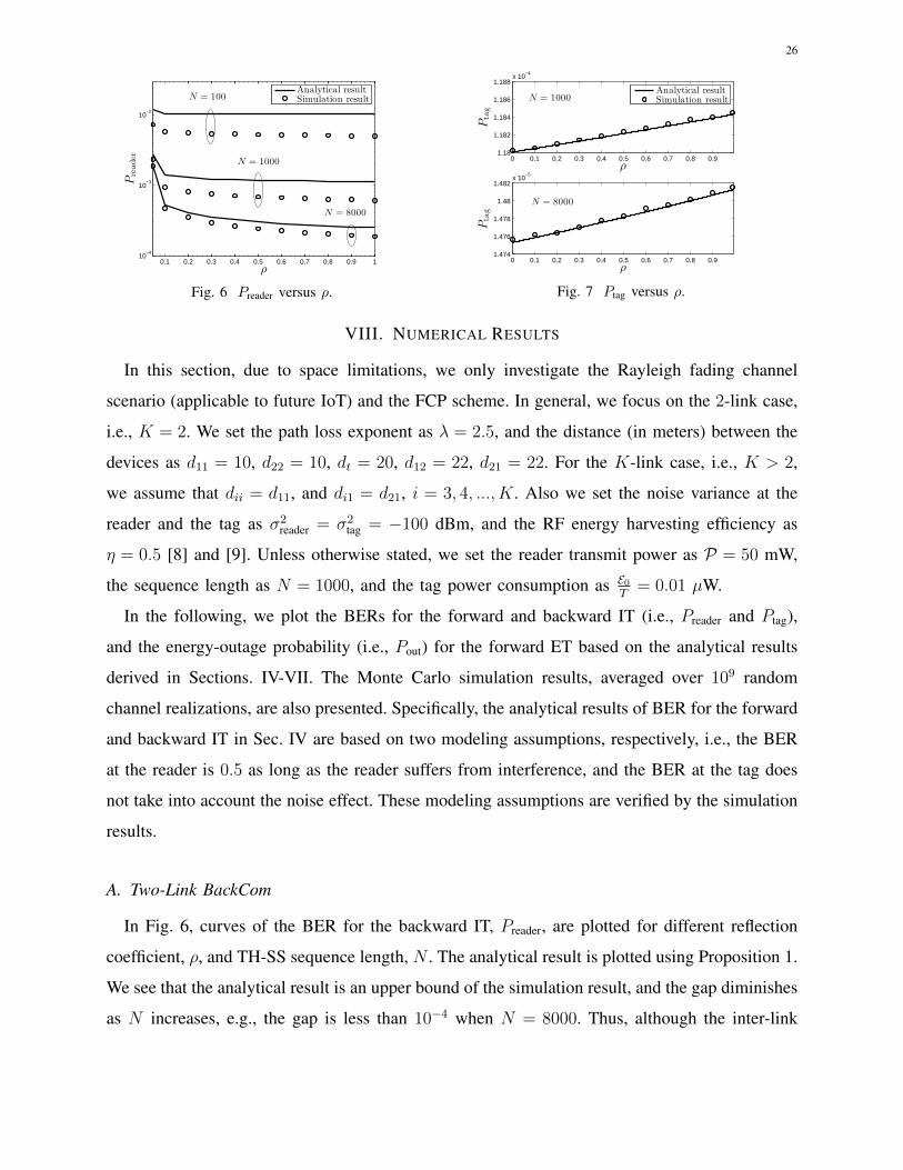
In this section, due to space limitations, we only investigate the Rayleigh fading channel
scenario (applicable to future IoT) and the FCP scheme. In general, we focus on the 2-link case,
i.e., K = 2. We set the path loss exponent as λ = 2.5, and the distance (in meters) between the
devices as d11 = 10, d22 = 10, dt = 20, d12 = 22, d21 = 22. For the K-link case, i.e., K > 2,
we assume that dii = d11, and di1 = d21, i = 3, 4, ..., K. Also we set the noise variance at the
reader and the tag as σ2reader = σ2
tag = −100 dBm, and the RF energy harvesting efficiency as
η = 0.5 [8] and [9]. Unless otherwise stated, we set the reader transmit power as P = 50 mW,
the sequence length as N = 1000, and the tag power consumption as E0T
= 0.01 µW.
In the following, we plot the BERs for the forward and backward IT (i.e., Preader and Ptag),
and the energy-outage probability (i.e., Pout) for the forward ET based on the analytical results
derived in Sections. IV-VII. The Monte Carlo simulation results, averaged over 109 random
channel realizations, are also presented. Specifically, the analytical results of BER for the forward
and backward IT in Sec. IV are based on two modeling assumptions, respectively, i.e., the BER
at the reader is 0.5 as long as the reader suffers from interference, and the BER at the tag does
not take into account the noise effect. These modeling assumptions are verified by the simulation
results.
A. Two-Link BackCom
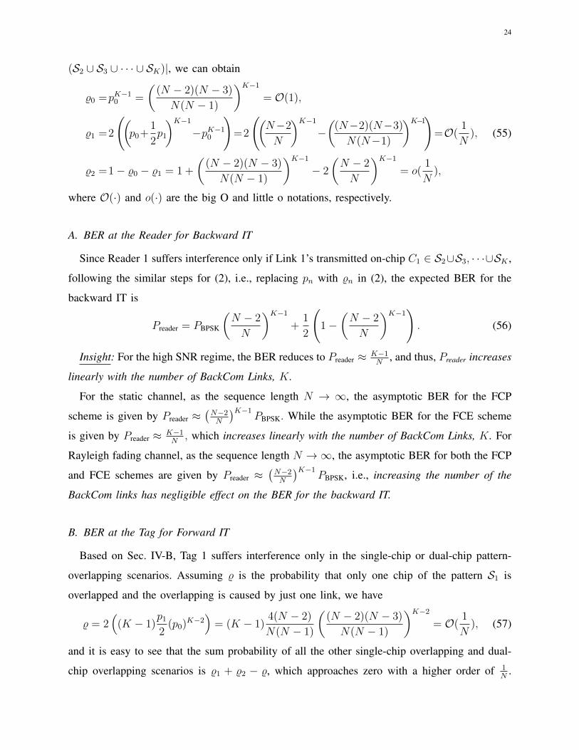
In Fig. 6, curves of the BER for the backward IT, Preader, are plotted for different reflection
coefficient, ρ, and TH-SS sequence length, N . The analytical result is plotted using Proposition 1.
We see that the analytical result is an upper bound of the simulation result, and the gap diminishes
as N increases, e.g., the gap is less than 10−4 when N = 8000. Thus, although the inter-link
27
0 0.2 0.4 0.6 0.8 110
−4
10−3
10−2
10−1
100
ρ
Pout
Analytical results
Simulation results
N = 8000
N = 1000
N = 100
Fig. 8 Pout versus ρ.
0 0.2 0.4 0.6 0.8 110
−4
10−3
10−2
10−1
β
Pasyn
reader
Analytical resultSimulation resultN = 100
N = 1000
N = 8000
Fig. 9 P asynreader versus β.
interference may not be fatal, i.e., inducing a BER of 0.5 at the reader, the analytical result is
a tight upper bound especially when N is large.
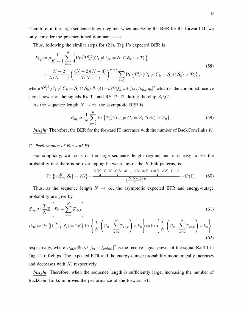
In Fig. 7, curves of the BER for the forward IT, Ptag, are plotted for different ρ and N . The
analytical result is plotted using Proposition 3. We see that the analytical results perfectly match
the simulation results, which verifies that the noise effect of the forward BER is negligible under
the practical settings.
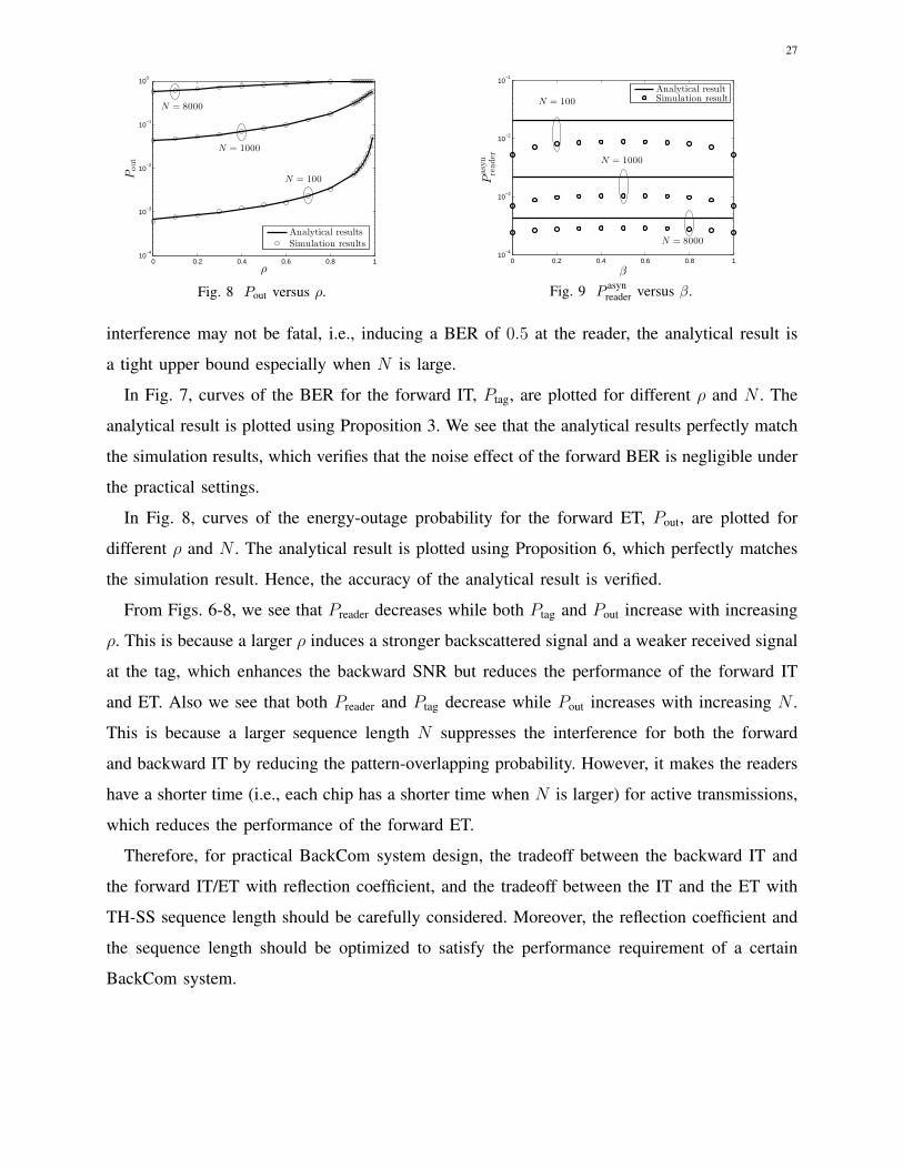
In Fig. 8, curves of the energy-outage probability for the forward ET, Pout, are plotted for
different ρ and N . The analytical result is plotted using Proposition 6, which perfectly matches
the simulation result. Hence, the accuracy of the analytical result is verified.
From Figs. 6-8, we see that Preader decreases while both Ptag and Pout increase with increasing
ρ. This is because a larger ρ induces a stronger backscattered signal and a weaker received signal
at the tag, which enhances the backward SNR but reduces the performance of the forward IT
and ET. Also we see that both Preader and Ptag decrease while Pout increases with increasing N .
This is because a larger sequence length N suppresses the interference for both the forward
and backward IT by reducing the pattern-overlapping probability. However, it makes the readers
have a shorter time (i.e., each chip has a shorter time when N is larger) for active transmissions,
which reduces the performance of the forward ET.
Therefore, for practical BackCom system design, the tradeoff between the backward IT and
the forward IT/ET with reflection coefficient, and the tradeoff between the IT and the ET with
TH-SS sequence length should be carefully considered. Moreover, the reflection coefficient and
the sequence length should be optimized to satisfy the performance requirement of a certain
BackCom system.
28
0 0.2 0.4 0.6 0.8 1
10−3.99
10−3.98
β
Pasyn
tag
Analytical result
Simulation result
0 0.2 0.4 0.6 0.8 1
10−4.89
10−4.88
β
Pasyn
tag
N = 1000
N = 8000
Fig. 10 P asyntag versus β.
2 3 4 5 6 7 8 9 1010
−4
10−3
10−2
10−1
K
Preader
Analytical result
Simulation result
N = 100
N = 1000
N = 8000
Fig. 11 Preader versus K.
B. Asynchronous BackCom
In Fig. 9, curves of the BER for the backward IT, P asynreader, are plotted for different delay offset,
β, and sequence length, N . The analytical result is plotted using (42). We see that the analytical
result is an upper bound of the simulation result, and the gap diminishes quickly as N increases,
e.g., the gap is about 10−3 when N = 1000, and is about 10−4 when N = 8000. From the
simulation result, we see that the BER for the backward IT is mostly affected when the delay
offset caused by chip asynchronization is equal to a half chip duration. The influence on the
BER caused by asynchronous transmissions is negligible when N is sufficiently large, i.e., the
BER is almost the same with β = 0 and 0.5, when N = 8000. Therefore, although the analytical
result is based on the assumption that the BER is the same no matter what the delay offset is,
the result is a tight upper bound especially when N is large.
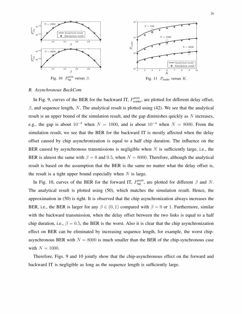
In Fig. 10, curves of the BER for the forward IT, P asyntag , are plotted for different β and N .
The analytical result is plotted using (50), which matches the simulation result. Hence, the
approximation in (50) is tight. It is observed that the chip asynchronization always increases the
BER, i.e., the BER is larger for any β ∈ (0, 1) compared with β = 0 or 1. Furthermore, similar
with the backward transmission, when the delay offset between the two links is equal to a half
chip duration, i.e., β = 0.5, the BER is the worst. Also it is clear that the chip asynchronization
effect on BER can be eliminated by increasing sequence length, for example, the worst chip-
asynchronous BER with N = 8000 is much smaller than the BER of the chip-synchronous case
with N = 1000.
Therefore, Figs. 9 and 10 jointly show that the chip-asynchronous effect on the forward and
backward IT is negligible as long as the sequence length is sufficiently large.

29
2 3 4 5 6 7 8 9 1010
−5
10−4
10−3
10−2
K
Ptag
Analytical result
Simulation result
N = 100
N = 1000
N = 8000
Fig. 12 Ptag versus K.
2 3 4 5 6 7 8 9 1010
−8
10−7
10−6
10−5
10−4
10−3
10−2
10−1
100
K
Pout
Analytical result
Simulation result
N = 100
N = 1000
N = 8000
Fig. 13 Pout versus K.
C. K-Link BackCom
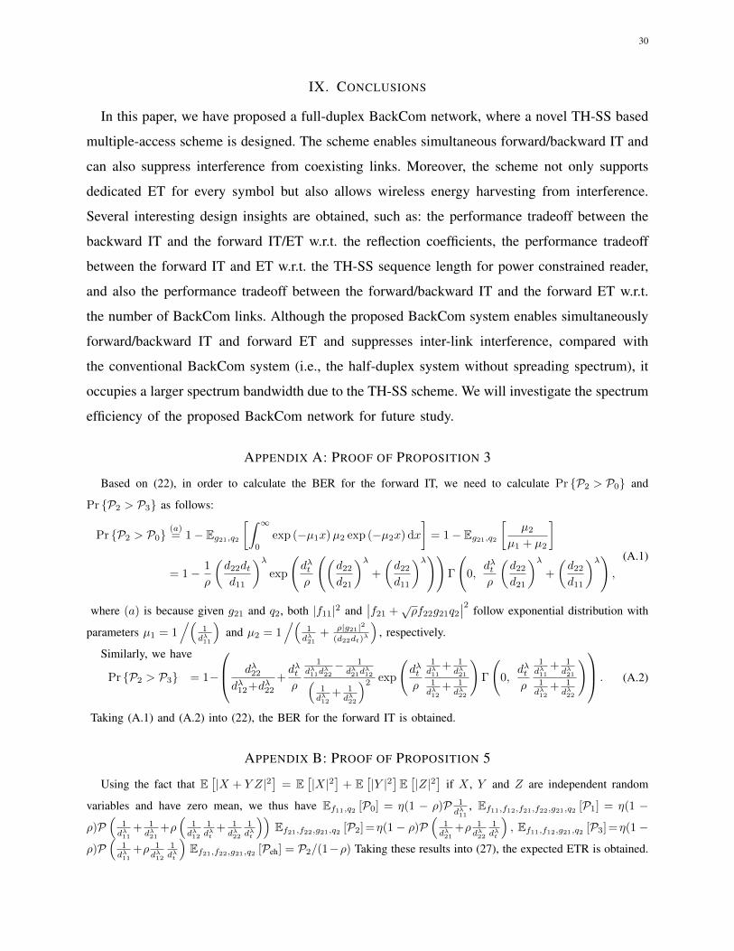
In Fig. 11, curves of Preader are plotted for different number of BackCom links, K, and different
sequence length, N . The analytical result is plotted using (56), which is an upper bound of the
accurate result since it assumes a BER of 0.5 when the interference occurs at the reader. We see
that the analytical result is a tight upper bound of the simulation result, and the gap diminishes
with the increasing sequence length and number of BackCom links. Also we see that Preader
increases with K, which is mainly because more BackCom links make the backward IT more
likely to suffer from interference. For a fixed N , the BER deteriorates as the number of BackCom
links becomes large, and can even become close to 0.5, when the interference occurs.
In Fig. 12, curves of Ptag are plotted for different K and N . The analytical result is plotted
using (58), which is a lower bound since it only takes into account the dominant term for a large
N . We see that the analytical result is a tight lower bound of the simulation result. Also we see
that Ptag increases with K, since more BackCom links make the backward IT more likely to
suffer from interference, and the interference is stronger when it occurs.
In Fig. 13, curves of the energy-outage probability, Pout, are plotted for different K and N .
The analytical result is plotted using (62), which is a lower bound since it only takes into account
the dominant term for a large N . We see that the analytical result is a tight lower bound of the
simulation result. Also we see that Pout decreases with K, since a large number of BackCom
links increases the harvested energy at the tag due to the multi-reader transmissions.
Figs. 11-13 jointly show the performance tradeoff between the IT and the ET with the
number of BackCom links. Thus, for practical BackCom network design, this tradeoff should
be carefully considered, and the number of BackCom links should be optimized to satisfy both
the performance requirement of IT and ET.
30
IX. CONCLUSIONS
In this paper, we have proposed a full-duplex BackCom network, where a novel TH-SS based
multiple-access scheme is designed. The scheme enables simultaneous forward/backward IT and
can also suppress interference from coexisting links. Moreover, the scheme not only supports
dedicated ET for every symbol but also allows wireless energy harvesting from interference.
Several interesting design insights are obtained, such as: the performance tradeoff between the
backward IT and the forward IT/ET w.r.t. the reflection coefficients, the performance tradeoff
between the forward IT and ET w.r.t. the TH-SS sequence length for power constrained reader,
and also the performance tradeoff between the forward/backward IT and the forward ET w.r.t.
the number of BackCom links. Although the proposed BackCom system enables simultaneously
forward/backward IT and forward ET and suppresses inter-link interference, compared with
the conventional BackCom system (i.e., the half-duplex system without spreading spectrum), it
occupies a larger spectrum bandwidth due to the TH-SS scheme. We will investigate the spectrum
efficiency of the proposed BackCom network for future study.
APPENDIX A: PROOF OF PROPOSITION 3
Based on (22), in order to calculate the BER for the forward IT, we need to calculate Pr {P2 > P0} and
Pr {P2 > P3} as follows:
Pr {P2 > P0}(a)= 1− Eg21,q2
[∫ ∞0
exp (−µ1x)µ2 exp (−µ2x) dx
]= 1− Eg21,q2
[µ2
µ1 + µ2
]= 1− 1
ρ
(d22dtd11
)λexp
(dλtρ
((d22
d21
)λ+
(d22
d11
)λ))Γ
(0,
dλtρ
(d22
d21
)λ+
(d22
d11
)λ),
(A.1)
where (a) is because given g21 and q2, both |f11|2 and∣∣f21 +
√ρf22g21q2
∣∣2 follow exponential distribution with
parameters µ1 = 1/(
1dλ11
)and µ2 = 1
/(1dλ21
+ ρ|g21|2
(d22dt)λ
), respectively.
Similarly, we have
Pr {P2 > P3} = 1−
dλ22
dλ12+dλ22
+dλtρ
1dλ11d
λ22− 1dλ21d
λ12(
1dλ12
+ 1dλ22
)2 exp
(dλtρ
1dλ11
+ 1dλ21
1dλ12
+ 1dλ22
)Γ
(0,
dλtρ
1dλ11
+ 1dλ21
1dλ12
+ 1dλ22
) . (A.2)
Taking (A.1) and (A.2) into (22), the BER for the forward IT is obtained.
APPENDIX B: PROOF OF PROPOSITION 5
Using the fact that E[|X + Y Z|2
]= E
[|X|2
]+ E
[|Y |2
]E[|Z|2
]if X , Y and Z are independent random
variables and have zero mean, we thus have Ef11,q2 [P0] = η(1 − ρ)P 1dλ11
, Ef11,f12,f21,f22,g21,q2 [P1] = η(1 −ρ)P
(1dλ11
+ 1dλ21
+ρ(
1dλ12
1dλt
+ 1dλ22
1dλt
))Ef21,f22,g21,q2 [P2] =η(1 − ρ)P
(1dλ21
+ρ 1dλ22
1dλt
), Ef11,f12,g21,q2 [P3] =η(1 −
ρ)P(
1dλ11
+ρ 1dλ12
1dλt
)Ef21,f22,g21,q2 [Peh] = P2/(1−ρ) Taking these results into (27), the expected ETR is obtained.

31
APPENDIX C: PROOF OF PROPOSITION 6
Given g21 and q2, then P0/(ηP) and Peh/(ηP) are independent with each other and follow exponential distri-
bution with mean parameters (1− ρ) 1dλ11
and(
1dλ21
+ ρ 1dλ22
1dλt|g21|2
), respectively. Thus, we have
Pr
{T
N(P0 + Peh) < E0
}= Eg21,q2
[Pr
{(P0 + Peh)
ηP <NE0ηPT
∣∣∣∣ g21, q2
}]
= 1− Eg21
(1− ρ) 1
dλ11exp
(− Ξ
(1−ρ) 1
dλ11
)−(
1dλ21
+ ρ 1dλ22
1dλt|g21|2
)exp
− Ξ(1
dλ21
+ρ 1
dλ22
1
dλt
|g21|2)
(1− ρ) 1dλ11−(
1dλ21
+ ρ 1dλ22
1dλt|g21|2
)
= M
((1− ρ)
1
dλ11
, 0,1
dλ21
, ρ1
dλ22
1
dλt
).
(C.1)
where Ξ , NE0ηPT , and function M(·, ·, ·, ·) is defined in (34). Similarly, we can obtain Pr
{TN (P0 + P2) < E0
},
Pr{TN (P3 + Peh) < E0
}, Pr
{TN (P3 + P2) < E0
}, Pr
{TNP1<E0
}. Taking these results and (3), (C.1), and (34)
into (32), the energy-outage probability is obtained.
REFERENCES
[1] V. Chawla and D. S. Ha, “An overview of passive RFID,” IEEE Commun. Mag., vol. 45, no. 9, pp. 11–17, Sep. 2007.
[2] C. Boyer and S. Roy, “Backscatter communication and RFID: Coding, energy, and MIMO analysis,” IEEE Trans. Commun.,
vol. 62, no. 3, pp. 770–785, Mar. 2014.
[3] A. Bletsas, S. Siachalou, and J. N. Sahalos, “Anti-collision backscatter sensor networks,” IEEE Trans. Wireless Commun.,
vol. 8, no. 10, pp. 5018–5029, Oct. 2009.
[4] J. Kimionis, A. Bletsas, and J. N. Sahalos, “Increased range bistatic scatter radio,” IEEE Trans. Commun., vol. 62, no. 3,
pp. 1091–1104, Mar. 2014.
[5] A. Alma’aitah, H. S. Hassanein, and M. Ibnkahla, “Tag modulation silencing: Design and application in RFID anti-collision
protocols,” IEEE Trans. Commun., vol. 62, no. 11, pp. 4068–4079, Nov. 2014.
[6] J. Wang, H. Hassanieh, D. Katabi, and P. Indyk, “Efficient and reliable low-power backscatter networks,” in Proc. ACM
SIGCOMM, 2012, pp. 61–72.
[7] K. Han and K. Huang, “Wirelessly powered backscatter communication networks: Modeling, coverage and capacity,” to
appear in IEEE Trans. Wireless Commun., 2017.
[8] K. Huang and X. Zhou, “Cutting the last wires for mobile communications by microwave power transfer,” IEEE Commun.
Mag., vol. 53, no. 6, pp. 86–93, Jun. 2015.
[9] S. Bi, C. Ho, and R. Zhang, “Wireless powered communication: Opportunities and challenges,” IEEE Commun. Mag.,
vol. 53, no. 4, pp. 117–125, Apr. 2015.
[10] G. Yang, C. K. Ho, and Y. L. Guan, “Multi-antenna wireless energy transfer for backscatter communication systems,”
IEEE J. Sel. Areas Commun., vol. 33, no. 12, pp. 2974–2987, Dec. 2015.
[11] S. Lee, L. Liu, and R. Zhang, “Collaborative wireless energy and information transfer in interference channel,” IEEE
Trans. Wireless Commun., vol. 14, no. 1, pp. 545–557, Jan. 2015.
[12] V. Liu, A. Parks, V. Talla, S. Gollakota, D. Wetherall, and J. R. Smith, “Ambient backscatter: Wireless communication out
of thin air,” in Proc. ACM SIGCOMM, 2013, pp. 39–50.
32
[13] V. Liu, V. Talla, and S. Gollakota, “Enabling instantaneous feedback with full-duplex backscatter,” in Proc. ACM MobiCom,
2014, pp. 67–78.
[14] M. Z. Win, R. A. Scholtz et al., “Ultra-wide bandwidth time-hopping spread-spectrum impulse radio for wireless multiple-
access communications,” IEEE Trans. Commun., vol. 48, no. 4, pp. 679–689, Apr. 2000.
[15] D. Dardari, R. D. Errico, C. Roblin, A. Sibille, and M. Z. Win, “Ultrawide bandwidth RFID: Next generation?” Proc.
IEEE, vol. 98, no. 9, pp. 1570–1582, Sep. 2010.
[16] A. Al-Fuqaha, M. Guizani, M. Mohammadi, M. Aledhari, and M. Ayyash, “Internet of Things: A survey on enabling
technologies, protocols, and applications,” IEEE Commun. Surveys Tuts., vol. 17, no. 4, pp. 2347–2376, Fourth Quarter
2015.
[17] A. Sabharwal, P. Schniter, D. Guo, D. Bliss, S. Rangarajan, and R. Wichman, “In-band full-duplex wireless: Challenges
and opportunities,” IEEE J. Sel. Areas Commun., vol. 32, no. 9, pp. 1637–1652, Sept 2014.
[18] S. Verdu and S. Shamai, “Spectral efficiency of CDMA with random spreading,” IEEE Trans. Inf. Theory, vol. 45, no. 2,
pp. 622–640, Feb. 1999.
[19] H. Urkowitz, “Energy detection of unknown deterministic signals,” Proc. IEEE, vol. 55, no. 4, pp. 523–531, Apr. 1967.
[20] D. Bharadia, E. McMilin, and S. Katti, “Full duplex radios,” in Proc. ACM SIGCOMM, 2013, pp. 375–386.
[21] M. Abramowitz and I. A. Stegun, Handbook of mathematical functions: with formulas, graphs, and mathematical tables.
Dover Publications, Inc., 1970.