Full-Adder The Binary Adder - Imperial College London 9 - adders... · Full-Adder E4.20 Digital IC...
10
Topic 9 - 1 Nov-22-10 E4.20 Digital IC Design © Prentice Hall Topic 9 Arithmetic Circuits & Datapaths Peter Cheung Department of Electrical & Electronic Engineering Imperial College London URL: www.ee.ic.ac.uk/pcheung/ E-mail: [email protected] Topic 9 - 2 Nov-22-10 E4.20 Digital IC Design © Prentice Hall Bit-Sliced Design Topic 9 - 3 Nov-22-10 E4.20 Digital IC Design © Prentice Hall Full-Adder Topic 9 - 4 Nov-22-10 E4.20 Digital IC Design © Prentice Hall The Binary Adder
Transcript of Full-Adder The Binary Adder - Imperial College London 9 - adders... · Full-Adder E4.20 Digital IC...

Topic 9 - 1 Nov-22-10 E4.20 Digital IC Design © Prentice Hall
Topic 9 Arithmetic Circuits &
Datapaths
Peter Cheung Department of Electrical & Electronic Engineering
Imperial College London
URL: www.ee.ic.ac.uk/pcheung/ E-mail: [email protected]
Topic 9 - 2 Nov-22-10 E4.20 Digital IC Design © Prentice Hall
Bit-Sliced Design
Topic 9 - 3 Nov-22-10 E4.20 Digital IC Design © Prentice Hall
Full-Adder
Topic 9 - 4 Nov-22-10 E4.20 Digital IC Design © Prentice Hall
The Binary Adder

Topic 9 - 5 Nov-22-10 E4.20 Digital IC Design © Prentice Hall
Express Sum and Carry as a function of P, G, D
Define 3 new variable which ONLY depend on A, B Generate (G) = AB Propagate (P) = A ⊕ B Delete = A B
Can also derive expressions for S and C o based on D and P
Topic 9 - 6 Nov-22-10 E4.20 Digital IC Design © Prentice Hall
The Ripple-Carry Adder
Topic 9 - 7 Nov-22-10 E4.20 Digital IC Design © Prentice Hall
Complimentary Static CMOS Full Adder
Topic 9 - 8 Nov-22-10 E4.20 Digital IC Design © Prentice Hall
Inversion Property

Topic 9 - 9 Nov-22-10 E4.20 Digital IC Design © Prentice Hall
Minimize Critical Path by Reducing Inverting Stages
Topic 9 - 10 Nov-22-10 E4.20 Digital IC Design © Prentice Hall
The better structure: the Mirror Adder
Generate (G) = AB Propagate (P) = A ⊕ B Delete = A B
Topic 9 - 11 Nov-22-10 E4.20 Digital IC Design © Prentice Hall
The Mirror Adder
• The NMOS and PMOS chains are completely symmetrical. This guarantees identical rising and falling transitions if the NMOS and PMOS devices are properly sized. A maximum of two series transistors can be observed in the carry-generation circuitry.
• When laying out the cell, the most critical issue is the minimization of the capacitance at node Co. The reduction of the diffusion capacitances is particularly important.
• The capacitance at node Co is composed of four diffusion capacitances, two internal gate capacitances, and six gate capacitances in the connecting adder cell .
• The transistors connected to Ci are placed closest to the output. • Only the transistors in the carry stage have to be optimized for optimal speed. All transistors in the sum stage can be minimal size.
Topic 9 - 12 Nov-22-10 E4.20 Digital IC Design © Prentice Hall
Quasi-Clocked Adder

Topic 9 - 13 Nov-22-10 E4.20 Digital IC Design © Prentice Hall
Manchester Carry Chain
Topic 9 - 14 Nov-22-10 E4.20 Digital IC Design © Prentice Hall
Sizing Manchester Carry Chain
Topic 9 - 15 Nov-22-10 E4.20 Digital IC Design © Prentice Hall
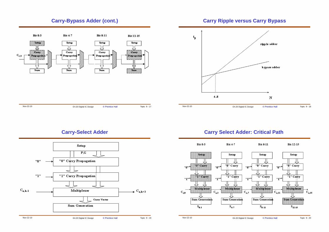
Carry-Bypass Adder
Topic 9 - 16 Nov-22-10 E4.20 Digital IC Design © Prentice Hall
Manchester-Carry Implementation
Topic 9 - 17 Nov-22-10 E4.20 Digital IC Design © Prentice Hall
Carry-Bypass Adder (cont.)
Topic 9 - 18 Nov-22-10 E4.20 Digital IC Design © Prentice Hall
Carry Ripple versus Carry Bypass
Topic 9 - 19 Nov-22-10 E4.20 Digital IC Design © Prentice Hall
Carry-Select Adder
Topic 9 - 20 Nov-22-10 E4.20 Digital IC Design © Prentice Hall
Carry Select Adder: Critical Path

Topic 9 - 21 Nov-22-10 E4.20 Digital IC Design © Prentice Hall
Linear Carry Select
Topic 9 - 22 Nov-22-10 E4.20 Digital IC Design © Prentice Hall
Square Root Carry Select
Topic 9 - 23 Nov-22-10 E4.20 Digital IC Design © Prentice Hall
Adder Delays - Comparison
Topic 9 - 24 Nov-22-10 E4.20 Digital IC Design © Prentice Hall
LookAhead - Basic Idea

Topic 9 - 25 Nov-22-10 E4.20 Digital IC Design © Prentice Hall
Look-Ahead: Topology
Topic 9 - 26 Nov-22-10 E4.20 Digital IC Design © Prentice Hall
The Array Multiplier
Topic 9 - 27 Nov-22-10 E4.20 Digital IC Design © Prentice Hall
The MxN Array Multiplier — Critical Path
Critical Path 1 & 2
Topic 9 - 28 Nov-22-10 E4.20 Digital IC Design © Prentice Hall
Carry-Save Multiplier

Topic 9 - 29 Nov-22-10 E4.20 Digital IC Design © Prentice Hall
Adder Cells in Array Multiplier
Topic 9 - 30 Nov-22-10 E4.20 Digital IC Design © Prentice Hall
Multiplier Floorplan
Topic 9 - 31 Nov-22-10 E4.20 Digital IC Design © Prentice Hall
Multipliers —Summary
Topic 9 - 32 Nov-22-10 E4.20 Digital IC Design © Prentice Hall
The Binary Shifter

Topic 9 - 33 Nov-22-10 E4.20 Digital IC Design © Prentice Hall
The Barrel Shifter
Area Dominated by Wiring Topic 9 - 34 Nov-22-10 E4.20 Digital IC Design © Prentice Hall
4x4 barrel shifter
Widthbarrel ~ 2 pm M
Topic 9 - 35 Nov-22-10 E4.20 Digital IC Design © Prentice Hall
Logarithmic Shifter
Topic 9 - 36 Nov-22-10 E4.20 Digital IC Design © Prentice Hall
A 3
A 2
A 1
A 0
Out3
Out2
Out1
Out0
0-7 bit Logarithmic Shifter

Topic 9 - 37 Nov-22-10 E4.20 Digital IC Design © Prentice Hall
Design as a Trade-Off
Topic 9 - 38 Nov-22-10 E4.20 Digital IC Design © Prentice Hall
Layout Strategies for Bit-Sliced Datapaths
Topic 9 - 39 Nov-22-10 E4.20 Digital IC Design © Prentice Hall
Layout of Bit-sliced Datapaths
Topic 9 - 40 Nov-22-10 E4.20 Digital IC Design © Prentice Hall
Layout of Bit-sliced Datapaths