FUJITSU SEMICONDUCTOR LIMITED · ... air traffic control, mass transport ... management for system...
16
Power Management ICs Specifications are subject to change without notice. For further information please contact each office. All Rights Reserved. The contents of this document are subject to change without notice. Customers are advised to consult with sales representatives before ordering. The information, such as descriptions of function and application circuit examples, in this document are presented solely for the purpose of reference to show examples of operations and uses of FUJITSU SEMICONDUCTOR device; FUJITSU SEMICONDUCTOR does not warrant proper operation of the device with respect to use based on such information. When you develop equipment incorporating the device based on such information, you must assume any responsibility arising out of such use of the information. FUJITSU SEMICONDUCTOR assumes no liability for any damages whatsoever arising out of the use of the information. Any information in this document, including descriptions of function and schematic diagrams, shall not be construed as license of the use or exercise of any intellectual property right, such as patent right or copyright, or any other right of FUJITSU SEMICONDUCTOR or any third party or does FUJITSU SEMICONDUCTOR warrant non-infringement of any third-party's intellectual property right or other right by using such information. FUJITSU SEMICONDUCTOR assumes no liability for any infringement of the intellectual property rights or other rights of third parties which would result from the use of information contained herein. The products described in this document are designed, developed and manufactured as contemplated for general use, including without limitation, ordinary industrial use, general office use, personal use, and household use, but are not designed, developed and manufactured as contemplated (1) for use accompanying fatal risks or dangers that, unless extremely high safety is secured, could have a serious effect to the public, and could lead directly to death, personal injury, severe physical damage or other loss (i.e., nuclear reaction control in nuclear facility, aircraft flight control, air traffic control, mass transport control, medical life support system, missile launch control in weapon system), or (2) for use requiring extremely high reliability (i.e., submersible repeater and artificial satellite). Please note that FUJITSU SEMICONDUCTOR will not be liable against you and/or any third party for any claims or damages arising in connection with above-mentioned uses of the products. Any semiconductor devices have an inherent chance of failure. You must protect against injury, damage or loss from such failures by incorporating safety design measures into your facility and equipment such as redundancy, fire protection, and prevention of overcurrent levels and other abnormal operating conditions. Exportation/release of any products described in this document may require necessary procedures in accordance with the regulations of the Foreign Exchange and Foreign Trade Control Law of Japan and/or US export control laws. The company names and brand names herein are the trademarks or registered trademarks of their respective owners. FUJITSU SEMICONDUCTOR LIMITED Nomura Fudosan Shin-yokohama Bldg. 10-23, Shin-yokohama 2-Chome, Kohoku-ku Yokohama Kanagawa 222-0033, Japan Tel: +81-45-415-5858 http://jp.fujitsu.com/fsl/en/ © 1998-2011 FUJITSU SEMICONDUCTOR LIMITED Printed in Japan AD04-00006-17E July, 2011 Edited: Sales Promotion Department For further information please contact: North and South America FUJITSU SEMICONDUCTOR AMERICA, INC. 1250 E. Arques Avenue, M/S 333 Sunnyvale, CA 94085-5401, U.S.A. Tel: +1-408-737-5600 Fax: +1-408-737-5999 http://us.fujitsu.com/micro/ Europe FUJITSU SEMICONDUCTOR EUROPE GmbH Pittlerstrasse 47, 63225 Langen, Germany Tel: +49-6103-690-0 Fax: +49-6103-690-122 http://emea.fujitsu.com/semiconductor/ Korea FUJITSU SEMICONDUCTOR KOREA LTD. 902 Kosmo Tower Building, 1002 Daechi-Dong, Gangnam-Gu, Seoul 135-280, Republic of Korea Tel: +82-2-3484-7100 Fax: +82-2-3484-7111 http://kr.fujitsu.com/fsk/ Asia Pacific FUJITSU SEMICONDUCTOR ASIA PTE. LTD. 151 Lorong Chuan, #05-08 New Tech Park 556741 Singapore Tel : +65-6281-0770 Fax : +65-6281-0220 http://sg.fujitsu.com/semiconductor/ FUJITSU SEMICONDUCTOR SHANGHAI CO., LTD. Rm. 3102, Bund Center, No.222 Yan An Road (E), Shanghai 200002, China Tel : +86-21-6146-3688 Fax : +86-21-6335-1605 http://cn.fujitsu.com/fss/ FUJITSU SEMICONDUCTOR PACIFIC ASIA LTD. 10/F., World Commerce Centre, 11 Canton Road, Tsimshatsui, Kowloon, Hong Kong Tel : +852-2377-0226 Fax : +852-2376-3269 http://cn.fujitsu.com/fsp/ 2011.7 FUJITSU SEMICONDUCTOR
Transcript of FUJITSU SEMICONDUCTOR LIMITED · ... air traffic control, mass transport ... management for system...

Power Management ICs
Specifications are subject to change without notice. For further information please contact each office.
All Rights Reserved.The contents of this document are subject to change without notice.Customers are advised to consult with sales representatives before ordering.The information, such as descriptions of function and application circuit examples, in this document are presented solely for the purpose of reference to show examples of operations and uses of FUJITSU SEMICONDUCTOR device; FUJITSU SEMICONDUCTOR does not warrant proper operation of the device with respect to use based on such information. When you develop equipment incorporating the device based on such information, you must assume any responsibility arising out of such use of the information.FUJITSU SEMICONDUCTOR assumes no liability for any damages whatsoever arising out of the use of the information.Any information in this document, including descriptions of function and schematic diagrams, shall not be construed as license of the use or exercise of any intellectual property right, such as patent right or copyright, or any other right of FUJITSU SEMICONDUCTOR or any third party or does FUJITSU SEMICONDUCTOR warrant non-infringement of any third-party's intellectual property right or other right by using such information. FUJITSU SEMICONDUCTOR assumes no liability for any infringement of the intellectual property rights or other rights of third parties which would result from the use of information contained herein.The products described in this document are designed, developed and manufactured as contemplated for general use, including without limitation, ordinary industrial use, general office use, personal use, and household use, but are not designed, developed and manufactured as contemplated (1) for use accompanying fatal risks or dangers that, unless extremely high safety is secured, could have a serious effect to the public, and could lead directly to death, personal injury, severe physical damage or other loss (i.e., nuclear reaction control in nuclear facility, aircraft flight control, air traffic control, mass transport control, medical life support system, missile launch control in weapon system), or (2) for use requiring extremely high reliability (i.e., submersible repeater and artificial satellite).Please note that FUJITSU SEMICONDUCTOR will not be liable against you and/or any third party for any claims or damages arising in connection with above-mentioned uses of the products.Any semiconductor devices have an inherent chance of failure. You must protect against injury, damage or loss from such failures by incorporating safety design measures into your facility and equipment such as redundancy, fire protection, and prevention of overcurrent levels and other abnormal operating conditions.Exportation/release of any products described in this document may require necessary procedures in accordance with the regulations of the Foreign Exchange and Foreign Trade Control Law of Japan and/or US export control laws.The company names and brand names herein are the trademarks or registered trademarks of their respective owners.
FUJITSU SEMICONDUCTOR LIMITEDNomura Fudosan Shin-yokohama Bldg. 10-23, Shin-yokohama 2-Chome,Kohoku-ku Yokohama Kanagawa 222-0033, JapanTel: +81-45-415-5858http://jp.fujitsu.com/fsl/en/
© 1998-2011 FUJITSU SEMICONDUCTOR LIMITED Printed in JapanAD04-00006-17E July, 2011Edited: Sales Promotion Department
For further information please contact:
North and South AmericaFUJITSU SEMICONDUCTOR AMERICA, INC.1250 E. Arques Avenue, M/S 333Sunnyvale, CA 94085-5401, U.S.A.Tel: +1-408-737-5600 Fax: +1-408-737-5999http://us.fujitsu.com/micro/
EuropeFUJITSU SEMICONDUCTOR EUROPE GmbHPittlerstrasse 47, 63225 Langen, GermanyTel: +49-6103-690-0 Fax: +49-6103-690-122http://emea.fujitsu.com/semiconductor/
KoreaFUJITSU SEMICONDUCTOR KOREA LTD.902 Kosmo Tower Building, 1002 Daechi-Dong,Gangnam-Gu, Seoul 135-280, Republic of KoreaTel: +82-2-3484-7100 Fax: +82-2-3484-7111http://kr.fujitsu.com/fsk/
Asia PacificFUJITSU SEMICONDUCTOR ASIA PTE. LTD.151 Lorong Chuan, #05-08 New Tech Park 556741 SingaporeTel : +65-6281-0770 Fax : +65-6281-0220http://sg.fujitsu.com/semiconductor/
FUJITSU SEMICONDUCTOR SHANGHAI CO., LTD.Rm. 3102, Bund Center, No.222 Yan An Road (E),Shanghai 200002, ChinaTel : +86-21-6146-3688 Fax : +86-21-6335-1605http://cn.fujitsu.com/fss/
FUJITSU SEMICONDUCTOR PACIFIC ASIA LTD.10/F., World Commerce Centre, 11 Canton Road,Tsimshatsui, Kowloon, Hong KongTel : +852-2377-0226 Fax : +852-2376-3269http://cn.fujitsu.com/fsp/
2011.7
FUJITSU SEMICONDUCTOR

FUJITSU Power Management IC1 FUJITSU Power Management IC 2
Saving Power-High efficiencySaving Power-High efficiency
Miniaturize-Small packaging-Reduce external
components
Miniaturize-Small packaging-Reduce external
components
Control topology-Ultra fast transient
responce-Low voltage output
Control topology-Ultra fast transient
responce-Low voltage output
Eco* device solutionEco* device solution
*Eco; An onomatopoeic word between Ecology and Economy.*Eco; An onomatopoeic word between Ecology and Economy.
Digital Network built on personal computer and digital home appliances are growing rapidly
in recent years. Multi-function electrical appliances are increasingly available making it
more convenient for family and society.
On the other hand, increasing use of various types of electrical equipment will result in
higher energy consumption. Global warming and environmental concern need to be addressed especially
when usage is expected to spread widely.
Hence, integrating more features into the products while maintaining high energy efficiency and
environmental friendliness have become more important for product development.
Fujitsu Semiconductor strives to contribute to green environment by developing power management ICs
focusing on attributes like; high power efficiency for saving power, miniaturize packaging,
reduce external components, and effective control technique
for fast transient response and lower output voltage.
ECO is in our SEMICONDUCTORsECO is in our SEMICONDUCTORs
7 to 10・13
11 to 13
14
18
15
18
16
18
17
15
3 to 5
6
25
26
26
27 to 28
29 to 30
19 to 20
21 to 22
23 to 24
Noteworthy Non-linear Hysteresis Control MethodAs a DC/DC Converter Control Method
Power Management IC for Portable Devices1-Channel DC/DC Converter + 1-Channel Low-Noise LDO + POR
DC/DC Converter ICs forCharging Li-ion Batteries in Notebook PCs
General-purpose DC/DC Converter
DC/DC Converter with Switching FET
DC/DC Converter with Switching FET + LDO
Power Supply for RF Power Amplifier
DC/DC Converter IC for System Power Supply
DC/DC Converter for LCD Panels
Charge Control
Power Voltage Monitoring Applications
Power Management Switches
AC/DC Converter
Lineup from Application
IC Lineup of DC/DC Converter
Lineup from Category
Product Analysis/Technical Analysis
Package
Evaluation Board
Search of Product and Document
Global Network
Table of Power Management ICs

FUJITSU Power Management IC3 FUJITSU Power Management IC 4
IP telephone power management ICIP telephone power management IC
Game machines power management ICGame machines power management IC
Printer power management ICPrinter power management IC
Application example
Application example
Application example
Application example
Application examplePortable device power management IC (GPS/PND/PMP)Portable device power management IC (GPS/PND/PMP)
Power overEthernet
Private IP telephone
Li-ion battery
1cell-Li-ion battery Charger
Switch
Boost
LCD panel
SolutionChip
Invert
Backlight driver
15V
26V
2.5V
1.2V
3.3V
5V13V-48V
12V
24V
5.0V
3.3V
1.2V
1.8V5.0V
3.3V
1.2V
-48V
Charger
-7.5V
3.3V
1.8V
PND: Personal Navigation Device, PMP: Portable Media Player
IEEE802.3af DC/DC
AC/DC
AC/DC
DC/DC
LED
Memory
Call control CPU
Audio CODEC DSP
LAN controller
DDR
White LED
System LSI
Flash memory
Head (Motor driver, etc.)
I/OCore
LSI
CPU
DDR2
LAN1394
ROM (Flash)
ASIC (image processing,compression, extension)
ASIC (CPU IF, DRAMC,BUSC, CPU perimeter, IF)
I/O power supplyCore power supply
Lineup from ApplicationProvided for different digital appliances from PC, cellular phones and communication networks to digital TV, digital cameras and DVC, power management ICs of Fujitsu Semiconductor combine state-of-the-art semiconductor design and production technology, system technology and application technology, and have risen to prominence as core technology of digital appliances.Combining the above advanced technology, Fujitsu offers power management IC featuring high performance, advanced functions and user-friendliness.
MB39C022L
MB39A136
1.2V1.8V
CMMBProcessor
LCD
PDM
SD/MMCBB
Memory
RF
PDM: Pulse Density Modulation
Application exampleNotebook computer power management ICNotebook computer power management IC
Mobile phone power management ICMobile phone power management IC
General-purpose DC/DC converter
For charging controlRecommended devices
Recommended devices
Recommended devicesRecommended devices
Power management switch
Monitoring of power supply voltage - MB3800 - MB39A135 - MB39A136 - MB39A130A - MB39A214 - MB39A202A
- MB39A134 - MB39A132A
- MB3800 - MB39A104 - MB39C011A
- MB39A135 - MB39A136
- MB39A130A - MB39A135
- MB39A136 - MB39A214
- MB39C011A - MB39C006A - MB39C014 - MB39C007
- MB39C015 - MB39A135 - MB39A136
- MB3771 - MB3773 - MB3793
- MB3841 - MB3842 - MB3845
Recommended device
- MB39C022
- MB39C006A - MB39C014 - MB39C316
- MB39C007 - MB39C015 - MB39C022

FUJITSU Power Management IC5 FUJITSU Power Management IC 6
Application example
Application example
Application example
General
General(SW FET)
LCD
For RF-PA
Charge ControlCharge Control
DC/DC+LDODC/DC+LDO
Output channels
Fujitsu Semiconductor provides various power management IC covering a vast range of specifications: the number of output channels ranges from 1 to 6 and the input voltage from 1.7V to 28V.
1ch : Loading number of channels
: Buck-conv.
: Buck/Boost-conv.
: Boost-conv.
: Invert-conv.
: Short-circuit protection
: Built-in switching FET
: Maximum load current per one channel (Recommended)
: Over-temperature protection circuit
: Overvoltage protection circuit
: Under-voltage protection circuit
: Overcurrent protection circuit
: Indication of function : Indication of no function : Internal FET : External FET(ex.)
Buck
B/B
Boost
Inv
FET
Buck
Buck
B/B
Boost
Inv
FET
Buck
SCP
SCP SCP
0.6A 4A
0.6A 4A
OTP
OVP
UVP
OCP
OTP
OVP
UVP
OCP
SCP
For SystemFor System
1.7V 4.5V 25.0V 28.0V7.0V2.5V 11.0V 18.0V15.0V5.5V Power supplyvoltage
*
*
MENU
1ch
2ch
3ch
4ch
6ch
*1: 3ch DC/DC+4ch LDO *2: 1ch DC/DC+1ch LDO *3: 2ch DC/DC+2ch LDO
MB39C316 *1
MB39C313AMB39C313B
MB39A123
MB3800
MB39A135
MB39C011A
MB39A136
MB39A104
MB39A112
MB39C014MB39C006A
MB39C022 *2
MB39C326
MB39C015MB39C007
MB39A134/MB39A132A
MB39A202A *3
MB39A214
MB39A130A *
Lineup from Application
1.8V
1.2V
3.3V
12VDDR2 SDRAM
I/O
Core
Flash memory
System LSI
AC/DC MB39A135
MB39A136
AC adapter
2.8V3.3V to 4.2V
1.2VLi-ion battery
DAC
MPU / SOC
Flash memory
MB39C015 USB
Explanation of a Functional Display
IC Lineup of DC/DC Converter
For 1-Seg TV and Mobile TVFor 1-Seg TV and Mobile TV
Smart phones and e-BooksSmart phones and e-Books
For digital home appliancesFor digital home appliances
*Bottom detection comparator method
1-cellLi-ion battery Cntl_Vout
Vout
BaseBand RFPowerAmp.
MB39C326
5-6V DC
Charger
Powermanagementfor system
Recommended devices
- MB39C006A - MB39C014 - MB39C007 - MB39C015 - MB39C316 - MB39C022
Recommended devices
- MB3800 - MB39C011A - MB39A104 - MB39A130A
- MB39A135 - MB39A136 - MB39A214 - MB39A202A
For LCD panel
- MB39C313A - MB39C313B
Recommended devices
- MB39C326

FUJITSU Power Management IC7 FUJITSU Power Management IC 8
VBIN
VB
REFIN
+INC
CUVP
-INC
ILIM
LSAT
CS
FB
VO
CB
OUT1
LX
A
OUT2
PGND
PGOOD
CTL
GNDVREF
B
COVP
VO
MB39A130A
A B
RT FSW VCC
TSSOP24
CTL
MB39A135CTL
GND
VCC
VB
RT
CS
FB
VIN
VIN
DRVL
DRVH
CB
LX
COMP
VREF
ILIM
VREF
VREF
A
A
1.8V
12V
CTL1
MB39A136
CTL1
GND
VCC
VB
RT
CS1
FB1
FB2
COMP2
VIN
VIN
VO2
DRVL2
DRVH2
CB2
LX2
VIN
VO1
DRVL1
DRVH1
CB1
LX1
COMP1
CTL2 CTL2
CS2
VREF
ILIM1
VREF
ILIM2
VREF
VREF
A
B
B
A
12V
1.2V
3.3V
TSSOP16
TSSOP24
1ch Buck B/B Boost Inv FET
OTP OVP UVPOCPSCP15A
2ch Buck B/B Boost Inv FET
OTP OVP UVPOCPSCP15A
1ch Buck B/B Boost Inv FET
OTP OVP UVPOCPSCP20A
TSSOP24
VIN
VIN
VIN
VIN
PGND
PGND
VOUT1
PGND
VOUT2
1.0 V, 7 A
1.8 V, 7 A
MB39A214
12 V
+
+
VOUT1
FB1
EN1
CS1
ILIM1
MODE
FREQ
VOUT2
EN2
CS2
EN2
EN1
C13
C12
C7
C8
R6
R4
R3-
2R
3-1
R1-
2R
1-1
R5
R2
GND
PGND
DRVL2
LX2
DRVH2
BST2
DRVL1
LX1
DRVH1
BST1
VB
VCC
ILIM2
FB2
3
19
18
1
24
23
12
13
14
15
21
2 1
Q3
Q3
Q1
5 6
7
43
7 82
1
Q1 5 64
3 L1
L2
C5
C1-
1
C1-
2
C2-
1
C3-
1
C6
C3-
2
C4-
1
C4-
3C
2-3
8
22
2
5
4
20
17
7
10
9
11
8
16
6
General-purpose DC/DC Converter
Application circuit example
MB39A130A Nch/Nch Synchronous Rectification 1-channel DC/DC Buck Converter IC
Application circuit example
MB39A135 Nch/Nch Synchronous Rectification 1-channel DC/DC Buck Converter IC
Application circuit example
MB39A136 Nch/Nch Synchronous Rectification 2-channel DC/DC Buck Converter IC
DescriptionMB39A135 is a Current mode Nch/Nch synchronous rectification
1-channel DC/DC buck converter IC. This IC has realized the
high-speed response, high efficiency and low ripple voltage by a
current mode system. It supports ceramic capacitors. It is suitable
for set miniaturization by using small package and compact coil
design enabled by adopting high frequency operation.
FeaturesWide range of power supply voltage: 4.5V to 25V
Selectable fixed PWM mode or automatic PFM/PWM mode
High frequency operation: 100kHz to 1.0MHz
Any output voltage setting by external resistor
Requires no flyback diode
Built-in soft-start circuit / Built-in soft-stop circuit
Substantial protective functions
ApplicationDigital TV, Digital AV devices etc.
Substantial protective functions
Application : P3,4,5
DescriptionMB39A136 is a Current mode Nch/Nch synchronous rectification
2-channel DC/DC buck converter IC. This IC has realized the
high-speed response, high efficiency and low ripple voltage by a
current mode system. It supports ceramic capacitors. It is suitable
for set miniaturization by using small package and compact coil
design enabled by adopting high frequency operation.
FeaturesWide range of power supply voltage: 4.5V to 25V
Selectable fixed PWM mode or automatic PFM/PWM mode
High frequency operation: 100kHz to 1.0MHz
Any output voltage setting by external resistor
Requires no flyback diode
Built-in soft-start circuit / Built-in soft-stop circuit
Substantial protective functions
ApplicationDigital TV, Digital AV devices etc.
Substantial protective functions
DescriptionMB39A130A is a 1ch DC/DC buck converter equipped with a bottom detection comparator and Nch/Nch synchronous rectification. It supports low on-duty operation, enabling stable low voltage output when there is a large difference between input and output voltages. It achieves ultra-rapid response and high efficiency with sufficient internal protection function, and is suitable for the power supply of a core circuit having low voltage and large current, such as the ASIC and FPGA made by 45nm or 65nm process technology.
FeaturesWide range of power supply voltage: 4.5V to 25VHigh efficiency of power conversionAdjustable frequency setting by an external resistor: 100kHz to 600kHzHigh accuracy reference voltage: ±1.0%Output voltage setting range : 0.7V to 5V or fixed to 1.2V / 2.5VAdjustable output voltages setting by the external controlInductor saturation detection function which can be set optionalStandby current: 0µA (typ)Built-in soft-start circuit independent of loadsBuilt-in discharge control circuitPOWERGOOD detection functionSynchronous rectification type output driver for N-ch MOS FET
ApplicationDigital TV, Photocopiers, Projectors, STBBlu-ray, DVD players/recorders, Digital devices
Ultra-rapid response, High efficiency
Application : P3,4,5
Application : P3,4,5
2ch Buck B/B Boost Inv FET
OTP OVP UVPOCPSCP20A
Application circuit example
MB39A214 Nch/Nch Synchronous Rectification 2-channel DC/DC Buck Converter IC
DescriptionMB39A214 is a 2ch DC/DC buck converter equipped with a bottom detect ion comparator for low output vol tage r ipple and Nch/Nch synchronous rectification. It supports low on-duty operation to allow stable output of low voltages when there is a large difference between input and output voltages. MB39A214 realizes ultra-rapid response and high efficiency with built-in enhanced protection features. The MB39A214 is suitable for the power supply of the core circuit which is low voltage and large current, such as the ASIC and FPGA made by 45nm or 65nm process technology.
FeaturesWide range of power supply voltage: 6V to 28VHigh efficiency of power conversionFrequency setting by internal preset function: 310kHz / 620kHz / 1000kHzHigh accuracy reference voltage: ±0.7%Output voltage setting range: 0.7V to 5.3VPossible to select the automatic PFM/PWM selection mode or PWM-fixed modePAF frequency limitation function (Prohibit Audio Frequency) : > 30 kHz (Min)Built-in diode for boot strapStandby current: 0 µA (typ)Built-in soft-start circuit independent of loadsBuilt-in discharge control circuitSynchronous rectification type output driver for N-ch MOS FET
ApplicationDigital TV, Photocopiers, Projectors, STBBlu-ray, DVD players/recorders, Digital devices
Application : P3,4,5
Ultra-rapid response, High efficiency
Technical Analysis of Bottom detection comparator method ...Refer from page 19 to page 20
*
FUJITSU Power Management IC9 FUJITSU Power Management IC 10
CTL
MB39C011A
CTL
GND
VCC
OUT1-1
OUT1-2
VB
RT
CSCP2
CSCP1
-INE1
FB1
-INE2
FB2
OUT2-1
OUT2-2
VH
VIN
VIN
VO1
VO2
A
B
B
A
VIN
12V
1.2V
1.8V
VCCO
OUT1
OUT2
DCT1
DCT2
CSCP
-INE2
FB2
CS2
-INE1
FB1
CS1
VS1
ILIM1
VS2
ILIM2
A
VH
GNDO
VCC
CTL
GNDRT VREFCT
A
B
VO1
+
+
BVO2
+
+MB39A104
SSOP24
TSSOP16 TSSOP20
2ch Buck B/B Boost Inv FET
OTP OVP UVPOCPSCP5A
2ch Buck B/B Boost Inv FET
OTP OVP UVPOCPSCP3A
3ch Buck B/B Boost Inv FET
OTP OVP UVPOCPSCP2A
2ch Buck B/B Boost Inv FET
OTP OVP UVPOCPSCP20A
MB39A112
GND/GNDO
VCCO
OUT1
OUT2
VCC
RT
CT
CSCP
-INE3
FB3
VHVIN
CS3
VIN
VIN
-INE2
FB2
CS2
-INE1
FB1
CS1
VIN
A
B
C
A
B
VO1
VO2
VIN
C
VO3OUT3
MB39A202A
VOUT1
PGND1
BST1
DRVH1
DRVL1
LX1FB1
VIN(5.5V ~ 28V)
VOUT2
PGND2
BST2
DRVH2
DRVL2
LX2FB2
TON
MODE
ILIM1
PGOOD
ILIM2
GND
EN1
EN2
VIN
LDO5
VOUT1
LDO3
VOUT2
VREF
LDOEN
+12VCharge Pump Output
DRVCP<Charge Pump>
EN1
LDOEN
EN2
A
A
B
B
Application circuit example
Application circuit example Application circuit example
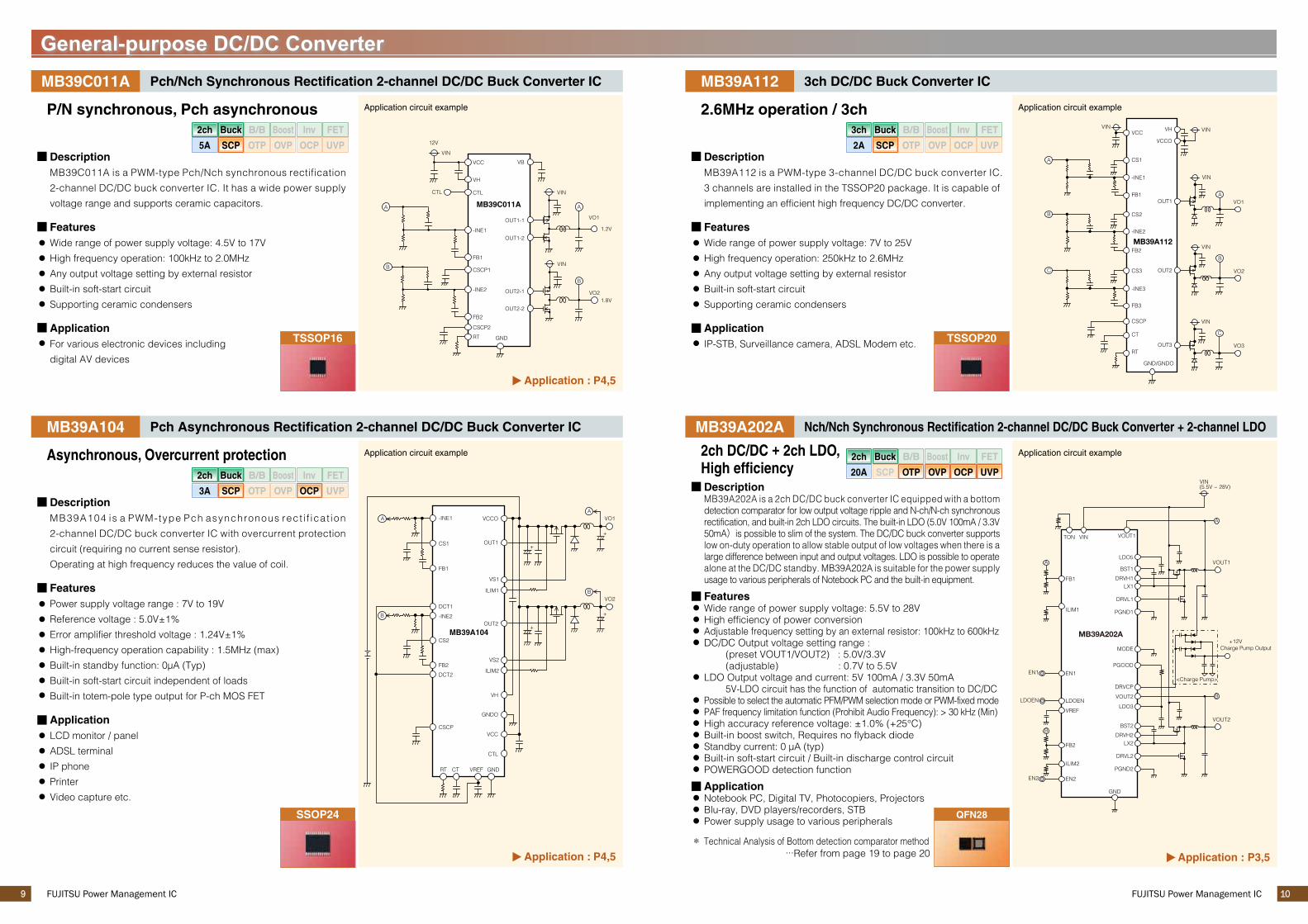
General-purpose DC/DC ConverterMB39C011A Pch/Nch Synchronous Rectification 2-channel DC/DC Buck Converter IC
MB39A104 Pch Asynchronous Rectification 2-channel DC/DC Buck Converter IC
Application circuit example
MB39A112 3ch DC/DC Buck Converter IC
Nch/Nch Synchronous Rectification 2-channel DC/DC Buck Converter + 2-channel LDO
P/N synchronous, Pch asynchronous
DescriptionMB39C011A is a PWM-type Pch/Nch synchronous rectification
2-channel DC/DC buck converter IC. It has a wide power supply
voltage range and supports ceramic capacitors.
FeaturesWide range of power supply voltage: 4.5V to 17V
High frequency operation: 100kHz to 2.0MHz
Any output voltage setting by external resistor
Built-in soft-start circuit
Supporting ceramic condensers
ApplicationFor various electronic devices including
digital AV devices
Application : P4,5
Asynchronous, Overcurrent protection 2ch DC/DC + 2ch LDO,High efficiency
DescriptionMB39A104 is a PWM-type Pch asynchronous rect i f icat ion
2-channel DC/DC buck converter IC with overcurrent protection
circuit (requiring no current sense resistor).
Operating at high frequency reduces the value of coil.
FeaturesPower supply voltage range : 7V to 19V
Reference voltage : 5.0V±1%
Error amplifier threshold voltage : 1.24V±1%
High-frequency operation capability : 1.5MHz (max)
Built-in standby function: 0µA (Typ)
Built-in soft-start circuit independent of loads
Built-in totem-pole type output for P-ch MOS FET
ApplicationLCD monitor / panel
ADSL terminal
IP phone
Printer
Video capture etc.
DescriptionMB39A202A is a 2ch DC/DC buck converter IC equipped with a bottom detection comparator for low output voltage ripple and N-ch/N-ch synchronous rectification, and built-in 2ch LDO circuits. The built-in LDO (5.0V 100mA / 3.3V 50mA)is possible to slim of the system. The DC/DC buck converter supports low on-duty operation to allow stable output of low voltages when there is a large difference between input and output voltages. LDO is possible to operate alone at the DC/DC standby. MB39A202A is suitable for the power supply usage to various peripherals of Notebook PC and the built-in equipment.
FeaturesWide range of power supply voltage: 5.5V to 28VHigh efficiency of power conversionAdjustable frequency setting by an external resistor: 100kHz to 600kHzDC/DC Output voltage setting range : (preset VOUT1/VOUT2) : 5.0V/3.3V (adjustable) : 0.7V to 5.5VLDO Output voltage and current: 5V 100mA / 3.3V 50mA 5V-LDO circuit has the function of automatic transition to DC/DC Possible to select the automatic PFM/PWM selection mode or PWM-fixed modePAF frequency limitation function (Prohibit Audio Frequency): > 30 kHz (Min)High accuracy reference voltage: ±1.0% (+25°C)Built-in boost switch, Requires no flyback diodeStandby current: 0 µA (typ)Built-in soft-start circuit / Built-in discharge control circuitPOWERGOOD detection function
ApplicationNotebook PC, Digital TV, Photocopiers, ProjectorsBlu-ray, DVD players/recorders, STBPower supply usage to various peripherals
Application : P4,5
2.6MHz operation / 3ch
DescriptionMB39A112 is a PWM-type 3-channel DC/DC buck converter IC.
3 channels are installed in the TSSOP20 package. It is capable of
implementing an efficient high frequency DC/DC converter.
FeaturesWide range of power supply voltage: 7V to 25V
High frequency operation: 250kHz to 2.6MHz
Any output voltage setting by external resistor
Built-in soft-start circuit
Supporting ceramic condensers
ApplicationIP-STB, Surveillance camera, ADSL Modem etc.
Application : P3,5
MB39A202A
QFN28
* Technical Analysis of Bottom detection comparator method ...Refer from page 19 to page 20
FUJITSU Power Management IC11 FUJITSU Power Management IC 12
VIN VOUT1.8V
L12.2µH
R2300kΩ
R1294kΩ
C24.7µF
C30.1µF
CTL
VREF
VREFIN
MB39C006AR31MΩ
CTL
VREF
VREFINGND
OUT
POWERGOOD
LXVDD
FSEL
MODER41MΩ
C14.7µF
MB39C007
CTL1
MODE1
VREFIN1
OUT1
XPOR
LX1
DVDD1
CTL2
MODE2
VREF
VREFIN2
VDET
CTLP
DVDD2
DGND1
DGND2
AVDD
AGND
OUT2
LX2
XPOR
VIN
VOUT12.5V
VOUT21.5V
CTL1
CTL2
VREFIN1
VREFIN2
C24.7µF
C14.7µF
L12.2µH
L22.2µH
C54.7µF
R41MΩ
R91MΩ
R101MΩ
C44.7µF
C34.7µF
C60.1µF
C70.1µF
R6300kΩ
R8100kΩ
R7510kΩ
R5352kΩ
R2170kΩ
R11MΩ
R3300kΩ
MB39C015
CTL1
MODE1
VREFIN1
OUT1
XPOR
LX1
DVDD1
CTL2
MODE2
VREF
VREFIN2
VDET
CTLP
DVDD2
DGND1
DGND2
AVDD
AGND
OUT2
LX2
XPOR
VIN
VOUT12.5V
VOUT21.5V
CTL1
CTL2
VREFIN1
VREFIN2
C24.7µF
C14.7µF
L12.2µH
L22.2µH
C54.7µF
R41MΩ
R91MΩ
R101MΩ
C44.7µF
C34.7µF
C60.1µF
C70.1µF
R6300kΩ
R8100kΩ
R7510kΩ
R5352kΩ
R2170kΩ
R11MΩ
R3300kΩ
1ch Buck B/B Boost Inv FET
OTP OVP UVPOCPSCP0.8A
2ch Buck B/B Boost Inv FET
OTP OVP UVPOCPSCP0.8A
1ch Buck B/B Boost Inv FET
OTP OVP UVPOCPSCP0.8A
2ch Buck B/B Boost Inv FET
OTP OVP UVPOCPSCP0.8A
SON10
QFN24
VIN VOUT1.8V
L12.2µH
R2300kΩ
R1294kΩ
C24.7µF
C30.1µF
CTL
VREF
VREFIN
MB39C014R31MΩ
CTL
VREF
VREFINGND
OUT
POWERGOOD
LXVDD
FSEL
MODER41MΩ
C14.7µF
DC/DC Converter with Switching FET
Application circuit example
Application circuit example
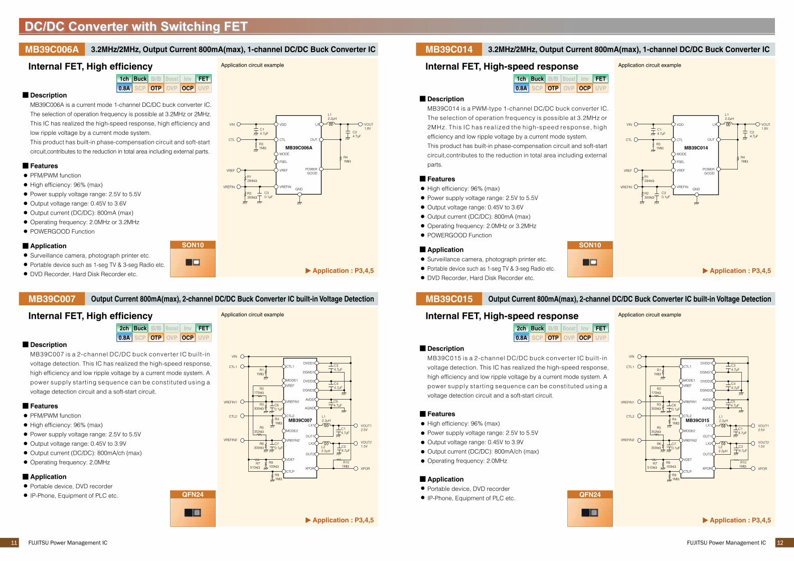
MB39C006A 3.2MHz/2MHz, Output Current 800mA(max), 1-channel DC/DC Buck Converter IC
MB39C007 Output Current 800mA(max), 2-channel DC/DC Buck Converter IC built-in Voltage Detection
Application circuit example
Application circuit example
SON10
QFN24
MB39C014 3.2MHz/2MHz, Output Current 800mA(max), 1-channel DC/DC Buck Converter IC
MB39C015 Output Current 800mA(max), 2-channel DC/DC Buck Converter IC built-in Voltage Detection
Internal FET, High efficiency
DescriptionMB39C006A is a current mode 1-channel DC/DC buck converter IC.
The selection of operation frequency is possible at 3.2MHz or 2MHz.
This IC has realized the high-speed response, high efficiency and
low ripple voltage by a current mode system.
This product has built-in phase-compensation circuit and soft-start
circuit,contributes to the reduction in total area including external parts.
FeaturesPFM/PWM function
High efficiency: 96% (max)
Power supply voltage range: 2.5V to 5.5V
Output voltage range: 0.45V to 3.6V
Output current (DC/DC): 800mA (max)
Operating frequency: 2.0MHz or 3.2MHz
POWERGOOD Function
ApplicationSurveillance camera, photograph printer etc.
Portable device such as 1-seg TV & 3-seg Radio etc.
DVD Recorder, Hard Disk Recorder etc. Application : P3,4,5
Application : P3,4,5 Application : P3,4,5
Application : P3,4,5
DescriptionMB39C007 is a 2-channel DC/DC buck converter IC built- in
voltage detection. This IC has realized the high-speed response,
high efficiency and low ripple voltage by a current mode system. A
power supply start ing sequence can be constituted using a
voltage detection circuit and a soft-start circuit.
FeaturesPFM/PWM function
High efficiency: 96% (max)
Power supply voltage range: 2.5V to 5.5V
Output voltage range: 0.45V to 3.9V
Output current (DC/DC): 800mA/ch (max)
Operating frequency: 2.0MHz
ApplicationPortable device, DVD recorder
IP-Phone, Equipment of PLC etc.
Internal FET, High efficiency
Internal FET, High-speed response
DescriptionMB39C014 is a PWM-type 1-channel DC/DC buck converter IC.
The selection of operation frequency is possible at 3.2MHz or
2MHz. This IC has real ized the high-speed response, high
efficiency and low ripple voltage by a current mode system.
This product has built-in phase-compensation circuit and soft-start
circuit,contributes to the reduction in total area including external
parts.
FeaturesHigh efficiency: 96% (max)
Power supply voltage range: 2.5V to 5.5V
Output voltage range: 0.45V to 3.6V
Output current (DC/DC): 800mA (max)
Operating frequency: 2.0MHz or 3.2MHz
POWERGOOD Function
ApplicationSurveillance camera, photograph printer etc.
Portable device such as 1-seg TV & 3-seg Radio etc.
DVD Recorder, Hard Disk Recorder etc.
Internal FET, High-speed response
DescriptionMB39C015 is a 2-channel DC/DC buck converter IC built- in
voltage detection. This IC has realized the high-speed response,
high efficiency and low ripple voltage by a current mode system. A
power supply start ing sequence can be constituted using a
voltage detection circuit and a soft-start circuit.
FeaturesHigh efficiency: 96% (max)
Power supply voltage range: 2.5V to 5.5V
Output voltage range: 0.45V to 3.9V
Output current (DC/DC): 800mA/ch (max)
Operating frequency: 2.0MHz
ApplicationPortable device, DVD recorder
IP-Phone, Equipment of PLC etc.

FUJITSU Power Management IC13 FUJITSU Power Management IC 14
SON10
MB39C316
DC/DC 3chLDO 4ch
FLASH
SDRAM
SoC
3.3V/650mA
32.768kHz
1.2V/800mA
2.85V/200mA
(1.2V/1.3V)/84mA
2.9V/6.5mA
1.2V/260mA
1.8V/600mA
I2C
Li-ionbattery
VIN=2.7V to 5.5VSystem part
Applicationpart
Crystaloscillator
WL-CSP493.13.10.8(mm)
1ch Buck B/B Boost Inv FET
OTP OVP UVPOCPSCP0.6A EN2
VIN2
VOUT2
POR
GND2 FB
EN1
VIN1
LX
GND1
EN1
C4
C5
C2
C1
L1
R5
R3 C3R6
VO1IO1 ≤ 600 mA
POR
EN2
VO2IO2 ≤ 300 mA
MB39C022
VIN
3ch Buck B/B Boost Inv FET
OTP OVP UVPOCPSCP0.8A
Lineup of General-purpose DC/DC Converter
PFM/PWM, PAF, Bottom detection comparator, N/N synchronousrectification, soft-start circuit, discharge control circuit, overvoltage protection, under-voltage protection, overcurrent protection,over-temperature protection, built-in boot-strap diode
PFM/PWM, PAF, Bottom detection comparator, N/N synchronousrectification, soft-start circuit, discharge control circuit, overvoltage protection, under-voltage protection, overcurrent protection,over-temperature protection, built-in boost-switch, POWERGOOD circuit
MB39A214
General-purpose DC/DC Converter and DC/DC Converter with Switching FET
MB39C022G
MB39C022J
MB39C022L
MB39C022N
1 1 +2.5 to +5.52000
BuckDCDC 0.8 to 4.5
3.3
2.85
1.8
1.2
LDO
Internal
SON10
600
300
Soft-start circuit, timer-latch short-circuit protection
Soft-start circuit, timer-latch short-circuit protection, timer-latch overcurrent protection
PWM, Current mode system, low-consumption current, synchronous rectification, POWERGOOD function,support for the input signal to DAC
PWM, Current mode system,low-consumption current, synchronous rectification, voltage detection function included, support for the input signal to DAC
PFM/PWM, Current mode system, low-consumption current, synchronous rectification, POWERGOOD function,support for the input signal to DAC
PFM/PWM, Current mode system,low-consumption current, synchronous rectification, voltage detection function included, support for the input signal to DAC
Pch asynchronous rectification, individual channel control, soft-start circuit
For various types of power supplies such as LCD backlight, car navigation devices, audio devices, game consoles and portable devices.* : Recommended : Possible with the addition of outside partsPAF=Prohibit Audio Freguency
Suitable for internal power supply in portable devices such as cellular phones, PDA, and in DVD, HDD, etc.
Bottom detection comparator, N/N synchronous rectification, soft-start circuit, discharge control circuit, overvoltage protection, under-voltage protection, overcurrent protection,over-temperature protection, POWERGOOD circuit
Selectable fixed PWM mode or automatic PFM/PWM mode, N/N synchronous rectification, current mode system, overvoltage protection, under-voltage protection, overcurrent control circuit, over-temperature protection, soft-start circuit, soft-stop circuit
Selectable fixed PWM mode or automatic PFM/PWM mode, N/N synchronous rectification, current mode system, overvoltage protection, under-voltage protection, overcurrent control circuit, over-temperature protection, soft-start circuit, soft-stop circuit
Lineup of DC/DC Converter with Switching FET
MB3800 1 - 1000 +1.8 to +15 ±4 SOP8, SSOP8
1 - 600 +4.5 to +25 ±1.5 TSSOP24
1 - 1000 +4.5 to +25 ±1 TSSOP16
2 - 1500 +7 to +19 ±1 SSOP24
2 - 1000 +4.5 to +25 ±1 TSSOP24
2 - 310/620/1000 +6.0 to +28.0 ±0.7 TSSOP24
2 2 100 to 600 +5.5 to +28 ±1 QFN28
2 - 2000 +4.5 to +17 ±1 TSSOP16
3 - 2600 +7 to +25 ±1 TSSOP20
MB39A130A
MB39A135
MB39A104
MB39A136
P/N synchronous rectification (Pch asynchronous rectification), timer-latch short-circuit protection, soft-start circuit, symmetrical-phase mode
MB39C011A
MB39A112
MB39C014 1 2.5 ±4 +2.5 to +5.5 800 0.3 0.2 SON10 Buck2000/3200
(fixed)
MB39C006A 1 2.5 ±4 +2.5 to +5.5 800 0.3 0.2 SON10 Buck2000/3200
(fixed)
MB39C015 2 2.5 ±4 +2.5 to +5.5 800/ch 0.3 0.2 QFN24 Buck2000
(fixed)
MB39C007 2 2.5 ±4 +2.5 to +5.5 800/ch 0.3 0.2 QFN24 Buck2000
(fixed)
DC/DC Converter with Switching FET + LDOMB39C022 Series 1-channel DC/DC Buck Converter IC + 1-channel Low-Noise LDO + POR
System configuration of Mobile Terminals
MB39C316 3-channel DC/DC Converter + 4-channel LDO
Lineup of DC/DC Converter with Switching FET + LDO
MB39C316 3 4 +2.7 to +5.51700 WL-CSP49
Buck
Buck
Buck/BoostCurrent mode system, synchronous rectification,output short-circuit protection, over-temperature protection, overcurrent protection, under voltage lock out protection
DCDC1
DCDC2
DCDC3
LDO1
LDO2
LDO3
1.2
1.825
3.3
2.875
1.225
1.20/1.30
Internal
800
600
650
200
260
6.5
LDO4 2.925 84
Not available
Available
Available
Available
Available
Available
MB39A202A Available
Available
Available
Model
Powersupplyvoltage
V
Referencevoltage
accuracy%
Package
TopologyFET
compatibleRemarks
Switchingfrequency(max)kHz BoostBuck
Number ofchannels
ch
LDOD/D
Model
Powersupplyvoltage
V
Package Topology RemarksSwitchingfrequency
MHz
Number ofchannels
ch(Typ)
VPch MOS
(typ)ΩNch MOS
(typ)Ω
Output current(max)mA
Switching FET
Accuracy%
Output voltage
For Portable Devices with digital circuits and with analog circuits
DescriptionAn optimal IC for power management systems in portable devices with one built-in channel of DC/DC step-down converter for digital circuits and one built-in channel of low-noise LDO for analog circuits. Two power management systems is in a 10-pin package of 3.0mm x 3.0mm.The built-in switching FET enable the construction of a power management system at a low BOM cost. There are four variations of the fixed output voltage in the LDO block.
FeaturesPower supply voltage range: 2.5V to 5.5V Supporting 1-cell Li-ion BatteryFunction of DC/DC circuit: PFM/PWM mode: Improving efficiency under light load Current mode: High-speed load responseOutput voltage/current of DC/DC block: Voltage setting range: 0.8V to 4.5V Current: 600mA (Max.)
Output voltage/current of LDO block: Output voltage (fixed): 3.3V (MB39C022G) 2.85V (MB39C022J) 1.8V (MB39C022L) 1.2V (MB39C022N) Current: 300mA (Max.)Power on Reset (POR)Package: SON-10 3.0mm×3.0mm×0.75mm (lead pitch 0.5mm)
ApplicationPortable applicationsGPS, PNDMP3, PMPPortable TV, USB dongle (CMMB, DVB-T, DMB-T)SMART-PHONE, etc.
Application : P3,5
Application : P3,5
Supporting 1-cell Li-ion BatteryDescriptionMB39C316 is a power management IC equipped with 3ch DC/DC converter and the 4ch linear regulator (LDO). MB39C316 operate in the range of power supply voltage with 1-cell Li-ion power by 1ch buck boost DC/DC converter of high efficiency, and has 4ch LDO which is suitable to supply voltage for mobile terminals.
FeaturesPower supply voltage range : 2.7V to 5.5VSequence control: On/Off control of power supply voltageI2C bus interface: Control and notice of internal conditionRTC: Possible to output the 32.768kHz clock by connecting crystal oscillator
ApplicationPortable Products such as PDAMobile WiMAX terminals *:MB39C316 consist of the chipset for Mobile WiMAX terminals with MB86K22 (BaseBand) and MB86K52 (RF).
Model
Powersupplyvoltage
V
Package RemarksTopology
Switchingfrequency
kHz
Number ofchannels
ch
Output features
Pin name Output voltageV
Output current(max)mA
FETDCDC LDO
PFM/PWM, current mode system, synchronous rectification, short-circuit protection, overcurrent protection, over-temperature protection, under voltage lock out protection, POR(Power on Reset)
Product Analysis of this product ...Refer from page 21 to page 22
*
MB39C022(Common)
Application circuit example
MemoMemoMemo

MemoMemoMemo
FUJITSU Power Management IC15 FUJITSU Power Management IC 16
TSSOP28
(Exposed PAD)
DDR
TCON
Buck DC/DC 3.3V
Gat
e D
riverCharge Pump
32V
Source Driver
Charge Pump
-5V
Boost DC/DC
17.7V
LCD PanelMB39C313AMB39C313B
DC/DC converter
4ch Buck B/B Boost Inv FET
OTP OVP UVPOCPSCP1.5A
6ch Buck B/B Boost Inv FET
OTP OVP UVPOCPSCP0.6A
VO1VIN
VCC
VO2
VO3
VO4
VO5
VO6
MB39A123
-INE1
-INE2
-INE3
-INA
-OUTA
-INE4
-INE5
-INE6
OUT1-1OUT1-2
OUT2
OUT3
OUT4
OUT5
OUT6GND
WL-CSP202.15×1.94×0.625(mm)
1ch Buck B/B Boost Inv FET
OTP OVP UVPOCPSCP2A
CIN COUT
2.2 µF (1608)10 µF (1608) VDD
VCC
ENILIMSEL
SWOUT
0.5 µH
L1
VSEL
VSELSW
FB
GND
DGND
VOUT
R3 R2
R1XPS
2.5 V~4.8 VVBATT
MB39C326
Internal
System configuration of LCD panel
DC/DC Converter for LCD Panels
Lineup of DC/DC Converter for LCD Panels
MB39C313AMB39C313B
4TSSOP28
(Exposed PAD)
1.213
1.146
0±36mV
1.213
Vlogic
Vs
VGL
VGH
1.5
0.9
2.1
1.8 to 3.3
18.1(max)
1.5
1.5 *1
100mA
100mA
InternalBuck DC/DC
Boost DC/DC
Invert charge pump
Boost charge pump
500/750 +8 to +14
soft-start circuit, sequence comparator, short-circuit protection, overvoltage protection, over-temperature protection, over current protection (Vlogic, Vs):
Vs Detection value: 3.5A(MB39C313A)4.6A(MB39C313B)
*: Conditions: Input voltage=12V, Output voltage=15V
Application : P5
Application : P5 VIN=8V to 14V
DC/DC + Charge pump
DescriptionMB39C313A/MB39C313B is a 4ch system power management IC. It consists of 2ch DC/DC converter and 2ch charge pump type DC/DC converter.
FeaturesPower supply voltage range: 8V to 14VStructure: Vlogic/Vs: voltage mode DC/DC converter included switching FET VGL/VGH: charge pump with output voltage feedbackBuilt-in soft-start circuit independent of loadsExcellent line regulation with the feed-forward method (Vlogic, Vs)Built-in phase compensator parts (Vlogic; buck DC/DC)Built-in sequence comparator for risingFrequency setting by input pin: 500kHz / 750kHzOver current protection (Vlogic, Vs): Vs Detection value: 3.5A (MB39C313A)
4.6A (MB39C313B)
ApplicationLarge size LCD panel
Model Error amplifier threshold voltage
V
Pinname Structure
PackageOutputvoltage
VFET
RemarksSwitchingfrequency(fixed)MHz
Number ofchannels
ch
Powersupplyvoltage
V
Outputcurrent
AAccuracy
%
Output features
MB39A123 6 +1.7 to +11 ±1 LQFP48 AvailableSynchronous rectification, individual channel control, soft-start function, support for external input short-circuit detection
2000
MB39A123 6ch DC/DC Converter IC with Synchronous Rectification
System power management IC Supporting 2-cell Li-ion Battery
DescriptionMB39A123 is a 6-channel DC/DC converter IC using pulse width modulation (PWM), and it is suitable for boost conversion, buck conversion, and boost/buck conversion.
FeaturesPower supply voltage range: 1.7V to 11VSupports for buck converter with synchronous rectificationNegative voltage output (Inverting amplifier)Low voltage start-up: 1.7VSupport for the output voltage of 1.0VSupport for control and soft-start of each channelOscillation frequency range: 200kHz to 2.0MHz
ModelPower supply
voltageV
Referencevoltage accuracy
%Package FET
compatible RemarksSwitching
frequency(max)kHz
Number ofchannels
ch
Topology
Buck BoostBuck/Boost
Inverter
For portable devices such as DSC and DVC. * : Recommended
Power Supply for RF Power AmplifierPower Supply for RF Power Amplifier
Application circuit example
MB39C326 6MHz Synchronous Buck-Boost DC/DC Converter IC
Lineup of DC/DC Converter IC for System Power Supply
Application circuit example
LQFP48
Power Supply for RF Power Amplifier
DC/DC Converter IC for System Power Supply
6MHz Buck-Boost, Reduced board spaceDescriptionMB39C326 is a high efficiency, low noise synchronous, 6MHz buck-boost DC/DC converter designed for powering the radio frequency power amplifiers (RFPA) in mobile handsets or other mobile applications with single-cell Li-ion battery. MB39C326 DC/DC convertor switches at 6MHz compare to conventional DC/DC converters that have switching frequencies between 2 to 3MHz, allowing smaller inductor to be use and expect to reduce the overall board space of the power management circuits by half. Its buck boost operation switches automatically to extend the operating voltage of lithium battery while providing stable power supply to the power amplifier.
FeaturesHigh efficiencyPower Supply voltage range : 2.5V to 4.8VAdjustable output voltage range : 0.4V to 4.5VInput current limit value : 2000mA6MHz PWM operation allows 0.5 µH small form inductorLess than 20 µs step response for 3GAutomatic Transition between buck mode and boost modeSelectable output voltage with external resistor
ApplicationMobile phones, Smart phones, e-Books, PDAsRF-PAs powered by 1cell Li-ion battery RF-PC cards
MB39C313A/MB39C313B 4-channel DC/DC Converter IC for LCD Panel
ApplicationDigital still cameraDigital video cameraSurveillance camera
ModelNumber ofchannels
ch
Outout voltageSwitchingfrequency(max)kHz (Typ)
V
Inputcurrent
limit valuemA
FET
MB39C326 1+0.4 to+4.5 ±3 +2.5 to +4.8 800 2000 WL-CSP206000
Accuracy%
Powersupplyvoltage
V
Outputcurrent(max)mA
Package Topology Remarks
Buck/Boost
PFM/PWM, synchronous rectification, over-temperature protection,overcurrent protection, under voltage lock out protection,Automatic Transition between buck mode and boost mode,Selectable output voltage with external resistor

FUJITSU Power Management IC17 FUJITSU Power Management IC 18
Sel
ecto
r
DC/DC CPU
DC/DC Display
DC/DC I/O Controller
DC/DC Memory
DC/DC Application
MB39A134
Charger
AC Adapter
Battery
KBC+PMU
Sel
ecto
r
DC/DC CPU
DC/DC Display
DC/DC I/O Controller
DC/DC Memory
DC/DC Application
MB39A132
Charger
AC Adapter
Battery
KBC+PMU
1ch Buck B/B Boost Inv FET
OTP OVP UVPOCPSCP4A
1ch Buck B/B Boost Inv FET
OTP OVP UVPOCPSCP4A
CK1
GND
CK2
INH
VCC
VCC
MPU2
GND
CK
RESET VCC
MPU1
GND
CK
CTW CTP
MB3793
CTW
CTP
RESET
RESET
VCC
Charge ControlMB39A134 DC/DC Converter IC for Charging Li-ion Battery
MB39A132A DC/DC Converter IC for Charging Li-ion Battery
Lineup of Charge Control
System configuration of Notebook PC
System configuration of Notebook PC
TSSOP24
Buck AvailableTSSOP24 MB39A134 2000 +8 to +254.2 or 4.1/cell, Optional
±0.5 ±0.7*12 to 4 cells, Charging voltage can be set without externally attached resistor,charging current can be set without externally attached resistor,dynamically controlled charging, ACOK function included, soft-start circuit
QFN32MB39A132A Buck Available2000 +8 to +254.0 or 4.2 or 4.35/cell, Optional
±0.5 ±0.5*22 to 4 cells, Charging voltage can be set without externally attached resistor, charging current can be set without externally attached resistor, dynamically controlled charging, ACOK function included, soft-start circuit
QFN32
Application : P3
Preset output-voltage, CVM
DescriptionMB39A134 is a DC/DC converter IC for charging Li-ion battery, which is suitable for buck conversion, and uses pulse width modulation (PWM) for controlling the output voltage and current independently.
FeaturesPower supply voltage range: 8V to 25VSupport 2, 3 and 4 Cell battery packTopology: Pch/Diode , asynchronous rectificationAC adapter voltage detection function (ACOK terminal)Output voltage setting accuracy: ±0.7% (Ta=-10°C to +85°C)Charging voltage can be set without externally attached resistorCharging current can be set without externally attached resistorHigh accuracy current detection amplifier (±1%)
(At input voltage difference 100mV)
ApplicationCharging device in products such as Notebook PC
Application : P3
Nch/Nch synchronous, Preset output-voltage
DescriptionMB39A132A is a DC/DC converter IC for charging Li-ion battery, which is suitable for buck conversion, and uses pulse width modulation (PWM) for controlling the output voltage and current independently.
FeaturesPower supply voltage range: 8V to 25VSupport 2, 3 and 4 Cell battery packTopology: Nch/Nch , synchronous rectificationAC adapter voltage detection function (ACOK terminal)Output voltage setting accuracy: ±0.5% (Ta=+25°C to +85°C)Charging voltage can be set without externally attached resistorCharging current can be set without externally attached resistorHigh accuracy current detection amplifier (±1%)
(At input voltage difference 100mV)
ApplicationCharging device in products such as Notebook PC
ModelPower supply
voltageV
PackageAccuracy %
TopologyFET
compatible RemarksSwitchingfrequency(max)kHz
Outputvoltage
V Ta=25°C Ta=-30 to 85°C
*1: Ta=-10 to +85°C*2: Ta=25 to +85°C
For portable devices using Li-ion battery, such as Notebook PC, Netbook PC etc.
Technical Analysis of this product ...Refer from page 23 to page 24
*
Technical Analysis of this product ...Refer from page 23 to page 24
*
MB3759
MB3769A
MB3841
MB3842MB3845
Lineup of AC/DC Converter
Lineup of Power Management Switches
Power Voltage Monitoring Applications MB3793 Power voltage monitoring IC with dual-system watchdog timer
Lineup of Power Voltage Monitoring Application
System configuration
SSOP8SOP8SOP8
Used in power supplies for various applications, including automobiles, hot water systems, copiers, VCRs, hard-disk drives, general OA equipment, measuring instruments, and pachinko parlor pinball machines.
MB3771 Power supply voltage monitor SOP8
MB3773 MB3771+ watchdog timer SOP8
MB3793-XXPower supply voltage monitorwith dual-system watchdog timer
SOP8, SSOP8
Application : P3
DescriptionMB3793 is a power voltage monitor ing IC with dual-system watchdog timer. A reset signal is output at transient power cut-off or power fall. When the power resumes, the IC outputs a power-on reset signal to MPU to monitor power voltage. Using this IC in an MCU system can provide such system with a fail-safe function.
FeaturesDetection voltage: 4.5V/4.2V/3.7V/3.4V/3.0V/2.8V/2.7V 7typePrecise detection of power voltage fall: ±2.5%Detection voltage with hysteresisInternal dual-input watchdog timerWatchdog-timer halt function (by inhibition pin)Independently-set watchdog and reset times
ApplicationArcade AmusementPBX and base stationsVending machines etc.
Built-in Watchdog timer
FunctionDetection voltage
V
Power supplyvoltage
VPackage RemarksModel
+3.5 to +18
+3.5 to +16
6(max)
4(max)
Model Package RemarksConsumption current
(Sw OFF)A
On resistanceΩ
Drive current(max)
A
Switching voltage(max)
V
0 0.045 2 5.5 SOP8 1 channel USB
0 0.1 0.6 5.5 SSOP202 channel USBSwitching changeover logic differs for the MB3842 and MB3845.
Modeloscillationfrequency(max)kHz
Power supplyvoltage
V
Maximum output currentmA
Package Remarks
300 +7 to +32 200 SOP16 TL494 pin-compatible
700 +12 to +18 DC 100, peak 600 SOP16 Power MOS FET
Voltages other than 4.2V optionally available
Voltages other than 4.2V optionally available
4.5(-45), 4.2(-42), 3.7(-37A), 3.4(-34A), 3.0(-30A)
2.7(-27A), 2.8(-28A) *: "( )" corresponds to "-XX" of a product name.

FUJITSU Power Management IC19 FUJITSU Power Management IC 20
Figure 1 Block Diagram for the Bottom Detection Comparator Method and Control Theory
Figure 2 Load Fluctuation Waveform for the Bottom Detection Comparator Method
MB39A214 External View
Evaluation Board MB39A214
Application Example
Table of Bottom detection comparator method DC/DC converter IC
Addition ofa proprietarycircuit
FBINTREF
VOUT
VOUT
VIN
VIN
ILXLX
Vref
<Error Comp.>
tONgenerator
SlopeDetector
BiasReg.
DriveLogic
Bias
DRVH
Hi-sideDrive
Slope DRVL
Lo-sideDrive
tON
RS-FFRS out
R
S
QError out
Ripple not required for FB
FB
tOFF
tON
INTREF
RS out
Smallripples
5A/div
10V/div
100mV/div
4.0us/div
②②
④④
①① ③③
Load current : 0A 5ALoad current : 0A 5A
LX waveformLX waveform
Output voltage : 1.2VOutput voltage : 1.2V
Stationary state: Stable load current and output voltage
Load fluctuation: Rapid increase in load current
Output voltage fluctuation: Undershooting of output voltage due to rapid load fluctuation
Switching control: Output voltage is recovered by changing the off period and implementing switching control in succession depending on the output voltage fluctuation
1.8V/1.5V12V
1.0V
3.3V
AC/DC DDR2/3
CoreSystem LSII/O
Flashmemory
MB39A2142ch DC/DC
Ultra-rapid load transition response!
Best for System LSI Core and DDR2/3 etc.
*The DC/DC part of MB39A202A(refer to page 10) adopts "Bottom detection comparator method for the low output voltage ripple" in this page.
INTREF is the voltage that the slope was added to a reference voltage (Vref) by the new original circuit. When the value of INTREF becomes equal to FB, the high-side FET is turned on.
MB39A214
4.4×6.5×1.2mm(0.5mm Lead Pitch )
Noteworthy Non-linear Hysteresis Control Method As a DC/DC Converter Control Method
"Bottom detection comparator method" is the best method for the power supply to the Core of system LSI with the severe demand
of the power-supply voltage accuracy, to the memory, to the power-supply specification with the large I/O voltage difference.
MB39A214 achieved a low output ripple operation by adding our improved new circuit to a past bottom detection comparator method.
Although the conventional mainstream DC/DC converter control methods were voltage control or current control, recently the non-linear hysteresis control method attracts attention along with the lowering the voltage of the power-supply voltage of system LSI. Since 2005, FUJITSU has shipped more than 100 million DC/DC converter ICs that adopt the bottom detection comparator method (a type of hysteresis control method), mainly to the commercial market.The reason why this method attracts attention is an excellent point in "High-speed load transition response characteristic" and "Low on-duty operation with stability". Moreover, the power supply design is easy.
Outline of Bottom detection comparator method
The bottom detection comparator method compares with the comparator of a feedback voltage and a reference voltage always, and keeps the output voltage by off-time control and the fixed on-time.Therefore, when the output voltage changes by a rapid change in the load, this method rapidly stabilizes the output voltage by controlling the off-time and changing the switching frequency. (Refer to Fig.2)This method is best for the system that the low voltage power supply is especially necessary, because the voltage stability is more excellent than the voltage control and the current control method using a conventional error amplifier.In addition, this method can reduce the output capacitor for smoothness, because the voltage stability is excellent. This point contributes to the part cost reduction in the entire set.
Feature 1: High-speed load transition response characteristic
In the voltage control and the current control method, the phase compensation circuit is necessary to prevent the oscillation of the DC/DC converter output. This circuit is a circuit to adjust the phase delay of a feedback system and the gain of the error amplifier.The bottom detection comparator method has little phase delay for feedback-loop-system. This method uses a comparator without an error amplifier, it therefore requires no phase compensation circuit.Therefore, it is possible to greatly shorten the period of power supply design, without preparing a special measurement environment and without requirement to adjust the circuit at the power supply design.
Feature 2: No phase compensation circuit required
The bottom detection comparator method does switching control by fixing the on-time and by controlling off-time.It is therefore possible to supply stable output voltage without becoming unstable, even under conditions of large input-output voltage difference.Direct conversion is easy to the low voltage power supply from the first power supply. Therefore, the energy-saving effect by the decrease of the conversion loss can be expected compared with the case to use the second or third power supplies.
Feature 3: For low on-duty (Secure on-time switching control)
Specification Item
Topology
External FET
Number of output channels
Maximum Ratings
Power supply voltage
Output voltage
Reference voltage and accuracy
Applicable output condenser
Switching frequency
Startup / Shutdown
Package
Synchronous Rectification Buck Converter
Nch/Nch
Aluminum Solid Capacitors with Organic Semiconductive Electrolyte
Conductive Polymer
MB39A214
2-channel
30V
6.0V to 28V
0.7V to 5.3V
Setting by an external resistor
0.7V±0.7%
310kHz/620kHz/1MHz
selected
TSSOP-24
4.4×6.5×1.2mm
(0.5mm Lead Pitch)
Under Voltage Lock Out Protection
Over Current Protection
Over Voltage Protection
Under Voltage Protection
Over Temperature Protection
ProtectionFunction
MB39A214(2-channel) ... Refer to page 7
Soft-Start /
Internal FET for Discharge

FUJITSU Power Management IC21 FUJITSU Power Management IC 22
Photo 2 Evaluation Board
Figure 1 Block Diagram
Figure 2 Application Example (CMMB, DVB-T, DMB-T)
Figure 3 Application Example (USB-SATA Bridge)
Table 1 Output Settings and Power Supply Rejection Ratio (PSRR) of the LDO block
Table 2 Function Control by EN1 and EN2 Pins
Photo 1 External View
CMMB=China Multimedia Mobile BroadcastingDVB-T=Digital Video Broadcasting - TerrestrialDMB-T=Digital Multimedia Broadcasting - Terrestrial
PDM : Pulse Density Modulation
CurrentLimit
PFMPWMLogic
Control
ICOMP
FB
POR
6
4POR
ErrorAmplifier
DRV
OSC
VREF
OCP
OTP
UVLO
9
LEVELCONV.
7
1
enb1 (H: CH1 ON)
enb2 (H: CH2 ON)
EN1
EN2
VIN or VO1
VIN1
LX
GND1
VIN2
VOUT2
GND2
<<CH1 Buck DC/DC>>
<<CH2: LDO>>
IO2 (300 mA Max)VO2
IO1 (600 mA Max)VO1 (0.8 V to 4.5 V)
VIN(2.5 V to 5.5 V)
<<10 PIN>>
POR
3.3 V: MB39C022G2.85 V: MB39C022J1.8 V: MB39C022L1.2 V: MB39C022N
ErrorAmplifier
10
2
5
8
3
MB39C022G
Functionbutton
LED Quartzoscillator Flash
ROMTR
GPIO
3.3V
5V
1.2V
I/Oport
2.5-inchSATA HDD
I/Oport
AnalogVDD
DigitalVDD
I2C
USBconnector
USB2.0
USB2.0(3.0)bridge IC
USB3.0
MB39C022L
1.2V1.8V
CMMBProcessor
LCD
PDM
SD/MMCBB
Memory
RF
An optimal IC for power management systems in portable devices with one built-in channel of DC/DC step-down converter
for digital circuits and one built-in channel of low-noise LDO for analog circuits. It can also be used in products adopting one
cell of Li-ion battery as the power supply. Two power management systems in a 3.0mm×3.0mm, 10-pin package and the
built-in switching FET enable the construction of a power management system at a low BOM cost. There are four versions
of the fixed output voltage in the LDO block.
The MB39C022 Series are optimal power management ICs for the construction of systems for ARM architecture-based system ICs, GPSs, and portable TVs.Low-noise LDO is demanded for power supplies for RF, PLL, and analog functions. This product is a 2-channel power management IC combining a DC/DC converter and a low-noise LDO. It is useful in electronic devices with mixed analog and digital components.
PFM/PWM control circuit (CH1)The frequency (2.0MHz) set up by the built-in oscillator (square wave oscillating circuit) is used to enable synchronous rectification operation of the built-in P channel MOS FET and N channel MOS FET. PFM operation is executed under light loads.
Iout comparator circuitThis circuit detects the current flowing from the built-in P channel MOS FET to the external inductor (ILX). It compares VIDET obtained by I-V conversion of the ILX peak current and the Error Amp. output to turn OFF the built-in P channel MOS FET through the PFM/PWM logic Control circuit.
Error Amp.(CH1) phase compensation circuitThis circuit compares the VREF reference voltage and the output voltage. The phase compensation circuit of this product is realized by externally attaching a feedback resistor and a capacitor for phase compensation to the FB terminal.
LDO circuit (CH2)The built-in low-noise LDO can output currents up to 300mA. A capacitor is required on the VOUT2 pin for stability.Table 1 presents the output settings and power supply rejection ratio (PSRR) of the LDO block of this product.
Power on Reset (POR) circuitThis circuit monitors the VO1 terminal voltage (CH1 output voltage) via the FB terminal. The POR pin has open drain output. It is normally used in pull-up with an external resistor. While the POR pin reaches H level when VO1 reaches the set output voltage, it is set to L level when the output voltage drops due to over current and so forth.
VREF circuitIt generates a highly precise reference voltage using a BGR (band-gap reference) circuit.
Protection circuit The over-temperature protection circuit (OTP) stops the entire output operation at CH1 and CH2 when the junction temperature reaches +135°C. It restores CH1 and CH2 to normal operation when the junction temperature drops to +110°C. Since the PFM/PWM control circuit adopts the current mode architecture for its control method, the current peak value is constantly monitored and controlled.
Control circuitTable 2 presents the function control by EN1 and EN2 pins.Figure 1 presents the block diagram for this product.
We offer an evaluation board (Photo 2) to simplify the single unit evaluation of this product.
We plan to successively introduce product versions that offer fixed output voltage of the LDO block in the future. We will continue development to meet our customer needs, aiming to address further miniaturization and cost reduction.
Figures 2 and 3 present application examples. This product is optimal for the following applications: - Portable applications - GPS, PND - MP3, PMP - Portable TV, USB dongle (CMMB, DVB-T, DMB-T) - SMART-PHONE, etc.
Product nameOutput voltage setting
in LDO blockPSRR (typical)
MB39C022G 3.3V -70dB
MB39C022J 2.85V -65dB
MB39C022L 1.8V -60dB
MB39C022N 1.2V -55dB
EN1 EN2 CH1 and POR CH2 VREF, UVLO, OTP
L L OFF OFF OFF
H L ON OFF ON
L H OFF ON ON
H H ON ON ON
Input voltage range: 2.5V to 5.5VOutput voltage/current
- DC/DC block (CH1): Voltage setting range: 0.8V to 4.5VCurrent: 600mA (Max.)
- LDO block (CH2): Output voltage (fixed):
3.3V, 2.85V, 1.8V and 1.2VCurrent: 300mA (Max.)
- The DC/DC circuit adopts the PFM/PWM mode to improve efficiency under light load. The current mode architecture is also adopted to achieve high-speed load response.
- The LDO circuit is optimal for power supplies of analog circuits such as RF as it satisfies the low-noise requirement.
- The built-in Power on Reset (POR) function enables the construction of the power startup sequence without signals from an MCU.
Rich protective functionsShort-circuit protection (SCP), over-current protection (OCP), over-temperature protection (OTP), and under voltage lock out protection (UVLO) are provided.Package: SON-10 (Photo 1)Adoption of the SON package contributes to the reduction in the board area of power management circuit.3.0mm×3.0mm×0.75mm (lead pitch 0.5mm)
Product Features
Introduction Functions
Applications
Evaluation Board
Future Development
Power Management IC for Portable Devices 1-Channel DC/DC Converter + 1-Channel Low-Noise LDO + PORMB39C022G / MB39C022J / MB39C022L / MB39C022N
FUJITSU Power Management IC23 FUJITSU Power Management IC 24
Charging voltageConstant voltage
Constant current
Stop ChargingCharging current
MB39A132A
AC adapter
VCC VB
CB
OUT1
OUT2
Nch
Nch
GND
LX
MB39A134
AC adapter
VCC
OUT Pch
Di
GND
VH
Charging voltage Vo (V)
VIN=19V, Io=3A, Ta=+25°C
Con
vers
ion
effic
ienc
y (%
)
0 2 4 6 8 10 12 14 16 18
100
98
96
94
92
90
88
86
84
82
80
MB39A132A
MB39A134
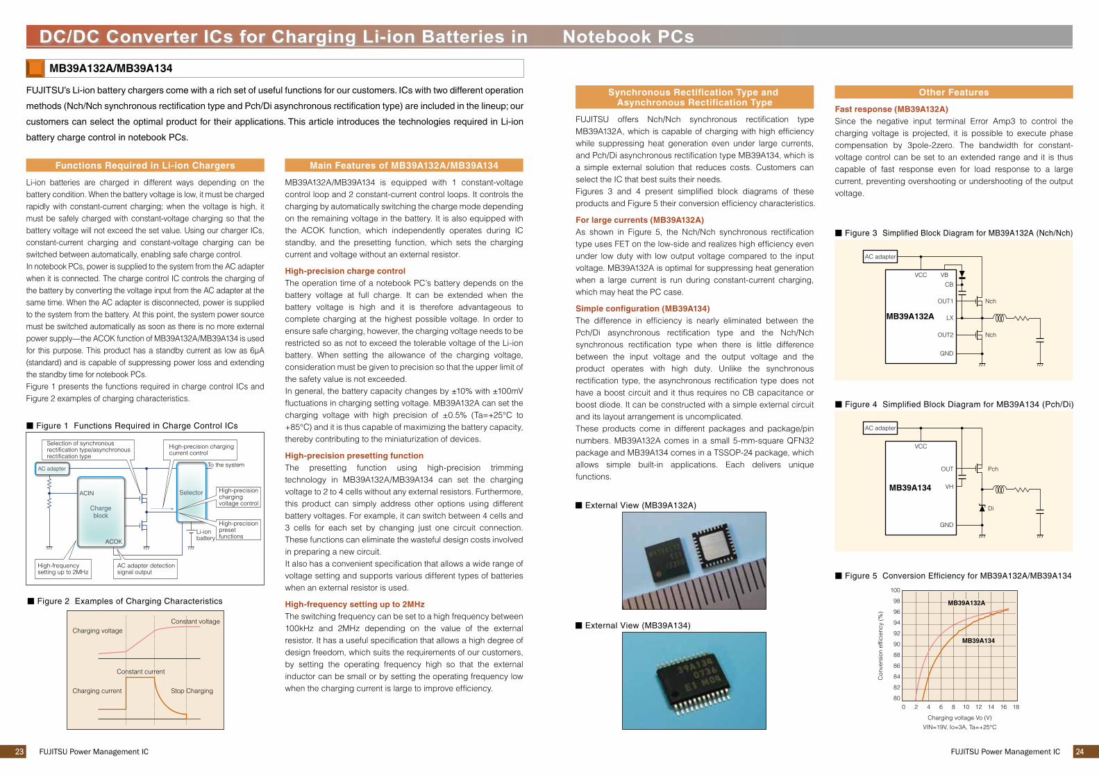
Li-ion batteries are charged in different ways depending on the battery condition. When the battery voltage is low, it must be charged rapidly with constant-current charging; when the voltage is high, it must be safely charged with constant-voltage charging so that the battery voltage will not exceed the set value. Using our charger ICs, constant-current charging and constant-voltage charging can be switched between automatically, enabling safe charge control.In notebook PCs, power is supplied to the system from the AC adapter when it is connected. The charge control IC controls the charging of the battery by converting the voltage input from the AC adapter at the same time. When the AC adapter is disconnected, power is supplied to the system from the battery. At this point, the system power source must be switched automatically as soon as there is no more external power supply—the ACOK function of MB39A132A/MB39A134 is used for this purpose. This product has a standby current as low as 6µA (standard) and is capable of suppressing power loss and extending the standby time for notebook PCs.Figure 1 presents the functions required in charge control ICs and Figure 2 examples of charging characteristics.
Functions Required in Li-ion Chargers
MB39A132A/MB39A134 is equipped with 1 constant-voltage control loop and 2 constant-current control loops. It controls the charging by automatically switching the charge mode depending on the remaining voltage in the battery. It is also equipped with the ACOK function, which independently operates during IC standby, and the presetting function, which sets the charging current and voltage without an external resistor.
High-precision charge controlThe operation time of a notebook PC’s battery depends on the battery voltage at full charge. It can be extended when the battery voltage is high and it is therefore advantageous to complete charging at the highest possible voltage. In order to ensure safe charging, however, the charging voltage needs to be restricted so as not to exceed the tolerable voltage of the Li-ion battery. When setting the allowance of the charging voltage, consideration must be given to precision so that the upper limit of the safety value is not exceeded.In general, the battery capacity changes by ±10% with ±100mV fluctuations in charging setting voltage. MB39A132A can set the charging voltage with high precision of ±0.5% (Ta=+25°C to +85°C) and it is thus capable of maximizing the battery capacity, thereby contributing to the miniaturization of devices.
High-precision presetting functionThe presetting function using high-precision trimming technology in MB39A132A/MB39A134 can set the charging voltage to 2 to 4 cells without any external resistors. Furthermore, this product can simply address other options using different battery voltages. For example, it can switch between 4 cells and 3 cells for each set by changing just one circuit connection. These functions can eliminate the wasteful design costs involved in preparing a new circuit.It also has a convenient specification that allows a wide range of voltage setting and supports various different types of batteries when an external resistor is used.
High-frequency setting up to 2MHzThe switching frequency can be set to a high frequency between 100kHz and 2MHz depending on the value of the external resistor. It has a useful specification that allows a high degree of design freedom, which suits the requirements of our customers, by setting the operating frequency high so that the external inductor can be small or by setting the operating frequency low when the charging current is large to improve efficiency.
Main Features of MB39A132A/MB39A134
FUJITSU offers Nch/Nch synchronous rectification type MB39A132A, which is capable of charging with high efficiency while suppressing heat generation even under large currents, and Pch/Di asynchronous rectification type MB39A134, which is a simple external solution that reduces costs. Customers can select the IC that best suits their needs.Figures 3 and 4 present simplified block diagrams of these products and Figure 5 their conversion efficiency characteristics.
For large currents (MB39A132A)As shown in Figure 5, the Nch/Nch synchronous rectification type uses FET on the low-side and realizes high efficiency even under low duty with low output voltage compared to the input voltage. MB39A132A is optimal for suppressing heat generation when a large current is run during constant-current charging, which may heat the PC case.
Simple configuration (MB39A134)The difference in efficiency is nearly eliminated between the Pch/Di asynchronous rectification type and the Nch/Nch synchronous rectification type when there is little difference between the input voltage and the output voltage and the product operates with high duty. Unlike the synchronous rectification type, the asynchronous rectification type does not have a boost circuit and it thus requires no CB capacitance or boost diode. It can be constructed with a simple external circuit and its layout arrangement is uncomplicated.These products come in different packages and package/pin numbers. MB39A132A comes in a small 5-mm-square QFN32 package and MB39A134 comes in a TSSOP-24 package, which allows simple built-in applications. Each delivers unique functions.
Synchronous Rectification Type and Asynchronous Rectification Type
Fast response (MB39A132A)Since the negative input terminal Error Amp3 to control the charging voltage is projected, it is possible to execute phase compensation by 3pole-2zero. The bandwidth for constant- voltage control can be set to an extended range and it is thus capable of fast response even for load response to a large current, preventing overshooting or undershooting of the output voltage.
Other Features
To the system
Li-ionbattery
Selection of synchronousrectification type/asynchronousrectification type
High-precision chargingcurrent control
AC adapter detectionsignal output
High-frequencysetting up to 2MHz
Chargeblock
Selector
AC adapter
ACOK
ACIN High-precisioncharging voltage control
High-precisionpreset functions
FUJITSU’s Li-ion battery chargers come with a rich set of useful functions for our customers. ICs with two different operation
methods (Nch/Nch synchronous rectification type and Pch/Di asynchronous rectification type) are included in the lineup; our
customers can select the optimal product for their applications. This article introduces the technologies required in Li-ion
battery charge control in notebook PCs.
DC/DC Converter ICs for Charging Li-ion Batteries in Notebook PCsMB39A132A/MB39A134
Figure 1 Functions Required in Charge Control ICs
Figure 2 Examples of Charging Characteristics
Figure 3 Simplified Block Diagram for MB39A132A (Nch/Nch)
Figure 4 Simplified Block Diagram for MB39A134 (Pch/Di)
External View (MB39A134)
External View (MB39A132A)
Figure 5 Conversion Efficiency for MB39A132A/MB39A134

FUJITSU Power Management IC25 26FUJITSU Power Management IC
Fujitsu Semiconductor provides evaluation boards for you to evaluate our semiconductor devices.
You can search our products at the following homepage.URL : http://www.fujitsu.com/global/services/microelectronics/
The details shown above may change without notice. Please contact our sales division for inquiries.
Example: MB39C015 evaluation board Example: MB39C015 connection diagram
For detailed electric properties and operating conditions, refer to the data sheet of each product.
ASSPASSPPower Management ICsPower Management ICs
Package Lineup
RoHS Compliance Information
Package Evaluation Board
Search of Product and Document
0.65mm 0.65mm4.406.501.45mm 5.67.751.45mm0.80mm4.23.51.45mm
SOP Series
SSOP Series
0.65mm4.409.701.20mm
0.50mm3.003.000.75mm
SON Series
0.50mm7.007.001.70mm
LQFP Series
0.4mm4.04.00.8mm0.50mm4.004.000.85mm
QFN Series
0.50mm5.005.000.85mm
Lead (Pb) Free Version Fujitsu LSI products are compliant with RoHS Directive, and observe the standards of lead, cadmium, mercury, hexavalent chromium, polybrominated biphenyls (PBB), and polybrominated diphenyl ethers (PBDE)
An RoHS-compliant product is indicated by trailing characters "E1" in its part number.
Applications
After the list is displayed, you can choose your desired products.
It can search from the Application.
IC Lineup of DC/DC ConverterData sheets
Catalog of Power Management ICs
TSSOP28
Body Size Lead Pitch
SOP8
SSOP8
TSSOP16
SOP8 SOP16
SSOP20 SSOP24
TSSOP24
LQFP48SON10
Body Size Lead Pitch
Body Size Lead Pitch
Body Size Lead Pitch
Body Size Lead Pitch Body Size Lead Pitch
Body Size Lead Pitch Body Size Lead Pitch
Body Size Lead Pitch
Body Size Lead Pitch
Body Size Lead Pitch
Body Size Lead Pitch
0.50mm
TSSOP20
QFN28QFN24
Body Size Lead PitchBody Size Lead Pitch
QFN32
Body Size Lead Pitch
1.27mm 1.27mm 1.27mm3.95.051.75mm 5.36.352.25mm 5.310.152.25mm
0.65mm4.405.001.10mm 0.65mm 0.50mm4.406.501.10mm 4.406.501.20mm
TSSOP Series

FUJITSU Power Management IC27 FUJITSU Power Management IC 28
Fujitsu Semiconductor (Shanghai) Co., Ltd. (FSS)Shanghai
Fujitsu Semiconductor Limited (FSL)Yokohama
Fujitsu Semiconductor Asia Pte. Ltd. (FSAL)Singapore
Fujitsu Semiconductor Europe GmbH (FSEU)Langen
Fujitsu Semiconductor America, Inc. (FSA)Sunnyvale (CA)
Global Network
Global NetworkASIA Fujitsu Semiconductor (Shanghai) Co., Ltd. (FSS) Shanghai/Beijing/Shenzhen/Dalian
Fujitsu Semiconductor Korea Limited (FSK) Seoul/Daegu
Fujitsu Semiconductor Pacific Asia Limited (FSP) Hong Kong/Taipei
Fujitsu Semiconductor Asia Pte. Ltd. (FSAL) Singapore/Penan/Bangalore/Delhi
Fujitsu Semiconductor Design (Chengdu) Co. Ltd. (FSDC) Chengdu
Nantong Fujitsu Microelectronics Co., Ltd. (NFME) Nantong
JAPAN Fujitsu Semiconductor Limited (FSL) Yokohama
EUROPE Fujitsu Semiconductor Europe GmbH (FSEU) Germany-Langen, Munich/UK-Maidenhead/France-Paris/Italy-Milan
Fujitsu Semiconductor Embedded Solutions Austria GmbH (FEAT) Lintz
AMERICA Fujitsu Semiconductor America, Inc. (FSA) Sunnyvale-CA/San Diego-CA/Spring Hill-TN/Detroit-MI/Boston-MA/
Fujitsu Semiconductor Wireless Products, Inc. (FSWP) Tempe-AZ

FUJITSU Power Management IC29 FUJITSU Power Management IC 30
Tabl
e of
Pow
er M
anag
emen
t IC
s
Pro
du
ct c
ateg
ory
Number of channels (ch)
Top
olo
gy
Power supply voltage (V)
Output voltage (V)
Output voltage accuracy (%) *5
Maximum output current (A) *2
Ou
tpu
t d
rive
r
Oscillation frequency (Hz)(Max)
Sw
itch
ing
F
ET
typ
eFr
eque
ncy
cont
rol
On
/Off
Pro
tect
ion
fu
nct
ion
Oth
ers
Ch
arg
e co
ntr
ol
fun
ctio
n
Package(numeric value showsthe number of pins)
Sales
pr
omot
ion
tool
Mo
del
Buck
Boost
Invert
Buck/Boost
Invert charge pump
Boost charge pump
LDO
FET compatible
FET (internal)
Open corrector
Nch/Nch synchronous rectification
Pch/Nch synchronous rectification (Pch asynchronous rectification selectable)
Pch asynchronous rectification
PFM/PWM automatic shift
PWM fixed
Control pin
Soft start
Soft stop
Over input current protection
Overcurrent protection
Short-circuit protection
Over input voltage protection
Overvoltage protection
Under voltage protection
Under voltage lock out protection
Over temperature protection
POWERGOOD
External voltage detection function
Number of battery cells (cell)
Under input voltage charging stop function
Constant voltage mode indicationto monitor full charging
Preset charging voltage without external resistor
Built-in AC adaptor detection function
Datasheet
Evaluation Board *3
General-purpose DC/DC Converter (External FET)
MB
3800
1-
-
--
--
1 .8
to
15.0
*1±
4.0
1-
--
1M-
--
-
--
-
--
-
--
-
-
SOP8
,SS
OP8
-
MB
39A
130A
1
--
--
--
4.5
to
25.0
0.7
to 5
.0
or 1
.2/2
.5±
1.52
/±
1.49
20
--
600k
-
--
-
--
-
TSSO
P24
MB
39A
135
1
--
--
--
4.5
to
25.0
0.7
and
abov
e±
1.0
15
--
1M
--
-
-
-
-
-TS
SOP1
6
MB
39A
104
2
--
--
--
7.0
to
19.0
1.24
and
abov
e±
1.05
3
--
1.5M
--
-
-
-
-
--
-
--
SSOP
24
MB
39A
136
2
--
--
--
4.5
to
25.0
0.7
and
abov
e±
1.0
15
--
1M
--
-
-
-
-
-TS
SOP2
4
MB
39C
011A
2
--
--
--
4.5
to
17.0
1.0
and
abov
e±
1.0
5
--
2M-
-
--
-
--
-
--
-TS
SOP1
6
MB
39A
214
CH
12
-
--
--
-6.
0 to
28
.0
0.7
to 5
.3±
0.7
20
--
230k
/460
k/75
0k
--
-
-
-
--
TSSO
P24
CH
2
--
--
--
0.7
to 5
.3±
0.7
20
--
310k
/620
k/1M
-
-
-
--
-
-
MB
39A
202A
DC
DC
12
-
--
--
-
5.5
to
28
0.7
to 5
.5±
1.0
20
--
600k
-
-
-
-
-
-
QFN2
8No
v.201
1D
CD
C2
-
--
--
0.7
to 5
.5±
1.0
20
--
-
-
-
-
-
LD
O5
2-
--
--
-
5.0
±1.
60.
1-
--
--
--
-
--
-
--
--
--
-
LD
O3
--
--
--
3.
3±
2.0 *
60.
05*7
--
--
--
--
-
-
--
-
--
-
CH
1
3
-
--
--
-
7.0
to
25.0
1.0
and
abov
e±
1.0
1.5
-
-
2 .6M
--
-
--
-
--
--
--
TSSO
P20
MB
39A
112
C
H2
-
--
--
-1.
23
and
abov
e
±0.
981.
5
--
--
-
-
-
--
-
--
-
--
CH
3
--
--
--
±0.
981.
5
--
--
-
--
-
--
--
--
General-purpose DC/DC Converter (Internal FET) M
B39
C01
41
-
--
--
-2.
5 to
5.
50.
45 to
3.6
±4.
00.
8-
-
2M/3
.2M
(fix)
-
--
--
--
-
--
-
-
SON1
0
MB
39C
006A
1
--
--
--
2.5
to
5.5
0.45
to 3
.6±
4.0
0.8
-
-2M
/3.2
M(fi
x)-
-
-
--
-
--
-
-SO
N10
MB
39C
015
2
--
--
--
2.5
to
5.5
0.45
to 3
.9±
4.0
0.8
-
-2M
(fix)
-
--
--
--
-
--
-
QFN2
4
MB
39C
007
2
--
--
--
2.5
to
5.5
0.45
to 3
.9±
4.0
0.8
-
-2M
(fix)
-
-
--
--
-
--
-
QFN2
4
MB
39C
326
1-
--
-
--
2.5
to
4.8
0.4
to 4
.5±
3.0
0.8
-
-6M
(fix)
-
-
-
--
--
--
WL-
CSP2
0Se
p.20
11
DC/DC+LDO
MB
39C
022G
D
C/D
C2
-
--
--
-2.
5 to
5.
5
0.8
to 4
.5±
2.5
0.6
-
-2M
(fix)
-
-
-
--
-
-
--
--
-
SON1
0
L
DO
--
--
--
3.
30.
3-
--
--
--
-
--
-
-
--
--
MB
39C
022J
D
C/D
C2
-
--
--
-2.
5 to
5.
5
0.8
to 4
.5±
2.5
0.6
-
-2M
(fix)
-
-
-
--
-
-
--
--
SON1
0
LD
O-
--
--
-
2.85
0.3
--
--
--
--
-
--
--
--
-
MB
39C
022L
D
C/D
C2
-
--
--
-2.
5 to
5.
5
0.8
to 4
.5±
2.5
0.6
-
-2M
(fix)
-
-
-
--
-
-
--
--
SON1
0
LD
O-
--
--
-
1.8
0.3
--
--
--
--
-
--
--
--
-
MB
39C
022N
D
C/D
C2
-
--
--
-2.
5 to
5.
5
0.8
to 4
.5±
2.5
0.6
-
-2M
(fix)
-
-
-
--
-
-
--
--
SON1
0
LD
O-
--
--
-
1.2
0.3
--
--
--
--
-
--
--
--
-
D
CD
C1
3
-
--
--
-
2.7
to
5.5
1.2
±8.
40.
8-
-
1.7M (fix)
--
-
-
--
-
--
-
--
WL-
CSP4
9
DC
DC
2
--
--
-1.
825
±4.
20.
6-
-
--
-
--
--
--
--
DC
DC
3-
--
-
-3.
3±
3.1
0.65
-
--
--
-
--
--
--
-
MB
39C
316
LD
O1
4
--
--
--
2.
875
-2.7
to
+4.4
0.2
-
--
--
--
--
--
--
-
LD
O2
--
--
--
1.
225
±6.
20.
26-
-
--
--
--
--
--
--
LD
O3
--
--
--
1.
2/1.
3±
8 .4/
±
7.7
0.08
4-
-
--
--
--
--
--
--
LD
O4
--
--
--
2.
925
±2.
60.
0065
-
--
--
--
--
--
--
-
Charge ControlM
B39
A13
2A1
-
--
--
-8.
0 to
26
.04.
0 or
4.2
or
4.35
/ ce
ll,Op
tiona
l *4
±0.
54
-
-2M
-
--
-
-
--
--
--
--
2 to
4
-
QFN3
2
MB
39A
134
1
--
--
--
8.0
to
25.0
4.2
or 4
.1 /c
ell,
Optio
nal *
4±
0.5
3
--
2M-
-
--
-
--
--
--
-
-
-2
to
4-
TS
SOP2
4
DC/DC Converterfor LCD Panels M
B39
C31
3AM
B39
C31
3B
Vlo
gic
4
-
--
--
-
8.0
to
14.0
1.8
to 3
.3±
1.5
1.5
-
-
500k
/75
0k(
fix)
--
--
(fix)
--
--
-
--
-
TSSO
P28
(with
hea
t di
ssip
atio
n pa
d)
VG
L-
--
-
--
*10±
36m
V0.
1-
--
--
--
(fi
x)-
--
--
--
--
Vs
-
--
--
-18
.1m
ax±
0.9
1.5
-
--
--
-
-
-
--
-
--
VG
H-
--
--
-
*1±
2.1
0.1
--
--
--
-
(fix)
--
--
--
--
-
DC/DC Converter for System Power Supply M
B39
A12
3
CH
1
6
-
--
--
-
1.7
to
11.0
1.0
and
abov
e
±1.
0
1.5
-
-
2M
-
-
-
--
-
--
--
-
-LQ
FP48
CH
2
--
-
--
1.23
an
d ab
ove
1.5
-
--
-
-
-
--
-
--
--
-
CH
3
--
-
--
1.5
-
--
-
-
-
--
-
--
--
-
CH
4
-
-
--
1.5
-
--
-
-
-
--
-
--
--
-
CH
5-
-
-
--
1
--
--
--
--
-
--
--
--
CH
6-
-
-
--
1
--
--
--
--
-
--
--
--
*1
Depe
nds
on e
xter
nal s
ettin
gs.
*2
As th
e cu
rrent
valu
e w
hen
an e
xter
nal F
ET is
atta
ched
is m
erely
a ro
ugh
guid
e, c
onta
ct th
e Fu
jitsu
Sem
icond
ucto
r te
chni
cal d
epar
tmen
t if y
ou a
re e
xcee
ding
the
writ
ten
valu
e.*3
Chec
k w
ith th
e sa
les
repr
esen
tativ
e fo
r the
sto
ck s
tatu
s.*4
Outp
uts
the
pres
et (r
efer
ence
vol
tage
× c
ell m
ultip
lier)
val
ue fr
om a
pre
set f
unct
ion.
*5
The
MB3
9C31
6 ou
tput
vol
tage
acc
urac
y is
the
valu
e in
the
rang
e of
Ta =
-30
to 8
5 (
).*6
The
MB3
9A20
2A L
DO3
outp
ut v
olta
ge a
ccur
acy
is th
e va
lue
in th
e ra
nge
of T
a=-5
to 8
5 (
) an
d
outp
ut c
urre
nt =
0 to
30m
A.
*7
LDO3
=0.1
A(at
LDO
5=0A
)