Fuel Injection Monitor System (FIMS) MK II MK2.pdf · 2020-03-15 · The fuel injection monitor...
21
1 Fuel Injection Monitor System (FIMS) MK II Designed by C.J.Brady ' Conehead Ltd 2012
Transcript of Fuel Injection Monitor System (FIMS) MK II MK2.pdf · 2020-03-15 · The fuel injection monitor...
1
Fuel Injection Monitor System (FIMS)
MK II
Designed by C.J.Brady © Conehead Ltd 2012

2
Main Index
Main Index ............................................................................................................................................................................... 2 Figure Index ............................................................................................................................................................................. 3 Introduction ............................................................................................................................................................................. 4 Cables ..................................................................................................................................................................................... 5
Diagnostics Connection cable between the analog interface and the 14CUX serial port ................................................................. 5 Analog interface to processor unit cable ................................................................................................................................. 6 Breakout cable for the injection loom ..................................................................................................................................... 7
FIMS Analog Interface Unit......................................................................................................................................................... 8 FIMS Processor Unit .................................................................................................................................................................10
Processor Unit � Front Panel LED Wiring ................................................................................................................................11 Processor Unit � LCD Wiring.................................................................................................................................................12 Processor Unit � Keypad Wiring............................................................................................................................................13 Processor Unit � Schematic..................................................................................................................................................14 Processor PCB Conn1 ..........................................................................................................................................................14 Processor PCB Conn2 ..........................................................................................................................................................14 Processor PCB Conn3 ..........................................................................................................................................................15 Processor PCB Conn4 ..........................................................................................................................................................15 Processor PCB Conn5 ..........................................................................................................................................................16 Processor unit DB15 Chassis Mounted Male Plug.....................................................................................................................17
Appendix A � D Connector Pin Numbering ...................................................................................................................................20 Appendix B � TTS Plug Wiring....................................................................................................................................................21

3
Figure Index
Figure 1 � Layout of the analog and processor/display units � which together make up FIMS.............................................................. 4 Figure 2 � Serial link cable wiring ................................................................................................................................................ 5 Figure 3 � Cable wiring between the analog unit and the processor ................................................................................................. 6 Figure 4 � ECU loom break out cable wiring .................................................................................................................................. 7 Figure 5 � Analog interface unit - Straight through connections and power (schematic 1 of 2) ............................................................ 8 Figure 6 � Analog interface unit - High impedence buffers and darlington driver (schematic 2 of 2) ..................................................... 9 Figure 7 � Front Panel LED wiring in the processor unit .................................................................................................................11 Figure 8 � Front Panel LED wiring in the processor unit .................................................................................................................12 Figure 9 � Front Panel LED wiring in the processor unit .................................................................................................................13 Figure 10 � Processor unit PCB Conn1 (LCD panel power and I
2C bus connection) ............................................................................14
Figure 11 � Processor unit PCB Conn2 (connection to front panel LEDs) ..........................................................................................14 Figure 12 � Processor unit PCB Conn3 (keypad connection) ...........................................................................................................15 Figure 13 � Processor unit PCB Conn4 (keypad illumination LED drive) ...........................................................................................15 Figure 14 � Schematic of keypad illumination LEDs ......................................................................................................................15 Figure 15 � Processor unit PCB Conn5 (Microchip programming RJ45 cable) ....................................................................................16 Figure 16 � Processor unit rear chassis mounted 15 way male D type .............................................................................................17 Figure 17 � FIMS Prototype PCB layout .......................................................................................................................................18 Figure 18 � FIMS Processor logic schematic .................................................................................................................................19 Figure 19 � D-Type Connector Wiring Pin Numbering ....................................................................................................................20 Figure 20 � TTS wiring for a diagnostic unit .................................................................................................................................21
4
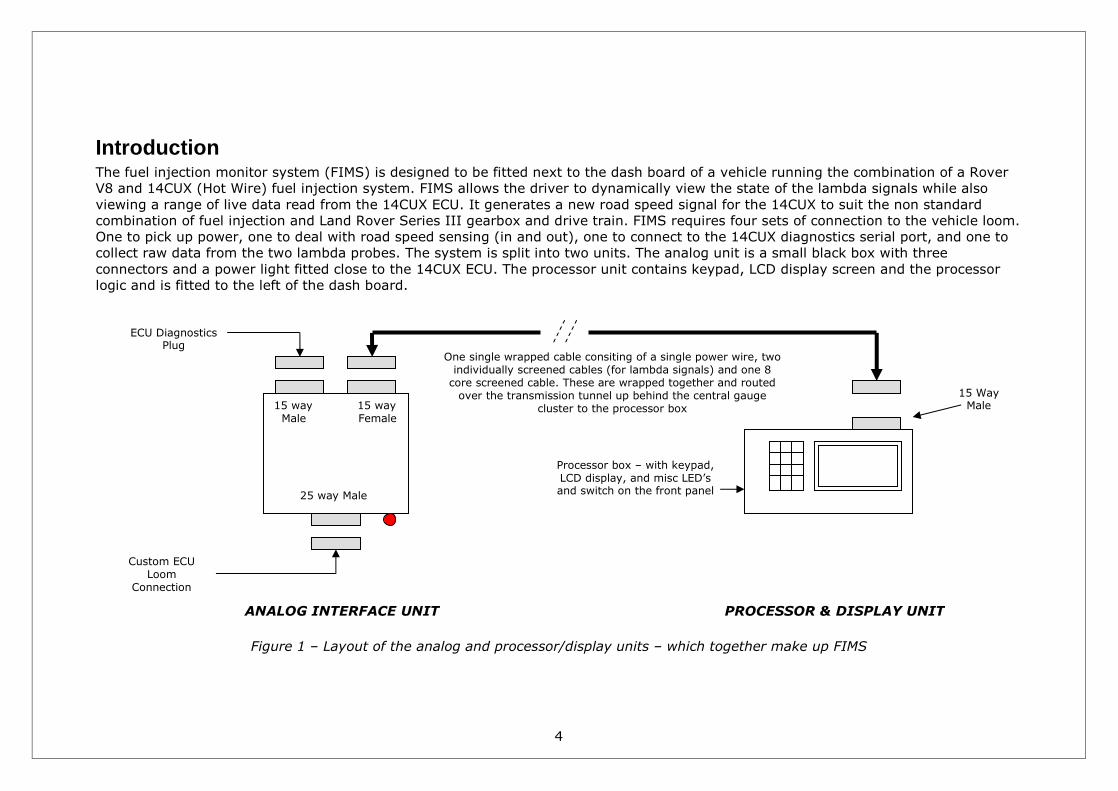
Introduction The fuel injection monitor system (FIMS) is designed to be fitted next to the dash board of a vehicle running the combination of a Rover
V8 and 14CUX (Hot Wire) fuel injection system. FIMS allows the driver to dynamically view the state of the lambda signals while also
viewing a range of live data read from the 14CUX ECU. It generates a new road speed signal for the 14CUX to suit the non standard
combination of fuel injection and Land Rover Series III gearbox and drive train. FIMS requires four sets of connection to the vehicle loom.
One to pick up power, one to deal with road speed sensing (in and out), one to connect to the 14CUX diagnostics serial port, and one to
collect raw data from the two lambda probes. The system is split into two units. The analog unit is a small black box with three
connectors and a power light fitted close to the 14CUX ECU. The processor unit contains keypad, LCD display screen and the processor
logic and is fitted to the left of the dash board.
Figure 1 � Layout of the analog and processor/display units � which together make up FIMS
15 way 15 way
Male Female
25 way Male
Custom ECU
Loom
Connection
ECU Diagnostics
Plug
Processor box � with keypad,
LCD display, and misc LED�s
and switch on the front panel
One single wrapped cable consiting of a single power wire, two
individually screened cables (for lambda signals) and one 8
core screened cable. These are wrapped together and routed
over the transmission tunnel up behind the central gauge
cluster to the processor box
15 Way
Male
ANALOG INTERFACE UNIT PROCESSOR & DISPLAY UNIT
5
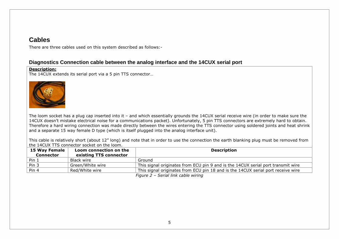
Cables There are three cables used on this system described as follows:-
Diagnostics Connection cable between the analog interface and the 14CUX serial port Description:
The 14CUX extends its serial port via a 5 pin TTS connector�
The loom socket has a plug cap inserted into it � and which essentially grounds the 14CUX serial receive wire (in order to make sure the
14CUX doesn�t mistake electrical noise for a communications packet). Unfortunately, 5 pin TTS connectors are extremely hard to obtain.
Therefore a hard wiring connection was made directly between the wires entering the TTS connector using soldered joints and heat shrink
and a separate 15 way female D type (which is itself plugged into the analog interface unit).
This cable is relatively short (about 12� long) and note that in order to use the connection the earth blanking plug must be removed from
the 14CUX TTS connector socket on the loom.
15 Way Female
Connector
Loom connection on the
existing TTS connector
Description
Pin 1 Black wire Ground
Pin 3 Green/White wire This signal originates from ECU pin 9 and is the 14CUX serial port transmit wire
Pin 4 Red/White wire This signal originates from ECU pin 18 and is the 14CUX serial port receive wire
Figure 2 � Serial link cable wiring

6
Analog interface to processor unit cable Description:
This cable connects the analog interface unit (located in the battery compartment of the vehicle), to the dash mounted processor box.
This cable is roughly 2mtrs long, and consists of four cables wrapped together. One power cable, a pair of separately screened cables (to
carry the buffered lambda signals), and a single 8 core screened cable to carry the remaining signals. The three earth screens (two from
the lambda cables, and one from the 8 core cable) are commoned to form a ground. D type connectors terminate both ends of the cable
with the end terminating near the 14CUX being male, and the end at the dash board being female.
Note that wiring adheres to the normal D type pin numbering conventions (refer to appendix A). Pin number �n� at one end will connect
to pin number �n� at the other.
15 Way Female
Connector
Description
Pin 1 and Pin 2 12V � using heavy 7amp 1mm CSA Power cable in yellow
Pin 13 and pin 14 Screen of the 8 core cable, and the screen of both lambda signal cables.
Pin 15 Lambda left signal
Pin 12 Lambda right signal
Pin 3 14CUX serial port transmit signal
Pin 4 14CUX serial port receive signal
Pin 5 EFi Check light (the signal issued by the 14CUX when a �check engine� fault occurs. Note this is active low.
Pin 6 Engine electric cooling fans on (this signal is +12v when the engine cooling fans are running).
Pin 7 Raw road speed transducer signal � as read from the transducer fitted in line with the speedometer cable
Pin 8 Road speed output signal. This is a 5v signal output from the processor unit and sent to the analog interface unit �
which then uses a darlington pair to amplify the 5v signal to swing between 12v and ground. That signal is in turn fed
out from the analog unit as an input to the 14CUX system in order to control when the vehicle switches to idle.
Pins 9, 10 and 11 Spare
Figure 3 � Cable wiring between the analog unit and the processor

7
Breakout cable for the injection loom Description:
This cable extends a set of signals from the 14CUX ECU loom, and was carefully added to the loom when the 14CUX was originally added
to the vehicle. It terminates in a 24 way female D type connector located physically close to the 14CUX main plug. Note that the FIM
system does not require all of these signals. Those that are not used by the FIM are shaded in gray.
25 Way Female
Connector
Description
Pin 1,2 and 3 Ground
Pin 4 Main relay sink drive (ECU pin 12)
Pin 5 Main relay output (ECU pin 2)
Pin 6 Fuel relay sink drive (ECU 19)
Pin 7 Fuel relay output (to fuel pump)
Pin 8 Road Speed Transducer signal output from the FIM box and fed as an input to the 14CUX. Note that this signal is
generated by the FIM processor unit.
Pin 9 Left injector sink drive signal (ECU 13)
Pin 10 Right injector sink drive signal (ECU11)
Pin 11 & 12 Spare
Pin 13 Raw road speed signal from the transducer fitted in line with the speedometer cable (note that the transducer is a two
wire unpolarised device, and the other wire connects directly to 12v)
Pin 14 Spare
Pin 15 Ignition switched +12v
Pin 16 Engine cooling fans activation signal (which is +12v when the engine cooling fans are running)
Pin 17 EFi check engine warning signal. This is the ECU signal that normally connects to a lamp on the dash board to drive a
�check engine� style warning light. Note that this is an active low signal
Pin 18,19 & 20 Spare
Pin 21 Lambda left screen wire (ie: ground)
Pin 22 Direct connection to the Lambda left signal wire (passenger side)
Pin 23 Spare
Pin 24 Direct connection to the Lambda right signal wire (drivers side)
Pin 25 Lambda right screen wire (ie: ground)
Figure 4 � ECU loom break out cable wiring

8
FIMS Analog Interface Unit The analog interface unit consists of a box with three connectors, a power LED, and a small (and very simple) circuit board. The primary
purpose of this unit is to provide three high impedence amplifiers with which to monitor firstly the left and the right lambda O2 sensor
signals, and secondly the raw road speed transducer signal. An additional darlington pair amplifier is used to amplify the 5v road speed
signal from the processor to +12v which is then fed out to the 14CUX as the road speed input.
Figure 5 � Analog interface unit - Straight through connections and power (schematic 1 of 2)
600Ω TIL209
Red LED
on box
0.1uF
63V 47uF
63V
Female DB15 Pin 1
and pin 2
Female DB15 Pin 14
and pin 13
DB25 Pin 15
ign switched +12v
DB25 Pins 1,2 + 3
Ground
Female DB15 Pin 5 DB25 Pin 17
EFi Check light
Female DB15 Pin 6 DB25 Pin 16
Eng cooling fans on
Female DB15 Pin 3
Male DB15 Pin 3
Female DB15 Pin 4
Male DB15 Pin 4
7Male DB15 Pin 1
Serial comms to 14CUX

9
Figure 6 � Analog interface unit - High impedence buffers and darlington driver (schematic 2 of 2)
2
B
C
E
560Ω
+12V
DB25 pin 15
Female DB15 Pin 8
4K7
Female DB15 Pin 7 2
6
5
7
1
3
13K
4K7
Female DB15 Pin 15
Female DB15 Pin 12
DB25 Pin 247
Left Lambda signal
DB25 Pin 22
Right lambda signal
DB25 Pin 13
Raw roadspeed
transducer signal
fed as input to this
box
DB25 Pin 8
Roadspeed signal
fed as an output
from this box to the
14CUX
13K
4K7
1
3
½ LM358 8 Pin DIL
+12v= Pin 8
Gnd=Pin 4
½ LM358 8 Pin DIL
+12v= Pin 8, Gnd=Pin 4
2x BC109
Notes:
1. Each op amp forms one half of an 8 pin dual in line IC.
2. Three opamps are used, and one is spare
3. Connect 12v (ignition switched) to op amp pin 8, and ground to pin 4
4. Use 0.1uF decoupling close to both of the IC�s
5. Wire the two lambda signals for both input AND output using individually screened cables.
6. The terms �left� and �right� can be read as when standing at the rear of the vehicle looking forward.
7. Refer to the diagram on the right for a pin view (underside) of a BC109 NPN general purpose transistor
½ LM358 8 Pin DIL
+12v= Pin 8, Gnd=Pin 4

10
FIMS Processor Unit The processor unit is designed to be dash mounted. It contains an illuminated keypad, a backlit but dimable LCD display, and a set of
four front panel LED�s. The logic is relatively simple consisting of a crystal oscillator module, a single quad two input nand gate (74LS00)
and a PIC microcontroller of type 18F4620.
The quad two input nand is used primarily as a buffer (to isolate the PIC chip from the 14CUX) but has a secondary function of acting as
a 12v inverting interface. The raw road speed signal transducer outputs a 12v signal which passes through a potential divider before
being passed into one nand and then to the PIC chip. Additionally the 14CUX serial port transmits a 12volt signal, but which is also
inverted and so that signal has to be interfaced and complimented before being passed to the PIC (note that the 14CUX receive signal
requires a non inverted +12volt signal, but in practice a 5volt signal drives it perfectly well).
The project complexity is hidden within the software programmed into the PIC chip. The key features of the PIC chip employed by this
project are�
1. Large eprom space (64K bytes)
2. Large RAM space (by microcontroller standards 3968 bytes is huge)
3. E2PROM (1K bytes) for long persistent state
4. Built in I2C bus
5. Fully programmable Asynchronous UART with interrupt support
6. Timer counters with extensive interrupt support
7. Fast analog to digital convertion with interrupt support
The PIC chip is programmed using the Microchip ICD3 system employing the short flying lead (inside the processor unit) with an RJ45
plug on the end. The software is written in C, and consumes 18KBytes of ROM and 142 bytes of RAM. E2PROM is used to hold persistent
state data.

11
Processor Unit � Front Panel LED Wiring The processor box has four LED�s mounted on the front panel (two amber, one green and one red). These are wired onto a small PCB
with current limiting resistors and a small eight wire loom as shown below. The two amber LED�s are connected to the processor and can
be used freely for debug by altering the software. The green LED illuminates when the engine cooling fans are switched on. The red LED
illuminates when the 14CUX activates its EFi �check engine� warning light.
Figure 7 � Front Panel LED wiring in the processor unit
Red (+ve) red LED
Orange (-ve) red LED
Yellow (+ve) green LED
Green (-ve) green LED
Blue (+ve) amber A LED
White (-ve) amber A LED
Black (+ve) amber B LED
Brown (-ve) amber B LED
Amber A Amber B
Notes:
Both the two amber LED�s have current limiting resistors fitted that assume +5 volt operation
Both the green and red LED�s have current limiting resistors fitted that assume +12 volt operation
12
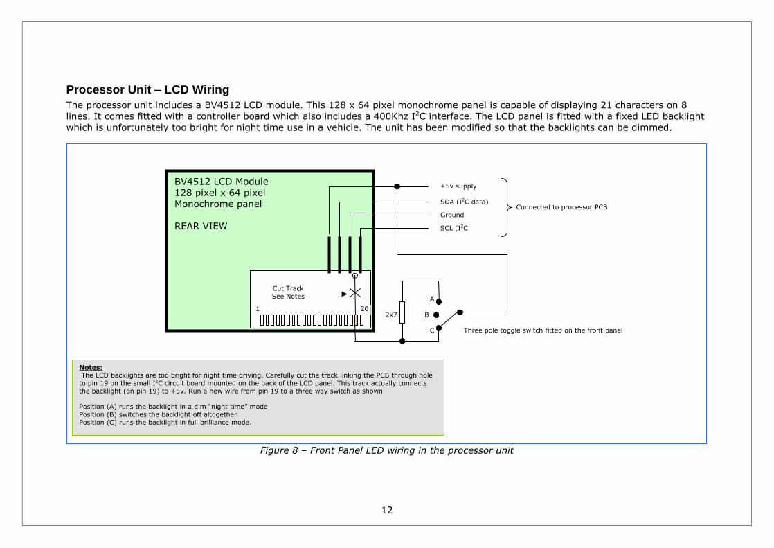
Processor Unit � LCD Wiring The processor unit includes a BV4512 LCD module. This 128 x 64 pixel monochrome panel is capable of displaying 21 characters on 8
lines. It comes fitted with a controller board which also includes a 400Khz I2C interface. The LCD panel is fitted with a fixed LED backlight
which is unfortunately too bright for night time use in a vehicle. The unit has been modified so that the backlights can be dimmed.
Figure 8 � Front Panel LED wiring in the processor unit
2k7
Connected to processor PCB
C
B
A
SDA (I2C data)
Ground
SCL (I2C
clock)
+5v supply
Notes:
The LCD backlights are too bright for night time driving. Carefully cut the track linking the PCB through hole
to pin 19 on the small I2C circuit board mounted on the back of the LCD panel. This track actually connects
the backlight (on pin 19) to +5v. Run a new wire from pin 19 to a three way switch as shown
Position (A) runs the backlight in a dim �night time� mode
Position (B) switches the backlight off altogether
Position (C) runs the backlight in full brilliance mode.
BV4512 LCD Module
128 pixel x 64 pixel
Monochrome panel
REAR VIEW
Cut Track
See Notes
Three pole toggle switch fitted on the front panel
1 20
13
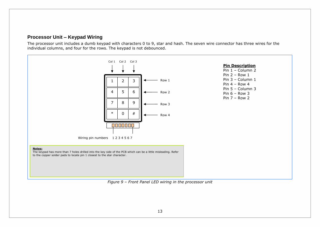
Processor Unit � Keypad Wiring The processor unit includes a dumb keypad with characters 0 to 9, star and hash. The seven wire connector has three wires for the
individual columns, and four for the rows. The keypad is not debounced.
Figure 9 � Front Panel LED wiring in the processor unit
Notes:
The keypad has more than 7 holes drilled into the key side of the PCB which can be a little misleading. Refer
to the copper solder pads to locate pin 1 closest to the star character.
1 2 3
4 5 6
7 8 9
* 0 #
Wiring pin numbers 1 2 3 4 5 6 7
Row 1
Row 2
Row 3
Row 4
Col 1 Col 2 Col 3
Pin Description
Pin 1 � Column 2
Pin 2 � Row 1
Pin 3 � Column 1
Pin 4 � Row 4
Pin 5 � Column 3
Pin 6 � Row 3
Pin 7 � Row 2
14
Processor Unit � Schematic. The processor unit schematic is shown on the following page. The circuit board contains a set of pins which act as soldered connectors.
The wiring to the LCD panel, the keypad, the LED�s and the 15 way D type are soldered to these connectors. The connections are shown
below.
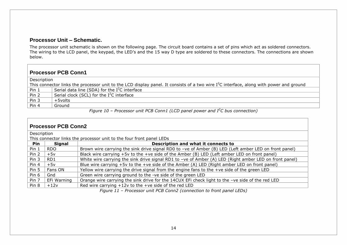
Processor PCB Conn1 Description
This connector links the processor unit to the LCD display panel. It consists of a two wire I2C interface, along with power and ground
Pin 1 Serial data line (SDA) for the I2C interface
Pin 2 Serial clock (SCL) for the I2C interface
Pin 3 +5volts
Pin 4 Ground
Figure 10 � Processor unit PCB Conn1 (LCD panel power and I2C bus connection)
Processor PCB Conn2 Description
This connector links the processor unit to the four front panel LEDs
Pin Signal Description and what it connects to
Pin 1 RDO Brown wire carrying the sink drive signal RD0 to �ve of Amber (B) LED (Left amber LED on front panel)
Pin 2 +5v Black wire carrying +5v to the +ve side of the Amber (B) LED (Left amber LED on front panel)
Pin 3 RD1 White wire carrying the sink drive signal RD1 to �ve of Amber (A) LED (Right amber LED on front panel)
Pin 4 +5v Blue wire carrying +5v to the +ve side of the Amber (A) LED (Right amber LED on front panel)
Pin 5 Fans ON Yellow wire carrying the drive signal from the engine fans to the +ve side of the green LED
Pin 6 Gnd Green wire carrying ground to the -ve side of the green LED
Pin 7 EFi Warning Orange wire carrying the sink drive for the 14CUX EFi check light to the �ve side of the red LED
Pin 8 +12v Red wire carrying +12v to the +ve side of the red LED
Figure 11 � Processor unit PCB Conn2 (connection to front panel LEDs)
15
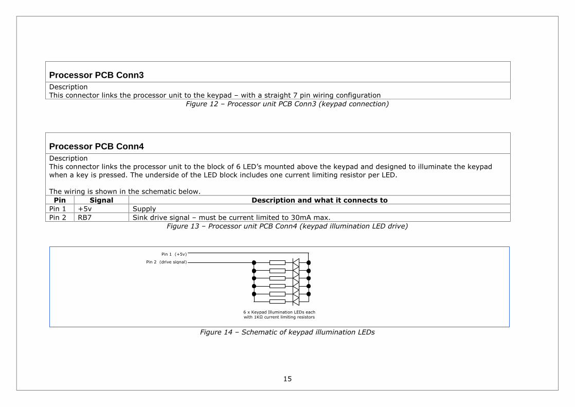
Processor PCB Conn3 Description
This connector links the processor unit to the keypad � with a straight 7 pin wiring configuration
Figure 12 � Processor unit PCB Conn3 (keypad connection)
Processor PCB Conn4 Description
This connector links the processor unit to the block of 6 LED�s mounted above the keypad and designed to illuminate the keypad
when a key is pressed. The underside of the LED block includes one current limiting resistor per LED.
The wiring is shown in the schematic below.
Pin Signal Description and what it connects to
Pin 1 +5v Supply
Pin 2 RB7 Sink drive signal � must be current limited to 30mA max.
Figure 13 � Processor unit PCB Conn4 (keypad illumination LED drive)
Figure 14 � Schematic of keypad illumination LEDs
Pin 1 (+5v)
Pin 2 (drive signal)
6 x Keypad Illumination LEDs each
with 1KΩ current limiting resistors
16
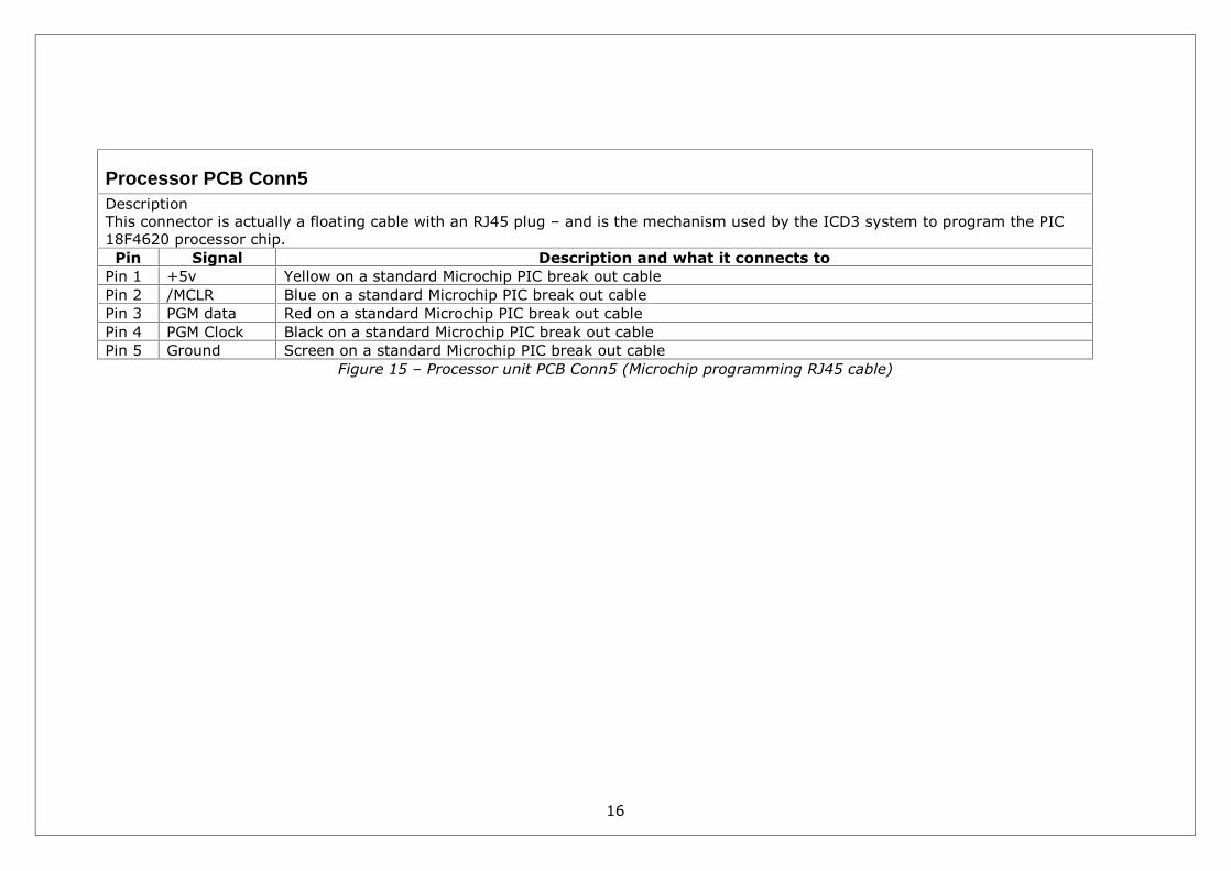
Processor PCB Conn5 Description
This connector is actually a floating cable with an RJ45 plug � and is the mechanism used by the ICD3 system to program the PIC
18F4620 processor chip.
Pin Signal Description and what it connects to
Pin 1 +5v Yellow on a standard Microchip PIC break out cable
Pin 2 /MCLR Blue on a standard Microchip PIC break out cable
Pin 3 PGM data Red on a standard Microchip PIC break out cable
Pin 4 PGM Clock Black on a standard Microchip PIC break out cable
Pin 5 Ground Screen on a standard Microchip PIC break out cable
Figure 15 � Processor unit PCB Conn5 (Microchip programming RJ45 cable)

17
Processor unit DB15 Chassis Mounted Male Plug Description
This male chassis mounted connector is on the back of the processor unit, and (via the long linking cable) connects the processor to
the analog unit.
Pin Description
Pin 1 and Pin 2 ignition switched +12v
Pin 13 and pin 14 Ground
Pin 15 Buffered Lambda left signal
Pin 12 Buffered Lambda right signal
Pin 3 14CUX serial port transmit signal
Pin 4 14CUX serial port receive signal
Pin 5 EFi Check light (the signal issued by the 14CUX when a �check engine� fault occurs. Note this is active low.
Pin 6 Engine electric cooling fans operating (this signal is active high and is asserted when the cooling thermostat
senses an over temperature condition).
Pin 7 Buffered raw road speed transducer signal � as read from the transducer fitted in line with the speedometer
cable
Pin 8 Road speed output signal. This is the 5v signal output from the processor unit to the analog interface unit �
which uses a darlington pair to amplify the signal to swing between 12v and ground. That signal is in turn fed
as an input to the 14CUX system in order to control when the 14CUX switches the vehicle to idle.
Pins 9, 10 and 11 Spare
Figure 16 � Processor unit rear chassis mounted 15 way male D type

18
Figure 17 � FIMS Prototype PCB layout
OSC
74LS00
PIC 18F4620
Conn1 LCD
1. SDA
2. SCL
3. +5v
4. Ground
1
2
3
4
14CUX Serial bus
1. Ground
2. 14CUX Serial interface transmit
(from ECU pin 9)
3. 14CUX Serial interface receive
(from ECU pin 18)
1
2
3
1
2
1
2
Conn4 (keypad illumination)
1. +5v
2. LED sink drive signal
Road speed signals
1. Raw road speed in
2. Road speed signal output (to 14CUX)
Conn3 (keypad)
1. Keypad 1
2. Keypad 2
3. Keypad 3
4. Keypad 4
5. Keypad 5
6. Keypad 6
7. Keypad 7
Conn2 (Front LEDS)
1. RD0 output
2. +5v
3. RD1 Output
4. +5v
5. Engine fans
6. Ground
7. EFi warning light
8. +12v
1
2
3
4
1
2
3
4
5
6
7
5
6
7
8
Lambda probe inputs
Both of these pins are grounded (for the lambda screens)
Lambda probe inputs
Left lambda input (DB15 pin 15)
Lambda probe inputs
Right lambda input (DB15 pin 12)
Yellow & Black wires
To 15 way connector +12v and
ground.
Yellow, Black & Red wires
To 3 pin 7805 voltage regulator
(red is +5v out)

19
Figure 18 � FIMS Processor logic schematic
8
12 31
Vss Vss
1
In Out
PIC 18F4620
RC1
4. PGM-PGC
3. PGM-PGD
2. /MCLR
1. +5
RJ45 CONN 5
3 x 11K
½ 74LS00
10
9
13
12
25 RC6
RC7 26
2
3
RA0
RA1
17 RC2
16
¼ 74LS00
5
6
4 DB15 Pin 7
raw road
speed signal
input
5K6
RB0
RD1
19
20
7
14
8
13
CONN 2
CONN 4
(Keypad LEDs)
CONN 3 Keypad
DB15 pins 1+2
+5v
33
34
35
36
37
38
40
39
RB1
RB2
RB3
RB4
RB5
RB6
RB7
RD0
2K2
Vdd
RC3
RC4
23
18
1
3. +5v
1. SDA
2. SCL
4. GND
2x5K6 10K
0.1uF
63V
32 11
0.1uF
63V
0.1uF
63V
GND DB15
Pins 14+13
10uF
16V
+5 Vdd 7805
47uF
63V
CONN 1 (LCD)
/MCLR
Vdd
Keypad pin 1
Keypad pin 2
Keypad pin 3
Keypad pin 4
Keypad pin 5
Keypad pin 6
Keypad pin 7
DB15 pin 6
DB15 pin 5
8Mhz
Osc Module
14 Pin DIL
933Ω
DB15 Pin 8
road speed
signal output
DB15 Pin 15
Left Lambda
DB15 Pin 12
Right Lambda Note the use of individually screened cables for both lambda signals
¼ 74LS00
2
3
1
430Ω
DB15 Pin 3
14CUX Serial
port Transmit
signal
8 11 DB15 Pin 4
14CUX Serial
port receive
signal
Notes:
1. 74LS00 is a 14 pin dual in line package. Connect Vdd pin 14, Vss pin 7
2. DIL packages are each decoupled with 0.1uF disc capacitors
3. 7805 regulator is bolted phycially and electrically to the chassis
4. Processor is a PIC 18F4620 in a 40 pin dual in line package
5. GND
Common
2
3
4
5
6
7
1
2
+12v DB15
Pins 1+2

20
Appendix A � D Connector Pin Numbering
Figure 19 � D-Type Connector Wiring Pin Numbering
25 ------------------------------------- 14 14 ------------------------------------- 25
13 ---------------------------------------- 1 1 ---------------------------------------- 13
15 ------------------ 9
8 7 6 5 4 3 2 1 1 2 3 4 5 6 7 8
9 8 7 6 6 7 8 9
5 4 3 2 1 1 2 3 4 5
FEMALE D CONNECTOR - SOLDER BUCKET VIEW MALE D CONNECTOR - SOLDER BUCKET VIEW
9 ------------------ 15

21
Appendix B � TTS Plug Wiring When a diagnostic unit is plugged into the 14CUX TTS loom plug, the following wiring layout is used.
Figure 20 � TTS wiring for a diagnostic unit
14CUX receive signal
(input to 14CUX with +5v swing)
14CUX transmit signal
(output from 14CUX with +12v swing)
Ground
Notes:
This is the pin view looking at the diagnostics plug on the diagnostic reader (with the cable exiting at the
rear). The mirror connections would apply to the socket on the ECU wiring loom.