Fuel Cell Stack CVM Chip Solder Joint Structural … Cell Stack CVM Chip Solder Joint Structural...
14
Fuel Cell Stack CVM Chip Solder Joint Structural Analysis with ANSYS Sub-Modeling Technique Kemal Ozgur, Ph.D., P.Eng. Senior Engineer Ballard Power Sysems John Kenna Manager, Product Development Ballard Power Systems Abstract Structural analysis tools have been used to investigate stress conditions for electronic components used in fuel cells subjected to tough environmental conditions such as heat and moisture. The Cell Voltage Monitoring (CVM) system is an example of electronic device used in fuel cell stacks that provide the essential service of monitoring the voltages produced by cells during operation. Failure of the CVM electronics could signal false cell performance and send inconsistent signals to the vehicle control unit. The electrical circuit boards need to be compatible with fuel cell temperature and moisture condition that are dependant on operation drive cycles from the vehicle. These cycles directly impact the active electrical components that are attached to printed circuit board, and through the use of finite element analysis tools can be investigated to insure mechanical compliance. Introduction The Ballard MK9 series stacks are for automotive applications, therefore the stacks and its components, including the CVM (Cell Voltage Monitoring) are subject to environmental conditions such as high humidity and temperature. Finite element model of the CVM assembly was built to calculate the stress on the CVM electronic components’ solder joints. CVM board deflections due to thermal expansion of the board itself and the surrounding potting material were calculated. High stress areas and components were identified on this assembly model. Then, Sub-modeling technique provided by ANSYS was utilized to model individual chips of interest with all details. This technique is a powerful tool for quickly identifying the failure modes that could result in CVM chip failures. The difference in CTE of the potting material that protects the CVM from the environment and the PCB was identified as probable areas, where excessive stress could cause early failures of CVM components. Once the high stress area was determined, new potting material with suitable CTE (that’s close to the PCB and chips’ CTE) was selected, eliminating the stress components for the CVM chip, and averting failures. Other solutions such as mechanical staking and mounting arrangements were investigated to allow the design department options for packaging the CVM board. Analysis The analysis concentrated on two elements of the CVM design, i) Understand the structural loading on electronic components during thermal cycling ii) Characterize the two different types of potting material
Transcript of Fuel Cell Stack CVM Chip Solder Joint Structural … Cell Stack CVM Chip Solder Joint Structural...

Fuel Cell Stack CVM Chip Solder Joint Structural Analysis with ANSYS Sub-Modeling Technique
Kemal Ozgur, Ph.D., P.Eng. Senior Engineer
Ballard Power Sysems John Kenna
Manager, Product Development Ballard Power Systems
Abstract
Structural analysis tools have been used to investigate stress conditions for electronic components used in fuel cells subjected to tough environmental conditions such as heat and moisture. The Cell Voltage Monitoring (CVM) system is an example of electronic device used in fuel cell stacks that provide the essential service of monitoring the voltages produced by cells during operation. Failure of the CVM electronics could signal false cell performance and send inconsistent signals to the vehicle control unit. The electrical circuit boards need to be compatible with fuel cell temperature and moisture condition that are dependant on operation drive cycles from the vehicle. These cycles directly impact the active electrical components that are attached to printed circuit board, and through the use of finite element analysis tools can be investigated to insure mechanical compliance.
Introduction The Ballard MK9 series stacks are for automotive applications, therefore the stacks and its components, including the CVM (Cell Voltage Monitoring) are subject to environmental conditions such as high humidity and temperature. Finite element model of the CVM assembly was built to calculate the stress on the CVM electronic components’ solder joints. CVM board deflections due to thermal expansion of the board itself and the surrounding potting material were calculated. High stress areas and components were identified on this assembly model. Then, Sub-modeling technique provided by ANSYS was utilized to model individual chips of interest with all details. This technique is a powerful tool for quickly identifying the failure modes that could result in CVM chip failures. The difference in CTE of the potting material that protects the CVM from the environment and the PCB was identified as probable areas, where excessive stress could cause early failures of CVM components. Once the high stress area was determined, new potting material with suitable CTE (that’s close to the PCB and chips’ CTE) was selected, eliminating the stress components for the CVM chip, and averting failures. Other solutions such as mechanical staking and mounting arrangements were investigated to allow the design department options for packaging the CVM board.
Analysis
The analysis concentrated on two elements of the CVM design,
i) Understand the structural loading on electronic components during thermal cycling
ii) Characterize the two different types of potting material

Figure 1 illustrates a typical CVM assembly on a MK902 fuel cell stack. The analysis concentrates on the CVM box and the PCB board inside it (Fig.2). As the fuel cell stack operates in a humid environment the PCB needs protection from moisture by utilizing potting materials such as silicone and epoxy resins. Table 1 lists the material properties of the CVM components that were part of the FEA analysis.
Figure 1. CVM Assembly on a Fuel Cell Stack with CVM Cell Pickup Detail
Figure 2. CVM Internals; the PCB
CVM Box

Table 1. Material Properties
Modulus of Elasticity
Poisson’s Ratio Density [kg/m^3] Strength
[MPa]
CTE [1/C]
PCB Board 15.3 GPa 0.4 5017 - 1.8e-5
Silicone Potting Compound
0.706 MPa 0.45 979.26 0.31 27.3e-5
Epoxy Resin Potting Compound
12 GPa 0.4 1800 125 2.0e-5
Enclosure (PBT) 7 GPa 0.37 1350 80 5.2e-5
Chip 20 GPa 0.45 2000 - 1.8e-5
Lead (steel) 205 GPa 0.27 7872 413 1.26e-5
Solder
(63Sn-37Pb)
32GPa 0.38 8400 Yield 43
Ultimate 52
2.47e-5
The CVM analysis was done by modeling the chips with all the details including individual solder pad, lead details. The entire CVM assembly is modeled with relatively coarse mesh (Fig.5). Sub-modeling technique is used for individual chip/solder joint detail analysis. Each solder/lead joint is modeled separately. The solder geometry is created based on actual solder cross section pictures (Fig.3). The sub-model uses the calculated displacement results of CVM assembly model as boundary conditions at the “cut interface” (Fig.4).
Figure 3. CVM Chip Solder Joint Cross Sections

Figure 4. CVM Chip Sub-Model
Silicon
PCB
Chip
Lead
Solder
PCB
Cut Interface
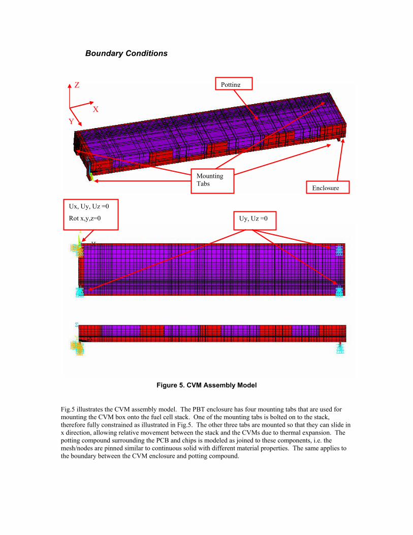
Boundary Conditions
Figure 5. CVM Assembly Model
Fig.5 illustrates the CVM assembly model. The PBT enclosure has four mounting tabs that are used for mounting the CVM box onto the fuel cell stack. One of the mounting tabs is bolted on to the stack, therefore fully constrained as illustrated in Fig.5. The other three tabs are mounted so that they can slide in x direction, allowing relative movement between the stack and the CVMs due to thermal expansion. The potting compound surrounding the PCB and chips is modeled as joined to these components, i.e. the mesh/nodes are pinned similar to continuous solid with different material properties. The same applies to the boundary between the CVM enclosure and potting compound.
Mounting Tabs
Y X
Z
Ux, Uy, Uz =0
Rot x,y,z=0 Uy, Uz =0
Enclosure
Potting

Elements and Meshing Technique
Solid 185 was used to mesh the entire assembly model. The entire assembly model was divided to sub-volumes that are suitable for mapped brick meshing. Fig.5 illustrates these sub volumes not the mesh. This technique helps keep the mesh size reasonable, which allows a lot faster solutions and more iterations run in a shorter time. By modeling it this way the model size was kept just below 100K DOF.
The sub-model that captures all the chip/solder details was modeled with tets Solid 187.
Analysis techniques and results of several variations of the CVM designs are discussed next. They are covered under two main subsections, Silicon Potting and Epoxy Resin Potting.
Silicon Potting Analysis
Three load cases were run for the silicon potting:
1) Rev3.0 CVM potted with silicon & PCB board bolted down to CVM enclosure
2) Rev3.0 Non-Potted CVM with PCB board bolted down to CVM enclosure
3) Rev3.0 CVM potted with silicon & PCB board not bolted to CVM enclosure (floating PCB)
The results of these load cases are illustrated in Fig.7 and the following is a high level summary.
Load Case 1) results that are based on sub-model analysis of Chip # U706 indicated high stress on its Pin#7 that exceeds solder material ultimate strength of 52MPa. This was due to thermal expansion of silicone potting compound causing the circuit board to deflect.
Load Case 2) and 3) were run to find solution to the high stress problem of Pin#7 of U706 (Fig.8&9). The other chips, U106-U606, also indicated high stress on the CVM assembly model but U706 was the worst therefore the sub-model analysis concentrated on U706.
LC 2) with non-potted CVM also indicated stress on the back side of the solder pad that exceeds solder material yield strength. This is primarily due to the difference in CTE of PCB board and enclosure.
LC 3) with PCB floating inside silicone potting indicated high stress as well. The potting compound expands non-symmetrically in this case by bulging out through the side openings (for the flex traces) of the enclosure (Fig.6). The solution for this problem is to stiffen up the enclosure sidewall and reduce the size of the openings to eliminate/reduce the “bulging” effect.
The stress concentration towards the back of the solder pad (Fig.9) is consistent with the failure shown on solder X-section pictures illustrated on Fig.3. This way, the analysis results were correlated to real life testing as pictures illustrated in Fig.3 are X-sections of run CVMs that solder joint failures.
As silicon potting creates undesirably high stress on the CVM chips, alternative potting compound that doesn’t expand as much as the silicone compound has been identified. This is an epoxy based potting compound that has very low CTE 2e-5/C, that is also very close to the PCB’s CTE 1.8e-5/C. The analysis of the epoxy resin potting compound is discussed in the following sections.

Figure 6. Potted CVM with “Floating” Circuit Board Deflections [m]
U706 U606U106 U206 U306 U406 U506U12 U13

Figure 7. CVM Assembly Model U106-U706 Max Stress vs. Load Case
Figure 8. “Floating” Circuit Board Deflections [m]
0
20
40
60
80
100
120
140
U106 U206 U306 U406 U506 U606 U706
Stre
ss [M
Pa]
Expansion of Everything(Screw Slip Joint)
No Screws
Expansion of Potting Only
No Potting

a) Yield Stress 43MPa b) Ultimate Stress 52MPa
Figure 9. U706 Pin#7 Solder Stress
Epoxy Based Potting Analysis Unlike silicone potting compound the CTE of epoxy resin potting compound is 2e-5/C that is very close to the PCB’s CTE which is 1.8e-5/C. Therefore Epoxy based potting compound doesn’t “bulge” out of the enclosure openings like silicone potting. In this case the enclosure CTE (5.2e-5/C) is higher than the potting compound, therefore the enclosure expands more than the potting especially in longitudinal direction which creates a new problem that is unique for the epoxy potting compound. The potting and the enclosure act like “bimetal”, therefore the mid-point of the CVM sags about 0.38 mm at 80C. Bending of the PCB creates additional stress on the chips. Figs.10 and 11 illustrate CVM deflection and stress respectively at 80C temperature. Fig.12 illustrates sub-model results for chip U206 that based on coarse mesh analysis (Fig.11) has the highest stress due to bending of the PCB board. When compared with Silicon potting the stress on the chips with Epoxy based potting compound is more uniformly distributed. There were a few load cases run for this design as well. The results are illustrated in a summary chart in Fig. 17. Since the difference in CTE of Epoxy potting compound and CVM enclosure results with extra stress on the chips due to bending of the CVM board, a case where the enclosure is eliminated is of interest. The calculations are run without the enclosure and in this case the CVM expands linearly without any bending (Fig.15). In this case the amount of bending, which this time is because of the difference in CTEs of the PCB and Epoxy, is minimal about 15 µm in vertical direction. Therefore stress distribution on the leads is very uniform. Sub-model results show lower stress on solder joint when bending of PCB is eliminated (Fig.16). The red color indicates areas where the material is stressed to its ultimate strength. This is limited to areas with sharp corners only, which in reality does not exist. The calculated max stress in this case is 55MPa, comparing to non-potted CVM stress of 84MPa and silicone potted CVM stress of 180MPa this is a dramatic improvement.
Testing of CVMs potted with epoxy based resin showed no sign of solder joint failure at all. This proves there is a good correlation between modeling and Design Verification (DV) testing.

Figure 10. Deflection [m] of CVM at 80C (max 0.382mm)
Figure 11. Component Stress [Pa] at 80C
Scaled to 52MPa Max Stress=74Mpa

Figure12. U206 Sub-model Stress [Pa]
Scaled to 43MPa Solder Material Yield Strength
a) Solder Pad Yield Stress (Scaling:43MPa) b) X-Section Showing Surface Yielding
Figure13. U206 Pin1 Solder Pad Yield Stress
The worst pin (Pin1)

Figure14. U206 Pin1 and 2 Solder Pad Ultimate Stress (52MPa)
Figure 15. Thermal Expansion of CVM Figure16. Epoxy Potting With No Potted with Epoxy Potting with no Enclosure Enclosure U206 Pin1 Stress (Max Deflection 0.363mm) Distribution, Scaled to 52MPa
Curved back part of the solder pad breaking due to thermal stress at 80C

0
20
40
60
80
100
120
140
160
180
200
No Potting Silicone Potting Pelnox Potting Pelnox with No-Enclosure
Stre
ss [M
Pa]
The Best
The Worst
Curved Top/BackEnd of Solder Breaking
Figure17. Summary of Results
Max Stress vs. Load Case
Conclusion Encapsulation and potting techniques were tried on CVMs as a measure of isolating the electronic components on the PCB from the humid environment they operate in. Considering Epoxy Resin and Silicon as potting compounds, Epoxy performs a lot better than Silicone since it’s thermally more compatible with the rest of the CVM components. The thermal loading is lower with Epoxy since its CTE is very close to PCB’s CTE. Eliminating the enclosure from the CVM design or using material that has similar thermal properties to Epoxy was also investigated since this further reduces the stress on the chips by eliminating the PCB bending at elevated temperature. The following is a high level summary of the analysis and also contains recommendations that were passed onto the design team as design solutions:
i) Epoxy resin potting compound is more compatible with the current CVM design as it doesn’t exert additional thermal expansion stress on the CVM components. Peak stress is reduced more than three times with Epoxy potting which eliminates the root cause of solder joint failures. ii) The enclosure forces the CVM in bending at elevated temperatures. Increasing enclosure stiffness may help for the potting process (such as straightness of final potted CVM assy.) but will putt additional stress on the CVM electronic components in operation (enclosure/potting bi-metal behavior). iii) Eliminating the enclosure, and potting or molding the CVM mounting features at the same time with the rest of the potting is recommended.
Epoxy Potting Epoxy Potting / No Enclosure
iv) If eliminating the entire enclosure is not possible post machining enclosure back/bottom gives the same functionality. v) Choosing enclosure material that has a CTE that’s closer to the potting material will also eliminate/decrease the stress related to “bi-metal” phenomenon. vi) Epoxy based potting compound is very stiff, therefore the CVM will not have structural integrity problem when subjected to vehicle road induced dynamic loads as CVM assembly’s first mode is at 233Hz.
References 1. ASM Handbook Volume 2. Properties and Selection: Nonferrous Alloys and Special-Purpose
Materials, J.R.Davis, 1990
2. Advanced Strength and Applied Elasticity, A.C. Ugural, S.K. Fenster, Second Edition Elsevier Science Publishing Co., Inc., 1987
3. Applied Strength of Materials, R.L. Mott, Second Edition, Prentice-Hall, Inc. 1990.
4. ANSYS Structural Analysis Guide, Module 6, Submodeling, ANSYS, Inc., October 30, 2001