FT8U100AX Seven Port USB Hub Controller with Embedded ... · The operation of this block is...
25
FT8U100AX High Integration 7- Port USB Hub Controller with embedded peripheral functions Future Technology Devices Intl. FT8U100AX Product Data Rev 0.90 Page 1 FT8U100AX Seven Port USB Hub Controller with Embedded Peripheral Functions Data Sheet Future Technology Devices International Limited St. George’s Studios 93/97 St. George’s Road Glasgow G3 6JA UK Friday, 31 March 2000 OBSOLETE
Transcript of FT8U100AX Seven Port USB Hub Controller with Embedded ... · The operation of this block is...
FT8U100AXHigh Integration 7- Port USB Hub Controller with embedded peripheral functions
Future Technology Devices Intl. FT8U100AX Product Data Rev 0.90 Page 1
FT8U100AX Seven Port USB Hub Controllerwith Embedded Peripheral Functions
Data Sheet
Future Technology Devices International Limited
St. George’s Studios93/97 St. George’s Road
Glasgow G3 6JAUK
Friday, 31 March 2000
OBSOLETE
FT8U100AXHigh Integration 7- Port USB Hub Controller with embedded peripheral functions
Future Technology Devices Intl. FT8U100AX Product Data Rev 0.90 Page 2
Table of Contents
1. INTRODUCTION..................................................................................................................................................3
1.1 FEATURES...........................................................................................................................................................31.2 GENERAL DESCRIPTION .......................................................................................................................................31.3 FT8U100AX BLOCK DIAGRAM ...........................................................................................................................4
2. FT8U100AX – PACKAGE & PINOUT.................................................................................................................6
2.1 FT8U100AX - PINOUT CONFIGURATION DIAGRAM .............................................................................................62.2 FT8U100AX - PINOUT DESCRIPTION...................................................................................................................72.3 FT8U100AX – PACKAGE MECHANICAL DRAWING...............................................................................................8
3. ELECTRICAL SPECIFICATIONS......................................................................................................................9
3.1 ABSOLUTE MAXIMUM RATINGS ...........................................................................................................................93.2 DC CHARACTERISTICS ( AMBIENT TEMPERATURE = 0 .. 70 DEGREES C )..............................................................93.3 AC SWITCHING CHARACTERISTICS ....................................................................................................................103.4 USB TRANSCEIVER A/C CHARACTERISTICS .......................................................................................................12
4. INTERNAL IO REGISTER SUMMARY...........................................................................................................14
4.1 USB DOWNSTREAM REGISTERS .........................................................................................................................144.2 USB SUSPEND REGISTERS .................................................................................................................................164.3 USB UPSTREAM REGISTERS...............................................................................................................................164.4 USB DEVICE/ENDPOINT REGISTERS...................................................................................................................174.5 CHIP CONTROL REGISTERS ................................................................................................................................19
APPENDIX A - FT8U100AX INTERNAL PERIPHERALS..................................................................................22
1. DRIVER SUMMARY ..............................................................................................................................................222. DEVICE END POINT ORGANISATION .....................................................................................................................233. USB AND LEGACY DEVICE LED ENCODING.........................................................................................................24
DISCLAIMER & CONTACT INFORMATION....................................................................................................25
APPLICATION SCHEMATICS – current application schematics for the FT8U100AX can be found on FTDI’shome page at http://www.ftdi.co.uk. follow the links from the Products or Support pages.
OBSOLETE

FT8U100AXHigh Integration 7- Port USB Hub Controller with embedded peripheral functions
Future Technology Devices Intl. FT8U100AX Product Data Rev 0.90 Page 3
1. Introduction
1.1 Features
• High integration USB hub controller
• 7 x Downstream and 1 x Upstream USB Hub
Ports
• Embedded Peripherals Including …
- RS232 Serial Port
- PS/2 Keyboard Port
- PS/2 Mouse Port supporting –
2 Button PS/2 Mouse
3 Button PS/2 Mouse
Thumb-Wheel PS/ 2 Mouse
- IrDA SIR Port
- Ir Remote Control Port
- Master/Slave 2-Wire Serial Bus
• 2 Status LEDs per USB Port indicates
- High / Low Speed Peripheral
- USB Peripheral Bus Traffic
- Peripheral Over-Current Error
- Peripheral Babble / EOF Error
- USB Reset Condition
- USB Suspend Condition
• Power Control / Overload detect on each
individual USB port
• External Firmware in OTP ROM
• 3.3v Supply Operation
• UHCI / OHCI Compliant
• USB 1.1 Specification Compliant
• 100 Pin PQFP package
1.2 General Description
The FT8U100AX is a 7-Port stand-alone USB hub controller IC with firmware in external OTP ROM for
maximum flexibility and product differentiation. It’s high integration includes an advanced USB 7-Port Hub
controller, EMCU micro-controller core and a variety of embedded peripheral ports allowing a wide variety of
legacy and other peripherals to be connected to and controlled by a USB enabled system through a
FT8U100AX based hub.
The FT8U100AX has power control and over-current detect on each of the 7 downstream ports and
features 2 status LEDs per port providing a useful diagnostic aid for peripherals plugged into the hub ports.
A wide range of pre-tested firmware is available from FTDI including 4 and 7 Port hub solutions with
support for legacy keyboards and mice and RS232 serial peripherals. Legacy keyboards and mice plugged into
the PS/2 ports are translated by the into USB HID 1.0 compliant protocol whilst firmware and Windows ’98
drivers are available for the RS232 serial port function.
A range of tested standard reference designs is available to compliment the firmware and ensure ease
of design and fast time to market.
The FT8U100AXintegrates all the above functions into a single cost effective 100 pin PQFP package,
requiring only external power switches and a few components to complete the design.
OBSOLETE
Future Technology Devices Intl. FT8U100AX Product Data Rev 0.90 Page 4
1.3 FT8U100AX Block Diagram
EMCUMICROCONTROLLER
CORE
DATA SRAM256 Bytes
RA0 - RA14
ROE#,RCE#
Internal DataBus
RD0 - RD7
ExternalROM Bus
ADDR
CTL
DATA
FTDISERIAL INTERFACE
ENGINE( SIE )
ENDPOINT DATABUFFER256 Bytes
USBUPSTREAM
PORT
UP1+,UP1-
USB HUB REPEATEREOF LOCK ANDBABBLE ERROR
DETECT
USBDOWNSTREAM
PORTS
DN1+,DN1- toDN7+, DN7-
HUB PORTPOWER CONTROL
AND OVERCURRENT
DETECT
PWR1# - PWR7#
OVL1# - OVL7#
SERIAL PORT 1SERIAL PORT 2
( IrDA SIR )SERIAL PORT 3
( CIR )SPRX,IRRX,CRTXL/H
SPTX,IRTX,CRTX
PARALLELI/O PORTS
1 - 5
P1D0 to P1D7,P2D0 to P2D6,P3D0 to P3D6,P4D0 to P4D6,P5D0 to P5D5
NOTE : SOME OF THE PARALLEL PORTIO PINS ARE MULTIPLEXED WITH
OTHER SIGNALS( SEE PINOUT DIAGRAM FOR DETAILS )
MASTER / SLAVE2-WIRE
SERIAL BUS
PS/2 KEYBOARD I/F
PS/2 MOUSE I/F
SCL, SDA
MDAT,KDAT
MCLK,KCLK
INT
FTIRIr REMOTE CONTROL
PORT
FTIR
OSC48MHz XTIN
XTOUT
FT*U!))AX INTERNAL BLOCK DIAGRAM
OBSOLETE
Future Technology Devices Intl. FT8U100AX Product Data Rev 0.90 Page 5
1.4 Block Summary
EMCU Microcontroller Core - FTDI’s 8 bit Embedded Microcontroller provides an easy to program , efficient Harvardarchitecture CPU with 256 bytes of data memory (SRAM). The op-codes are optimised for USB applications and theEMCU includes several standard on board peripherals including serial I/O with modem control and baud rate generator,ISA bus peripheral interface and PS/2 keyboard and mouse interface.
The data sheet for the FTDI EMCU microcontroller core is available on request.
OSC 48MHz – The FTF8U100AX supports the use of either a 48 MHz oscillator or a crystal. , as preferred based oncost versus additional tuning circuit logic. Appendix B contains reference schematics using a 48MHz crystal – includinga bandpass filter network and DC blocking capacitor (L1 and C4 with C5 on UH8340 application schematic inAppendix B) advised for reliable operation at 48MHz. Alternatively a 48MHz oscillator can be connected to XTIN usinga 10 Ohm series resistor and with the option to add a smoothing capacitor to ground.
Data SRAM - 256 bytes of local variable memory.
FTDI Serial Interface Engine - the FT8U100AX contains an SIE block which provides the following USB functions -integral DPLL Data Separator, NRZI Encode/Decode, Bit Stuff/Unstuff, Sync Packet Generation and Detection, EOPand Bus Reset Detect, Parallel <-> Serial Conversion, CRC checking and generation, PID decode and Validation,Packet Level Handshaking, Suspend/Resume Detection and Signalling
USB Hub Repeater - this block provides the data routing functionality for the FT8U100AX. This provides, on a per-portbasis, Connect and Disconnect functions, Full / Low Speed Signal Routing, Power Control and Overcurrent Detect,Suspend and Resume Control as well as Babble detection, End Of Frame Timer and Lock Generation, Low Speed“Keep Alive Strobe” Generation and Low Speed Data Conversion and Pre-Packet Decode.
Hub Port Power Control - this block provides Power Control and Overcurrent Detect functions. The FTDI USB Hubfirmware implements several features aimed at improving USB Hub product performance and error reporting insituations where third party peripherals cause power glitches and USB current violations.
Endpoint Data Buffer - 256 byte data buffer with expandable endpoint count, providing support for USB devices withinthe IC. This provides endpoint buffer management, transmit and receive counters and address to endpoint decoding.The operation of this block is discussed further in section 4.4, USB Device/EndPoint Registers and Appendix A, part 2– where EndPoint Data Buffer organisation for the UltraHub reference design is discussed.
Parallel I/O Ports - this FT8U100AX provides several General Purpose I/O Ports. These bidirectional ports can beused to tailor the functionality of Hub products using the F8U100AX - providing firmware control of such features asLED status indicator operation and providing pins to support the wide range of legacy peripherals supported by theFT8U100AX.
The FT8U100AX contains hardware to support a range of internal peripherals. The necessary interface signals forthese internal peripherals are routed to specific I/O pins under the control of firmware. The Pinout ConfigurationDiagram provides details on which I/Os can be used to support each of these peripherals.
PS/2 Keyboard and Mouse I/F - provides support for legacy PS/2 keyboard and mouse ports. PS/2 mouse I/Fincludes support for 2 button and 3 button as well as Thumb Wheel operation.
Serial Port 1/2/3 - Serial Port 1 provides an asynchronous serial port for USB to RS232 communications, Serial Port 2provides support for USB to IrDA SIR port infra red communications and Serial Port 3 provides hardware support forUSB to IrDA CIR port infra red communications.
Master/Slave 2-wire serial bus - this provides hardware support for a generic two wire serial bus suitable for monitorcontrol applications.
FTIr Remote Control Port - this provides support hardware for USB to FTIr port for remote control applications.
OBSOLETE
Future Technology Devices Intl. FT8U100AX Product Data Rev 0.90 Page 6
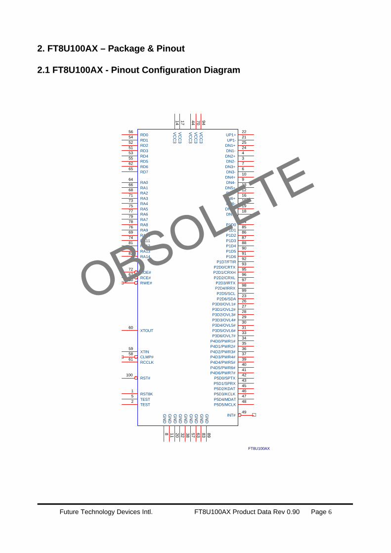
2. FT8U100AX – Package & Pinout
2.1 FT8U100AX - Pinout Configuration Diagram
FT8U100AX
RD056
RD154
RD252
RD351
RD453
RD555
RD662
RD765
RA064
RA166
RA268
RA371
RA473
RA575
RA677
RA779
RA878
RA976
RA1069
RA1174
RA1281
RA1380
RA1482
UP1+22
UP1-21
DN1+25
DN1-24
DN2+4
DN2-3
DN3+7
DN3-6
DN4+10
DN4-9
DN5+13
DN5-12
DN6+16
DN6-15
DN7+19
DN7-18
GN
D8
GN
D11
GN
D20
GN
D32
GN
D38
GN
D57
GN
D63
GN
D83
GN
D89
VC
C3
94
VC
C3
70
VC
C3
44
P1D084
P1D185
P1D286
P1D387
P1D488
P1D590
P1D691
P1D7/FTIR92
P2D0/CRTX93
P2D1/CRXH95
P2D2/CRXL96
P2D3/IRTX97
P2D4/IRRX98
P2D5/SCL99
P2D6/SDA23
P3D0/OVL1#26
P3D1/OVL2#27
P3D2/OVL3#28
P3D3/OVL4#29
P3D4/OVL5#30
P3D5/OVL6#31
P3D6/OVL7#33
P4D0/PWR1#34
P4D1/PWR2#35
P4D2/PWR3#36
P4D3/PWR4#37
P4D4/PWR5#39
P4D5/PWR6#40
P4D6/PWR7#41
P5D0/SPTX42
P5D1/SPRX43
P5D2/KDAT45
P5D3/KCLK46
P5D4/MDAT47
P5D5/MCLK48
TEST2 TEST5
RST#100
VC
C3
17
VC
C3
14
RST8K1
RWE#50 RCE#67 ROE#72
XTIN59
XTOUT60
INT#49
CLMP#58
RCCLK61
OBSOLETE

Future Technology Devices Intl. FT8U100AX Product Data Rev 0.90 Page 7
2.2 FT8U100AX - Pinout Description
PinNumber(s)
SignalName
I/O Signal Description
22,21 UP1+, UP1- USB I/O Differential USB port Connection to Upstream System or Hub25,244,37,610,913,1216,1519,18
DN1+, DN1-DN2+, DN2-DN3+, DN3-DN4+, DN4-DN5+, DN5-DN6+, DN6-DN7+, DN7-
USB I/O Differential USB port Connection to Downstream Peripherals orHubs
34-37,39,40 PWR1# toPWR7#
I/O Active Low Power Enable output pin to each USB Port. Thesesignals connect to the gate input of a Power MOSFET or PowerControl Switch I.C.
26-31,33 OVL1# toOVL7#
I/O Active Low Current Overload Detect Input from each USB Port.Pulling these signals low remove the power to the faulty USBdevice and notifies the system of this event.
84-88, 90-9293, 95-99,2326-31,3334-37,39-4142,43,45-48
P1D0 to P1D7,P2D0 to P2D6,P3D0 to P3D6,P4D0 to P4D6,P5D0 to P5D5
I/O General Purpose IO Ports used for controlling LED statusindicators etc. Some of these pins are multiplexed with otherembedded functions – see Pinout Configuration
42,43 SPTX, SPRX I/O Transmit / Receive Data for Serial Port 197,98 IRTX, IRRX I/O Transmit / Receive Data for Serial Port 2 and IrDA SIR93,96,95 CRTX,
CRXL,CRXHI/O Transmit / Receive Data for Serial Port 3 and IrDA CIR
46,45 KCLK, KDAT I/O PS/2 Keyboard interface signals48,47 MCLK, MDAT I/O PS/2 Mouse interface signals99,2349
SCL,SDAINT#
I/O Monitor Control port clock and data signals.
92 FTIR I/O Ir Remote Control Receiver Port64,66,68,71,73,75,77,79,78,76,69,74,81,80,82
RA0 to RA14 O Program Address Bus from the internal EMCU micro-controller.These connect to the address pins on an external ROM.
56,54,52,51,53,55,62,65
RD0 to RD7 I/O Program Data Bus from the internal EMCU micro-controller. Theseconnect to the address pins on an external ROM.
72,67,50 ROE#, RWE#,RCE#
O Output Enable, Write Enable and Chip Enable control signals (active low ) for the external ROM.
61 RCCLK O Oscillator Re-Start Timer RC network. This gates off the oscillatorinternal to the chip until the Oscillator circuit has become stable.
2,3 TEST I For IC Test Purpose Only – Strap to GND1 RST8K I For FTDI In-Circuit Debugger Use Only – Strap to GND for normal
operation.
58 CLMP# I Strapped to XTIN for Bus powered applications – used to shutdown the oscillator circuit during suspend by clamping the input toground.
59,60 XTIN, XTOUT I,O 48MHz Crystal Oscillator Input / Output Pins100 RST# I Active Low Chip Reset Pin14,17,44,70,94 VCC3 VCC +3.3 Volt Supply Voltage8,11,20,32,38,57,63,83,89
GND GND Ground Pin
The FT8U100AX contains six general purpose I/O ports which are firmware configurable. These support LED statuscontrol, USB overload current detect, per port USB power enable functions as well as internal legacy peripheralsincluding serial port, PS/2 keyboard and mouse. The pinout diagram on the preceding page details the designation ofthese I/O ports for one specific configuration of the FT8U100AX, as used with the UH8370 USB Hub reference design.
OBSOLETE

Future Technology Devices Intl. FT8U100AX Product Data Rev 0.90 Page 8
2.3 FT8U100AX – Package Mechanical Drawing
o
+/- 0.1020.00
23.90 +/- 0.25
14.00
+/- 0.10
17.90
+/- 0.25
#1
0.65 0.25 ~ 0.39 (0.58)
0 ~ 8o
0.65 ~ 0.95
0.10 ~ 0.36
2.87 ~ 3.18
0.13 ~ 0.203
ALL DIMENSIONS IN MILLIMETRES
OBSOLETE

Future Technology Devices Intl. FT8U100AX Product Data Rev 0.90 Page 9
3. Electrical Specifications
3.1 Absolute Maximum Ratings
Parameter Min Max UnitsStorage Temperature -65 +150 oCAmbient Temperature ( Power Applied) 0 +70 oCVCC3 Supply Voltage -0.5 +4.5 VDC Input Voltage - Inputs -0.5 VCC3+0.5 VDC Input Voltage - High Impedance Bidirectionals -0.5 VCC3+0.5 VDC Output Current – Outputs 24 mADC Output Current – Low Impedance Bidirectionals 24 mAPower Dissipation 500 mW
3.2 DC Characteristics ( Ambient Temperature = 0 .. 70 Degrees C )
Symbol Description Min Max Units ConditionsVCC3 Operating Supply Voltage 3.0 3.6 vIcc1 Operating Supply Current 50 mA Normal OperationIcc2 Operating Supply Current 250 uA USB SuspendIoh1 Digital IO Pins Source Current 6 mA Voh = VCC3 – 0.5vIol1 Digital IO Pins Sink Current 12 mA Vol = + 0.5vIoh2 Digital Output Pins Source Current 2 mA Voh = VCC3 – 0.5vIol2 Digital Output Pins Sink Current 4 mA Vol = + 0.5vVoh1 Input Voltage Threshold ( Low ) 0.6 v VDD=3.0V,
RL = 1.5K to VDDVol1 Input Voltage Threshold ( High ) 2.7 v VDD=3.0V,
RL = 1.5K to VDDVDif USB Differential Input Sensitivity 0.2 v VDD = 3.0 to 3.6VVCom USB Differential Common Mode 0.8 2.5 v VDD = 3.0 to 3.6VURxt USB Single Ended Rx Threshold 0.8 2.0 v VDD = 3.0 to 3.6VUVh USB IO Pins Static Output ( Low ) 0.3v Rl = 1.5k to 3.6vUVl USB IO Pins Static Output ( High ) 2.8 Rl = 1.5k to GNDVHYS Hysteresis on SE receiver inputs 0.1v 0.2v VDD = 3 to 3.6VVIHSE High threshold for SE receiver 1.2 1.5 1.8 VDD = 3 to 3.6VVILSE Low threshold for SE receiver 1.0 1.3 1.5 VDD = 3 to 3.6V
OBSOLETE

Future Technology Devices Intl. FT8U100AX Product Data Rev 0.90 Page 10
3.3 AC Switching Characteristics
The FT8U100AX operates off of a 48MHz input frequecy. This is divided by 4 and passed to the chip’s on boardmicrocontroller, FTDI’s EMCU, as a 12MHz input clock. The user does not have visibility of this clock however it isuseful to relate timings to this clock and as such it is inlcuded.
The key timings for the FT8U100AX relate to ROM access and reset operations.
ROM access wait states can be set from 0 to 3 wait states under the control of the Chip Control Register at addressCCh.
Program ROM data read (zero wait state)
Symbol Parameter Conditions Min Typ Max Units
TRAH Address valid fromCLK rising
VCC3 = 3.0 to 3.6V 25 nS
TRDS ROM data setup toCLK
VCC3 = 3.0 to 3.6V 10 nS
TACC ROM access time VCC3 = 3.0 to 3.6V 55 nS
The above table shows the case for a zero wait state program ROM read - where the read must take place within 80nS.This requires a ROM access time of 55nS. For One wait state operation 125nS parts can be used.
CLK12
ROMA
ROMD
TRAH
TRDS
TACC
OBSOLETE

Future Technology Devices Intl. FT8U100AX Product Data Rev 0.90 Page 11
Reset operation (zero wait states ROM read)
Symbol Parameter Conditions Min Typ Max Units
TRESET RSTIN pulse width VCC3 = 3.0 to 3.6V 16 Clk48cycles
TRS RSTIN low to ROMaddress settling
VCC3 = 3.0 to 3.6V 16 Clk48cycles
The FT8U100AX should be given a reset pulse, TRESET, of at least 16 clock cycles to ensure stability. During reset the48MHz clock signal must be stable.
TRS represents the time required for the FT8U100AX to begin stable operation after the removal of the reset pulse –and can be referenced to the setting of ROM address bit 0. This time is set at a minimum of 16 Clk48 cycles – wellwithin the USB specification’s reset recovery requirement of 10mS for Hubs to be able to accept requests after theremoval of reset.
CLK12
RSTIN
ROMA
Internal CPU startsignal
ROMD
$xxxx $S000 $S001
Don't care
TRS
TRESET
Valid Valid
OBSOLETE
Future Technology Devices Intl. FT8U100AX Product Data Rev 0.90 Page 12
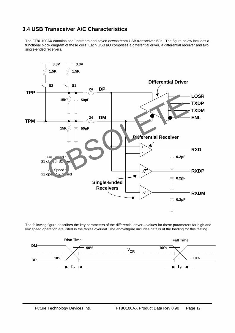
3.4 USB Transceiver A/C Characteristics
The FT8U100AX contains one upstream and seven downstream USB transceiver I/Os. The figure below includes afunctional block diagram of these cells. Each USB I/O comprises a differential driver, a differential receiver and twosingle-ended receivers.
The following figure describes the key parameters of the differential driver – values for these parameters for high andlow speed operation are listed in the tables overleaf. The abovefigure includes details of the loading for this testing.
TPM
+
-
DP
DM
RXD
RXDP
RXDM
LOSR
TXDP
TXDM
ENL
Differential Driver
Differential Receiver
Single-EndedReceivers
50pF
3.3V
1.5K
S1
3.3V
1.5K
S224
24
15K
15K 50pF
TPP
0.2pF
0.2pF
0.2pF
Full Speed :S1 closed, S2 open
Low Speed :S1 open, S2 closed
t r
10%
90%
Rise Time Fall Time
90%
10%
t f
DM
DP
VCR
OBSOLETE

Future Technology Devices Intl. FT8U100AX Product Data Rev 0.90 Page 13
Differential Driver Characteristics – High Speed
Symbol Parameter Conditions Min Typ Max Units
tr Rise time VDD = 3.0 to 3.6VCL = 50pF
8 12 nS
tf Fall time VDD = 3.0 to 3.6VCL = 50pF
8 12 nS
VCR Cross Over Voltage VDD = 3.0 to 3.6VCL = 50pF
1.8 V
trfmch Rise/Fall timematching
VDD = 3.0 to 3.6VCL = 50pF
90 110 %
Differential Driver Characteristics – Low Speed
Symbol Parameter Conditions Min Typ Max Units
tr Rise time VDD = 3.0 to 3.6VCL = 50pF
85 215 nS
tf Fall time VDD = 3.0 to 3.6VCL = 50pF
95 255 nS
VCR Cross Over Voltage VDD = 3.0 to 3.6VCL = 50pF
1.6 V
trfmch Rise/Fall timematching
VDD = 3.0 to 3.6VCL = 50pF
80 120 %
The differential receiver must exhibit input sensitivity of at least 200mV when both differential data inputs are in thedifferential common mode range of 0.8 to 2.5V as shown above. These values are shown in the DC Characteristicstable on page 9.
Differential Input Sensitivity Range
The single ended receivers are standard CMOS buffers with adjusted thresholds and which exhibit hysteresis –necessary to reduce sensitivity to noise (see VHYS on the DC Characteristcs table, page 9).
Min
imu
m D
iffe
ren
tial S
en
sit
ivit
y (
vo
lts)
Common Mode Input Voltage (volts )0.0
0.0
0.4 0.8 1.2 1.6 2.0 2.4 2.8 3.2
0.2
0.4
0.6
0.8
1.0
OBSOLETE

Future Technology Devices Intl. FT8U100AX Product Data Rev 0.90 Page 14
4. Internal IO Register Summary
The registers contained within the FT8U100AX can be described in terms of the following five main groups
USB Downstream RegistersUSB Suspend RegistersUSB Upstream RegistersUSB Device/EndPoint RegistersChip Control Registers
A summary of the function of each register group is given followed by tables detailing the register contents. Wherenecessary a short description of the function of specific registers is provided.
4.1 USB Downstream Registers
The following registers provide indexing, control and status information for up to seven USB downstream portssupported by the FT8U100AX.
This register acts as an index into the downstream port data registers - which provide control and status for even andodd indexes respectively.
USB Hub Downstream Port index registerAddress = 90h w/o
0/1 – Select Port 12/3 – Select Port 24/5 – Select Port 36/7 – Select Port 48/9 – Select Port 5A/B – Select Port 6C/D – Select Port 7
USB Hub Downstream Port Data register Address = 91h r/w
Even index – control Bit 0 – Set Power On Bit 1 – Set Port EnableBit 2 – Set Port ResetBit 3 – Set Port SuspendBit 4 – Set Power OKBit 5 – Set Reset Activity DetectBit 6 – Set Signal ResumeBit 7 – Set SE0 (set single ended zero)
odd index – status
Bit 0 - Connect DetectedBit 1 - Port EnabledBit 2 - Port SuspendedBit 3 - Port Over Current detectedBit 4 - Port ResetBit 5 - Enable Power InterruptBit 6 - NOT Full Speed DeviceBit 7 - Resume Signalled
USB Hub Downstream Port Control register Address = 92h r/w
Bit 0 - Frame timer enableBit 1 - Hub SuspendBit 2 - Signal ResumeBit 3 - Three bit window for seeing SOFBit 4 - IRQMask masks Host resume IRQBit 5 - Force EOF2 – End of Frame2 set 10 clocks before the start of frame
OBSOLETE

Future Technology Devices Intl. FT8U100AX Product Data Rev 0.90 Page 15
Bit 6 - '0'Bit 7 - Host Resume - read only
USB Hub Downstream Port Activity register Address = 93h r/o
Bit 0 - Frame Timer LockedBit 1 - Activity Detected on port 1Bit 2 - Activity Detected on port 2Bit 3 - Activity Detected on port 3Bit 4 - Activity Detected on port 4Bit 5 - Activity Detected on port 5Bit 6 - Activity Detected on port 6Bit 7 - Activity Detected on port 7
EOF2 is generated by the Frame Timer 10 clocks prior to the End Of Frame. This is provided as a local frame reference when the Host is insuspend, and EOF is not being generated. This register indicates the state of the USB lines on each downstream port at EOF2.
USB Hub Downstream Port EOF2 Data Line State register Address = 94h r/o
Bit 0 - port1 D-Bit 1 - port1 D+Bit 2 - port2 D-Bit 3 - port2 D+Bit 4 - port3 D-Bit 5 - port3 D+Bit 6 - port4 D-Bit 7 - port4 D+
USB Hub Downstream Port EOF2 Data Line State register Address = 95h r/o
Bit 0 - port5 D-Bit 1 - port5 D+Bit 2 - port6 D-Bit 3 - port6 D+Bit 4 - port7 D-Bit 5 - port7 D+Bit 6 - '0'Bit 7 - '0'
Enable PWR switch lines for I/O port muxingAddress = 96h
Bit 0 - Enable power on port1Bit 1 - Enable power on port2Bit 2 - Enable power on port3Bit 3 - Enable power on port4Bit 4 - Enable power on port5Bit 5 - Enable power on port6Bit 6 - Enable power on port7Bit 7 - Force Frame Lock
IRQ Enable for Downstream HUB PORTSAddress = 97h
Bit 0 - EN PORT 1 IRQBit 1 - EN PORT 2 IRQBit 2 - EN PORT 3 IRQBit 3 - EN PORT 4 IRQBit 4 - EN PORT 5 IRQBit 5 - EN PORT 6 IRQBit 6 - EN PORT 7 IRQ
OBSOLETE

Future Technology Devices Intl. FT8U100AX Product Data Rev 0.90 Page 16
4.2 USB Suspend Registers
The following registers provide support for suspend and resume. To clarify the terminology used asynchronousresume returns the USB from suspend when a K state on a downstream port is signalled and passed directly to theHost without the intervention of the Hub – this would be the case for example with a bus powered hub in which theclocks are stopped during suspend. Remote wakeup on the other hand requires the active intervention of the Hub.
WakeUp / Resume Control Register 2Address = 9Ch
Command register 2 :
Bit 0 - Enable asynchronous resume Bit 1 - Enable remote wakeup Bit 2 - Bit 3 - Bit 4 - Bit 5 - Bit 6 - Bit 7 -
Resume detection for async resumeAddress = 9Dh
Bit 0 - Resume on PORT 1Bit 1 - Resume on PORT 2Bit 2 - Resume on PORT 3Bit 3 - Resume on PORT 4Bit 4 - Resume on PORT 5Bit 5 - Resume on PORT 6Bit 6 - Resume on PORT 7Bit 7 -
4.3 USB Upstream Registers
The following group provides the necessary status and control registers to support the USB upstream port.
USB Main status registerAddress = A0h r/o
bit 0 - IRQ for Start of Framebit 1 - IRQ for Receiver fullbit 2 - IRQ for Transmitter emptybit 3 - Bus Idlebit 4 - Reset received from USB I/Fbit 5 -bit 6 -bit 7 - resume out detected form Host
USB Main Control registerAddress = A1h r/w
bit 0 - Reset Start Of Frame Interrupt when 0, Enable interrupt when 1bit 1 - Reset Receive Buffer Full Interrupt when 0, Enable interrupt when 1bit 2 - Reset Transmit Buffer Empty Interrupt when 0, Enable interrupt when 1bit 3 - Reset Bus Idle status bit when 0bit 4 - Clock Stop Requestbit 5 - Enable interrupt on Resumebit 6 - Force Bus to signal Resumebit 7 – Suspend In (to the SIE)
OBSOLETE

Future Technology Devices Intl. FT8U100AX Product Data Rev 0.90 Page 17
4.4 USB Device/Endpoint Registers
This group provides device and frame addresses as well as endpoint index registers. The operation of these ties inwith the explanation of the EndPoint organisation in Appendix A, part 2.
USB Device registerAddress = A2h r/w
bit 0 – Device Address 0bit 1 - Device Address 1bit 2 - Device Address 2bit 3 - Device Address 3bit 4 - Device Address 4bit 5 - Device Address 5bit 6 - Device Address 6bit 7 - '0'
USB End-Point Enable registerAddress = A3h r/w
Bit 0 - Enable for End Point 0 - no effect always enabledbit 1 - Enable for End Point 1bit 2 - Enable for End Point 2bit 3 - Enable for End Point 3bit 4 - '0'bit 5 - '0'bit 6 - '0'bit 7 - '0'
A sixty four byte buffer is available and can be switched between device 0 and device 1 under the control of bit 6 ofthe Endpoint Configuration register.
USB Device Endpoint configurationAddress = A6h w/o
bit 0 - device address bit 0bit 1 - device address bit 1bit 2 - '0'bit 3 - '0'bit 4 - Enable device 1bit 5 - Enable device 2bit 6 - 64 bytes on dev 0 = 1 /64 bytes on dev 1 = 0bit 7 - '0'
USB EndPoint Buffer Index register Address = A8h r/w
Write:bit 0 - End Point Address bit 0bit 1 - End Point Address bit 1bit 2 - Access Receive Region when 0, transmit region when 1bit 3 - Reset Receive Buffer Full when 0bit 4 - '0'bit 5 - '0'bit 6 - '0'bit 7 - '0'
Read:bit 0 - End Point Address bit 0bit 1 - End Point Address bit 1bit 2 - CPU Write to SRAM in progressbit 3 - CPU Read to SRAM in progressbit 4 - '0'bit 5 - '0'bit 6 - '0'bit 7 - '0'
OBSOLETE

Future Technology Devices Intl. FT8U100AX Product Data Rev 0.90 Page 18
USB EndPoint Status register Address = AAh r/w
Write:bit 0 -bit 1 -bit 2 - End Point Stalledbit 3 -bit 4 - Data 0 when 0, Data 1 when 1bit 5 -bit 6 -bit 7 -
Read:bit 0 - ACK for last transmitbit 1 - Error for last transferbit 2 - ACK for last receivebit 3 - Setup packetbit 4 - Data 0 when 0, Data 1 when 1bit 5 - Receive Buffer Fullbit 6 - Transmit Buffer Emptybit 7 - Transmit Direction: 0 = out(to us) 1 = in (from us)
USB EndPoint Buffer data register Address = ABh r/w
Bit 0 – EP Buffer data Bit 0Bit 1 – EP Buffer data Bit 1Bit 2 – EP Buffer data Bit 2Bit 3 – EP Buffer data Bit 3Bit 4 – EP Buffer data Bit 4Bit 5 – EP Buffer data Bit 5Bit 6 – EP Buffer data Bit 6Bit 7 – EP Buffer data Bit 7
USB EndPoint Buffer Count Low register Address = ACh r/wRead: read low 8 bits of RX countWrite: write low 8 bits of TX countWriting low count register sets the TXFULL in bit for that end point.
Bit 0 – EP Buffer count Bit 0Bit 1 – EP Buffer count Bit 1Bit 2 – EP Buffer count Bit 2Bit 3 – EP Buffer count Bit 3Bit 4 – EP Buffer count Bit 4Bit 5 – EP Buffer count Bit 5Bit 6 – EP Buffer count Bit 6Bit 7 – EP Buffer count Bit 7
USB EndPoint Buffer CPU Count Low register Address = AEh r/wRead: read low 8 bits of RX countWrite: write low 8 bits of TX countWriting low count register sets the TXFULL in bit for that end point.
Bit 0 – EP Buffer count Bit 0Bit 1 – EP Buffer count Bit 1Bit 2 – EP Buffer count Bit 2Bit 3 – EP Buffer count Bit 3Bit 4 – EP Buffer count Bit 4Bit 5 – EP Buffer count Bit 5Bit 6 – EP Buffer count Bit 6Bit 7 – EP Buffer count Bit 7
OBSOLETE

Future Technology Devices Intl. FT8U100AX Product Data Rev 0.90 Page 19
4.5 Chip Control Registers
This group provides on chip interrupt support (timer count, control and prescaler), internal peripheral controlregisters, in circuit debugger support registers, IRQ source register and support registers for PS/2 keyboard andmouse functions.
Interrupt Timer – Count LowAddress = B1h r/w
Bit 0 – Timer count Bit 0Bit 1 – Timer count Bit 1Bit 2 – Timer count Bit 2Bit 3 – Timer count Bit 3Bit 4 – Timer count Bit 4Bit 5 – Timer count Bit 5Bit 6 – Timer count Bit 6Bit 7 – Timer count Bit 7
Interrupt Timer – Count HighAddress = B2h r/w
Bit 0 – Timer count Bit 8Bit 1 – Timer count Bit 9Bit 2 – Timer count Bit10Bit 3 – Timer count Bit 11Bit 4 – Timer count Bit 12Bit 5 – Timer count Bit 13Bit 6 – Timer count Bit 14Bit 7 – Timer count Bit 15
Interrupt Timer – Prescaler DivisorAddress = B8h r/w
Bit 0 – Prescaler Divisor Bit 0Bit 1 – Prescaler Divisor Bit 1Bit 2 – Prescaler Divisor Bit 2Bit 3 – Prescaler Divisor Bit 3Bit 4 – Prescaler Divisor Bit 4Bit 5 – Prescaler Divisor Bit 5Bit 6 – Prescaler Divisor Bit 6Bit 7 – Prescaler Divisor Bit 7
CHIP CONTROL Register – LowAddress = CCh w/o
Bit 0 - Enable serial port interrupt on DEBUG interrupt – to speed up operationBit 1 - Force No Operation code on ROM dataBit 2 - Force internal Memory Address bus to appear on I/O portsBit 3 – 7
CHIP CONTROL Register – HighAddress = CCh w/o
Bit 0 Enable serial portBit 1 Enable PS2 mouseBit 2 Enable hub functionBit 3 Enable SIEBit 4 Enable on chip timerBit 5 Enable PS2 keyboardBit 6 ROM wait state 0, bits 6 and 7 encode the number of ROM wait states (0 to 3)Bit 7 ROM wait state 1
OBSOLETE
Future Technology Devices Intl. FT8U100AX Product Data Rev 0.90 Page 20
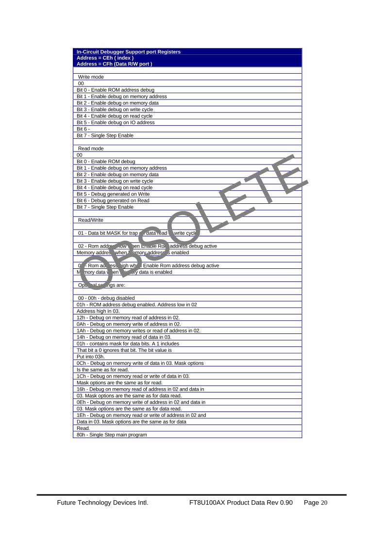
In-Circuit Debugger Support port RegistersAddress = CEh ( index )Address = CFh (Data R/W port )
Write mode 00Bit 0 - Enable ROM address debugBit 1 - Enable debug on memory addressBit 2 - Enable debug on memory dataBit 3 - Enable debug on write cycleBit 4 - Enable debug on read cycleBit 5 - Enable debug on IO addressBit 6 -Bit 7 - Single Step Enable
Read mode00Bit 0 - Enable ROM debugBit 1 - Enable debug on memory addressBit 2 - Enable debug on memory dataBit 3 - Enable debug on write cycleBit 4 - Enable debug on read cycleBit 5 - Debug generated on WriteBit 6 - Debug generated on ReadBit 7 - Single Step Enable
Read/Write
01 - Data bit MASK for trap on data read or write cycles
02 - Rom address low when Enable Rom address debug activeMemory address when Memory address is enabled
03 - Rom address high when Enable Rom address debug activeMemory data when Memory data is enabled
Optional settings are:
00 - 00h - debug disabled01h - ROM address debug enabled. Address low in 02Address high in 03.12h - Debug on memory read of address in 02.0Ah - Debug on memory write of address in 02.1Ah - Debug on memory writes or read of address in 02.14h - Debug on memory read of data in 03.01h - contains mask for data bits. A 1 includesThat bit a 0 ignores that bit. The bit value isPut into 03h.0Ch - Debug on memory write of data in 03. Mask optionsIs the same as for read.1Ch - Debug on memory read or write of data in 03.Mask options are the same as for read.16h - Debug on memory read of address in 02 and data in03. Mask options are the same as for data read.0Eh - Debug on memory write of address in 02 and data in03. Mask options are the same as for data read.1Eh - Debug on memory read or write of address in 02 andData in 03. Mask options are the same as for dataRead.80h - Single Step main program
OBSOLETE
Future Technology Devices Intl. FT8U100AX Product Data Rev 0.90 Page 21
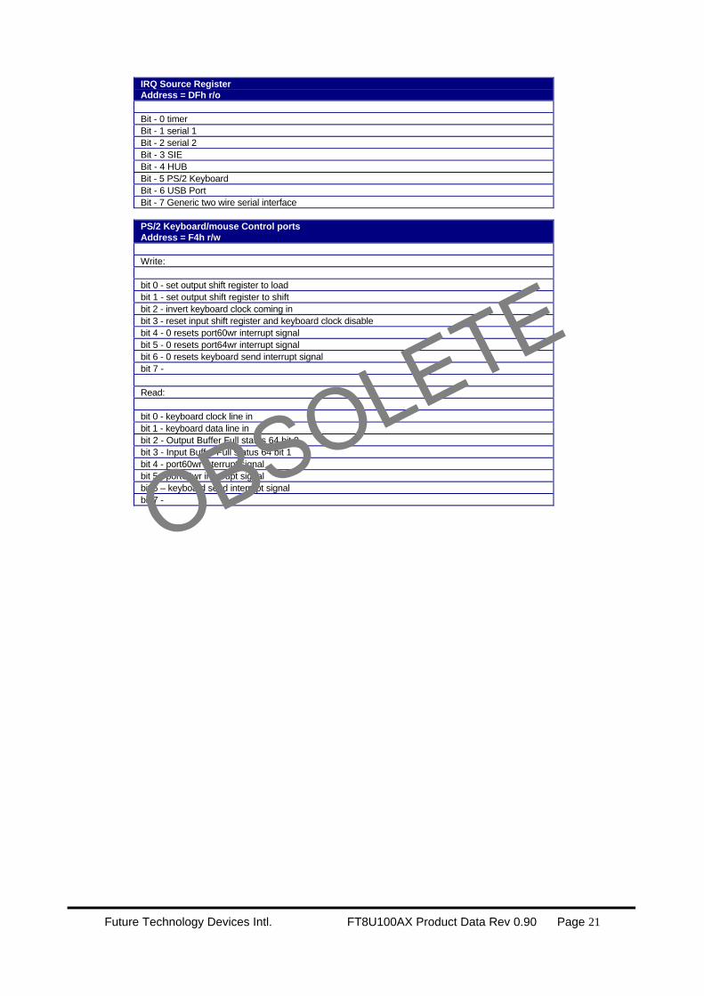
IRQ Source RegisterAddress = DFh r/o
Bit - 0 timerBit - 1 serial 1Bit - 2 serial 2Bit - 3 SIEBit - 4 HUBBit - 5 PS/2 KeyboardBit - 6 USB PortBit - 7 Generic two wire serial interface
PS/2 Keyboard/mouse Control portsAddress = F4h r/w
Write:
bit 0 - set output shift register to loadbit 1 - set output shift register to shiftbit 2 - invert keyboard clock coming inbit 3 - reset input shift register and keyboard clock disablebit 4 - 0 resets port60wr interrupt signalbit 5 - 0 resets port64wr interrupt signalbit 6 - 0 resets keyboard send interrupt signalbit 7 -
Read:
bit 0 - keyboard clock line inbit 1 - keyboard data line inbit 2 - Output Buffer Full status 64 bit 0bit 3 - Input Buffer Full status 64 bit 1bit 4 - port60wr interrupt signalbit 5 - port64wr interrupt signalbit 6 – keyboard send interrupt signalbit 7 -OBSOLETE
Future Technology Devices Intl. FT8U100AX Product Data Rev 0.90 Page 22
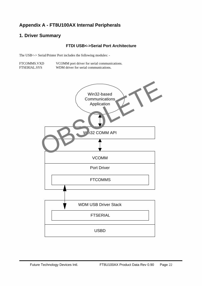
Appendix A - FT8U100AX Internal Peripherals
1. Driver Summary
FTDI USB<->Serial Port Architecture
The USB<-> Serial/Printer Port includes the following modules: -
FTCOMMS.VXD VCOMM port driver for serial communications.FTSERIAL.SYS WDM driver for serial communications.
Win32 COMM API
VCOMM
Port Driver
USBD
Win32-basedCommunications
Application
FTCOMMS
FTSERIAL
WDM USB Driver Stack
OBSOLETE
Future Technology Devices Intl. FT8U100AX Product Data Rev 0.90 Page 23
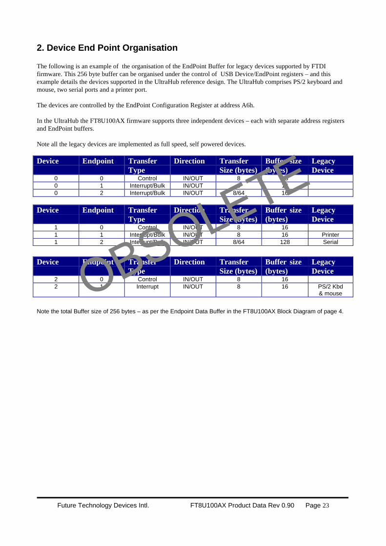
2. Device End Point Organisation
The following is an example of the organisation of the EndPoint Buffer for legacy devices supported by FTDIfirmware. This 256 byte buffer can be organised under the control of USB Device/EndPoint registers – and thisexample details the devices supported in the UltraHub reference design. The UltraHub comprises PS/2 keyboard andmouse, two serial ports and a printer port.
The devices are controlled by the EndPoint Configuration Register at address A6h.
In the UltraHub the FT8U100AX firmware supports three independent devices – each with separate address registersand EndPoint buffers.
Note all the legacy devices are implemented as full speed, self powered devices.
Device Endpoint TransferType
Direction TransferSize (bytes)
Buffer size (bytes)
LegacyDevice
0 0 Control IN/OUT 8 160 1 Interrupt/Bulk IN/OUT 8 160 2 Interrupt/Bulk IN/OUT 8/64 16
Device Endpoint TransferType
Direction TransferSize (bytes)
Buffer size (bytes)
LegacyDevice
1 0 Control IN/OUT 8 161 1 Interrupt/Bulk IN/OUT 8 16 Printer1 2 Interrupt/Bulk IN/OUT 8/64 128 Serial
Device Endpoint TransferType
Direction TransferSize (bytes)
Buffer size (bytes)
LegacyDevice
2 0 Control IN/OUT 8 162 1 Interrupt IN/OUT 8 16 PS/2 Kbd
& mouse
Note the total Buffer size of 256 bytes – as per the Endpoint Data Buffer in the FT8U100AX Block Diagram of page 4.
OBSOLETE
Future Technology Devices Intl. FT8U100AX Product Data Rev 0.90 Page 24
3. USB and Legacy Device LED Encoding
The FT8U100AX supports powerful LED-based diagnostic and status features. This provides useful information in anenvironment where failure isolation can be difficult. FTDI standard firmware supports two LEDs (one yellow, one green)per USB port – in a configuration shown on page 4 of the UltraHub application schematic.
In addition to the USB port LEDs the FT8U100AX supports traffic indicator LEDs for legacy devices. These areswitched on when individual legacy devices are configured and flash when there is Bus Traffic from the appropriatedevice.
The following describes the operation of the LEDs under normal conditions as well as suggesting a basic sequence ofsteps for locating the likely source of any problems which may be encountered.
On power up
1) All Lights On - hub has been properly reset. LEDs will light up for a short period indicating that the hub has beenproperly initialised.
2) All Lights Off - USB has enumerated the hub. This indicates that the hub has been succesfully initialised by USB.
On plugging a USB peripheral into a port
3A) Yellow On - LOW Speed USB Peripheral plugged into hub, followed quickly by
4A) Yellow On and Green Twinkles - Bus Traffic from LOW Speed Peripheral connected to hub, OR
3B) Green On - HIGH Speed USB Peripheral plugged into hub, followed quickly by
4B) Green On and Yellow Twinkles - Bus Traffic from HIGH Speed Peripheral connected to hub.
In addition the LEDs indicate specific USB conditions including: USB reset – both LEDs come on continuously andUSB suspend – both LEDs go off continuously.
Error conditions
If the lights do not come on when a peripheral is plugged in, the peripheral has not been detected by the USB. Noticethat this is different from the USB suspend condition where the peripheral is already functional when the LEDs go off.
Both Green and Yellow Twinkle in Phase - Overcurrent Error Condition. Peripheral has taken too much current and thehub has shut off power to the peripheral.
Both Green and Yellow Twinkle in AntiPhase - Babble Error Condition. Peripheral continues sending data at the end ofthe USB 1ms Frame interval and the hub has shut off the bus traffic from the peripheral.
Problem Diagnosis - follow this procedure to identify if problem is due to upstream device, hub or downstream device
Step 1) Remove all USB cables (upstream and downstream), leaving only the power cable connected to hub. Switchhub power on. All LEDs should go on as described in 1) on the previous page. If all LEDs go on proceed to step 2. If allthe LEDs do not come there may well be a problem with the hub or its power supply.
Step 2) Plug in the upstream USB cable (connected to an upstream device - the system box or another hub). The LEDsshould all go out. If all LEDs go off proceed to step 3. If the LEDs do not go out the hub has not been correctlyenumerated by the USB. This can be a problem with the upstream device or with the hub.
Replace you hub with a USB peripheral (or another hub if available) to check that the upstream device is functional. Ifthis fails then you may have problem with an upstream hub or with the system box. If this device functions as expectedthen the hub will need further investigation.
Step 3) If there are no problems with steps 1 and 2 then begin testing you downstream devices by plugging them intothe hub one at a time. The LEDs should behave as described in 3) and 4) on the previous page.
If you have a problem with a downstream device try plugging it into another port - in case there is a problem with oneport. If you have already found a good device you will have some confidence that the port it used is functioning. If theproblem device continues to fail in this port then it is likely that this device is the source of the problem.
OBSOLETE

Future Technology Devices Intl. FT8U100AX Product Data Rev 0.90 Page 25
Disclaimer & Contact Information
© Future Technology Devices International Limited – 1996…2000
Neither the whole nor any part of the information contained in, or the product described in this manual, may be adapted
or reproduced in any material or electronic form without the prior written consent of the copyright holder.
This product and its documentation are supplied on an as is basis and no warranty as to their suitability for any
particular purpose is either made or implied. Future Technology Devices will not accept any claim for damages
howsoever arising as a result of use or failure of this product. Your statutory rights are not affected.
This product or any variant of it is not intended for use in any medical appliance, device or system in which the failure
of the product might reasonably be expected to result in personal injury.
This document provides preliminary information that may be subject to change without notice.
Contact Information
Future Technology Devices International has agents and distributors based in Europe, the US and throughout
the Far East. For further information and to obtain local contact details please contact us, preferably by e-mail,
at the address below.
Future Technology Devices Intl Limited Telephone : +44 (141) 353 2565
St. George’s Studios Fax : +44 (141) 353 2656
93/97 St. George’s Road E-mail : [email protected]
Glasgow G3 6JA, UK Internet : http://www.ftdi.co.ukOBSOLETE