
CARTA ESCRITA EN EL 2070 www ww w www wW w w ww w w w w ww w w w www w W w w ww w w w ww w .
Upload
abdul-quddosCategory
view
310download
10description


Frontiers in Antennas: Next Generation
Design & Engineering
Frank B. Gross, PhD, Editor-in-Chief
New York Chicago San Francisco Lisbon London Madrid Mexico City
Milan New Delhi San Juan Seoul Singapore Sydney Toronto

Copyright © 2011 by The McGraw-Hill Companies. All rights reserved. Except as permitted under the United States Copyright Act of 1976, no part of this publication may be reproduced or distributed in any form or by any means, or stored in a database or retrieval system, without the prior written permission of the publisher.
ISBN: 978-0-07-163794-7
MHID: 0-07-163794-X
The material in this eBook also appears in the print version of this title: ISBN: 978-0-07-163793-0, MHID: 0-07-163793-1.
All trademarks are trademarks of their respective owners. Rather than put a trademark symbol after every occurrence of a trademarked name, we use names in an editorial fashion only, and to the benefi t of the trademark owner, with no intention of infringement of the trademark. Where such designations appear in this book, they have been printed with initial caps.
McGraw-Hill eBooks are available at special quantity discounts to use as premiums and sales promotions, or for use in corporate training programs. To contact a representative please e-mail us at [email protected].
Information has been obtained by McGraw-Hill from sources believed to be reliable. However, because of the possibility of human or mechanical error by our sources, McGraw-Hill, or others, McGraw-Hill does not guarantee the accuracy, adequacy, or completeness of any information and is not responsible for any errors or omissions or the results obtained from the use of such information.
TERMS OF USE
This is a copyrighted work and The McGraw-Hill Companies, Inc. (“McGrawHill”) and its licensors reserve all rights in and to the work. Use of this work is subject to these terms. Except as permitted under the Copyright Act of 1976 and the right to store and retrieve one copy of the work, you may not decompile, disassemble, reverse engineer, reproduce, modify, create derivative works based upon, transmit, distribute, disseminate, sell, publish or sublicense the work or any part of it without McGraw-Hill’s prior consent. You may use the work for your own noncommercial and personal use; any other use of the work is strictly prohibited. Your right to use the work may be terminated if you fail to comply with these terms.
THE WORK IS PROVIDED “AS IS.” McGRAW-HILL AND ITS LICENSORS MAKE NO GUARANTEES OR WARRANTIES AS TO THE ACCURACY, ADEQUACY OR COMPLETENESS OF OR RESULTS TO BE OBTAINED FROM USING THE WORK, INCLUDING ANY INFORMATION THAT CAN BE ACCESSED THROUGH THE WORK VIA HYPERLINK OR OTHERWISE, AND EXPRESSLY DISCLAIM ANY WARRANTY, EXPRESS OR IMPLIED, INCLUDING BUT NOT LIMITED TO IMPLIED WARRANTIES OF MERCHANTABILITY OR FITNESS FOR A PARTICULAR PURPOSE. McGraw-Hill and its licensors do not warrant or guarantee that the functions contained in the work will meet your requirements or that its operation will be uninterrupted or error free. Neither McGraw-Hill nor its licensors shall be liable to you or anyone else for any inaccuracy, error or omission, regardless of cause, in the work or for any damages resulting therefrom. McGraw-Hill has no responsibility for the content of any information accessed through the work. Under no circumstances shall McGraw-Hill and/or its licensors be liable for any indirect, incidental, special, punitive, consequential or similar damages that result from the use of or inability to use the work, even if any of them has been advised of the possibility of such damages. This limitation of liability shall apply to any claim or cause whatsoever whether such claim or cause arises in contract, tort or otherwise.

In loving memory of my father Dr. Frank Blackburn Gross Jr.
and my mother Ann Kanoy Gross

About the EditorFrank B. Gross is a Senior Scientist at Argon ST currently working in the areas of smart antennas, antenna design, direction finding, metamaterials, and propagation. He obtained his PhD from The Ohio State University in 1982. Subsequently, he became a professor at The Florida State University teaching and performing research in the areas of electromagnetics, antennas, electrostatics, smart antennas, and radar. He received the Tau Beta Pi “Best Teacher of the Year Award” and the University Teaching Incentive (TIP) award. After serving 18 years as a professor, Dr. Gross departed academia and entered into industry. He formerly has worked as a Senior Research Engineer at The Georgia Tech Research Institute (GTRI), a Lead Engineer at The MITRE Corporation, and a Chief Scientist at SAIC.
Dr. Gross has written a chapter on Bessel Functions in The Encyclopedia of Electrical and Electronics Engineering (Wiley, 1998), the book Smart Antennas for Wireless Communications with MATLAB (McGraw-Hill, 2005), and a chapter on Smart Antennas in the Antenna Engineering Handbook (McGraw-Hill, 2007). He has published numerous journal and conference articles on the topics of radar waveform design, radar scattering and imaging, frequency selective surfaces (FSS), Martian electrostatics, Bessel function approximations, and smart antennas.
v

ContentsForeword . . . . . . . . . . . . . . . . . . . . . . . . . . . . . . . . . . . . . . . . . . . . . . . . . . . xiiiPreface . . . . . . . . . . . . . . . . . . . . . . . . . . . . . . . . . . . . . . . . . . . . . . . . . . . . . xvAcknowledgments . . . . . . . . . . . . . . . . . . . . . . . . . . . . . . . . . . . . . . . . . . . xvii
1 Ultra-Wideband Antenna Arrays . . . . . . . . . . . . . . . . . . . . . . . . . . . . . . 11.1 Introduction . . . . . . . . . . . . . . . . . . . . . . . . . . . . . . . . . . . . . . . . . . . . 1
1.1.1 Grating Lobes in Periodic Arrays . . . . . . . . . . . . . . . . . . . 21.1.2 Dense Wideband Antenna Arrays . . . . . . . . . . . . . . . . . . 51.1.3 Early Aperiodic Design Methods . . . . . . . . . . . . . . . . . . . 6
1.2 Foundations of Multiband and UWB Array Design . . . . . . . . . . 71.2.1 Fractal Theory and Its Applications
to Antenna Array Design . . . . . . . . . . . . . . . . . . . . . . . 81.2.2 Aperiodic Tiling Theory . . . . . . . . . . . . . . . . . . . . . . . . . . 181.2.3 Optimization Techniques . . . . . . . . . . . . . . . . . . . . . . . . . 24
1.3 Modern UWB Array Design Techniques . . . . . . . . . . . . . . . . . . . . 271.3.1 Polyfractal Arrays . . . . . . . . . . . . . . . . . . . . . . . . . . . . . . . . 271.3.2 Arrays Based on Raised-Power
Series Representations . . . . . . . . . . . . . . . . . . . . . . . . . 291.3.3 Arrays Based on Aperiodic Tilings . . . . . . . . . . . . . . . . . 31
1.4 UWB Array Design Examples . . . . . . . . . . . . . . . . . . . . . . . . . . . . . 401.4.1 Linear and Planar Polyfractal Array Examples . . . . . . . 401.4.2 Linear RPS Array Design Examples . . . . . . . . . . . . . . . . 471.4.3 Planar Array Examples Based on Aperiodic Tilings . . . . 531.4.4 Volumetric Array Based on a 3D Aperiodic Tiling . . . . 59
1.5 Full-Wave and Experimental Verification of UWB Designs . . . . . . . . . . . . . . . . . . . . . . . . . . . . . . . . . . . . . . . . . . 61
1.5.1 Full-Wave Simulation of a Moderately Sized Optimized RPS Array . . . . . . . . . . . . . . . . . . . . . 62
1.5.2 Full-Wave Simulation of a Planar Optimized Aperiodic Tiling Array . . . . . . . . . . . . . . . . . . . . . . . . . 65
1.5.3 Experimental Verification of Two Linear Polyfractal Arrays . . . . . . . . . . . . . . . . . . . . . . . 68
References . . . . . . . . . . . . . . . . . . . . . . . . . . . . . . . . . . . . . . . . . . . . . . . . . . 72
2 Smart Antennas . . . . . . . . . . . . . . . . . . . . . . . . . . . . . . . . . . . . . . . . . . . . . 772.1 Introduction . . . . . . . . . . . . . . . . . . . . . . . . . . . . . . . . . . . . . . . . . . . . 772.2 Background on Smart Antennas . . . . . . . . . . . . . . . . . . . . . . . . . . . 79
2.2.1 Beamforming . . . . . . . . . . . . . . . . . . . . . . . . . . . . . . . . . . . . 792.2.2 Direction-of-Arrival Estimation Techniques . . . . . . . . . 83
v

vi F r o n t i e r s i n A n t e n n a s : N e x t G e n e r a t i o n D e s i g n & E n g i n e e r i n g C o n t e n t s vii
2.3 Evolutionary Signal Processing for Smart Antennas . . . . . . . . . . 862.3.1 Description of Algorithms . . . . . . . . . . . . . . . . . . . . . . . . . 892.3.2 Adaptive Beamforming and
Nulling in Smart Antennas . . . . . . . . . . . . . . . . . . . . . 962.3.3 Extensions to Algorithms for
Smart Antenna Implementation . . . . . . . . . . . . . . . . . 1022.4 Wideband Direction-of-Arrival Estimation . . . . . . . . . . . . . . . . . . 104
2.4.1 Test of Orthogonality of Projected Subspaces (TOPS) . . . . . . . . . . . . . . . . . . . . . 107
2.4.2 Test of Orthogonality of Frequency Subspaces (TOFS) . . . . . . . . . . . . . . . . . . . . 109
2.4.3 Improvements to TOPS . . . . . . . . . . . . . . . . . . . . . . . . . . . 1092.5 Knowledge Aided Smart Antennas . . . . . . . . . . . . . . . . . . . . . . . . 111
2.5.1 Terrain Information . . . . . . . . . . . . . . . . . . . . . . . . . . . . . . 1112.5.2 Analysis Tools . . . . . . . . . . . . . . . . . . . . . . . . . . . . . . . . . . . 114
2.6 Conclusion . . . . . . . . . . . . . . . . . . . . . . . . . . . . . . . . . . . . . . . . . . . . . 124Acknowledgments . . . . . . . . . . . . . . . . . . . . . . . . . . . . . . . . . . . . . 125
References . . . . . . . . . . . . . . . . . . . . . . . . . . . . . . . . . . . . . . . . . . . . . . . . . . 125
3 Vivaldi Antenna Arrays . . . . . . . . . . . . . . . . . . . . . . . . . . . . . . . . . . . . . . 1273.1 Background and General Characteristics . . . . . . . . . . . . . . . . . . . . 127
3.1.1 Introduction . . . . . . . . . . . . . . . . . . . . . . . . . . . . . . . . . . . . . 1273.1.2 Background . . . . . . . . . . . . . . . . . . . . . . . . . . . . . . . . . . . . . 1283.1.3 Applications . . . . . . . . . . . . . . . . . . . . . . . . . . . . . . . . . . . . 1283.1.4 Physical and Mechanical Description . . . . . . . . . . . . . . . 1293.1.5 Fabrication . . . . . . . . . . . . . . . . . . . . . . . . . . . . . . . . . . . . . . 1333.1.6 General Discussion of Vivaldi Array Performance . . . . 136
3.2 Design of Vivaldi Arrays . . . . . . . . . . . . . . . . . . . . . . . . . . . . . . . . . 1403.2.1 Background . . . . . . . . . . . . . . . . . . . . . . . . . . . . . . . . . . . . . 1403.2.2 Infinite Array Element Design
for Wide Bandwidth . . . . . . . . . . . . . . . . . . . . . . . . . . . 1433.2.3 Infinite × Finite Array Truncation Effects . . . . . . . . . . . . 1523.2.4 Finite Array Truncation Effects . . . . . . . . . . . . . . . . . . . . . 156
Acknowledgments . . . . . . . . . . . . . . . . . . . . . . . . . . . . . . . . . . . . . . . . . . . 165References . . . . . . . . . . . . . . . . . . . . . . . . . . . . . . . . . . . . . . . . . . . . . . . . . . 166
4 Artificial Magnetic Conductors/High-Impedance Surfaces . . . . . . . 1694.1 Introduction . . . . . . . . . . . . . . . . . . . . . . . . . . . . . . . . . . . . . . . . . . . . 1694.2 Historical Background . . . . . . . . . . . . . . . . . . . . . . . . . . . . . . . . . . . 1704.3 Fundamental Theory, Analysis, and Simulation . . . . . . . . . . . . . . 171
4.3.1 Equivalent Circuit Model . . . . . . . . . . . . . . . . . . . . . . . . . 1714.3.2 Effective Media Model . . . . . . . . . . . . . . . . . . . . . . . . . . . . 1734.3.3 CEM Simulation of AMC Structures . . . . . . . . . . . . . . . . 175
4.4 New Technologies and Applications . . . . . . . . . . . . . . . . . . . . . . . 1774.4.1 Magnetically Loaded AMC . . . . . . . . . . . . . . . . . . . . . . . . 1774.4.2 Reconfigurable AMC . . . . . . . . . . . . . . . . . . . . . . . . . . . . . 1854.4.3 Novel AMC Constructs . . . . . . . . . . . . . . . . . . . . . . . . . . . 190
References . . . . . . . . . . . . . . . . . . . . . . . . . . . . . . . . . . . . . . . . . . . . . . . . . . 198

vi F r o n t i e r s i n A n t e n n a s : N e x t G e n e r a t i o n D e s i g n & E n g i n e e r i n g C o n t e n t s vii
5 Metamaterial Antennas . . . . . . . . . . . . . . . . . . . . . . . . . . . . . . . . . . . . . . 2035.1 Introduction . . . . . . . . . . . . . . . . . . . . . . . . . . . . . . . . . . . . . . . . . . . . 2035.2 Negative Refractive Index (NRI) Metamaterials . . . . . . . . . . . . . 2045.3 Metamaterial Antennas Based on NRI Concepts . . . . . . . . . . . . . 207
5.3.1 Leaky-Wave Antennas (LWAs) . . . . . . . . . . . . . . . . . . . . . 2075.3.2 Miniature and Multiband Patch Antennas . . . . . . . . . . . 2085.3.3 Compact and Low-Profile Monopole Antennas . . . . . . 212
5.4 High-Gain Antennas Utilizing EBG Defect Modes . . . . . . . . . . . 2165.5 Antenna Miniaturization Using Dispersion
Properties of Layered Anisotropic Media . . . . . . . . . . . . . . . . . 2185.5.1 Realizing DBE and MPC Modes via
Printed Circuit Emulation of Anisotropy . . . . . . . . . . . 2205.5.2 DBE Antenna Design Using
Printed Coupled Loops . . . . . . . . . . . . . . . . . . . . . . . . . 2225.5.3 Improving DBE Antenna Performance:
Coupled Double-Loop (CDL) Antenna . . . . . . . . . . . 2255.5.4 Varactor Diode Loaded CDL Antenna . . . . . . . . . . . . . . 2275.5.5 Microstrip MPC Antenna Design . . . . . . . . . . . . . . . . . . . 228
5.6 Platform/Vehicle Integration of Metamaterial Antennas (Irci, Sertel, Volakis) . . . . . . . . . . . . . . . . . . . . . . . . . . . 228
5.7 Wideband Metamaterial Antenna Arrays (Tzanidis, Sertel, Volakis) . . . . . . . . . . . . . . . . . . . . . . . . . . . . . . . 231
5.7.1 What Are Metamaterial Antenna Arrays? . . . . . . . . . . . 2315.7.2 Schematic Representation of a Metamaterial Array . . . . 2335.7.3 An MTM Interweaved Spiral Array with 10:1 BW . . . . 234
References . . . . . . . . . . . . . . . . . . . . . . . . . . . . . . . . . . . . . . . . . . . . . . . . . . 236
6 Biological Antenna Design Methods . . . . . . . . . . . . . . . . . . . . . . . . . . 2416.1 Introduction . . . . . . . . . . . . . . . . . . . . . . . . . . . . . . . . . . . . . . . . . . . . 2416.2 Genetic Algorithm . . . . . . . . . . . . . . . . . . . . . . . . . . . . . . . . . . . . . . . 241
6.2.1 Components of a Genetic Algorithm . . . . . . . . . . . . . . . . 2426.2.2 Successful GA Strategies . . . . . . . . . . . . . . . . . . . . . . . . . . 2506.2.3 Examples . . . . . . . . . . . . . . . . . . . . . . . . . . . . . . . . . . . . . . . 252
6.3 Genetic Programming . . . . . . . . . . . . . . . . . . . . . . . . . . . . . . . . . . . . 2586.4 Efficient Global Optimization . . . . . . . . . . . . . . . . . . . . . . . . . . . . . 260
6.4.1 The DACE Stochastic Process Model . . . . . . . . . . . . . . . 2616.4.2 Estimation of the Correlation Parameters . . . . . . . . . . . . 2626.4.3 Selecting the Next Design Point . . . . . . . . . . . . . . . . . . . 2636.4.4 Convergence . . . . . . . . . . . . . . . . . . . . . . . . . . . . . . . . . . . . 2646.4.5 Comparison of EGO and GA Design Optimization . . . 264
6.5 Particle Swarm Optimization . . . . . . . . . . . . . . . . . . . . . . . . . . . . . 2646.6 Ant Colony Optimization . . . . . . . . . . . . . . . . . . . . . . . . . . . . . . . . . 266References . . . . . . . . . . . . . . . . . . . . . . . . . . . . . . . . . . . . . . . . . . . . . . . . . . 267
7 Reconfigurable Antennas . . . . . . . . . . . . . . . . . . . . . . . . . . . . . . . . . . . . . 2717.1 Introduction . . . . . . . . . . . . . . . . . . . . . . . . . . . . . . . . . . . . . . . . . . . . 271
7.1.1 Physical Components of a Reconfigurable Antenna . . . . 272

viii F r o n t i e r s i n A n t e n n a s : N e x t G e n e r a t i o n D e s i g n & E n g i n e e r i n g C o n t e n t s ix
7.1.2 Qualitative Description . . . . . . . . . . . . . . . . . . . . . . . . . . . 2737.1.3 Topology . . . . . . . . . . . . . . . . . . . . . . . . . . . . . . . . . . . . . . . 275
7.2 Analysis . . . . . . . . . . . . . . . . . . . . . . . . . . . . . . . . . . . . . . . . . . . . . . . . 2767.2.1 Transmission Line, Network, and Circuit Models . . . . . 2767.2.2 Perturbational Techniques . . . . . . . . . . . . . . . . . . . . . . . . . 2777.2.3 Variational Techniques . . . . . . . . . . . . . . . . . . . . . . . . . . . 277
7.3 Overview of Reconfiguration Mechanisms for Antennas . . . . . . 2777.3.1 Electromechanical . . . . . . . . . . . . . . . . . . . . . . . . . . . . . . . . 2777.3.2 Ferroic Materials . . . . . . . . . . . . . . . . . . . . . . . . . . . . . . . . . 2887.3.3 Solid State Mechanisms . . . . . . . . . . . . . . . . . . . . . . . . . . . 2907.3.4 Fluidic Reconfiguration . . . . . . . . . . . . . . . . . . . . . . . . . . . 2947.3.5 Switching Speeds and Other Parameters . . . . . . . . . . . . 296
7.4 Control, Automation, and Applications . . . . . . . . . . . . . . . . . . . . . 2977.5 Review . . . . . . . . . . . . . . . . . . . . . . . . . . . . . . . . . . . . . . . . . . . . . . . . . 3017.6 Final Remarks . . . . . . . . . . . . . . . . . . . . . . . . . . . . . . . . . . . . . . . . . . 301References . . . . . . . . . . . . . . . . . . . . . . . . . . . . . . . . . . . . . . . . . . . . . . . . . . 302
8 Antennas in Medicine: Ingestible Capsule Antennas . . . . . . . . . . . . 3058.1 Introduction . . . . . . . . . . . . . . . . . . . . . . . . . . . . . . . . . . . . . . . . . . . . 3058.2 Planar Meandered Dipoles . . . . . . . . . . . . . . . . . . . . . . . . . . . . . . . . 308
8.2.1 Balanced Planar Meandered Dipoles—Theory . . . . . . . 3098.2.2 Balanced Planar Meandered Dipoles—
Simulation and Measurement . . . . . . . . . . . . . . . . . . . 3118.2.3 Offset Planar Meandered Dipoles—
Simulation and Measurement . . . . . . . . . . . . . . . . . . . 3128.3 Antenna Design in Free Space . . . . . . . . . . . . . . . . . . . . . . . . . . . . . 315
8.3.1 Conformal Chandelier Meandered Dipole Antenna . . . . . 3158.4 Antenna Design in the Human Body . . . . . . . . . . . . . . . . . . . . . . . 322
8.4.1 Tuned Antenna for the Human Body . . . . . . . . . . . . . . . 3228.4.2 Effect of Electrical Components
on the Antenna Performance . . . . . . . . . . . . . . . . . . . . 3238.5 SAR Analysis and Link Budget Analysis . . . . . . . . . . . . . . . . . . . . 326
8.5.1 Simple Human-Body Model . . . . . . . . . . . . . . . . . . . . . . . 3268.5.2 Specific Absorption Rate Analysis . . . . . . . . . . . . . . . . . . 3278.5.3 Link Budget Characterization . . . . . . . . . . . . . . . . . . . . . . 3288.5.4 Link Budget for Free Space—Friis vs. HFSS . . . . . . . . . . 3308.5.5 Comparison Between Three Wireless
Communication Links . . . . . . . . . . . . . . . . . . . . . . . . . 330References . . . . . . . . . . . . . . . . . . . . . . . . . . . . . . . . . . . . . . . . . . . . . . . . . . 337
9 Leaky-Wave Antennas . . . . . . . . . . . . . . . . . . . . . . . . . . . . . . . . . . . . . . . 3399.1 Introduction . . . . . . . . . . . . . . . . . . . . . . . . . . . . . . . . . . . . . . . . . . . . 339
9.1.1 Motivation . . . . . . . . . . . . . . . . . . . . . . . . . . . . . . . . . . . . . . 3399.1.2 Organization of the Chapter . . . . . . . . . . . . . . . . . . . . . . . 3399.1.3 Principle and Characteristics . . . . . . . . . . . . . . . . . . . . . . 3409.1.4 Classification . . . . . . . . . . . . . . . . . . . . . . . . . . . . . . . . . . . . 342

viii F r o n t i e r s i n A n t e n n a s : N e x t G e n e r a t i o n D e s i g n & E n g i n e e r i n g C o n t e n t s ix
9.2 Theory of Leaky Waves . . . . . . . . . . . . . . . . . . . . . . . . . . . . . . . . . . 3459.2.1 Physics of Leaky-Waves . . . . . . . . . . . . . . . . . . . . . . . . . . 3459.2.2 Radiation from 1D Unidirectional Leaky-Waves . . . . . . 3509.2.3 Radiation from 1D Bidirectional Leaky-Waves . . . . . . . 3519.2.4 Radiation from Periodic Structures . . . . . . . . . . . . . . . . . 3539.2.5 Broadside Radiation . . . . . . . . . . . . . . . . . . . . . . . . . . . . . . 3579.2.6 Radiation from 2D Leaky-Waves . . . . . . . . . . . . . . . . . . . 360
9.3 Novel Structures . . . . . . . . . . . . . . . . . . . . . . . . . . . . . . . . . . . . . . . . 3629.3.1 Full-Space Scanning CRLH Antenna . . . . . . . . . . . . . . . . 3629.3.2 Full-Space Scanning Phase-Reversal Antenna . . . . . . . . 3669.3.3 Full-Space Scanning Ferrite Waveguide Antenna . . . . . 3709.3.4 Full-Space Scanning Antennas
Using Impedance Matching . . . . . . . . . . . . . . . . . . . . . 3749.3.5 Conformal CRLH Antenna . . . . . . . . . . . . . . . . . . . . . . . . 3779.3.6 Planar Waveguide Antennas . . . . . . . . . . . . . . . . . . . . . . . 3799.3.7 Highly-Directive Wire-Medium Antenna . . . . . . . . . . . . 3839.3.8 2D Metal Strip Grating (MSG)
Partially Reflective Surface (PRS) Antenna . . . . . . . . 3879.4 Novel Systems . . . . . . . . . . . . . . . . . . . . . . . . . . . . . . . . . . . . . . . . . . 391
9.4.1 Enhanced-Efficiency Power-Recycling Antennas . . . . . 3919.4.2 Ferrite Waveguide Combined Du/Diplexer Antenna . . . . 3949.4.3 Active Beam-Shaping Antenna . . . . . . . . . . . . . . . . . . . . . 3989.4.4 Distributed Amplifier Antenna . . . . . . . . . . . . . . . . . . . . 4009.4.5 Direction of Arrival Estimator . . . . . . . . . . . . . . . . . . . . . 402
9.5 Conclusions . . . . . . . . . . . . . . . . . . . . . . . . . . . . . . . . . . . . . . . . . . . . 405References . . . . . . . . . . . . . . . . . . . . . . . . . . . . . . . . . . . . . . . . . . . . . . . . . . 406
10 Plasma Antennas . . . . . . . . . . . . . . . . . . . . . . . . . . . . . . . . . . . . . . . . . . . . 41110.1 Introduction . . . . . . . . . . . . . . . . . . . . . . . . . . . . . . . . . . . . . . . . . . . 41110.2 Fundamental Plasma Antenna Theory . . . . . . . . . . . . . . . . . . . . . 41210.3 Plasma Antenna Windowing (Foundation of the
Smart Plasma Antenna Design) . . . . . . . . . . . . . . . . . . . . . . . . 41310.3.1 Theoretical Analysis with Numerical Results . . . . . . . 41310.3.2 Geometric Construction . . . . . . . . . . . . . . . . . . . . . . . . . 41410.3.3 Electromagnetic Boundary value Problem . . . . . . . . . . 41510.3.4 Partial Wave Expansion (Addition Theorem
for Hankel Functions) . . . . . . . . . . . . . . . . . . . . . . . . . . 41510.3.5 Setting Up the Matrix Problem . . . . . . . . . . . . . . . . . . . . 41610.3.6 Far-Field Radiation Pattern . . . . . . . . . . . . . . . . . . . . . . . 417
10.4 Smart Plasma Antenna Prototype . . . . . . . . . . . . . . . . . . . . . . . . . 42110.5 Plasma Frequency Selective Surfaces . . . . . . . . . . . . . . . . . . . . . 421
10.5.1 Introduction . . . . . . . . . . . . . . . . . . . . . . . . . . . . . . . . . . . . 42110.5.2 Theoretical Calculations and Numerical Results . . . . . 42310.5.3 Scattering from a Partially-Conducting Cylinder . . . . 425

x F r o n t i e r s i n A n t e n n a s : N e x t G e n e r a t i o n D e s i g n & E n g i n e e r i n g
10.6 Experimental Work . . . . . . . . . . . . . . . . . . . . . . . . . . . . . . . . . . . . 432 10.7 Other Plasma Antenna Prototypes . . . . . . . . . . . . . . . . . . . . . . . 435 10.8 Plasma Antenna Thermal Noise . . . . . . . . . . . . . . . . . . . . . . . . . 436 10.9 Current Work Done to Make Plasma Antennas Rugged . . . . . 43810.10 Latest Developments on Plasma Antennas . . . . . . . . . . . . . . . . 439
10.10.1 Theory for Polarization Effect . . . . . . . . . . . . . . . . . . . . 43910.10.2 Generation of Dense Plasmas at Low Average
Power Input by Power Pulsing . . . . . . . . . . . . . . . . . 43910.10.3 Fabry-Perot Resonator for Faster Operation
of the Smart Plasma Antenna . . . . . . . . . . . . . . . . . . . 440References . . . . . . . . . . . . . . . . . . . . . . . . . . . . . . . . . . . . . . . . . . . . . . . . . . 440
11 Numerical Methods in Antenna Modeling . . . . . . . . . . . . . . . . . . . . . 44311.1 Time-Domain Modeling . . . . . . . . . . . . . . . . . . . . . . . . . . . . . . . . . 443
11.1.1 FDTD and FETD: Basic Considerations . . . . . . . . . . . . 44311.1.2 UWB Antenna Problems in Complex Media . . . . . . . . 44511.1.3 PML Absorbing Boundary Condition . . . . . . . . . . . . . . 44611.1.4 A PML-FDTD Algorithm for Dispersive,
Inhomo geneous Media . . . . . . . . . . . . . . . . . . . . . . . . 44611.1.5 A PML-FETD Algorithm for Dispersive,
Inhomogeneous Media . . . . . . . . . . . . . . . . . . . . . . . . 45011.1.6 Examples . . . . . . . . . . . . . . . . . . . . . . . . . . . . . . . . . . . . . . 45111.1.7 Dual-Polarized UWB-HFBT Antenna . . . . . . . . . . . . . . 45311.1.8 Time-Domain Modeling of Metamaterials . . . . . . . . . . 456
11.2 Frequency-Domain FEM . . . . . . . . . . . . . . . . . . . . . . . . . . . . . . . . 45811.2.1 Weak Formulation of Time-Harmonic
Wave Equa tion . . . . . . . . . . . . . . . . . . . . . . . . . . . . . . . 45811.2.2 Geometry Modeling and Finite-Element
Representations . . . . . . . . . . . . . . . . . . . . . . . . . . . . . . . 46111.2.3 Vector Finite Elements . . . . . . . . . . . . . . . . . . . . . . . . . . . 46511.2.4 Computation of FEM Matrices . . . . . . . . . . . . . . . . . . . . 46711.2.5 Feed Modeling . . . . . . . . . . . . . . . . . . . . . . . . . . . . . . . . . 47211.2.6 Calculation of Radiation Properties of Antennas . . . . . 47511.2.7 An FEM Example: Broadband Vivaldi Antenna . . . . . 475
11.3 Conformal Domain Decomposition Method . . . . . . . . . . . . . . . . 48011.3.1 Notation . . . . . . . . . . . . . . . . . . . . . . . . . . . . . . . . . . . . . . . 48011.3.2 Interior Penalty Based Domain
Decomposition Method . . . . . . . . . . . . . . . . . . . . . . . . 48211.3.3 Discrete Formulation . . . . . . . . . . . . . . . . . . . . . . . . . . . . 48511.3.4 Numerical Results . . . . . . . . . . . . . . . . . . . . . . . . . . . . . . 487
Reference . . . . . . . . . . . . . . . . . . . . . . . . . . . . . . . . . . . . . . . . . . . . . . . . . . . 500
Index . . . . . . . . . . . . . . . . . . . . . . . . . . . . . . . . . . . . . . . . . . . . . . . . . . . . . . 503

x F r o n t i e r s i n A n t e n n a s : N e x t G e n e r a t i o n D e s i g n & E n g i n e e r i n g
List of ContributorsIgor Alexeff University of Tennessee (Chapter 10)
Theodore R. Anderson Haleakala Research and Development (Chapter 10)
Jodie M. Bell Northrop Grumman Electronic Systems (Chapter 4)
Christophe Caloz École Polytechnique de Montréal (Chapter 9)
Jeffrey D. Connor Argon ST, a Boeing Company (Chapter 2)
Micah D. Gregory The Pennsylvania State University (Chapter 1)
Randy L. Haupt The Pennsylvania State University (Chapter 6)
Gregory H. Huff Texas A&M University (Chapter 7)
Tatsuo Itoh University of California Los Angeles (Chapter 9)
Philip M. Izdebski University of California Los Angeles (Chapter 8)
David R. Jackson University of Houston (Chapter 9)
Jin-Fa Lee The Ohio State University (Chapter 11)
Robert Lee The Ohio State University (Chapter 11)
Gokhan Mumcu University of South Florida (Chapter 5)
Frank Namin The Pennsylvania State University (Chapter 1)
Teresa H. O’Donnell ARCON Corporation (Chapter 6)
Joshua S. Petko Northrop Grumman Electronic Systems (Chapter 1)
Yahya Rahmat-Samii University of California Los Angeles (Chapter 8)
Harish Rajagopalan University of California Los Angeles (Chapter 8)
Vineet Rawat SLAC National Accelerator Laboratory (Chapter 11)
Victor C. Sanchez Northrop Grumman Electronic Systems (Chapter 4)
Daniel H. Schaubert University of Massachusetts Amherst (Chapter 3)
Kubilay Sertel The Ohio State University (Chapters 5 and 11)
Hugh L. Southall Rome Laboratory (Chapter 6)
Thomas G. Spence Northrop Grumman Electronic Systems (Chapter 1)
Fernando L. Teixeira The Ohio State University (Chapter 11)
Michael L. VanBlaricum Toyon Research Corporation (Chapter 7)
John L. Volakis The Ohio State University (Chapter 5)
Marinos N. Vouvakis University of Massachusetts Amherst (Chapter 3)
Douglas H. Werner The Pennsylvania State University (Chapter 1)

This page intentionally left blank

Foreword
With the explosive growth of wireless communication devices, and their importance in all aspects of our daily lives, there is a growing need to develop portable and higher data rate components. Antennas play a central and critical
role in this area. Not surprising, the need for small antennas and radio frequency (RF) front-ends, without compromising performance, has emerged as a key driver in marketing and realizing next generation devices. Concurrently, the defense sector is interested in smaller, multifunctional and wider bandwidth antennas to serve as front ends to a variety of communication systems, including software radio and radar. This was a neglected area for several years as industry was focusing on compact low noise circuits, and low bit error modulation techniques. However, as noted in a 2006 RF & Microwaves Magazine (www. mwrf.com) article, nearly 50% of a system-on-chip is occupied by the RF front-end. It goes without saying that the research community has stepped up to introduce many innovations aimed at replacing the larger legacy antennas currently in use. Also, novel computational techniques were introduced to address the analytical and design challenges associated with the intricate geometrical details of antennas and their feed structures. Indeed, over the past decade, new antenna design concepts and approaches were introduced from many authors across the international community.
Several books recently have been published on small, wideband, conformal, and multifunctional antennas as well as on phased arrays. By their nature, these books cover a narrower subject at more depth. This book has taken a broader approach aimed at covering recent innovations on many aspects of antenna development. It has assembled a collection of chapters from leading experts that expose the reader to most subjects relating to novel antenna concepts and techniques introduced over the past decade. These chapters cover an impressive array of topics, including Ultra-Wideband Antennas and Arrays, Smart Antennas, Metamaterial Antennas, Artificial Magnetic Conductors and High Impedance Surfaces for low profile structures, Vivaldi Antenna Arrays, Antennas for Medical and Biological Applications, Optimization Methods and Reconfigurable Antennas, Leaky-Wave Antennas, and Plasma Antennas. The book also includes a chapter on Numerical Methods for Antenna Modeling that covers all popular analysis methods, including domain decomposition approaches. Such a collection of topics in a single book was very much needed, and is a very welcome addition. It will serve the antenna and electromagnetics community for many years.
—John L. Volakis Chope Chair Professor
The Ohio State University
xiii

This page intentionally left blank

Preface
Having been involved in antennas for nearly 30 years I have seen many developments in antenna design and performance. Occasionally innovative antennas emerge, but often new antennas are simply variations on tried and
true antennas such as loops, dipoles, traveling wave, patches, spirals, bowties, reflectors, and horns. The excellent classic textbooks still continue to serve as a guide for many modern antenna designs. Also, many of the new antenna books faithfully repeat material from the classic books with an occasional parenthetical mention of new innovations. Many modern commercial-off-the-shelf (COTS) antennas are based upon classic antenna concepts, which trace their roots all the way back to the days of Heinrich Hertz, Alexander Popov, and Guglielmo Marconi in the late 1800s. These very first antenna innovators were obviously at the “frontier” of development in their day. In retrospect, it is amazing to see how these scientists conceived their clever antennas without the benefit of prior examples. Thus, it is no surprise that antennas in common use today, such as dipoles, loops, and reflectors, still owe their legacy to concepts dating back hundreds of years. However, we should also open our minds to innovative and new approaches, which may not have their roots in Hertzian, Popovian, or Marconian thinking.
I often hear customers complain that antennas are either too big, too narrow band, or have too little gain. The incessant call and demand is for small form factor antennas with extreme bandwidth and gain. In an attempt to satisfy this demand, often the modern antenna designer returns to the tried and true antennas of the past and tries to squeeze out a few more dB here and a few more Hertz there. There is something to be said for thinking outside of the “antenna box.” I am reminded of a quote by Claude Bernard that says: “It is what we think we know already that often prevents us from learning.”
Sometimes in order to become innovative in antenna design, we must let go of the concepts and recipes we already know in order to make room for new perspectives. While showing appreciation and respect for traditional designs, we need to loosen our tether to the past in order to have fresh insights.
That being said, there has been an emergence of modern innovations that have forged new ground. These modern designs are truly at the frontier of antennas and, with some effort, can be found in recent journal articles or interspersed with traditional antennas in some modern antenna textbooks. Rather than forcing the antenna engineer to forage for the latest innovations, it seemed imperative to provide a new and unique book that exclusively highlights modern innovations. Therefore, I humbly present to
xv

xvi F r o n t i e r s i n A n t e n n a s : N e x t G e n e r a t i o n D e s i g n & E n g i n e e r i n g
you the Frontiers in Antennas: Next Generation Design &Engineering reference book. This text deals primarily with frontier antenna designs and frontier numerical methods under current development. Many of the concepts presented have emerged within the last few years and are still in a rapid state of development.
Within these pages, the reader will enjoy learning the progress made on Ultra-Wideband Antenna Arrays using fractal, polyfractal, and aperiodic geometries; Smart Antennas using evolutionary signal processing methods; the latest developments in Vivaldi Antenna Arrays; effective media models applied to Artificial Magnetic Conductors/High-Impedance Surfaces; novel developments in Metamaterial Antennas; Biological Antenna Design Methods using genetic algorithms; contact and parasitic methods applied to Reconfigurable Antennas; Antennas in Medicine: Ingestible Capsule Antennas using conformal meandered antennas; enhanced efficiency Leaky-Wave Antennas; Plasma Antennas which can electrically appear and disappear; and, lastly, Numerical Methods in Antenna Modeling using time, frequency, and conformal domain decomposition methods.
—Frank B. Gross
xvii

Acknowledgments
It goes without saying that the quality and depth of this book owes itself completely to the 30 skilled contributors who are established and recognized experts in their respective antenna disciplines. I am grateful that these experts agreed to participate
in this project and have delivered such lucid and spectacular chapters. I am also extremely grateful to Wendy Rinaldi (Editorial Director) and to Joya Anthony (Acquisitions Coordinator) who have both been completely supportive and excited about this project from the beginning and who have been patient in allowing time for the contributors to produce their best work. A special thank you is extended to Robert Kellogg and Argon ST for being flexible with my schedule in support of this project.
Finally, I would like to thank my beautiful and supportive wife Jane, who never fails to love and believe in me in spite of my many distracting projects.
xvii

This page intentionally left blank
Chapter 1Ultra-Wideband antenna arrays
Douglas h. Werner, Micah D. Gregory, Frank Namin, Joshua S. petko, and thomas G. Spence
1.1 IntroductionAntenna arrays are commonly employed in the design of apertures for modern radar and high performance communication systems. Array architectures provide many benefits, most notably their high gain and agile beam steering capabilities. There are a wide variety of lattices that can be used to construct an antenna array, but the most common are lattices of the periodic variety, where all elements are spaced an equal distance apart. Periodic arrays have many advantages such as their relatively low average sidelobe levels and predictable performance, but have the drawback of limited bandwidth performance, especially when the antenna must cover a wide scan volume. This bandwidth limitation is due to the appearance of grating lobes, spurious beams of radiation equal to the intensity of the main beam of the array. The appearance of grating lobes in an antenna array is analogous to the effect of aliasing in a digital system. The elements of the array essentially sample the aperture area at discrete intervals and, if the spacing between elements becomes sufficiently large, grating lobes appear. Grating lobes can cause difficulties in radio frequency systems such as radar, telemetry, and communications. In radar, they can cause false detection readings from directions when an object lies in the path of a grating lobe [1]. Grating lobes can also cause antenna input impedance variations due to mutual coupling [2]. For emerging ultra-wideband (UWB) communications systems and multifrequency radars, elements within a periodic array must be located no greater than 0.5lmin to 1.0lmin apart in order to avoid grating lobes. Hence, for a periodic array to be able to cover any range of bandwidth and scan, the elements of the array must be placed close together (in terms of electrical spacing at the lowest frequencies). These dense arrays must be designed in an environment where strong mutual coupling effects exist between elements. This mutual coupling can significantly degrade the performance at lower operating frequencies and cause scan blindness [3].
1

2 F r o n t i e r s i n a n t e n n a s : N e x t G e n e r a t i o n D e s i g n & e n g i n e e r i n g C h a p t e r 1 : U l t r a - W i d e b a n d a n t e n n a a r r a y s 3
In addition, the costs associated with developing a dense antenna array can be substantial considering the number of elements needed to fill the aperture, the costs of the hardware associated with each antenna element, and the steps required to integrate the hardware on a grid. Ultimately, the performance of a dense antenna array depends primarily on the design and mutual coupling performance of the radiating element [4]–[7].
An alternative methodology that has been used to improve the bandwidth performance of an antenna array involves using aperiodic element configurations to break the periodicity of the lattice. The simplest of these approaches involves creating an array lattice from a random distribution. While these arrays typically have more consistent performance over a wider range of frequencies, the peak sidelobe levels are generally much higher than those of periodic arrays, limiting their utility and creating de facto grating lobes at high enough frequencies. In addition, strong levels of mutual coupling can exist in even purely random arrays because most designs tend to be quite dense and there is a statistical likelihood that some elements will be placed electrically close together. These problems make random arrays impractical for most applications.
In addition to random arrays, there have been multiple attempts to develop improved aperiodic lattice design methodologies [8]–[12]. Some of these methodologies are capable of not only improving bandwidth performance but also reducing the number of elements. These sparse arrays can be advantageous for many applications because the effects of mutual coupling can be minimized between elements. In addition, the cost of the array can be reduced because fewer elements are needed to radiate over a given aperture. The resulting designs have been shown to exhibit relatively low sidelobe levels over a larger average interelement spacing than periodic arrays. More recent approaches have gone a step further, creating quasi-random array layouts that incorporate both periodic and random geometric properties in their designs [13], [14]. However, since the problem of designing wideband sparse arrays is not intuitive and lacks a closed form solution, these efforts have not been successful at producing practical UWB solutions.
The goal of this chapter is to introduce several aperiodic design methodologies that combine robust global optimization techniques with geometric constructs such as self-similar fractals and inflatable tilings, where a small number of parameters can be used to describe a complicated structure. These more recent methods have been used to generate various aperiodic and UWB array designs. The various techniques offer different benefits in terms of performance, geometry (i.e. linear array versus planar array layouts), and customizability. The arrays that these methods are capable of generating exhibit no grating lobes and very low sidelobe levels over extremely large frequency bandwidths, typically on the order of 20:1 and even as large as 80:1. Detailed descriptions of the aperiodic array representation techniques are provided, along with several example UWB array designs obtained using each method. In addition, the performance of several selected UWB array layouts with realistic radiating elements based on full-wave simulations is presented, along with the experimentally verified results for several smaller aperiodic array prototypes.
1.1.1 Grating Lobes in Periodic ArraysGrating lobes appear in linear and square lattice periodic arrays, illustrated in Fig. 1-1, when the distance between elements exceeds that predicted by (1-1), where q0 is the beam steering angle from broadside and l is the wavelength of operation [3]. The array factor for an arbitrary array of N uniformly excited elements in the xy-plane is given in (1-2), where b is the free-space wavenumber (2p/l) and (xn, yn) represents the position of

2 F r o n t i e r s i n a n t e n n a s : N e x t G e n e r a t i o n D e s i g n & e n g i n e e r i n g C h a p t e r 1 : U l t r a - W i d e b a n d a n t e n n a a r r a y s 3
the nth element in the z = 0 plane. For example, the array factor of a 10-element linear array oriented along the x-axis is shown plotted in Fig. 1-2 for two different element spacings (i.e. d = 0.5l and d = 2l), illustrating the appearance of grating lobes with larger element spacings. Similar array factors and grating lobe properties result from the square-lattice array and triangular lattice array, which are shown in Fig. 1-3. It is well-known that positioning the elements in a triangular lattice instead of a rectangular lattice allows slightly larger element spacings before grating lobes first appear [16].
dmax sin= +λ
θ1 0
(1-1)
AF ej x y
n
Nn n( , ) ( sin cos sin sin )ϕ θ β θ ϕ θ ϕ= +
=∑
1
(1-2)
Figure 1-1 Array geometries for a (a) linear periodic array, (b) rectangular periodic array, and (c) triangular (regular hexagonal) periodic array
(a) (b) (c)
(a) (b)
Figure 1-2 The array factor of a linear, uniformly excited, 10-element periodic array at an element spacing of 0.5 wavelengths (left) and 2.0 wavelengths (right) for j = 0°. Grating lobes first appear at an element spacing of 1.0 wavelength when the array is unsteered. Additional elements in the periodic array reduce the lobe widths and increase the number of sidelobes, but do not move the grating lobe locations or significantly change peak sidelobe amplitudes (approximately –13.2 dB relative to the main beam).

4 F r o n t i e r s i n a n t e n n a s : N e x t G e n e r a t i o n D e s i g n & e n g i n e e r i n g C h a p t e r 1 : U l t r a - W i d e b a n d a n t e n n a a r r a y s 5
It follows from Figs. 1-2 and 1-3 that, although periodic designs offer low sidelobe levels in the intended frequency range of operation, their relatively narrow bandwidth can be a major limiting factor, especially for UWB applications. In fact, if the array design requires, for example, electronic beam steering up to ±60° from broadside, a linear or square-lattice periodic array requires a very constricting maximum element spacing of 0.54l (as predicted by (1-1)) before grating lobes appear. With a typical minimum element spacing of 0.5l, this leads to a narrow frequency bandwidth of 1.07:1, likely allowing only a single frequency of operation for the array.
(a) (d)
(e)
(f)
(b)
(c)
Figure 1-3 The array factor (single hemisphere) of a uniformly excited 100-element square-lattice (a)–(c) and triangular (hexagonal) lattice (d)–(f) array at a minimum element spacing of 0.5 wavelengths (a), (d), 1.0 wavelengths (b), (e), and 2.0 wavelengths (c), (f). Grating lobes first appear at an element spacing of 1.0 wavelength for the square-lattice when the array is unsteered. The triangular (regular hexagonal) lattice array yields a slightly larger bandwidth, with grating lobes being introduced at a minimum element spacing of about 1.15 wavelengths when the main beam is steered to broadside. Additional elements in the periodic array reduce the lobe solid angles and increase the number of sidelobes, but do not move the grating lobe locations or significantly change peak sidelobe amplitudes (approximately -13.2 dB relative to the main beam).
4 F r o n t i e r s i n a n t e n n a s : N e x t G e n e r a t i o n D e s i g n & e n g i n e e r i n g C h a p t e r 1 : U l t r a - W i d e b a n d a n t e n n a a r r a y s 5
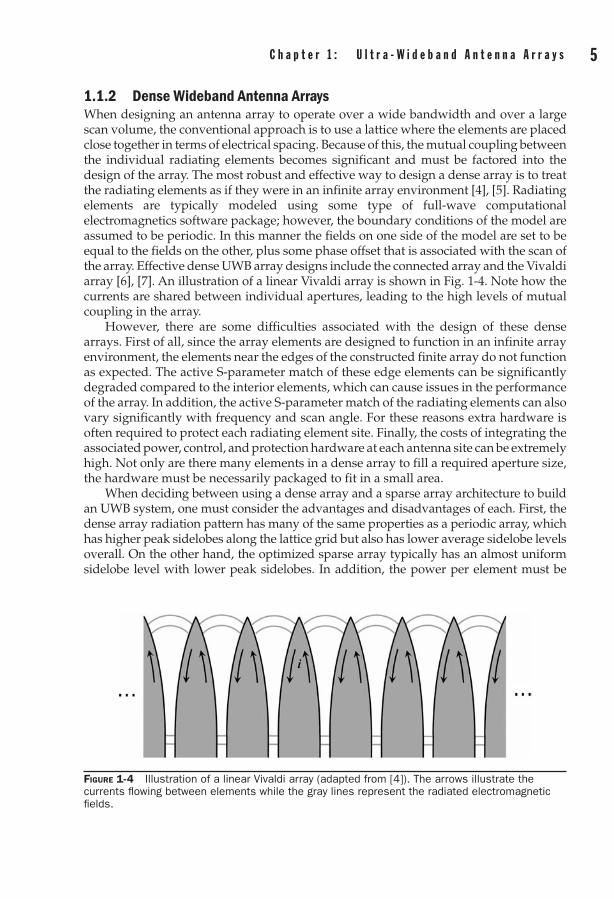
1.1.2 Dense Wideband Antenna ArraysWhen designing an antenna array to operate over a wide bandwidth and over a large scan volume, the conventional approach is to use a lattice where the elements are placed close together in terms of electrical spacing. Because of this, the mutual coupling between the individual radiating elements becomes significant and must be factored into the design of the array. The most robust and effective way to design a dense array is to treat the radiating elements as if they were in an infinite array environment [4], [5]. Radiating elements are typically modeled using some type of full-wave computational electromagnetics software package; however, the boundary conditions of the model are assumed to be periodic. In this manner the fields on one side of the model are set to be equal to the fields on the other, plus some phase offset that is associated with the scan of the array. Effective dense UWB array designs include the connected array and the Vivaldi array [6], [7]. An illustration of a linear Vivaldi array is shown in Fig. 1-4. Note how the currents are shared between individual apertures, leading to the high levels of mutual coupling in the array.
However, there are some difficulties associated with the design of these dense arrays. First of all, since the array elements are designed to function in an infinite array environment, the elements near the edges of the constructed finite array do not function as expected. The active S-parameter match of these edge elements can be significantly degraded compared to the interior elements, which can cause issues in the performance of the array. In addition, the active S-parameter match of the radiating elements can also vary significantly with frequency and scan angle. For these reasons extra hardware is often required to protect each radiating element site. Finally, the costs of integrating the associated power, control, and protection hardware at each antenna site can be extremely high. Not only are there many elements in a dense array to fill a required aperture size, the hardware must be necessarily packaged to fit in a small area.
When deciding between using a dense array and a sparse array architecture to build an UWB system, one must consider the advantages and disadvantages of each. First, the dense array radiation pattern has many of the same properties as a periodic array, which has higher peak sidelobes along the lattice grid but also has lower average sidelobe levels overall. On the other hand, the optimized sparse array typically has an almost uniform sidelobe level with lower peak sidelobes. In addition, the power per element must be
Figure 1-4 Illustration of a linear Vivaldi array (adapted from [4]). The arrows illustrate the currents flowing between elements while the gray lines represent the radiated electromagnetic fields.

6 F r o n t i e r s i n a n t e n n a s : N e x t G e n e r a t i o n D e s i g n & e n g i n e e r i n g C h a p t e r 1 : U l t r a - W i d e b a n d a n t e n n a a r r a y s 7
higher in a sparse array, because there are fewer elements. However, the hardware costs for a dense array can be significantly more expensive than the sparse array because there are more elements and it must accommodate the mutual coupling effects of the neighboring elements. The bandwidth achievable by these two types of arrays can be ultra-wide (>10:1) [4]; however, it is difficult to compare them since the challenges and solutions offered by each are very different. The bandwidth of a dense array is dependent on the system as a whole, because all of the elements are essentially connected; however, the bandwidth of a sparse array can theoretically be extremely large and is limited only by which antenna element is employed in the final design. This fact, along with the extra area provided per element, allows for the integration of different antenna technology and interleaving of antenna arrays [73]. Table 1-1 illustrates the trade-offs between these two array technologies. Depending on the application, one array technology may be more appropriate than the other.
1.1.3 Early Aperiodic Design MethodsSince the early 1960s, when it was first discovered that placing antenna elements in an aperiodic layout can yield radiation patterns devoid of grating lobes, many array design techniques have been proposed that attempt to provide array thinning with no grating lobes and low sidelobe levels [8]–[12]. Arrays with randomly located elements have become popular as a way to avoid grating lobes over wide bandwidths, but they are often plagued with high peak sidelobe levels [8], [17]–[20]. These arrays are usually uniformly excited when the main beam is steered to broadside since this is the easiest method for practical implementations.
Early designs using mathematically-determined element locations were presented in [21], although the small number of elements considered in these arrays significantly limited their performance. Modifications to basic array layouts such as the planar ring array yielded modest bandwidths in [22], where space-tapering of uniformly excited, isotropic elements was used to emulate a specific aperture amplitude distribution. Space-tapering, covered in detail in [23], was introduced as a method for enlarging an array aperture without requiring an unrealistically large number of antenna elements (which a periodic array would require), as well as reducing the sidelobe level of the arrays.
Table 1-1 Trade-Offs Between Dense and Sparse UWB Antenna Arrays
Property Dense Array Sparse Array
Variance of the Antenna Match High Low
Average Sidelobe Levels Low Moderate
Peak Sidelobe Levels Moderate Low
Hardware Density High Low
Power Per Element Low High
Aperture Size Needed Small Large
Number of Elements for an Aperture Many Few
Coupling Strong Weak
Achievable Bandwidth >10:1 >>10:1

6 F r o n t i e r s i n a n t e n n a s : N e x t G e n e r a t i o n D e s i g n & e n g i n e e r i n g C h a p t e r 1 : U l t r a - W i d e b a n d a n t e n n a a r r a y s 7
The tapering introduces aperiodicity into the array layout, which suppresses the grating lobes observed in Fig. 1-3. Increased array bandwidth was occasionally a design goal of space-tapering, but most often a byproduct of attempting to create large, thinned arrays with low sidelobe levels [24], [25].
More recently, new and potentially transformative approaches such as the fractal-random array began to appear in the literature. Unlike deterministic fractal arrays, fractal-random arrays are not restricted to the repetitive application of a single generator (see Section 1.2.1.1) and are therefore able to retain the beneficial aspects of both deterministic and random arrays. The random application of random generators leads to arrays with large bandwidths and moderate sidelobe levels [13]–[15]. Although the sidelobe levels associated with fractal-random arrays were too high for many practical applications, their introduction set the stage for the development of some very powerful UWB array design techniques, which will be covered in the following section. With the introduction of fractal and fractal-random arrays, the underlying concepts of array representation began to emerge. Array representation is the combination of a relatively small set of parameters with a mathematical construct (such as fractals) to define complex linear, planar, or volumetric array layouts. The following sections illustrate the usefulness of (and often prerequisite) array representation techniques for designing UWB antenna arrays.
This chapter will focus on providing an overview of new design methodologies for sparse UWB array architectures. The chapter will begin by discussing the foundations of multiband and UWB array design techniques. In addition, the mathematical foundations used to describe these complicated geometries and the optimization toolkits employed to synthesize sparse arrays are described. After that, the specific methodologies and techniques behind the construction of sparse arrays are discussed in detail. Finally, several linear and planar UWB sparse array design examples are presented, including experimental (measured) results for a sparse linear UWB array prototype.
1.2 Foundations of Multiband and UWB Array DesignBecause of the performance limitations of early aperiodic array designs, the most recent UWB antenna array design methodologies often employ some form of optimization in combination with an array representation technique to determine the best element positions for obtaining very large bandwidths and low sidelobe levels. Some of the first optimized aperiodic array designs used only a few elements due to limitations in the optimization strategy and simulation tools such as those reported in [26], where elements in a linear periodic array were perturbed by a genetic algorithm (GA). Since the variable position of each element is mapped to a corresponding GA parameter, optimization of a large array can quickly overwhelm the algorithm, therefore limiting the design size. These arrays typically possessed small bandwidths and, although the focus was mainly on reducing grating lobes and sidelobes during scanning (along with a controlled input impedance), beam steering is analogous to an increase in bandwidth.
There has been a great deal of investigation into ways of exploiting geometrical and mathematical concepts to design array layouts that contain inherent aperiodicity. As mentioned before, random arrays are inherently aperiodic, but leave little control to the array designer for obtaining better performance. The fractal-random arrays

8 F r o n t i e r s i n a n t e n n a s : N e x t G e n e r a t i o n D e s i g n & e n g i n e e r i n g C h a p t e r 1 : U l t r a - W i d e b a n d a n t e n n a a r r a y s 9
are an excellent starting point for UWB array design, since some type of user control can be implemented in the form of fractal generator selection and structure. Background on fractal theory will be provided here as it applies to the design of fractal-random, fractal multiband, and polyfractal antenna arrays. Other forms of aperiodic array representations are also discussed as alternatives for linear arrays or for the design of planar arrays. Lastly, a brief overview of the optimization strategies that are employed for the determination of UWB array layouts is given as it is a crucial part of all of the aforementioned design methods.
1.2.1 Fractal Theory and Its Applications to Antenna Array DesignFractal theory is a relatively new field of mathematics that has revolutionized the way scientists view the natural world. Derived from the Latin word meaning to break apart, the term fractal was originally coined by Mandelbrot [27] to describe a family of complex shapes that possess an inherent self-similarity or self-affinity in their geometrical structure. These intricate iterative geometrical oddities first troubled the minds of mathematicians around the turn of the twentieth century, where fractals were used to visualize the concept of the limit in calculus. What particularly confounded the mathematicians is that when they carried the limit to infinity properties of these objects such as arc length would also go to infinity, yet the object would remain bounded by a given area. However, it was only during the mid 1970s that a classification was assigned to these objects and the full significance of fractal theory began to come to light: Fractal objects appear over and over throughout nature and are the product of simple stochastic mechanisms at work in the natural world. Fractal patterns often represent the most efficient solutions to achieving a goal, whether it be draining water from a basin or delivering blood throughout the human body. These objects have also been used to describe the structures of ferns and trees, the erosion of mountains and coastlines, and the clustering of stars in a galaxy [28]. For these reasons, it is desirable to utilize the power of fractal geometry to describe the layout of antenna arrays. This section outlines several methods that are employed to construct fractal-based array geometries. In addition, this section also introduces a generalization of fractal geometry, called polyfractal geometry. Finally, a discussion is included about ways the self-similar properties of fractal and polyfractal arrays can be exploited to create rapid beamforming algorithms, which can be applied to improve the overall speed of fractal-based array optimizations.
1.2.1.1 Iterated Function SystemsIterated Function Systems (IFS) are powerful mathematical toolsets that are used to construct a broad spectrum of fractal geometries [28], [29]. These IFS are constructed from a finite set of contraction mappings, each based on an affine linear transformation performed in the Euclidean plane [29]. The most general representation of an affine linear transformation, wn consists of six real parameters (an , bn , cn , dn , en , fn) and is defined as
′′
=
=
xy
xy
ac
bd
xyn
n
n
n
nω +
efn
n (1-3)
or equivalently as
w x y a x b y e c x d y fn n n n n n n( , ) ( , ).= + + + + (1-4)

8 F r o n t i e r s i n a n t e n n a s : N e x t G e n e r a t i o n D e s i g n & e n g i n e e r i n g C h a p t e r 1 : U l t r a - W i d e b a n d a n t e n n a a r r a y s 9
The parameters of the IFS are often expressed using the compact notation
a bc d
ef
n n
n n
n
n
(1-5)
where coordinates x and y represent a point belonging to an initial object and coordinates x′ and y′ represent a point belonging to the transformed object. This general transformation can be used to scale, rotate, shear, reflect, and translate any arbitrary object. The parameters an , bn , cn, and dn control rotation and scaling while en and fn control linear translation. Consider a set of N affine linear transformations, w1 , w2 , . . . , wN. This set of transformations forms an IFS that can be used to construct a fractal of stage ℓ + 1 from a fractal of stage ℓ
F W F w Fnn
N
ℓ ℓ U+=
= =11
( ) ( )ℓ (1-6)
where W is known as the Hutchinson operator [28] and Fℓ is the fractal of stage ℓ. The
pattern produced by the Hutchinson operator is referred to as the generator of the fractal structure. If each transformation reduces the size of the previous object, then the Hutchinson operator can be applied an infinite number of times to generate the final fractal geometry, F∞. For example, if set F0 represents the initial geometry, then this iterative process would yield a sequence of Hutchinson operators that converge upon the final fractal geometry F∞.
F W F F W F F W F F W Fk k1 0 2 1 1= = = =+ ∞ ∞( ), ( ), , ( ), , ( )K K (1-7)
If the IFS is truncated at a finite number of stages L, then the object generated is said to be a prefractal image, which is often described as a fractal of stage L.
The IFS procedure for generating an inverted Sierpinski gasket is demonstrated in Fig. 1-5. In this case, the initial, stage-0 fractal, F0, is an inverted equilateral triangle. Three affine linear transformations, defined in Table 1-2, are applied to F0 and combined using equation (1-6) to create the stage-1 fractal, F1. These affine linear transformations are then applied and combined again to create the stage-2 fractal, F2. Higher-order versions of the inverted Sierpinski gasket are generated by simply repeating the iterative process until the desired resolution is achieved. This sequence of curves eventually converges to the actual inverted Sierpinski gasket fractal (illustrated in Fig. 1-6) as the number of iterations approaches infinity.
Table 1-2 IFS Code for Generating an Inverted Sierpinski Gasket
w a b c d e f
1 1/2 0 0 1/2 0 3 4/
2 1/2 0 0 1/2 1/2 3 4/
3 1/2 0 0 1/2 1/4 0

10 F r o n t i e r s i n a n t e n n a s : N e x t G e n e r a t i o n D e s i g n & e n g i n e e r i n g C h a p t e r 1 : U l t r a - W i d e b a n d a n t e n n a a r r a y s 11
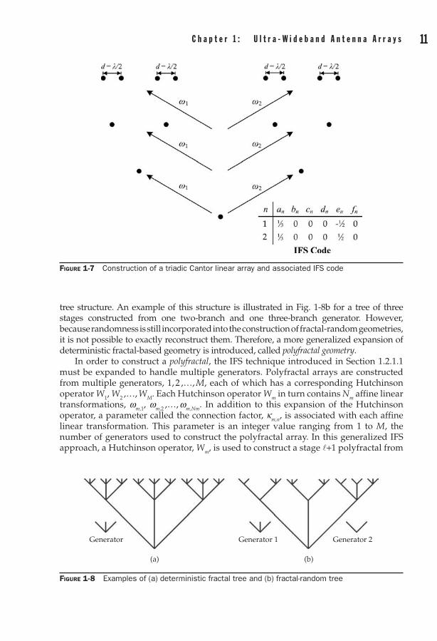
Finally, an IFS process is illustrated in Fig. 1-7 for the construction of a stage four triadic Cantor linear array. The IFS operates on the individual antenna elements, which in this example are represented by the points of the Cantor set. The final array is scaled such that the minimum spacing between points is equal to l/2.
1.2.1.2 Polyfractal Iterated Function SystemsThe IFS approach is the most common method used to construct deterministic fractal geometries; however, deterministic fractals may not resemble natural objects very closely because of their perfect symmetry and order. On the other hand, random fractals more closely resemble natural objects because their geometries are often created using purely stochastic means. However, these objects are difficult to work with, especially in the context of optimization, because their structures cannot be recreated with exact precision. In an effort to bridge the gap between deterministic and random fractals, a specialized type of fractal geometry, called a fractal-random tree, was developed. This new construct combines together properties of both deterministic and random fractal geometries [14], [15]. An example of a deterministic fractal tree is shown in Fig. 1-8a. A ternary (three-branch) generator is used for the first three stages of growth. Alternatively, a fractal-random tree is constructed from multiple deterministic generators selected in random order to form the
Figure 1-6 Final inverted Sierpinski gasket geometry
Figure 1-5 Generation of the first two stages of an inverted Sierpinski gasket
10 F r o n t i e r s i n a n t e n n a s : N e x t G e n e r a t i o n D e s i g n & e n g i n e e r i n g C h a p t e r 1 : U l t r a - W i d e b a n d a n t e n n a a r r a y s 11
tree structure. An example of this structure is illustrated in Fig. 1-8b for a tree of three stages constructed from one two-branch and one three-branch generator. However, because randomness is still incorporated into the construction of fractal-random geometries, it is not possible to exactly reconstruct them. Therefore, a more generalized expansion of deterministic fractal-based geometry is introduced, called polyfractal geometry.
In order to construct a polyfractal, the IFS technique introduced in Section 1.2.1.1 must be expanded to handle multiple generators. Polyfractal arrays are constructed from multiple generators, 1, 2 ,…, M, each of which has a corresponding Hutchinson operator W1, W2 ,…, WM. Each Hutchinson operator Wm in turn contains Nm affine linear transformations, wm,1, wm,2 ,…, wm,Nm. In addition to this expansion of the Hutchinson operator, a parameter called the connection factor, km,n, is associated with each affine linear transformation. This parameter is an integer value ranging from 1 to M, the number of generators used to construct the polyfractal array. In this generalized IFS approach, a Hutchinson operator, Wm, is used to construct a stage ℓ+1 polyfractal from
Figure 1-7 Construction of a triadic Cantor linear array and associated IFS code
Figure 1-8 Examples of (a) deterministic fractal tree and (b) fractal-random tree
(a) (b)
Generator Generator 1 Generator 2

12 F r o n t i e r s i n a n t e n n a s : N e x t G e n e r a t i o n D e s i g n & e n g i n e e r i n g C h a p t e r 1 : U l t r a - W i d e b a n d a n t e n n a a r r a y s 13
the set of possible stage ℓ polyfractals, Fℓ. Each affine linear transformation, wm,n, can
only be performed on stage ℓ polyfractals, where the generator applied at stage ℓ matches the connection factor, km,n. Because the connection factors dictate how the affine linear transformations are applied, only one unique polyfractal geometry can be associated with each Hutchinson operator. Therefore, the set of stage ℓ polyfractals, F
ℓ,
can be expressed by the following notation:
F F F F Mℓ ℓ ℓ ℓK= , , , , , ,1 2 (1-8)
where the first subscript defines the level of the polyfractal and the second subscript defines the generator employed at that level. Therefore, a polyfractal of stage ℓ+1 constructed by generator m can be represented by
F W F F F w Fm m M m nn
Nm
ℓ ℓ ℓ ℓK U+=
= =1 1 21
, , , , , ,( , , , ) ℓ κκm n,( ) (1-9)
As another example to demonstrate how the modified IFS procedure operates, a polyfractal example based on the inverted Sierpinski gasket is discussed. In this example, two generators are used to construct two inter-related polyfractal geometries. One of these generators consists of three transformations and is based on the inverted Sierpinski gasket generator. The second consists of four transformations and creates a complete triangle pattern. In addition, each of these affine linear transformations has an associated connection factor that specifies to which of the interrelated polyfractal geometries the transformation is applied. The parameters for each of these transformations and the associated connection factors are listed in Table 1-3. In addition, a visual representation of these transformations and their associated connection factors are illustrated in Fig. 1-9. Similar to the process used to construct a deterministic fractal, these generators are applied to an initial geometry F0 and combined using (1-9) to create the set of stage-1 polyfractal geometries, F1,1 and F1,2. Geometry F1,1 is created by generator 1 and geometry F1,2 is created by generator 2. Next, the generators are applied to the set of stage-1 polyfractals, where the transformations associated with a connection factor of 1 operate on F1,1 and transformations associated with a connection factor of 2 operate on F1,2.
w a b c d e f : k
Generator 1
1 1/2 0 0 1/2 0 3 4/ : 1
2 1/2 0 0 1/2 1/2 3 4/ : 1
3 1/2 0 0 1/2 1/4 0 : 2
Generator 2
1 1/2 0 0 1/2 0 3 4/ : 2
2 1/2 0 0 1/2 1/2 3 4/ : 1
3 1/2 0 0 1/2 1/4 0 : 2
4 1/2 0 0 –1/2 1/4 3 2/ : 1
Table 1-3 IFS Code and Associated Connection Factors for Sierpinski-Based Polyfractal Geometries
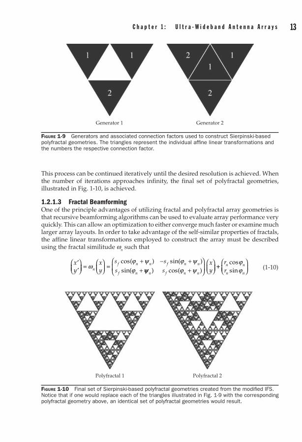
12 F r o n t i e r s i n a n t e n n a s : N e x t G e n e r a t i o n D e s i g n & e n g i n e e r i n g C h a p t e r 1 : U l t r a - W i d e b a n d a n t e n n a a r r a y s 13
This process can be continued iteratively until the desired resolution is achieved. When the number of iterations approaches infinity, the final set of polyfractal geometries, illustrated in Fig. 1-10, is achieved.
1.2.1.3 Fractal BeamformingOne of the principle advantages of utilizing fractal and polyfractal array geometries is that recursive beamforming algorithms can be used to evaluate array performance very quickly. This can allow an optimization to either converge much faster or examine much larger array layouts. In order to take advantage of the self-similar properties of fractals, the affine linear transformations employed to construct the array must be described using the fractal similitude wn such that
′′
=
=++
xy
xy
s
snf n n
f n
ωϕ ψϕ
cos( )sin( ψψ
ϕ ψϕ ψn
f n n
f n n
s
sxy)
sin( )cos( )
- ++
++
rrn n
n n
cossin
ϕϕ (1-10)
Generator 1 Generator 2
Figure 1-9 Generators and associated connection factors used to construct Sierpinski-based polyfractal geometries. The triangles represent the individual affine linear transformations and the numbers the respective connection factor.
Figure 1-10 Final set of Sierpinski-based polyfractal geometries created from the modified IFS. Notice that if one would replace each of the triangles illustrated in Fig. 1-9 with the corresponding polyfractal geometry above, an identical set of polyfractal geometries would result.
Polyfractal 1 Polyfractal 2

14 F r o n t i e r s i n a n t e n n a s : N e x t G e n e r a t i o n D e s i g n & e n g i n e e r i n g C h a p t e r 1 : U l t r a - W i d e b a n d a n t e n n a a r r a y s 15
This similitude is constructed using three local parameters, rn, jn, yn; and one scale parameter sf (in polyfractal geometries, the subscript n is replaced with the subscript n, m). In this way, each fractal and polyfractal subarray is identical. Therefore, it follows that the radiation patterns of each of these subarrays are identical.
Many fractal array recursive beamforming algorithms are based on the pattern multiplication approach. The radiation pattern of a stage ℓ fractal array is equal to the product of the radiation pattern of a stage ℓ-1 fractal subarray and the array factor of the appropriately scaled fractal generator. In other words, the stage ℓ fractal array can be thought of as an array of stage ℓ-1 fractal subarrays. In order to perform pattern multiplication, not only must all subarray radiation patterns be identical, they must also be oriented in the same direction. Therefore, the sum of jn and yn is required to be equal to a multiple of 2p, making the axes of symmetry of the subarrays parallel. The equation for a recursive beamforming algorithm based on pattern multiplication can be written as
FR FR j k s s rL Lg f
Lnℓ ℓ
ℓ( , ) ( , ) exp ( ) sinθ ϕ θ ϕ θ= ( )--
1 ccos( )ϕ ϕ-
=
∑ nn
N
1 (1-11)
where k is the free-space wavenumber and sg is a global scale parameter used to ensure minimum spacing between elements. Assuming isotropic sources as the initial subarray radiation pattern, the final stage L fractal array factor can be written in a similar manner as has been done in [30]:
AF j k S rLL
n nn
N
( , ) exp sin cos( )θ ϕ δ θ ϕ ϕ= - -
=
ℓ 1
1∑∑∏
=ℓ 1
L (1-12)
where d = 1/sf and S = sg (sf)L-1. Typically, the values of rn are scaled such that S can be set
equal to one.The unique scaling procedure and connection factor based construction allow the
rapid recursive beamforming algorithms associated with fractal arrays to be generalized to handle polyfractal arrays. The fractal array recursive beamforming operation discussed above requires all subarrays to have the same radiation pattern and be oriented in the same direction. In that way, pattern multiplication can be employed. In the more general polyfractal array, there are multiple types of subarrays that do not necessarily point in the same direction. Therefore these subarray patterns cannot be factored out of the summation and the resulting expression for the stage ℓ, generator m subarray pattern is given by
FR FRmL L
m n m nn
m nℓ ℓ, , , ,( , ) ( , ),
θ ϕ θ ϕ ϕ ψκ= - -( )-=
11
NN
g fL
m n m n
m
j k s s r
∑
× ( ) -
-exp ( ) sin cos( ), ,ℓ θ ϕ ϕ
(1-13)
This subarray radiation pattern is based on the set of stage ℓ-1 fractal subarray patterns. The final radiation pattern can be determined by using isotropic sources for the initial subarray radiation patterns and recursively applying the expression until the stage L radiation pattern is obtained. Figure 1-11 illustrates this process for an example based on a two-generator (three-branch and four-branch) polyfractal array. One of the main

14 F r o n t i e r s i n a n t e n n a s : N e x t G e n e r a t i o n D e s i g n & e n g i n e e r i n g C h a p t e r 1 : U l t r a - W i d e b a n d a n t e n n a a r r a y s 15
advantages of the recursive beamforming approaches associated with fractal and polyfractal arrays is that they can be exploited to considerably speed up the convergence of the GA. This allows the possibility of optimizing much larger arrays than those that have previously been achievable using other approaches.
1.2.1.4 Multiband Fractal ArraysThe self-similar properties of fractals have been utilized in antenna array design to develop multiband radiation pattern synthesis techniques [13], [15], [31]–[37]. An approach was first introduced in [31] for synthesizing Weierstrass fractal radiation patterns based on a family of nonuniformly spaced self-scalable linear arrays of discrete elements, which are called Weierstrass arrays. In addition, a Fourier-Weierstrass fractal radiation pattern synthesis technique was presented in [31] for continuous line sources. The radiation properties of concentric circular arrays that incorporate Weierstrass and Cantor fractals into their design have been considered in [32] and [13], respectively. Properties of Weierstrass fractals were first employed in [33] to develop a multiband array synthesis technique. Application of fractal concepts to the design of multiband Koch arrays as well as low sidelobe Cantor arrays are discussed in [34]. In [36], a novel fractal-inspired design methodology was introduced for reconfigurable multiband linear and planar arrays. A special class of atomic functions was later studied in [37] and shown to provide additional design flexibility for multiband (reconfigurable) fractal arrays. A more comprehensive overview of the theory and design techniques for fractal arrays can be found in [15], [35].
In this section, we focus on the radiation pattern synthesis technique for designing reconfigurable multiband arrays that was first considered in [36]. This technique is based on a generalization of the conventional Fourier series synthesis approach and
Figure 1-11 Illustration of the rapid recursive beamforming algorithm for a two-generator polyfractal array (after J. S. Petko and D. H. Werner, IEEE 2005, Ref. [48])

16 F r o n t i e r s i n a n t e n n a s : N e x t G e n e r a t i o n D e s i g n & e n g i n e e r i n g C h a p t e r 1 : U l t r a - W i d e b a n d a n t e n n a a r r a y s 17
achieves the desired multiband performance by utilizing radiation patterns that exhibit self-similar fractal properties. Suppose we consider a series of P self-scalable linear arrays, each with a total of 2N + 1 elements oriented along the z-axis and centered about the origin, such that the total number of elements in the composite array would be P(2N + 1). Furthermore, if we assume that the current amplitude distribution on each of the P subarrays is symmetric (i.e., I-n = In), then the array factor may be expressed in the following form [36]:
AF w C I I W wNP
P n nP
n
N
( ) ( )= +=
∑01
2 (1-14)
where
W ws
nk ds w wnP
pp
p
P
( ) cos ( )=
-
--
=
11
10
1 γ∑∑ (1-15)
Cs
s
P
P
=-
-
11
11
γ
γ
(1-16)
Id
f w nd
w dwnd=
2 202
λπ
λ
λ
( )cos∫∫ (1-17)
The remaining parameters are defined as w = cosq, where q is measured from the z-axis, w0 = cosq0, where q0 represents the desired position angle of the main beam, s is the scaling or similarity factor, g is an additional current amplitude scaling parameter, and f(w) is a desired generating or window function with the property that f(–w) = f(w). Note that for the special case when P = 1, expression (1-14) reduces to
AF w I I nkd w wN nn
N1
0 01
2( ) cos[ ( )]= + -=
∑ (1-18)
which represents the array factor for a conventional linear array comprised of 2N + 1 elements spaced a uniform distance d apart with a nonuniform symmetrical (i.e. I–n = In) current amplitude excitation. If N → ∞ then (1-18) represents a Fourier series on the interval - < <λ λ
2 2d dw such that
Id
AF w nd
w dwn =
2 210λ
πλ
λ
( )cos22d∫ (1-19)
where
lim ( ) ( ) cos[ ( )]N N n
n
AF w AF w I I nk d w w→∞ =
= = + -1 10 02
11
∞
∑ (1-20)
The array factor expression given in (1-14), which results from a superposition of self-scalable linear arrays, can be related to the radiation properties of Fourier-Weierstrass

16 F r o n t i e r s i n a n t e n n a s : N e x t G e n e r a t i o n D e s i g n & e n g i n e e r i n g C h a p t e r 1 : U l t r a - W i d e b a n d a n t e n n a a r r a y s 17
arrays provided that 1 1s < <γ [15], [31], [35]. Under these conditions, it can be shown that Wn
P(w) represent bandlimited Weierstrass functions. The fractal dimension D associated with these Weierstrass functions as P → ∞ is given by
D = -1ln( )ln(s)
γ (1-21)
If we consider an array with a doubly infinite number of stages, then it can be shown that [36]
AF (a w) = ab AF (w) (1-22)
where
AF w AF wP
P( ) lim ( )=→∞
(1-23)
AF ws
s s
PP
( )( )
=-
-
- +
11
1 11
γ
γ γ
PP
n pnp
npI nk ds w
-
=
∞∑ ε cos 11
0==-
=
∞
∑∑+
P
P
nnI I0 1
(1-24)
εnnn
= =>
12
00
,,
(1-25)
k11
2= πλ
(1-26)
d = al1 (a is a dimensionless parameter) (1-27)
αλλ
= = =
> =-
1
1
11
1 1 2m
mmf
f sf s mor and , ,L (1-28)
βγ
γ=
>-
1 11m
sand (1-29)
and where f1 represents the base-band design frequency of the array. Based on (1-22) it follows that this array will exhibit multiband behavior when operated at the discrete set of frequencies defined by the relationship given in (1-28). We note that this multiband property holds for infinite arrays, but rapidly degrades once the arrays are truncated. In order to compensate for these truncation effects, a novel reconfigurable band-switching technique was proposed in [36].
The multiband radiation pattern synthesis technique developed thus far for linear arrays can be readily extended to include planar array configurations. Suppose that we have a sequence of self-scalable planar arrays that lie in the xy-plane and are centered about the origin, then the composite far-field radiation pattern may be expressed in the form
AF u v I mk dsNP
mn
N
m
N
p
P
n pmnp( , ) cos=
===
-∑∑∑ ε111
1 (( )
cos ( )
u u
nk ds v vp
-
× - -
0
10
(1-30)
18 F r o n t i e r s i n a n t e n n a s : N e x t G e n e r a t i o n D e s i g n & e n g i n e e r i n g C h a p t e r 1 : U l t r a - W i d e b a n d a n t e n n a a r r a y s 19
where
Is
Is
I Ipmn
p
mn
p
m n=
=
- -1 1
1 1
γ γ (1-31)
Ikd
f w qk dw dw q m nqkd=
=∫π
π
( )cos [ ] for or0
(1-32)
u = sinq cosf (1-33)
v = sinq sinf (1-34)
u0 = sinq0 cosf0 (1-35)
v0 = sinq0 sinf0 (1-36)
This synthesis procedure yields planar arrays with nonperiodic element layouts that produce two-dimensional (2D) self-similar (fractal) radiation patterns, which are based on scaled and translated versions of a specified generating function f(w). Several examples of useful generating or window functions f(w) are provided in Table 1-4, along with the corresponding expressions for the Fourier cosine series coefficients Iq evaluated using (1-32) [36], [37]. These window functions can be employed to synthesize massively thinned multiband arrays with dramatically reduced element counts and, as a consequence, much smaller aperture sizes.
1.2.2 Aperiodic Tiling TheoryWe start this section by giving some basic definitions regarding tiles and tilings. In general, a tiling is a partition of space into a countable number of tiles in such a way that every point in space belongs to at least one tile, and in the case that a point belongs to more than one tile, it must be on the boundary of those tiles. Put in mathematical notation, a tiling Ξ of the space Ed is a countable set of tiles [38]
Ξ = T1,T2, . . . (1-37)
such that the union of all the tiles is Ed (d denotes the dimension of the space) and the intersection of the interiors of any two tiles is the empty set. The above definition does not put any restriction on the shapes of the tiles, or the number of possible shapes. However, since we are studying tiles for their applications to antenna arrays, we limit our attention to those tilings whose tiles are copies of a finite set of shapes. The elements of this finite set of shapes are known as prototiles. As a very basic example consider the tiling of the 2D plane (E2) by identical squares whose side is unity. In such a case the tiling is defined by only one prototile, namely a unit square. The 2D plane can also be tiled by a chessboard pattern. In this case the tiling is defined by two prototiles: one black square and one white square. Tilings can be either periodic or aperiodic. In order to establish periodicity in Ed, we must be able to find d basis vectors u1, u2 ,. . ., ud such that
T(p) = T (p + m1 u1 + m2 u2 + · · · +md ud) m1, m2 , . . . , md = 0, ±1, ±2, . . . (1-38)
In the preceding equation, p denotes the location of a point in Ed and T(p) denotes the prototiles in that location. For our first example (tiling of the plane with unit squares) assuming that our plane is the xy-plane, by inspection we can see that for u1 = x and

18 F r o n t i e r s i n a n t e n n a s : N e x t G e n e r a t i o n D e s i g n & e n g i n e e r i n g C h a p t e r 1 : U l t r a - W i d e b a n d a n t e n n a a r r a y s 19
Table 1-4 Some Useful Window Functions and the Coefficients for Their Associated Fourier Cosine Series
Window Function f (w) Fourier Series Coefficients Iq
Blackman Window
a aw
aw
0 1
2
22
42
-+
∆
∆
+
+∆
cos
cos
π
π
∆
-
+∆
∆
0
62
3
,
cosawπ
,,
otherwise
-∆
≤ ≤∆
2 2w
where
a0 = 0.42, a
1 = 0.5, and a
2 = 0.08
akd qkd
akd
0
1
2 2
2 2
π
π
+
∆∆
∆
sinc
-
+
sincqkd
akd
∆
∆2
2 21
π
π +
+
sin
si
cqkd
akd
∆
∆2
2 22
π
πnn
sin
c
c
qkd
akd q
∆
∆2
2
2 22
-
+
π
πkkd∆2
2+
π
Blackman-Harris Window
a aw
aw
0 1 2
22
42-
+∆
∆
+
+∆
cos cos
π π
∆
-
∆≤ ≤
∆
-+
∆
∆
2 2
62
3
w
aw
cosπ
otherwise
0
where
a a a a0 0 35875 0 48829 0 14128= = = =. , . , . , and1 2 3 00 01168.
akd qkd
akd
0
1
2 2
2 2
π
π
+
∆∆
∆
sinc
-
+
sincqkd
akd
∆
∆2
2 21
π
π +
+
sin
si
cqkd
akd
∆
∆2
2 22
π
πnn
sin
c
c
qkd
akd q
∆
∆2
2
2 22
-
+
π
πkkd
akd qkd
∆
∆ ∆2
2
2 23
+
+
π
πsinc
223
2 2 233
-
+
-
π
πa
kd qkd∆ ∆sinc ππ
Kaiser-Bessel Window
Iw
Iw
0
2
0
12
2
2 2
0
πα
πα
-∆
-∆
≤ ≤∆
( )
otherwwise
where a ∈
≅
-
kd
I
qkd
2
2
0
22
π πα
πα∆ ∆
( )
sin ( )h
-
( )π α 2
22qkd
∆
Kravchenko Window No. 1
fupn (w ) where n = 0, 1, 2, . . .
sin sinc cn j
j
qkd qkd∆ ∆2
1
2 22
1
-
=
∞
∏
Kravchenko Window No. 2
Ξn (w ) where n = 1, 2, 3, . . .
sin ( )c n j
j
qkdn
∆2
11
+
-
=
∞
∏
Kravchenko Window No. 3
ha (w ) where a ∈
sinqkd
a
a
j
jj
∆221
-
-=
∞
∏

20 F r o n t i e r s i n a n t e n n a s : N e x t G e n e r a t i o n D e s i g n & e n g i n e e r i n g C h a p t e r 1 : U l t r a - W i d e b a n d a n t e n n a a r r a y s 21
u2 = y, we can establish the periodicity of the tiling. Similarly, for the second example the periodicity can be established for u1′ = 2x and u2′ = 2y. It is worth mentioning that the set of basis vectors will not be unique. A periodic tiling is said to have translational symmetry. An example of a periodic tiling with two prototiles and its basis vectors is shown in Fig. 1-12. As mentioned earlier, the set of basis vectors is not unique. For the tiling in Fig. 1-12, two sets of basis vectors are shown.
In general any quadrilateral can form a periodic tiling of the plane. This is true for convex as well as concave quadrilaterals. Tilings can also be generated in an iterative process from fractals. These tilings are referred to as fractiles. A well-known example is the fudgeflake fractile [27]. Individual tilings are generated in an iterative process starting with a regular hexagon. The first six steps of the iteration process are shown in Fig. 1-13. At any iteration level, the resulting fractile can be used to periodically tile the plane. An example of tiling the plane with the sixth iteration of the fudgeflake fractile is shown in Fig. 1-14 [39]. Antenna array design approaches that employ fractals have been considered in [40]–[45]. Tilings can also be applied to curved surfaces. Figure 1-15 shows three different aperiodic tilings of a sphere using various sets of prototiles.
For an aperiodic tiling, the basis vectors u1, u2 ,..., ud that will satisfy the above periodicity condition do not exist. Figure 1-16 shows the pattern of an aperiodic tiling known as the Amman tiling, discovered by Robert Amman in 1977 [39]. Over the past 50 years, several sets of aperiodic tilings have been discovered. Probably the best known aperiodic tiling is the Penrose tiling discovered by Sir Roger Penrose in 1974 [46], [47] (Fig. 1-17). The tiling is built from only two prototiles. Once the prototiles are known, there are several ways to generate the tiling. Perhaps the most intuitive way is placing tiles next to each other according to specific matching rules, which are meant to preserve the aperiodicity of the tiling. The shortfall of this method is the fact that
Figure 1-12 An example of a periodic tiling generated by two prototiles A and B. Two sets of basis vectors are displayed.
Figure 1-13 First six iterations of the fudgeflake fractile

20 F r o n t i e r s i n a n t e n n a s : N e x t G e n e r a t i o n D e s i g n & e n g i n e e r i n g C h a p t e r 1 : U l t r a - W i d e b a n d a n t e n n a a r r a y s 21
the tiling might be generated to a point at which no additional tiles can be added via matching rules.
A more systematic approach, which lends itself better to programming, is the use of an iterative inflation process [39], [48], [49]. This process is also known as stone inflation. Stone inflation specifies how each tile is first expanded by a given factor and then subdivided into smaller tiles. Figure 1-18 shows the two prototiles of the Penrose tiling. Figure 1-19 shows an illustration of the iterative inflation process. It is interesting to note that the number of tiles grows according to the Fibonacci sequence (1 → 2 → 3 → 5 → 8 → …).
Penrose tilings are not the only known aperiodic tilings of the plane. Some of the more well-known aperiodic tilings include chair, pinwheel, sphinx, and Danzer
Figure 1-14 Tiling of the plane with the sixth iteration of the fudgeflake fractile
Figure 1-15 Several examples showing aperiodic tilings of a curved surface with increasing complexity
(a) (b) (c)

22 F r o n t i e r s i n a n t e n n a s : N e x t G e n e r a t i o n D e s i g n & e n g i n e e r i n g C h a p t e r 1 : U l t r a - W i d e b a n d a n t e n n a a r r a y s 23
tilings [38], [39]. Danzer tilings in particular are of interest for antenna array applications. The Danzer tiling is comprised of three prototiles. Similar to a Penrose tiling, starting with the prototiles, the tiling can be generated by either placing the prototiles next to each other according to matching rules or by stone inflation. The prototiles of the Danzer aperiodic set are shown in Fig. 1-20. Figure 1-21 shows the iterative process applied to the third Danzer prototile in Fig. 1-20.
Figure 1-22 shows another type of aperiodic tiling known as the pinwheel tiling. The pinwheel tiling was proposed by John Conway and Charles Radin [50]. One interesting feature of this tiling is that it is comprised of only one prototile. Similar to the Penrose and the Danzer tiling, the pinwheel tiling can be generated using the substitution and inflation rules as demonstrated in Fig. 1-22.
Figure 1-17 Penrose aperiodic tiling
Figure 1-16 Amman aperiodic tiling

22 F r o n t i e r s i n a n t e n n a s : N e x t G e n e r a t i o n D e s i g n & e n g i n e e r i n g C h a p t e r 1 : U l t r a - W i d e b a n d a n t e n n a a r r a y s 23
Figure 1-18 Prototiles of the Penrose tiling θ π τ/= =( )+5 1 52and (From T. G. Spence, and D.H.
Werner, ©IEEE 2008, [59])
Figure 1-19 Iterative stone inflation of Penrose prototiles
Figure 1-21 Inflation and substitution applied to Danzer prototile type III
Figure 1-20 Prototiles of the Danzer tiling θ π=( )7 (From T. G. Spence, and D.H. Werner, ©IEEE 2008, [59])

24 F r o n t i e r s i n a n t e n n a s : N e x t G e n e r a t i o n D e s i g n & e n g i n e e r i n g C h a p t e r 1 : U l t r a - W i d e b a n d a n t e n n a a r r a y s 25
The concept of aperiodic tilings can be further extended into three dimensions in order to generate volumetric aperiodic tilings. In 1989, Danzer discovered a set of four prototiles that can aperiodically tile the Euclidean three-dimensional (3D) space [51]. This tiling is composed of four prototiles in the shape of tetrahedrons and their mirror images. The four Danzer prototiles (A, B, C, K) are shown in Fig. 1-23. The values for the
edges are given in Table 1-5, where, τ / , / , / .= +( ) = +
=1 5 2 10 2 5 4 3 2a band
Once the prototiles are known, the tiling can be generated using the inflate-and-subdivide approach. Danzer derived the subdivision rules for this tiling [52]. The same rules are expressed in [53], but in a more precise manner using linear transformations and group theory. The subdivision rules act upon an initial tile and divide the tile into a number of different tiles all of which are in a scale of t –1 to one of the prototiles in Table 1-5. Thus after each subdivision, the tiling has to be scaled by t. Figure 1-24 shows two iterations of the subdivision rules, starting with prototile A.
1.2.3 Optimization TechniquesOne of the key aspects of the more recent high-performance UWB antenna array design methodologies is the incorporation of a robust global optimization strategy to improve
Figure 1-22 Pinwheel prototile and two iterations of substitution rules applied to it
Figure 1-23 The prototiles of a three-dimensional Danzer tiling (From F. Namin and D. H. Werner, IEEE 2010 [54])
A B C K
Edge
Tetrahedron 1-2 2-3 3-1 2-4 1-4 3-4
A a tb ta a 1 b
B a ta tb b t –1a 1
C t –1a tb t b a a
K a b t –1a t/2 1/2 t –1/2
Table 1-5 Lengths of the Edges of the three-dimensional Danzer Prototiles

24 F r o n t i e r s i n a n t e n n a s : N e x t G e n e r a t i o n D e s i g n & e n g i n e e r i n g C h a p t e r 1 : U l t r a - W i d e b a n d a n t e n n a a r r a y s 25
the performance of the final array designs [55]–[59]. The goal of the optimization strategy is to find the best set of design input parameters that define an array, which satisfies one or more UWB conditions. The UWB array design procedure, outlined in Fig. 1-25 is usually an iterative method based on the genetic algorithm (GA) [60]–[63], particle swarm (PS) [64]–[67], or some other global optimization technique.
The aforementioned algorithms operate by creating a group of parameter sets called a population, where each set is referred to as a population member. Each population member, by way of the array representation technique, defines a specific solution or aperiodic array design. At every algorithm iteration (also called a generation), the population is evaluated such that each population member has an accompanying fitness value or fitness vector in the case of multiobjective optimization. Subsequently, the algorithm uses knowledge of the population parameters and fitness (and possibly knowledge of past iterations) to form a new population. This process repeats until a suitable solution (acceptable UWB array design) is found, the algorithm converges (little fitness improvement is made in many iterations), or time is expired. A simplified schematic of the genetic algorithm optimization process is given in Fig. 1-26
The most significant difference between single-objective and multiobjective optimization strategies is the sorting and selection method. Single-objective is fairly straightforward; the best members which are ranked according to fitness prevail. This can be done with a tournament selection method, for example, where random population pairs are formed and the best member of each pair is passed on for crossover and mutation. With multiobjective fitness vectors, the selection process involves finding the set of nondominated solutions in the Pareto frontier [68]–[72], that is, a solution where no
Figure 1-24 Two iterations of the subdivision rules applied to prototile A (From F. Namin and D. H. Werner, IEEE 2010, [54])
Figure 1-25 Typical optimization strategy for designing an UWB array

26 F r o n t i e r s i n a n t e n n a s : N e x t G e n e r a t i o n D e s i g n & e n g i n e e r i n g C h a p t e r 1 : U l t r a - W i d e b a n d a n t e n n a a r r a y s 27
other solution has better fitness for all of the objectives. An example Pareto frontier with the dominated and nondominated solutions highlighted is given in Fig. 1-27. At the end of an optimization, the user selects one of the nondominated solutions as the final design, where a trade-off must be made between two or more goals.
For almost all of the algorithms, there are several evolutionary constants that must be specified, which determine their behavior. For example, the mutation rate of the genetic algorithm determines how many new and different population members are formed at each generation. Too large a mutation rate and the algorithm has trouble converging to good solutions, while at too small a rate the algorithm can converge quickly on unacceptable solutions. Careful selection of these constants must be heeded to obtain good algorithm performance. In addition to these evolutionary constants, other values such as the population size must be determined before beginning an optimization.
Figure 1-26 Simplified functional diagram of a single-objective genetic algorithm.
Figure 1-27 Example Pareto frontier for a two-objective optimization

26 F r o n t i e r s i n a n t e n n a s : N e x t G e n e r a t i o n D e s i g n & e n g i n e e r i n g C h a p t e r 1 : U l t r a - W i d e b a n d a n t e n n a a r r a y s 27
Generally, larger populations are used for more difficult problems. Because of the use of populations, most algorithms are well suited to parallelization, where multiple population members can be simultaneously evaluated on multiple computer processors. For very difficult design problems, i.e., arrays with thousands of elements, the use of parallel evaluation is usually recommended to obtain an acceptable solution in a reasonable amount of time. Once configured correctly, these optimization tools provide a powerful mechanism for obtaining UWB array designs.
1.3 Modern UWB Array Design TechniquesIn this section, several state-of-the-art UWB array design methodologies are introduced and specific application examples are provided for each technique. In addition to simply obtaining the best sidelobe level at a certain bandwidth, some designs require that more than one goal be achieved. For instance, with the multiobjective polyfractal design, multiple bandwidth goals can be targeted, giving the user a trade-off curve (Pareto front) from which to select an appropriate design after the optimization has been completed. With the raised-power series (RPS) design technique, the optimization is restricted to a specific number of elements, rather than specifying a range of elements or implementing this decision into the fitness function as is done in the case of polyfractal arrays. The polyfractal, RPS, and aperiodic tiling methods will be explained here, giving insight into which methods are best for various applications.
1.3.1 Polyfractal ArraysPolyfractal arrays were developed from a class of quasi-random arrays called fractal-random arrays [14], [55]–[57]. These structures, briefly introduced in Section 1.2.1.2, are used to generate array geometries that lie somewhere between completely ordered (i.e., periodic) and completely disordered (i.e., random). The primary advantage of this approach is that it yields sparse arrays that possess relatively low sidelobe levels, which are typically associated with periodic arrays, but over a range of bandwidths that are comparable to random arrays. Hence, fractal-random arrays bridge the gap between periodic and random arrays both structurally and functionally.
However, there is a significant shortcoming in fractal-random array theory that prevents it from being employed in conjunction with any kind of optimization technique. There is no reliable way to accurately recreate fractal-random geometries from a set of constructing parameters. Therefore, an effort was recently undertaken to identify a representative subset of fractal-random arrays that can be recreated deterministically in a repeatable manner. These arrays, called polyfractal arrays, perform similarly to fractal-random arrays yet their geometries can be described with fewer parameters and their specific recursive properties can be exploited in rapid beamforming algorithms. General construction techniques for polyfractals are discussed in Section 1.2.1.2, while specification of polyfractal arrays and associated rapid beamforming techniques are discussed in Section 1.2.1.3. It is the combination of the relatively small set of design parameters and available rapid beamforming algorithms that makes polyfractal arrays ideal candidates for optimization. These properties significantly speed up optimization convergence and as a result allow the study of much larger array sizes.
While polyfractal arrays are well suited for optimization, they offer even more advantages when specialized operators are tailored to handle their unique data structures. One of the most powerful operators available to polyfractal arrays stimulates
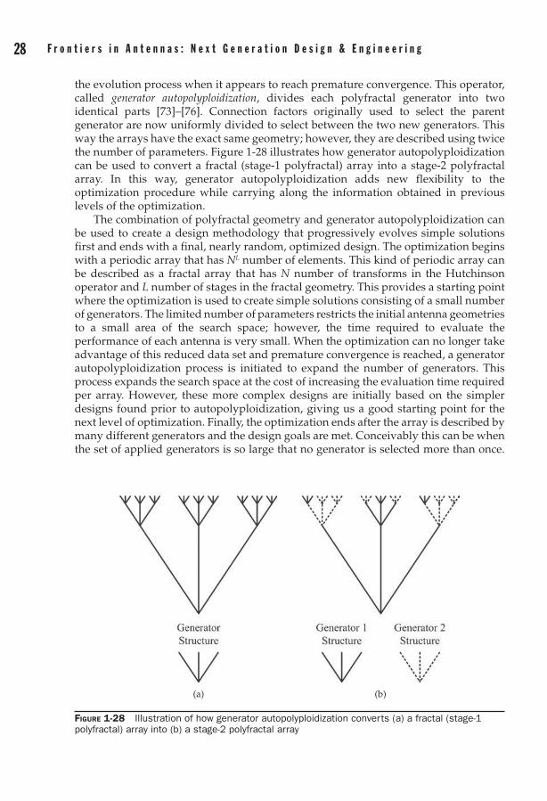
28 F r o n t i e r s i n a n t e n n a s : N e x t G e n e r a t i o n D e s i g n & e n g i n e e r i n g C h a p t e r 1 : U l t r a - W i d e b a n d a n t e n n a a r r a y s 29
the evolution process when it appears to reach premature convergence. This operator, called generator autopolyploidization, divides each polyfractal generator into two identical parts [73]–[76]. Connection factors originally used to select the parent generator are now uniformly divided to select between the two new generators. This way the arrays have the exact same geometry; however, they are described using twice the number of parameters. Figure 1-28 illustrates how generator autopolyploidization can be used to convert a fractal (stage-1 polyfractal) array into a stage-2 polyfractal array. In this way, generator autopolyploidization adds new flexibility to the optimization procedure while carrying along the information obtained in previous levels of the optimization.
The combination of polyfractal geometry and generator autopolyploidization can be used to create a design methodology that progressively evolves simple solutions first and ends with a final, nearly random, optimized design. The optimization begins with a periodic array that has NL number of elements. This kind of periodic array can be described as a fractal array that has N number of transforms in the Hutchinson operator and L number of stages in the fractal geometry. This provides a starting point where the optimization is used to create simple solutions consisting of a small number of generators. The limited number of parameters restricts the initial antenna geometries to a small area of the search space; however, the time required to evaluate the performance of each antenna is very small. When the optimization can no longer take advantage of this reduced data set and premature convergence is reached, a generator autopolyploidization process is initiated to expand the number of generators. This process expands the search space at the cost of increasing the evaluation time required per array. However, these more complex designs are initially based on the simpler designs found prior to autopolyploidization, giving us a good starting point for the next level of optimization. Finally, the optimization ends after the array is described by many different generators and the design goals are met. Conceivably this can be when the set of applied generators is so large that no generator is selected more than once.
Figure 1-28 Illustration of how generator autopolyploidization converts (a) a fractal (stage-1 polyfractal) array into (b) a stage-2 polyfractal array
(a) (b)

28 F r o n t i e r s i n a n t e n n a s : N e x t G e n e r a t i o n D e s i g n & e n g i n e e r i n g C h a p t e r 1 : U l t r a - W i d e b a n d a n t e n n a a r r a y s 29
At this point the polyfractal methodology is used to describe a completely random array. Yet because the polyfractal convention for truly random arrays is cumbersome, the optimization is usually stopped when the disorder of the polyfractal array reaches a sufficiently high enough level. Figure 1-29 illustrates how the optimization procedure progresses and how the array geometry relates to periodic, random, fractal, and polyfractal arrays along the way.
1.3.2 Arrays Based on Raised-Power Series RepresentationsThe concept of the raised-power series (RPS) array design [58] arose after the observation that linear arrays with wide bandwidths and low sidelobe levels tend to have a higher density of elements in the middle of the array with the density tapering off toward the ends. In an attempt to mimic this behavior naturally, the simple array geometry descriptor in (1-39) was created for 2N + 1 element arrays. By controlling the r-parameter, the array adjusts element locations as shown in Fig. 1-30, allowing for various density tapering behavior. The scaling constant in (1-40) is required to maintain a specific minimum element spacing (dmin) for different values of r. For r = 1, the array remains periodic. Normally the range of r is limited to approximately between 0.8 and 1.2 to avoid extremely sparse arrays (especially with large N), which can be undesirable for many applications.
xn = sign(n) ζdmin|n|r for |n| ≤ N (1-39)
ζ( , ) [ ( ) ] ,r N N N r Nr
r r= - - < ≥
≥
-1 1 11 1
1 (1-40)
Figure 1-29 Progression for a typical polyfractal array design optimization. The optimization begins with an initial periodic array geometry described by a fractal. Several generator autopolyploiziation procedures are performed to increase the complexity of the array from a fractal array to a complex polyfractal array. The final optimized array geometry is described by many generators and has a high level of randomness associated with it.
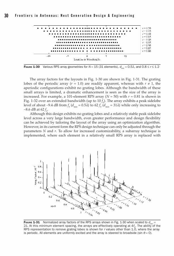
30 F r o n t i e r s i n a n t e n n a s : N e x t G e n e r a t i o n D e s i g n & e n g i n e e r i n g C h a p t e r 1 : U l t r a - W i d e b a n d a n t e n n a a r r a y s 31
The array factors for the layouts in Fig. 1-30 are shown in Fig. 1-31. The grating lobes of the periodic array (r = 1.0) are readily apparent, whereas with r ≠ 1, the aperiodic configurations exhibit no grating lobes. Although the bandwidth of these small arrays is limited, a dramatic enhancement is seen as the size of the array is increased. For example, a 101-element RPS array (N = 50) with r = 0.81 is shown in Fig. 1-32 over an extended bandwidth (up to 10 f0). The array exhibits a peak sidelobe level of about -9.4 dB from f0 (dmin = 0.5l) to 62 f0 (dmin = 31l) while only increasing to -8.6 dB at 62 f0.
Although this design exhibits no grating lobes and a relatively stable peak sidelobe level across a very large bandwidth, even greater performance and design flexibility can be achieved by tailoring the layout of the array using an optimization algorithm. However, in its current form the RPS design technique can only be adjusted through the parameters N and r. To allow for increased customizability, a subarray technique is implemented, where each element in a relatively small RPS array is replaced with
Figure 1-30 Various RPS array geometries for N = 15 (31 elements), dmin
= 0.5l, and 0.8 ≤ r ≤ 1.2
Figure 1-31 Normalized array factors of the RPS arrays shown in Fig. 1-30 when scaled to dmin
= 2l. At this minimum element spacing, the arrays are effectively operating at 4f
0. The ability of the
RPS representation to remove grating lobes is shown for r values other than 1.0, where the array is periodic. All elements are uniformly excited and the array is steered to broadside (sin q = 0).
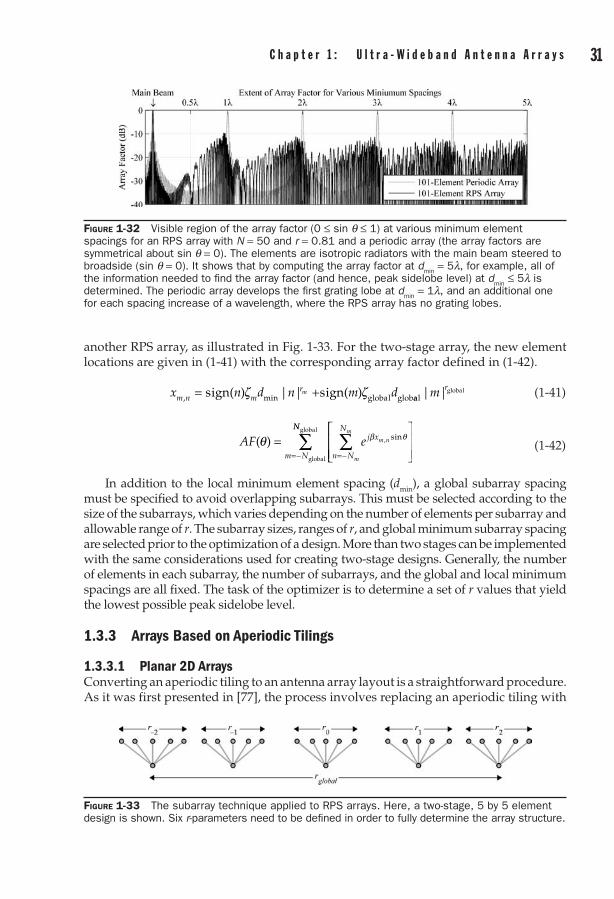
30 F r o n t i e r s i n a n t e n n a s : N e x t G e n e r a t i o n D e s i g n & e n g i n e e r i n g C h a p t e r 1 : U l t r a - W i d e b a n d a n t e n n a a r r a y s 31
another RPS array, as illustrated in Fig. 1-33. For the two-stage array, the new element locations are given in (1-41) with the corresponding array factor defined in (1-42).
x n d n m dm n mrm
, min( ) | | ( )= +sign sign global globζ ζ aalglobal| |m r (1-41)
AF e j x
n N
N
m N
m n
m
m
( ) , sinθ β θ=
=-=-
∑global
NNglobal
∑ (1-42)
In addition to the local minimum element spacing (dmin), a global subarray spacing must be specified to avoid overlapping subarrays. This must be selected according to the size of the subarrays, which varies depending on the number of elements per subarray and allowable range of r. The subarray sizes, ranges of r, and global minimum subarray spacing are selected prior to the optimization of a design. More than two stages can be implemented with the same considerations used for creating two-stage designs. Generally, the number of elements in each subarray, the number of subarrays, and the global and local minimum spacings are all fixed. The task of the optimizer is to determine a set of r values that yield the lowest possible peak sidelobe level.
1.3.3 Arrays Based on Aperiodic Tilings
1.3.3.1 Planar 2D ArraysConverting an aperiodic tiling to an antenna array layout is a straightforward procedure. As it was first presented in [77], the process involves replacing an aperiodic tiling with
Figure 1-32 Visible region of the array factor (0 ≤ sin q ≤ 1) at various minimum element spacings for an RPS array with N = 50 and r = 0.81 and a periodic array (the array factors are symmetrical about sin q = 0). The elements are isotropic radiators with the main beam steered to broadside (sin q = 0). It shows that by computing the array factor at d
min = 5l, for example, all of
the information needed to find the array factor (and hence, peak sidelobe level) at dmin
≤ 5l is determined. The periodic array develops the first grating lobe at d
min = 1l, and an additional one
for each spacing increase of a wavelength, where the RPS array has no grating lobes.
Figure 1-33 The subarray technique applied to RPS arrays. Here, a two-stage, 5 by 5 element design is shown. Six r-parameters need to be defined in order to fully determine the array structure.
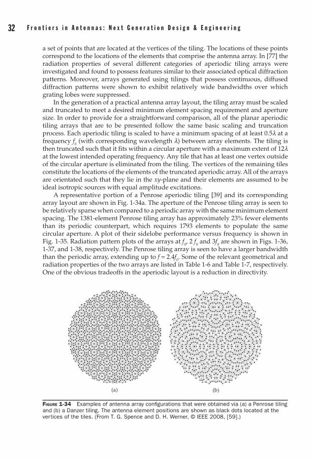
32 F r o n t i e r s i n a n t e n n a s : N e x t G e n e r a t i o n D e s i g n & e n g i n e e r i n g C h a p t e r 1 : U l t r a - W i d e b a n d a n t e n n a a r r a y s 33
a set of points that are located at the vertices of the tiling. The locations of these points correspond to the locations of the elements that comprise the antenna array. In [77] the radiation properties of several different categories of aperiodic tiling arrays were investigated and found to possess features similar to their associated optical diffraction patterns. Moreover, arrays generated using tilings that possess continuous, diffused diffraction patterns were shown to exhibit relatively wide bandwidths over which grating lobes were suppressed.
In the generation of a practical antenna array layout, the tiling array must be scaled and truncated to meet a desired minimum element spacing requirement and aperture size. In order to provide for a straightforward comparison, all of the planar aperiodic tiling arrays that are to be presented follow the same basic scaling and truncation process. Each aperiodic tiling is scaled to have a minimum spacing of at least 0.5l at a frequency f0 (with corresponding wavelength l) between array elements. The tiling is then truncated such that it fits within a circular aperture with a maximum extent of 12l at the lowest intended operating frequency. Any tile that has at least one vertex outside of the circular aperture is eliminated from the tiling. The vertices of the remaining tiles constitute the locations of the elements of the truncated aperiodic array. All of the arrays are orientated such that they lie in the xy-plane and their elements are assumed to be ideal isotropic sources with equal amplitude excitations.
A representative portion of a Penrose aperiodic tiling [39] and its corresponding array layout are shown in Fig. 1-34a. The aperture of the Penrose tiling array is seen to be relatively sparse when compared to a periodic array with the same minimum element spacing. The 1381-element Penrose tiling array has approximately 23% fewer elements than its periodic counterpart, which requires 1793 elements to populate the same circular aperture. A plot of their sidelobe performance versus frequency is shown in Fig. 1-35. Radiation pattern plots of the arrays at f0, 2 f0 and 3f0 are shown in Figs. 1-36, 1-37, and 1-38, respectively. The Penrose tiling array is seen to have a larger bandwidth than the periodic array, extending up to f = 2.4f0. Some of the relevant geometrical and radiation properties of the two arrays are listed in Table 1-6 and Table 1-7, respectively. One of the obvious tradeoffs in the aperiodic layout is a reduction in directivity.
(a) (b)
Figure 1-34 Examples of antenna array configurations that were obtained via (a) a Penrose tiling and (b) a Danzer tiling. The antenna element positions are shown as black dots located at the vertices of the tiles. (From T. G. Spence and D. H. Werner, © IEEE 2008, [59].)

32 F r o n t i e r s i n a n t e n n a s : N e x t G e n e r a t i o n D e s i g n & e n g i n e e r i n g C h a p t e r 1 : U l t r a - W i d e b a n d a n t e n n a a r r a y s 33
A portion of a Danzer aperiodic tiling and its associated antenna array distribution are shown in Fig. 1-34b. The 811-element Danzer array contains significantly fewer elements than the Penrose and periodic arrays; it has approximately 55% fewer elements than the 1793-element periodic array. A plot of the sidelobe performance of the Danzer tiling array and the periodic array is shown in Fig. 1-39. The Danzer array is seen to have the same 2:1 bandwidth as the periodic array, although its sidelobe level within this bandwidth is 4 dB higher. However, it has an extremely wide bandwidth that is void of grating lobes. Contrast this with the conventional periodic array, where grating lobes first appear at a minimum element spacing of 1l. It is noted, however, that even
Table 1-6 Geometrical Properties of the planar aperiodic Tiling Antenna Array Examples. The average minimum nearest neighbor spacing and maximum nearest neighbor spacing correspond to operation at f
0 with a minimum element spacing of 0.5l.
Array Configuration Number of Elements davg dmax
Penrose 1381 0.526l 0.818l
Danzer 811 0.525l 1.123l
Periodic 1793 0.5l 0.5l
Table 1-7 Radiation Properties of the planar aperiodic Tiling Antenna Array Examples. The sidelobe level, half-power beamwidth, and directivity values correspond to operation at f
0 with a minimum
element spacing 0.5l. The bandwidth ratio denotes the ratio of the approximate upper frequency bound of the operating band (SLL < –10 dB) of the array to the lower frequency bound, f
0.
Array Configuration Peak SLL –3 dB Beamwidth Directivity Bandwidth Ratio
Penrose –17.49 dB 2.44° 33.4 dB 2.4:1
Danzer –17.28 dB 2.45° 28.6 dB 2:1
Periodic –17.41 dB 2.46° 34.4 dB 2:1
Figure 1-35 Sidelobe level performance of the Penrose tiling array and a conventional square-lattice periodic array

34 F r o n t i e r s i n a n t e n n a s : N e x t G e n e r a t i o n D e s i g n & e n g i n e e r i n g C h a p t e r 1 : U l t r a - W i d e b a n d a n t e n n a a r r a y s 35
(a) (b)
Figure 1-36 Radiation pattern cuts at (a) j = 0° and (b) j = 90° for the 811-element Danzer tiling array, 1391-element Penrose tiling array, and 1793-element periodic array at f = f
0
Figure 1-37 Radiation pattern cuts at (a) j = 0° and (b) j = 90° for the 811-element Danzer tiling array, 1391-element Penrose tiling array, and 1793-element periodic array at f = 2f
0
(a) (b)
Figure 1-38 Radiation pattern cuts at (a) j = 0° and (b) j = 90° for the 811-element Danzer tiling array, 1391-element Penrose tiling array, and 1793-element periodic array at f = 3f
0
(a) (b)

34 F r o n t i e r s i n a n t e n n a s : N e x t G e n e r a t i o n D e s i g n & e n g i n e e r i n g C h a p t e r 1 : U l t r a - W i d e b a n d a n t e n n a a r r a y s 35
though the Danzer tiling array is void of grating lobes over a very wide bandwidth, its peak sidelobe levels are still relatively high (i.e., greater than -10 dB). Geometrical and radiation properties of the array are listed in Tables 1-6 and 1-7, respectively.
The characteristics of the presented examples are indicative of what would be observed in arrays based on other comparable portions of the tilings, and for the most part, aperiodic tiling arrays in general. In other words, various portions of a tiling tend to generate array layouts with comparable geometrical and performance characteristics. For instance, negligible variations would be observed in the sidelobe level performance of the Danzer array if it had been generated from another portion of the tiling. Similar observations regarding this property of aperiodic tiling arrays were made in [77]. It is worth noting that this property has a propensity to only be associated with moderate to large size arrays since significant variations may be seen among various small tiling arrays.
In their native form, arrays based on the lattices of aperiodic tilings are not well suited for wideband applications, primarily due to their relatively high sidelobes. In addition, the arrays are tied to a particular tiling geometry, which greatly limits their design flexibility. They do however posses some desirable attributes such as grating lobe suppression over a wide bandwidth and the ability to efficiently distribute highly sparse elements across an array aperture. Investigations into these attributes led to the development of a robust design technique that is based on exploiting the geometrical construction properties of aperiodic tilings in the generation of UWB array distributions. Coined recursive-perturbation, this design technique was first discussed in [59]. It employs a simple modification to the basic inflation process whereby additional element locations are efficiently added and controlled through an iterative process: recursive-perturbation. It starts off by placing a point within the boundary of each prototile of an aperiodic set. The locations of these points are preserved within each prototile as a tiling is generated via the inflation process. The result of this process is the formation of an aperiodic tiling that contains an additional point within each of its constituent tiles. Converting this to an array lattice yields elements at the vertices of the tiling as well as an element at each additional perturbation point location. The layout of this tiling array can be readily scaled to obtain a desired minimum element spacing and then truncated to fit within a desired aperture size.
Figure 1-39 Sidelobe level performance of a standard Danzer array and a conventional periodic array
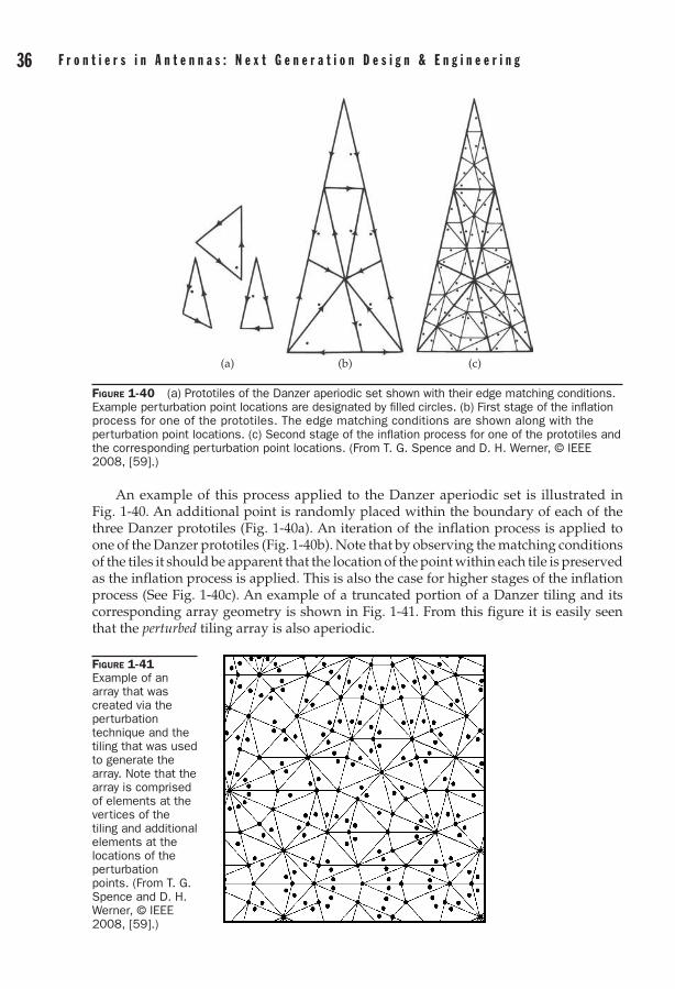
36 F r o n t i e r s i n a n t e n n a s : N e x t G e n e r a t i o n D e s i g n & e n g i n e e r i n g C h a p t e r 1 : U l t r a - W i d e b a n d a n t e n n a a r r a y s 37
An example of this process applied to the Danzer aperiodic set is illustrated in Fig. 1-40. An additional point is randomly placed within the boundary of each of the three Danzer prototiles (Fig. 1-40a). An iteration of the inflation process is applied to one of the Danzer prototiles (Fig. 1-40b). Note that by observing the matching conditions of the tiles it should be apparent that the location of the point within each tile is preserved as the inflation process is applied. This is also the case for higher stages of the inflation process (See Fig. 1-40c). An example of a truncated portion of a Danzer tiling and its corresponding array geometry is shown in Fig. 1-41. From this figure it is easily seen that the perturbed tiling array is also aperiodic.
Figure 1-40 (a) Prototiles of the Danzer aperiodic set shown with their edge matching conditions. Example perturbation point locations are designated by filled circles. (b) First stage of the inflation process for one of the prototiles. The edge matching conditions are shown along with the perturbation point locations. (c) Second stage of the inflation process for one of the prototiles and the corresponding perturbation point locations. (From T. G. Spence and D. H. Werner, © IEEE 2008, [59].)
(a) (b) (c)
Figure 1-41 Example of an array that was created via the perturbation technique and the tiling that was used to generate the array. Note that the array is comprised of elements at the vertices of the tiling and additional elements at the locations of the perturbation points. (From T. G. Spence and D. H. Werner, © IEEE 2008, [59].)
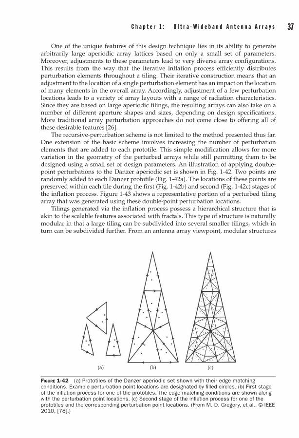
36 F r o n t i e r s i n a n t e n n a s : N e x t G e n e r a t i o n D e s i g n & e n g i n e e r i n g C h a p t e r 1 : U l t r a - W i d e b a n d a n t e n n a a r r a y s 37
One of the unique features of this design technique lies in its ability to generate arbitrarily large aperiodic array lattices based on only a small set of parameters. Moreover, adjustments to these parameters lead to very diverse array configurations. This results from the way that the iterative inflation process efficiently distributes perturbation elements throughout a tiling. Their iterative construction means that an adjustment to the location of a single perturbation element has an impact on the location of many elements in the overall array. Accordingly, adjustment of a few perturbation locations leads to a variety of array layouts with a range of radiation characteristics. Since they are based on large aperiodic tilings, the resulting arrays can also take on a number of different aperture shapes and sizes, depending on design specifications. More traditional array perturbation approaches do not come close to offering all of these desirable features [26].
The recursive-perturbation scheme is not limited to the method presented thus far. One extension of the basic scheme involves increasing the number of perturbation elements that are added to each prototile. This simple modification allows for more variation in the geometry of the perturbed arrays while still permitting them to be designed using a small set of design parameters. An illustration of applying double-point perturbations to the Danzer aperiodic set is shown in Fig. 1-42. Two points are randomly added to each Danzer prototile (Fig. 1-42a). The locations of these points are preserved within each tile during the first (Fig. 1-42b) and second (Fig. 1-42c) stages of the inflation process. Figure 1-43 shows a representative portion of a perturbed tiling array that was generated using these double-point perturbation locations.
Tilings generated via the inflation process possess a hierarchical structure that is akin to the scalable features associated with fractals. This type of structure is naturally modular in that a large tiling can be subdivided into several smaller tilings, which in turn can be subdivided further. From an antenna array viewpoint, modular structures
Figure 1-42 (a) Prototiles of the Danzer aperiodic set shown with their edge matching conditions. Example perturbation point locations are designated by filled circles. (b) First stage of the inflation process for one of the prototiles. The edge matching conditions are shown along with the perturbation point locations. (c) Second stage of the inflation process for one of the prototiles and the corresponding perturbation point locations. (From M. D. Gregory, et al., © IEEE 2010, [78].)
(a) (b) (c)

38 F r o n t i e r s i n a n t e n n a s : N e x t G e n e r a t i o n D e s i g n & e n g i n e e r i n g C h a p t e r 1 : U l t r a - W i d e b a n d a n t e n n a a r r a y s 39
can often be utilized to provide simplified construction as well as a convenient subarray architecture [35], [40]. By judicious selection of a portion of an aperiodic tiling, the potential exists for a highly modular array design that is comprised of a collection of several identical subarrays. And if care is taken, modularity can be preserved in designs that are generated using the tiling perturbation technique.
1.3.3.2 Volumetric 3D ArraysIn the case of volumetric aperiodic tiling arrays, the conversion from a tiling to antenna array follows the same basic process that was outlined for planar tiling arrays. Once the arrays are generated, in order to steer the main beam in a given direction, the excitation current phases of the elements must be set according to
bn = –krn [sin q0 sin qn cos(j0 – jn) + cos q0 cosqn] (1-43)
where k is the wavenumber, rn, qn, and jn are the spherical coordinates of the nth element, and q0 and f0 correspond to the direction of the main beam.
Similar to the planar aperiodic arrays, the radiation patterns of the volumetric aperiodic arrays do not develop any grating lobes when the minimum element spacing is increased beyond one wavelength. To compare the performance of the Danzer aperiodic volumetric array with a uniform periodic array, we consider a 3D spherical distribution of elements with a radius and minimum spacing of 5l, and 0.5l, respectively. The resulting periodic array has 4169 elements. The aperiodic array is considerably thinned and has 575 elements. The radiation pattern for the periodic and aperiodic arrays with main beam steered to q0 = 0 and j0 = 0 at frequency f = f0 are shown in Figs. 1-44a and 1-44b, respectively. As can be seen from the plots, even with a minimum element spacing of 0.5l, the periodic array has a grating lobe, whereas the aperiodic array has no grating lobes and a peak sidelobe level of roughly –13 dB.
Figure 1-43 Example of an array that was created via two perturbation points per prototile and its corresponding tiling. Note that the array is comprised of elements at the vertices of the tiling and additional elements at the locations of the perturbation points. The element locations correspond to those shown in Figure 1-42. (From M. D. Gregory, et al., © IEEE 2010, [78].)
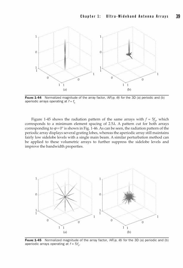
38 F r o n t i e r s i n a n t e n n a s : N e x t G e n e r a t i o n D e s i g n & e n g i n e e r i n g C h a p t e r 1 : U l t r a - W i d e b a n d a n t e n n a a r r a y s 39
Figure 1-45 shows the radiation pattern of the same arrays with f = 5f0, which corresponds to a minimum element spacing of 2.5l. A pattern cut for both arrays corresponding to j = 0° is shown in Fig. 1-46. As can be seen, the radiation pattern of the periodic array displays several grating lobes, whereas the aperiodic array still maintains fairly low sidelobe levels with a single main beam. A similar perturbation method can be applied to these volumetric arrays to further suppress the sidelobe levels and improve the bandwidth properties.
1
0
11
0
1 1
0
1
1
0
11
0
1 1
0
1
(a) (b)
Figure 1-44 Normalized magnitude of the array factor, |AF(j, q)| for the 3D (a) periodic and (b) aperiodic arrays operating at f = f
0
Figure 1-45 Normalized magnitude of the array factor, |AF(f, q)| for the 3D (a) periodic and (b) aperiodic arrays operating at f = 5f
0.
1
0
11
0
1 1
0
1
1
0
11
0
1 1
0
1
(a) (b)

40 F r o n t i e r s i n a n t e n n a s : N e x t G e n e r a t i o n D e s i g n & e n g i n e e r i n g C h a p t e r 1 : U l t r a - W i d e b a n d a n t e n n a a r r a y s 41
1.4 UWB Array Design ExamplesThe previous sections discussed various design techniques for generating wideband and UWB array distributions. They covered aperiodic linear and planar array distributions as well as techniques for 3D volumetric array design. This section presents several examples that will highlight the capabilities of the aforementioned UWB array design techniques. In particular, designs will be presented for relatively small arrays of 32 elements up to arrays with large element counts of nearly 2,000. The main objective of these designs is to eliminate grating lobes and to achieve sidelobe suppression (usually -10 dB or better) over a prescribed bandwidth. Nevertheless, some of the proposed techniques have been used to optimize designs that meet this objective in addition to other useful array attributes, such as thinning distributions (percentage of thinned elements in a given aperture), targeting a particular directivity, and targeting a particular half-power beamwidth.
1.4.1 Linear and Planar Polyfractal Array ExamplesIn this section, several examples of linear and planar UWB polyfractal arrays are presented. All of the examples were designed using a Pareto-based multiobjective optimization with the goal of tailoring operation at two widely spaced frequencies. As will be shown, in many cases very wide bandwidths of suppressed sidelobes are attained even though the design process only focused on optimizing performance at two frequencies within the lower range of the operating bandwidth. The designs that will be shown assume the arrays are comprised of isotropic radiators with uniform amplitude excitations. Moreover, all of the designs targeted broadside operation, though the potential for excellent beam steering capabilities naturally results from the very wide bandwidths of the designs.
Figure 1-46 Cut of array factor for the 3D (a) periodic array and (b) aperiodic array at f = 0° and f = 5f
0.
0
–5
–10
–15
–20
–25
–30
–35
–40–100 100
θ (degrees) θ (degrees)
0
0
–5
–10
–15
–20
–25
–30
–35
–40–100 1000
Arr
ay F
acto
r (d
B)
Arr
ay F
acto
r (d
B)
(a) (b)

40 F r o n t i e r s i n a n t e n n a s : N e x t G e n e r a t i o n D e s i g n & e n g i n e e r i n g C h a p t e r 1 : U l t r a - W i d e b a n d a n t e n n a a r r a y s 41
The first example that is shown is based on simultaneously minimizing the peak sidelobes of a 32-element linear polyfractal array for operation corresponding to minimum element spacings of 0.5l and 2l (i.e., for two different widely separated operating frequencies f0 and 4f0). The optimization of the array was based on an initial population consisting of a pool of randomly perturbed two-generator polyfractal arrays derived from a 32-element periodic array. The optimization process was carried out through 600 generations, with generator autopolyploidizations stimulating the evolution of the design by doubling the number of generators at generations 150, 300, and 450. Figure 1-47 illustrates the evolution of the Pareto front over the 600 generations considered in this design.
The Pareto front from the final generation of the optimization is illustrated in Fig. 1-48. This front consists of many different polyfractal array solutions, each possessing 32 elements. As shown in this figure, the population members along the Pareto front present various trade-offs in the design objectives. The two Pareto front
0
200
100
300
400
500
6000
24
68
1012
1416
1820 12
108
64
20
Gen
erat
ion
SLL at 0.5λ minimum spacing SLL at 2.0λ minimum spacing
Figure 1-47 Evolution of the Pareto front over time. The final Pareto front consists of solutions possessing 32 elements. The black rings around the plot indicate the occurrence of an autopolyploidization process at generations 150, 300, and 450.

42 F r o n t i e r s i n a n t e n n a s : N e x t G e n e r a t i o n D e s i g n & e n g i n e e r i n g C h a p t e r 1 : U l t r a - W i d e b a n d a n t e n n a a r r a y s 43
members that appeared to possess the best balance in the design objectives are denoted in the figure. One of the selected designs (array A) has the best sidelobe performance at f = 4f0. The other (array B) has a slightly higher sidelobe level at f = 4f0 but a significantly lower level at f = f0. The performance properties of these two arrays are summarized in Table 1-8. A comparison of the sidelobe performance of these designs, along with that of a 32-element periodic array, is shown in Fig. 1-49. In Section 1.5.3, the 32-element polyfractal designs will be further examined through experimental verification.
Even though the design of the polyfractal arrays only focused on optimizing performance at the frequencies of f0 and 4f0, the resulting designs possess a very wide bandwidth with no grating lobes and suppressed sidelobes. This desirable feature is also noted for a number of the examples that will be presented in the remainder of this section. Since evaluating arrays at a large minimum element spacing (higher frequency) requires more time than a smaller element spacing, this can be useful for obtaining very wide bandwidth arrays in a relatively short amount of time.
The methodology used to create the relatively small 32-element polyfractal arrays can be easily applied to the design of arrays with much higher element counts. For instance, the following example involves designing an UWB polyfractal array with nearly 2000 elements. The design objective was similar to that of the preceding example: sidelobes are to be minimized at minimum element spacings of 0.5l and 3l (i.e., for operating frequencies f0 and 6f0). In this case the initial population consisted of a pool of randomly perturbed two-generator polyfractal arrays derived from a 2401-element periodic array. The design was evolved over 500 generations, with generator autopolyploidizations doubling the number of generators at generations 82 and 221. Figure 1-50 illustrates the evolution of the Pareto front throughout the optimization.
Figure 1-48 Final Pareto front (where SLL is the peak sidelobe level) of the 32-element polyfractal array optimization with chosen members highlighted [79]
Minimum Spacing f/f
o
Average Spacing
Peak Sidelobe
–3 dB Beamwidth Directivity
Array A0.5l 1 0.80l –13.70 dB 1.28° 15.69 dB
2.0l 4 3.19l –10.02 dB 0.32° 15.07 dB
Array B0.5l 1 0.68l –17.65 dB 1.54° 16.01 dB
2.0l 4 2.74l –9.52 dB 0.39° 15.00 dB
Table 1-8 Performance Properties for the 32-Element GA Optimized Linear Arrays

42 F r o n t i e r s i n a n t e n n a s : N e x t G e n e r a t i o n D e s i g n & e n g i n e e r i n g C h a p t e r 1 : U l t r a - W i d e b a n d a n t e n n a a r r a y s 43
Figure 1-49 Sidelobe level performance of the 32-element polyfractal arrays (designs A and B) and a 32-element periodic array. The array elements are uniformly excited and assumed to be isotropic radiators.
0
50
100
150
200
250
300
350
400
450
5008
1012
1416
1820
2224 26
2422
2018
1614
1210
Gen
erat
ion
SLL at 0.5λ minimum spacing SLL at 3.0λ minimum spacing
Figure 1-50 Evolution of the Pareto front over time. The final Pareto front consists of solutions possessing between 1958 and 1960 elements. The black rings around the plot indicate the occurrence of an autopolyploidization process at generations 82 and 221 [80].
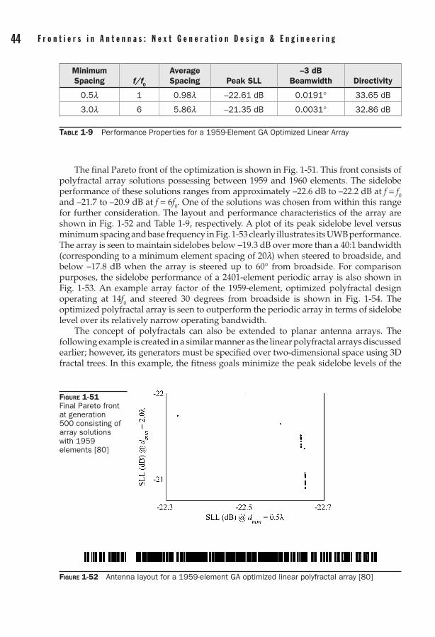
44 F r o n t i e r s i n a n t e n n a s : N e x t G e n e r a t i o n D e s i g n & e n g i n e e r i n g C h a p t e r 1 : U l t r a - W i d e b a n d a n t e n n a a r r a y s 45
The final Pareto front of the optimization is shown in Fig. 1-51. This front consists of polyfractal array solutions possessing between 1959 and 1960 elements. The sidelobe performance of these solutions ranges from approximately –22.6 dB to –22.2 dB at f = f0 and –21.7 to –20.9 dB at f = 6f0. One of the solutions was chosen from within this range for further consideration. The layout and performance characteristics of the array are shown in Fig. 1-52 and Table 1-9, respectively. A plot of its peak sidelobe level versus minimum spacing and base frequency in Fig. 1-53 clearly illustrates its UWB performance. The array is seen to maintain sidelobes below -19.3 dB over more than a 40:1 bandwidth (corresponding to a minimum element spacing of 20l) when steered to broadside, and below –17.8 dB when the array is steered up to 60° from broadside. For comparison purposes, the sidelobe performance of a 2401-element periodic array is also shown in Fig. 1-53. An example array factor of the 1959-element, optimized polyfractal design operating at 14f0 and steered 30 degrees from broadside is shown in Fig. 1-54. The optimized polyfractal array is seen to outperform the periodic array in terms of sidelobe level over its relatively narrow operating bandwidth.
The concept of polyfractals can also be extended to planar antenna arrays. The following example is created in a similar manner as the linear polyfractal arrays discussed earlier; however, its generators must be specified over two-dimensional space using 3D fractal trees. In this example, the fitness goals minimize the peak sidelobe levels of the
Figure 1-51 Final Pareto front at generation 500 consisting of array solutions with 1959 elements [80]
Figure 1-52 Antenna layout for a 1959-element GA optimized linear polyfractal array [80]
Table 1-9 Performance Properties for a 1959-Element GA Optimized Linear Array
Minimum Spacing f/f0
Average Spacing Peak SLL
–3 dB Beamwidth Directivity
0.5l 1 0.98l –22.61 dB 0.0191° 33.65 dB
3.0l 6 5.86l –21.35 dB 0.0031° 32.86 dB

44 F r o n t i e r s i n a n t e n n a s : N e x t G e n e r a t i o n D e s i g n & e n g i n e e r i n g C h a p t e r 1 : U l t r a - W i d e b a n d a n t e n n a a r r a y s 45
array for minimum element spacings of 0.5l and 2l (i.e., for operating frequencies f0 and 4f0). The initial population consists of a pool of randomly perturbed single-generator polyfractal arrays derived from an initial 343-element planar array that is based on a triangular lattice with an aperture bounded by the shape of a Koch-snowflake [41]. The optimized design was evolved through 200 generations, with a generator autopolyploidization doubling the number of generators after 86 generations. Figure 1-55 illustrates the evolution of the Pareto front over these 200 generations.
Again, one solution is chosen from the Pareto front for further consideration. This selected solution has 343-elements and a peak sidelobe level of -15.7 dB and -13.9 dB for operation corresponding to minimum element spacings of 0.5l and 2.0l, respectively. The layout of the array is shown in Fig. 1-56. The aperture of this array is similar to that of the array used to seed the optimization. However, there is noticeable deviation from a triangular lattice in its interior layout. The performance characteristics of the array are
Figure 1-53 Sidelobe level performance of the optimized 1959-element polyfractal array and a comparable periodic linear array over a range of frequencies and element spacings. The solid lines correspond to broadside operation while the dashed lines represent the operation of an array steered 60° from broadside. The polyfractal array was optimized for broadside operation at f = f
0 and 6f
0 (corresponding to element spacings of 0.5l and 3l) [80].
Figure 1-54 The Radiation pattern of the 1959-element optimized polyfractal array operating at a frequency of 14f
0 steered to -30°. This array possesses a peak sidelobe level of -19.28 dB.
The right side of the figure illustrates the entire radiation pattern while the left side of the figure shows more detail in the region of the main beam at -30°.
0
–10
–20
–30
–40–30.02 –30.01 –30 –29.99 –29.98 –90 –60 –30 0 30 60 90
Theta (degrees)
Arr
ay F
acto
r (d
B)
–19.28

46 F r o n t i e r s i n a n t e n n a s : N e x t G e n e r a t i o n D e s i g n & e n g i n e e r i n g C h a p t e r 1 : U l t r a - W i d e b a n d a n t e n n a a r r a y s 47
0
20
40
60
80
100
120
140
160
180
2000 0
2 24 46 68 8
10 1012 1214 14
16 1618 18
20 20
Gen
erat
ion
SLL at 0.5λ minimum spacing SLL at 2.0λ minimum spacing
Figure 1-55 Evolution of the Pareto front over time. The final Pareto front consists of solutions possessing between 319 and 343 elements. The black ring around the plot indicates the occurrence of an autopolyploidization process at generation 86.
Figure 1-56 Antenna layout for a 343-element GA optimized planar polyfractal array

46 F r o n t i e r s i n a n t e n n a s : N e x t G e n e r a t i o n D e s i g n & e n g i n e e r i n g C h a p t e r 1 : U l t r a - W i d e b a n d a n t e n n a a r r a y s 47
summarized in Table 1-10 and a plot of its sidelobe performance versus minimum spacing and base frequency is shown in Fig. 1-57. The array is seen to maintain an ultra-wide bandwidth with no grating lobes and excellent sidelobe suppression up to operation of at least a minimum element spacing of 20l (corresponding to a bandwidth of at least 40:1), even when steered up to 60° from broadside. For comparison purposes its performance is shown along with that of a 400-element square-lattice periodic array (with a square aperture). Example array factors of the optimized design operating at 4f0 and 12f0 are shown in Fig. 1-58.
1.4.2 Linear RPS Array Design ExamplesThis section presents several examples of linear RPS arrays designed for UWB performance [58]. Examples will be shown for two- and three-stage RPS arrays, which range in size from 55 elements to slightly more than 1,000 elements. As will be shown, and as expected, the largest bandwidth and greatest sidelobe suppression comes about from larger RPS arrays. The goal of all the presented examples was to minimize the peak sidelobe level over a 20:1 bandwidth. This was accomplished by minimizing the sidelobe level at a frequency of 20f0, where the minimum element spacing is restricted to be equal to 10l. The array design was carried out using a genetic algorithm. All of the arrays are assumed to be comprised of uniformly excited, isotropic elements.
Table 1-10 Performance Properties for a 343-Element GA Optimized Planar Polyfractal Array
Minimum Spacing f/f
o
Average Area per Element Peak SLL
–3 dB Beamwidth
DirectivityMin. Max.
0.5l 1 0.92l2 –15.68 dB 2.62° 2.63° 28.49 dB
2.0l 4 3.68l2 –13.89 dB 0.65° 0.65° 25.89 dB
Figure 1-57 Sidelobe level performance for the optimized 343-element polyfractal array over a range of bandwidth compared to the performance of a periodic planar array. The solid lines correspond to broadside operation while the dashed lines represent the operation of an array steered 60° from broadside. The polyfractal array is optimized at broadside for simultaneous operation at two frequencies corresponding to minimum element spacings of 0.5l and 2l (i.e., f0 and 4f
0).

48 F r o n t i e r s i n a n t e n n a s : N e x t G e n e r a t i o n D e s i g n & e n g i n e e r i n g C h a p t e r 1 : U l t r a - W i d e b a n d a n t e n n a a r r a y s 49
The first example is a relatively small two-stage design, with five subarrays of 11 elements each. Like the example in Fig. 1-33, this design required six parameters for complete array representation. The global subarray parameter was limited to 0.8 ≤ r ≤ 1.2 and each subarray parameter was limited to the range of 0.75 ≤ r ≤ 1.16. A genetic algorithm was used to find the best set of parameters that results in the lowest peak relative sidelobe level at dmin = 10l. A population of 120 members was selected and permitted to run for 500 generations (60k total array evaluations). The optimization performance of the GA for this design problem is shown in Fig. 1-59. The array layout of the best design is shown in Fig. 1-60, with the array factors at dmin = 0.5l and 10l shown in Figs. 1-61 and 1-62, respectively. The performance of the array over an extended bandwidth is given in Fig. 1-72.
The same optimization process was carried out for three additional RPS array designs. They are based on a larger number of elements and a greater number of subarrays.
90
45
0
f = 4
f o (2
λ m
in. s
paci
ng)
–45
–90–90 –45 0
Top View
45 90(a)
0
–5
–10
–20
–15
–25
–30
–35
–40–90 –45 0
Side View
45 90(b)
90
45
0
–45
–90–90 –45 0 45 90
f = 1
2 f o
(6 λ
min
. spa
cing
)
(c)
0
–5
–10
–20
–15
–25
–30
–35
–40–90 –45 0 45 90
(d)
Figure 1-58 Radiation pattern for the 343-element planar polyfractal array operating at frequencies of 4f
0 and 12f
0. At these frequencies this array possesses a peak sidelobe level of -13.9 dB and
-13.6 dB, respectively, without the occurrence of grating lobes.

48 F r o n t i e r s i n a n t e n n a s : N e x t G e n e r a t i o n D e s i g n & e n g i n e e r i n g C h a p t e r 1 : U l t r a - W i d e b a n d a n t e n n a a r r a y s 49
Figure 1-59 Evolution of the best performing array throughout the genetic algorithm evolution of the two-stage 55-element RPS array. The final optimized design has a peak sidelobe level of -9.58 dB at a minimum element spacing of 10l (f = 20f
0).
Figure 1-60 Element locations for the optimized, two-stage 55-element RPS array. Note that the grouping effect of the subarray method is easily identified in the array layout.
Figure 1-61 Normalized array factor of the optimized, two-stage 55-element RPS array at a minimum element spacing of 0.5l. At this element spacing the array has a peak sidelobe level of -13.5 dB. This level is lower than that of a comparable linear periodic array.
Figure 1-62 Normalized array factor of the optimized, two-stage, RPS array of 55 elements at d
min = 10l. The array exhibits no grating lobes and maintains good sidelobe level suppression up
to a 20:1 frequency bandwidth. The peak sidelobe level of the array is -9.58 dB.

50 F r o n t i e r s i n a n t e n n a s : N e x t G e n e r a t i o n D e s i g n & e n g i n e e r i n g C h a p t e r 1 : U l t r a - W i d e b a n d a n t e n n a a r r a y s 51
In addition, some of the examples are based on increasing the number of stages in the array. It will be shown that their performance far exceeds that of the first example. In each case the array bandwidth exceeds 80:1. The performance characteristics of all of the designs in this section are summarized in Table 1-11.
The first example in this set is a two-stage RPS design based on 21 subarrays of 21 elements each, with a total size of 441 elements. Its architecture contains 22 parameters that are to be optimized by the genetic algorithm: its global r-parameter is limited to the range of 0.8 ≤ r ≤ 1.2 and its local r-parameters for the 21 subarrays are limited to 0.71 ≤ r ≤ 1.14. The global subarray spacing was specified to be dglobal = 14.955l, which leaves enough room for a spacing of 0.5l between neighboring subarrays at the lowest intended operating frequency. The layout of the optimized array is shown in Fig. 1-63. This array has a peak sidelobe level below -15 dB at the targeted design frequency of 20f0 and it maintains a level below –14 dB over at least an 80:1 bandwidth. Cuts of its radiation pattern are shown in Figures 1-64 and 1-65 for operation corresponding to a minimum element spacing of 0.5l and 10l, respectively. A plot of its sidelobe performance versus element spacing and frequency is shown in Fig. 1-72.
Figure 1-63 Element locations of the 441-element, optimized, two-stage RPS array
Figure 1-64 Normalized array factor of the 441-element, optimized, two-stage RPS array at a minimum element spacing of 0.5l (f = f
0). The peak sidelobe level of the array is -15.0 dB.
Figure 1-65 Normalized array factor of the 441-element, optimized, two-stage RPS array at a minimum element spacing of 10l (f = 20f
0). The peak sidelobe level of the array is -15.0 dB.
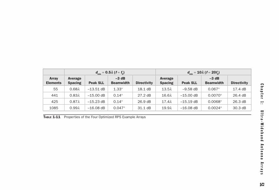
50
Frontiers in a
ntennas: N
ext Generatio
n Design &
engineerin
g
Chapter 1:
Ultra-W
ideband antenna a
rrays 51
dmin = 0.5l (f = f0) dmin = 10l (f = 20f0)
Array Elements
Average Spacing Peak SLL
–3 dB Beamwidth Directivity
Average Spacing Peak SLL
–3 dB Beamwidth Directivity
55 0.68l –13.51 dB 1.33° 18.1 dB 13.5l –9.58 dB 0.067° 17.4 dB
441 0.83l –15.00 dB 0.14° 27.2 dB 16.6l –15.00 dB 0.0070° 26.4 dB
425 0.87l –15.23 dB 0.14° 26.9 dB 17.4l –15.19 dB 0.0068° 26.3 dB
1085 0.99l –16.08 dB 0.047° 31.1 dB 19.9l –16.08 dB 0.0024° 30.3 dB
Table 1-11 Properties of the Four Optimized RPS Example Arrays

52 F r o n t i e r s i n a n t e n n a s : N e x t G e n e r a t i o n D e s i g n & e n g i n e e r i n g C h a p t e r 1 : U l t r a - W i d e b a n d a n t e n n a a r r a y s 53
Next, a three-stage array was designed using nearly the same number of elements as the previous two-stage design. Here, a 5 by 5 by 17 (425 total) element array was optimized, requiring 31 parameters for full representation. All of the controlling r-parameters were limited to the range of 0.71 ≤ r ≤ 1.14. The optimization required 300 generations with a population size of 120 members to reach a peak relative sidelobe level of -15.2 dB at a minimum element spacing of 10l. The element locations of the optimized design are shown in Fig. 1-66. The array factors of the optimized design at 0.5l and 10l minimum element spacing are shown in Figs. 1-67 and 1-68, respectively. The performance of the array over an extended bandwidth is shown in Fig. 1-72.
The final example is an even larger three-stage RPS array. It is based on a 5 by 7 by 31 RPS configuration (1085 elements in total). This array possesses 41 parameters that can be used to control its overall layout. Once again, all of the controlling r-parameters were limited to a range of 0.71 ≤ r ≤ 1.14. The optimization of this RPS array resulted in the layout shown in Fig. 1-69. A plot of its sidelobe performance versus minimum element spacing and frequency is shown in Fig. 1-72. At the targeted design frequency
Figure 1-66 Element locations of the 425-element, optimized, three-stage RPS array
Figure 1-67 Normalized array factor of the 425-element, optimized, three-stage RPS array at a minimum element spacing of 0.5l (f = f
0). The peak sidelobe level of the array is -15.23 dB.
Figure 1-68 Normalized array factor of the 425-element, optimized, three-stage RPS array at a minimum element spacing of 10l (f = 20f
0). The peak sidelobe level of the array is -15.19 dB.

52 F r o n t i e r s i n a n t e n n a s : N e x t G e n e r a t i o n D e s i g n & e n g i n e e r i n g C h a p t e r 1 : U l t r a - W i d e b a n d a n t e n n a a r r a y s 53
the array has a peak sidelobe level of -16 dB. This level is maintained over at least an 80:1 bandwidth. In terms of sidelobe suppression its performance far surpasses that of the smaller polyfractal array designs and the baseline linear periodic array. Representative cuts of the array factor for the optimized array are shown in Figs. 1-70 and 1-71 for minimum element spacings of 0.5l and 10l, respectively.
1.4.3 Planar Array Examples Based on Aperiodic TilingsThis section will demonstrate the effectiveness of the recursive-perturbation design technique for aperiodic tiling arrays through the presentation of a few design examples. The first is based on applying single-point perturbations to a Danzer aperiodic tiling. As an extension of this, the second example applies double-point perturbations to the same tiling, resulting in greater design control and bandwidth enhancement. Finally, an example will be shown for an array designed using a dynamic perturbation scheme
Figure 1-69 Element locations of the 1085-element, optimized, three-stage RPS array
Figure 1-70 Normalized array factor of the 1085-element, optimized, three-stage RPS array at a minimum element spacing of 0.5l (f = f
0). The peak sidelobe level of the array is -16.08 dB.
Figure 1-71 Normalized array factor of the 1085-element, optimized, three-stage RPS array at a minimum element spacing of 10l (f = 20f
0). The peak sidelobe level of the array is -16.08 dB.

54 F r o n t i e r s i n a n t e n n a s : N e x t G e n e r a t i o n D e s i g n & e n g i n e e r i n g C h a p t e r 1 : U l t r a - W i d e b a n d a n t e n n a a r r a y s 55
that permits the number of perturbations points to vary per prototile. This modification led to a design with more than a 60:1 bandwidth with no grating lobes and suppressed sidelobes.
All of the presented designs were restricted to have the same general aperture shape and size. This was fixed to match the designs shown in Fig. 1-34. However, since the array distributions are simply based on truncated portions of a very large tiling, designs with alternate aperture shapes and sizes could readily be generated to meet specific requirements. For instance, it is a simple process to convert the presented designs to fit within an alternate aperture such as a circle, ellipse, or some other more complicated 2D shape. Similar to other arrays presented in this chapter, the arrays in this section were designed to have a minimum element spacing of l/2 at the lowest intended operating frequency, f0 (with associated wavelength l). This spacing was chosen for convenience. It will be shown that the large bandwidth of an UWB lattice permits flexibility in the spacing at the lowest operating frequency. All of the design results presented here assume that the arrays are comprised of uniformly excited isotropic radiators.
The first example involves a perturbed Danzer tiling array that was designed for maximum sidelobe suppression at f = 10f0, corresponding to a minimum element spacing of 5l. This example utilizes a single-point perturbation within each of the three Danzer prototiles. This accounts for a total of six design parameters (x,y coordinates for each perturbation point). A GA was used to determine the optimal set of perturbation locations subject to the design objective. A standard, unperturbed Danzer tiling array (see Fig. 1-34b) and a square-lattice periodic array were used as a baseline for comparison with the perturbed array. Their sidelobe level performance versus frequency is shown in Fig. 1-74. At f = 10f0, the Danzer tiling array has a sidelobe level of –2.2 dB and the periodic array has a peak lobe level of 0 dB due to the numerous grating lobes in its radiation pattern.
Figure 1-72 Peak sidelobe level performance of the four example arrays over an extended bandwidth along with a standard periodic array. All elements are uniformly excited and steered to broadside.

54 F r o n t i e r s i n a n t e n n a s : N e x t G e n e r a t i o n D e s i g n & e n g i n e e r i n g C h a p t e r 1 : U l t r a - W i d e b a n d a n t e n n a a r r a y s 55
The GA optimization resulted in an array design, (shown in Fig. 1-73) with excellent sidelobe suppression over an ultra-wide bandwidth. At f = 10f0 the sidelobe level was reduced from –2.2 dB to –10.05 dB and the upper bound on the bandwidth of the array was extended from f = 2f0 to f = 10.5f0. This corresponds to a bandwidth enhancement from 2:1, in the case of the standard Danzer array, to 10.5:1 for the perturbed design. Figure 1-74 provides a plot of the sidelobe level performance of the optimized design as well as that of the standard Danzer array and the periodic array. In terms of sidelobe suppression, the perturbed design is seen to outperform the standard Danzer array over nearly the entire domain of the plot. A representative cut of its radiation pattern at the optimized frequency is shown in Fig. 1-75 and some of the geometrical and radiation characteristics of the array are listed in Table 1-12.
Figure 1-73 Element distribution of the 811-element, single-point perturbed Danzer aperiodic tiling array that was designed for operation at f = 10f
o(From T. G.
Spence and D. H. Werner, © IEEE 2008, [59])
Figure 1-74 Sidelobe level performance of the 811-element, single-point perturbed Danzer aperiodic tiling array, an unperturbed 811-element Danzer aperiodic tiling array, and a 1,793-element square-lattice periodic array. All of the arrays fit within a circular aperture with a radius of 12l (with a minimum element spacing of 0.5l at the lowest intended operating frequency).

56 F r o n t i e r s i n a n t e n n a s : N e x t G e n e r a t i o n D e s i g n & e n g i n e e r i n g C h a p t e r 1 : U l t r a - W i d e b a n d a n t e n n a a r r a y s 57
The goal of this example was to suppress sidelobes at the upper bound of a targeted bandwidth. This ensures that the sidelobes at all lower frequencies will be equal to or less than that of the upper bound. While this objective is well suited for achieving wideband performance, it does not place any consideration on the specific degree of sidelobe suppression at lower operating frequencies. In this case the array is seen to have a relatively steady sidelobe level over a majority of its bandwidth; from f = 2.5f0 up to the upper bound of f = 10.4f0 there is approximately a decibel of deviation in its sidelobe level (see Fig. 1-74). Incorporating an additional sampling frequency into the design process provides the potential for tailored sidelobe suppression over specific regions in the bandwidth of an array. In the case of aperiodic tiling arrays, this dual-frequency approach combined with the flexibility of the perturbation technique allows for significant improvements in the sidelobe suppression at lower frequencies of UWB designs.
Figure 1-75 Radiation pattern cut at f = 10f0 for the single-point perturbed Danzer aperiodic tiling
array. The right side of the figure shows the array factor as a function of theta plotted from -90° to +90°, and the left side of the figure shows a detailed view of the array factor near the main beam. (From T. G. Spence and D. H. Werner, © IEEE 2008, [59].)
Array Type BandwidthPeak SLL @ Bandwidth Directivity
–3 dB Beamwidth davg dmax
811-Element Single Point Perturbed Danzer
10.4:1 –10.05 dB 31.26 dB 2.43° 0.57l 1.17l
678-Element Dual Point Perturbed Danzer
22.7:1 –11.13 dB 30.6 dB 2.44° 0.63l 1.28l
518-Element Three and Four Point Perturbed Danzer
63:1 –10.77 dB 27.16 dB 2.32° 0.68l 1.65l
Table 1-12 Characteristics of the Optimized Examples of Perturbed Danzer Aperiodic Tiling Arrays. The last four columns correspond to operation at d
min = 0.5l (f = f
0).
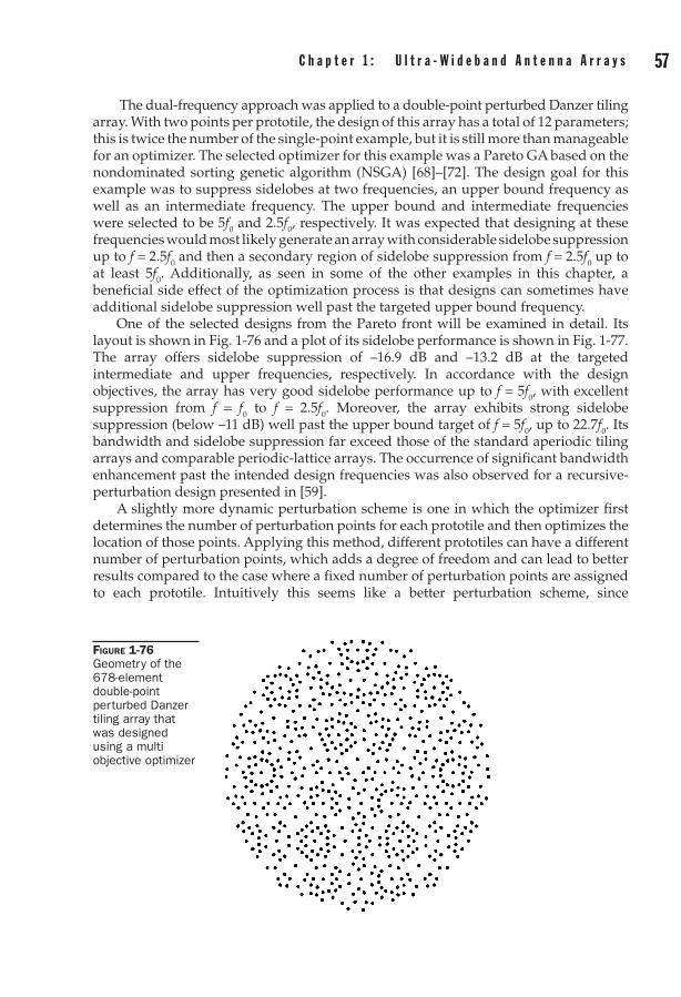
56 F r o n t i e r s i n a n t e n n a s : N e x t G e n e r a t i o n D e s i g n & e n g i n e e r i n g C h a p t e r 1 : U l t r a - W i d e b a n d a n t e n n a a r r a y s 57
The dual-frequency approach was applied to a double-point perturbed Danzer tiling array. With two points per prototile, the design of this array has a total of 12 parameters; this is twice the number of the single-point example, but it is still more than manageable for an optimizer. The selected optimizer for this example was a Pareto GA based on the nondominated sorting genetic algorithm (NSGA) [68]–[72]. The design goal for this example was to suppress sidelobes at two frequencies, an upper bound frequency as well as an intermediate frequency. The upper bound and intermediate frequencies were selected to be 5f0 and 2.5f0, respectively. It was expected that designing at these frequencies would most likely generate an array with considerable sidelobe suppression up to f = 2.5f0 and then a secondary region of sidelobe suppression from f = 2.5f0 up to at least 5f0. Additionally, as seen in some of the other examples in this chapter, a beneficial side effect of the optimization process is that designs can sometimes have additional sidelobe suppression well past the targeted upper bound frequency.
One of the selected designs from the Pareto front will be examined in detail. Its layout is shown in Fig. 1-76 and a plot of its sidelobe performance is shown in Fig. 1-77. The array offers sidelobe suppression of –16.9 dB and –13.2 dB at the targeted intermediate and upper frequencies, respectively. In accordance with the design objectives, the array has very good sidelobe performance up to f = 5f0, with excellent suppression from f = f0 to f = 2.5f0. Moreover, the array exhibits strong sidelobe suppression (below –11 dB) well past the upper bound target of f = 5f0, up to 22.7f0. Its bandwidth and sidelobe suppression far exceed those of the standard aperiodic tiling arrays and comparable periodic-lattice arrays. The occurrence of significant bandwidth enhancement past the intended design frequencies was also observed for a recursive-perturbation design presented in [59].
A slightly more dynamic perturbation scheme is one in which the optimizer first determines the number of perturbation points for each prototile and then optimizes the location of those points. Applying this method, different prototiles can have a different number of perturbation points, which adds a degree of freedom and can lead to better results compared to the case where a fixed number of perturbation points are assigned to each prototile. Intuitively this seems like a better perturbation scheme, since
Figure 1-76 Geometry of the 678-element double-point perturbed Danzer tiling array that was designed using a multi objective optimizer
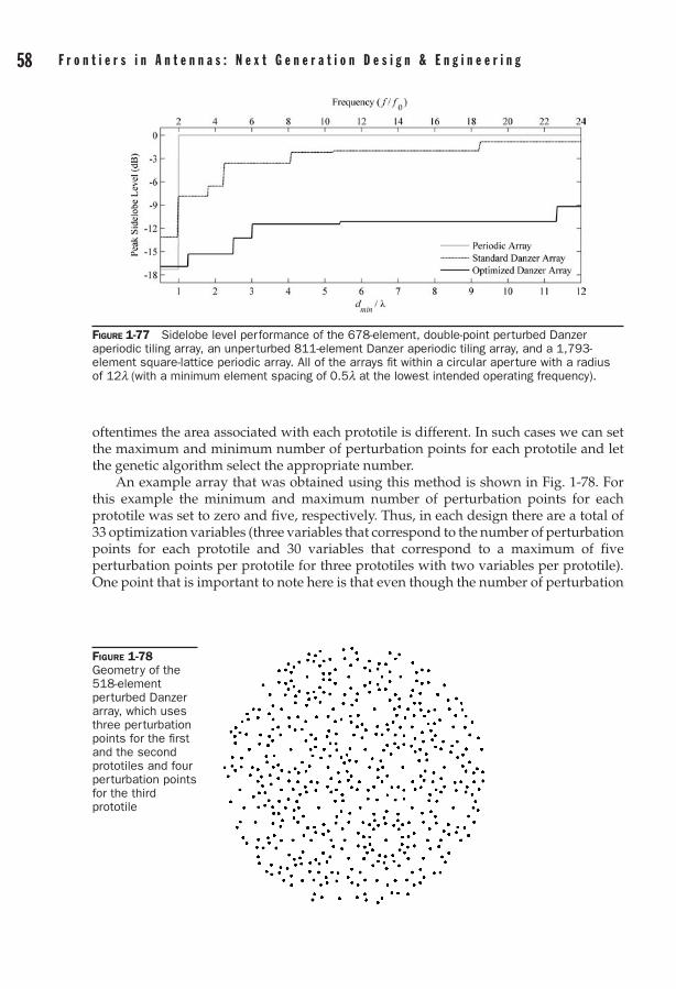
58 F r o n t i e r s i n a n t e n n a s : N e x t G e n e r a t i o n D e s i g n & e n g i n e e r i n g C h a p t e r 1 : U l t r a - W i d e b a n d a n t e n n a a r r a y s 59
oftentimes the area associated with each prototile is different. In such cases we can set the maximum and minimum number of perturbation points for each prototile and let the genetic algorithm select the appropriate number.
An example array that was obtained using this method is shown in Fig. 1-78. For this example the minimum and maximum number of perturbation points for each prototile was set to zero and five, respectively. Thus, in each design there are a total of 33 optimization variables (three variables that correspond to the number of perturbation points for each prototile and 30 variables that correspond to a maximum of five perturbation points per prototile for three prototiles with two variables per prototile). One point that is important to note here is that even though the number of perturbation
Figure 1-78 Geometry of the 518-element perturbed Danzer array, which uses three perturbation points for the first and the second prototiles and four perturbation points for the third prototile
Figure 1-77 Sidelobe level performance of the 678-element, double-point perturbed Danzer aperiodic tiling array, an unperturbed 811-element Danzer aperiodic tiling array, and a 1,793-element square-lattice periodic array. All of the arrays fit within a circular aperture with a radius of 12l (with a minimum element spacing of 0.5l at the lowest intended operating frequency).

58 F r o n t i e r s i n a n t e n n a s : N e x t G e n e r a t i o n D e s i g n & e n g i n e e r i n g C h a p t e r 1 : U l t r a - W i d e b a n d a n t e n n a a r r a y s 59
points for each prototile can be less than the maximum number allowed, in the process used here we have incorporated the maximum number of variables in each chromosome for the genetic algorithm. When the number of perturbation points is less than the maximum, the additional values are simply disregarded.
The goal of this design was to maximize sidelobe suppression at f = 30f0. The resulting array has 518 elements with three perturbation points for the first and second prototiles and four perturbation points for the third prototile. Some of the salient properties of this array are summarized in Table 1-12. A plot of its sidelobe suppression performance is shown in Fig. 1-79. A significant sidelobe suppression effect exits far beyond the targeted optimization frequency resulting in a very large operating bandwidth of 63:1.
1.4.4 Volumetric Array Based on a 3D Aperiodic TilingAn additional degree of complexity comes into play when designing 3D volumetric arrays for wideband performance. Mathematically it can be shown that, for planar arrays, the peak sidelobe level is a nondecreasing function of frequency. This concept is fairly straightforward to prove, and can be visually illustrated as in Fig. 1-32. Assuming that we have a planar array in xy-plane and the array factor has been calculated at a given frequency, then the array factor at any lower frequency can be extracted from this array factor. Let AF(q, j, f ) denote the array factor of a planar array evaluated at frequency f, and AF(q, j, f / m) be the array factor evaluated at frequency (f /m) for m > 1, then the following relationship holds between the two array factors:
AFfm
AFm
fθ φ θ φ, , sinsin
, ,
=
-1 (1-44)
Thus, for a planar array, if we meet a certain sidelobe level performance at a given frequency, the peak sidelobe level at all lower frequencies will be at least as good. However, the same cannot be said for a general volumetric array. Therefore, in order to design UWB 3D arrays, one must target different values of frequencies in the required
Figure 1-79 Sidelobe level performance of the 518-element multipoint optimized Danzer tiling array, a standard Danzer tiling array, and a standard square-lattice periodic array. The isotropic elements are uniformly excited and steered to broadside.

60 F r o n t i e r s i n a n t e n n a s : N e x t G e n e r a t i o n D e s i g n & e n g i n e e r i n g C h a p t e r 1 : U l t r a - W i d e b a n d a n t e n n a a r r a y s 61
bandwidth. For instance, assume an array is to be designed to have a peak sidelobe level less than r (dB) at N different frequencies. In such a case, the following cost function can be defined as
F f rnn
N
==
∑ ramp PSLL( ( ), )1
(1-45)
where
ramp( , )x ax a
x a x a= <
- ≥
0 (1-46)
and PSLL (fn) is the peak sidelobe level of the array evaluated at a frequency fn. The cost function can be minimized using the array perturbation methods described in Section 1.3.3, where the elements are perturbed inside the base tetrahedrons shown in Fig. 1-23 rather than the triangles in Fig. 1-20.
As an example, we consider designing an array with a bandwidth of 30f0, where f0 is the operating frequency corresponding to half-wavelength minimum spacing between the elements. Using 20 equally spaced frequency points and a -10 dB peak sidelobe level goal, the following cost function is realized:
F f f f f f fnn
= - ∈=
ramp PSLL( ( ), ) , , , [ , ]10 301 2 20 0 0K11
20N=
∑ (1-47)
From the definition of the ramp function, the cost function has a minimum of zero, which can be used as the stopping criteria for the optimization method. Using the variable-point optimization method introduced in Section 1.4.3 with the prototiles in Fig. 1-23, a design with 720 elements is created. The optimized prototiles A and K have no perturbation elements, however, prototiles B and C have three and five perturbation elements, respectively. The optimized geometry of the array is shown in Fig. 1-80 and the properties of the design are summarized in Table 1-13.
Figure 1-81 shows the sidelobe performance of the optimized array over a wide frequency range. It can be seen from the plot that the sidelobe behavior of volumetric arrays is more complicated than planar arrays in the sense that the peak sidelobe level
Figure 1-80 The 720-element, optimized, 3D aperiodic perturbed Danzer array. Outer hull of 3D array (a), the hull with the elements included (b), and the element layout only (c).
(a) (b) (c)

60 F r o n t i e r s i n a n t e n n a s : N e x t G e n e r a t i o n D e s i g n & e n g i n e e r i n g C h a p t e r 1 : U l t r a - W i d e b a n d a n t e n n a a r r a y s 61
at one frequency has no bearing on the peak sidelobe level at another frequency. While this property can make obtaining UWB volumetric arrays more cumbersome, for certain applications it might be desirable. For example, consider designing an array with low sidelobe levels over two frequency bands that are separated by a large bandwidth. Using linear or planar arrays would make this task very challenging and, depending on the size of the separation band, it might require a large number of antenna elements. However, using aperiodic volumetric arrays, this can be accomplished much more simply and with a much smaller number of antenna elements.
1.5 Full-Wave and Experimental Verification of UWB DesignsThe analysis in the preceding sections was based on the assumption that the arrays are comprised of isotropic radiators. This type of idealized analysis is useful for analyzing array factor patterns and for determining characteristics such as bandwidth, directivity, half-power beamwidth, etc. However, it lacks the ability to accurately predict and account for interactions among neighboring elements in an actual array environment. These interactions can impact a number of different aspects of an array, including driving-point impedances and radiation patterns.
Array Type NA NB NC NK
Peak SLL over Bandwidth Directivity
–3 dB Beamwidth davg dmax
720-Element 3D
Perturbed
Danzer Array
0 3 5 0 –10.28 dB 27.35 dB 2.04° 0.73l 3.96l
Table 1-13 Characteristics of the Optimized Perturbed Volumetric Danzer Aarray. NA, N
B, N
C, and
NK denote the number of perturbation points for each prototile shown in Fig. 1-23. The last four
columns correspond to operation at dmin
= 0.5l (f = f0).
Figure 1-81 Sidelobe level performance of the multipoint perturbed volumetric Danzer tiling array from Table 1-13. The periodic array possesses 0 dB peak sidelobe level at all frequencies (front and back beam in addition to any grating lobes) of operation due to symmetry of the array.

62 F r o n t i e r s i n a n t e n n a s : N e x t G e n e r a t i o n D e s i g n & e n g i n e e r i n g C h a p t e r 1 : U l t r a - W i d e b a n d a n t e n n a a r r a y s 63
One of the typical approaches for taking these interactions into account in a large linear or planar periodic array is to assume the array is of infinite extent, model an element of the array, and then use its characteristics to infer properties of the overall finite array. Various commercial software packages can readily handle this type of model. Alternatively, instead of using an infinite array model, an element at the center of the array could be modeled in the presence of a large number of neighboring elements to take into account mutual coupling. Its characteristics would then be used to infer the properties of the full array. The accuracy of both of these approaches can usually be improved by making corrections for elements near the edges of the array.
Extending these modeling approaches to aperiodic arrays is not straightforward due to the variety of element spacings that might make up their element distribution. Predicting and accounting for this in a linear aperiodic array might be feasible [81]–[88], however, it is significantly more difficult when factoring in the variety of element positions that might be present in a planar aperiodic array. There are different approaches available for handling this type of problem. For example, one approach involves modeling a moderately sized portion of an aperiodic array, and then inferring properties of the overall array based on the behavior of the subarray portion. Alternatively, the use of a simple radiator model might be sufficient to analyze the full array, while still garnering adequate information about how a particular lattice might be impacted by inter-element interactions.
The remainder of this chapter looks at using full-wave models to analyze several of the wideband aperiodic array distributions presented in Section 1.4. In addition, experimental data will be shown for two of the arrays. All of the examples in this section utilize a basic narrowband radiator in the full-wave model. This reduces the complexity of the model while still allowing the array to be analyzed over a range of frequencies. This can carried out by fixing the element spacing and scaling the dimensions of the element according to the operating frequency, or by fixing the dimensions of the element and scaling the spacing between elements to simulate a change in frequency. Either approach will provide insight into the coupling behavior of the aperiodic lattices under consideration. Both approaches will be implemented in this section.
1.5.1 Full-Wave Simulation of a Moderately Sized Optimized RPS ArrayThe 425-element, three-stage, ultra-wideband RPS array from Section 1.4 was selected for a more detailed full-wave analysis. The analysis was based on a method-of-moments formulation, which utilized a simple wire dipole as the radiator. The software utilized in the analysis was capable of accounting for the entire array in the model. At a very basic level, the full-wave model provides verification of the array factor formulation used in Section 1.4. Moreover, it can be used to investigate the effects of mutual coupling on the elements and the overall radiation pattern of the array. The full-wave model was analyzed at a set of frequencies across the bandwidth of the array to observe its wideband performance. At each frequency the length of the dipoles was scaled accordingly while the physical locations of the elements remained fixed, effectively emulating an UWB element.
As a somewhat arbitrary selection, a minimum operating frequency of 300 MHz was chosen corresponding to a wavelength of one meter. This gives the array a minimum element spacing of 0.5l, or 0.5 meters. This yielded a design with the fixed element locations shown in Fig. 1-82. Dipole elements are arranged in a parallel fashion as

62 F r o n t i e r s i n a n t e n n a s : N e x t G e n e r a t i o n D e s i g n & e n g i n e e r i n g C h a p t e r 1 : U l t r a - W i d e b a n d a n t e n n a a r r a y s 63
illustrated in Fig. 1-82, allowing direct comparison of the simulated radiation patterns [89] with the computed isotropic array factors in the plane normal to the dipoles. For the simulation at 300 MHz, dipole lengths of 48.3 cm were used with source impedances of 75Ω. In isolation, a single dipole has a VSWR of 1.14:1. In the array environment, the dipole sources experience the standing wave ratios shown in Fig. 1-83. At this relatively close element spacing, some of the dipoles possess a VSWR of greater than 2:1 due to mutual coupling. Despite the effects of mutual coupling, the radiation pattern of the array remains in fairly good agreement with the computed isotropic array factor as shown in Fig. 1-84.
Next, the array was simulated at a minimum element spacing of 2l, a region where grating lobes would appear in a periodic array. At the operating frequency of 1.2 GHz, a dipole length of 12.1 cm was selected, yielding an isolated VSWR of 1.24:1. Since the dipoles are all now at a greater electrical distance from each other, the mean VSWR of the elements improves as shown in Fig. 1-85. Again, there is good agreement with the simulated radiation pattern and the computed array factor in Fig. 1-86. Lastly, the array
Figure 1-82 Physical element locations for the 425-element array. Dipole lengths are not to scale. (From M. D. Gregory, and D. H. Werner, © IEEE 2010, [58].)
Figure 1-83 VSWR of the dipole antennas in the 425-element, UWB RPS array at an operating frequency of 300 MHz (d
min = 0.5l) (From M. D. Gregory, and D. H. Werner, © IEEE 2010, [58])
Figure 1-84 Comparison of the patterns from the full-wave analysis and an array factor formulation for the 425-element, UWB RPS array at an operating frequency of 300 MHz (d
min =
0.5l) (From M. D. Gregory, and D. H. Werner, © IEEE 2010, [58])
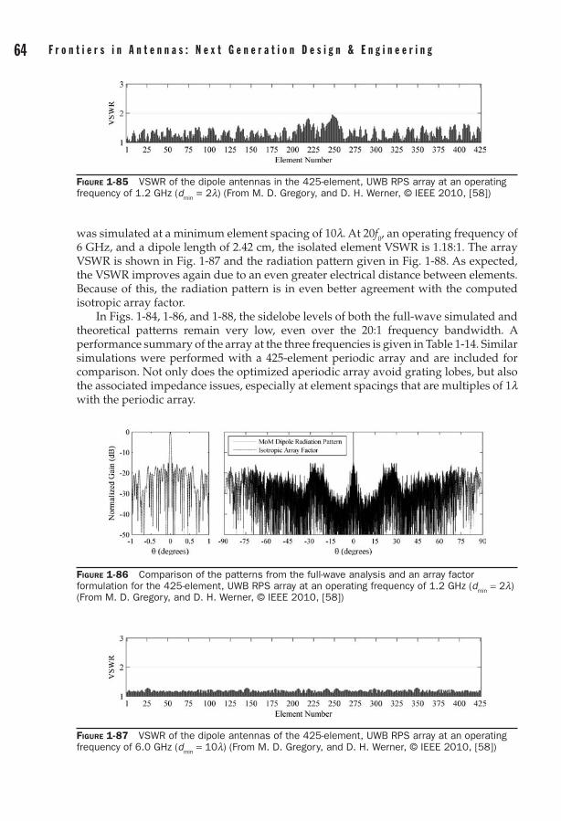
64 F r o n t i e r s i n a n t e n n a s : N e x t G e n e r a t i o n D e s i g n & e n g i n e e r i n g C h a p t e r 1 : U l t r a - W i d e b a n d a n t e n n a a r r a y s 65
was simulated at a minimum element spacing of 10l. At 20f0, an operating frequency of 6 GHz, and a dipole length of 2.42 cm, the isolated element VSWR is 1.18:1. The array VSWR is shown in Fig. 1-87 and the radiation pattern given in Fig. 1-88. As expected, the VSWR improves again due to an even greater electrical distance between elements. Because of this, the radiation pattern is in even better agreement with the computed isotropic array factor.
In Figs. 1-84, 1-86, and 1-88, the sidelobe levels of both the full-wave simulated and theoretical patterns remain very low, even over the 20:1 frequency bandwidth. A performance summary of the array at the three frequencies is given in Table 1-14. Similar simulations were performed with a 425-element periodic array and are included for comparison. Not only does the optimized aperiodic array avoid grating lobes, but also the associated impedance issues, especially at element spacings that are multiples of 1l with the periodic array.
Figure 1-85 VSWR of the dipole antennas in the 425-element, UWB RPS array at an operating frequency of 1.2 GHz (d
min = 2l) (From M. D. Gregory, and D. H. Werner, © IEEE 2010, [58])
Figure 1-86 Comparison of the patterns from the full-wave analysis and an array factor formulation for the 425-element, UWB RPS array at an operating frequency of 1.2 GHz (d
min = 2l)
(From M. D. Gregory, and D. H. Werner, © IEEE 2010, [58])
Figure 1-87 VSWR of the dipole antennas of the 425-element, UWB RPS array at an operating frequency of 6.0 GHz (d
min = 10l) (From M. D. Gregory, and D. H. Werner, © IEEE 2010, [58])
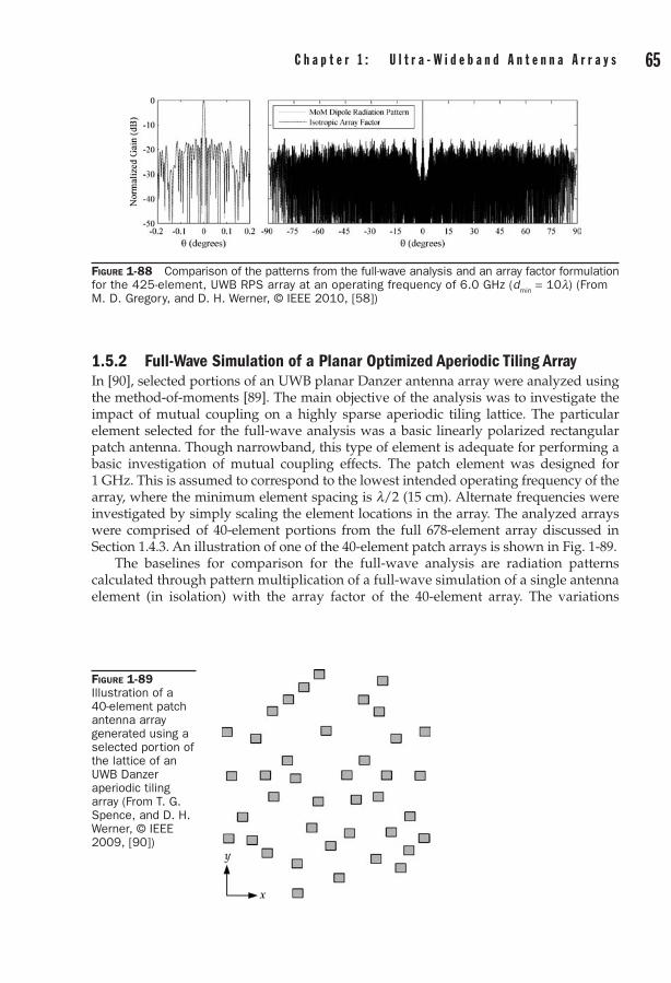
64 F r o n t i e r s i n a n t e n n a s : N e x t G e n e r a t i o n D e s i g n & e n g i n e e r i n g C h a p t e r 1 : U l t r a - W i d e b a n d a n t e n n a a r r a y s 65
1.5.2 Full-Wave Simulation of a Planar Optimized Aperiodic Tiling ArrayIn [90], selected portions of an UWB planar Danzer antenna array were analyzed using the method-of-moments [89]. The main objective of the analysis was to investigate the impact of mutual coupling on a highly sparse aperiodic tiling lattice. The particular element selected for the full-wave analysis was a basic linearly polarized rectangular patch antenna. Though narrowband, this type of element is adequate for performing a basic investigation of mutual coupling effects. The patch element was designed for 1 GHz. This is assumed to correspond to the lowest intended operating frequency of the array, where the minimum element spacing is l/2 (15 cm). Alternate frequencies were investigated by simply scaling the element locations in the array. The analyzed arrays were comprised of 40-element portions from the full 678-element array discussed in Section 1.4.3. An illustration of one of the 40-element patch arrays is shown in Fig. 1-89.
The baselines for comparison for the full-wave analysis are radiation patterns calculated through pattern multiplication of a full-wave simulation of a single antenna element (in isolation) with the array factor of the 40-element array. The variations
Figure 1-88 Comparison of the patterns from the full-wave analysis and an array factor formulation for the 425-element, UWB RPS array at an operating frequency of 6.0 GHz (d
min = 10l) (From
M. D. Gregory, and D. H. Werner, © IEEE 2010, [58])
Figure 1-89 Illustration of a 40-element patch antenna array generated using a selected portion of the lattice of an UWB Danzer aperiodic tiling array (From T. G. Spence, and D. H. Werner, © IEEE 2009, [90])
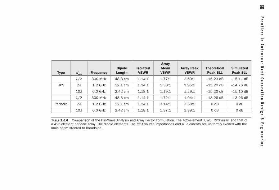
66
Frontiers in a
ntennas: N
ext Generatio
n Design &
engineerin
g
Chapter 1:
Ultra-W
ideband antenna a
rrays 67
Type dmin FrequencyDipole Length
Isolated VSWR
Array Mean VSWR
Array Peak VSWR
Theoretical Peak SLL
Simulated Peak SLL
l/2 300 MHz 48.3 cm 1.14:1 1.77:1 2.50:1 –15.23 dB –15.11 dB
RPS 2l 1.2 GHz 12.1 cm 1.24:1 1.33:1 1.95:1 –15.20 dB –14.76 dB
10l 6.0 GHz 2.42 cm 1.18:1 1.19:1 1.29:1 –15.20 dB –15.10 dB
l/2 300 MHz 48.3 cm 1.14:1 1.72:1 1.94:1 –13.26 dB –13.26 dB
Periodic 2l 1.2 GHz 12.1 cm 1.24:1 3.14:1 3.33:1 0 dB 0 dB
10l 6.0 GHz 2.42 cm 1.18:1 1.37:1 1.39:1 0 dB 0 dB
Table 1-14 Comparison of the Full-Wave Analysis and Array Factor Formulation. The 425-element, UWB, RPS array, and that of a 425-element periodic array. The dipole elements use 75Ω source impedances and all elements are uniformly excited with the main beam steered to broadside.

66 F r o n t i e r s i n a n t e n n a s : N e x t G e n e r a t i o n D e s i g n & e n g i n e e r i n g C h a p t e r 1 : U l t r a - W i d e b a n d a n t e n n a a r r a y s 67
between the full-wave analysis data and this “idealized” case will illustrate the impact that the array environment has on the radiation characteristics of the microstrip patch array. In addition to pattern comparisons, the driving-point impedance of each patch element was calculated for the full-wave model and compared with that of the single-patch in isolation.
E- and H-plane radiation pattern cuts of a patch array (Fig. 1-89) with a broadside-directed main beam and a steered main beam are shown in Figs. 1-90 and 1-91, respectively. In each case excellent agreement was observed between the full-wave analysis and pattern multiplication data. Even while steering along the direction of maximum coupling for the patch elements (along the E-plane of the patch) there was minimal deviation between the two pattern models. This agreement gives an indication that the radiation characteristics of the patch antennas are relatively unaffected by the presence of neighboring elements in this sparse array environment. While the radiation characteristics are minimally affected, coupling among radiating elements is seen to
0
–10
–20
–30
–40–90 –60 –30 0 30 60 90
Theta (degrees)
Nor
mal
ized
Rad
iati
onPa
tter
n (d
B)
Full-Wave AnalysisPattern Multiplication
(a)
0
–10
–20
–30
–40–90 –60 –30 0 30 60 90
Theta (degrees)(b)
Nor
mal
ized
Rad
iati
onPa
tter
n (d
B)
Full-Wave AnalysisPattern Multiplication
Figure 1-90 Radiation pattern cuts along (a) j = 0° (H-plane of the microstrip patch elements) and (b) j = 90° (E-plane of the microstrip patch elements) for a 40-element portion of the 678-element Danzer tiling array with d
min = l/2 at f = 1 GHz and its main beam directed to
broadside.
0
–10
–20
–30
–40–90 –60 –30 0 30 60 90
Theta (degrees)(a)
Nor
mal
ized
Rad
iati
onPa
tter
n (d
B)
Full-Wave AnalysisPattern Multiplication
0
–10
–20
–30
–40–90 –60 –30 0 30 60 90
Theta (degrees)(b)
Nor
mal
ized
Rad
iati
onPa
tter
n (d
B)
Full-Wave AnalysisPattern Multiplication
Figure 1-91 Radiation pattern cuts along the beam steering direction with the main beam directed to (a) j = 0°, q = 30° and (b) j = 90°, q = 30° for a 40-element portion of the 678-element Danzer tiling array with d
min = l/2 at f = 1 GHz.

68 F r o n t i e r s i n a n t e n n a s : N e x t G e n e r a t i o n D e s i g n & e n g i n e e r i n g C h a p t e r 1 : U l t r a - W i d e b a n d a n t e n n a a r r a y s 69
impact the driving-point impedances during beam steering. For instance, in some cases the real part of the driving-point impedance drops to nearly zero ohms for array elements while steering 30° off broadside. However, the effects on the driving-point impedances were observed to lessen with only a slight increase in the minimum element spacing of the array [90]. Restricting operations to larger spacings, such as 0.75l, might be a limiting factor for conventional periodic arrays but it has considerably less of an impact on perturbed aperiodic tiling arrays due to their relatively wide bandwidths.
1.5.3 Experimental Verification of Two Linear Polyfractal ArraysMeasured data was taken for the two 32-element polyfractal arrays (designs A and B) discussed in Section 1.4.1. Following the approaches of the previous two sections, the arrays were fabricated based on narrowband radiators, specifically microstrip patch antennas. The aim of the effort was to build two separate arrays for each design: one array built for operation with a minimum element spacing of 0.5l (f = f0) and the other for operation at a spacing of 2l (f = 4f0). The use of the narrowband elements and two separate arrays (for each polyfractal design) simplified the design and construction of the radiating elements and feed structure. Due to limitations of the available test facilities and standard printed circuit board sizes, the design frequencies were selected to be 5 GHz and 20 GHz, and the array fabrication was divided into four subarray boards for each array. Each subarray board had its own corporate feed network leading down to a single SMA connector. Each subarray was tested individually and the resulting patterns were combined to form the total 32-element array. The subarray boards were designed based on 0.254 mm thick Rogers RT/Duroid 5880. The design and layout of the boards was carried out using a method-of-moments software package [91].
The board layouts for the two 32-element polyfractal arrays are shown in Fig. 1-92. The features shown form the top copper layer of the fabricated PCB, while a solid copper bottom layer forms the ground plane. H-plane cuts of the radiation pattern for the four subarrays of array A are shown in Fig. 1-93 for dmin = 0.5l and in Fig. 1-94 for dmin = 2l. Pattern multiplication was then used to generate the pattern of the full array at each frequency. The resulting patterns for array A and array B are shown in Fig. 1-95 through Fig. 1-98.
Figure 1-92 From top to bottom, the subarray layouts of polyfractal array A at 5 GHz, array A at 20 GHz, array B at 5 GHz, and array B at 20 GHz (From M. D. Gregory, et al., © IEEE 2010, [78])

68 F r o n t i e r s i n a n t e n n a s : N e x t G e n e r a t i o n D e s i g n & e n g i n e e r i n g C h a p t e r 1 : U l t r a - W i d e b a n d a n t e n n a a r r a y s 69
Figure 1-93 Normalized radiation patterns at 5 GHz (dmin
= 0.5l) for subarrays 1 (a) through 4 (d) of the 32-element polyfractal array A
(a) (b)
(c) (d)
Figure 1-94 Normalized radiation patterns at 20 GHz (dmin
= 2.0l) for subarrays 1 (a) through 4 (d) of the 32-element polyfractal array A
(a) (b)
(c) (d)

70 F r o n t i e r s i n a n t e n n a s : N e x t G e n e r a t i o n D e s i g n & e n g i n e e r i n g C h a p t e r 1 : U l t r a - W i d e b a n d a n t e n n a a r r a y s 71
Figure 1-95 Total radiation patterns for the polyfractal array A at 5 GHz (dmin
= 0.5l)
Figure 1-96 Total radiation patterns for the polyfractal array A at 20 GHz (dmin
= 2l)
Figure 1-97 Total radiation patterns for the polyfractal array B at 5 GHz (dmin
= 0.5l)

70 F r o n t i e r s i n a n t e n n a s : N e x t G e n e r a t i o n D e s i g n & e n g i n e e r i n g C h a p t e r 1 : U l t r a - W i d e b a n d a n t e n n a a r r a y s 71
Excellent agreement is noted at 5 GHz between the full-wave analysis and the measured data for the full array. At this frequency there is negligible difference between the peak sidelobe level of the modeled and measured data for array B, and the difference is 1 dB for array A. At 20 GHz there is also good agreement. The difference between modeled and measured results for both arrays is approximately 1.3 dB. The performance of the arrays is summarized in Table 1-15. It is interesting to point out the need to accurately model the arrays as individual subarrays in order to match the test configuration. For the “Simulated Full Array,” the feed branch leading to the four subarrays was incorporated into the full-wave model. As can be seen in Figs. 1-95 through 1-98, this long length of transmission line has a significant impact on the radiation pattern of the array. Overall there was very good agreement between the theory and measurements for the 32-element polyfractal arrays. Images of the fabricated subarray panels are shown in Fig. 1-99, where the relatively large microstrip transmission line sections can easily be observed.
Figure 1-98 Total radiation patterns for the polyfractal array B at 20 GHz (dmin
= 2l)
Table 1-15 Performance of the Two Example Polyfractal Designs at Both Operating Frequencies
Array dmin Frequency
Measured Subarray Peak SLL
Simulated Subarray Peak SLL
Simulated Full Array Peak SLL
A 0.5l 5.0 GHz –16.3 dB –17.4 dB –14.3 dB
A 2.0l 20 GHz –5.39 dB –6.77 dB –7.11 dB
B 0.5l 5.0 GHz –14.75 dB –14.79 dB –14.34 dB
B 2.0l 20 GHz –3.58 dB –4.88 dB –7.24 dB

72 F r o n t i e r s i n a n t e n n a s : N e x t G e n e r a t i o n D e s i g n & e n g i n e e r i n g C h a p t e r 1 : U l t r a - W i d e b a n d a n t e n n a a r r a y s 73
ReferencesM. I. Skolnik, [1] Introduction to Radar Systems, 3rd ed. Boston: McGraw Hill, 2001.H. A. Wheeler, “The grating lobe series for the Impedance variation in a planar phased-array [2] antenna,” IEEE Transactions on Antennas and Propagation, vol. 14, no. 6, pp. 707–714, November 1966.C. A. Balanis, [3] Antenna Theory: Analysis and Design, 3rd ed. New Jersey: Wiley, 2005.J. J. Lee, “Ultra-wideband arrays,” in J. L. Volakis[4] , Antenna Engineering Handbook, 4th Edition, Chapter 24, 2007. H. A. Wheeler, “The radiation resistance of an antenna in an infinite array or waveguide,” [5] Proc. IRE, vol. 36, pp. 478–488, April 1948.R. C. Hansen, “Linear connected arrays,” [6] IEEE Antennas and Wireless Propagation Letters, vol. 3, pp. 154–156, 2004.A. Q. Boryssenkko, and D. H. Schaubert, “Physical aspects of mutual coupling in finite broadband [7] tapered slot (Vivaldi) arrays,” 5th International Conference on Antenna Theory and Techniques, Kiev, Ukraine, May 24–27, 2005.B. D. Steinberg, “The peak sidelobe of the phased array having randomly located elements,” [8] IEEE Transactions on Antennas and Propagation, vol. 20, no. 2, pp. 129–136, March 1972.B. D. Steinberg, “comparison between the peak sidelobe of the random array and algorithmically [9] designed aperiodic arrays,” IEEE Transactions on Antennas and Propagation, vol. 21, no. 3, pp. 366–370, May 1973.Y. T. Lo, “Sidelobe level in nonuniformly spaced arrays,” [10] IEEE Transactions on Antennas and Propagation, vol. 11, no. 4, pp. 511–512, July 1963.Y. T. Lo, “A probabilistic approach to the design of large antenna arrays,” [11] IEEE Transactions on Antennas and Propagation, vol. 11, no. 1, pp. 95–96, January 1963.Y. T. Lo, “A Mathematical theory of antenna arrays with randomly spaced elements,” [12] IEEE Transactions on Antennas and Propagation, vol. 12, no. 3, pp. 257–268, May 1964.D. L. Jaggard, and A. D. Jaggard, “Cantor ring arrays,” [13] Microwave and Optical Technology Letters, vol. 19, no. 2, pp. 121–125, October 1998.Y. Kim, and D. L. Jaggard, “The fractal random array,” [14] Proceedings of the IEEE, vol. 74, no. 9, pp.1278–1280, September 1986.D. H. Werner, and R. Mittra, eds., [15] Frontiers in Electromagnetics. Piscataway, NJ: Wiley-IEEE Press, 2000.E. D. Sharp, “A triangular arrangement of planar-array elements that reduces the number needed,” [16] IRE Transactions on Antennas and Propagation, vol. 9, no. 2 pp. 126–129, 1961.A. Ishimaru, and Y-S. Chen, “Thinning and broadbanding antenna arrays by unequal spacings,” [17] IEEE Transactions on Antennas and Propagation, vol. 13, no. 1, pp. 34–42, January 1965.M. B. Donvito, and S. A. Kassam, “Characterization of the random array peak sidelobe level,” [18] IEEE Transactions on Antennas and Propagation, vol. 27, no. 3, pp. 379–385, May 1979.
Figure 1-99 Photos of the example polyfractal design A subarrays for (a) 5 GHz and (b) 20 GHz (From M. D. Gregory, et al., © IEEE 2010, [78])
(a) (b)

72 F r o n t i e r s i n a n t e n n a s : N e x t G e n e r a t i o n D e s i g n & e n g i n e e r i n g C h a p t e r 1 : U l t r a - W i d e b a n d a n t e n n a a r r a y s 73
V. D. Agrawal, and Y. T. Lo, “Distribution of sidelobe level in random arrays,” [19] Proceedings of the IEEE, vol. 57, no. 10, pp. 1764–1765, October 1969.Y. T. Lo, and R. J. Simcoe, “An experiment on antenna arrays with randomly spaced elements,” [20] IEEE Transactions on Antennas and Propagation, vol. 15, no. 2, pp. 231–235, March 1967.D. D. King, R. F. Packard, and R. K. Thomas, “Unequally-spaced, broad-band antenna arrays,” [21] IRE Transactions on Antennas and Propagation, vol. 8, no. 4, pp. 380–384, July 1960.R. Das, “Broadbanding of concentric planar ring arrays by space tapering,” [22] Radio and Electronic Engineer, vol. 33, no. 4, pp. 211–222, April 1967.Y. T. Lo, and S. W. Lee, “A study of space-tapered arrays,” [23] IEEE Transactions on Antennas and Propagation, vol. 14, no. 1, pp. 22–30, January 1966.J. Galejs, “Minimization of sidelobes in space tapered linear arrays,” [24] IEEE Transactions on Antennas and Propagation, vol. 12, no. 4, pp. 497–498, July 1964.R. Willey, “Space tapering of linear and planar arrays,” [25] IRE Transactions on Antennas and Propagation, vol. 10, no. 4, pp. 369–377, July 1962.M. G. Bray, D. H. Werner, D. W. Boeringer, and D. W. Machuga, “Optimization of thinned aperi-[26] odic linear phased arrays using genetic algorithms to reduce grating lobes during scanning,” IEEE Transactions on Antennas and Propagation, vol. 50, no. 12, pp. 1732–1742, December 2002.B. B. Mandelbrot, [27] The Fractal Geometry of Nature. New York: W. H. Freeman, 1983.H. O. Peitgen, H. Jurgens, and D. Saupe, [28] Chaos and Fractals: New Frontiers of Science. New York: Springer-Verlag, Inc., 1992.M. F. Barnsley, [29] Fractals Everywhere. 2nd Ed. New York: Academic Press Professional, 1993.D. H. Werner, R. L. Haupt, and P. L. Werner, “Fractal antenna engineering: The theory and design of [30] fractal antenna arrays,” IEEE Antennas and Propagation Magazine, vol. 41, no. 5, pp. 37–59, October 1999.D. H. Werner, and P. L. Werner, “On the synthesis of fractal radiation patterns,” [31] Radio Science, vol. 30, no. 1, pp. 29–45, 1995.X. Liang, W. Zhensen, and W. Wenbing, “Synthesis of fractal radiation patterns from concentric ring [32] arrays,” Electronics Letters, vol. 32, no. 21, pp. 1940–1941, October 1996.D. H. Werner, and P. L. Werner, “Frequency-independent features of self-similar fractal antennas,” [33] Radio Science, vol. 31, no. 6, pp. 1331–1343, 1996.C. Puente-Baliarda, and R. Pous, “Fractal design of multiband and low side-lobe arrays,” [34] IEEE Transactions on Antennas and Propagation, vol. 44, no. 5, pp. 730–39, May 1996.D. H. Werner, and S. Ganguly, “An overview of fractal antenna engineering research,” [35] IEEE Antennas and Propagation Magazine, vol. 45, no. 1, pp. 38–57, February 2003.D. H. Werner, M. A. Gingrich, and P. L. Werner, “A self-similar fractal radiation pattern synthesis [36] technique for reconfigurable multiband arrays,” IEEE Transactions on Antennas and Propagation, vol. 51, no. 7, pp.1486–1498, July 2003.V. F. Kravchenko, and V. M. Masyuk, “New method of synthesis of multiband fractal antenna arrays [37] based on a family of atomic functions,” Doklady Physics, vol. 49, no. 8, pp. 456–461, August 2004.M. Senechal[38] , Quasicrystals and Geometry. Cambridge, U.K.: Cambridge Univ. Press, 1995.B. Grünbaum, and G. C. Shephard, [39] Tilings and Patterns. New York: Freeman, 1990.
[40] D. H. Werner, W. Kuhirun, and P. L. Werner, “Fractile arrays: A new class of tiled arrays with fractal boundaries,” IEEE Transactions on Antennas and Propagation, vol. 52, no. 8, pp. 2008–2018, August 2004.
[41] J. N. Bogard, D. H. Werner, and P. L. Werner, “Comparison of the Peano-Gosper fractile array and the regular hexagonal array,” Microwave and Optical Technology Letters, vol. 43, no. 6, pp. 524–526, December 2004.
[42] D. H. Werner. W. Kuhirun, and P. L. Werner, “The Peano-Gosper fractal array,” IEEE Transactions on Antennas and Propagation, Vol. 51, No. 8, pp. 2063-2072, Aug. 2003.
[43] T. G. Spence, D. H. Werner, and J. N. Carvajal, “Modular broad band phased-arrays based on a nonuniform distribution of elements along the Peano-Gosper space-filling curve,” IEEE Transactions on Antennas and Propagation, Vol. 58, No. 2, pp. 600-604, Feb. 2010.
[44] D. H. Werner, J. S. Petko, and T. G. Spence, “Fractal antennas,” Chapter 33, The Antenna Engineering Handbook, 4th ed., John L. Volakis, editor, McGraw-Hill, 2007.
[45] T. G. Spence and D. H. Werner, “Generalized space-filling Gosper curves and their application to the design of wideband modular planar array antennas,” IEEE Transactions on Antennas and Propagation, in press.
[46] R. Penrose, “The role of aesthetics in pure and applied mathematical research,” Bulletin of the Institute of Mathematics and its Applications, vol. 10, pp. 266–274, 1974.
[47] N. G. de Bruijn, “Updown generation of penrose patterns,” Indagationes Mathem., vol. 1, no. 2, pp. 201–218, June 1990.

74 F r o n t i e r s i n a n t e n n a s : N e x t G e n e r a t i o n D e s i g n & e n g i n e e r i n g C h a p t e r 1 : U l t r a - W i d e b a n d a n t e n n a a r r a y s 75
[48] C. Goodman-Strauss, “matching rules and substitution tilings,” Ann. Math., vol. 147, pp. 181–223, 1998.
[49] K.-P. Nischke, and L. Danzer, “A construction of inflation rules based on n-fold symmetry,” Discrete Comput. Geometry, vol. 15, no. 2, pp. 221–236, February 1996.
[50] C. Radin, “The pinwheel tilings of the plane,” Annals of Mathematics, vol. 139, no. 3, pp. 661–701, May 1994.
[51] L. Danzer, “Three-dimensional analogs of the planar Penrose tilings and quasicrystals,” Discrete Mathematics, vol. 76, no. 1, pp. 1–7, 1989.
[52] L. Danzer, “Quasiperiodicity: Local and global aspects,” Lecture Notes in Physics, vol. 382, pp. 561–572, 1991.
[53] P. Kramer, and M. Andrle, “Inflation and wavelets for the icosahedral danzer tiling,” Journal of Physics A: Mathematical and General, vol. 37, pp. 3443–3457, 2004.
[54] F. Namin and D. H. Werner, “Design of Volumetric Antenna Arrays Based on Three-Dimensional Aperiodic Tilings,” IEEE International Symposium on Antennas and Propagation, Toronto, ON, July 2010.
[55] J. S. Petko, and D. H. Werner, “The evolution of optimal linear polyfractal arrays using genetic algorithms,” IEEE Transactions on Antennas and Propagation, vol. 53, no. 11, pp. 3604–3615, November 2005.
[56] J. S. Petko, and D. H. Werner, “An autopolyploidy-based genetic algorithm for enhanced evolution of linear polyfractal arrays,” IEEE Transactions on Antennas and Propagation, vol. 55, no. 3, pp. 583–593, March 2007.
[57] J. S. Petko, and D. H. Werner, “The pareto optimization of ultrawideband polyfractal arrays,” IEEE Transactions on Antennas and Propagation, vol. 56, no. 1, pp. 97–107, January 2008.
[58] M. D. Gregory, and D. H. Werner, “Ultra-wideband aperiodic antenna arrays based on optimized raised power series representations,” IEEE Transactions on Antennas and Propagation, vol. 58, no. 3, pp. 756–764, March 2010.
[59] T. G. Spence, and D. H. Werner, “Design of broadband planar arrays based on the optimization of aperiodic tilings,” IEEE Transactions on Antennas and Propagation, vol. 56, no. 1, pp. 76–86, January 2008.
[60] D. E. Goldberg, Genetic Algorithms in Search, Optimization & Machine Learning. Reading, MA: Addison-Wiley Publishing Company, Inc., 1989.
[61] R. L. Haupt, and S. E. Haupt, Practical Genetic Algorithms. New York: John Wiley & Sons, Inc., 1998.
[62] Y. Rahmat-Samii, and E. Michielssen, Editors, Electromagnetic Optimization by Genetic Algorithms. New York: John Wiley & Sons, Inc., 1999.
[63] R. L. Haupt, and D. H. Werner, Genetic Algorithms in Electromagnetics, John Wiley & Sons, Inc., Hoboken, NJ, 2007.
[64] J. Kennedy, and R. Eberhart, “Particle swarm optimization,” Proceedings of the Ninth International Conference on Neural Networks, vol. 4, pp. 1942–1948, November 1995.
[65] R. Eberhart, and J. Kennedy, “A new optimizer using particle swarm theory,” IEEE Proceedings of the Sixth International Symposium on Micro Machine and Human Science, pp. 39–43, October 1995.
[66] J. Robinson, and Y. Rahmat-Samii, “Particle swarm optimization in electromagnetics,” IEEE Transactions on Antennas and Propagation, vol. 52, no. 2, pp. 397–407, February 2004.
[67] D. W. Boeringer, and D. H. Werner, “Particle swarm optimization versus genetic algorithms for phased array synthesis,” IEEE Transactions on Antennas and Propagation, vol. 52, no. 3, pp. 771–779, March 2004.
[68] J. Horn, N. Nafpliotis, and D. E. Goldberg, “A niched Pareto genetic algorithm for multiobjective optimization,” in Proc. 1st IEEE Conference Evolutionary Computation, Piscataway, NJ, June 1994, vol. 1, pp. 82–87, IEEE World Congress on Computational Intelligence.
[69] N. Srinivas, and K. Deb, “Multiobjective optimization using nondominated sorting in genetic algorithms,” Evol. Comput., vol. 2, no. 3, pp. 221–248, Fall 1994.
[70] C. Fonseca, and P. Fleming, “An overview of evolutionary algorithms in multiobjective optimiza-tion,” Evol. Comput., vol. 3, no. 1, pp. 1–16, Spring 1995.
[71] E. Zitzler, and L. Thiele, “An evolutionary algorithm for multiobjective optimization: The strength Pareto approach,” Swiss Federal Institute Technol., Zurich, Switzerland, May 1998, TIK-Report.
[72] E. Zitzler, and L. Thiele, “Multiobjective evolutionary algorithms: A comparative case study and the strength Pareto approach,” IEEE Trans. Evolutionary Computation, vol. 3, no. 4, pp. 257–271, November 1999.
[73] S. Ohno, Evolution by Gene Duplication. Heidelberg, Germany: Springer-Verlag, 1970.[74] W. H. Li, Molecular Evolution. Sunderland, MA: Sinauer, 1999.

74 F r o n t i e r s i n a n t e n n a s : N e x t G e n e r a t i o n D e s i g n & e n g i n e e r i n g C h a p t e r 1 : U l t r a - W i d e b a n d a n t e n n a a r r a y s 75
[75] R. Frankham, D. Ballou, and D. A. Briscoe, Introduction to Conservation Genetics. New York: Cambridge Univ. Press, 2002.
[76] T. A. Brown, Genomes, 2nd ed. New York: Wiley, 2002.[77] V. Pierro, V. Galdi, G. Castaldi, I. M. Pinto, and L. B. Felsen, “Radiation properties of planar
antenna arrays based on certain categories of aperiodic tilings,” IEEE Transactions on Antennas and Propagation, vol. 53, no. 2, pp. 635–644, February 2005.
[78] M. D. Gregory, J. S. Petko, T. G. Spence, and D. H. Werner, “Nature-Inspired Design Techniques for Ultra-Wideband Aperiodic Antenna Arrays,” IEEE Antennas and Propagation Magazine, Vol. 52, No. 3, pp. 28-45, June 2010.
[79] M. D. Gregory, J. S. Petko, and D. H. Werner, “Design validation of prototype ultra-wideband linear polyfractal antenna arrays,” IEEE International Symposium on Antennas and Propagation, San Diego, CA, July 2008.
[80] J. S. Petko, and D. H. Werner, “Interleaved ultrawideband antenna arrays based on optimized poly-fractal tree structures,” IEEE Transactions on Antennas and Propagation, vol. 57, no. 9, pp. 2622–2632, July 2009.
[81] R. P. Jedlicka, M. T. Poe, and K. R. Carver, “Measured mutual coupling between microstrip anten-nas,” IEEE Transactions on Antennas and Propagation, vol. 29, no. 1, pp. 147–149, January 1981.
[82] A. H. Mohammadian, N. M. Martin, and D. W. Griffin, “A theoretical and experimental study of mutual coupling in microstrip antenna arrays,” IEEE Transactions on Antennas and Propagation, vol. 37, no. 10, pp. 1217–1223, October 1989.
[83] E. Penard, and J. P. Daniel, “Mutual coupling between microstrip antennas,” IEE Electronics Letters, vol. 18, no. 14, pp. 605–607, July 1982.
[84] E. H. Van Lil, and A. R. Van de Capelle, “Transmission line model for mutual coupling between microstrip antennas,” IEEE Transactions on Antennas and Propagation, vol. 32, no. 8, pp. 816–821, August 1984.
[85] P. B. Katehi, “A generalized method for the evaluation of mutual coupling in microstrip arrays,” IEEE Transactions on Antennas and Propagation, vol. 35, no. 2, pp. 125–133, February 1987.
[86] C. M. Krowne, “Dielectric and width effect on H-plane and E-plane coupling between rectangular microstrip antennas,” IEEE Transactions on Antennas and Propagation, vol. 31, no. 1, pp. 39–47, January 1983.
[87] H. Steyskal, and J. S. Herd, “Mutual coupling compensation in small array antennas,” IEEE Transactions on Antennas and Propagation, vol. 38, no. 12, pp. 1971–1975, December 1990.
[88] M. A. Khayat, J. T. Williams, D. R. Jackson, and S. A. Long, “Mutual coupling between reduced surface-wave microstrip antennas,” IEEE Transactions on Antennas and Propagation, vol. 48, no. 10, pp. 1581–1593, October 2000.
[89] FEKO. EM Software and Systems—S.A. [Online]. Version 5.4. Available: www.emssusa.com.[90] T. G. Spence, and D. H. Werner, “Full-wave mutual coupling analysis of wideband arrays based on
aperiodic tiling,” International Symposium on Antennas and Propagation, Charleston, SC, June 2009.[91] Ansoft Designer. Ansys, Inc. [online]. Version 2.2. Available: www.ansoft.com.

This page intentionally left blank

Chapter 2Smart antennas
Jeffrey D. Connor
2.1 IntroductionSmart antenna systems provide spatial separation between multiple emitters, reduce interference through cancellation, and increase resistance to multipath interference. Smart antenna systems are an important component of
Cellular Telephone Systems •
Satellite Communications•
Wireless LANs •
Radar•
Remote Sensing•
Direction Finding Systems•
Radio Astronomy•
The development of smart antenna systems was a natural progression of the early research into phased array techniques, which by the early 1950s was well understood. Early work into sensor array technology as well as mechanical and electronic scanning array technology was motivated by radar and direction finding systems. This work ultimately lead to adaptive arrays capable of responding to changes in the environment. Adaptive processing is the fundamental principle of a smart antenna system. The first “adaptive array” was the retrodirective array developed by Van Atta, which automati-cally reflected an incoming signal back to the source without a priori knowledge of its location. In 1959, Howells developed the sidelobe canceller as a countermeasure for radar jammers. The sidelobe canceller consists of an array composed of an omnidirectional antenna, and directive antenna. Desired signals are received by the mainlobe of the direc-tional antenna whereas interferers such as jammers are assumed to enter the sidelobes. The gain of the omnidirectional antenna is the same as the peak sidelobe of the direc-tional antenna. The weighted signal of the directional antenna is subtracted from the omnidirectional antenna effectively cancelling the interferer. Subsequently, Appelbaum developed the theory to control Howell’s adaptive array. Independent of this work, Wid-row developed a similar technique using the least mean square algorithm to adapt
77

78 F r o n t i e r s i n a n t e n n a s : N e x t G e n e r a t i o n D e s i g n & e n g i n e e r i n g C h a p t e r 2 : S m a r t a n t e n n a s 79
the array output to minimize mean square error with a desired signal. Subsequently, research has been conducted over the years to improve the convergence speed of the adaptive array as well as removing the need for a priori knowledge of the desired sig-nal. Alternative to adaptive systems, direction-of-arrival estimation has also been an important component of smart antenna systems. Radio direction finding techniques are as old as radio itself with the first work performed by Heinrich Hertz in 1888. These techniques played an important role in early radar systems where it was necessary to direct the array’s beampattern at a given direction. Modern systems have replaced con-ventional analog smart antenna systems with digital hardware and software capable of processing immense amounts of data in near real-time.
Smart antenna research has been active for over fifty years. Over this time, practical use of smart antennas has been limited mainly due to the cost and complexity of sys-tems both physically and computationally. Modern computing systems have alleviated many of these concerns, and as a result smart antennas and adaptive processing have become a fundamental component of wireless communications in the twenty-first cen-tury. The resurgence of smart antenna research is directly attributed to its ability to improve channel capacities in wireless communications. The ubiquity of cellular tele-phones has motivated cellular providers and the industry to develop techniques for alleviating the effects of interference through clever multiple access schemes that ex-ploit the diversity of time, frequency, and code amongst multiple users.
The rapid increase in the demand for cell phones, limited frequency reuse, and tow-er allocation, along with the inability to increase the bandwidth of existing systems or assign new frequencies in an already crowded electromagnetic spectrum, lead to prob-lems with multiple access interference that needed to be addressed. Smart antennas have the ability to leverage the spatial separation between mobile users within a cell thereby introducing another degree of freedom for increasing capacity, extending range, and minimizing interference. Smart antennas shape the radiation pattern of the base station antenna array to manage the amount of power radiated toward mobile users while simultaneously limiting radiation toward unpopulated areas. The inherent mo-bility associated with cell phone use requires that the areas of heavy use be tracked as users traverse the cell to aid in efficiently radiating power from the base station over space and time to maintain quality of service. Implementing a smart antenna at the base station incorporates both spatial diversity and a signal processing component for meet-ing these demands. Unlike directional antennas that are used to divide a cell into small-er sectors of coverage, a smart antenna can perform this sectorization adaptively while collecting feedback from the environment.
Overall, smart antenna technology has become widespread and has grown rapidly over the last twenty years. The growth and popularity of smart antennas can be di-rectly attributed to the increase in cell phone use across the globe. With CPU sizes shrinking and processing power increasing, the mobility and speed of smart antennas will continue to grow. The frontier in smart antennas is developing adaptive signal processing techniques to effectively and efficiently beamsteer the array radiation pat-tern dynamically over time. These techniques will take advantage of the gains in pro-cessing power by digesting more information about the surrounding environment to help effect performance. Smart antennas will, in essence, become more “environmen-tally aware” by analyzing real-world environmental data in near real-time. This will allow the smart antenna to better deal with the nonstationary nature of real-world RF environments, which traditional statistical models cannot account for. As such,
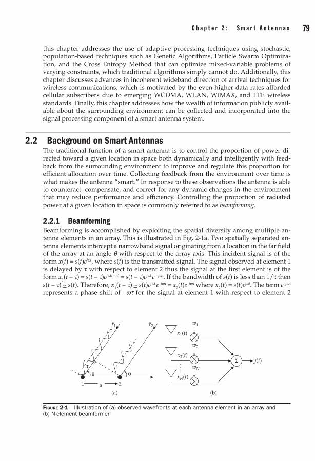
78 F r o n t i e r s i n a n t e n n a s : N e x t G e n e r a t i o n D e s i g n & e n g i n e e r i n g C h a p t e r 2 : S m a r t a n t e n n a s 79
this chapter addresses the use of adaptive processing techniques using stochastic, population-based techniques such as Genetic Algorithms, Particle Swarm Optimiza-tion, and the Cross Entropy Method that can optimize mixed-variable problems of varying constraints, which traditional algorithms simply cannot do. Additionally, this chapter discusses advances in incoherent wideband direction of arrival techniques for wireless communications, which is motivated by the even higher data rates afforded cellular subscribers due to emerging WCDMA, WLAN, WIMAX, and LTE wireless standards. Finally, this chapter addresses how the wealth of information publicly avail-able about the surrounding environment can be collected and incorporated into the signal processing component of a smart antenna system.
2.2 Background on Smart AntennasThe traditional function of a smart antenna is to control the proportion of power di-rected toward a given location in space both dynamically and intelligently with feed-back from the surrounding environment to improve and regulate this proportion for efficient allocation over time. Collecting feedback from the environment over time is what makes the antenna “smart.” In response to these observations the antenna is able to counteract, compensate, and correct for any dynamic changes in the environment that may reduce performance and efficiency. Controlling the proportion of radiated power at a given location in space is commonly referred to as beamforming.
2.2.1 BeamformingBeamforming is accomplished by exploiting the spatial diversity among multiple an-tenna elements in an array. This is illustrated in Fig. 2-1a. Two spatially separated an-tenna elements intercept a narrowband signal originating from a location in the far field of the array at an angle q with respect to the array axis. This incident signal is of the form x(t) = s(t)ejwt, where s(t) is the transmitted signal. The signal observed at element 1 is delayed by τ with respect to element 2 thus the signal at the first element is of the form x1(t – t) = s(t – t)ejw(t – t) = s(t – t)ejwt e –jwt. If the bandwidth of s(t) is less than 1/t then s(t – t) ~ s(t). Therefore, x1(t – t) ~ s(t)ejwt e–jwt = x2(t)e
–jwt where x2(t) = s(t)ejwt. The term e–jwt
represents a phase shift of –wt for the signal at element 1 with respect to element 2
(a) (b)
Σ
w1
w2
wN
x1(t)
x2(t)
xN(t)
y(t)...
r1 r2
θ
1 2
τθ
d
Figure 2-1 Illustration of (a) observed wavefronts at each antenna element in an array and (b) N-element beamformer
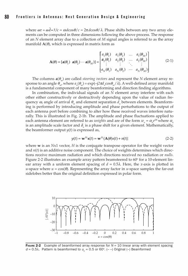
80 F r o n t i e r s i n a n t e n n a s : N e x t G e n e r a t i o n D e s i g n & e n g i n e e r i n g C h a p t e r 2 : S m a r t a n t e n n a s 81
where ωτ ω= •v vd r c/ = w dcosq/c = 2π dcosq/l. Phase shifts between any two array ele-
ments can be computed in three dimensions following the above process. The response of an N element array due to a collection of M signal angles is referred to as the array manifold A(q), which is expressed in matrix form as
A a a a( )θ θ θ θ
θ θ θ
= [ ]( ) ( ) ( )
( ) ( ) ( )
1 2
1 1 1 2 1
L
K
M
Ma a a
= aa a a
a a a
M
N N N M
2 1 2 2 2
1 2
( ) ( ) ( )
( ) ( ) ( )
θ θ θ
θ θ θ
K
M M O ML
(2-1)
The columns a(qm) are called steering vectors and represent the N element array re-sponse to an angle qm, where an(qm) = exp(–j2pdncosqm/l). A well-defined array manifold is a fundamental component of many beamforming and direction finding algorithms.
In combination, the individual signals of an N element array interfere with each other either constructively or destructively depending upon the value of radian fre-quency w, angle of arrival qm and element separation dn between elements. Beamform-ing is performed by introducing amplitude and phase perturbations to the output of each antenna port before combining to alter how these received waves interfere natu-rally. This is illustrated in Fig. 2-1b. The amplitude and phase fluctuations applied to each antenna element are referred to as weights and are of the form wn = ane
jdn where an
is an amplitude scale factor and dn is a phase shift for a given element. Mathematically, the beamformer output y(t) is expressed as,
y t t s t n tH H( ) ( ) ( ) ( ) ( ))= = +w x w A( θ (2-2)
where w is an Nx1 vector, H is the conjugate transpose operator for the weight vector and n(t) is an additive noise component. The choice of weights determines which direc-tions receive maximum radiation and which directions received no radiation or nulls. Figure 2-2 illustrates an example array pattern beamsteered to 60o for a 10-element lin-ear array with a uniform element spacing of d = 0.5l. Here, the x-axis is plotted in u-space where u = cos(q). Representing the array factor in u-space samples the far-out sidelobes better than the original definition expressed in polar form.
–1 –0.8 –0.6 –0.4 –0.2 0 0.2 0.4 0.6 0.8 1–30
–20
–10
0
10
u = cos(θ)
|A
F(u)
|
Figure 2-2 Example of beamformed array response for N = 10 linear array with element spacing d = 0.5λ. Pattern is beamformed to u
o = 0.5 or 60o. (– –) Original (–) Beamformed

80 F r o n t i e r s i n a n t e n n a s : N e x t G e n e r a t i o n D e s i g n & e n g i n e e r i n g C h a p t e r 2 : S m a r t a n t e n n a s 81
The system architecture formed from the combination of antenna array, weights, and combiner is referred to as a beamforming network. Beamforming networks can be analog or digital in nature. Analog beamforming networks are constructed from pas-sive components such as phase shifters, transmission lines, lenses, waveguides, micro-wave printed circuits, power dividers/combiners, and hybrid junctions. In combina-tion, these elements act to manipulate the amplitude and phase between elements of the array. A typical example of an analog beamformer is the Butler matrix. The Butler matrix is designed to produce multiple spot beams that point at different fixed angles. Figure 2-3a illustrates a four-element Butler matrix. It consists of several phase shifters and quadrature hybrid junctions for creating the fixed beams. The number of antenna elements determines the angular direction of the fixed beam mainlobe which is evenly distributed around q = 0o. For a spacing d = l/2, the beams are equally spaced over a span of 180o. Modern Butler matrices can be implemented on printed circuits boards and are an effective means for developing fixed beams for narrowband applications.
45°
3 1 4 2
QuadratureHybrid
Phase Shifter
45°
–90°–90°
–90°–90°
–90° –90°
–90° –90°
1
2 3
4
(a) (b)
Figure 2-3 (a) Butler Matrix and switched beams and (b) Rotman Lens and instantaneous currents for excited beamport [1]. (Courtesy J. Dong, et. al © ACES 2009)

82 F r o n t i e r s i n a n t e n n a s : N e x t G e n e r a t i o n D e s i g n & e n g i n e e r i n g C h a p t e r 2 : S m a r t a n t e n n a s 83
Another popular analog beamformer is the Rotman lens shown in Fig. 2-3b. The Rotman lens is different from the Butler matrix in that it is constructed from a parallel-plate structure usually formed as a strip-line conductor. When a given port is excited the true time delay for the EM wave to propagate across the parallel-plate region deter-mines the arrival phase and amplitude at the output ports that are fed to the array ele-ments. This is illustrated by the instantaneous current distribution in Fig. 2-3b. Exciting different ports changes the observed amplitude and phase at each output of the array. As a result, the total array pattern interferes differently between each excited beam port, resulting in multiple spot beams at different angular directions similar to that of the Butler matrix. The Rotman lens is a desirable beamforming network for many applica-tions due to its ease of construction, low cost, and light weight.
In digital beamforming networks the received signal at each element is sampled then downconverted to baseband and output as I/Q data streams. These I/Q data streams represent the digitized amplitude and phase of the incident signal at each ele-ment over time. These digitized signals are forwarded to a signal processing engine made up of computers, field-programmable gate arrays, and graphical processing units where the processes of phase shifting, amplitude scaling, and element combining are carried out in software. The ultimate benefit in implementing a digital beamformer is its flexibility. A single array can form, steer, and shape multiple beams simultaneously toward multiple directions unlike the analog beamformer which has only a few fixed beams from which to choose. Any number of signal processing techniques and algo-rithms can be used to carry out beamforming on the digitized signals. A typical adap-tive array configuration is shown in Fig. 2-4. Here, an error signal e(k) is the input to the beamforming algorithm created from a combination of the array output y(k) and some known signal feature s(k). The beamforming algorithm updates the weights and per-forms iteratively to form the beamformed output. A typical beamforming algorithm for this configuration is Widrow’s least mean squares (LMS) algorithm [2]. The LMS algorithm
.
x1(k)
s(k)
x2(k)
.
.
y(k)
BeamformingAlgorithm
e(k)
wN*
w2*
w1*
(–)
(+)
Σ
Σ
xN(k)
Figure 2-4 Typical adaptive array configuration. The array weights are updated using an error signal e(t) created from a combination of the array output y(t) and some known signal feature d(t).

82 F r o n t i e r s i n a n t e n n a s : N e x t G e n e r a t i o n D e s i g n & e n g i n e e r i n g C h a p t e r 2 : S m a r t a n t e n n a s 83
is a gradient-based iterative optimization algorithm based on the steepest descent method. The weight update equation for the LMS algorithm is given by
w w x( ) ( ) ( ) ( )*k k e k k+ = +1 µ (2-3)
where e k s k y k s k kH( ) ( ) ( ) ( ) ( )= - = - w x is the error signal, μ is the step-size parameter.The LMS algorithm iteratively solves for the array weights. The convergence of the
algorithm is guided by the choice of step-size parameter. A small step-size parameter slows the speed of the algorithm.
As an example, the LMS algorithm was employed to adaptively steer the array pat-tern of an N = 8 uniform linear array with spacing d = 0.5l. Incident upon the array are two signals, one of the form cos(wt) where w = 2πf for f = 2 kHz and the other a random sequence whose values were sampled from a Gaussian distribution of zero mean and unit variance. The desired signal to beamform toward is defined as s(k) = cos(wk) where k = nts for ts = 10 ms and 100 samples. The desired signal is incident upon the array at an angle of 30o whereas the random Gaussian sequence is considered as the interferer to be nulled with an arrival angle of –60o. Additionally, additive white Gaussian noise is pres-ent with an SNR of 10 dB and the step-size parameter of the LMS algorithm was set to 0.02. Each sample k of the array output y(k) is fed to the LMS algorithm for determining the adapted weights using (2-3). The results of the simulation are shown in Fig. 2-5. Figure 2-5a illustrates the beamformed array pattern. Clearly, the mainlobe has been shifted to point at the desired signal arriving at 30o and a null of –20 dB has been placed toward the interferer at –60o. Figure 2-5b shows the mean square error between the desired signal and the array output as a function of iteration or sample number. The error settles to a value oscillating about 1e-3 after about 30 iterations. Figure 2-5c depicts the desired signal and the array output overlapped to show the convergence of the array output as the array pattern is beamsteered toward the desired signal. After approxi-mately 30 iterations the array output and desired signal are indistinguishable. Essen-tially, the LMS algorithm has improved the SNR of the received signal and removed the contribution of the interfering signal to the array output.
2.2.2 Direction-of-Arrival Estimation TechniquesThe fundamental operation of smart antennas relies on a well-defined sense of what direction to focus the array response toward. How these directions and the resulting weights are computed has been a topic of research for over 60 years. If the angle of interest qo is known a priori then one can compute a normalized weight vector where wHw = 1 such that the beamformer gain is maximized in that direction and valued at unity. Given that y(t) = wHA(q) the weight vector that produces y(t) = 1 at qo is w a a a= ( ) ( ( ) ( ))θ θ θo
Ho o such that y t H
oH
o oH
o o( ) ( ) ( ) ( ) ( ( ) ( ))= = =w a a a a aθ θ θ θ θ 1. To simul-taneously beamform toward multiple directions of interest with the above equation one solves w AH ( )θ = u by inverting A(q) to yield wH = uA(q)–1. Here u is a row vector of constants representing the desired beamformer output at that angle. In order to invert A(q) it is required that the number of elements in the array equal the number of direc-tions. If the number of elements is less than the number of directions then a pseudo-inverse of A(q) can be performed,
A AA IH Hn( + -σ 2 1) (2-4)
where a small value sn2 is added to the diagonals of AAH to prevent the inversion of the
matrix product from being singular.
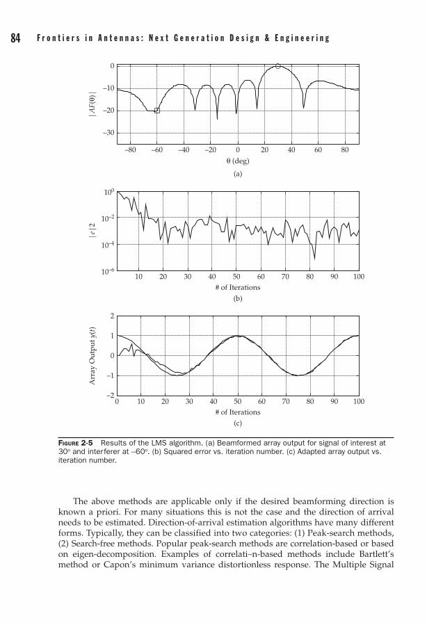
84 F r o n t i e r s i n a n t e n n a s : N e x t G e n e r a t i o n D e s i g n & e n g i n e e r i n g C h a p t e r 2 : S m a r t a n t e n n a s 85
The above methods are applicable only if the desired beamforming direction is known a priori. For many situations this is not the case and the direction of arrival needs to be estimated. Direction-of-arrival estimation algorithms have many different forms. Typically, they can be classified into two categories: (1) Peak-search methods, (2) Search-free methods. Popular peak-search methods are correlation-based or based on eigen-decomposition. Examples of correlati–n-based methods include Bartlett’s method or Capon’s minimum variance distortionless response. The Multiple Signal
–80 –60 –40 –20 0 20 40 60 80
–30
–20
–10
0
θ (deg)
|AF(
θ)|
(a)
10 20 30 40 50 60 70 80 90 10010–6
10–4
10–2
100
# of Iterations
|e|2
(b)
0 10 20 30 40 50 60 70 80 90 100–2
–1
0
1
2
# of Iterations
Arr
ay O
utpu
t y(t
)
(c)
Figure 2-5 Results of the LMS algorithm. (a) Beamformed array output for signal of interest at 30o and interferer at -60o. (b) Squared error vs. iteration number. (c) Adapted array output vs. iteration number.

84 F r o n t i e r s i n a n t e n n a s : N e x t G e n e r a t i o n D e s i g n & e n g i n e e r i n g C h a p t e r 2 : S m a r t a n t e n n a s 85
Classification (MUSIC) estimate is an example of an eigen-decomposition based meth-od. Popular search-free methods include Root-Music and ESPRIT. The reader is referred to [3], [4] for a more thorough treatment on the subject.
Most of these methods rely on two components for computing the direction-of-arrival: (1) A well defined array manifold and (2) A good estimate of the covariance matrix of the array response. Typically, the array manifold undergoes a calibration procedure to measure the array steering vectors for a given direction-of-arrival. The covariance matrix, R is formed from the complex response of each port in the array. The covariance matrix is an NxK matrix defined as R = x∙xH/K, where x is as defined in (2-2) and K represents the number of samples. This value can be averaged over several sample blocks of size K to help reduce the effects of noise on the covariance estimate; however, one must be careful that noise is stationary and ergodic over the duration of the block size.
In correlation-based methods, the estimated covariance matrix R constructed from the measured array response x is correlated against the calibrated array response a(q) to produce a correlation coefficient over all angles of interest qm resulting in a correlation surface. The direction-of-arrival is then attributed to the peak of the correlation surface. An example correlation surface is shown in Fig. 2-6. Here, the Bartlett method was used and is defined as
Ctr
H
H( )
( )( )
( ) ( )θ θ θ
θ θ=
1R
a Raa a( )
(2-5)
Interpolating the peak of the correlation slice is done to accurately capture the frac-tional value of the direction-of-arrival. The broad line along the diagonal represents the width of the mainlobe of the correlation surface indicating regions of high correlation corresponding to the direction of arrival. Brighter regions on either side of the diagonal represent sidelobes in the estimate, which could result in false estimates of the direction of arrival. Figure 2-6b shows a slice through the correlation surface in Fig. 2-6a along the x-axis for a y-axis value of 29o. The noise present in the system is evident due to the jagged nature of consecutive x-axis slices. This results in some uncertainty in the true
Azimuth - deg
Azi
mut
h - d
eg
50 100 150 200 250 300 350
50
100
150
200
250
300
350
0 100 200 3000.5
0.6
0.7
0.8
0.9
1Slice at 29 deg
Azimuth - deg
Cor
rela
tion
Coe
ffic
ient
0.4
0.5
0.6
0.7
0.8
0.9
1
(a) (b)
Figure 2-6 Example correlation surface for correlation-based direction-of-arrival estimation. (a) Correlation surface. (b) Slice through correlation surface for incoming angle of 29o.

86 F r o n t i e r s i n a n t e n n a s : N e x t G e n e r a t i o n D e s i g n & e n g i n e e r i n g C h a p t e r 2 : S m a r t a n t e n n a s 87
location of the direction-of-arrival. As such, a Monte Carlo simulation is performed and the rms error is computed for each direction-of-arrival.
Eigen-decomposition methods typically have much higher resolution than their correlation-based counterparts and as a result are often referred to as super-resolution techniques. The most popular eigen-based method is Schmidt’s MUSIC estimate. In MUSIC, an eigenvalue decomposition is performed on the covariance matrix R and two orthogonal subspaces are created, one for the signal and another for the noise. The basic principle is to extract the eigenvectors associated with the smallest eigenvalues which correspond to the noise subspace. The noise subspace is orthogonal to the array steering vectors at a given direction-of-arrival and thus are in the null-space of the noise sub-space. A projection of the steering vectors onto the noise subspace, a E E a( ) ( )θ θH
n nH re-
sults in a value of zero. Placing this expression in the denominator creates sharp peaks at the direction-of-arrival.
Often it is undesirable to perform a peak search and interpolation to find the direc-tion-of-arrival. As a result, search-free methods have been developed. Two popular ex-amples of search-free methods include Root-MUSIC and ESPRIT (Estimation of Signal Parameters via Rotational Invariance Technique). In Root-MUSIC, the peak search of the original MUSIC estimate is replaced by solving for the roots of a polynomial. Gener-ally this method results in more accurate estimates of the direction-of-arrival; however, the original MUSIC estimate can be applied to any array geometry, whereas the Root-MUSIC algorithm is applied only to uniform linear arrays. ESPRIT constrains the array geometry by requiring arrays comprised of two identical sub-arrays of the same orien-tation. Extensions of Root-MUSIC and ESPRIT to more general array geometries have been developed such as UCA Root-MUSIC and UCA ESPRIT for uniform circular ar-rays, the Rank Reduction Estimator (RARE) [5], generalized ESPRIT [6], and Fourier-Domain Root MUSIC [7].
The remaining materials presented in this chapter are extensions of the principles discussed in this introduction and represent frontiers in smart antenna signal process-ing. The two fundamental components of smart antennas, namely adaptive signal pro-cessing and direction-of-arrival estimation, are addressed. Section 2.3 focuses on the use of stochastic, population based algorithms such as Genetic Algorithms, Particle Swarm Optimization, and the Cross Entropy Method for performing adaptive beam-forming and nulling. Section 2.4 presents material about new direction-of-arrival tech-niques for wideband signal processing, and finally Section 2.5 introduces concepts for knowledge-aided smart antennas, which use information collected from the surround-ing environment to help guide the smart antenna.
2.3 Evolutionary Signal Processing for Smart AntennasEvolutionary signal processing refers to algorithms with multiple agents (such as particles, chromosomes, probability density functions) that interact intelligently with one another, but operate autonomously and progress in a cooperative fashion toward the solution of a complex problem. The implementation of evolutionary signal processing algorithms in smart antenna systems is the focus of this section. Considered here are evolutionary opti-mization algorithms based on the growth of a population and guided by stochastic prin-ciples toward a solution. There exist many algorithms that fit this definition, but special attention is paid to two types of algorithms. First those centered around the evolutionary, biological, and cognitive processes of nature and secondly those whose population samples are derived from an evolving probability distribution.

86 F r o n t i e r s i n a n t e n n a s : N e x t G e n e r a t i o n D e s i g n & e n g i n e e r i n g C h a p t e r 2 : S m a r t a n t e n n a s 87
Examples of algorithms based on the evolutionary, biological, and cognitive pro-cesses of nature are
Genetic Algorithms• (GA) Developed by John Holland in the 1960s and 1970s, it is an algorithm based on Charles Darwin’s theory of natural selection and biological evolution.
Particle Swarm Optimization• (PSO) Developed by James Kennedy and Russell Eberhart in 1995, it based on the cognitive behavior between individuals in a swarm. For example, such swarms could be schools of fish or flocks of birds.
Ant Colony Optimization• (ACO) Developed by Marco Dorigo in 1992, it is based on how ants forage for food through their interaction with pheromones and scent chemicals to help promote the optimum path to the food source for others to follow.
Simulated Annealing • (SA) Based on the annealing process of materials.
Harmony Search • (HS) Based on the aim of musicians to search for a harmonious state.
Bees Algorithm• (BA) Based on the behavior of honey bees and pollination.
Firefly Algorithm• (FA) Based on the communication role of bioluminescent interaction between fireflies while mating.
Bacterial Foraging Algorithms • [8] Inspired by the foraging behavior of Escherichia (E.) coli bacteria in the human intestine.
The algorithms described above all have the same basic structure, but differ slight-ly in their implementation, which affects convergence speed and solution accuracy.
Specific attention will be given primarily to Genetic Algorithms and Particle Swarm Optimization due to their overwhelming popularity, hybridization, and improvements thereon. Algorithms whose population samples are derived from an evolving probabil-ity distribution include
Markov Chain Monte Carlo• (MCMC) Sampling from a probability distribution is accomplished by constructing a Markov Chain. The state of the chain is updated from one iteration to the next until an equilibrium state is met, which represents the optimal probability distribution.
Cross Entropy Method• (CEM) The parameters of a probability distribution are updated by minimizing cross-entropy or Kullback-Leibler divergence between two probability distributions.
Specific attention will be given to the Cross Entropy Method, which has been shown to be a powerful optimization technique for finding solutions of rare-event processes as well as optimizing multiextremal, multiobjective functions. A key feature of the CEM is that it is based on the updating of a parameterized probability distribution, which car-ries information about the current best solutions from one iteration to the next. All subsequent optimization is carried out on the probability distributions that define each variable in the solution space and not on the individual solutions in the population such as is done in Genetic Algorithms and Particle Swarm Optimization.
The application of population-based stochastic algorithms for solving electromag-netic optimization problems has been a popular area of research for the last 15 years. In particular, literature published on the application of GA, PSO, and variants thereof to

88 F r o n t i e r s i n a n t e n n a s : N e x t G e n e r a t i o n D e s i g n & e n g i n e e r i n g C h a p t e r 2 : S m a r t a n t e n n a s 89
the array pattern synthesis problem is extensive; however, much of the work cannot be directly applied to adaptive signal processing due to the associated fitness functions used for performing pattern synthesis. The frontier in smart antennas is in the imple-mentation of these algorithms for adaptive updating of weights in place of the more conventional methods based on convex/quadratic/nonlinear programming, least squares, or gradient-descent subject to available real-world feedback from the array output. Pioneering literature has been published on this subject by Randy Haupt of Penn State, but its application has been somewhat limited in part due to the perception that stochastic algorithms are slow to converge and cost too much to compute com-pared to conventional methods and therefore are not suitable for incorporation into adaptive systems such as smart antennas. Another fear is that the optimization objec-tive, say for example SINR maximization in a cellular network, will change too quickly as mobile users traverse the cell and the algorithms do not have the capability to detect nor adapt to these changes since the algorithms are still trying to solve for the original objective. Advancements in computational speed and memory loading can alleviate some of this, but for the most part the algorithms need to be constrained and modified for application in smart antennas. Researchers have introduced modified algorithms with improved convergence speeds and objective function interjections to address changing objectives. This section highlights these improvements for the algorithms detailed above as well as demonstrates some simple examples and provides a cursory comparison.
The advantages of population-based stochastic algorithms include the following characteristics:
Optimization with a mixture of discrete and continuous variables. Discrete •optimization can be the result of encoding the continuous variables. Mixtures can contain binary values, integers, etc.
A wide area of the feasible region is searched by generating a population of •candidate solutions, and then the algorithm converges toward a local neighborhood of the global optimum solution.
By using a population of candidate solutions, parallel processing on multiple •platforms is possible.
Multiextremal, multiobjective, multivariable optimization problems can be •solved without the use of derivative information.
It is possible to avoid trappings of local extrema.•
Nonlinear fitness functions can be used which are not applicable to conventional •algorithms.
One does not need to be an expert on the physics of the antenna array nor of the •surrounding environment in order to exploit it.
In general, population–based stochastic algorithms can be summarized by a two-step iterative procedure:
1. First, a population of candidate solutions is sampled from a random variable, which closely models the structure of the problem and constrained to a feasible region of interest.
2. Second, the sampling of the population is updated using a subset of the current best solutions to ensure those samples appear in subsequent iterations and contribute to the generation of future solutions.

88 F r o n t i e r s i n a n t e n n a s : N e x t G e n e r a t i o n D e s i g n & e n g i n e e r i n g C h a p t e r 2 : S m a r t a n t e n n a s 89
In the first step, a number of candidate solutions are sampled from a random vari-able and compiled to form a population X, which is a matrix whose columns represent a single sample set of a variable for optimization and whose rows are the collection of sample set variables for a single candidate solution. For example, say we have N = 2 variables, y and z, for optimization. A population size of M is chosen, so the population X is represented as,
X y z= =
[ ]
( ) ( )( ) ( )
( ) ( )
y zy z
y M z M
1 12 2M M
(2-6)
Given some deterministic scoring function S(X) each row in the population X is evaluated. If the scoring function is of the form S(x) = y+z, then X is scored as
S S
S y zS y z
S y M
( ) ([ ])
( ( ), ( ))( ( ), ( ))
( (
X y z= =
1 11 2M)), ( ))
( ) ( )( ) ( )
(z M
y zy z
y M
=
++
1 12 2
M)) ( )+
z M
(2-7)
Each of the rows of S(X) is evaluated as to its fitness to an overall objective, depend-ing on whether the objective is to maximize or minimize the population’s response to the scoring function. A subset of the best performing candidates is then used to gener-ate the new population in the next iteration. In the cases of Genetic Algorithms and Particle Swarm Optimization this is done by performing operations on the candidates in the population, whereas with the Cross Entropy Method each column is represented by a probability distribution and the best candidates are used to update the estimate of this probability distribution.
2.3.1 Description of Algorithms
2.3.1.1 The Genetic AlgorithmThe Genetic Algorithm (GA) was developed by John Holland in the 1960s and 1970s. It is based on Charles Darwin’s theory of natural selection and biological evolution. The application of the genetic algorithm to electromagnetic optimization problems and in particular to pattern synthesis problems has been an active area of research since the 1990s. Randy Haupt of Penn State University’s Applied Research Lab has been at the forefront of this research. His work and others is nicely summarized in his book entitled Genetic Algorithms in Electromagnetics published by Wiley [9].
The fundamental principle of Genetic Algorithms involves encoding optimization variables into strings called chromosomes. A collection of chromosomes form a popula-tion. The fitness of these chromosomes to some objective function is computed and new candidate solutions, called offspring, are created through genetic operators called cross-over and mutation. Crossover is performed between pairs of chromosomes in the popu-lation, called parents, in which genetic information is exchanged in order to produce offspring of a new generation. Crossover seeks to propagate the chromosomes of par-ents with high fitness into the future to ensure improvement of solutions in subsequent iterations.
Mutation introduces random changes into the population. Mutation ensures that the population is not entirely uniform as the algorithm approaches a solution and allows

90 F r o n t i e r s i n a n t e n n a s : N e x t G e n e r a t i o n D e s i g n & e n g i n e e r i n g C h a p t e r 2 : S m a r t a n t e n n a s 91
the algorithm to continue to search for better results. The rate of mutation is often very low and the primary mechanism for improving the overall fitness is crossover. The strategies for choosing which parents and how many perform crossover have a big impact on the success of the algorithm.
There are two main strategies, namely roulette wheel and tournament selection. In roulette wheel, each chromosome is assigned a probability based on its rank in the population. Rank can be determined by either its position in the population or by its fitness to the objective function. The probability of a given chromosome being chosen for mating is based on this rank. Higher ranks receive higher probabilities of selection. The probability of selection is reduced as the size of the mating pool is increased, how-ever. Random numbers are drawn from a uniform distribution and compared to the probabilities assigned to each parent to form the mating combinations. This process is continued until a certain percentage of the population has been replaced with new off-spring. In tournament selection, several chromosomes are selected randomly and formed into a group. The chromosome with the lowest cost is chosen as a parent. The tournament is continued until all offspring have been created.
Typically, the elements of the chromosomes are binary in nature, but modern ge-netic algorithms can account for mixed-integer chromosomes as well [13]. The mixture of integers, real and binary variables, is performed within the objective function so that the structure of the algorithm remains unchanged. Encoding variables into binary representations increases the dimension of the problem. The population size, selection of mates, and mutation rate are the biggest factors influencing the convergence rate of the algorithm. If the population size it too small, then there is a risk of the population going extinct since the population fails to evolve. Using the most elite chromosomes for reproducing ensures the most fit individuals will be carried to the next generation, but too few will result in stagnation. Mutation of a single variable is not enough to search the space efficiently. Multiple mutations are more effective, but if there are too many mutations the algorithm will not converge. A summary of the selection param-eters is given in [9]. Therein, the author cites the work of DeJong [11] and Grefenstette [12]. The result of their combined work determined that best results were achieved with a population size of 20 to 30, a crossover rate of 75 to 95% of the population, with mutation occurring about 1% of the time. It is intuitive that early on in the evolution process a large number of mutations helps to explore the solution space; however, over time this value should be decreased to allow crossover to take over. The algorithm is halted once the fitness of the population is below some threshold, the algorithm has stalled due to uniformity from successive crossovers, or a maximum number of evalu-ations has been reached.
In summary, the genetic algorithm can be summarized by the following steps:
1. Generate population
a. A population of candidate solutions or chromosomes is constructed from random samples of a probability distribution.
2. Create mating pool, perform selection and reproduce offspring
a. Encode chromosomes of population into binary strings.
b. Evaluate fitness of the population and rank.
c. Draw probabilities for parents to determine selection for reproduction.
d. Reproduce offspring through crossover.

90 F r o n t i e r s i n a n t e n n a s : N e x t G e n e r a t i o n D e s i g n & e n g i n e e r i n g C h a p t e r 2 : S m a r t a n t e n n a s 91
3. Perform mutation
a. Draw a random number from a uniform distribution. If this random number exceeds some threshold, then perform mutation. Otherwise, the population remains unchanged.
4. Set t = t+1 and repeat steps 1 through 3 until the stopping criterion is satisfied.
2.3.1.2 Particle Swarm OptimizationParticle Swarm Optimization (PSO) [10] was developed by James Kennedy and Russell Eberhart in 1995. It is based on the intelligent interactions between individuals in a swarm to achieve an objective. Examples of such swarms are schools of fish or flocks of birds. The swarm acts cooperatively to achieve this objective; however, individual com-ponents of the swarm (called particles) behave independently and are influenced by their social interactions with one another. The composite trajectory of an individual agent in the swarm has deterministic and stochastic components. The deterministic mo-tion is governed by the global trajectory of the swarm, but the individual maintains freedom to wander locally at random. Its rate of change in a given direction is influ-enced by its neighbors as well as the swarm as a whole. It has memory of its best posi-tions as well as knowledge of the best positions of all particles within the swarm. Over time, the particles of the swarm discover improvements upon the objective and share these discoveries with all other particles in the swarm, first locally and then propagated globally.
Consider an individual particle with a 1xN position vector xt and velocity vector vt at time t. This particle searches through a feasible region of possible solutions for the optimum position g* while remembering its previous best positions p. The future veloc-ity of the particle vt +1 on its way to g* is formed by perturbing its current velocity by the distance between its best known position pt and current position xt. This is represented as vt+1 = vt + c1∙r1∙(p – x), where c1 is a positive constant influencing the acceleration to the new position and where r1 is a vector of uniformly distributed random perturbations in the range [0,1] to encourage wandering. The new position is then computed as xt+1 = xt + vt+1. The particle compares this new position to its current best p and replaces p with xt+1 if it results in an improved fitness to the objective. This particle is a component of the swarm and is subject to influence from its neighbors as well as the rest of the swarm. The swarm’s knowledge of its global best position g influences individual particles by adjusting vt+1 by c2∙r2∙(g – x), where c2 is a positive constant and r2 is a vector of uni-formly distributed random values in the range [0,1]. Neighbors of particles exert influ-ence through the term c3∙r3∙(b – x) where b is the best known position of its K nearest neighbors. Neighbors can be defined in terms of their Euclidean distance in the search space, fitness to the objective function or location in X. Typical values for c1, c2 are cho-sen equal to 2 whereas c3 is chosen equal to 1. Together, the total update of the velocity and position of each particle is performed as
v v r p x r g x r bt t t tc c c+ = + ⋅ ⋅ - + ⋅ ⋅ - + ⋅ ⋅ -1
1 1 2 2 3 3( ) ( ) ( xx
x x v
t
t t t
)
+ += +1 1 (2-8)
The velocity updates for the entire swarm of M particles with size N is represented by the MxN matrices V and X whose rows are formed from (1-8). In general, the swarm is collectively influenced by the global best position and individually influenced by

92 F r o n t i e r s i n a n t e n n a s : N e x t G e n e r a t i o n D e s i g n & e n g i n e e r i n g C h a p t e r 2 : S m a r t a n t e n n a s 93
their memory of previous best positions and those of its nearest neighbors. The influ-ence of neighbors is sometimes omitted to improve convergence, and influence is ex-erted only by the global best position of the swarm. As the swarm converges to the optimum solution xt = g*. Typically, this is not achieved, rather the particles of the swarm converge to a local neighborhood of the optimum solution and continue to search until forced to stop. This can cause the velocities to explode unless they are limited in some way. Typically, a bound is placed on the maximum velocity the algorithm can achieve. This limits the search area of the algorithm and prevents explosion of velocity values. Additionally, an inertial weight can be added to velocities, which forces the particles to slow down as they get close to the optimum solution and search only in a small area. In summary, the two typical methods for constraining velocities are,
1. Bounds on velocity
If vnt > vmax then set vn
t = vmax
If vnt < –vmax then set vn
t = –vmax
2. Inertial weighting
v v r p x r g x rt t t tw c c c+ = ⋅ + ⋅ ⋅ - + ⋅ ⋅ - + ⋅ ⋅11 1 2 2 3 3( ) ( ) (bb x- t )
where w is a positive constant less than one or a function that decreases over time. In summary, the PSO algorithm can be summarized by the following steps.
1. Initialize Parameters:
a. MxN matrices V0 and X0 for the velocities and locations of the swarm particles. The elements of X0 are sampled from a uniform distribution in the range [a,b] where –∞ < a, b < ∞. Initial velocities are set equal to zero.
b. MxN matrices for the global best G and local best P positions of the swarm. The rows of G are set to arg minf(x0) where x0 is the best performing particle in X. The elements of P are set equal to X0.
c. Mx1 objective function f(P) and the scalar f(G).
d. Set iteration counter t = 1.
2. Generate the MxN matrices R1 and R2 whose elements are sampled from a uniform distribution in the range [0, 1].
3. Update the particle velocities by
V V R P X R G Xt t t tw c c+ = + ⋅ ⋅ - + ⋅ ⋅ -11 1 2 2( ) ( )
where multiplications are performed element-wise.
4. Update the particle positions by
X X Vt t t+ += +1 1
5. If f(Xt+1) < f(P), update local best positions P with Xt + 1.
6. If f(xt+1) < f(G), update the rows of the global best positions G with xt+1, where xt+1
is the best performer in Xt+1.
7. Set t = t+1 and repeat steps 2 through 6 until the stopping criterion is satisfied.

92 F r o n t i e r s i n a n t e n n a s : N e x t G e n e r a t i o n D e s i g n & e n g i n e e r i n g C h a p t e r 2 : S m a r t a n t e n n a s 93
The general formulation of PSO presented above is typically performed on continu-ous variables. For discrete problems of binary variables, a slight modification is intro-duced. The velocities of [?] are evaluated to form a probability threshold s(v) chosen as the sigmoid function from neural networks
s( )exp( )
vv
=+ -
11
(2-9)
The vector s(v) is used to decide whether the elements of x are assigned values of 1 or 0. The decision is made by drawing a vector of random numbers ρ from a uniform distribution in the range [0,1]. If an element of ρ is less than its corresponding element in s(v) then its corresponding element in x is assigned a 1, else it is assigned a 0.
2.3.1.3 Cross Entropy MethodThe Cross Entropy Method (CEM) is a general stochastic optimization technique based on a fundamental principle of information theory called cross entropy (or Kullback-Leibler divergence) [14], [15]. CEM was first introduced in 1997 by Reuven Y. Rubin-stein of the Technion, Israel Institute of Technology as an adaptive importance sampling for estimating probabilities of rare events [16] and was extended soon thereafter to in-clude both combinatorial and continuous optimization [17]. The CEM has successfully optimized a wide variety of traditionally hard test problems including the max-cut problem, traveling salesman, quadratic assignment problem, and n-queen. Addition-ally, the CEM has been applied to antenna pattern synthesis, queuing models for tele-communication systems, DNA sequence alignment, scheduling, vehicle routing, learn-ing Tetris, direction of arrival estimation, speeding up the Backpropagation algorithm, updating pheromones in ant colony optimization, blind multiuser detection, optimiz-ing MIMO capacity, and many others [18]–[31]. There exist several good resources for those interested in learning more about the, CE Method [32]–[35].
To illustrate how the Cross Entropy (CE) procedure is implemented assume for the time being that the score S(x) is to be maximized over all states x ∈ X , where x = [x1,…, xM]T
is a vector of candidate solutions defined on the feasible set X. The global maxi-mum of S(x) is represented by
S x S( ) max ( )* *= =∈
γx
x (2-10)
The probability that the score function S(x) evaluated at a particular state x is close to γ* is classified as a rare event. This probability can be determined from an associated stochastic problem (ASP),
P Ev v SS I( ( ) ) ( ) x x≥ = ≥γ γ (2-11)
where Pv is the probability measure that the score is greater than some value γ close to γ*,
x is the random variable produced by a probability distribution function f(∙,v), Ev is the expectation operator and I∙ is a set of indices where S(x) is greater than or equal to γ.
Calculating the right hand side of (2-11) is a nontrivial problem and can be esti-mated using a log-likelihood estimator with parameter v,
ˆ argmax ln ( , )*) ( )v
MI f x
sS xi
s
ii
M
= ≥=∑
νγ
1
1
ν (2-12)
where xi is generated from f(∙,v), Ms is the number of samples where S(xi) > γ and Ms < M.

94 F r o n t i e r s i n a n t e n n a s : N e x t G e n e r a t i o n D e s i g n & e n g i n e e r i n g C h a p t e r 2 : S m a r t a n t e n n a s 95
As γ becomes close to γ*, most of the probability mass is close to x* and is an ap-proximate solution to (2-10). One important requirement is that as γ becomes close to γ* that Pv(S(x) > γ) is not too small, otherwise the algorithm will result in a suboptimal solution. So, there is a tradeoff between γ being arbitrarily close to γ* while maintaining accuracy in the estimate of v.
The CE method efficiently solves this estimation problem by adaptively updating the estimate of the optimal density f(∙,v*), thus creating a sequence of pairs ˆ , ˆ ( ) ( )γ t tv at each iteration t in an iterative procedure, which converges quickly to an arbitrarily small neighborhood of the optimal pair γ*, v*.
The iterative CE procedure for estimating γ*, v* is given by
1. Initialize parameters: Set initial parameter ˆ( )ν 0 , choose a small value r, set population size M, smoothing constant a, and set iteration counter t = 1.
2. Update ˆ ( )γ t :
Given ˆ( )ν t-1 , let ˆ( )γ t be the (1 – r)-quantile of S(x) satisfying
Pv( ) ( ( ) )( )t S t- ≥ ≥1 x γ ρ (2-13)
Pv( ) ( ( ) )( )t S t- ≤ ≥ -1 1x γ ρ (2-14)
with x sampled from f(∙, ˆ( )ν t-1 ). Then, the estimate of γ(t) is computed as
ˆ( )( ( ) )γ ρ
tM
S= - 1 (2-15)
where ⋅ rounds (1–r)M toward infinity.
3. Update ˆ( )ν t :
Given ˆ( )ν t-1 , determine ˆ( )ν t by solving the CE program
ˆ max ln ( , )( )) ( ˆ )( )v
MI f x vt
si
i
M
S xit
s
= ≥=∑v
1
1γ (2-16)
4. Optional step (Smooth update of ˆ( )ν t ):
To decrease the probability of the CE procedure converging too quickly to a suboptimal solution, a smoothed update of ˆ( )ν t can be computed.
ˆ ( ) ˆ( ) ( ) ( )ν αν α νt t t= + - -(1 1 (2-17)
where (v t( ) is the estimate of the parameter vector computed with (2-16), ˆ( )v t-1
is the parameter estimate from the previous iteration and a (for 0 < a < 1) is a constant smoothing coefficient. By setting a = 1, the update will not be smoothed.
5. Set t = t + 1 and repeat steps 2 through to 4 until the stopping criterion is satisfied.
What ultimately is produced is a family of pdfs f (∙, ˆ ( )v 0 ), f (∙, ˆ ( )v 1 ), f (∙, ˆ ( )v 2 ),…, f (∙, ˆ *v ) which are directed by ˆ( )γ 1 , ˆ ( )γ 2 , ˆ ( )γ 3 ,…, ˆ *γ toward the neighborhood of the optimal den-sity function f (∙, v*). The pdf f (∙, ˆ ( )v t ) acts to carry information about the best samples from one iteration to the next. The CE parameter update of (2-16) ensures that there is
94 F r o n t i e r s i n a n t e n n a s : N e x t G e n e r a t i o n D e s i g n & e n g i n e e r i n g C h a p t e r 2 : S m a r t a n t e n n a s 95
an increase in the probability that these best samples will appear in subsequent itera-tions. At the end of a run as γ is closer to γ*, the majority of the samples in x will be identical and trivially so to are the values in S(x).
The initial choice of ˆ( )ν 0 is arbitrary given that the choice of r is sufficiently small and K is sufficiently large so that Pv (S(x) > γ) does not vanish in the neighborhood of the optimal solution. This vanishing means the pdf degenerates too quickly to one with unit mass, thus freezing the algorithm in a suboptimal solution.
The preceding procedure was characteristic of a one-dimensional problem. It can be easily extended to multiple dimensions by considering a population of candidate solu-tions X = [x1,…,xN] with xn = [x1,n,…,xM,n]
T. The pdf parameter is extended to a row vector v = [v1,…,vN], which is then used to independently sample the columns of matrix X and consequently (2-16) is calculated along the columns of X.
Although the CEM was presented as a maximization problem, it is easily adapted to minimization problems by setting ˆ
( )γ ρ= S
M and updating the parameter vector
with those samples xi where S( ) ˆxi ≤ γ .The difference between discrete and continuous optimization with CE is simply the
choice of pdf used to fill the candidate population. The most typical choice of pdf for continuous optimization is the Gaussian (or Normal) distribution, where v in f(∙,v) is represented by the mean μ and variance s2 of the distribution. Other popular choices include the shifted exponential distribution, double-sided exponential, and beta distri-bution. Many other continuous distributions are reasonable, although distributions from the natural exponential family (NEF) are typically chosen since convergence to a unit mass can be guaranteed and the CE program of (2-16) can be solved analytically. The update equations that satisfy (2-12) for continuous optimization are
µ = =
=
∑
∑
I x
I
i ii
M
ii
M
s
s
1
1
, ˆ( ˆ )
σµ
2
2
1
1
=-
=
=
∑
∑
I x
I
i ii
M
ii
M
s
s (2-18)
which are simply just the sample mean and sample variance of those elite samples, I where the objective function S(xi) > γ. The worst performing elite sample is then used as the threshold parameter γ(t+1) for (2-15) in the next iteration. The result presented in (2-18) is one of the simplest, most intuitive, and versatile CE parameter estimates avail-able. In this case, as ˆ( )γ t becomes close to γ* the samples in the population will become identical, thus the variance of the sample population will begin to decrease toward zero resulting in a Gaussian pdf having unit mass about the sample mean of the population. The final location of ˆ *γ will be represented by this final mean, i.e. ˆ ˆ* *x u= as σ 2 0→ .
The CEM is modified for combinatorial optimization problems by choosing a den-sity function that is binary in nature. The most popular choice is the Bernoulli distribu-tion, Ber(p) with success probability p represented by the pdf,
f x p p p xx x; , , ( ) = -( ) ∈
-1 0 1
1 (2-19)
where f (x; p) equals p when x = 1 and 1 – p when x = 0. The update equations that satisfy (2-12) for combinatorial optimization are

96 F r o n t i e r s i n a n t e n n a s : N e x t G e n e r a t i o n D e s i g n & e n g i n e e r i n g C h a p t e r 2 : S m a r t a n t e n n a s 97
ˆ ( )
( )
pI x
I
S
S
x
x
i
s
i
s
ii
M
i
M=
≥
≥
=
=
∑
∑
γ
γ
1
1
(2-20)
An exact mathematical derivation of the convergence properties of the CEM for continuous optimization is still an open problem; however, from experience the conver-gence properties of the continuous form CEM appear similar to its combinatorial coun-terpart, but better behaved. The convergence of the combinatorial form of CE has been studied extensively and a good treatment of the theory begins with a simplified form based on parameter update by the single best performer in the population [32], [44]. More generally, the convergence properties of combinatorial optimization problems based on parameter update by the best ρK performers in the population were de-rived in [36]. The results presented were specific to problems with unique optimal solu-tions where the candidate population is evaluated by a deterministic scoring function. The main conclusion is that when using a constant smoothing parameter (as is most commonly implemented), convergence of the CEM to the optimal solution is represented by
1. The sampling distribution converging with probability 1 to a unit mass located at some random candidate x( )t ∈
And, the probability of locating the optimal solution being made arbitrarily close to one (at the cost of a slow convergence speed).
2. This is accomplished by selecting a sufficiently small value of smoothing constant, a. It is suggested that guaranteeing the location of the unique optimal solution with probability 1 can only be achieved by using smoothing coefficients, which decrease with increasing time. Examples of such smoothing sequences are
aMt t t t
t( ) ,( )
,( )log( )
,=+ + +
>1 11
1
1 11β β β (2-21)
When choosing a smoothing constant there is a trade-off between speed of conver-gence and achieving the optimal solution with high probability. Regardless, the sam-pling distribution will always converge to a unit mass at some candidate x(t) ∈X when using a smoothing constant. Generally, the speed of convergence experienced using constant smoothing parameters is generally faster than decreasing smoothing schemes. Also, for the last two smoothing techniques of (2-21) location of the optimal solution may be guaranteed with probability 1, but convergence to a unit mass with probability 1 is not. It is not known if a smoothing technique exists where both the sampling popu-lation converges to a unit mass with probability 1 and the optimal solution is located with probability 1. The authors of [36] suggest that from their experience convergence of the sampling population to a unit mass with probability one and locating the optimal solution with probability 1 are mutually exclusive events.
2.3.2 Adaptive Beamforming and Nulling in Smart AntennasAdaptive beamforming and nulling of different sources is one of the primary functions of a smart antenna in order to improve the signal-to-interference-noise (SINR) ratio of the array output. Synthesizing nulls at specific direction-of-arrivals using GA, PSO, and

96 F r o n t i e r s i n a n t e n n a s : N e x t G e n e r a t i o n D e s i g n & e n g i n e e r i n g C h a p t e r 2 : S m a r t a n t e n n a s 97
CE have been studied extensively in the literature; however, many of the techniques employed cannot be directly applied to the adaptive nulling of a smart antenna due to incomplete knowledge of the direction-of-arrival of the different interferers. Adaptive processing relies on feedback from the array output to alter the array weights in order to improve some feature of the array output. Typically, the SINR of the array output is the objective to optimize. This can be performed by measuring the output power of the array in response to desired signals and interferers incident upon the array. Addition-ally, the mean square error between the array output and some reference feature of the desired signal can be minimized as was done in Fig. 2-6.
First, consider the scenario where SINR is improved by adaptively nulling interfer-ers by measuring the output power of the array. This is the basis for the work performed by Haupt in [37]. The problem is formulated as follows. An N-element uniform linear array with spacing d has incident upon it a desired signal whose angle of arrival to the array axis falls within the mainlobe of the array pattern. At directions of arrival outside the mainlobe, several interferers are also incident upon the array. The goal is to deter-mine the optimum array weights to improve the SINR of the array output by placing nulls in the directions of the interferers by measuring the output power of the array. The array under consideration is shown in Fig. 2-7. The array contains an even number of antenna elements and the weights are applied symmetrically about the middle of the array, except that there is an odd-shift in the phase weights dn = -d-n to perform nulling [38]. The general form of the weighted array factor for this linear array is given by
AFN
w enjk n d
n
N
( ) ( ) cosθ θ= -
=∑1 1
1
, where wn = anejdn (2-22)
NullingAlgorithm
δN/2δ2δ1–δ1–δ2–δN/2
αN/2α2α1α1α2αN/2
d
Σ
s1(k), θ1s2(k), θ2
s3(k), θ3
y(t)
… …
–d/2–3d/2–(N – 1)d/2 3d/2 (N – 1)d/2d/2Array axis
Figure 2-7 Uniform linear array for adaptive nulling

98 F r o n t i e r s i n a n t e n n a s : N e x t G e n e r a t i o n D e s i g n & e n g i n e e r i n g C h a p t e r 2 : S m a r t a n t e n n a s 99
Since the array is symmetric, (2-22) can be expressed as
AFN
n kdn nn
N
( ) cos(( . ) cos )/
θ α θ δ= - +=∑2
0 51
2
(2-23)
Here, we will consider phase-only nulling (an = 1), thus there are only N/2 variables to optimize.The total output power of the array for P sources is expressed as
Power s EP AFi i ii
P
==∑20 10
1
log ( ) ( )θ θ (2-24)
where si is the signal strength of source i and EP(q) is the individual pattern of an an-tenna in the array. Here, EP(q) is set equal to one, which corresponds to omnidirec-tional antenna patterns in the q-plane. Additionally, the source power of the desired signal is also 1 or 0 dB, thus (2-24) can be simplified to
Power s EP AFi i ii
NI
==∑20 10
1
log ( ) ( )θ θ (2-25)
where NI is the number of interferers. As a result, by choosing phase weights that mini-mize the output power of the array, the interfering signals will be suppressed and the SINR of the array will be improved.
This scenario is applicable when you know the direction of the desired signal a priori, but the directions of the interferers are not known. This is a problem often en-countered in radar and jamming. For example, the radar mainlobe is pointed at the horizon to detect incoming aircraft, while jammers outside the mainlobe try to flood the receiver front end with high power noise interference. This scenario is also applicable to cellular communications scenarios where the base station has a specific direction to point its mainlobe to sectorize a geographical area, while simultaneously reducing in-terference from co-channel sources outside the mainlobe.
In order to compare GA, PSO, and CEM, the parameters shown in Table 2-1 are specified for the array, sources, and interferers.
The settings of each algorithm are summarized in Table 2-2.
Number of Sources 1
Number of Interferers 2
Source Power 0 dB
Interferer Power 30 dB
Source DOA 0o
Interferer DOA 28o, 51o
Number of Elements 40
Element Spacing 0.5λ
Table 2-1 Parameters for Adaptive Nulling Scenario

98 F r o n t i e r s i n a n t e n n a s : N e x t G e n e r a t i o n D e s i g n & e n g i n e e r i n g C h a p t e r 2 : S m a r t a n t e n n a s 99
First, the continuous forms of the algorithms for minimizing the output power of the array defined by (2-25) will be demonstrated and compared. A typical result of the optimized array pattern is shown in Fig. 2-8. The nulls at the angular locations of the two interferers are distinct and quite deep. In reality, this null depth would not be ob-served due to effects of mutual coupling between antenna elements and noise in the environment, which were not considered.
The optimization process was halted when the number of population generations exceeded 500 or if the array output power dipped below -100 dB. Typical convergence plots of the best and mean population scores for the algorithms are given in Fig. 2-9. The convergence nature displayed by GA and PSO is illustrative of what is typically encountered in the literature. The best overall score for the population is stored until a new value is found and replaces the old score. The mean overall scores for these popu-lations are quite different from each other, however. For GA, the choice of selecting four chromosomes for the mating pool and replacing all remaining chromosomes in the population tends to keep the population mean close to the global best. The mutation rate is high at a value of 0.15, so this accounts for the fluctuations in the population mean. With these choices, GA is allowed to wander the space around the global best solution in search of better solutions without diverging wildly.
–1 –0.8 –0.6 –0.4 –0.2 0 0.2 0.4 0.6 0.8 1–30
–25
–20
–15
–10
–5
0
u = cosθ
10lo
g 10|
AF|
(dB
)
OptimizedOriginal
u = 0.6293 u = 0.88295
Figure 2-8 Example optimized array pattern for adaptive nulling of interferers arriving at 28o (u = 0.8829) and 51o (u = 0.6293)
Genetic Algorithm Particle Swarm Cross Entropy
Population Size
20 Population Size
20 Population Size 20
Selection Roulette c1, c2 2,2 Smoothing Parameter, μ, σ2
1, 0.7
Cross-over Single-point Inertial weight, ω
0.2 Sample Selection parameter, ρ
0.1
Mutation rate 0.15 |νmax
| 0.1
Mating Pool 4
Table 2-2 Algorithm Settings for Adaptive Nulling Scenario
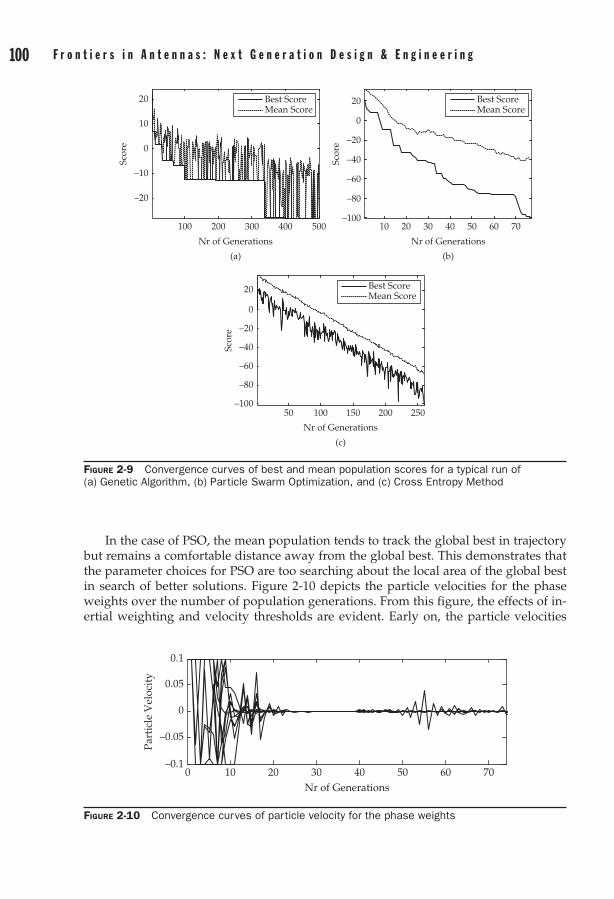
100 F r o n t i e r s i n a n t e n n a s : N e x t G e n e r a t i o n D e s i g n & e n g i n e e r i n g C h a p t e r 2 : S m a r t a n t e n n a s 101
In the case of PSO, the mean population tends to track the global best in trajectory but remains a comfortable distance away from the global best. This demonstrates that the parameter choices for PSO are too searching about the local area of the global best in search of better solutions. Figure 2-10 depicts the particle velocities for the phase weights over the number of population generations. From this figure, the effects of in-ertial weighting and velocity thresholds are evident. Early on, the particle velocities
Best ScoreMean Score
Best ScoreMean Score
100 200 300 400 500
–20
–10
0
10
20
Nr of Generations
Scor
e
10 20 30 40 50 60 70–100
–80
–60
–40
–20
0
20
Nr of Generations
Scor
e
50 100 150 200 250–100
–80
–60
–40
–20
0
20
Nr of Generations
Scor
e
Best ScoreMean Score
(a) (b)
(c)
Figure 2-9 Convergence curves of best and mean population scores for a typical run of (a) Genetic Algorithm, (b) Particle Swarm Optimization, and (c) Cross Entropy Method
0 10 20 30 40 50 60 70–0.1
–0.05
0
0.05
0.1
Nr of Generations
Part
icle
Vel
ocit
y
Figure 2-10 Convergence curves of particle velocity for the phase weights

100 F r o n t i e r s i n a n t e n n a s : N e x t G e n e r a t i o n D e s i g n & e n g i n e e r i n g C h a p t e r 2 : S m a r t a n t e n n a s 101
50 100 150 200 250
–0.4
–0.2
0
0.2
0.4
Mea
n of
Gau
ssia
n pd
f, µ
50 100 150 200 250
10–10
100
Nr of Generations
Var
ianc
e of
Gau
ssia
n pd
f, σ2
Figure 2-11 Convergence of curves for mean and variance of Gaussian distribution for each phase weight. Notice as the variance decreases the mean settle to constant values demonstrating the convergence of pdfs to a unit mass.
fluctuate and are dampened by the velocity threshold. After a few generations the iner-tial weight begins to exert influence and the algorithm quickly converges as the search area of the algorithm shrinks. This results in a small number of generations to achieve a very good solution.
In the case of CE, one can see that the trajectories of the best and mean population scores in Fig. 2-9 are linear. Given that the score function of (2-25) is a function of log10(∙), this linear nature reveals the exponential rate of convergence for which the CEM is known for. In Fig. 2-11, the mean and variance of the Gaussian probability density func-tions for the phase weights are plotted for each generation. One can see that as the vari-ance shrinks to a small value, the mean settle to a constant value, which is the final solu-tion. This is evidence of the CEM converging to a probability distribution of unit mass in which the solution is in an arbitrarily small neighborhood of the global best solution. It is clear from this example run that PSO is the best performer in terms of speed, but CE reaches a comparable score function not to far thereafter, whereas GA requires more generations to converge to an inferior value. Overall, all three algorithms can produce reasonable values for the phase weights to successfully and efficiently perform null-ing.
Since the algorithms are stochastic in nature, it is necessary to perform a Monte Carlo simulation for a number of iterations to reveal any tendencies of the algorithms. As such, 100 independent trials of the above example were conducted and the best population score of the final generation was recorded as well as the total number of generations for convergence. The results of these trials are shown in Fig. 2-12. It is evi-dent that performance of the GA could not satisfy the strict convergence criteria set for the example. What is interesting are the results of trials for PSO and CE. For CE, it is

102 F r o n t i e r s i n a n t e n n a s : N e x t G e n e r a t i o n D e s i g n & e n g i n e e r i n g C h a p t e r 2 : S m a r t a n t e n n a s 103
apparent that the algorithm consistently converges to an arbitrarily small neighbor-hood of the best solution. In the case of PSO, the spread in global best solution is similar to CE, but the spread of the number of generations is much larger. This is an obvious conclusion given that PSO is not guaranteed to locate the best solution in a finite amount of time, whereas with CE if the reduction in variance is slow enough, then the global best will be located in an infinite amount of time. This is an attractive quality of CE. The predictable nature of its convergence makes it robust for performing adaptive process-ing given time constraints. One can be confident that a good solution will consistently be found for a fixed amount of time given proper parameterization.
There exist several extensions to this problem left to be considered; however, this will be left for future consideration. One could anticipate that similar results could be achieved. Also, the parameterization for each algorithm was chosen to be a compromise between algorithm speed and performance. The preceding results are not meant to be a concrete comparison between the algorithms, but more illustrative of the tendencies of the algorithms when considering their implementation in smart antennas. Additionally, there are several extensions to these algorithms, that one can apply to improve speed and performance especially when the desired users and interferers are in motion, which is discussed in the next section.
2.3.3 Extensions to Algorithms for Smart Antenna ImplementationThe typical environment in which a modern smart antenna is to operate is a mobile one. The desired users and interfering sources are not necessarily stationary, but are dynamic and in constant motion within the field of view of the array. As a result, the overall
Figure 2-12 Results of Monte Carlo simulation for adaptive nulling scenario for (a) Genetic Algorithm, (b) Particle Swarm, and (c) Cross Entropy
0
2000
4000
6000
8000
10000
Func
tion
Cou
nt
–115 –110 –105 –1000
200
400
600
800
1000
Num
ber
of It
erat
ions
Best Score
1.0019
1.0019
1.002
1.0021
1.0021×10⁴
Func
tion
Cou
nt
Best Score
–50 –40 –30 –20 –10499
499.5
500
500.5
501
Num
ber
of It
erat
ions
(a) (b)
2200
2400
2600
2800
3000
3200
3400
Func
tion
Cou
nt
Best Score
–120 –115 –110 –105 –100110
120
130
140
150
160
170
Num
ber
of It
erat
ions
(c)

102 F r o n t i e r s i n a n t e n n a s : N e x t G e n e r a t i o n D e s i g n & e n g i n e e r i n g C h a p t e r 2 : S m a r t a n t e n n a s 103
optimization objective changes as a function of time. If the algorithm cannot track user motion, then the optimization procedure will fail. Algorithms such as GA, PSO, and CE have no method for detecting a change in objective and are still influenced by past esti-mates. If the user’s motion is sufficiently slow, a small change in the objective results and the algorithms are self-correcting. The new solutions will converge over time to the new objective and the solutions will intersect this new goal. Consider the previous example to illustrate this point. Say for example that an interferer is in motion and that initially he is stationary, but then begins to move. The output power of the array in this case will begin to increase as the angle of incidence of the interferer with respect to the array axis begins to climb up a sidelobe of the array pattern. If over a period a time the increase in array output power is significant enough to warrant a change, then a new goal can be set. So, depending upon the objective, a threshold can be set that will alert the algorithms to the new goal. The question becomes how do the algorithms break from their current track without requiring a total restart? This is the topic of this section.
2.3.3.1 Particle Swarm OptimizationFundamentally, PSO is designed to continuously search the solution space for an infi-nite amount of time. The value of maximum velocity sets boundaries on the distance a particle can traverse over a given iteration. If velocity thresholding is performed and inertial weighting is removed, then the particle velocity will continue to oscillate and search for new solutions in a local neighborhood of its current position influenced by its current personal best. If the movement of the goal is such that it moves too far from the swarm to effectively track the new goal, then the algorithm will not return values great-er than its personal best and stagnation will occur. A solution to this problem was pro-posed in [39]. Therein, the authors propose that if the movement in the goal is large, then the algorithm should replace the personal best positions P with the current posi-tion X, thus “forgetting” their experiences to that point. This conclusion differs from a total restart in that the particles have retained the profits of their previous experience, but can redefine their relationship to the new goal starting from that point. This is a very novel extension to PSO to solve this problem.
2.3.3.2 Cross Entropy MethodThe Cross Entropy Method benefits from a fast rate of convergence, which is governed by both the constant smoothing parameter a and the sample selection parameter r; however, more so by the smoothing parameter. The variance reduction mechanism in-herent in CE is comparable to the cooling of temperature in Simulated Annealing. In Simulated Annealing, if the temperature cools too fast, then the algorithm becomes stuck in a suboptimal solution; whereas, if temperature is cooled too slowly, then the algorithm takes long to converge to a solution. The same holds true for the variance of the Guassian pdf in CE. Additionally, it is necessary to prevent this variance from drop-ping below some specified threshold so that a meaningful change in the mean of the Gaussian pdf is preserved. As a result, two mechanisms can be introduced to improve performance in dynamic environments. The first is to put a lower bound on the achiev-able variance for the Gaussian distribution, so that if the variance violates this thresh-old, then it is set to the threshold. The second method is to perform variance injection [40]. The idea is to “inject” an additional variance into the sampling distribution late in the optimization procedure to prevent the distribution from shrinking too quickly and depositing the majority of the probability mass about a suboptimal solution. This tech-nique requires some finesse because injecting a large variance into the distribution is

104 F r o n t i e r s i n a n t e n n a s : N e x t G e n e r a t i o n D e s i g n & e n g i n e e r i n g C h a p t e r 2 : S m a r t a n t e n n a s 105
not desirable for fear of leaping away from the neighborhood of the optimal solution. The key is to inject enough variance such that the separation between the best and mean score is significant.
2.4 Wideband Direction-of-Arrival EstimationAdaptive processing of wideband signals has been an active area of research in radar for quite some time. In the case of smart antennas for wireless communications much of the research has been focused on processing of narrowband communications signals where the bandwidth of the signal s(t) is less than 1/t, where t is the time delay from one array element to another. As a result, s(t – t) ~ s(t) for all elements in the array and the associated phase shift between elements is constant over the bandwidth and the array response can be approximated at a single frequency, fc. With the demand for in-creased data rates in wireless communications pushing providers to increase band-width allocation for individual channels, this approximation will not continue to hold. Smart antenna systems for future wireless communication systems such as WCDMA, WLAN, WIMAX, and LTE must account for this increase in bandwidth. The smart an-tenna community can rely on the pioneering research of the radar community to bridge this gap. The frontier in smart antennas here is its extension to wideband signal pro-cessing in order to accommodate increased data rates in future wireless communica-tions as well as improve performance by exploiting frequency diversity for direction-of-arrival estimation and beamforming.
Many techniques exist for wideband array processing, but the overwhelming ma-jority of methods involve decomposing the wideband signals in multiple narrowband signals with different frequencies using the discrete Fourier transform (DFT). As such, the wideband signal is of the form
s t S f e j f( ) ( )- ↔ -τ π τ2 (2-26)
The narrowband steering vector a(q) of [2-1] is now a function of both frequency and angle
a f e ej fv j N fv T( , ) cos ( ) cosθ π θ π θ=
- - -1 2 2 1L (2-27)
where v = d/c is the speed of the incident wave, c is the speed of light and d is the spac-ing between elements.
The outputs of the array x(t) are now given by
x X( ) ( ) ( )t f e dfj f f tc= ∫ - -2π (2-28)
where X(f) is the DFT of x(t) given by
X A S N( ) ( , ) ( ) ( )f f f f= +θ (2-29)
and A(f,q) is the array manifold whose columns are formed from (2-27):
A a a( , ) ( , ) ( , )f f fo Mθ θ θ= -K 1 (2-30)
In general, wideband direction-of-arrival estimation is performed by segmenting the array output x(t) into a series of snapshots of length K, where the time between snap-shots is such that the signal amplitudes S(f) decorrelate over time. Each snapshot is then

104 F r o n t i e r s i n a n t e n n a s : N e x t G e n e r a t i o n D e s i g n & e n g i n e e r i n g C h a p t e r 2 : S m a r t a n t e n n a s 105
transformed into the frequency domain using a fast Fourier transform (FFT) of length Nf. Most direction-of-arrival methods rely on two components for computing the direction-of-arrival: (1) A well defined array manifold, and (2) A good estimate of the covariance matrix of the array response. The covariance matrix for a given frequency fi of a wide-band signal is computed as R(fi) = E[X(fi)X(fi)
H], where E[∙] denotes expectation and H is the conjugate transpose of X(fi). The covariance matrix for a given frequency bin is typi-cally approximated using the sample covariance matrix estimate over K snapshots, so given a single frequency fi and K snapshots, the sample covariance matrix is given by
ˆ, ,R x x( )fi k i k i
H
k
K
K=
=
-
∑1
0
1
(2-31)
With this estimate of the covariance matrix, wideband correlation or eigendecom-position based direction-of-arrival estimators can be constructed by performing nar-rowband estimates for each frequency bin. These wideband estimators are divided into two classes called incoherent and coherent methods. Incoherent methods use the narrow-band techniques to form an estimate of the direction-of-arrival independently for each frequency bin and then average the estimates over all frequency bins incoherently to compute the direction estimate. Coherent methods aim to align or focus the signal space of (2-31) for all frequency bins into a single reference frequency bin through transforma-tions called focusing matrices.
Much of the early work in wideband direction-of-arrival estimation by the radar community concentrated on coherent methods, since they typically operated in low SNR environments and coherent processing is more robust to the effects of noise and interference than incoherent methods. Coherent methods require focusing matrices T(fi) to align the array data vector to a reference frequency fc such that
T f f fi i c( ) ( , ) ( , )A Aθ θ= (2-32)
which results in Nf focusing matrices applied to the array data vector,
T f f f S f T f N fi i c i i i( ) ( ) ( , ) ( ) ( ) ( )X A= +θ , for i = 1,…, Nf (2-33)
and the focused and frequency averaged covariance matrix is given by
R X X= ( )
=
=∑E T f f T f f
T f
i i i i
H
i
N
i
f
( ) ( ) ( ) ( )
(
1
)) [ ( ) ( ) ] ( )E f f T fi iH
iH
i
N f
X X=∑
1 (2-34)
By using the focused estimate of the covariance matrix in (2-34) any narrowband estimator can be applied. Many of the traditional coherent methods require initial esti-mates of the direction-of-arrival in order to construct the focusing matrices, which is a disadvantage for practical implementations. This motivated researchers to consider improvements to incoherent methods as well as develop focusing matrices where an initial direction estimate was not required. This section will focus on advancements in incoherent methods for estimating the direction-of-arrival.
As stated previously, early research into wideband direction-of-arrival estimation by the radar community concentrated on coherent methods since they were operating in environments with a low SNR. For wireless communication applications, the operating

106 F r o n t i e r s i n a n t e n n a s : N e x t G e n e r a t i o n D e s i g n & e n g i n e e r i n g C h a p t e r 2 : S m a r t a n t e n n a s 107
conditions are much more favorable. As such, this has motivated researchers to develop robust incoherent methods in moderate SNR environments.
The most fundamental incoherent methods simply compute an estimate of the di-rection-of-arrival for a specific frequency bin using a narrowband technique and then average these estimates over all frequency bins. For example, if the sample covariance matrix at each frequency bin is divided into its signal and noise subspaces, then MUSIC can be applied to each frequency and summed incoherently
ˆ arg min ( , ) ( , )θ θ θθ
==∑a W W af fi
Hi i
H
i
N
i
f
1
(2-35)
The direction estimate is given by the minimum values in the pseudospectrum P(q), which is created by evaluating (2-35) for a range of angles q. An example pseudospec-trum is plotted in Fig. 2-13 for block (or snapshot) sizes of length 1 and 100, respec-tively. Here, two wideband zero mean Gaussian random sequences with SNR of 20 dB are incident upon a 10-element linear array at angles of 30o and 50o. The array elements were uniformly spaced at l/2 of the highest frequency. Each block of data used to esti-mate the covariance matrix contained 256 frequency bins. It is evident that averaging blocks of data improves the estimate of the covariance matrix and thus the direction estimate.
Incoherent methods work well in favorable conditions with high SNR and sources that are sufficiently separated from one another. In low SNR conditions, or when the noise is inconsistent across frequencies bins, the estimate will be degraded. Recent research into incoherent direction-of-arrival estimation has been focused on tests of orthogonality, which was initially proposed by S.Y. Yoon in his PhD thesis at Georgia Tech [41]. Tests of orthogonality attempt to integrate information from all frequency bins prior to form-ing estimates of the direction-of-arrival. This helps to combat some of the weaknesses of the traditional methods described above. Yoon’s initial work presented the Test of
10 20 30 40 50 60–30
–25
–20
–15
–10
–5
0
Angle θ
P(θ
)
100 Blocks
1 Block
Figure 2-13 Example of Incoherent MUSIC wideband DOA estimation. The accuracy of the direction estimates between 1 or 100 blocks of data is evident.
106 F r o n t i e r s i n a n t e n n a s : N e x t G e n e r a t i o n D e s i g n & e n g i n e e r i n g C h a p t e r 2 : S m a r t a n t e n n a s 107
Orthogonality of Projected Subspaces (TOPS). Subsequent work by others has been per-formed to overcome some deficiencies in TOPS. This includes an improvement to the estimation accuracy of TOPS [42] and the Test of Orthogonality of Frequency Subspaces (TOFS) [43].
2.4.1 Test of Orthogonality of Projected Subspaces (TOPS)In incoherent methods using tests of orthogonality, direction estimates are obtained by measuring the orthogonal relationship between signal and noise subspaces for all fre-quency bins. The advantages of these methods are that they do not require focusing matrices like their coherent counterparts and are thus unbiased for higher SNR and are more robust than traditional incoherent methods for lower SNR conditions. TOPS tends to perform well in moderate SNR environments, whereas coherent methods are still the best at low SNR. TOPS also performs better than the incoherent MUSIC method de-scribed previously. The overall performance of TOPS lies somewhere between coherent and fully incoherent methods.
The basic premise of TOPS is based on a test of orthogonality between the signal and noise subspaces of the estimated covariance matrices for all frequency bins. In TOPS the test of orthogonality is performed on a matrix D( ˆ)θ of size Px(Nf –1)(N–P) where P is the number of source directions to estimate, Nf is the number of frequency bins and N is the number of elements in the array. Assuming that 2P < N and Nf > P D( ˆ)θ is constructed as follows:
D U W U W U W( ˆ)θ =
- -1 1 2 2 1 1
H HNH
Nf fL (2-36)
where Wi is the noise subspace corresponding to the ith frequency bin fi and the matri-ces Ui(
ˆ)θ of size (NxP) represent the signal subspaces given by
U Fi i of( ˆ) ( )θ = Φ Δ , for i = 1, 2,…,Nf –1. (2-37)
Fo is the signal subspace estimate of a single reference frequency bin at frequency fo and Φ(Δfi) is a unitary transformation matrix of the form
Φ Δ( )
( ) cos
( )f
e
ei
j f f v
j f f v
i o o
i o
=
-
-
2
2
0 00 00 0
π θ
πO
NN-
1 cosθ
(2-38)
where the nth diagonal is of the form exp(j2π(fi – fo)vncosq), and Δfi = fi – fo. This transfor-mation matrix attempts to use the signal subspace of a single reference frequency over all frequencies when comparing the orthogonality between the signal and noise sub-spaces. Often, to reduce error terms in the estimate of D( ˆ)θ subspace projections Pi(q) are performed on Ui(q) to project onto the nullspace of a(fi,q). Thus, Ui(q) is replaced by
U P Ui i i' ( ) ( ) ( )θ θ θ= , where P I a a a ai i i
HiH
i( ) ( ) ( ) ( ) ( )θ θ θ θ θ= - -1
. (2-39)
Like the incoherent method previously noted, a pseudospectrum is created by evaluat-ing (2-36) over a range of angles q. If the given source direction and angle estimate are equal, θ θ= ˆ , then the matrix D( ˆ)θ loses its rank and becomes rank deficient. If D( ˆ)θ is rank deficient, then θ is the direction-of-arrival. If D( ˆ)θ remains full rank for some es-timate θ , then the estimate is not a direction-of-arrival. In reality, the matrix D( ˆ)θ is
108 F r o n t i e r s i n a n t e n n a s : N e x t G e n e r a t i o n D e s i g n & e n g i n e e r i n g C h a p t e r 2 : S m a r t a n t e n n a s 109
rarely rank deficient, so to estimate this deficiency for a given signal estimate the condi-tion number of the matrix is evaluated using the singular value decomposition of D( ˆ)θ expecting that, if the estimate θ corresponds to a direction-of-arrival, then the condi-tion number will be high and the minimum singular value of D( ˆ)θ will approach zero. The pseudospectrum for D( ˆ)θ can then be created from
P( )( )min
θσ θ
= 1 (2-40)
where, smin is the smallest singular value of D(q). The estimated directions-of-arrival are then the peaks in the pseudospectrum of (2-40).
In summary, the TOPS direction-of-arrival method is implemented as follows:
1. Divide the array outputs into K blocks.
2. Compute the Nf–-point FFT of the K blocks.
3. Estimate the sample covariance matrix R(fi) for each frequency bin using (2-31)
4. For a single reference frequency fo, compute the signal subspace from the sample covariance matrix R(fo).
5. Compute the noise subspaces Wi for all remaining frequency bins from R(fi).
6. Generate D(q) using [?] and [?] for a range of angles q. 7. For each angle q, perform the singular value decomposition of D(q) and
compute [?].
8. Estimate ˆ arg max( )min
θσ θθ
= 1.
An example pseudospectrum for TOPS is shown in Fig. 2-14. Here, the lowest fre-quency bin was used to estimate the signal subspace. Two uncorrelated zero mean Gaussian random sequences were incident upon a linear array of 10 elements at angles of 88o and 92o, respectively. The elements were uniformly spaced at l/2 of the highest frequency. The signals were decomposed into 256 frequency bins and estimates of the sample covariance matrix were made using 100 blocks.
75 80 85 90 95 100–20
–15
–10
–5
0
Angle θ
P(θ
)
Figure 2-14 Example pseudospectrum of the TOPS direction-of-arrival estimator

108 F r o n t i e r s i n a n t e n n a s : N e x t G e n e r a t i o n D e s i g n & e n g i n e e r i n g C h a p t e r 2 : S m a r t a n t e n n a s 109
It is apparent from the result of Fig. 2-15, that there is one flaw with the TOPS esti-mate and that is the presence of false peaks at 82o and 97o. The presence of these false peaks is dependent upon the frequency used to estimate the signal subspace. As a re-sult, these false peaks can become more or less pronounced. Obviously, the choice of fo is very important to the final estimate. Motivated by this flaw, the Test of Orthogonality of Frequency Subspaces was developed.
2.4.2 Test of Orthogonality of Frequency Subspaces (TOFS)In the Test of Orthogonality of Frequency Subspaces (TOFS), the matrix D(q) is derived from the original incoherent MUSIC method of [2-35] where
ˆ arg min ( , ) ( , )θ θ θθ
==∑a W W af fi
Hi i
H
i
N
i
f
1
.
If there are no errors in the noise subspace Wi and q is a direction of arrival then,
a W W a( , ) ( , )f fiH
i iH
iθ θ = 0 (2-41)
And the following will be the zero vector at q
D a W W a a W W a( ) [ ( , ) ( , ), ( , ) (θ θ θ θ= f f f fH H H H
1 1 1 1 2 2 2 22 , ), ,
( , ) ( , )]
θ
θ θ
L
a W W af fNH
N NH
Nf f f f
(2-42)
Again, the condition number of (2-42) is computed using the singular value decomposi-tion of D(q). The pseudospectrum of (2-40) is computed and the direction is estimated by finding the peaks of the pseudospectrum. The above example was repeated for the TOFS estimator and the result is displayed in Fig. 2-14 for comparison. Most noticeable is the absence of false peaks that appeared in the pseudospectrum of TOPS.
2.4.3 Improvements to TOPSAn improvement to TOPS was proposed in [42]. In the proposed method, the signal subspace is still estimated from a single frequency and transformed; however, the test
Figure 2-15 Example pseudospectrum of the TOFS direction-of-arrival estimator
75 80 85 90 95 100–40
–35
–30
–25
–20
–15
–10
–5
0
Angle θ
P(θ
) TOFS
TOPS
110 F r o n t i e r s i n a n t e n n a s : N e x t G e n e r a t i o n D e s i g n & e n g i n e e r i n g C h a p t e r 2 : S m a r t a n t e n n a s 111
of orthogonality on the matrix D(q) is based on the square of the product of signal and noise subspaces as follows:
D U W W U U W W U U W W( )θ = - - -1 1 1 1 2 2 2 2 1 1 1H H H H
NH
N NH
f f fL UUN f -
1 (2-43)
In this case, the orthogonality of the signal and noise subspaces of all frequencies and angles is tested in both the rows and columns, whereas in TOPS only the rows degener-ate to zero. To illustrate the improvement, the same example as above was again per-formed and the pseudospectrums compared in Fig. 2-16.
Figure 2-17 below illustrates the performance of the test of orthogonality methods versus SNR for the two source examples presented in Fig. 2-15 – Fig. 2-17. Plotted is the
5 10 15 20 25 300
0.2
0.4
0.6
0.8
1
SNR (dB)
RM
S E
rror
(deg
)
IMUSIC TOPS TOFS iTOPS
Figure 2-17 RMS error vs. SNR for comparison of performance for test of orthogonality methods
Figure 2-16 Example pseudospectrum of the improved TOPS direction of arrival estimator
75 80 85 90 95 100–40
–35
–30
–25
–20
–15
–10
–5
0
Angle θ
P(θ
)
Improved TOPSTOFS
TOPS

110 F r o n t i e r s i n a n t e n n a s : N e x t G e n e r a t i o n D e s i g n & e n g i n e e r i n g C h a p t e r 2 : S m a r t a n t e n n a s 111
sum of the root mean square (RMS) errors of the two sources for varying SNR. It is clear from the results that TOFS is the best performer since it utilizes the entire signal sub-space when estimating the direction-of-arrivals. The performance of the improved TOPS (iTOPS) method is slightly better than TOPS at lower SNR, but converges toward TOPS at higher SNR. All tests of orthogonality methods perform better than incoherent MUSIC because of the improved integration of frequency information from the test.
2.5 Knowledge Aided Smart AntennasThere exists a wealth of knowledge for public consumption to improve the design and operation of smart antennas deployed to dynamic environments. With improvements in computer performance, it is now more realistic to augment current smart antenna implementations to incorporate this a priori knowledge to make them more environ-mentally aware. In particular, it is advantageous to collect physical and electromag-netic information about the environment over a wide area to characterize the nonsta-tionary processes of real-world propagation channels. Such physical information may include data on the surrounding terrain, buildings, trees, and roads. This information can be fed to propagation models and ray-tracing engines to predict the path loss and multipath that the smart antenna must compensate for. Electromagnetic sources of in-formation include those of radio interference sites such as cellular base stations, televi-sion transmitters, AM/FM radio towers, WIFI hotspots, satellites, and soon. Additional electromagnetic sources of information include the effects of mutual coupling among individual antenna elements as well as other objects in the near-field of the smart an-tenna on the resulting antenna pattern once deployed. These interactions can be mea-sured physically in an anechoic chamber or at an outdoor range using either full or scale models of the antenna and environment. They can also be predicted in software using computational electromagnetic techniques.
Incorporation of a priori knowledge into the design of antenna systems has been an active area of research. Specific applications include remote sensing systems such as radar to mitigate nonstationary clutter and multipath through space-time adaptive pro-cessing (STAP). This type of radar is often referred to as knowledge-aided radar or cognitive radar. The Defense Advanced Research Projects Agency (DARPA) has been active in this research area with their Knowledge-Aided Sensor Signal Processing [45] (KASSPER) and Multipath Exploitation Radar [46] (MER) programs. In this section, the concept of knowledge-aided smart antennas is presented.
2.5.1 Terrain InformationTerrain information can be collected in a number of different ways. Digital elevation models (DEMs) are one source of terrain information that is freely and widely available to the public.
2.5.1.1 Digital Terrain Elevation Data Digital Terrain Elevation Data (DTED) sets are a product of the National Geospatial Intelligence Agency (NGA). Data is provided in a raster structure of 3D data points formed from a uniformly spaced x, y grid of latitude and longitude values whose zco-ordinate value represents terrain elevation and is expressed in feet or meters from mean sea level. There are varying degrees of resolution for DTED data sets called levels. DTED level 0 has a resolution of 1 km, is widely available for most points on the earth, is made accessible to the public free of charge courtesy of the NGA website [47].

112 F r o n t i e r s i n a n t e n n a s : N e x t G e n e r a t i o n D e s i g n & e n g i n e e r i n g C h a p t e r 2 : S m a r t a n t e n n a s 113
Successive resolution levels such as DTED 1 and 2 have resolutions of 100 m and 30 m, respectively. Their distribution is limited and in some cases is restricted to only the De-partment of Defense (DoD), U.S. DoD contractors, and U.S. Government agencies that support DoD functions. Example plots of DTED levels 0 and 1 are provided in Fig. 2-18. These results were plotted using the MATLAB programming environment and the function mapreader.m from the MATLAB Central File Exchange.
2.5.1.2 Shuttle Radar Topography Mission DataShuttle Radar Topography Mission (SRTM) elevation data [48] is a product of an inter-national effort between the NGA, NASA’s Jet Propulsion Laboratory, and the German and Italian Space Agencies. SRTM data is considered to be the most comprehensive and highest resolution terrain elevation data of the Earth available. SRTM elevation data was collected over an 11-day period in 2000 by the Space Shuttle Endeavor using two
Figure 2-18 Example DTED data: (a) Level 0 – 1 km resolution, (b) Level 1 – 100 m resolution, and (c) 3D
1010.2
10.410.6
10.811
59
59.2
59.4
59.6
59.8
600
200
400
600
800
Longitude (deg)
Latitude (deg)
Hei
ght a
bove
MSL
(m)
(c)
Longitude (deg)
Lat
itud
e (d
eg)
10 10.5 1159
59.2
59.4
59.6
59.8
60
Longitude (deg)
Lat
itud
e (d
eg)
10 10.5 1159
59.2
59.4
59.6
59.8
60
0
200
400
600
(a) (b)

112 F r o n t i e r s i n a n t e n n a s : N e x t G e n e r a t i o n D e s i g n & e n g i n e e r i n g C h a p t e r 2 : S m a r t a n t e n n a s 113
synthetic aperture radars at C and X-band to acquire interferometric radar data, which was then processed into elevation data at resolutions of 1, 3, and 30 arc sec (or 30, 90, and 900 meter). These are similar in resolution to DTED-2, DTED-1, and GTOP30. Ele-vation is expressed in meters and referenced to the WGS-84 EGM96 geoid. The raw data files can be accessed by ftp via http://dds.cr.usgs.gov/srtm/. Two versions of the SRTM dataset are available with version 2.1 being the most recent version (also known as the “finished” version) that has been edited by the NGA to correct for errors, fill in data voids, and improve representations of coastline and other water boundaries. The elevation data is arranged into tiles that cover one degree in both latitude and lon-gitude. The file names for the data are referenced to the southwest corner of the tile. As an example, given the file name “N38077W.hgt,” the tile covers from N38 to N39 in latitude and W77 to W78 in longitude. Within the files the elevation data is composed of 16-bit signed integers collected in a raster. The order of the bits is Motorola (“big-endian”) with the most significant bit first. Missing data is flagged with a value of –32,768, although version 2.1 aims to fill most of the missing data. Overall, SRTM eleva-tion data is accurate, provides topographical data for nearly all of the earth’s surface, and is easily accessible at resolutions that exceed those publicly available from DTED. This makes SRTM the go-to elevation data set for most applications. Of particular inter-est to this write-up is SRTM’s use in the Signal Propagation, Loss, and Terrain analysis tool (SPLAT!) developed by MIT for predicting path loss over irregular terrain using the Longley-Rice model. The use of SRTM elevation data in SPLAT! Will be covered later on in this section.
2.5.1.3 LiDARLight Detection and Ranging (LiDAR) is a remote sensing technology similar to RA-DAR (radio detection and ranging) except it operates at optical frequencies instead of radio. Laser pulses are transmitted toward a target and are scattered back to the source. The round–trip time delay between the transmission from the source and reception of the scattered return can be measured and range information is extracted. The laser used has a very narrow beam, and the small wavelengths of optical frequencies make LiDAR ideal for resolving small physical features that would otherwise be difficult for systems like RADAR. The collection of multiple range measurements defines a three-dimen-sional grid of range points called a point cloud, which can be used to accurately map a geographic region. These point clouds can be processed to remove unwanted features in the environment. Applications of LiDAR include accurate digital terrain elevation models where buildings, trees, etc. have been removed, accurate mapping of an area for planning purposes; damage assessment after natural disasters such as was done fol-lowing the earthquake in Haiti; and 3D reconstruction of reflecting facets for RF propa-gation prediction. An example reconstruction of a 3D urban environment is illustrated in Fig. 2-19.
LiDAR data can be very valuable when developing a propagation model for a given environment. By reconstructing a 3D environment in terms of the reflecting facets in view, such as with buildings, ray tracing can be performed to predict the availability of line-of-sight and multipath over a given track. This information is a source of a priori knowledge for a smart antenna. The ray tracing can be performed on a graphical pro-cessing unit to provide real-time feedback while tracking mobile users in an urban envi-ronment. The use of LiDAR data as an input to propagation models is limited largely due to the expense of collecting the data and the availability of data for public consumption.
114 F r o n t i e r s i n a n t e n n a s : N e x t G e n e r a t i o n D e s i g n & e n g i n e e r i n g C h a p t e r 2 : S m a r t a n t e n n a s 115
The distribution process for LiDAR data is not as mature as DTED or SRTM. It is collected piecemeal from different sources and no one agency is responsible for the collection, processing, and distribution of the data in the same way that digital elevation models are. However, the USGS has created the Center for LiDAR Information and Knowledge (CLICK) at http://lidar.cr.usgs.gov/ as a place to download and share LiDAR point cloud data publicly. The center’s mission is to converge toward a national LiDAR database and “facilitate data access, user coordination and education of LiDAR remote sensing for scientific needs.” The center’s website has a bulletin board for users to share data through posting requests or uploading their own. It also has a collection of links to references about LiDAR and associated data. Additionally, the website www.lidardata.com has over 1 million sq-km of high resolution LiDAR data for purchase. A common format for saving point cloud data is the LAS format. Generally, this contains the raw data collected by the LiDAR, which includes the x, y, z coordinates of a given point, and the intensity of the return, as well as multiple returns (i.e., first and last returns). LiDAR data sets can be large and need quite a bit of processing to produce a format that is easy to work with. A useful set of tools for manipulating .las data is LAStools developed by Martin Isenburg and Johnathan Shewchuk of the University of North Carolina–Chapel Hill. LAStools can be downloaded from their website www.cs.unc.edu/~isenburg/lastools. Therein, tools are available for converting .las formatted LiDAR data to other formats, viewing data, merging files, and manipulating individual files.
2.5.2 Analysis Tools
2.5.2.1 SPLAT!The Signal Propagation, Loss, and Terrain analysis tool (or SPLAT!) [49] developed by MIT is a command-line tool for predicting propagation losses over irregular terrain in the frequency range of 0.02–20 GHz. It utilizes Shuttle Radar Topography Mission (SRTM) obtained elevation data along with the Longley-Rice Irregular Terrain Model (ITM) [50]. SRTM, as previously described, was the product of an international project lead by the NGA and NASA-JPL for gathering accurate elevation data across the world. To predict path loss over irregular terrain SPLAT! uses the Longley-Rice ITM developed
Figure 2-19 Example reconstruction of 3D urban environment from LiDAR data

114 F r o n t i e r s i n a n t e n n a s : N e x t G e n e r a t i o n D e s i g n & e n g i n e e r i n g C h a p t e r 2 : S m a r t a n t e n n a s 115
by the Department of Commerce NTIA/ITS. Longley-Rice is a general purpose model for predicting the median attenuation of radio signals as a function of distance and vari-ability in both time and space. Longley-Rice uses an empirical database to statistically weigh diffraction losses from multipath interference, smooth-Earth diffraction, and tro-pospheric scatter modes. SPLAT! unites Longley-Rice with SRTM elevation data to ac-curately calculate regional path loss. SPLAT! produces reports, graphs, and high-reso-lution topographic images of expected coverage of transmitters and receivers. It can generate .kml files for overlay of results within Google Earth. SPLAT! is an important high-fidelity RF modeling capability for determining influence of path loss, diffraction, and multipath on the propagation of radio signals over a specific region. SPLAT! is in use throughout industry, government, academia, and the amateur radio community. Some prominent users of SPLAT! include NASA, the United States Army, ArgonST, Lucent Technologies, the University of Massachusetts (my alma mater), and this au-thor.
SPLAT! is free for public use and is distributed under the GNU General Public Li-cense Version 2 [51]. It is currently available for download from
http://www.qsl.net/kd2bd/splat.html
There are also several links to download compatible SRTM elevation data at 1 and 3 arc-sec resolution as well as other data files for use with SPLAT!. It is compiled under LINUX and the most current version as of this writing is version 1.3.0. This version adds support for the 1 arc-sec resolution SRTM elevation data. Versions of SPLAT! com-piled under Windows are available from the following:
John McMellen, KC0FLRhttp://blog.gearz.net/2007/09/rf-propagation-modeling-with-splat-for.html
Austin Wright, VE3NCQhttp://www.ve3ncq.ca/
John McMellen’s Windows version of SPLAT! is for the older 1.2.3 version. Austin Wright’s version comes equipped with an interactive GUI for ease of use and display. The GUI is a nice feature for single analyses; however, for incorporating SPLAT! into smart antenna design only the command-line version is necessary to facilitate batch processing.
Supplied with the SPLAT! distribution is an extensive manual for operating the software which includes information about the implementation of the different options available to tailor your analyses for a specific problem. Here, a brief description is pro-vided about the fundamental components of SPLAT!. SPLAT! is command-line driven and reads inputs through a number of different data files.
Mandatory files for operation include
Elevation data in SPLAT! Data Format (.• sdf)
Locations of transmitter sites (.• qth file)
Longley-Rice parameters (.• lrp file)
Optional files include
Antenna radiation pattern files•
Path-loss input files•

116 F r o n t i e r s i n a n t e n n a s : N e x t G e n e r a t i o n D e s i g n & e n g i n e e r i n g C h a p t e r 2 : S m a r t a n t e n n a s 117
City location files •
Cartographic boundary files•
User-defined terrain files•
SRTM elevation data must be converted to .sdf (SPLAT! data format). The link pro-vided previously for the SPLAT! distribution also includes a link to a converter script srtm2sdf.exe to perform this operation. The .qth file contains the names, latitudes, lon-gitudes, and heights above ground level of transmitters and receivers. The .lrp file has a number of different inputs for configuring the Longley-Rice model, including
Relative permittivity of Earth ground •
Earth conductivity (S/m)•
Atmospheric Bending Constant (N-units)•
Frequency (MHz)•
Radio Climate•
Polarization•
Fraction of situations•
Fraction of time•
ERP (W)•
Radio climate is a numerical code whose value is in the range 1–7 corresponding to (1) equatorial, (2) continental subtropical, (3) maritime subtropical, (4) desert, (5) continental temperate, (6) maritime temperate over land, and (7) maritime temper-ate over sea. The codes are described in more detail in the SPLAT! manual. Defining the antenna radiation pattern in SPLAT! is optional for operation, but is necessary for merg-ing SPLAT! into a smart antenna design. The normalized field voltage values for a transmitter’s azimuth and elevation plane patterns can be imported into SPLAT! for analysis. Azimuth patterns are specified in 1 degree resolution, and elevation patterns require a resolution of 0.01 degrees. Patterns with a coarser resolution are interpolated to meet these values. A detailed description of the file format is given in the SPLAT! manual, but in addition to the pattern voltages and angles one can also specify rotation, mechanical beam tilt, and tilt direction of the patterns.
In general, SPLAT! can be used to analyze the point-to-point or regional coverage of a transmitter, repeater, or network of sites. An example of a regional coverage analysis is supplied with the SPLAT! distribution. Therein, the transmit tower for the digital television WNJU-DT is modeled as shown in Fig. 2-20. This station is the flagship sta-tion for the Spanish language Telemundo television network serving the greater New York City area. The output of the regional coverage analysis is a portable pixel map (.ppm) file plotted using gnuplot [52] for viewing the signal strength. Invoking the -kml switch in SPLAT! generates a keyhole markup language file for import into Google Earth. The signal strength map of the transmitter is shown as overlaid in Google Earth below.
The data of the .ppm files can be accessed using MATLAB’s imread function of the Image Processing Toolbox. The data is then stored in an MxNx3 matrix of unsigned 8-bit integers whose entries correspond to a given pixel/RGB color of the image refer-enced to the signal strength color definition file (.scf) set in SPLAT!. This is a convenient

116 F r o n t i e r s i n a n t e n n a s : N e x t G e n e r a t i o n D e s i g n & e n g i n e e r i n g C h a p t e r 2 : S m a r t a n t e n n a s 117
data format for converting and analyzing data during optimization of your smart an-tenna pattern. A point-to-point analysis can be performed, for example, between the WNJU-DT tower and the Empire State Building. A graph illustrating the terrain height of the line-of-sight path between transmitter and receiver is shown in Fig. 2-21. Also in this graph is the contour of the Earth’s curvature here represented using the 4/3 Earth radius to account for bending, the line-of-sight path, the first Fresnel zone as well as 60% of the first Fresnel zone. If the terrain line intersects the line-of-sight path anywhere along the trajectory then communications may be blocked.
SPLAT! is a very effective tool for analyzing the enigmatic nature of RF propagation over irregular terrain. It provides good estimates of signal strength while taking into account losses due to the terrain and atmosphere. Although the Longley-Rice model used for predicting these losses does not incorporate interference of multipath reflec-tions from trees, buildings, cars, and such, it is valuable nonetheless. Its true value is in its command-line structure, which lends itself well for being incorporated into optimi-zation routines. SPLAT! continues to evolve and add new features to accommodate the requests of its many users.
Recently, Sid Shumate of Givens and Bell and the BIA Financial Network has pro-posed some significant changes to the subroutine core of the Longley-Rice model used by SPLAT!. The details of these changes were first presented at the NAB 2008 Broadcast Engineering Conference, wherein the Irregular Terrain With Obstructions Model (IT-WOM) was unveiled. ITWOM serves to replace and supplement the obsolete terrain diffraction calculations in the line-of-sight range and near obstructions with Radiative Transfer Engine (RTE) functions. In addition, Sid has also contributed a series of inter-esting articles on his corrections to Longley-Rice in the IEEE’s Broadcast Technology Society Newsletter, which is published quarterly [53]. The first article in this series de-buted in the fall 2007 newsletter. The changes suggested in these articles are concerned with the C++ version of the NTIA’s ITM code ITMDLL.cpp and have a direct effect on the predicted propagation losses of the Longley-Rice model. They should be incorpo-rated into one’s own model to improve the accuracy of predictions.
(a) (b)
Figure 2-20 Signal strength map produced by SPLAT! for WNJU-DT Transmitter. (a) Regional coverage. (b) Close-up of Manhattan and the greater-New York metropolitan area.
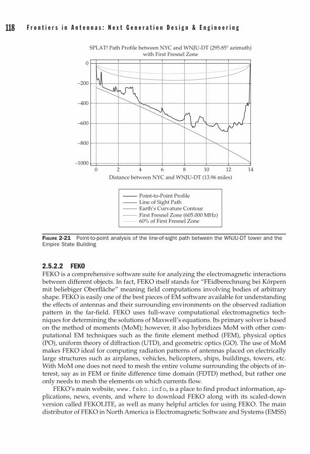
118 F r o n t i e r s i n a n t e n n a s : N e x t G e n e r a t i o n D e s i g n & e n g i n e e r i n g C h a p t e r 2 : S m a r t a n t e n n a s 119
2.5.2.2 FEKOFEKO is a comprehensive software suite for analyzing the electromagnetic interactions between different objects. In fact, FEKO itself stands for “FEidberechnung bei Körpern mit beliebiger Oberfläche” meaning field computations involving bodies of arbitrary shape. FEKO is easily one of the best pieces of EM software available for understanding the effects of antennas and their surrounding environments on the observed radiation pattern in the far-field. FEKO uses full-wave computational electromagnetics tech-niques for determining the solutions of Maxwell’s equations. Its primary solver is based on the method of moments (MoM); however, it also hybridizes MoM with other com-putational EM techniques such as the finite element method (FEM), physical optics (PO), uniform theory of diffraction (UTD), and geometric optics (GO). The use of MoM makes FEKO ideal for computing radiation patterns of antennas placed on electrically large structures such as airplanes, vehicles, helicopters, ships, buildings, towers, etc. With MoM one does not need to mesh the entire volume surrounding the objects of in-terest, say as in FEM or finite difference time domain (FDTD) method, but rather one only needs to mesh the elements on which currents flow.
FEKO’s main website, www.feko.info, is a place to find product information, ap-plications, news, events, and where to download FEKO along with its scaled-down version called FEKOLITE, as well as many helpful articles for using FEKO. The main distributor of FEKO in North America is Electromagnetic Software and Systems (EMSS)
0 2 4 6 8
SPLAT! Path Profile between NYC and WNJU-DT (295.85° azimuth)with First Fresnel Zone
10
Point-to-Point ProfileLine of Sight PathEarth’s Curvature ContourFirst Fresnel Zone (605.000 MHz)60% of First Fresnel Zone
12 14–1000
–800
–600
–400
–200
0
Distance between NYC and WNJU-DT (13.96 miles)
Figure 2-21 Point-to-point analysis of the line-of-sight path between the WNJU-DT tower and the Empire State Building

118 F r o n t i e r s i n a n t e n n a s : N e x t G e n e r a t i o n D e s i g n & e n g i n e e r i n g C h a p t e r 2 : S m a r t a n t e n n a s 119
of Hampton, VA owned and operated by Dr. C.J. Reddy. Their main website is www .emssusa.com. EMSS also serves as the help center for questions about FEKO. FEKO is in widespread use by industry, government, and academia. Recently, the Applied Computational Electromagnetic Society (ACES) added to its yearly conference several special sessions on FEKO and its use. ACES 2008 in Monterey, CA included 6 different sessions and over 30 papers. Additionally, Randy Haupt’s new book Antenna Arrays: A Computational Approach (Wiley, 2010) contains a great deal of simulations performed in FEKO. Private use of FEKO is not widespread due primarily to the licensing structure of FEKO, which makes it unaffordable for individuals. However, FEKO recently unveiled a partnership with a web based-service provider called Crunchyard (www.crunchyard.com), which facilitates pay-per-use simulation of FEKO models on large computer clusters. This may remove the barriers to accessing FEKO for small time users in the future.
FEKO has several modules for designing, analyzing, and visualizing models. The names are CADFEKO, POSTFEKO, OPTFEKO, TIMEFEKO, and EDITFEKO. CAD-FEKO is the primary tool for creating, meshing, and preparing models for simulation. It has several built-in tools for creating primitive shapes such as wires, polygons, spheres, tetrahedron, cylinders, etc. as well as the ability to import CAD models created in AutoCAD, SolidWorks, and other programs.
Figure 2-23 is a screenshot of the CADFEKO environment for FEKO 5.5.POSTFEKO is the primary tool for visualizing the results of simulations. The image
of the radiation pattern on an airplane of Fig. 2-22 was created in POSTFEKO. Figure 2-24 is a screenshot of the POSTFEKO environment for FEKO 5.5. OPTFEKO is an engine for performing optimization of models. Of note is that OPTFEKO incorporates both Genetic Algorithms and Particle Swarm Optimization as primary methods of optimization.
Figure 2-22 Radiation pattern of antenna on airplane and instantaneous current distribution on aircraft skin

120 F r o n t i e r s i n a n t e n n a s : N e x t G e n e r a t i o n D e s i g n & e n g i n e e r i n g C h a p t e r 2 : S m a r t a n t e n n a s 121
In addition, traditional optimization methods such as Simplex (Nelder-Mead) and Grid Search are included.
TIMEFEKO is a tool for performing time-domain analyses in FEKO. Since FEKO is based on MoM, to gather frequency information over a broadband one needs to simu-late multiple frequencies one at a time. This is where a method such as FDTD is pre-ferred. TIMEFEKO performs time-domain analyses by creating time domain pulse shapes and applying Fourier transforms on broadband frequency domain data.
EDITFEKO is the backbone of FEKO and serves as an editor for the solution settings in FEKO before simulating. A screenshot for the EDITFEKO environment is provided in Fig. 2-25. Years ago FEKO only consisted of EDITFEKO. CADFEKO did not exist. One had to enter in commands to create geometries, which could be quite cumbersome. As time progressed, CADFEKO was introduced and many of the capabilities of EDITFEKO have been ported over. However, there are still some advanced features available in EDITFEKO that are not in CADFEKO. The EDITFEKO file with extension .pre can be opened with a simple ASCII text editor. As such, EDITFEKO lends itself quite well to performing optimization of models outside of FEKO’s OPTFEKO environment. The .pre file can be modified external to FEKO from the command-line, MATLAB or any other scripting environment and then commands can be executed to run the FEKO kernel for that given .pre file. This gives the user freedom to mesh a geometry, remesh, manipulate geometries, and change calculations through parameterization of variables in the EDIT-FEKO file. The resulting output files .out, .ffe, or others can be read and information extracted to compute performance of sources, far-fields, near-fields, impedance, VSWR, etc. Internal to EDITFEKO are commands for looping through multiple simulations as well if so desired.
Figure 2-23 Screenshot of CADFEKO environment

120 F r o n t i e r s i n a n t e n n a s : N e x t G e n e r a t i o n D e s i g n & e n g i n e e r i n g C h a p t e r 2 : S m a r t a n t e n n a s 121
2.5.2.3 Numerical Electromagnetics CodeNumerical Electromagnetics Code(NEC) is a computer-based program that computes the electromagnetic response and interaction of antennas and other structures com-posed of metallic wires using the Method of Moments (MoM) computational electro-magnetic technique. It was originally developed by Lawrence Livermore National Laboratory and the University of California in 1981 [54]. The latest variant of the code is called NEC4 and its use is licensed through Lawrence Livermore and is under United States export control. The latest version available in the public domain without requir-ing a license is NEC2. The use of NEC2 in the public domain is extensive and its avail-ability is widespread. The main resources for NEC2 codes are
http://www.nec2.org/http://www.si-list.net/swindex.html#nec2pp The first resource provides links to a theoretical background on the numerical meth-
ods applied in NEC2 as well as descriptions on the program operation and code details. The second resource is considered the “Unofficial NEC Archives” wherein one will find links to different versions of NEC2 code compiled under different operating systems, languages and code. Commercial codes are available for purchase that incorporate NEC2/NEC4 engines. An example of such a product is W7EL’s EZNEC (www.eznec .com). EZNEC is GUI based, therefore it is not conducive to optimization. Here we will focus explicitly on the consolidation of command-line NEC2 within optimization rou-tines for smart antenna applications.
There is nothing new about the use of NEC in the analysis and design of antennas, but oftentimes in literature, particularly for those concerned with array pattern synthe-sis, the effects of mutual coupling between antennas and other objects in the environ-ment are not considered. The results presented may not be physically realizable and
Figure 2-24 Screenshot of POSTFEKO environment

122 F r o n t i e r s i n a n t e n n a s : N e x t G e n e r a t i o n D e s i g n & e n g i n e e r i n g C h a p t e r 2 : S m a r t a n t e n n a s 123
may not be observed when the antenna array is deployed into the real world. With that said, in the absence of access to commercially available codes, public NEC2 codes are perfectly suitable for incorporation into the antenna array design process. A NEC2 model may include lossy conductors, nonradiating networks, transmission lines, lumped elements, transformers, and perfect and imperfect ground planes. More com-plicated antenna elements can be constructed from smaller segments, provided the seg-ment length is small compared to a wavelength.
The appeal of NEC2 is its command-line structure. This makes it ideal for batch processing and incorporation into optimization routines. An excellent example of a marriage between NEC2 code and optimization routines is Derek Linden’s MIT Dis-sertation entitled “Automated Design and Optimization of Wire Antennas Using Ge-netic Algorithms” [55]. Therein, he incorporated NEC2 code driven by a batch process-ing script to genetically optimize the Cartesian coordinates of a wire antenna composed of segments and confined to fit inside a 3D volume. He optimized for antenna pattern shape and polarization. His work resulted in an antenna whose appearance was odd, but had impressive characteristics that could not have been achieved with traditional design methods. The optimization is performed by passing new inputs to a data file, executing the NEC2 code for this input file, reading the outputs, and then adjusting the input file in response to this feedback. This requires the ability to read and write to files as well as loop and replace variables. This can easily be set up in a batch processing script or in a programming environment such as MATLAB.
The general structure of the NEC2 input file is based on the punch card format used by early digital computers; people were actually using punch cards when they developed
Figure 2-25 Screenshot of EDITFEKO environment
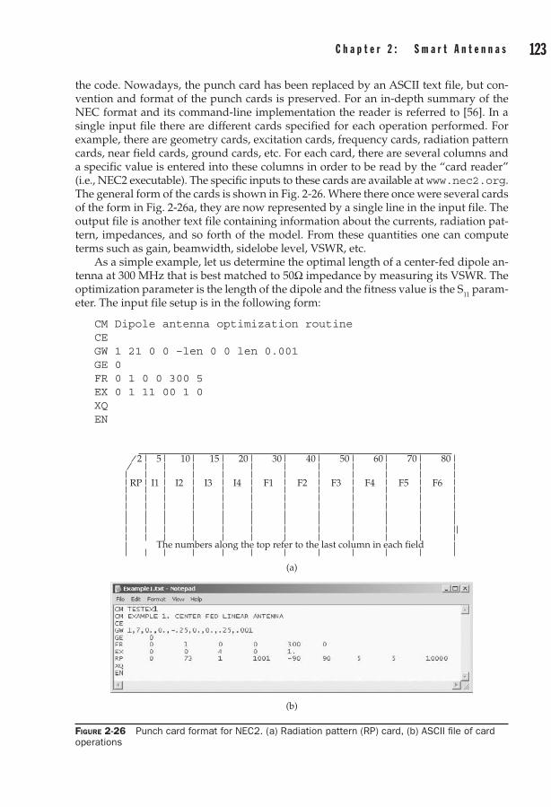
122 F r o n t i e r s i n a n t e n n a s : N e x t G e n e r a t i o n D e s i g n & e n g i n e e r i n g C h a p t e r 2 : S m a r t a n t e n n a s 123
(a)
(b)
RP I1 I2
The numbers along the top refer to the last column in each field
I3 I4 F1 F2 F3 F4 F5 F6
2 5 10 15 20 30 40 50 60 70 80
Figure 2-26 Punch card format for NEC2. (a) Radiation pattern (RP) card, (b) ASCII file of card operations
the code. Nowadays, the punch card has been replaced by an ASCII text file, but con-vention and format of the punch cards is preserved. For an in-depth summary of the NEC format and its command-line implementation the reader is referred to [56]. In a single input file there are different cards specified for each operation performed. For example, there are geometry cards, excitation cards, frequency cards, radiation pattern cards, near field cards, ground cards, etc. For each card, there are several columns and a specific value is entered into these columns in order to be read by the “card reader” (i.e., NEC2 executable). The specific inputs to these cards are available at www.nec2.org. The general form of the cards is shown in Fig. 2-26. Where there once were several cards of the form in Fig. 2-26a, they are now represented by a single line in the input file. The output file is another text file containing information about the currents, radiation pat-tern, impedances, and so forth of the model. From these quantities one can compute terms such as gain, beamwidth, sidelobe level, VSWR, etc.
As a simple example, let us determine the optimal length of a center-fed dipole an-tenna at 300 MHz that is best matched to 50Ω impedance by measuring its VSWR. The optimization parameter is the length of the dipole and the fitness value is the S11 param-eter. The input file setup is in the following form:
CM Dipole antenna optimization routineCEGW 1 21 0 0 –len 0 0 len 0.001GE 0FR 0 1 0 0 300 5EX 0 1 11 00 1 0XQEN

124 F r o n t i e r s i n a n t e n n a s : N e x t G e n e r a t i o n D e s i g n & e n g i n e e r i n g C h a p t e r 2 : S m a r t a n t e n n a s 125
Note that in the GW card the term len is the substitution variable for the length of the dipole. The optimization routine chosen is the Cross Entropy method as discussed previously. The results are shown in Fig. 2-27. The optimal length determined by the routine is just under l/2 with a fitness value or S11 of –15 dB. This matches theory if the source impedance were matched perfectly with the dipole’s impedance.
2.6 ConclusionThis chapter addressed a small subset of all possible frontiers in smart antennas and focused specifically on the two most fundamental components of a smart antenna: (1) adaptive signal processing and (2) direction-of-arrival estimation. The motivation for using stochastic, population-based adaptive processing techniques is their ability to solve complex problems often encountered in smart antenna design. Examples were performed for adaptive beamforming and nulling of interferers by measuring the out-put power of the array. Additionally, some suggestions were offered for improvements to the algorithms to help facilitate their use as adaptive signal processing techniques. This was followed up by a discussion into recent advances in incoherent wideband di-rection-of-arrival estimation, namely those based on tests of orthogonality between sig-nal and noise subspaces. The use of incoherent methods is motivated by the favorable SNR conditions of wireless communications channels compared to their radar counterparts. Finally, knowledge-aided smart antennas were discussed to highlight the wealth of information available for public consumption that the smart antenna designer can incorporate to increase the fidelity of their models. Furthermore, with an increase in computing power more information can be digested quickly allowing algorithms to take into account environmental effects surrounding the smart antenna in order to mit-igate their influence on performance. This discussion is but a small subset of all possible
Figure 2-27 Optimization of a center-fed dipole antenna using NEC2 and optimization routine. Optimal length is computed to be just under λ/2.
End2:(x,y,z) = (0,0,+z/2)
x
y
z
End1:(x,y,z) = (0,0,–z/2)
5 10 15 20 25 30–20
–10
0
No. Iterations
Bes
t & A
vgSc
ore
Best ScoreAvg Score
5 10 15 20 25 300.4
0.5
0.6
0.7
0.8
No. IterationsD
ipol
e L
engt
h of
Bes
t & A
vg S
core Length of Best Score
Length of Avg Score

124 F r o n t i e r s i n a n t e n n a s : N e x t G e n e r a t i o n D e s i g n & e n g i n e e r i n g C h a p t e r 2 : S m a r t a n t e n n a s 125
frontiers in smart antennas, but with the an increase in the demand for mobile commu-nications comes an increase in the number of users, increased data rates and increased bandwidths that smart antenna processing can improve and increase, and must ac-count for.
AcknowledgmentsThe author would like to acknowledge his colleagues at ArgonST, specifically Skip Gross, Robert Kellogg and Nathan Brooks for their many discussions on the topic, sup-port throughout the writing process, and input on editing.
ReferencesJ. Dong, A. I. Zaghloul, R. Sun, C. J. Perry, and S. J. Weiss, “Rotman lens amplitude, phase and [1] pattern evaluations by measurements and full-wave simulations,” ACES Journal, vol. 24, no.6, pp. 567–576, Dec. 2009. B. Widrow, P. Mantey, L. Griffiths, et al., “Adaptive Antenna Systems,” [2] Proc. IEEE, vol. 55, Dec. 1967.F. B. Gross, [3] Smart Antennas for Wireless Communications with MATLAB. McGraw-Hill, 2005.R. L. Kellogg, E. Mack and C. Crews, “Direction Finding Antennas and Systems,” [4] Antenna Engineering Handbook, Ch. 47. M. Pesavento, A. B. Gershman, and K. M. Wong, “Direction finding using partly calibrated sensor [5] arrays comprised of multiple subarrays,” IEEE Trans. Signal Process, 50 (9), pp. 2103–2115. F. Gao, and A. B. Gershman, “A generalized ESPRIT approach to direction-of-arrival estimation,” [6] IEEE Signal Process. Lett., 12 (3), pp. 254–257.M. Rubsamen, and A. B. Gershmann, “Direction of arrival estimation for non-uniform sensor arrays: [7] From manifold separation to Fourier Domain MUSIC methods,” IEEE Trans. Signal Process., 57 (2), pp. 588–599. K. Guney, and S. Basbug, “Interference suppression of linear antenna arrays by amplitude-only [8] control using a bacterial foraging algorithm,” Progress in Electromagnetics Research, PIER 79, pp. 475–497, 2008.R. L. Haupt, and D. H. Werner, [9] Genetic Algorithms in Electromagnetics, New York: Wiley-Interscience, 2007.R. L. Haupt, “Antenna Design with a Mixed Integer Genetic Algorithm,” [10] IEEE Trans. on Ant. and Propagat. vol. 55, no. 3, pp. 577–582, Mar. 2007.K. A. De Jong, [11] Analysis of the Behavior of a Class of Genetic Adaptive Systems, PhD Dissertation, Univ. of Michigan-Ann Arbor, 1975.J. J. Grefenstette, “Optimization of control parameters for genetic algorithms,” [12] IEEE Trans. Syst. Man. Cybern. SMC 16: 128, Jan/Feb 1986.J. Kennedy, and R. C. Eberhart, [13] Swarm Intelligence. San Francisco: Morgan Kauffman Publishers, 2001.T. M. Cover, and J. A. Thomas, [14] Elements of Information Theory. New York: Wiley, 1991.J. N. Kapur, and H. K. Kesavan, [15] Entropy Optimization Principles with Applications. New York: Academic Press, 1992.R. Y. Rubinstein, “Optimization of Computer Simulation Models with Rare Events,” [16] European Journal of Operational Research, vol. 99, pp. 89–112, 1997.R. Y. Rubinstein, “The Cross Entropy Method for Combinatorial and Continuous Optimization,” [17] Methodology and Computing in Applied Probability, vol. 1, Jan. pp. 127–190, 1999.J. D. Connor, [18] Antenna Array Synthesis Using the Cross Entropy Method. PhD Dissertation, Florida State University, 2008. J. D. Connor, S. Y. Foo, and M. H. Weatherspoon, “Synthesizing Antenna Array Sidelobe Levels and [19] Null Placements Using the Cross Entropy Method,” Proceedings of the 2008 IEEE Industrial Electronics Conference, Orlando, pp. 1937–1941, 2008. J. Liu, “Global Optimization Techniques Using Cross Entropy and Evolution Algorithms,” Master’s [20] Thesis, Department of Mathematics, The University of Queensland, 2004.P. T. de Boer, “Analysis and Efficient Simulation of Queuing Models of Telecommunications [21] Systems,” PhD Dissertation, University of Twente, 2000.J. Keith, and D. P. Kroese, “Sequence Alignment by Rare Event Simulation,” [22] Proceedings of the 2002 Winter Simulation Conference, San Diego, pp. 320—327, 2002.

126 F r o n t i e r s i n a n t e n n a s : N e x t G e n e r a t i o n D e s i g n & e n g i n e e r i n g
L. Margolin, “Cross Entropy Method for Combinatorial Optimization,” Master’s Thesis, The [23] Technion, Israel Institute of Technology, Haifa, July 2002. K. Chepuri, and T. Homem de Mello, “Solving the Vehicle Routing Problem with Stochastic [24] Demands Using Cross Entropy Method,” Annals of Operations Research, Kluwer Academic, 2004.I. Szita and A. Lorincz, “Learning Tetris Using the Noisy Cross Entropy Method,” [25] Neural Computation, vol. 18, no. 12, pp. 2936–2941, Dec. 2006.Y. Chen, and Y. T. Su, “Maximum Likelihood DOA Estimation Based on the Cross Entropy Method,” [26] Information Theory, 2006 IEEE International Symposium, pp. 851–855, July 2006.M. Joost, and W. Schiffmann, “Speeding Up Backpropagation Algorithms by Using Cross Entropy [27] Combined with Pattern Normalization,” International Journal of Uncertainty, Fuzziness and Knowledge-based Systems, 1997. M. Dorigo, M. Zlochin, N. Meuleau, and M. Birattari, “Updating ACO Pheromones Using Stochastic [28] Gradient Ascent and Cross Entropy Methods,” Applications of Evolutionary Computing in vol. 2279 of Lecture Notes in Computer Science, pp. 21–30, 2002. Z. Liu, A. Doucet, and S. Singh, “The Cross Entropy Method for Blind Multi-user Detection,” [29] Information Theory, 2004 ISIT 2004, Proceedings, International Symposium pp. 510, July 2004.Y. Zhang, et al., “Cross Entropy Optimization of Multiple-Input Multiple-Output Capacity by [30] Transmit Antenna Selection,” IET Microwaves, Antennas & Propagation. vol. 1, no. 6, pp. 1131–1136, Dec. 2007.http://iew3.technion.ac.il/CE/pubs.php [31] R. Y. Rubinstein, and D. P. Kroese, [32] The Cross-Entropy Method: A Unified Approach to Combinatorial Optimization, Monte-Carlo Simulation and Machine Learning. New York: Springer, 2004.P. Boer, D. Kroese, S. Manor, and R. Rubinstein. “A tutorial on the cross-entropy method,” http://[33] iew3.technion.ac.il/CE/tutor.php, 2002.http://iew3.technion.ac.il/CE/ (formerly www.cemethod.org)[34] http://www.maths.uq.edu.au/CEToolBox/[35] A. Costs, O. D. Jones, and D. P. Kroese, “Convergence Properties of the Cross-Entropy Method for [36] Discrete Optimization,” Operations Research Letters, vol. 35, no. 5, pp. 573–580, Sept. 2007.R. L. Haupt, “Phase-only adaptive nulling with a genetic algorithm”, [37] IEEE Trans. on Ant. and Propagat., vol. 45, no. 6, pp. 1009–1015, Jun. 1997.R. A. Shore, “A proof of the odd-symmetry of the phase for minimum weight perturbation phase-[38] only null synthesis,” IEEE Trans. Ant. and Propagat., vol. AP-32, pp. 528–530, May 1984.M. Wagih, and H. M. Elkamchouchi, “Application of particle swarm optimization algorithm in [39] smart antenna array systems,” http://intechweb.org/downloadpdf.php?id=6279.Z. Botev, and D. P. Kroese. “Global Likelihood Optimization via the Cross-Entropy Method with [40] an Application to Mixture Models,” IEEE Proceedings of the 2004 Winter Simulation Conference, vol. 1. Dec. 2004.S. Y. Yoon, “Direction-of-arrival estimation of wideband sources using sensor arrays,” PhD [41] Dissertation, Georgia Institute of Technology, 2004. K. Okane, S. Ikeda, and T. Ohtsuki, “Improvement of estimation accuracy of wideband DOA esti-[42] mation “TOPS”,” 2009 Annual Summit and Conference of Asia-Pacific Signal and Information Processing Assocation (SPSIPA ASC 2009), Oct. 2009. H. Yu, J. Liu, Z. Huang, Y. Zhou, and X. Xu, “A new method for wideband DOA estimation,” [43] IEEE WICOM 2007, Int. Conf. on Wireless Comm., Networking and Mobile Computing, pp. 598–601, Sept. 2007. L. Margolin, “On the Convergence of the Cross-Entropy Method,” [44] Annals of Operations Research, vol. 134, pp. 201–214, 2004.http://www.darpa.mil/STO/space/kassper.html[45] http://www.darpa.mil/STO/space/mer.html[46] http://geoengine.nga.mil/muse-cgi-bin/rast_roam.cgi[47] http://www2.jpl.nasa.gov/srtm[48] http://www.qsl.net/kd2bd/splat.html[49] http://flattop.its.bldrdoc.gov/itm.html [50] http://www.gnu.org/licenses/gpl.html[51] www.gnuplot.info[52] http://www.ieee.org/organizations/society/bt/newletterbkissues.html[53] G. J. Burke, and A. J. Poggio, “Numerical Electromagnetics Code (NEC)—Method of Moments,” [54] NOSC TD 116, Jan. 1981.D. S. Linden, “Automated Design and Optimization of Wire Antennas Using Genetic Algorithms,” [55] PhD Dissertation, Massachusetts Institute of Technology, 1997. D. B. Miron, [56] Small Antenna Design, Chs. 4–5. Elsevier, 2006.
Chapter 3Vivaldi antenna arrays
Marinos N. Vouvakis and Daniel h. Schaubert
3.1 Background and General Characteristics
3.1.1 IntroductionVivaldi antenna arrays were first demonstrated in the 1970s, but their development and use in systems required many years. The operation of Vivaldi arrays, like all phased arrays, strongly depends on coupling between the array elements. Successful wideband Vivaldi array designs require accurate full-wave simulation to characterize these coupling effects and to adjust the element and array design to achieve good impedance match over wide frequency bands and wide ranges of scan angle. When Lewis, Fassett, and Hunt [1] first demonstrated a Vivaldi array in 1974, desktop computers and full-wave computational electromagnetic (CEM) simulators were not powerful enough to analyze three-dimensional Vivaldi arrays. Over the next 15 years, computers and algorithms improved so that unit cell analysis of infinite arrays could be performed in a few hours, permitting accurate prediction of array performance, and subsequently leading to wider bandwidth array designs with good scan performance.
Vivaldi arrays can now be designed to operate over greater than 10:1 bandwidth. Although there are other wideband array configurations, the Vivaldi array has been used more extensively and has become the standard to which wide bandwidth array performance is compared.
As of this time, no competing array technology can match the wide bandwidth and wide scanning impedance performance of Vivaldi arrays, particularly when practical constraints such as minimizing element count (i.e., requiring element spacing to be as close as possible to l/2 at the highest frequency) are imposed. However, Vivaldi arrays produce higher levels of cross polarization than some other arrays when scanned in the intercardinal planes.
Wide bandwidth performance is achieved only when the Vivaldi elements are elec-trically connected to their neighbors. This creates troublesome manufacturing prob-lems for dual-polarized Vivaldi arrays. Vivaldi arrays require slightly more depth than some of the competing array configurations [2]–[7], but they do not require special dielectric properties that are sometimes used for these alternative configurations. Unlike many of the dipole-like array elements, Vivaldi antennas include a transition
127

128 F r o n t i e r s i n a n t e n n a s : N e x t G e n e r a t i o n D e s i g n & e n g i n e e r i n g C h a p t e r 3 : V i v a l d i a n t e n n a a r r a y s 129
from stripline or microstrip to slotline that acts as an internal balun; therefore, no external balun is required for wide bandwidth operation.
This chapter presents performance studies of Vivaldi arrays that operate up to 10:1 bandwidth. Studies of a canonical, infinite array show how key design parameters affect array performance, providing guidance to initiate and optimize the design of such an array. Also, simulations of finite Vivaldi arrays using the Domain Decomposition-Finite Element Method (DD-FEM) are presented. These simulations show the truncation effects that are observed when these arrays are not extremely large and also illustrate the capabilities of DD-FEM, which is a powerful simulation tool for array design and evaluation.
3.1.2 BackgroundThe use of stripline-fed notch antennas as elements for wide bandwidth arrays was demonstrated by Lewis, Fassett, and Hunt in 1974 [1], where the gain of an 8 × 8 array over 5:1 bandwidth was presented. The array gain for a broadside beam increases approximately as the square of the frequency, as expected for a fixed aperture size. Their results show no serious resonances to disrupt array performance, even though the element spacing is 0.953l at the highest frequency, which now is known to produce several resonances in the upper portion of the frequency range if the array has a large number of elements. They also show array gain vs. frequency for several E-plane scan angles over slightly more than one octave of bandwidth. The E-plane gain shows a dip near midband that is probably associated with a resonance. Nevertheless, this pio-neering work motivated the development of wide bandwidth notch arrays.
In 1979, Gibson presented a paper showing a single end-fire tapered slot antenna with exponential flare, which he called the “Vivaldi” aerial [8]. Gibson’s designation has since become associated with this type of antenna element and with arrays of the elements.
During the 1980s, many groups studied wide bandwidth Vivaldi-like arrays. Proto-type arrays were demonstrated, for example in [9]. Numerous resonances or imped-ance anomalies were observed, and some of these were corrected by adjusting the element design and/or spacing in the array.
By the early 1990s desktop computing was becoming powerful enough to analyze infinite arrays of Vivaldi antennas using the unit cell approach [10]–[13]. Embedded element patterns of a dual-polarized 1799-element array showed excellent perfor-mance over a 3:1 bandwidth [14]. Throughout the 1990s, computer power increased and CEM algorithms improved so that studies could be completed to evaluate the effects of several design parameters on array performance [15], [16]. By 1999, Vivaldi arrays could be designed using these parameter studies and infinite array analysis. Arrays were designed to operate over multiple octaves of bandwidth, scanning to 45° or more, with VSWR<2 and no anomalous impedance behavior.
In 2001, Schuneman, et al., [17] reported an array design with 10:1 bandwidth. Over the following years, several Vivaldi arrays were designed to operate over bandwidths of a decade or more. By 2008, experienced array designers with a laptop computer and one of several commercial electromagnetic analysis codes could design a Vivaldi array with decade bandwidth and good scanning performance.
3.1.3 ApplicationsOver the years, Vivaldi antenna arrays have become the aperture of choice for many applications that require bandwidths upward of 4:1 and wide-angle scanning. Vivaldi apertures are often used in military applications including electronic warfare (EW)
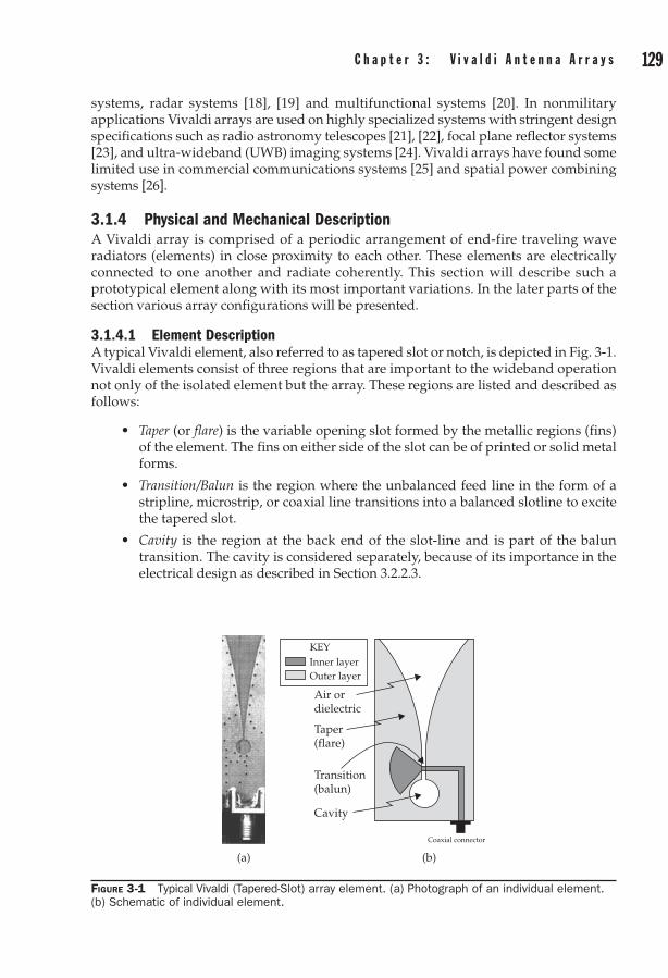
128 F r o n t i e r s i n a n t e n n a s : N e x t G e n e r a t i o n D e s i g n & e n g i n e e r i n g C h a p t e r 3 : V i v a l d i a n t e n n a a r r a y s 129
systems, radar systems [18], [19] and multifunctional systems [20]. In nonmilitary applications Vivaldi arrays are used on highly specialized systems with stringent design specifications such as radio astronomy telescopes [21], [22], focal plane reflector systems [23], and ultra-wideband (UWB) imaging systems [24]. Vivaldi arrays have found some limited use in commercial communications systems [25] and spatial power combining systems [26].
3.1.4 Physical and Mechanical DescriptionA Vivaldi array is comprised of a periodic arrangement of end-fire traveling wave radiators (elements) in close proximity to each other. These elements are electrically connected to one another and radiate coherently. This section will describe such a prototypical element along with its most important variations. In the later parts of the section various array configurations will be presented.
3.1.4.1 Element DescriptionA typical Vivaldi element, also referred to as tapered slot or notch, is depicted in Fig. 3-1. Vivaldi elements consist of three regions that are important to the wideband operation not only of the isolated element but the array. These regions are listed and described as follows:
Taper • (or flare) is the variable opening slot formed by the metallic regions (fins) of the element. The fins on either side of the slot can be of printed or solid metal forms.
Transition/Balun • is the region where the unbalanced feed line in the form of a stripline, microstrip, or coaxial line transitions into a balanced slotline to excite the tapered slot.
Cavity • is the region at the back end of the slot-line and is part of the balun transition. The cavity is considered separately, because of its importance in the electrical design as described in Section 3.2.2.3.
Figure 3-1 Typical Vivaldi (Tapered-Slot) array element. (a) Photograph of an individual element. (b) Schematic of individual element.
(a) (b)
Coaxial connector
Cavity
Transition(balun)
Taper(flare)
Inner layerOuter layer
Air ordielectric
KEY
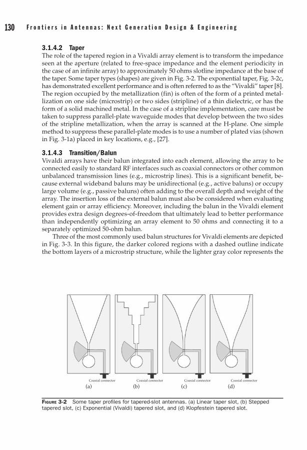
130 F r o n t i e r s i n a n t e n n a s : N e x t G e n e r a t i o n D e s i g n & e n g i n e e r i n g C h a p t e r 3 : V i v a l d i a n t e n n a a r r a y s 131
3.1.4.2 TaperThe role of the tapered region in a Vivaldi array element is to transform the impedance seen at the aperture (related to free-space impedance and the element periodicity in the case of an infinite array) to approximately 50 ohms slotline impedance at the base of the taper. Some taper types (shapes) are given in Fig. 3-2. The exponential taper, Fig. 3-2c, has demonstrated excellent performance and is often referred to as the “Vivaldi” taper [8]. The region occupied by the metallization (fin) is often of the form of a printed metal-lization on one side (microstrip) or two sides (stripline) of a thin dielectric, or has the form of a solid machined metal. In the case of a stripline implementation, care must be taken to suppress parallel-plate waveguide modes that develop between the two sides of the stripline metallization, when the array is scanned at the H-plane. One simple method to suppress these parallel-plate modes is to use a number of plated vias (shown in Fig. 3-1a) placed in key locations, e.g., [27].
3.1.4.3 Transition/BalunVivaldi arrays have their balun integrated into each element, allowing the array to be connected easily to standard RF interfaces such as coaxial connectors or other common unbalanced transmission lines (e.g., microstrip lines). This is a significant benefit, be-cause external wideband baluns may be unidirectional (e.g., active baluns) or occupy large volume (e.g., passive baluns) often adding to the overall depth and weight of the array. The insertion loss of the external balun must also be considered when evaluating element gain or array efficiency. Moreover, including the balun in the Vivaldi element provides extra design degrees-of-freedom that ultimately lead to better performance than independently optimizing an array element to 50 ohms and connecting it to a separately optimized 50-ohm balun.
Three of the most commonly used balun structures for Vivaldi elements are depicted in Fig. 3-3. In this figure, the darker colored regions with a dashed outline indicate the bottom layers of a microstrip structure, while the lighter gray color represents the
Figure 3-2 Some taper profiles for tapered-slot antennas. (a) Linear taper slot, (b) Stepped tapered slot, (c) Exponential (Vivaldi) tapered slot, and (d) Klopfestein tapered slot.
(a) (b) (c) (d)Coaxial connector Coaxial connector Coaxial connector Coaxial connector
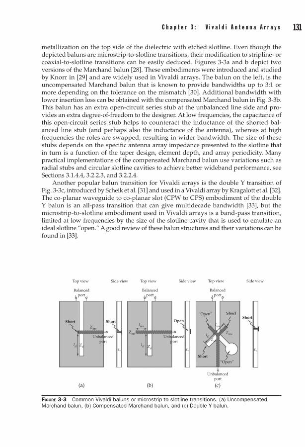
130 F r o n t i e r s i n a n t e n n a s : N e x t G e n e r a t i o n D e s i g n & e n g i n e e r i n g C h a p t e r 3 : V i v a l d i a n t e n n a a r r a y s 131
metallization on the top side of the dielectric with etched slotline. Even though the depicted baluns are microstrip-to-slotline transitions, their modification to stripline- or coaxial-to-slotline transitions can be easily deduced. Figures 3-3a and b depict two versions of the Marchand balun [28]. These embodiments were introduced and studied by Knorr in [29] and are widely used in Vivaldi arrays. The balun on the left, is the uncompensated Marchand balun that is known to provide bandwidths up to 3:1 or more depending on the tolerance on the mismatch [30]. Additional bandwidth with lower insertion loss can be obtained with the compensated Marchand balun in Fig. 3-3b. This balun has an extra open-circuit series stub at the unbalanced line side and pro-vides an extra degree-of-freedom to the designer. At low frequencies, the capacitance of this open-circuit series stub helps to counteract the inductance of the shorted bal-anced line stub (and perhaps also the inductance of the antenna), whereas at high frequencies the roles are swapped, resulting in wider bandwidth. The size of these stubs depends on the specific antenna array impedance presented to the slotline that in turn is a function of the taper design, element depth, and array periodicity. Many practical implementations of the compensated Marchand balun use variations such as radial stubs and circular slotline cavities to achieve better wideband performance, see Sections 3.1.4.4, 3.2.2.3, and 3.2.2.4.
Another popular balun transition for Vivaldi arrays is the double Y transition of Fig. 3-3c, introduced by Scheik et al. [31] and used in a Vivaldi array by Kragalott et al. [32]. The co-planar waveguide to co-planar slot (CPW to CPS) embodiment of the double Y balun is an all-pass transition that can give multidecade bandwidth [33], but the microstrip-to-slotline embodiment used in Vivaldi arrays is a band-pass transition, limited at low frequencies by the size of the slotline cavity that is used to emulate an ideal slotline “open.” A good review of these balun structures and their variations can be found in [33].
Figure 3-3 Common Vivaldi baluns or microstrip to slotline transitions. (a) Uncompensated Marchand balun, (b) Compensated Marchand balun, and (c) Double Y balun.
Short
Balancedport+ – + – + –
Balancedport
Balancedport
(a) (b) (c)
Side viewTop viewSide viewTop viewSide viewTop view
Short
Short
Short
ShortOpen
“Open”
“Open”
Unbalancedport
ZmsZms Zms
Zsl Zslεr εr εr
lsl lsl
lsl
lms lms
Unbalancedport
Unbalancedport
Zsl

132 F r o n t i e r s i n a n t e n n a s : N e x t G e n e r a t i o n D e s i g n & e n g i n e e r i n g C h a p t e r 3 : V i v a l d i a n t e n n a a r r a y s 133
3.1.4.4 CavityThe cavity at the bottom of the taper is part of the balun transition and affects the antenna array matching. Some variations of the slot cavity are shown in Fig. 3-4. As noted in the transition/balun section, the cavity should provide large inductive reac-tance at low frequencies. This can best be achieved by increasing the characteristic impedance of the slotline, often achieved by increasing the slot width, Fig. 3-4b. As is visible from Fig. 3-4b, a rectangular cavity could partially overlap the radial stub, eliminating a portion of its ground plane. The circular cavity in Fig. 3-4c provides the required reactance to the slotline junction and also maintains the ground plane for the radial stub feed line. This design allows for more stub space, and favors microstrip-line circular bends (cf. Fig. 3-16) rather that the right-angle microstrip-line bend illustrated in Fig. 3-4.
3.1.4.5 Array ConfigurationsVivaldi arrays consist of vertically oriented Vivaldi elements that are laterally arranged in a rectangular, hexagonal, or triangular periodic grid. For scanning applications the grid periodicity is set to approximately one-half free-space wavelength at the highest frequency to avoid grading lobes in the band of operation. Vivaldi arrays can be designed and fabricated in single- and dual-polarized configurations, with the latter being most popular because it offers polarization diversity. Single-polarized arrays are easier and cheaper to construct by simply arranging rows of parallel PCB cards. Single-polarized arrays are usually arranged in rectangular grids, while some hexagonal grid arrangements as shown in Fig. 3-5a have been recently documented [34], [35].
The more interesting case of dual-polarized arrays comes in a variety of forms as summarized in Fig. 3-5b–e. By far the most common and thoroughly studied dual-polarized arrangement is that of offset orthogonally oriented elements placed on a square grid, as shown Fig. 3-5b. This configuration is often referred to as egg crate, and is known for its excellent impedance performance at wide bandwidths. When electrically
Figure 3-4 Some cavity (slotline stub on Marchand balun) variations for a Vivaldi element. (a) Low impedance slot-line stub, (b) Rectangular cavity (high-impedance slotline stub), and (c) Circular cavity.
(a) (b) (c)Coaxial connector Coaxial connector Coaxial connector
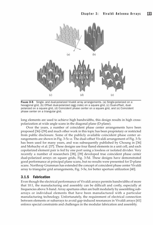
132 F r o n t i e r s i n a n t e n n a s : N e x t G e n e r a t i o n D e s i g n & e n g i n e e r i n g C h a p t e r 3 : V i v a l d i a n t e n n a a r r a y s 133
long elements are used to achieve high bandwidths, this design results in high cross-polarization at wide angle scans in the diagonal plane (D-plane).
Over the years, a number of coincident phase center arrangements have been proposed [36]–[39] and much other work in this topic has been proprietary or restricted from public disclosure. Some of the publicly available coincident phase center ar-rangements are shown in Fig. 3-5c–e. The dual-offset Vivaldi arrangement of Fig. 3-5c has been used for many years, and was subsequently published by Choung in [36] and Mohuchy et al. [37]. These designs use four flared elements in a unit cell, and each copolarized element pair is fed by one port using a lossless or isolated divider. Very recently a number of researchers [38], [39] developed true coincident phase center dual-polarized arrays on square grids, Fig. 3-5d. These designs have demonstrated good performance at principal plane scans, but no results were presented for D-plane scans. Northrop Grumman has extended the concept of coincident phase center Vivaldi array to triangular grid arrangements, Fig. 3-5e, for better aperture utilization [40].
3.1.5 FabricationEven though the electrical performance of Vivaldi arrays permits bandwidths of more that 10:1, the manufacturing and assembly can be difficult and costly, especially at frequencies above X-band. Array apertures often are built modularly by assembling sub-arrays or individual elements that have been manufactured with a particular manufacturing technology. Unfortunately, the requirement of electrical connection between elements or subarrays to avoid gap-induced resonances in Vivaldi arrays [41] enforce special constraints and challenges in the modular fabrication and assembly.
Figure 3-5 Single- and dual-polarized Vivaldi array arrangements. (a) Single-polarized on a hexagonal grid, (b) Offset dual-polarized (egg crate) on a square grid, (c) Dual-offset, dual-polarized on a square grid, (d) Coincident phase center on a square grid, and (e) Coincident phase center on a triangular grid.
(a) (b)
(c) (d) (e)

134 F r o n t i e r s i n a n t e n n a s : N e x t G e n e r a t i o n D e s i g n & e n g i n e e r i n g C h a p t e r 3 : V i v a l d i a n t e n n a a r r a y s 135
3.1.5.1 Manufacturing TechnologiesThere are three popular manufacturing technologies for Vivaldi elements, subarrays, or arrays based on:
• Printedcircuitboard(PCB).In this technology elements or subarrays are formed on stripline or microstrip-line cards using standard high quality microwave laminates, Fig. 3-6a. When fabricating these cards, special care must be taken to chose the subarray size to avoid card bending due to thermal expansion. Such technologies have been used up to 30 GHz. For better tolerances at higher frequencies, photolithographic technologies on hard substrates such as SU-8, SiO2, hi-resistivity Si, and GaAs can be used. Design on such high dielectric constant materials requires special care as described in Section 3.2.2.5.
• 3Dsolidmetal.In this technology elements, subarrays, or arrays are formed from a solid metal block using mechanical mills, wire electric discharge milling (EDM), or laser cutting. When the array is formed out of a solid metal block, electrical connection between elements is ensured. All-metal Vivaldi array designs have good power handling capabilities, but require care to avoid dielectric breakdown at sharp edges and small air gaps. All-metal manufacturing complicates the design and manufacturing of the feed network and balun section. A simple solution was proposed in [42]–[44], where press-on coaxial assemblies are fitted to the back side of the array. This technique requires the modification of the standard flare shape as shown in Fig. 3-6b. Another important example in this category is the body-of-revolution (BOR) Vivaldi array proposed in [45]. An alterative technology to create 3D solid metal designs is to use electroplated molded plastic. This approach has certain weight advantages.
• Hybrid PCB and 3D solid metal. This technology attempts to combine the advantages of each of the above methods, namely the ease of fabrication of the feed network using PCB, and the element-to-element connectivity and power handling of the metallic flares using solid machining. An important example of hybrid manufacturing technologies is Northrop Grumman’s Mecha-notch Vivaldi array shown in Fig. 3-6c, [46]. This technology uses a solid metal flare that is machined with a pocket (cavity) at the base of each element. This pocket is used to house a single metallization layer PCB that hosts the feedline and the stripline stub.
3.1.5.2 Array Assembly (Integration) TechnologiesLarge arrays are seldom built in one piece due to high manufacturing/installation costs and structural and maintenance considerations. Therefore, subarray or ele-ment modularity is a desired feature. Unfortunately, Vivaldi arrays require electri-cal connection among elements and subarrays to avoid gap-induced impedance anom-alies within the bandwidth [41]. This constraint does not pose a major problem in the manufacturing of single-polarized arrays, but it is a major hurdle in the integration of dual-polarized arrays. There are three popular integration technologies for dual- polarized arrays.
1. Vertically integrated PCB cards
2. Puzzle-like integration of solid metal subarray modules
3. Modular fin attachment into a continuous metal base

134 F r o n t i e r s i n a n t e n n a s : N e x t G e n e r a t i o n D e s i g n & e n g i n e e r i n g C h a p t e r 3 : V i v a l d i a n t e n n a a r r a y s 135
In the vertically integrated PCB cards approach, shown in Fig. 3-6a, two sets of orthogonal PCB cards are interleaved to form the egg crate arrangement. The cards use appropriate slots at the places where they meet to facilitate the integration. Maintaining electrical connection at the locations where the two fins from orthogonal polarizations meet poses a major challenge because these regions must be explicitly connected using solder, conductive epoxy, brackets, or other means to eliminate the gap-induced resonances. Given the depth and shape of the egg crate, these connections are tedious and problematic, especially at high frequencies.
In the puzzle-like integration method, solid metal subarray modules (cf. Fig. 3-6b) are placed side-by-side to form a large continuous aperture. This technique tends to work well because the integration is based on subarrays and the possible gaps appear less often than the element-by-element integration. In these designs, subarray electri-cal connection can be achieved with spring-loaded spacers or metallic posts.
Finally, several Vivaldi arrays have been designed using the third integration technique. Due to the topology of the egg crate, every four half-fins meet at a cross point, and they are connected to their opposite side fins only at the base. In this inte-gration technology, this feature is exploited and the four half-fins are machined or cast of solid metal or metalized plastic, and then are modularly attached to a solid back plate that contains the cavity and the feed lines, as shown in Fig. 3-6c. It is noted that electri-cal connection between the fin module and back plate is required, but it can be achieved using screws, solder, epoxy, or a press-fit attachment. The BOR Vivaldi [45] and the work of Trott et al. [38] are two examples of this technology.
Figure 3-6 Vivaldi arrays showing some of the manufacturing and assembly technologies for dual-polarized Vivaldi arrays. (a) Vertically integrated PCB technology (Photograph courtesy of University of Massachusetts). (b) 3D solid aluminum block (Photograph courtesy of Dr. R. Kindt at the Naval Research Lab). (c) Hybrid PCB and metal, Mecha-notch designs (Photograph courtesy of Northrop Grumman).
(c)
(a) (b)

136 F r o n t i e r s i n a n t e n n a s : N e x t G e n e r a t i o n D e s i g n & e n g i n e e r i n g C h a p t e r 3 : V i v a l d i a n t e n n a a r r a y s 137
Figure 3-7 Active reflection coefficient for an isolated Vivaldi element and the respective infinite array. Both configurations are dual-polarized. This element design was optimized to operate in infinite array environment with mutual coupling.
(a)
01 2 5 63 4
Frequency [GHz]
0.2
0.4
|Γ|
0.6
0.8
1Isolated elementInfinite array
3.1.6 General Discussion of Vivaldi Array PerformanceThe radiation performance of a Vivaldi array can be characterized by its impedance and radiation pattern. These figures of merit strongly depend on the mutual coupling between neighboring elements in an array, so a short discussion about the mutual coupling is included.
3.1.6.1 ImpedanceThe impedance behavior of a Vivaldi array is dictated by the element design and by array periodicity, arrangement, and size. When a Vivaldi array has many elements and is electrically large, strong mutual coupling is the dominant factor affecting operation. To demonstrate this, the active reflection coefficient of an infinite, dual-polarized Vivaldi array is plotted in Fig. 3-7, (dashed line) along with the active reflection coefficient of the respective element in isolation (solid line). The two results are quite different, espe-cially at the low end of the frequency band, because of the high mutual coupling between neighboring elements in the array environment. As will be shown in the next section, the mutual coupling in Vivaldi arrays is quite large even between far-separated elements, and is the key for achieving wide bandwidth.
3.1.6.2 Element-to-Element Mutual CouplingTo show the importance of mutual coupling in the active reflection coefficient of Vivaldi arrays, the active reflection coefficient of element mn in a rectangular grid array is expressed as
Γmnp
M
mn pqj p m kd u j q ns e ex( , ) ,( ) ( )θ φ0 0
1
≈=
- - - -∑ 0kkd v
q
Ny 0
=∑
1
where smn,pq is the coupling coefficient (s-parameter) between elements mn and pq, u0 = sinq 0cosf0 and v0 = sinq 0sinf0 are the u-v coordinates at array scan angles q 0 and f0, and

136 F r o n t i e r s i n a n t e n n a s : N e x t G e n e r a t i o n D e s i g n & e n g i n e e r i n g C h a p t e r 3 : V i v a l d i a n t e n n a a r r a y s 137
M, N and dx, dy are the array size and periodicity at x and y directions, respectively. In the above, it is assumed that element mn is located at x = mdx, y = ndy. This expression is exact for single-mode operation that is accurate for large arrays, but approximate for small arrays [47]. Therefore, large coupling significantly affects the active reflection coef-ficient and impedance of the array. To demonstrate the large coupling in Vivaldi arrays, a dual-polarized 17 × 16 × 2 array is simulated using the full-wave domain decomposi-tion finite element methods (DD-FEM). Figures 3-8a and b show the resulting co- and cross-polarized element coupling |si,j| distribution between the center element and the rest of the array elements, at mid-frequency (3.5 GHz). The majority of neighboring elements experience high coupling, ranging from -10 dB to -30 dB, indicating a strong dependence of the active impedance on mutual coupling. Both co- and cross-polarized element couplings are strong, and the stronger coupling occurs between elements in the diagonal directions. Coupling levels tend to increase as the frequency decreases.
3.1.6.3 Far-Field Radiation PatternsBecause Vivaldi arrays operate over large bandwidth, the radiation pattern (especially beamwidth) can change dramatically from lower frequencies to upper frequencies. For example, an array with 16 dual-polarized elements in each direction that is designed for 1–5 GHz will be 8 wavelengths in size at the highest frequency (16 elements spaced at l/2). This can produce broadside beamwidth of approximately 7°. However, the array size is only 1.6 wavelengths at the lowest frequency, producing approximately 35° beamwidth.
The far-field radiation pattern of a 17 × 16 × 2 dual-polarized Vivaldi array, uni-formly excited and scanned at 30° in the H-plane around midband (4 GHz) is plotted in Fig. 3-9. The figure depicts the actual finite array radiation patterns with a solid line, and with a dashed line for the far-field obtained from the same finite array when the infinite array (Floquet) currents are used for the far-field computation. At the forward hemisphere the latter pattern is approximately the same as the pattern obtained through
Figure 3-8 Port coupling distribution across 17 × 16 × 2 dual-polarized Vivaldi array at mid-band frequency when only the middle vertically polarized element in the array is excited and all other ports are terminated. (a) Copolarization port coupling. (b) Cross-polarization port coupling.
1615
13121110987654321
14
Elem
ent i
ndex
17
1516
13121110987654321
14
Elem
ent i
ndex
21 3 4 5 6 7 8 9 10 11 12 13 14 15 16 17Element index
(a)
21 3 4 5 6 7 8 9 10 11 12 13 14 15 16Element index
(b)
–10
–15
–20
–25
–30
–35
–40
–45
–50
–55
–60
–10
–15
–20
–25
–30
–35
–40
–45
–50
–55
–60
5:1 Vivaldi array, simulated co-polcoupling, frequency = 3.5 GHz
5:1 Vivaldi array, simulated cross-polcoupling, frequency = 3.5 GHz

138 F r o n t i e r s i n a n t e n n a s : N e x t G e n e r a t i o n D e s i g n & e n g i n e e r i n g C h a p t e r 3 : V i v a l d i a n t e n n a a r r a y s 139
the classical pattern multiplication of the array factor with the infinite array element pattern. Although both results include mutual coupling, the latter ignores finite array truncation effects. The two curves agree well around to the main beam, but have different sidelobe structure. The actual finite array pattern has higher sidelobe levels in the direction opposite to the scan and the side lobes are shifted. Moreover a closer look at the main beam (zoomed view shown in the insert) reveals that the directivity of the actual array is 0.2 dB higher than predicted by the array factor with Floquet currents, and the beam points at 29.5° instead of 30°. Similar effects have been observed at different scan angles, frequencies, and size arrays. Generally, the differences between the two curves become more pronounced for smaller arrays operated at lower frequencies, scanned in the H-plane.
Dual-polarized arrays usually create a desired polarization by appropriately weight-ing the contributions of elements in two orthogonal orientations, for example, horizontal and vertical. If the array has complete control over the amplitude and phase of each element, any desired polarization can be created. In practice, imperfections of phase shifters and beam formers and quantization of control signals limits the purity of the array’s polarization. Furthermore, the radiated field of the horizontally polarized elements is not exactly “horizontal” at all observation angles. In fact, the polarization of the wave radiated at wide angles in the diagonal plane (and other intercardinal planes) often differs significantly from the polarization at broadside.
To illustrate the cross-polarization behavior of Vivaldi arrays, the embedded element pattern of a 17 × 16 × 2 1–5 GHz dual-polarized array is plotted at 3.5 GHz in Fig. 3-10.
Figure 3-9 Radiation pattern (H-plane cut) of a 17 × 16 × 2 Vivaldi array under uniform 30° scanned excitation in the H-plane. The plot shows the actual finite array radiation pattern vs. the pattern obtained from the same finite array when integrating the infinite array currents instead (approximately same as array factor × infinite array element pattern).
30 27
26.5
26
25.5
24.5
23.5
25
24
2324 26 28 30 32 34 36
25
20
15
10
5
0
–5
–10
–15
–20
–25
–30–180 –150 –120 –90 –60 –30 0
θ [deg]
30 60 90 120 150 180
Array factorFinite × finite
Dir
ecti
vity
[dB
]
Dir
ecti
vity
[dB
]
17×16×2, 1-5 GHz DP-Vivaldi array, θ = 30°, freq = 4 GHz
θ [deg]
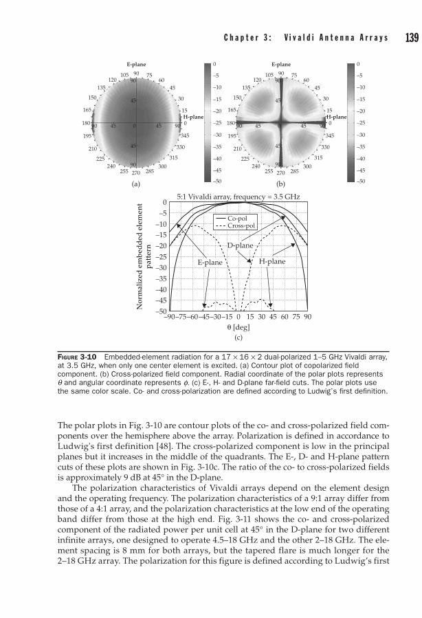
138 F r o n t i e r s i n a n t e n n a s : N e x t G e n e r a t i o n D e s i g n & e n g i n e e r i n g C h a p t e r 3 : V i v a l d i a n t e n n a a r r a y s 139
The polar plots in Fig. 3-10 are contour plots of the co- and cross-polarized field com-ponents over the hemisphere above the array. Polarization is defined in accordance to Ludwig's first definition [48]. The cross-polarized component is low in the principal planes but it increases in the middle of the quadrants. The E-, D- and H-plane pattern cuts of these plots are shown in Fig. 3-10c. The ratio of the co- to cross-polarized fields is approximately 9 dB at 45° in the D-plane.
The polarization characteristics of Vivaldi arrays depend on the element design and the operating frequency. The polarization characteristics of a 9:1 array differ from those of a 4:1 array, and the polarization characteristics at the low end of the operating band differ from those at the high end. Fig. 3-11 shows the co- and cross-polarized component of the radiated power per unit cell at 45° in the D-plane for two different infinite arrays, one designed to operate 4.5–18 GHz and the other 2–18 GHz. The ele-ment spacing is 8 mm for both arrays, but the tapered flare is much longer for the 2–18 GHz array. The polarization for this figure is defined according to Ludwig’s first
Figure 3-10 Embedded-element radiation for a 17 × 16 × 2 dual-polarized 1–5 GHz Vivaldi array, at 3.5 GHz, when only one center element is excited. (a) Contour plot of copolarized field component. (b) Cross-polarized field component. Radial coordinate of the polar plots represents q and angular coordinate represents f. (c) E-, H- and D-plane far-field cuts. The polar plots use the same color scale. Co- and cross-polarization are defined according to Ludwig’s first definition.
105120
135
150
165
180
195
210
225240
255 270 285300
315
330
345
15
30
4560
7590
0
E-plane
H-plane
90 45 0
45
90
45
90
45 90
0
–5
–10
–15
–20
–25
–30
–35
–40
–45
–50
105120
135
150
165
180
195
210
225240
255 270 285300
315
330
345
15
30
4560
7590
0
E-plane
H-plane
90 45 0
45
90
45
90
45 90
0
–5
–10
–15
–20
–25
–30
–35
–40
–45
–50(a) (b)
5:1 Vivaldi array, frequency = 3.5 GHz
E-plane
D-plane
H-plane
Co-polCross-pol
0–5
–10–15–20
–25–30
–35–40–45
–50–90–75–60–45–30–15 0
θ [deg](c)
15 30 45 60 75 90
Nor
mal
ized
em
bed
ded
ele
men
tp
atte
rn

140 F r o n t i e r s i n a n t e n n a s : N e x t G e n e r a t i o n D e s i g n & e n g i n e e r i n g C h a p t e r 3 : V i v a l d i a n t e n n a a r r a y s 141
definition [48]. This figure suggests that the cross-polarization increases with frequency and that long flares produce higher levels of cross-polarization than short flares. Both arrays in this figure are efficient radiators in the sense that the total radiated power is nearly equal to the input power. The copolarized power of the 9:1 array decreases sub-stantially at the higher frequencies because the input power is being radiated in the cross-polarized wave.
3.2 Design of Vivaldi Arrays
3.2.1 BackgroundDesign of ultra-wideband and wide-scan Vivaldi arrays is a challenging and time-consuming task because it requires optimization via full-wave computational elec-tromagnetics (CEM) methods. Practical Vivaldi arrays often have dimensions that span tens of wavelengths, while employing elements that involve features smaller than one one-hundredth of a wavelength. Therefore, Vivaldi arrays are multiscale electromagnetic structures that are notoriously difficult to analyze with full-wave methods [49]. Design based on the brute-force modeling of an entire array could quickly exhaust computer resources, and it will be impractically slow. In this section, a hierarchical design approach is suggested, which allows relatively fast design optimization and results in arrays that perform well at realistic array sizes and surrounding environments.
Figure 3-11 Normalized co- and cross-polarized radiated power per unit cell versus frequency for a 4:1 bandwidth (4.5–18 GHz) and a 9:1 bandwidth (2–18) infinite dual-polarized array, when both arrays are scanned 45° in the D-plane. Array elements are arranged in egg crate configuration. One polarization is driven and the other is terminated to 50 ohms.
Copolarization
φ = 45°
10:1 Bandwidth4:1 Bandwidth
Cross-polarization
0
–10
–20
–301 2 3 4 5 6 7 8 9 10 11 12 13 14 15 16 17 18 19
Frequency [GHz]
P rad
/U
nit c
ell [
dB
]

140 F r o n t i e r s i n a n t e n n a s : N e x t G e n e r a t i o n D e s i g n & e n g i n e e r i n g C h a p t e r 3 : V i v a l d i a n t e n n a a r r a y s 141
3.2.1.1 Design ApproachThe design approach in Fig. 3-12 is based on the efficiency of available computational tools for array analysis.
Infinite array analysis based on the unit cell method is the most efficient •way to incorporate mutual coupling effects into array analysis. Interior elements of a large phased array behave nearly the same as elements in an infinite array, but this analysis ignores truncation effects.
Infinite• × finite array analysis requires modeling one row (or column) of the array and captures the truncation effects that occur in the central regions of the array boundaries, which are assumed to be straight lines. The analysis is slower that the infinite array, but significantly faster that the full array simulation.
Finite• × finite array analysis models every element of the array simultaneously. This analysis captures all truncation effects, including important behavior near the corners of the array, but it is time-consuming and requires substantial computer resources, especially for finite Vivaldi arrays comprised of several hundred elements.
The design approach in Fig. 3-12 recognizes the importance of mutual coupling to array performance and the need to analyze several different element configurations during the early stages of array optimization. The antenna engineer starts from a set of electrical and mechanical specifications and chooses an initial element configuration to design in an infinite array environment. Because the infinite-array analysis is reason-ably efficient, many element variations can be tried to meet the desired performance and mechanical requirements. Performance at several scan angles also can be evaluated relatively quickly for the infinite array. The infinite-array design is first optimized for good impedance match at broadside excitation, and then scanning excitations in the E- and H-planes are considered. Impedance in the D-plane can be explicitly evaluated, but experience shows that it is approximately the average of E- and H-plane impedances.
Figure 3-12 Overview of the Vivaldi array design procedure.
Infinite array design
Prototype, test & deployFinite array design
Infinite × finite arraydesign
-Electrical specs(e.g., BW, scan volume, gain, etc.)-Mechanical specs(e.g., mounting platform, size, etc.)

142 F r o n t i e r s i n a n t e n n a s : N e x t G e n e r a t i o n D e s i g n & e n g i n e e r i n g C h a p t e r 3 : V i v a l d i a n t e n n a a r r a y s 143
When an element is found that has acceptable performance in the infinite array, it must be evaluated in a finite array to determine if changes due to truncation effects are acceptable. Analyzing one row or one column as a infinite × finite array provides initial information about the element's susceptibility to truncation effects. If the perfor-mance is not satisfactory, redesign of the element may reduce its sensitivity to the effects of truncation.
Finally, the proposed element is analyzed in a finite × finite array to determine if the corners cause unacceptable degradation of element performance. If the finite × finite array simulation results are satisfactory, a prototype array can be manufactured with reasonable confidence that it will work well.
3.2.1.2 Array Analysis Techniques
3.2.1.2.1 Infinite × Infinite Array Analysis The infinite array environment approximates well a large array, but more importantly leads to significant computational savings that expedite the design. An infinite array under uniform amplitude and progressive phase excitation produces periodic fields having the same periodicity and phase pro-gression as the excitation. Therefore, one periodic unit cell is sufficient to describe the entire array. This is a loosely stated version of the Floquet theorem [50] that through ap-propriate periodic boundary conditions (PBC) enable infinite array unit cell simulations. The infinite array approximation incorporates mutual coupling, but it ignores trunca-tion effects. Many analysis methods have been proposed to analyze infinite array unit cells using frequency [12], [13], [51] and time-domain CEM methods [52], [53]. The re-sults in Section 3.2.2 were obtained using the periodic boundary finite difference time domain (PB-FDTD) method [52]. In Sections 3.2.3 and 3.2.4, the frequency domain FEM with the “cement” enforcement of PBCs [51] is used.
3.2.1.2.2 Infinite × Finite Array Analysis Because truncation effects and interactions with nearby structures involve the time-consuming and memory demanding simula-tion of the full, finite array, infinite × finite array (“stick”) approximation is used. An array comprised of infinitely many rows (or columns) of the actual array is analyzed. The analysis correctly models the array edges at the ends of the sticks, but ignores the effects of corners and of interactions between edges other than the two opposing edges of the infinite × finite array.
The results in Sections 3.2.3 and 3.2.4 were obtained by using a special, full-wave domain decomposition FEM (DD-FEM) method that reduces computational overhead by exploiting geometrical repetitions in the finite-array dimension, without introducing extra approximations (mutual coupling and edge truncation effects are rigorously included). The method involves the combination of the DD-FEM method [54] with the “cement” method for enforcing periodic boundary conditions [55]. This analysis is used to evaluate the effects of array truncations and interactions with the environment (such as nearby cavity walls) on the impedance and radiation pattern.
3.2.1.2.3 Finite × Finite Array Analysis Traditional method-of-moments (MoM), FEM, and FDTD methods can analyze finite × finite Vivaldi arrays comprised of a few tens of elements. Over the years several specially tailored full-wave approaches have been developed to analyze finite arrays [56]–[62]. In Sections 3.2.3 and 3.2.4 a nonconforming DD-FEM method based on the work in [58], [54] is used to accurately assess the perfor-mance of practical wideband arrays. DD-FEM is among the best full-wave CEM tools

142 F r o n t i e r s i n a n t e n n a s : N e x t G e n e r a t i o n D e s i g n & e n g i n e e r i n g C h a p t e r 3 : V i v a l d i a n t e n n a a r r a y s 143
available at this time because it is as general and versatile as traditional FEM, it is accurate, it has been extensively validated, and it is numerically efficient both in terms of memory and time. Moreover, DD-FEM is known for very good parallel scalability that further speeds up computations. All the results in Sections 3.2.3 and 3.2.4 exploit fully parallel versions of DD-FEM.
3.2.2 Infinite Array Element Design for Wide Bandwidth
3.2.2.1 Element Spacing and DepthThe element spacing of a scanning phased array is usually set to be one-half wavelength at the upper operating frequency. This ensures that the peak of the grating lobe is excluded from visible space as the array scans out to 90° in all planes. Even for element spacing of l/2, the grating lobe of small arrays with wide beam widths can substantially increase the far-out sidelobe level.
Vivaldi antenna arrays have an additional restriction on element spacing, even if the array does not scan. The region between the Vivaldi elements forms a waveguide that supports propagating modes when the element spacing is approximately l/2 or greater. When these modes begin to propagate, the array impedance changes radically due to resonances associated with these modes.
Fig. 3-13 shows the waveguide responsible for the resonance and a typical VSWR plot including frequencies above the intended operating frequency. The metallization at the bottom of the array in Fig. 3-13a forms an air-filled, square waveguide. A con-ducting ground plane at the bottom of the array terminates this waveguide in a short circuit. The waveguide’s width is slightly less than the element spacing (because of
Figure 3-13 Internal waveguide in region between Vivaldi antennas. (a) Vivaldi antenna metallization forms an air-filled waveguide with tapered slot loading in its walls. (b) VSWR for broadside beam of array designed for 1.0–5.5 GHz showing waveguide resonances above the intended operating frequency. D = 9.7 cm, a = b = 2.7 cm, substrate e
r = 2.2, thickness = 0.315 cm.
(a)
4
3.5
3
2.5
2
1.5
0.5 1.5 2.5 3.5 4.5 5.5 6.5 7.5 8.51
Frequency [GHz](b)
VSW
R
Intended operation range
Egg crate “waveguide”

144 F r o n t i e r s i n a n t e n n a s : N e x t G e n e r a t i o n D e s i g n & e n g i n e e r i n g C h a p t e r 3 : V i v a l d i a n t e n n a a r r a y s 145
the element thickness), so the lowest mode begins to propagate at a frequency slightly higher than where the element spacing is l/2. In the upper region of the array, the waveguide walls are “loaded” by tapered slots, but a mode that resembles the TE10 waveguide mode can still exist in this region of the periodic array. At certain fre-quencies, this mode “resonates” to create impedance anomalies that destroy array performance. If the array is not backed by a ground plane, in addition to the reso-nances, operation close to the waveguide cutoff has adverse effects on the radiation pattern. To demonstrate that, the near fields of a 16 × infinite dual-polarized array without a ground are plotted in Fig. 3-14 from 1 GHz to 6 GHz with 1 GHz increments. At frequencies below 5 GHz (far from cutoff), only forward radiation is observed; however, above 5 GHz significant back radiation is observed from the excitation of the internal waveguides. These waveguide resonance and back radiation phenomena re-strict the spacing of Vivaldi elements to be less than approximately one-half wavelength at the highest operating frequency (<lhi/2), even if the array does not scan far from broadside.
Experience shows that the lowest frequency of operation occurs when the depth of the Vivaldi elements (ground plane to aperture) is approximately one-quarter wave-length. That is, D ~ llo/4. Combining this result with the minimum spacing, a ~ l hi/2, provides a key design relationship for Vivaldi arrays,
fhi/flo ~ 2 × (D/a) (3-1)
This formula has been verified for array bandwidths from 2:1 up to 10:1 and for stripline-fed antennas fabricated on dielectric substrates with relative permittivities in the range 2 to 3, which is typical of many microwave substrates. Using this relation-ship, a Vivaldi array operating over 10:1 bandwidth should have an element spacing of approximately 0.5 wavelengths at the highest frequency (to prevent anomalies and grating lobes) and a depth of approximately 2.5 wavelengths at the highest frequency, i.e., D/a = 5.
The depth of the Vivaldi elements can be reduced by using a substrate with higher permittivity. The 10:1 bandwidth can be covered with a Vivaldi element that is only
Figure 3-14 Back radiation from the internal waveguide region. Near-fields of a 16 × infinite dual-polarized Vivaldi array between 1–6 GHz with 1 GHz increments start from the top left and end at the bottom right. Only the horizontal elements are excited, and the last two rows of elements are “dummy.”
M(V/m^2)500.
232.
108.
50.0
23.2
10.8
5.00

144 F r o n t i e r s i n a n t e n n a s : N e x t G e n e r a t i o n D e s i g n & e n g i n e e r i n g C h a p t e r 3 : V i v a l d i a n t e n n a a r r a y s 145
1.5 wavelengths deep (D/a = 3) if the relative permittivity is increased to 10–12. However, care must be taken when using high permittivity substrates because impedance anoma-lies may enter into the band of operation.
To illustrate this relationship of bandwidth to D/a, Fig. 3-15 shows the VSWR of three arrays of differing depths, but all with spacing a = 8 mm. The spacing of 8 mm corresponds to l/2 at 18.75 GHz. Using equation (3-1) and the values of antenna depth indicated in Fig. 3-15 yields expected values of flo for these three cases: 1.67, 3.33, and 6.67 GHz. The actual values are 1.64, 3.47, and 6.60 GHz.
Therefore, a good starting point from which to optimize the element design for a particular application is
D/a ~ 0.5 fhi/flo . (3-2)
3.2.2.2 Opening Rate of Exponential FlareOnce the aspect ratio of the Vivaldi element, D/a, is fixed, the type and opening rate of the flared slotline is an important parameter to control Vivaldi array performance. In this work, the Vivaldi exponential flare is defined by
y = C1e R Z + C2
where the constants C1 and C2 are chosen so the exponential flare passes through the end points (y1, z1) and (y2, z2). See Fig. 3-16.
C
y y
e eRz Rz11
2 1=
--
2
Cy e y e
e e
Rz Rz
Rz Rz22
1
2 1=
--
12
Figure 3-15 VSWR of three Vivaldi arrays (infinite) with element spacing of 8 mm, broadside beam. Elements are stripline-fed and dielectric e
r = 2.2. The parameter is array depth, ground
plane to aperture, and each array is optimized for bandwidth (VSWR<2) at broadside.
3
2.5
2
1.5
1
VSW
R
2 6 8 10 12 14 16 18 204Frequency (GHz)
DD = 11.25 mmD = 22.5 mmD = 45 mm
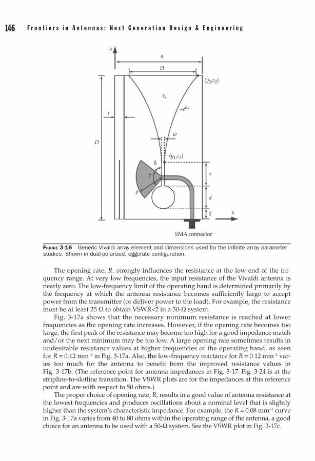
146 F r o n t i e r s i n a n t e n n a s : N e x t G e n e r a t i o n D e s i g n & e n g i n e e r i n g C h a p t e r 3 : V i v a l d i a n t e n n a a r r a y s 147
The opening rate, R, strongly influences the resistance at the low end of the fre-quency range. At very low frequencies, the input resistance of the Vivaldi antenna is nearly zero. The low-frequency limit of the operating band is determined primarily by the frequency at which the antenna resistance becomes sufficiently large to accept power from the transmitter (or deliver power to the load). For example, the resistance must be at least 25 Ω to obtain VSWR<2 in a 50-Ω system.
Fig. 3-17a shows that the necessary minimum resistance is reached at lower frequencies as the opening rate increases. However, if the opening rate becomes too large, the first peak of the resistance may become too high for a good impedance match and/or the next minimum may be too low. A large opening rate sometimes results in undesirable resistance values at higher frequencies of the operating band, as seen for R = 0.12 mm-1 in Fig. 3-17a. Also, the low-frequency reactance for R = 0.12 mm-1 var-ies too much for the antenna to benefit from the improved resistance values in Fig. 3-17b. (The reference point for antenna impedances in Fig. 3-17–Fig. 3-24 is at the stripline-to-slotline transition. The VSWR plots are for the impedances at this reference point and are with respect to 50 ohms.)
The proper choice of opening rate, R, results in a good value of antenna resistance at the lowest frequencies and produces oscillations about a nominal level that is slightly higher than the system’s characteristic impedance. For example, the R = 0.08 mm-1 curve in Fig. 3-17a varies from 40 to 80 ohms within the operating range of the antenna, a good choice for an antenna to be used with a 50-Ω system. See the VSWR plot in Fig. 3-17c.
Figure 3-16 Generic Vivaldi array element and dimensions used for the infinite array parameter studies. Shown in dual-polarized, eggcrate configuration.
z
(y2,z2)
(y1,z1)
a
H
εr
t
D
s
w
d
g x
SMA connector
~eRz
γ
δ
ρ
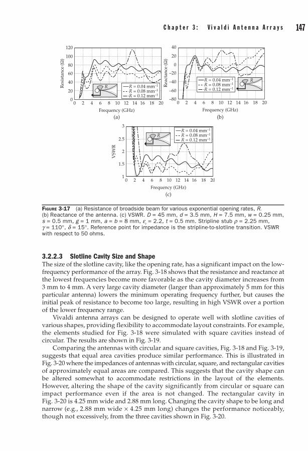
146 F r o n t i e r s i n a n t e n n a s : N e x t G e n e r a t i o n D e s i g n & e n g i n e e r i n g C h a p t e r 3 : V i v a l d i a n t e n n a a r r a y s 147
3.2.2.3 Slotline Cavity Size and ShapeThe size of the slotline cavity, like the opening rate, has a significant impact on the low-frequency performance of the array. Fig. 3-18 shows that the resistance and reactance at the lowest frequencies become more favorable as the cavity diameter increases from 3 mm to 4 mm. A very large cavity diameter (larger than approximately 5 mm for this particular antenna) lowers the minimum operating frequency further, but causes the initial peak of resistance to become too large, resulting in high VSWR over a portion of the lower frequency range.
Vivaldi antenna arrays can be designed to operate well with slotline cavities of various shapes, providing flexibility to accommodate layout constraints. For example, the elements studied for Fig. 3-18 were simulated with square cavities instead of circular. The results are shown in Fig. 3-19.
Comparing the antennas with circular and square cavities, Fig. 3-18 and Fig. 3-19, suggests that equal area cavities produce similar performance. This is illustrated in Fig. 3-20 where the impedances of antennas with circular, square, and rectangular cavities of approximately equal areas are compared. This suggests that the cavity shape can be altered somewhat to accommodate restrictions in the layout of the elements. However, altering the shape of the cavity significantly from circular or square can impact performance even if the area is not changed. The rectangular cavity in Fig. 3-20 is 4.25 mm wide and 2.88 mm long. Changing the cavity shape to be long and narrow (e.g., 2.88 mm wide × 4.25 mm long) changes the performance noticeably, though not excessively, from the three cavities shown in Fig. 3-20.
Figure 3-17 (a) Resistance of broadside beam for various exponential opening rates, R. (b) Reactance of the antenna. (c) VSWR. D = 45 mm, d = 3.5 mm, H = 7.5 mm, w = 0.25 mm, s = 0.5 mm, g = 1 mm, a = b = 8 mm, e
r = 2.2, t = 0.5 mm. Stripline stub r = 2.25 mm,
g = 110°, d = 15°. Reference point for impedance is the stripline-to-slotline transition. VSWR with respect to 50 ohms.
120
100
80
60
40
20
0
Res
ista
nce
(Ω)
20 6 8 10 12 14 16 18 204
Frequency (GHz)(a) (b)
R = 0.04 mm–1
R = 0.08 mm–1
R = 0.12 mm–1
40
20
0
–20
–40
–60
–80
Rea
ctan
ce (Ω
)
20 6 8 10 12 14 16 18 204
Frequency (GHz)
R = 0.04 mm–1
R = 0.08 mm–1
R = 0.12 mm–1
RR
3
2.5
2
1.5
1
VSW
R
20 6 8 10 12 14 16 18 204
Frequency (GHz)
(c)
R = 0.04 mm–1
R = 0.08 mm–1
R = 0.12 mm–1R

148 F r o n t i e r s i n a n t e n n a s : N e x t G e n e r a t i o n D e s i g n & e n g i n e e r i n g C h a p t e r 3 : V i v a l d i a n t e n n a a r r a y s 149
3.2.2.4 Stripline Stub Length and AngleThe open-circuited stub on the balun changes the reactance of the antenna with very little impact on the resistance. Altering the shape of the stub has some effect on its reactance versus frequency, but radial stubs have been found to work well in many wide band-width array designs. By adjusting the radius, r, and angle, g, of the radial stub, the an-tenna’s impedance can be brought close to the real axis over a wide range of frequencies.
Fig. 3-21 shows the resistance and reactance of one of the antennas in Fig. 3-18 as the stripline stub’s radius is varied. The resistances, Fig. 3-21a, differ by only a few ohms over the entire frequency range for these three stub lengths. However, the reac-tances, Fig. 3-21b, change by 10–20 ohms over much of the frequency range, and by more than 50 ohms at the lowest frequencies.
Fig. 3-22 shows the resistance and reactance of the same antenna as the stub angle is changed. The primary parameter that is varied is the stub angle, g, but the stub tilt, d, is changed also to keep the stub positioned nicely between the slotline cavity and the Vivaldi flare. Resistances for various stub angles are shown in Fig. 3-22a and are very nearly the same over the frequency range, but the reactances, shown in Fig. 3-22b, vary greatly over the frequency range. The reactance changes only a small amount at the upper frequencies, but it changes a lot at the lower frequencies.
Figure 3-18 Resistance and reactance for various circular cavity diameters, d. Infinite array, broadside beam. R = 0.06 mm-1, D = 45.0 mm, H = 7.5 mm, w = 0.25 mm, s = 0.5 mm, a = b = 8 mm, e
r = 2.2, t = 0.5 mm. Stripline stub r = 2.25 mm, g = 110°, d = 15°.
d = 3 mmd = 4 mmd = 5 mm
d = 3 mmd = 4 mmd = 5 mm
d
120
100
80
60
40
20
020 6 8 10 12 14 16 18 204
Frequency (GHz)
(a) (b)
d
Res
ista
nce
(Ω)
40200
–40–20
–60–80
–120–100
20 6 8 10 12 14 16 18 204Frequency (GHz)
Rea
ctan
ce (Ω
)
Figure 3-19 Resistance and reactance for various square cavities with side length L. Infinite array, Broadside beam. R = 0.06 mm-1, D = 45.0 mm, H = 7.5 mm, w = 0.25 mm, s = 0.5 mm, a = b = 8 mm, e
r = 2.2, t = 0.5 mm. Stripline r = 2.25 mm, g = 110°, d = 15°.
100
80
60
40
20
020 6 8 10 12 14 16 18 204
Frequency (GHz)
(a) (b)
Res
ista
nce
(Ω)
40200
–40–20
–60–80
–120–100
2 6 8 10 12 14 16 18 204Frequency (GHz)
Rea
ctan
ce (Ω
)
L L
L = 2.5 mmL = 3.0 mmL = 4.0 mm
L = 2.5 mmL = 3.0 mmL = 4.0 mm

148 F r o n t i e r s i n a n t e n n a s : N e x t G e n e r a t i o n D e s i g n & e n g i n e e r i n g C h a p t e r 3 : V i v a l d i a n t e n n a a r r a y s 149
Adjusting the radius, r, and the angle, g, of the stub allows the antenna reactance to be tuned near zero over a wide frequency range.
3.2.2.5 Substrate Thickness and PermittivitySince antenna efficiency is usually an important performance parameter, a high-quality microwave substrate is typically used to fabricate the array elements. All of the design examples in this section are stripline-fed antennas with the Vivaldi elements formed as bilateral slotlines. The choice of substrate thickness depends on the desired perfor-mance and the allowed weight. Thin substrates are lower weight, but they are not as
Figure 3-20 Comparison of antenna impedances with circular, square, and rectangular cavities with areas of approximately 12.4 mm2
Res
ista
nce
(Ω)
100
80
60
40
20
02 6 8 10 12 14 16 18 204
Frequency (GHz)
(a) (b)
20
0
–40
–20
–60
–80
–120
–100
2 6 8 10 12 14 16 18 204
Frequency (GHz)
Rea
ctan
ce (Ω
)
Circle, diameter = 4.0Square, 3.5 × 3.5Rectangle, 4.25W × 2.88L
Circle, diameter = 4.0Square, 3.5 × 3.5Rectangle, 4.25W × 2.88L
VSW
R
3
2.5
2
1.5
12 6 8 10 12 14 16 18 204
Frequency (GHz)
(c)
Circle, diameter = 4.0Square, 3.5 × 3.5Rectangle, 4.25W × 2.88L
Circle, diameter = 4.0Square, 3.5 × 3.5Rectangle, 4.25W × 2.88L
Figure 3-21 Resistance and reactance for various radial stub lengths, r. Infinite array, broadside beam. R = 0.06 mm-1, D = 45.0 mm, d = 4.0 mm, H = 7.5 mm, w = 0.25 mm, s = 0.5 mm, a = b = 8 mm, e
r = 2.2, t = 0.5 mm. Stripline stub g = 110°, d = 15°.
100 40200
–20–40–60–80
–100
80
60
40
20
00 2 4 6 8 10 12 14 16 18 20
Frequency (GHz)0 2 4 6 8 10 12 14 16 18 20
Frequency (GHz)
Res
ista
nce
(Ω)
Rea
ctan
ce (Ω
)
ρ ρ
ρ = 1.75 mmρ = 2.25 mm
(a) (b)
ρ = 2.75 mm
ρ = 1.75 mmρ = 2.25 mmρ = 2.75 mm
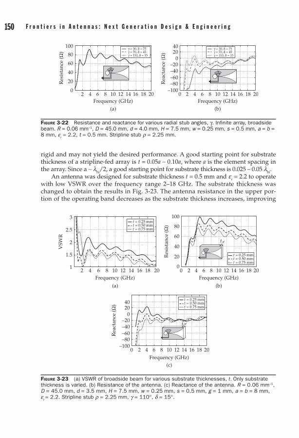
150 F r o n t i e r s i n a n t e n n a s : N e x t G e n e r a t i o n D e s i g n & e n g i n e e r i n g C h a p t e r 3 : V i v a l d i a n t e n n a a r r a y s 151
rigid and may not yield the desired performance. A good starting point for substrate thickness of a stripline-fed array is t = 0.05a – 0.10a, where a is the element spacing in the array. Since a ~ lhi/2, a good starting point for substrate thickness is 0.025 – 0.05 lhi.
An antenna was designed for substrate thickness t = 0.5 mm and er = 2.2 to operate with low VSWR over the frequency range 2–18 GHz. The substrate thickness was changed to obtain the results in Fig. 3-23. The antenna resistance in the upper por-tion of the operating band decreases as the substrate thickness increases, improving
Figure 3-22 Resistance and reactance for various radial stub angles, g. Infinite array, broadside beam. R = 0.06 mm-1, D = 45.0 mm, d = 4.0 mm, H = 7.5 mm, w = 0.25 mm, s = 0.5 mm, a = b = 8 mm, e
r = 2.2, t = 0.5 mm. Stripline stub r = 2.25 mm.
100 40200
–20–40–60–80
–100
80
60
40
20
04 6 8 10 12 14 16 18 20
Frequency (GHz)0 2 4 6 8 10 12 14 16 18 20
Frequency (GHz)
Rea
ctan
ce (Ω
)
Res
ista
nce
(Ω)
γ = 30, δ = 75γ = 70, δ = 45γ = 110, δ = 15
γ = 30, δ = 75γ = 70, δ = 45γ = 110, δ = 15
(a) (b)
γγ
2
Figure 3-23 (a) VSWR of broadside beam for various substrate thicknesses, t. Only substrate thickness is varied. (b) Resistance of the antenna. (c) Reactance of the antenna. R = 0.06 mm-1, D = 45.0 mm, d = 3.5 mm, H = 7.5 mm, w = 0.25 mm, s = 0.5 mm, g = 1 mm, a = b = 8 mm, e
r = 2.2. Stripline stub r = 2.25 mm, g = 110°, d = 15°.
(a)
3
2.5
2
1.5
1
Frequency (GHz)
VSW
R
40200
–20–40–60–80
–100
Frequency (GHz)
Rea
ctan
ce (Ω
)
(c)
(b)
t = 0.50 mmt = 0.75 mm
t = 0.25 mm
t = 0.50 mmt = 0.75 mm
t = 0.25 mm
t = 0.50 mmt = 0.75 mm
t = 0.25 mm
t
Frequency (GHz)
Res
ista
nce
(Ω)
t
100
80
60
40
20
00 2 4 6 8 10 12 14 16 18 20
0 2 4 6 8 10 12 14 16 18 20
2 4 6 8 10 12 14 16 18 20

150 F r o n t i e r s i n a n t e n n a s : N e x t G e n e r a t i o n D e s i g n & e n g i n e e r i n g C h a p t e r 3 : V i v a l d i a n t e n n a a r r a y s 151
this antenna’s match to 50 ohms at higher frequencies. The initial rise of the resistance near the low end of the operating band is not affected much by thickness, so the low-est frequency for which the antenna can be matched (by adjusting its low-frequency reactance) is not affected by thicknesses in the range shown. The VSWR of the antenna with t = 0.75 mm is relatively high below 3 GHz due primarily to large capacitive reactance at low frequencies. Some of this effect can be offset by changing the strip-line stub as noted above.
Increasing the permittivity of the dielectric substrate creates effects resembling those of a longer antenna (larger D). Some of these effects might be anticipated since the dielectric loading shortens the “guided” wavelength along the flared slot and in-creases the capacitance per unit length of the slotline. Fig. 3-24(a) shows the resis-tance of an antenna for relative permittivties of 2.2, 9.8, and 16. Several trends are evident:
1. Increasing the permittivity lowers the frequency at which the resistance attains a usable value.
2. Increasing the permittivity reduces the frequency separation of peaks in the resistance.
3. Increasing the permittivity reduces the average value of the resistance throughout most of the operating band.
4. Increasing the permittivity can result in anomalies within the operating band.
The lower average resistance that accompanies higher er can be beneficial for matching the Vivaldi array to 50 Ohms, since arrays fabricated with low permittivity substrates tend to work best for generator impedances around 75 ohms. In the exam-ples of Fig. 3-24, the antenna resistance for highest er is too low for a good match to 50 ohms, but this can be corrected by increasing the slotline width, w, near the transition. Larger w yields a higher slotline characteristic impedance which influences the antenna resistance.
For er = 16, there is a strongly excited resonance near 17.5 GHz that limits perfor-mance at the upper end of the desired operating band. For er = 9.8, this resonance is weakly excited. For the higher values of er, there are other resonances at lower frequencies, but these are only weakly excited and probably will not degrade the performance of the array.
Figure 3-24 Effects of substrate permittivity, er. (a) Resistance (b) Reactance. R = 0.125 mm-1,
D = 24.0 mm, d = 2.5 mm, H = 7.5 mm, w = 0.25 mm, s = 0.5 mm, g = 1 mm, a = b = 8 mm, t = 0.5 mm. Stripline stub r = 2.0 mm, g = 110°, d = 15°.
εr = 2.2εr = 9.8εr = 16
εr = 2.2εr = 9.8εr = 16
120
100
80
60
40
20
00
60
40
20
–20
–40
–60
0
2 4 6 8 10 12 14 16 18 20Frequency (GHz)
2 4 6 8 10 12 14 16 18 20Frequency (GHz)
Res
ista
nce
(Ω)
Rea
ctan
ce (Ω
)
(a) (b)

152 F r o n t i e r s i n a n t e n n a s : N e x t G e n e r a t i o n D e s i g n & e n g i n e e r i n g C h a p t e r 3 : V i v a l d i a n t e n n a a r r a y s 153
The antenna reactances, Fig. 3-24b, reveal the anomalies observed in the resistance plots and the reduced frequency spacing of the oscillations. The average value of the reactance over the operating band is not affected greatly by the substrate permittivity, and some compensation of the average slope of the reactance can be achieved by altering the design of the stripline stub.
3.2.3 Infinite × Finite Array Truncation EffectsThe infinite array design and the resulting phenomenology in previous sections include mutual coupling but ignore truncation effects introduced by the discontinuities at the ends of a finite array. These effects alter the impedance and far-field radiation char-acteristics of the array when compared to the infinite counterpart. Currently, no sim-ple theory exists that quantitatively predicts truncation phenomena in complicated arrays such as Vivaldi arrays, so full-wave computations are the only way to reliably predict finite array performance. In this section, full-wave methods will be used to study truncation effects for infinite × finite array configurations.
This section will use a dual-polarized element design as a test case to study truncations. The element is based on the general topology presented in Fig. 3-16, with R = 0.03 mm-1, D = 97.0 mm, d = 8.47 mm, H = 18.6 mm, w = 1.1 mm, s = 0 mm, g = 15.94 mm, a = b = 30.17 mm, t = 3.15 mm, er = 2.2, r = 9.0 mm, g = 88°, d = 20°. All array elements are con-nected to 50-ohm ports at the base of the element, and the VSWR or active reflection coefficient results are referenced to 50 ohms. The arrays are always excited with uni-form amplitude and progressive phase, and real dielectric materials but infinitely thin perfect electric conductors (PECs) have been used in the models. The computa-tional domain is truncated with absorbing boundary conditions placed approximately one wavelength away from the array at the lowest frequency, and the FEM meshes have been obtained through 8 steps of adaptive mesh refinement based on algorithms pre-sented in [63], leading to 650,000 second order FEM unknowns in each element (includes both polarizations). Results from similar computational setups and methods have been repeatedly validated with measurements and other methods [54].
Apart from element design, truncation effects on infinite × finite arrays depend on array size, edge element treatment, and the presence of structures in close proximity to the array. These effects will be quantified in terms of the active (under uniform broadside excitation) VSWR.
3.2.3.1 Array SizeThe size of a finite Vivaldi array strongly influences the element impedances. Truncation effects on Vivaldi arrays significantly affect elements within one to two wavelengths of the edges of the array. Therefore, in electrically small arrays with sizes less than four wavelengths, the majority of elements are affected by truncations, whereas in electrically large arrays with many elements in each dimension, most of the elements are minimally affected by truncations. Because Vivaldi arrays are designed with half-wavelength periodicity at the highest frequency, they operate at electrically very small periodicities at the low end of the band. Therefore, a larger number of elements is affected by trunca-tions at the lower end of the operating band rather than at the upper end.
To quantify these effects, three infinite × finite dual-polarized arrays are considered. In the finite dimension each array has 8, 16, and 32 elements, respectively. The arrays are dual-polarized, but only one polarization is excited while the other is terminated in 50 ohms. The active elements are chosen to be polarized in the direction of the finite array (E-plane finite array). Results from the H-plane case are generally similar to the

152 F r o n t i e r s i n a n t e n n a s : N e x t G e n e r a t i o n D e s i g n & e n g i n e e r i n g C h a p t e r 3 : V i v a l d i a n t e n n a a r r a y s 153
E-plane case, and will be shown only once to demonstrate the difference in the behav-ior of the edge elements in Section 3.2.3.2.
The VSWR versus frequency of the 8, 16, and 32 arrays are plotted in Fig. 3-25. In a finite × infinite array, each individual element of the “stick” has different VSWR plot-ted with small circles in Fig. 3-25, and at a given frequency the VSWRs of the elements spread over a range of values. To quantify the spread between individual element VSWRs at each frequency, each plot depicts the average VSWR among stick elements with a solid line, and the average ± one standard deviation VSWR curves with dashed lines. The infinite array prediction is plotted with dots. Overall, the average lines track well the infinite array VSWR. The biggest difference between the infinite array and the average VSWR occurs at lower frequencies and for the smallest size array. The one standard deviation curve from the average tends to be more concen-trated around the average as the array size and frequency increases, with one excep-tion around 5.5 GHz, where the egg crate waveguide mode is close to cut-off. Al-though the one standard deviation overall decreases with increasing array size, the maximum deviation from the infinite array remains approximately the same regardless of size.
Dual-pol. Vivaldi 16E × ∞ arrayin free-space
Dual-pol. Vivaldi 8E × ∞ arrayin free-space
43.83.63.43.2
32.82.62.42.2
21.81.61.41.2
1
43.83.63.43.2
32.82.62.42.2
21.81.61.41.2
11 1.5 2 2.5 3 3.5 4 4.5 5 5.5 1 1.5 2 2.5 3 3.5 4 4.5 5 5.5
VSW
R
VSW
R
Freq [GHz] Freq [GHz]
Infinite arrayE[VSWR]E[VSWR]+(Var[VSWR])1/2
E[VSWR]–(Var[VSWR])1/2
Element VSWR
Infinite arrayE[VSWR]E[VSWR]+(Var[VSWR])1/2
E[VSWR]–(Var[VSWR])1/2
Element VSWR
(a) (b)Dual-pol. Vivaldi 32E × ∞ array
in free-space4
3.83.63.43.2
32.82.62.42.2
21.81.61.41.2
11 1.5 2 2.5 3 3.5 4 4.5 5 5.5
VSW
R
Freq [GHz]
Infinite arrayE[VSWR]E[VSWR]+(Var[VSWR])1/2
E[VSWR]–(Var[VSWR])1/2
Element VSWR
(c)
Figure 3-25 VSWR statistical analysis of various size finite × infinite dual-polarized Vivaldi arrays. (a) 8 × infinite array, (b) 16 × infinite array, and (c) 32 × infinite array.

154 F r o n t i e r s i n a n t e n n a s : N e x t G e n e r a t i o n D e s i g n & e n g i n e e r i n g C h a p t e r 3 : V i v a l d i a n t e n n a a r r a y s 155
The plots in Fig. 3-25 provide a good overall metric for quantifying the effects of truncations on VSWR, but do not provide any information about which elements devi-ate the most from the infinite array. This information is shown in Fig. 3-26 that plots the element VSWR distribution in space and frequency for the three arrays. The horizontal axis represents the element number from left to right, and the vertical axis represents frequency. Each colored tile indicates the port VSWR of the respective element and frequency. It is clear from all three arrays that the frequencies between 1 and 2 GHz are the most affected by the truncations. At these frequencies most of the array elements have higher VSWR that fluctuates the most, and a periodic pattern (every 5 elements) along the horizontal axis is noticeable. Above 2.5 GHz all arrays operate similar to the infinite array, but even at these frequencies, the frequency behavior of edge elements differs from the interior elements. In summary, the edge elements in infinite × finite arrays always deviate from the infinite array prediction, especially at lower frequencies.
Figure 3-26 VSWR distribution across the array “Stick” (horizontal axis) vs. Frequency (vertical axis) for an 8 × infinite, 16 × infinite, and 32 × infinite dual-polarized Vivaldi array, excited with broadside uniform excitations. The finite array is in the E-plane.
65.5
54.5
43.5
32.5
21.5
1 1 2 3 4 5 6 7 8Element index
1 2 3 4 5 6 7 8 9 10 11 12 13 14 15 16
2468 10 12 14 16 18 20 22 24 26 28 30 321
1.5
2
2.5
3
Element index
Element index
VSWR, 5:1 Vivaldi array, arrayin free-space
VSWR, 5:1 Vivaldi array, arrayin free-space
VSWR, 5:1 Vivaldi array, arrayin free-space
Freq
uenc
y [G
Hz]
65.5
54.5
43.5
32.5
21.5
1
Freq
uenc
y [G
Hz]
65.5
54.5
43.5
32.5
21.5
1
Freq
uenc
y [G
Hz]
(a) (b)
(c)

154 F r o n t i e r s i n a n t e n n a s : N e x t G e n e r a t i o n D e s i g n & e n g i n e e r i n g C h a p t e r 3 : V i v a l d i a n t e n n a a r r a y s 155
The most severely affected elements tend to be found 1–4 rows (or approximately one to two wavelengths) around the edges of the array, which is consistent with the observations of Holter et al. [64] for single polarized Vivaldi arrays. This observation will become more pronounced in finite × finite arrays in Section 3.2.4.
3.2.3.2 Edge Treatment and Proximity EffectsTo better understand and perhaps control truncation effects, this section will present results from some common edge treatment techniques and interactions with structures in the proximity of the array. One edge treatment case and two proximity effect cases will be compared with the baseline case of a stand-alone finite × infinite array, shown in Fig. 3-27a. The edge treatment case is shown in Fig. 3-27b, where two rows of “dummy” elements are added on each side of the active array region. This approach is easy to implement and it is intended to create an environment for the edge elements resembling that of the middle elements. The first proximity effect case is shown in Fig. 3-27c and consists of the backing of the array by a finite PEC plate with edges close to the array edges. This case will quantify the effects of the plate's edge diffractions on the element impedance. Lastly, the case of a Vivaldi array recessed in a large cavity, shown in Fig. 3-27d, will be used to reveal potential interactions with the natural modes of the cavity. The cavity sidewalls are placed approximately one element away from the array and the aperture of the cavity is flush with the top of the array. Similarly to the PEC plate case, the cavity back plate is electrically connected to the element conductors.
Results from these geometries are plotted in Fig. 3-28 that show the VSWR distri-bution along the array at two frequencies and three array sizes. Overall, the dummy ele-ment and finite ground plate cases follow well the baseline case of the array in free space, indicating that the addition of “dummy” elements, or diffractions from the plate edges, have little or no impact on element impedance. However, the cavity case deviates from rest of the cases. From the analysis of various frequencies (not shown here), it is observed that the deviation decreases with increasing frequency. For this
Figure 3-27 Configurations used to demonstrate some edge treatment and proximity effects on infinite × finite Vivaldi arrays. (a) Array in free-space. (b) Array with two rows of “dummy” elements at each edge. (c) Array with finite ground plane. (d) Array recessed in a cavity.
(a)
ZL ZLZL ZL
(b)
(c)
(d)2 Rows of
dummy elms
Infinite Infinite
Cavity
Finiteground plane

156 F r o n t i e r s i n a n t e n n a s : N e x t G e n e r a t i o n D e s i g n & e n g i n e e r i n g C h a p t e r 3 : V i v a l d i a n t e n n a a r r a y s 157
polarization (only elements perpendicular to the cavity sidewalls are excited) the cavity case did not indicate any signs of cavity induced resonances in the band. In all finite × infinite array cases the element VSWR fluctuates around the infinite array pre-diction (shown with a solid line). Notably, at some frequencies (e.g., 2 GHz in Fig. 3-28) the edge elements are better matched than the infinite array predictions or the center elements, whereas at other frequencies the same elements have large VSWR. These phe-nomena may be attributed to complex interference (e.g., standing wave) phenomena between waves launched by the edge discontinuities. To compensate for these adverse truncation effects, the design at the infinite array stage must maintain very low VSWR (over-designed) throughout the band.
The cavity has slightly more effect when elements polarized parallel to the cav-ity walls are excited. The H-polarized excitation for both the free-space and cavity case VSWR versus frequency are plotted side-by-side in Fig. 3-29. In both cases the active VSWR plots are similar, but overall, the cavity case shows higher VSWR lev-els at the low end of the band. For this polarization (H-plane finite array), the edge elements show a distinct resonance behavior around 3.75 GHz for both free-space and cavity cases. It is believed that this is of the same nature as the gap-induced resonances described in Section 3.1.5, that now occur at the array (or subarray) level. This hypothesis is confirmed by the fact that the frequency of the edge ele-ment anomaly almost coincides with that of the gap-induced resonance (D = 5l/4, where D is the depth of the element) if the elements were disconnected and the ar-ray was infinite.
3.2.4 Finite Array Truncation EffectsResults in the previous section indicate that the maximum deviation of VSWR from the infinite array is not significantly affected by edge treatment, proximity, or array size. But since truncation effects are localized around the edges, the percentage of elements that are significantly affected is smaller when the arrays are large. Real finite × finite arrays involve additional phenomena such as corner truncations or edge-to-edge interaction effects. Moreover, phenomena observed in infinite × finite arrays give information about truncations from straight and parallel array edges; that may not be the case on general finite arrays. Here, the full finite array model will be ana-lyzed without any further approximations (only numerical errors). The array ele-ment and element computational models remain the same as those in the previous section.
3.2.4.1 Array SizeSimilar to the infinite × finite array study, three progressively larger dual-polarized arrays are considered, one with 9 × 8 × 2 elements, one with 17 × 16 × 2 elements and one with 33 × 32 × 2 elements. Here only the horizontally polarized elements are excited and the resulting active VSWR distributions across each aperture are plotted in Fig. 3-30 at 1.5 GHz. Among all frequencies in the band, this frequency was most sig-nificantly affected by truncations. In each sub-figure of Fig. 3-30, the horizontal axis rep-resents the index of the elements along that direction, and the vertical represents the index of the elements along the vertical axis. The color distribution indicates the spatial variation of the active VSWR, where each color tile indicates VSWR at an element port.
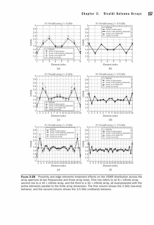
156 F r o n t i e r s i n a n t e n n a s : N e x t G e n e r a t i o n D e s i g n & e n g i n e e r i n g C h a p t e r 3 : V i v a l d i a n t e n n a a r r a y s 157
Figure 3-28 Proximity and edge elements treatment effects on the VSWR distribution across the array aperture at two frequencies and three array sizes. First row refers to an 8 × infinite array, second row to a 16 × infinite array, and the third to a 32 × infinite array, all dual-polarized with the active elements parallel to the finite array dimension. The first column shows the 2 GHz (low-end) behavior, and the second column shows the 3.5 GHz (midband) behavior.
5:1 Vivaldi array, f = 2 GHz
5:1 Vivaldi array, f = 2 GHz
3
InfiniteArray in free-spaceArray with dummy elementsArray over finite GPArray in cavity
InfiniteArray in free-spaceArray with dummy elementsArray over finite GPArray in cavity
InfiniteArray in free-spaceArray with dummy elementsArray over finite GPArray in cavity
InfiniteArray in free-spaceArray with dummy elementsArray over finite GPArray in cavity
2.82.62.42.2
21.8
1.61.41.2
11 2 3 4 5 6 7 8
16
2 4 6 8 10 12 1416 18 20 22 24 26 28 30 32 2 4 6 8 10 12 14 16 18 20 22 24 26 28 30 32
Element index1 2 3 4 5 6 7 8
Element index
Element index Element index
VSW
R
32.82.62.42.2
21.8
1.61.41.2
1
VSW
R
32.82.62.42.2
21.8
1.61.41.2
1
VSW
R
32.82.62.42.2
21.8
1.61.41.2
1
VSW
R
5:1 Vivaldi array, f = 3.5 GHz
5:1 Vivaldi array, f = 3.5 GHz
(a) (b)
InfiniteArray in free-spaceArray with dummy elementsArray over finite GPArray in cavity
1 2 3 4 5 6 7 8 9 10 11 12 13 14 15 16Element index
32.8
2.6
2.4
2.22
1.81.61.41.2
1
VSW
R
5:1 Vivaldi array, f = 3.5 GHz
(d)
5:1 Vivaldi array, f = 2 GHz
InfiniteArray in free-spaceArray with dummy elementsArray over finite GPArray in cavity
1 2 3 4 5 6 7 8 9 10 11 12 13 14 15Element index
32.82.62.42.2
21.8
1.61.41.2
1
VSW
R
(c)
(e) (f)

158 F r o n t i e r s i n a n t e n n a s : N e x t G e n e r a t i o n D e s i g n & e n g i n e e r i n g C h a p t e r 3 : V i v a l d i a n t e n n a a r r a y s 159
Figure 3-29 Effects of cavity enclosure on array active VSWR, when the finite array is in the H-plane. Plots show the VSWR distribution across the array “stick” (horizontal axis) vs. frequency (vertical axis) for a 16 × infinite dual-polarized Vivaldi array: (a) in free-space; (b) recessed in a cavity.
6
3
2.5
2
1.5
1
3
2.5
2
1.5
1
5.5
5
4.5
4
3.5
3
2.5
2
1.5
11 2 3 4 5 6 7 8 9 10 11 12 13 14 15 16 17
Element index1 2 3 4 5 6 7 8 9 10 11 12 13 14 15 16 17
Element index
VSWR, 5:1 Vivaldi array, array in free-space VSWR, 5:1 Vivaldi array, array in cavity
Freq
uen
cy [G
Hz]
6
5.5
5
4.5
4
3.5
3
2.5
2
1.5
1
Freq
uen
cy [G
Hz]
(a) (b)
Only the horizontally polarized elements are excited and the vertically polarized elements are terminated to 50 ohms. Fig. 3-30(a) depicts the 9 × 8 × 2 array while b and c corre-spond to the 17 × 16 × 2 and 33 × 32 × 2 arrays, respectively. As expected, the most severe truncation effects occur in the smallest size array. In all three cases, the edge elements in the E-plane and several elements in the interior of the arrays have the worst match-ing, indicating that they are most significantly affected by truncations. Specifically, ele-ments 5 rows and columns away from the array corners tend to have VSWR around 3.5, whereas the equivalent infinite array predicts VSWR approximately 2.5. In the 33 × 32 × 2 array there is further evidence of the periodic VSWR variation across the array that may be attributed to the interference of waves that are excited by edge and corner discon-tinuities and travel across the array. Truncation effects become less severe and affect differ-ent elements at higher frequencies as indicated by Fig. 3-31, which depicts the VSWR distributions of these arrays at 2 GHz.
To better demonstrate the standing-wave phenomena due to the edge and corner discontinuities, the Fourier transform of the deviation of the active reflection coefficient distribution from that of the infinite array is plotted in Fig. 3-32. This figure shows peaks at four locations near the edge of the visible space. These peaks represent surface waves prop-agating along grazing angles and have strong reactive components (the majority of the spec-trum is in invisible space). These waves are not present in infinite arrays and are launched from the edges. Ultimately these waves interact to generate the standing-wave pattern in Fig. 3-30. These have been observed under scattering excitation and idealized ports on dipole and patch arrays and have been termed array guided surface waves (AGSW) [65], [66].
To evaluate the accuracy of the infinite × finite array approximation in the previ-ous section, and to quantify corner truncations or edge-to-edge coupling interactions, the infinite × finite array results are compared with the finite array. The infinite × finite approach predicts an approximation of the active VSWR at the centerline of the finite array. Therefore, it provides no information about regions where the most severe finite array truncation effects appear, that is, 4–5 rows/columns away from the corners. A comparison of the VSWR at 2 GHz, across the finite array horizontal (E-plane) and

158 F r o n t i e r s i n a n t e n n a s : N e x t G e n e r a t i o n D e s i g n & e n g i n e e r i n g C h a p t e r 3 : V i v a l d i a n t e n n a a r r a y s 159
vertical (H-plane) centerlines with their respective infinite × finite array VSWR are given in Fig. 3-33 and Fig. 3-34, respectively. Overall, both results follow the same trends, except for the horizontal (E-plane) cut case of the smallest array (Fig. 3-33a), where the infinite × finite array overestimates the VSWR. Both infinite × finite and finite array results appear to fluctuate around the infinite array result, suggesting that a very well-matched infinite array would lead to acceptable VSWR across finite array center-lines, even in the presence of truncations.
Knowledge of the VSWR at each individual element in the array provides impor-tant information about regions and elements where T/R module failures due to large reflections or standing waves may occur. Considering the aperture as a whole, truncations mostly effect aperture mismatch efficiency, gain, and sidelobes.
Figure 3-30 VSWR distribution across the aperture of various size finite arrays at 1.5 GHz (only the excited, horizontal ports are plotted). (a) 9 × 8 × 2 dual-polarized array; (b) 17 × 16 × 2 dual-polarized array; (c) 33 × 32 × 2 dual-polarized array.
917
3230282624222018161412108642
2 4 6 8 10 12 14 16 18 20 22 24 26 28 30 32
4
3.5
3
2.5
2
1.5
1
16151413121110987654321
1 2 3 4 5 6 7 8 9 10 11 12 13 14 15 16
8
Ele
men
t ind
ex
Ele
men
t ind
ex
Ele
men
t ind
ex
Element index
Co-pol VSWR, 5:1 Vivaldi array,finite array, f = 1.5 GHz
Co-pol VSWR, 5:1 Vivaldi array,finite array, f = 1.5 GHz
Co-pol VSWR, 5:1 Vivaldi array,finite array, f = 1.5 GHz
Element index
Element index
7
6
5
4
3
2
11 2 3 4 5 6 7 8
(a) (b)
(c)
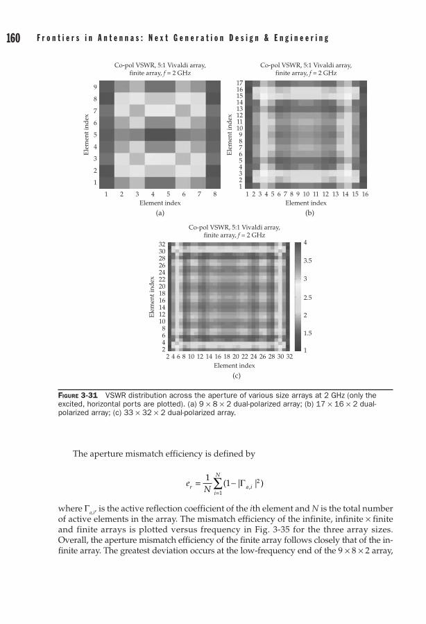
160 F r o n t i e r s i n a n t e n n a s : N e x t G e n e r a t i o n D e s i g n & e n g i n e e r i n g C h a p t e r 3 : V i v a l d i a n t e n n a a r r a y s 161
The aperture mismatch efficiency is defined by
eNr a i
i
N
= -=∑1
1 2
1
( | | ),Γ
where Γa,i, is the active reflection coefficient of the ith element and N is the total number of active elements in the array. The mismatch efficiency of the infinite, infinite × finite and finite arrays is plotted versus frequency in Fig. 3-35 for the three array sizes. Overall, the aperture mismatch efficiency of the finite array follows closely that of the in-finite array. The greatest deviation occurs at the low-frequency end of the 9 × 8 × 2 array,
Figure 3-31 VSWR distribution across the aperture of various size arrays at 2 GHz (only the excited, horizontal ports are plotted). (a) 9 × 8 × 2 dual-polarized array; (b) 17 × 16 × 2 dual-polarized array; (c) 33 × 32 × 2 dual-polarized array.
917
3230282624222018161412108642
16151413121110987654321
8
7
6
5
4
3
2
1
1 2 3 4Element index Element index
Element index
Co-pol VSWR, 5:1 Vivaldi array,finite array, f = 2 GHz
Co-pol VSWR, 5:1 Vivaldi array,finite array, f = 2 GHz
Co-pol VSWR, 5:1 Vivaldi array,finite array, f = 2 GHz
Ele
men
t ind
ex
Ele
men
t ind
ex
Ele
men
t ind
ex
5 6 7 8 1 2 3 4 5 6 7 8 9 10 11 12 13 14 15 16
2 4 6 8 10 12 14 16 18 20 22 24 26 28 30 32
(a) (b)
(c)
4
3.5
3
2.5
2
1.5
1

160 F r o n t i e r s i n a n t e n n a s : N e x t G e n e r a t i o n D e s i g n & e n g i n e e r i n g C h a p t e r 3 : V i v a l d i a n t e n n a a r r a y s 161
where the efficiency of the finite array is approximately 10% less than the infinite. This result agrees with conclusions drawn from Fig. 3-25, where the average VSWR follows quite closely the infinite array results.
Spatial variations of the matching introduced by truncations and diffractions from edges and corners affect the array far-field pattern. This is shown in Fig. 3-36 where pat-terns of 9 × 8 × 2 and 17 × 16 × 2 arrays are plotted at 2 GHz. Solid lines represent the far-field pattern of the actual finite array, whereas the dashed lines represent the radia-tion of infinite array (Floquet) element currents when arranged in the same periodic pattern as the finite array. As was mentioned in Section 3.1.6.3, this approximation produces similar results in the upper hemisphere as the traditional approach of pat-tern multiplication (infinite array element pattern times array factor) and is denoted as array factor approach in Figure legends. The array factor approximation follows well the actual finite array pattern. Some deviations between the two curves are ob-served at grazing and back angles and are attributed to truncations, because the array factor plot includes the infinite array mutual coupling, but ignores truncation effects. Array factor predictions have lower sidelobe level at far sidelobes and well-defined nulls between them. In both cases, the finite array results predict slightly higher maximum
Figure 3-32 Finite array guided surface waves lanched from the edge discontinuities. The plot shows the Fourier transform of the deviation of the active reflection coefficient distribution of a 17 × 16 × 2 dual-polarized Vivaldi array from the infinite array, FTGa-Ginf , at 1.5 GHz. Four peaks, near the edges of the visible space, represent four interfering array guided surface waves that form a standing-wave pattern.
–3
FT (γa – γinf), 17×16×2 Vivaldi array, broadside scan f = 1.5 GHz
–2.5
–2
–1.5
–1
–0.5
0
0.5
1
1.5
2
2.5
3
–3 –2.5 –1.5 –0.5–40
–35
–30
–25
–20
–15
–10
–5
0
0.5 1.5 2.5 3210–1–2
sinθ
sin
φ
sinθ cosφ

162 F r o n t i e r s i n a n t e n n a s : N e x t G e n e r a t i o n D e s i g n & e n g i n e e r i n g C h a p t e r 3 : V i v a l d i a n t e n n a a r r a y s 163
directivity (≈0.4 dB for the smallest array). The effects described here for broadside excitation become more pronounced at scan angles and at lower frequencies.
3.2.4.2 Array ShapeThis section shows how the arrangement of edge elements and the finite array shape can affect the reflection coefficient distribution across the aperture. The layouts of the array cases considered here are shown in Fig. 3-37, where each colored rectangle repre-sents the magnitude of the active reflection coefficient of each Vivaldi array element (horizontal tiles represent horizontal elements and vertical tiles represent vertical elements). In Fig. 3-37a and d the full egg crate configuration is maintained through-out the array, whereas in Fig. 3-37b and e, the egg crates at edge rows and columns are open. The figure also shows two rhombic shaped arrays, where the array edges are 45° from the horizontal or vertical polarized elements. In Figs. 3-37a through c, the size of the
Figure 3-33 Comparison between finite array VSWR at the E-plane centerline with the corresponding infinite × finite array VSWR. (a) 9 × 8 × 2 array; (b) 17 × 16 × 2 array; (c) 33 × 32 × 2 array.
32.82.62.42.2
21.81.61.41.2
11 2 3 4 5 6 7 8
Element index
5:1 Vivaldi array, f = 2 GHz, E-plane cut 5:1 Vivaldi array, f = 2 GHz, E-plane cut
VSW
R
32.82.62.42.2
21.81.61.41.2
1
VSW
R
Element index1 2 3 4 5 6 7 8 9 10 11 12 13 1415 16
(a) (b)
Infinite × infiniteInfinite × finiteFinite × finite
Infinite × infiniteInfinite × finiteFinite × finite
5:1 Vivaldi array, f = 2 GHz, E-plane cut
Element index
32.82.62.42.2
21.81.61.41.2
1
VSW
R
2 4 6 8 1012 14 1618 20 22 2426 28 30 32
(c)
Infinite × infiniteInfinite × finiteFinite × finite
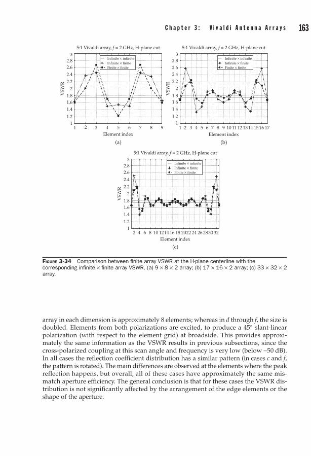
162 F r o n t i e r s i n a n t e n n a s : N e x t G e n e r a t i o n D e s i g n & e n g i n e e r i n g C h a p t e r 3 : V i v a l d i a n t e n n a a r r a y s 163
array in each dimension is approximately 8 elements; whereas in d through f, the size is doubled. Elements from both polarizations are excited, to produce a 45° slant-linear polarization (with respect to the element grid) at broadside. This provides approxi-mately the same information as the VSWR results in previous subsections, since the cross-polarized coupling at this scan angle and frequency is very low (below -50 dB). In all cases the reflection coefficient distribution has a similar pattern (in cases c and f, the pattern is rotated). The main differences are observed at the elements where the peak reflection happens, but overall, all of these cases have approximately the same mis-match aperture efficiency. The general conclusion is that for these cases the VSWR dis-tribution is not significantly affected by the arrangement of the edge elements or the shape of the aperture.
Figure 3-34 Comparison between finite array VSWR at the H-plane centerline with the corresponding infinite × finite array VSWR. (a) 9 × 8 × 2 array; (b) 17 × 16 × 2 array; (c) 33 × 32 × 2 array.
5:1 Vivaldi array, f = 2 GHz, H-plane cut 5:1 Vivaldi array, f = 2 GHz, H-plane cut
5:1 Vivaldi array, f = 2 GHz, H-plane cut
32.82.6
2.42.2
2
1.81.61.4
1.21
VSW
R
32.82.6
2.42.2
2
1.81.61.4
1.21
VSW
R
32.82.62.42.2
2
1.81.61.4
1.21
VSW
R
Infinite × infiniteInfinite × finiteFinite × finite
Infinite × infiniteInfinite × finiteFinite × finite
Infinite × infiniteInfinite × finiteFinite × finite
1 2 3 4 5 6 7 8 9Element index
(a)Element index
1 2 3 4 5 6 7 8 9 10 11 12 1314 1516 17
(b)
Element index2 4 6 8 10 1214 16 18 2022 24 26 2830 32
(c)

164 F r o n t i e r s i n a n t e n n a s : N e x t G e n e r a t i o n D e s i g n & e n g i n e e r i n g C h a p t e r 3 : V i v a l d i a n t e n n a a r r a y s 165
Figure 3-35 Aperture mismatch efficiency versus frequency for infinite, infinite × finite and finite × finite Vivaldi arrays of various sizes. (a) 9 × 8 × 2 dual-polarized array; (b) 17 × 16 × 2 dual-polarized array; (c) 33 × 32 × 2 dual-polarized array.
5:1 Dual-pol. Vivaldi 9×8×2 arrayin free-space
1 1.5 2 2.5 3 3.5 4 4.5 5 5.5 1 1.5 2 2.5 3 3.5 4 4.5 5 5.5
1 1.5 2 2.5 3 3.5 4 4.5Freq [GHz]
Freq [GHz]Freq [GHz]
5 5.5
5:1 Dual-pol. Vivaldi 17×16×2 arrayin free-space
5:1 Dual-pol. Vivaldi 33×32×2 arrayin free-space
e r =
(1 –
|Γa|2 )[
%]
e r =
(1 –
|Γa|2 )[
%]
e r =
(1 –
|Γa|2 )[
%]
Infinite × infiniteInfinite × finiteFinite × finite
Infinite × infiniteInfinite × finiteFinite × finite
Infinite × infiniteInfinite × finiteFinite × finite
100
95
90
85
80
75
70
100
95
90
85
80
75
70
100
95
90
85
80
75
70
(a) (b)
(c)
Figure 3-36 Effects of truncations on far-field pattern under broadside excitation at 2 GHz. (a) 9 × 8 × 2 dual-polarized array; (b) 17 × 16 × 2 dual-polarized array. The solid line shows the actual finite array radiation pattern and the dashed line shows patterns obtained from the infinite array (Floquet) element currents arranged in the same array size (approximately the same as array factor × infinite array element pattern).
5:1 Vivaldi array, array in free-space, freq = 2 GHz 5:1 Vivaldi array, array in free-space, freq = 2 GHz
Array factorFinite × finite
Array factorFinite × finite
(a)
Dir
ecti
vity
[dB
]
Dir
ecti
vity
[dB
]
(b)
30
25
20
15
10
5
0
–5
–10
–15
–20
–25
–30
30
25
20
15
10
5
0
–5
–10
–15
–20
–25
–30–180 –150 –120 –90 –60 –30 0 30 60 90 120 150 180 –180 –150 –120 –90 –60 –30 0 30 60 90 120 150 180
θ [deg] θ [deg]
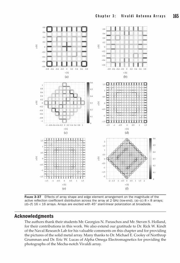
164 F r o n t i e r s i n a n t e n n a s : N e x t G e n e r a t i o n D e s i g n & e n g i n e e r i n g C h a p t e r 3 : V i v a l d i a n t e n n a a r r a y s 165
AcknowledgmentsThe authors thank their students Mr. Georgios N. Paraschos and Mr. Steven S. Holland, for their contributions in this work. We also extend our gratitude to Dr. Rick W. Kindt of the Naval Research Lab for his valuable comments on this chapter and for providing the pictures of the solid metal array. Many thanks to Dr. Michael E. Cooley of Northrop Grumman and Dr. Eric W. Lucas of Alpha Omega Electromagnetics for providing the photographs of the Mecha-notch Vivaldi array.
Figure 3-37 Effects of array shape and edge element arrangement on the magnitude of the active reflection coefficient distribution across the array at 2 GHz (low-end). (a)–(c) 8 × 8 arrays; (d)–(f) 16 × 16 arrays. Arrays are excited with 45° slant-linear polarization at broadside.
0.8
0.6
0.4
0.2
0
–0.2
–0.4
–0.6
–0.8–0.8 –0.6 –0.4 –0.2 0 0.2 0.4 0.6 0.8
y [λ
]
x [λ]
(a) (b)
(c) (d)
(e) (f)
0
0.8
0.6
0.4
0.2
–0.2
–0.4
–0.6
–0.8
y [λ
]
–0.8 –0.6 –0.4 –0.2 0 0.2 0.4 0.6 0.8
x [λ]
0
0.8
1
0.6
0.4
0.2
–0.2
–0.4
–0.6
–0.8
–1
y [λ
]
–0.8–1 –0.6–0.4–0.2 0 0.2 0.4 0.6 0.8 1
x [λ]
0.6
0.5
0.4
0.3
0.2
0.1
0
1.5
1
0.5
0
–0.5
–1
–1.5
–1.5 –1 –0.5 0 0.5 1 1.5
y [λ
]
x [λ]
1.5
2
1
0.5
0
–0.5
–1
–1.5
–2
y [λ
]
0.6
0.5
0.4
0.3
0.2
0.1
0–1.5–2 –1 –0.5 0 0.5 1 1.5 2
x [λ]
–1.5 –1 –0.5 0 0.5 1 1.5
x [λ]
1.5
1
0.5
0
–0.5
–1
–1.5
y [λ
]

166 F r o n t i e r s i n a n t e n n a s : N e x t G e n e r a t i o n D e s i g n & e n g i n e e r i n g C h a p t e r 3 : V i v a l d i a n t e n n a a r r a y s 167
ReferencesL. R. Lewis, M. Fassett, and J. Hunt, “A broadband stripline array element,” [1] IEEE Antennas and Propagat. Symp. Digest, pp. 335–337, Atlanta, 1974.B. A. Munk, [2] Finite Antenna Arrays and FSS. John Wiley and Sons, 2003.P. Friederich, L. Pringle, L. Fountain, and P. Harms, “A new class of broadband planar apertures,” [3] in Proceedings of the 2001 in Antenna Applications Symposium, (Allerton Park, Monticello, IL), pp. 561–587, Sep. 2001.J. J. Lee, S. Livingston, and R. Koenig, “A low-profile wide-band (5:1) dual-pol array,” [4] IEEE Antenna Wireless Propag. Lett., vol. 2, pp. 46–49, 2003.J. J. Lee, S. Livingston, R. Koenig, D. Nagata, and L. L. Lai, “Compact light weight UHF arrays using [5] long slot apertures,” IEEE Trans. Antennas and Propag., vol. 54, pp. 2009–2015, Jul. 2006.M. W. Elsallal, and D. H. Schaubert, “Reduced-height array of BAVA with greater than octave [6] bandwidth,” 2005 Antenna Applications Symposium, pp. 226–242, 21–23 Sept. 2005.S. S. Holland, and M. N. Vouvakis, “A 7-21 GHz planar ultrawideband modular array,” in [7] 2010 IEEE Antennas and Prop. Soc. Intern. Symposium, Jul. 2010.P. J. Gibson, “The Vivaldi Aerial,” [8] 9th Eur. Microw. Conf., pp. 101–105, Brighton, UK, 1979.M. J. Povinelli, and J. A. Johnson, “Design and performance of wideband dual polarized stripline [9] notch arrays,” IEEE Antennas and Propagat. Symp. Digest, pp. 200–203, Syracuse, 1988.P. S. Simon, K. McInturff, R. W. Jobsky, and D. L. Johnson, “Full-Wave analysis of an infinite, planar [10] array of linearly polarized, stripline-fed, tapered notch elements,” IEEE Antennas and Propagat. Symp. Digest, pp. 334–337, London, Ont., 1991.D. H. Schaubert, J. A. Aas, M. E. Cooley, and N. E. Buris, “Moment method analysis of infinite strip-[11] line-fed tapered slot antenna arrays with a ground plane,” IEEE Trans. Antennas and Propagat., vol. 42, no. 8, pp. 1161–1166, Aug. 1994.D. T. McGrath, and V. P. Pyati, “Phased array antenna analysis with the hybrid finite element [12] method,” IEEE Trans. Antennas and Propagat., vol. 42, no. 12, pp. 1625–1630, Dec. 1994.E. W. Lucas, and T. P. Fontana, “A 3-D hybrid finite element/boundary element method for the [13] unified radiation and scattering analysis of general infinite periodic arrays,” IEEE Trans. Antennas and Propagat., vol. 43, no. 2, pp. 145–153, Feb. 1995.J. H. Pozgay, “A wideband sub-array radiator for advanced avionics applications,” Presented at the [14] 1992 Antenna Applications Symposium, Monticello, IL.J. Shin, and D. H. Schaubert, “A parameter study of stripline-fed Vivaldi notch-antenna arrays,” [15] IEEE Trans. on Antennas and Propag, vol. 47, no. 5, pp. 879–886, May 1999.T-H. Chio, and D. H. Schaubert, “Parameter study and design of wideband, widescan dual-polarized [16] tapered slot antenna arrays,” IEEE Trans. on Antennas and Propag, vol. 48, no. 6, pp. 879–886, June 2000.N. Schuneman, J. Irion, and R. Hodges, “Decade bandwidth tapered notch antenna array ele-[17] ment,” Proceedings of the 2001 Antenna Applications Symposium, (Allerton Park, Monticello, IL), pp. 280–294, Sep. 2001. K. Trott, B. Cummings, R. Cavener, M. Deluca, J. Biondi, and T. Sikina, “Wideband phased array [18] radiator,” Proc. IEEE Int. Symp. on Phased Array Systems and Technology, pp. 383–386, 2003.M. B. Davis, “Wide-band L-band corporate fed antenna for space based radars,” U. S. Patent [19] 5,227,808, Jul. 1993.C. Hemmi, R. T. Dover, F. German, and A. Vespa, “Multifunction wide-band array design,” [20] IEEE Trans. Antennas Propag., vol. 47, no. 3, pp. 425–431, March 1999.D. H. Schaubert, A. O. Boryssenko, A. van Ardenne, J. G. Bij de Vaate, and C. Craeye, “The square [21] kilometer array (SKA) antenna,” Proc. IEEE Int. Symp. on Phased Array Systems and Technology, pp. 351–358, 14–17 Oct. 2003.R. Maaskant, M. Popova, and R. van den Brink, “Towards the design of a low-cost wideband [22] demonstrator tile for the SKA,” First European Conference on Antennas and Propagation, EuCAP, pp. 1–4, 6–10 Nov. 2006.M. V. Ivashina, M. Kehn, P.-S. Kildal, and R. Maaskant, “Decoupling efficiency of a wideband Vivaldi [23] focal plane array feeding a reflector antenna,” IEEE Trans. Antennas and Propag., vol. 57, pp. 373–382, Feb. 2009.Y. Yang, C. Zhang, and A. E. Fathy, “Development and implementation of ultra-wideband see-[24] through-wall imaging system based on sampling oscilloscope,” IEEE Antennas Wireless Propag. Lett., vol. 7, pp. 465–468, 2008.S. Balling, M. Hein, M. Hennhofer, G. Sommerkorn, R. Stephan, and R. Thoma, “Broadband dual [25] polarized antenna arrays for mobile communication applications,” 33rd European Microwave Conference, vol. 3, pp. 927–930, 7–9 Oct. 2003.

166 F r o n t i e r s i n a n t e n n a s : N e x t G e n e r a t i o n D e s i g n & e n g i n e e r i n g C h a p t e r 3 : V i v a l d i a n t e n n a a r r a y s 167
R. A. York, and Z. B. Popovic, eds., [26] Active and Quasi-Optical Arrays for solid-State Power Combining. Wiley Series in Microwave and Optical Engineering, 1997.H. Holter, T.-H. Chio, and D. H. Schaubert, “Elimination of impedance anomalies in single- and [27] dual-polarized endfire tapered slot phased arrays,” IEEE Trans. Antennas and Propag., vol. 48, pp. 122–124, Jan. 2000.N. Marchand, “Transmission line conversion transformers,” [28] Electronics, vol. 17, pp. 142–145, Dec. 1944.J. B. Knorr, “Slot-line transitions,” [29] IEEE Trans. Micro. Theory Tech., vol. 22, no. 5, pp. 548–554, 1974.B. A. Munk, “Chapter 23— Baluns,” in [30] Antennas (J. D. Kraus, and R. J. Marhefka, eds.), New York McGraw-Hill, 2002.B. Schiek, and J. Kohler, “An improved microstrip-to-microslot transition,” [31] IEEE Trans. Micro. Theory Tech., vol. 24, pp. 231–233, Apr. 1976.M. Kragalott, W. R. Pickles, and M. S. Kluskens, “Design of a 5:1 bandwidth stripline notch array [32] from FDTD analysis,” IEEE Trans. Antennas Propag., vol. 48, no. 11, pp. 1733–1741, Nov. 2000.V. Trifunovic, and B. Jokanovic, “Review of printed Marchand and double Y baluns: characteristics [33] and application,” IEEE Trans. Micro. Theory Tech., vol. 42, pp. 1454–1462, Aug. 1994.A. Ellgardt, “A scan blindness model for single-polarized tapered-slot arrays in triangular grids,” [34] IEEE Trans. Antennas and Propag., vol. 56, pp. 2937–2942, Sep. 2008.A. Ellgardt, and A. Wikstrom, “A single polarized triangular grid tapered-slot array antenna,” [35] IEEE Trans. Antennas and Propag., vol. 57, pp. 2599–2607, Sep. 2009.Y. H. Choung, “Wideband double-slot cross-notch antenna,” in [36] 2001 IEEE Antennas and Propagation Society International Symposium, vol. 2, pp. 448–451, doi: 10.1109/APS.2001.959758, 2001.W. Mohuchy, P. Beyerle, and A. MacFarland, “4.5:1 bandwidth microstrip notch array measured [37] performance,” in 2001 IEEE Antennas and Propagation Society International Symposium, vol. 2, pp. 444–447, doi:10.1109/APS.2001.959757, 2001.K. D. Trott, J. P. Biondi, R. J. Cavener, R. V. Cummings, J. M. McGuinnis, T. V. Sikina, E. A. Yurteri, [38] and F. Beltran, “Wideband phased array radiator.” U. S. Pattent 7,180,457 B2, Feb. 2007.W. Pickles, J. Rao, D. Patel, and R. Mital, “Coincident phase center ultra wideband array of dual [39] polarized flared notch elements,” in 2007 IEEE Antennas and Propagation Society International Symposium, pp. 4421–4424, June 2007.T. P. Fontana, “Hexagonal dual-pol notch array architecture having a triangular grid and concentric [40] phase centers.” U. S. Patent 7, 333, 058 B2, Feb. 2008.D. H. Schaubert, “A gap-induced element resonance in single-polarized arrays of notch antennas,” [41] in 1994 IEEE Intern. Symposium Antennas and Prop. Soc, vol. 2, pp. 1264–1267, Jul. 1994.R. Kindt, and R. Pickles, “12-to-1 bandwidth all-metal Vivaldi array element,” in [42] 2009 IEEE Antennas and Prop. Soc. Intern. Symposium, pp. 1–4 doi:10.1109/APS.2009.5171599, Jun. 2009.R. W. Kindt, and W. R. Pickles, “All-Metal flared-notch array radiator for ultrawideband applica-[43] tions,” NRL Memorandum Report, NRL MR 5310, March 25th 2010.R. W. Kindt, and W. R. Pickles, “Ultra-wideband all-metal flared-notch array radiator,” [44] IEEE Trans. Antennas and Propag., vol. 58, no. 11, pp. 3568-3575, Nov. 2010.H. Holter, “Dual-polarized broadband array antenna with BOR-elements, mechanical design and [45] measurements,” IEEE Trans. Antennas Propag., vol. 55, no. 2, pp. 305–312, Feb. 2007.E. W. Lucas, “Notch radiator elements.” U. S. Patent 5,194,875, Mar. 1993.[46] N. Amitay, V. Galindo, and C.-P. Wu, [47] Theory and Analysis of Phased Array Antennas. New York, NY: Wiley Interscience, 1972.A. C. Ludwig, “The definition of cross polarization,” [48] IEEE Trans. Antennas and Propag., vol. 21, pp. 116–119, Jan. 1973.R. Mittra, “A look at some challenging problems in computational electromagnetics,” [49] IEEE Ant. Propag. Mag., vol. 46, no. 7, pp. 18–32, 2004.M. G. Floquet, “Sur les equations differentielles lineaires a cofficients periodiques,” [50] Annale Ecole Normale Superieut, vol. pp. 47–88, 1883.M. N. Vouvakis, K. Zhao, and J.-F. Lee, “Finite-element analysis of infinite periodic structures with [51] nonmatching triangulations,” IEEE Trans. Magn., vol. 42, no. 4, pp. 691–694, 2006.H. Holter, and H. Steyskal, “Infinite phased-array analysis using FDTD periodic boundary [52] conditions-pulse scanning in oblique directions,” IEEE Trans. Antennas and Propagat., vol. 47, pp. 1508–1514, Oct. 1999.L. E. R. Petersson, and J.-M. Jin, “A three-dimensional time-domain finite-element formulation for [53] periodic structures,” IEEE Trans. Antennas and Propag., vol. 54, pp. 12–19, Jan. 2006.G. N. Paraschos, and M. N. Vouvakis, “Stability analysis of some non-conforming FETI domain [54] decomposition methods for electromagnetic problems,” in 2008 IEEE Antennas and Prop. Soc. Intern. Symposium, pp. 1–4, doi = 10.1109/APS.2008.4619093, 2009.

168 F r o n t i e r s i n a n t e n n a s : N e x t G e n e r a t i o n D e s i g n & e n g i n e e r i n g
G. N. Paraschos, and M. N. Vouvakis, “A design methodology for finite phased arrays and [55] repetitive structures,” in 2009 IEEE Antennas and Prop. Soc. Intern. Symposium, pp. 1–4, doi:10.1109/APS.2009.5171582, 2009.J.-M. Jin, Z. Lou, Y.-J. Li, N. Riley, and D. Riley, “Finite element analysis of complex antennas and [56] arrays,” IEEE Trans. Antennas and Propag., vol. 56, pp. 2222–2240, Aug. 2008.S. C. Lee, M. Vouvakis, and J.-F. Lee, “A non-overlapping domain decomposition method with [57] non-matching grids for modeling large finite antenna arrays,” Journal of Computational Physics, vol. 203, no. 1, pp. 1–21, Feb. 2005.M. N. Vouvakis, [58] A Non-Conformal Domain Decomposition Method for Solving Large Electromagnetic Wave Problems. PhD thesis, Electrical & Computer Engineering, The Ohio State University, Columbus, 2005.R. W. Kindt, and J. L. Volakis, “Array decomposition-fast multipole method for finite array [59] analysis,” Radio Science, vol. 39, no. 2, p. 16, April 2004.R. Maaskant, R. Mittra, and A. Tijhuis, “Fast analysis of large antenna arrays using the charac-[60] teristic basis function method and the adaptive cross approximation algorithm,” IEEE Trans. Antennas Propag., vol. 56, no. 11, pp. 3440–3451, Nov. 2008.P. Pirinoli, L. Matekovits, F. Vipiana, G. Vecchi, and M. Orefice, “Multi-grid SFX-MR approach for the [61] analysis of large arrays,” 18th International Conference on Applied Electromagnetics and Communications (ICECom), pp. 1–4, 12–14 Oct. 2005.D. J. Bekers, S. J. L. van Eijndhoven, A. A. F. van de Ven, P.-P. Borsboom, and A. G. Tijhuis, [62] “Eigencurrent analysis of resonant behavior in finite antenna arrays,” IEEE Trans. Microw. Theory Tech., vol. 54, no. 6, pp. 2821–2829, June 2006.D. K. Sun, Z. Cendes, and J.-F. Lee, “Adaptive mesh refinement, h-version, for solving multiport [63] microwave devices in three dimensions,” IEEE Trans. Magn., vol. 36, pp. 1596–1599, Jul. 2000.H. Holter, and H. Steyskal, “On the size requirement for finite phased-array models,” [64] IEEE Trans. Antennas Propag., vol. 50, pp. 836–840, Jun. 2002.D. S. Janning, and B. A. Munk, “Effects of surface waves on the currents of truncated periodic arrays,” [65] IEEE Trans. AntennasPropag., vol. 50, pp. 1254–1265, Sep. 2002.O. A. Civi, and P. H. Pathak, “Array guided surface waves on a finite planar arrays of dipoles with [66] or without a grounded substrate,” IEEE Trans. Antennas and Propag., vol. 54, pp. 2244–2252, Aug. 2006.

CHAPTER 4Artificial Magnetic Conductors/High-
Impedance Surfaces
Victor C. Sanchez and Jodie M. Bell
4.1 IntroductionAn artificial magnetic conductor (AMC) sometimes referred-to as a high-impedance surface (HIS)—is a lossless reactive surface—typically realized as a printed circuit board. The basic construct, often called the Sievenpiper “mushroom” structure [1], consists of low-profile metallic inclusions placed periodically on a grounded dielectric slab as shown in Fig. 4-1. The construct can be viewed as having a capacitive “FSS” layer above a grounded “spacer” layer, with each conducting patch in the FSS layer connected to ground through a metal via.
AMC structures have gained significant attention in recent years mainly due to their potential as backing structures for low-profile antennas [2] – [4]. It is specifically this application that highlights the two important properties of the AMC—namely, the ability to present high impedance to a localized source or plane wave looking down into the structure as well as a surface-wave band-gap that prohibits the transverse propagation of energy along the surface.
AMC structures are usually designed such that both of the above properties exist over the same frequency band, but there are some applications where only one or the other property is required. This is true for many HIS realizations, which do not necessarily exhibit the surface wave band-gap feature at all [5]. The term EBG (electromagnetic band-gap structure) is also often used in the open literature to describe the constructs discussed in this chapter. This can lead to some confusion as the term EBG also applies to a broader category of structures where the band-gap is due to Bragg scattering from a periodic arrangement of dielectric inclusions spaced one-half guide wavelength apart.
169

170 F r o n t i e r s i n A n t e n n a s : N e x t G e n e r a t i o n D e s i g n & E n g i n e e r i n g C h a p t e r 4 : A r t i f i c i a l M a g n e t i c C o n d u c t o r s / H i g h - I m p e d a n c e S u r f a c e s 171
In fact, EBGs can be viewed as the RF-frequency implementation of the optical structures known as photonic band-gap structures (PBGs), originally named from the forbidden propagation bands exhibited by certain semiconductor and crystal materials at optical frequencies [6], [7]. Because of the half-wavelength periodicity, the dispersion diagrams for PBGs and some EBGs tend to have a strong dependence on direction of propagation, and it is not possible to successfully represent the material as a uniform homogenized effective material.
In this chapter, we adopt the term AMC to describe structures with metallic inclusions having periodicities much smaller than a free space wavelength, and that exhibit both the high-surface impedance and surface-wave band-gap properties. We will review analysis techniques based on homogenized effective media models [8], [9], and simpler LC and transmission line models [1], [10], and discuss a variety of new and novel AMC constructs with more-specialized applications that have been developed in recent years. However, we begin by discussing the background that led to the development of the AMC and the recent history leading to the current state of the art.
4.2 Historical BackgroundThe building blocks for the development of the AMC were formed throughout the latter half of the last century. There has long been a need for conductive antenna backing structures due to a need for isolation-from and/or integration-into conducting installation environments. In order to avoid shorting out transverse currents, sufficiently high impedance is necessary looking back into the ground. Historically this has been achieved by either spacing the radiating element one quarter of a free space wavelength above the ground, loading the volume behind the radiator with dielectric and/or lossy material, or simply putting the element close to the ground and accepting the degradation in VSWR performance [11] – [13]. The acceptability of each of these approaches is application dependent, with performance trade-offs dictated by operating frequency and bandwidth, available volume, and other RF and mechanical antenna performance metrics.
For a horizontal dipole over a lossless substrate, the AMC allows a reduction in the total physical spacing required to achieve a good impedance match—at the expense of instantaneous bandwidth. This same impedance match can also be achieved using a grounded high-dielectric substrate with quarter-wave electrical thickness. However, such a substrate would guide surface waves in the transverse direction, reducing
Figure 4-1 Cross-sectional and three-dimensional perspective of the Sievenpiper AMC
CapacitiveFSS Layer
Low PermittivitySpacer Layer
Metal Vias Metal Backplane Metal Vias

170 F r o n t i e r s i n A n t e n n a s : N e x t G e n e r a t i o n D e s i g n & E n g i n e e r i n g C h a p t e r 4 : A r t i f i c i a l M a g n e t i c C o n d u c t o r s / H i g h - I m p e d a n c e S u r f a c e s 171
efficiency for the single element case and adversely affecting scan in the array case [14], [15]. The surface-wave band-gap associated with the AMC mitigates this effect, enhancing its suitability for low-profile antenna applications.
The building blocks for the development of the band-gap feature have also been in place for some time. Corrugated surfaces have been used as chokes to reduce coupling or as planar leaky-wave antennas since the 1950s [16], [17]. Further, the “bed of nails” structure that was studied by King and Park [18] was a notable precursor to the AMC. This structure inhibited TM surface-wave propagation using conducting vias protruding from a metal ground plane (essentially the AMC without the capacitive metal patches).
The first demonstrated, electrically-thin, HIS was published in 1993 by Rodger Walser et. al. [19]. A parquet surface was proposed where each cell in the parquet pattern is a two-dimensional structure comprised of planar strips connected to a backside ground plane using conductive vias in the form of parallel walls. Reflection phase of this HIS was measured and shown to have a zero phase resonance. In this paper, Walser also proposed an electronically tunable HIS by varying the effective capacitance between parallel strips of the FSS. However, surface-wave properties were not investigated.
In 1999, Sievenpiper, Zhang, and Yablonovitch at UCLA introduced the first true AMC to the microwave and antenna community. This first mushroom-like structure was designed to produce a near-zero-degree reflection phase while at the same time provid-ing a forbidden frequency band for surface-wave propagation. Since then, there has been a large body of work published on many variations of this basic construct to varying ends. Much of the work done soon after the initial publication was in the area of un-derstanding the fundamental mechanisms and extending the bandwidth through minor permutations to the original geometry. Some of this work was documented in the IEEE Transactions on Antennas and Propagation special issue on AMCs in January, 2005. Other authors have generated multiband structures through multiple layers or more complex unit cells [20], [21]. Yet others have used the basic construct for other purposes—such as reducing coupling in arrays to improve scan performance [22] or border treatments to improve pattern performance through control of interaction with the installation environment [23], [24]. Still others have focused on exciting the AMC surface itself to form and scan a beam through control of leaky-wave modes [25]. Many of these more recent developments are described in detail throughout the rest of this chapter, following a discussion on AMC theory and analysis.
4.3 Fundamental Theory, Analysis, and SimulationThe impedance and surface-wave properties of the AMC can be derived using a variety of techniques, including simple circuit models, effective media representation, and full-wave simulation of the unit cell or entire finite radiating structure using commercially available computational electromagnetic (CEM) tools. This section provides an overview of each of these methods.
4.3.1 Equivalent Circuit ModelFor plane waves at normal incidence, an AMC may be understood as an electrically short length of shorted transmission line with a shunt capacitance placed at the reference plane of the outer surface. This is shown in Fig. 4-2. The electrically short length of shorted transmission line can be approximated by an inductor. Thus, the equivalent
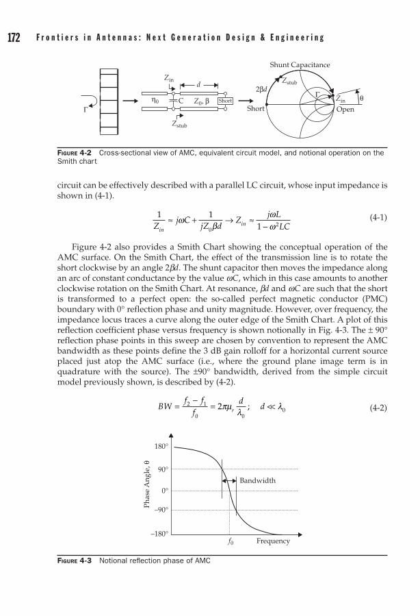
172 F r o n t i e r s i n A n t e n n a s : N e x t G e n e r a t i o n D e s i g n & E n g i n e e r i n g C h a p t e r 4 : A r t i f i c i a l M a g n e t i c C o n d u c t o r s / H i g h - I m p e d a n c e S u r f a c e s 173
circuit can be effectively described with a parallel LC circuit, whose input impedance is shown in (4-1).
1 110
2Zj C
jZ dZ
j LLCin
in≈ + → ≈-
ωβ
ωω
(4-1)
Figure 4-2 also provides a Smith Chart showing the conceptual operation of the AMC surface. On the Smith Chart, the effect of the transmission line is to rotate the short clockwise by an angle 2bd. The shunt capacitor then moves the impedance along an arc of constant conductance by the value wC, which in this case amounts to another clockwise rotation on the Smith Chart. At resonance, bd and wC are such that the short is transformed to a perfect open: the so-called perfect magnetic conductor (PMC) boundary with 0° reflection phase and unity magnitude. However, over frequency, the impedance locus traces a curve along the outer edge of the Smith Chart. A plot of this reflection coefficient phase versus frequency is shown notionally in Fig. 4-3. The ± 90° reflection phase points in this sweep are chosen by convention to represent the AMC bandwidth as these points define the 3 dB gain rolloff for a horizontal current source placed just atop the AMC surface (i.e., where the ground plane image term is in quadrature with the source). The ±90° bandwidth, derived from the simple circuit model previously shown, is described by (4-2).
BWf f
fd
dr=-
= <<2 1
0 002πµ
λλ; (4-2)
Figure 4-2 Cross-sectional view of AMC, equivalent circuit model, and notional operation on the Smith chart
Zin
Zin
Zstub
Zstub
Open
2βd
Z0, βη0 θΓ
Γ
Shunt Capacitance
ShortShort
d
C
Figure 4-3 Notional reflection phase of AMC
180°
–180°f0 Frequency
Bandwidth90°
–90°
0°
Phas
e A
ngle
, θ
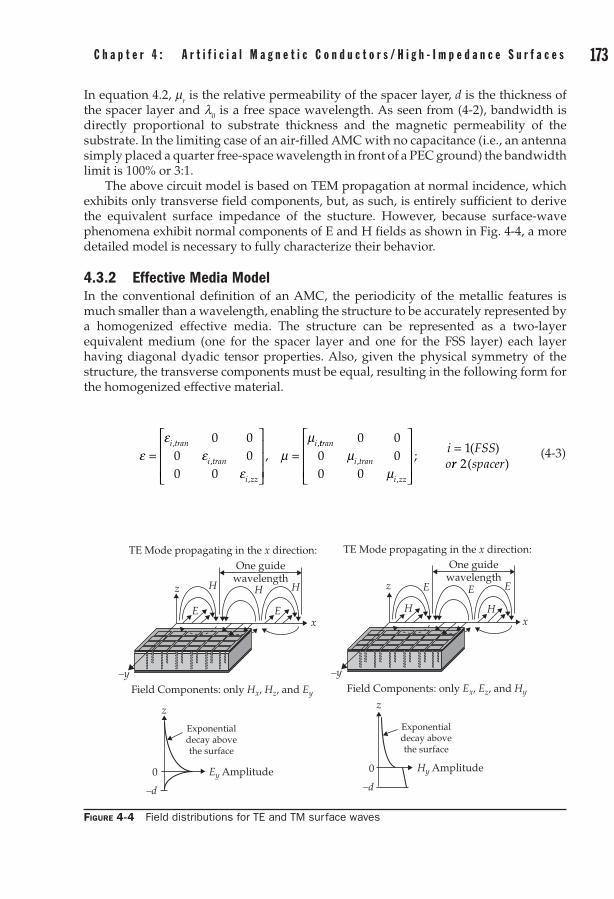
172 F r o n t i e r s i n A n t e n n a s : N e x t G e n e r a t i o n D e s i g n & E n g i n e e r i n g C h a p t e r 4 : A r t i f i c i a l M a g n e t i c C o n d u c t o r s / H i g h - I m p e d a n c e S u r f a c e s 173
In equation 4.2, mr is the relative permeability of the spacer layer, d is the thickness of the spacer layer and l0 is a free space wavelength. As seen from (4-2), bandwidth is directly proportional to substrate thickness and the magnetic permeability of the substrate. In the limiting case of an air-filled AMC with no capacitance (i.e., an antenna simply placed a quarter free-space wavelength in front of a PEC ground) the bandwidth limit is 100% or 3:1.
The above circuit model is based on TEM propagation at normal incidence, which exhibits only transverse field components, but, as such, is entirely sufficient to derive the equivalent surface impedance of the stucture. However, because surface-wave phenomena exhibit normal components of E and H fields as shown in Fig. 4-4, a more detailed model is necessary to fully characterize their behavior.
4.3.2 Effective Media ModelIn the conventional definition of an AMC, the periodicity of the metallic features is much smaller than a wavelength, enabling the structure to be accurately represented by a homogenized effective media. The structure can be represented as a two-layer equivalent medium (one for the spacer layer and one for the FSS layer) each layer having diagonal dyadic tensor properties. Also, given the physical symmetry of the structure, the transverse components must be equal, resulting in the following form for the homogenized effective material.
εε
εε
µµ
=
=i tran
i tran
i zz
i,
,
,
,
,0 0
0 00 0
ttran
i tran
i zz
i FSSo
0 00 00 0
1µµ
,
,
;( )
=rr spacer2( )
(4-3)
Figure 4-4 Field distributions for TE and TM surface waves
TE Mode propagating in the x direction: TE Mode propagating in the x direction:
One guidewavelength
One guidewavelength
z z
z z
Ey Amplitude Hy Amplitude0 0
–y –y
–d –d
x x
H
H H
H H
E E
E E E
Field Components: only Hx, Hz, and Ey Field Components: only Ex, Ez, and Hy
Exponentialdecay abovethe surface
Exponentialdecay abovethe surface
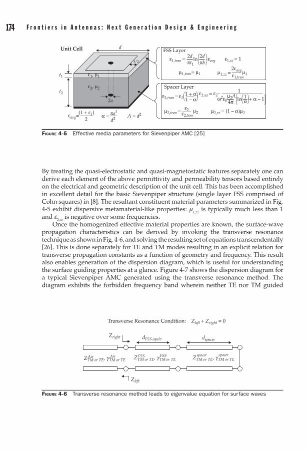
174 F r o n t i e r s i n A n t e n n a s : N e x t G e n e r a t i o n D e s i g n & E n g i n e e r i n g C h a p t e r 4 : A r t i f i c i a l M a g n e t i c C o n d u c t o r s / H i g h - I m p e d a n c e S u r f a c e s 175
By treating the quasi-electrostatic and quasi-magnetostatic features separately one can derive each element of the above permittivity and permeability tensors based entirely on the electrical and geometric description of the unit cell. This has been accomplished in excellent detail for the basic Sievenpiper structure (single layer FSS comprised of Cohn squares) in [8]. The resultant constituent material parameters summarized in Fig. 4-5 exhibit dispersive metamaterial-like properties: m1,zz is typically much less than 1 and e2,zz is negative over some frequencies.
Once the homogenized effective material properties are known, the surface-wave propagation characteristics can be derived by invoking the transverse resonance technique as shown in Fig. 4-6, and solving the resulting set of equations transcendentally [26]. This is done separately for TE and TM modes resulting in an explicit relation for transverse propagation constants as a function of geometry and frequency. This result also enables generation of the dispersion diagram, which is useful for understanding the surface guiding properties at a glance. Figure 4-7 shows the dispersion diagram for a typical Sievenpiper AMC generated using the transverse resonance method. The diagram exhibits the forbidden frequency band wherein neither TE nor TM guided
Figure 4-5 Effective media parameters for Sievenpiper AMC [25]
Unit Cell d
b/2
FSS Layer
Spacer Layer
2d
2εavg
2dε1,tran =
ε2,tran =
(1 + ε1)2
ε2.zz = ε2–
ε2,tran
ε2
ε1,tran
µ2A
µ1,tran= µ1
µ2,tran =
µ1
µ2 µ2,zz = (1 – α)µ2
α + α – 1ω2ε0 4π
πa2
µ1,zz =
εavg
εavg=
ε2, µ2
ε1, µ1
α =
ε2
ε1,zz = 1
1
πt1 πbln
1 + α1 – α ln 1
t1
t2
2a
A = d2
d2
Figure 4-6 Transverse resonance method leads to eigenvalue equation for surface waves
Transverse Resonance Condition: Zleft + Zright = 0
Zright
ZTM or TE, gTM or TE
dFSS.equiv dspacer
Zleft
Air Air ZTM or TE, gTM or TEFSS FSS ZTM or TE, gTM or TE
spacer spacer

174 F r o n t i e r s i n A n t e n n a s : N e x t G e n e r a t i o n D e s i g n & E n g i n e e r i n g C h a p t e r 4 : A r t i f i c i a l M a g n e t i c C o n d u c t o r s / H i g h - I m p e d a n c e S u r f a c e s 175
modes can propagate and shows that there are higher order TM modes, which can propagate at higher frequencies.
In examining the field distributions shown in Fig. 4-4, it is apparent that the TE mode has strong Hz and a large amount of the surface-wave energy is distributed within the FSS region, while the TM mode has strong Ez and a large amount of the surface-wave energy is distributed within the spacer region. Hence, it is somewhat intuitive that m1,zz would have a strong impact on TE surface waves and e2,zz would affect TM. It is interesting to note that the transverse resonance equations derived in [27] yield this exact relationship explicitly.
4.3.3 CEM Simulation of AMC StructuresFull-wave CEM solvers such as Ansoft HFSS or CST Microwave Studio can also be used to analyze the performance of an AMC. This can be done either by modeling a single unit cell with periodic boundary conditions to simulate an infinite array [27], [28] or, for sufficiently small geometries, by modeling the entire finite structure [29], [30]. This section provides a brief overview of the infinite array technique, which is usually the most practical approach.
Linked boundary conditions can be used to image a unit cell into an infinite array model, from which both surface reflection phase and surface-wave dispersion characteristics can be computed. The unit cell simulation setup for both of these cases is shown in Fig. 4-8.
Figure 4-7 Dispersion diagram for typical Sievenpiper AMC
TMTMTMTE
50
45
40
35
30
20
25
15
10
5
00 200 400 600 800 1000 1200
Freq
uenc
y (G
Hz)
βx (rad/m)
Bandgap

176 F r o n t i e r s i n A n t e n n a s : N e x t G e n e r a t i o n D e s i g n & E n g i n e e r i n g C h a p t e r 4 : A r t i f i c i a l M a g n e t i c C o n d u c t o r s / H i g h - I m p e d a n c e S u r f a c e s 177
In the model, a perfectly matched layer (PML) is placed atop an airbox that is over the AMC unit cell. This is an effective method to simulate an infinite half-space over the AMC, provided that the PML is sufficiently far enough above the surface of the AMC to allow the fields to achieve steady state (six times the AMC thickness according to [27]). Master-slave boundaries are then defined along the side walls. This establishes a user-defined phase difference (y ) between the electric fields at each point on the slave boundary (ES) and its corresponding point on the master boundary (EM) as shown in (4-4).
ES = EMejy (4-4)
In the reflection phase analysis, an incident plane wave is used to excite the structure and the fields are evaluated over a plane just below the PML. In the case of HFSS, Optimetrics can be used to drive a simulation that uses the Field Calculator to post-process the field data to yield reflection phase versus frequency.
In the dispersion analysis, Optimetrics can be used to sweep the master-slave phase relationship and the eigenmode solver is invoked to calculate the permitted eigen-frequencies of the structure for each phase difference (y ). In this manner, the relationship between frequency and the associated transverse propagation constant is established, providing a discretized version of the dispersion diagram. By varying the phase relation between master-slave boundaries in X and Y, the analysis can be carried out over the entire irreducible Brillouin zone, the nonredundant set of propagation directions whose geometry varies depending on the symmetry of the unit cell [6]. However, as stated previously, for AMCs with electrically small unit cells it is usually sufficient to calculate the dispersion along a single transverse direction as the performance is only weakly dependent on the direction of transverse propagation. Figure 4-9 shows the dispersion diagram generated using this method in HFSS overlaid with that generated using the transverse resonance method for a typical Sievenpiper AMC. The figure shows reasonably good agreement between the two techniques.
Figure 4-8 Simulation space setup for the AMC (a) reflectivity and (b) dispersion analyses
Perfectly Matched Layer(PML)
ObservationPlane
Air
Slave Y
Slav
e X
Mas
ter X
Sourcek
AMC
Ground
(a)
Y
X
E0
Perfectly Matched Layer(PML)
Air
Slave Y
Master Y
Slav
e X
Mas
ter X
AMC
Ground
(b)
Y
X
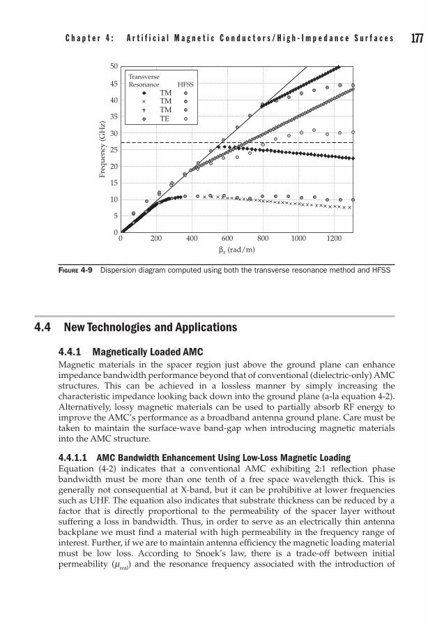
176 F r o n t i e r s i n A n t e n n a s : N e x t G e n e r a t i o n D e s i g n & E n g i n e e r i n g C h a p t e r 4 : A r t i f i c i a l M a g n e t i c C o n d u c t o r s / H i g h - I m p e d a n c e S u r f a c e s 177
4.4 New Technologies and Applications
4.4.1 Magnetically Loaded AMCMagnetic materials in the spacer region just above the ground plane can enhance impedance bandwidth performance beyond that of conventional (dielectric-only) AMC structures. This can be achieved in a lossless manner by simply increasing the characteristic impedance looking back down into the ground plane (a-la equation 4-2). Alternatively, lossy magnetic materials can be used to partially absorb RF energy to improve the AMC’s performance as a broadband antenna ground plane. Care must be taken to maintain the surface-wave band-gap when introducing magnetic materials into the AMC structure.
4.4.1.1 AMC Bandwidth Enhancement Using Low-Loss Magnetic LoadingEquation (4-2) indicates that a conventional AMC exhibiting 2:1 reflection phase bandwidth must be more than one tenth of a free space wavelength thick. This is generally not consequential at X-band, but it can be prohibitive at lower frequencies such as UHF. The equation also indicates that substrate thickness can be reduced by a factor that is directly proportional to the permeability of the spacer layer without suffering a loss in bandwidth. Thus, in order to serve as an electrically thin antenna backplane we must find a material with high permeability in the frequency range of interest. Further, if we are to maintain antenna efficiency the magnetic loading material must be low loss. According to Snoek’s law, there is a trade-off between initial permeability (mreal) and the resonance frequency associated with the introduction of
Figure 4-9 Dispersion diagram computed using both the transverse resonance method and HFSS
50
45
40
35
30
20
25
15
10
5
00 200 400 600 800 1000 1200
Freq
uenc
y (G
Hz)
βx (rad/m)
TMTMTMTE
TransverseResonance HFSS
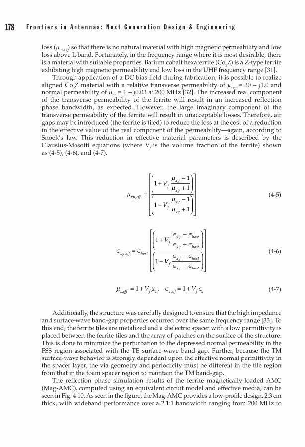
178 F r o n t i e r s i n A n t e n n a s : N e x t G e n e r a t i o n D e s i g n & E n g i n e e r i n g C h a p t e r 4 : A r t i f i c i a l M a g n e t i c C o n d u c t o r s / H i g h - I m p e d a n c e S u r f a c e s 179
loss (mimag) so that there is no natural material with high magnetic permeability and low loss above L-band. Fortunately, in the frequency range where it is most desirable, there is a material with suitable properties. Barium cobalt hexaferrite (Co2Z) is a Z-type ferrite exhibiting high magnetic permeability and low loss in the UHF frequency range [31].
Through application of a DC bias field during fabrication, it is possible to realize aligned Co2Z material with a relative transverse permeability of mr,xy ≅ 30 - j1.0 and normal permeability of mr,z ≅ 1 - j0.03 at 200 MHz [32]. The increased real component of the transverse permeability of the ferrite will result in an increased reflection phase bandwidth, as expected. However, the large imaginary component of the transverse permeability of the ferrite will result in unacceptable losses. Therefore, air gaps may be introduced (the ferrite is tiled) to reduce the loss at the cost of a reduction in the effective value of the real component of the permeability—again, according to Snoek’s law. This reduction in effective material parameters is described by the Clausius-Mosotti equations (where Vf is the volume fraction of the ferrite) shown as (4-5), (4-6), and (4-7).
µ
µµ
µµ
xy eff
fxy
xy
fxy
xy
V
V, =
+-+
--+
11
1
11
1
(4-5)
∈ ∈
∈ ∈∈ ∈
xy eff host
fxy host
xy host
V
, =
+-+
-
1
1 VVfxy host
xy host
∈ ∈∈ ∈
-+
(4-6)
µ µz eff f z z eff f zV V, ,,= + = +1 1∈ ∈
(4-7)
Additionally, the structure was carefully designed to ensure that the high impedance and surface-wave band-gap properties occurred over the same frequency range [33]. To this end, the ferrite tiles are metalized and a dielectric spacer with a low permittivity is placed between the ferrite tiles and the array of patches on the surface of the structure. This is done to minimize the perturbation to the depressed normal permeability in the FSS region associated with the TE surface-wave band-gap. Further, because the TM surface-wave behavior is strongly dependent upon the effective normal permittivity in the spacer layer, the via geometry and periodicity must be different in the tile region from that in the foam spacer region to maintain the TM band-gap.
The reflection phase simulation results of the ferrite magnetically-loaded AMC (Mag-AMC), computed using an equivalent circuit model and effective media, can be seen in Fig. 4-10. As seen in the figure, the Mag-AMC provides a low-profile design, 2.3 cm thick, with wideband performance over a 2.1:1 bandwidth ranging from 200 MHz to

178 F r o n t i e r s i n A n t e n n a s : N e x t G e n e r a t i o n D e s i g n & E n g i n e e r i n g C h a p t e r 4 : A r t i f i c i a l M a g n e t i c C o n d u c t o r s / H i g h - I m p e d a n c e S u r f a c e s 179
419 MHz. A conventional Sievenpiper AMC providing similar wideband performance would require a thickness of nearly 5 times that of the Mag-AMC.
A prototype of the Mag-AMC was fabricated and experimentally tested. The Mag-AMC, shown in Fig. 4-11, was fabricated by placing metalized ferrite tiles in a guiding dielectric lattice over a metal ground plane. Metal vias were used to connect the metalized surface of each ferrite tile to the metal ground plane. Rohacell foam with a lattice of metal patches was placed over the lattice of ferrite tiles. Metal vias were used to connect the metal patches on the surface of the Rohacell foam to the metal ground plane.
The reflection phase of the Mag-AMC was measured over a frequency range of 200 MHz to 500 MHz. Simulated and measured results for the Mag-AMC are shown in Figs. 4-10 and 4-12. The reflection phase comparison shows good agreement between the measured and simulated data. The measured reflection phase bandwidth covers 236 MHz to 402 MHz, a 1.7:1 bandwidth, while the simulated reflection phase bandwidth covers 200 MHz to 419 MHz, a 2.1:1 bandwidth. The discrepancies between the measured and simulated results can be attributed to edge diffraction that results from the limited electrical size of the Mag-AMC.
Figure 4-10 Mag-AMC and reflection phase of the structure
Simulated Mag-AMC
Simulated Foam AMCMeasured Foam AMC
Measured Mag-AMC
120
Reflection Phase Comparison forMag-AMC and Foam AMC
90
60
30
0
–30
–60
–90
–120
Ref
lect
ion
Phas
e, [d
eg]
200 250 300 350
Frequency, [MHz]
400 450 500
Figure 4-11 Prototype of the fabricated Mag-AMC

180 F r o n t i e r s i n A n t e n n a s : N e x t G e n e r a t i o n D e s i g n & E n g i n e e r i n g C h a p t e r 4 : A r t i f i c i a l M a g n e t i c C o n d u c t o r s / H i g h - I m p e d a n c e S u r f a c e s 181
4.4.1.2 Bandwidth Enhancement Using Lossy Magnetically Loaded AMCsRF absorbers are sometimes used over conductive ground planes to back antennas to achieve good broadband VSWR performance within a low-profile structure. Another antenna ground plane option used to achieve similar results without incurring the loss introduced by the absorber is an AMC. In this section a hybrid design approach is pursued to engineer an antenna ground plane that, when placed closely behind an antenna, will not degrade the VSWR performance over an ultrawide bandwidth. The hybrid structure consists of a Sievenpiper AMC with a thin layer of ferrite absorber placed along the ground plane [34]. In the lower frequency band, the hybrid structure provides a surface impedance that takes advantage of the lossy characteristics of the ferrite absorber and provides significant absorption. In the higher frequency band, the hybrid structure provides the high surface impedance characteristics of an AMC and provides the reflected radiation with a desirable phase. While the structure is still lossy in the AMC region of operation, there is enough energy reflected from the structure to provide a noticeable increase in antenna gain.
Simulations were performed to determine the performance of the hybrid structure concept. The first simulations performed determined the reflection magnitude (reflectivity) and the reflection phase of the structure. The reflectivity and reflection phase simulation results of the hybrid structure design are shown in Fig. 4-13. The absorber region of operation is defined where less than –14 dB of reflectivity is achieved. The AMC region of operation is defined where the phase of the reflected radiation is between ±90° regardless of the reflectivity. The operational bandwidth of the hybrid structure is defined where either one or both of these criteria are met. As Fig. 4-13 depicts, the hybrid structure provides a low-profile design, 2.5 cm thick, with ultra-wideband operation over a 40.5:1 bandwidth ranging from 120 MHz to 4.86 GHz. The absorber region provides operation over a 27.8:1 bandwidth ranging from 120 MHz to 3.33 GHz while the AMC region provides operation over a 1.8:1 bandwidth ranging from 2.65 GHz to 4.86 GHz.
Figure 4-12 Mag-AMC versus conventional Sievenpiper AMC
xx
2.6
2.4
2.2
2.0
1.8
1.6
1.4
1.2
1.0
f_hi
gh/
f_lo
w
0.00 0.02 0.04 0.06 0.08Normalized Height (h/λ0)
0.10 0.12 0.14 0.16 0.18
h
Using Magnetic Tiles
Sievenpiper AMC
“Thick“ FoamCore AMC
x
TheoryFullwave Sol’nMeasurement

180 F r o n t i e r s i n A n t e n n a s : N e x t G e n e r a t i o n D e s i g n & E n g i n e e r i n g C h a p t e r 4 : A r t i f i c i a l M a g n e t i c C o n d u c t o r s / H i g h - I m p e d a n c e S u r f a c e s 181
As shown through the reflectivity and reflection phase results, the hybrid structure offers enticing characteristics as a low-profile, ultra-wideband ground plane. However, to fully understand how the structure will perform as a ground plane, the implementation of the hybrid structure with a bidirectional radiating antenna (long slot array antenna [35]–[37]) was simulated. The simulated implementation can be seen in Fig. 4-14.
The radiation patterns of a single unit cell of the long slot array antenna and hybrid structure combination were simulated first. A single unit cell of the combination consisted of 4 × 4 elements of the long slot array antenna above a single element of the hybrid structure. Periodic boundary conditions were used to simulate an infinite array of this combination and the radiation patterns were calculated for a single unit cell. The directive gain versus frequency for the long slot array antenna above the hybrid structure was compared to the theoretical maximum directive gain for an unbacked
long slot array GA=
22
πλ
. Figure 4-15 shows there is an increase in the directive gain of
the long slot array antenna above the hybrid structure operating in the AMC region of operation compared to the theoretical maximum directive gain of the long slot array antenna in free space. Fig. 4-15 also shows that, in the absorber region of operation, the directive gain of the implementation is slightly less than the theoretical maximum directive gain. This is believed to be due to the proximity of the antenna to the hybrid structure, which becomes electrically small in the absorber region of operation. The return loss,
Figure 4-14 Simulated implementation of the long slot array antenna above the hybrid structure
Long Slot Array Antenna
Hybrid Ground Plane
18.50 mm
3.70 mm
2.50
mm
6.70
mm
25.0
0 m
m
3.70
mm
18.5
0 m
m
Figure 4-13 Unit cell of the hybrid structure and reflectivity and reflection phase of the structure
0 dB 180°
90°
0°
–90°
–180°
–4 dB
–8 dB
–12 dB
–14 dB
–16 dB
0.100 GHz 1.325 GHz 2.550 GHz
Frequency
3.775 GHz 5.000 GHz
Phas
e
Ref
lect
ivit
y
Hybrid Ground Plane Reflection Analysis
Sievenpiper AMC
Ferrite Tile Absorber
15.00 mm
19.75 mm
37.0
0 m
m
25.0
0 m
m6.
70 m
m
ReflectivityPhase

182 F r o n t i e r s i n A n t e n n a s : N e x t G e n e r a t i o n D e s i g n & E n g i n e e r i n g C h a p t e r 4 : A r t i f i c i a l M a g n e t i c C o n d u c t o r s / H i g h - I m p e d a n c e S u r f a c e s 183
shown in Fig. 4-15, for the feed system of the long slot array antenna above the hybrid structure was also simulated. The return loss results verify that the implementation of an ultra-wideband bidirectional radiating antenna and the hybrid structure provide acceptable operational performance over a 40.5:1 bandwidth ranging from 120 MHz to 4.86 GHz.
To validate the simulation results, a prototype of the hybrid structure was fabricated and two characteristics of the structure were measured. The measured characteristics include the reflection properties, reflectivity, and reflection phase, as well as the surface-wave suppression properties. ETS-Lindgren’s FT-2000 ferrite absorber, square stainless steel washers, stainless steel machine screws, and a sheet of aluminum were used to fabricate the prototype hybrid structure as shown in Fig. 4-16.
Figure 4-15 Directive gain and return loss of the long slot array antenna above the hybrid structure
10 dBi 0 dB
–5 dB
–10 dB
–15 dB
–20 dB
0 dBi
–10 dBi
–20 dBi
–30 dBi
Dir
ecti
ve G
ain
Ret
urn
Los
s
0.120 GHz 1.305 GHz 2.490 GHzFrequency
3.675 GHz 4.860 GHz
Hybrid Ground Plane/Long Slot Array Analysis
Theoretical Maximum Directive Gain for UnbackedLong Slot Array (calculated for single unit cell)Simulated Directive Gain of Hybrid Ground Plane and LongSlot Array Implementation (calculated for single unit cell)Simulated Return Loss of Hybrid Ground Planeand Long Slot Array Implementation
Figure 4-16 Fabricated hybrid structure prototype
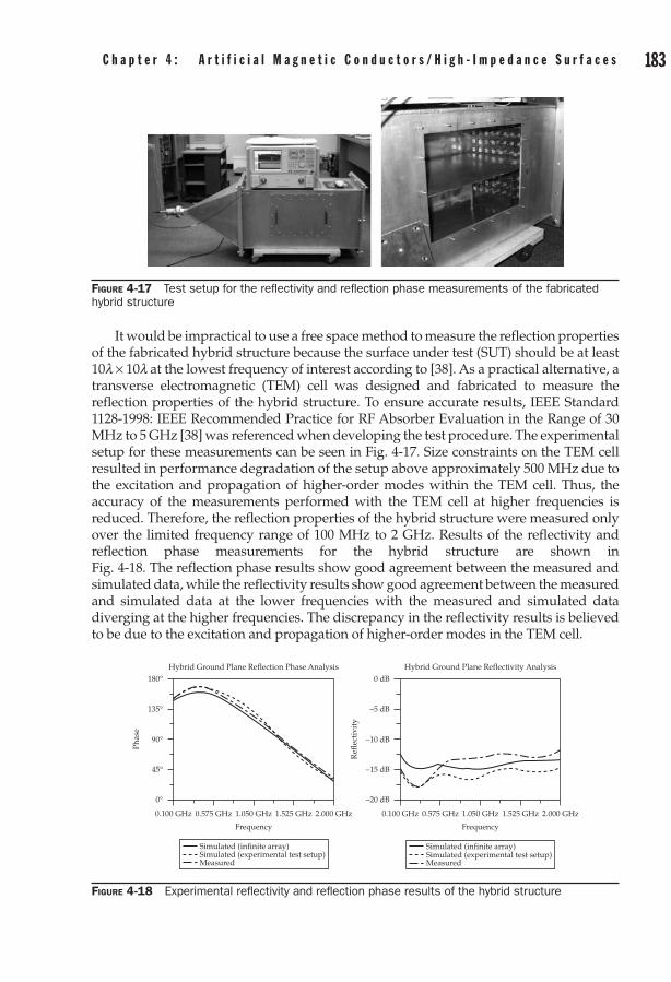
182 F r o n t i e r s i n A n t e n n a s : N e x t G e n e r a t i o n D e s i g n & E n g i n e e r i n g C h a p t e r 4 : A r t i f i c i a l M a g n e t i c C o n d u c t o r s / H i g h - I m p e d a n c e S u r f a c e s 183
It would be impractical to use a free space method to measure the reflection properties of the fabricated hybrid structure because the surface under test (SUT) should be at least 10l × 10l at the lowest frequency of interest according to [38]. As a practical alternative, a transverse electromagnetic (TEM) cell was designed and fabricated to measure the reflection properties of the hybrid structure. To ensure accurate results, IEEE Standard 1128-1998: IEEE Recommended Practice for RF Absorber Evaluation in the Range of 30 MHz to 5 GHz [38] was referenced when developing the test procedure. The experimental setup for these measurements can be seen in Fig. 4-17. Size constraints on the TEM cell resulted in performance degradation of the setup above approximately 500 MHz due to the excitation and propagation of higher-order modes within the TEM cell. Thus, the accuracy of the measurements performed with the TEM cell at higher frequencies is reduced. Therefore, the reflection properties of the hybrid structure were measured only over the limited frequency range of 100 MHz to 2 GHz. Results of the reflectivity and reflection phase measurements for the hybrid structure are shown in Fig. 4-18. The reflection phase results show good agreement between the measured and simulated data, while the reflectivity results show good agreement between the measured and simulated data at the lower frequencies with the measured and simulated data diverging at the higher frequencies. The discrepancy in the reflectivity results is believed to be due to the excitation and propagation of higher-order modes in the TEM cell.
Figure 4-17 Test setup for the reflectivity and reflection phase measurements of the fabricated hybrid structure
Figure 4-18 Experimental reflectivity and reflection phase results of the hybrid structure
180°
135°
90°
45°
0°
Phas
e
0.100 GHz 0.575 GHz 1.050 GHz
Frequency
1.525 GHz 2.000 GHz
Hybrid Ground Plane Reflection Phase Analysis0 dB
–5 dB
–10 dB
–15 dB
–20 dB
Ref
lect
ivit
y
0.100 GHz 0.575 GHz 1.050 GHz
Frequency
1.525 GHz 2.000 GHz
Hybrid Ground Plane Reflectivity Analysis
Simulated (infinite array)Simulated (experimental test setup)Measured
Simulated (infinite array)Simulated (experimental test setup)Measured

184 F r o n t i e r s i n A n t e n n a s : N e x t G e n e r a t i o n D e s i g n & E n g i n e e r i n g C h a p t e r 4 : A r t i f i c i a l M a g n e t i c C o n d u c t o r s / H i g h - I m p e d a n c e S u r f a c e s 185
Surface-wave transmission or suppression can be measured by observing the amount of energy transmitted between two linearly polarized antennas placed at either edge of the SUT. To ensure accurate experimental surface-wave suppression results, the methods described in [1] and [39] were referenced when developing the test procedure. The experimental setup for these measurements can be seen in Fig. 4-19. The experimental setup entailed placing the SUT on a piece of polyethylene foam absorber with another piece of polyethylene foam absorber mounted a small distance above the SUT. The purpose of the polyethylene foam absorber is to reduce the free space coupling between the measurement antennas. The surface-wave suppression properties of the hybrid structure were measured over the frequency range of 800 MHz to 4 GHz. Measurement results of this analysis are shown in Fig. 4-20. The TM surface-wave suppression provided by the hybrid structure is shown to be at least 20 dB more than that of the electric conductor with the suppression exceeding 60 dB in the AMC region of operation. Between 1.2 GHz and 1.3 GHz there is an increase in TM surface-wave suppression exceeding 25 dB, which indicates the edge of the TM surface-wave suppression band and corresponds well with the 1.39 GHz +90° reflection phase seen in the measured
Figure 4-19 Test setup for the surface-wave suppression measurements of the fabricated hybrid structure
Figure 4-20 Experimental surface-wave suppression results of the hybrid structure
0 dB
–25 dB
–50 dB
–75 dB
–100 dB
0.8 GHz 1.6 GHz 2.4 GHz
Frequency
Tran
smis
sion
3.2 GHz 4.0 GHz
TM Mode Surface-Wave Transmission
Electric Conductor (TM)Ferrite Absorber (TM)Hybrid Structure (TM)
0 dB
–25 dB
–50 dB
–75 dB
–100 dB
0.8 GHz 1.6 GHz 2.4 GHz
Frequency
Tran
smis
sion
3.2 GHz 4.0 GHz
TE Mode Surface-Wave Transmission
Electric Conductor (TE)Ferrite Absorber (TE)Hybrid Structure (TE)
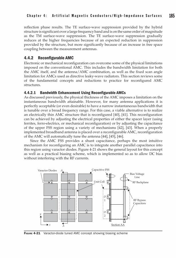
184 F r o n t i e r s i n A n t e n n a s : N e x t G e n e r a t i o n D e s i g n & E n g i n e e r i n g C h a p t e r 4 : A r t i f i c i a l M a g n e t i c C o n d u c t o r s / H i g h - I m p e d a n c e S u r f a c e s 185
reflection phase results. The TE surface-wave suppression provided by the hybrid structure is significant over a large frequency band and is on the same order of magnitude as the TM surface-wave suppression. The TE surface-wave suppression gradually reduces at the higher frequencies because of an expected reduction in suppression provided by the structure, but more significantly because of an increase in free space coupling between the measurement antennas.
4.4.2 Reconfigurable AMCElectronic or mechanical reconfiguration can overcome some of the physical limitations imposed on the conventional AMC. This includes the bandwidth limitation for both the AMC itself, and the antenna/AMC combination, as well as the fixed scan angle limitation for AMCs used as directive leaky-wave radiators. This section reviews some of the fundamental concepts and reductions to practice for reconfigured AMC structures.
4.4.2.1 Bandwidth Enhancement Using Reconfigurable AMCsAs discussed previously, the physical thickness of the AMC imposes a limitation on the instantaneous bandwidth attainable. However, for many antenna applications it is perfectly acceptable (or even desirable) to have a narrow instantaneous bandwidth that is tunable over a broad frequency range. For this case, a viable alternative is to realize an electrically thin AMC structure that is reconfigured [40], [41]. This reconfiguration can be achieved by adjusting the electrical properties of either the spacer layer (using ferrites, ferro-electrics, or mechanical reconfiguration) or by adjusting the capacitance of the upper FSS region using a variety of mechanisms [42], [43]. When a properly implemented broadband antenna is placed over a reconfigurable AMC, reconfiguration of the AMC will automatically tune the antenna [44], [45], [46].
Since the AMC FSS provides a shunt capacitance, perhaps the most intuitive mechanism for reconfiguring an AMC is to integrate another parallel capacitance into this region using varactor diodes. Figure 4-21 shows the general layout for this concept as well as a practical biasing scheme, which is implemented so as to allow DC bias without interfering with the RF currents.
Figure 4-21 Varactor-diode tuned AMC concept showing biasing scheme
Varactor Diodes A Capacitive FSS
y
x A
Unit Cell
D
D
Section AA
1
2
Bias VoltageLine
RF Backplane
RF BypassCapacitors

186 F r o n t i e r s i n A n t e n n a s : N e x t G e n e r a t i o n D e s i g n & E n g i n e e r i n g C h a p t e r 4 : A r t i f i c i a l M a g n e t i c C o n d u c t o r s / H i g h - I m p e d a n c e S u r f a c e s 187
In the embodiment shown here, biasing is accomplished by using the vias, indigenous to the AMC, to route DC bias currents from stripline control lines buried inside the RF backplane. RF bypass capacitors are used to decouple RF current at the base of the biasing vias. In practice, the varactors can be installed in a “thinned” pattern (i.e., one varactor for every N unit cells) so as to reduce the number of varactors per unit area and hence the cost, weight, and complexity. To ensure an equal voltage drop across each diode in the series string that is found between the DC bias vias and the ground vias in a thinned configuration, a ballast resistor of large value can be placed in parallel with each diode. Figure 4-22 shows the measured reflection phase versus frequency for an implementation of this type of reconfigurable AMC, parameterized by bias voltage from [39].
The figure shows that the high-impedance band of the AMC is tunable over more than a 3:1 bandwidth. Surface-wave measurements similar to those described in Section 4.4.1 were performed and show that the surface-wave band-gap for this structure also tunes with bias voltage. Thus, the two properties required for operation as a good antenna backplane were demonstrated to tune in concert. Antenna performance was verified by placing a broadband spiral over the AMC (see Fig. 4-23) and measuring input impedance, boresight gain, and radiation patterns. The results, contained in [39], show that the viable operational band of the antenna is tuned by the AMC backplane, and that over this tunable band, the antenna gain is 3 dB greater than for the case of the same spiral antenna with a conventional absorber backing.
The above example describes an analog mechanism for reconfiguring the AMC FSS. That is, the operational band can be continuously swept over its range, limited only by the resolution of the applied bias voltage circuitry. This has also been demonstrated in [47].
Figure 4-22 Measured reflection phase of the varactor-tuned AMC parameterized by bias voltage
0 V5 V10 V15 V20 V25 V30 V35 V40 V45 V50 V
Reflection Phase Measurements: Varactor-Tuned AMC
150
100
50
0
–50
–100
–150
Ref
lect
ion
Phas
e (d
eg)
400 600 800 1000 1200 1400 1600 1800 2000 2200 2400Frequency (MHz)

186 F r o n t i e r s i n A n t e n n a s : N e x t G e n e r a t i o n D e s i g n & E n g i n e e r i n g C h a p t e r 4 : A r t i f i c i a l M a g n e t i c C o n d u c t o r s / H i g h - I m p e d a n c e S u r f a c e s 187
The downside of this method is that, for applications requiring higher transmit powers, the imposed RF signal may modulate the diode bias voltage, causing intermodulation distortion in the transmitted waveform. In order to mitigate this effect, one may employ highly linear variable capacitors, each of which contain arrays of series capacitors. An alternative approach is to use on/off type devices such as PIN diodes or MEMs switches to discretely tune the FSS region capacitance.
An example of a discretely tuned AMC structure using on/off mechanisms is shown in Fig. 4-24, and is described in [48]. In this structure, the AMC is reconfigured by switching in and out varying amounts of capacitance, in the form of physical overlap of a two-layer FSS, by using PIN diodes or MEMs switches. This approach may have advantages in power handling over the varactor case. Also, because the two-layer FSS geometry can obtain very large capacitances per unit area, this approach may also yield a significantly greater tuning range versus the varactor approach. This type of tuning mechanism has also been successfully demonstrated in [49].
Figure 4-23 Printed spiral antenna over reconfigurable AMC
Figure 4-24 Unit cell of AMC with switched capacitance showing bias configuration
FSS Unit Cell:
AMC Cross-section:
CapacitiveFSS
AccessVias
RF Backplane RF BypassCapacitors
VC1
VC2

188 F r o n t i e r s i n A n t e n n a s : N e x t G e n e r a t i o n D e s i g n & E n g i n e e r i n g C h a p t e r 4 : A r t i f i c i a l M a g n e t i c C o n d u c t o r s / H i g h - I m p e d a n c e S u r f a c e s 189
The tuning approaches discussed thus far have described mechanisms for tuning the capacitive top layer or FSS region of the AMC. However, as described in Section 4.3, the AMC can be viewed as an L-C resonator, so we may also consider tuning the inductance associated with the bottom or spacer layer. Since the inductance in this region can be viewed as arising from a short length of transmission line, we can consider tuning mechanisms associated with transmission line parameters. This means changing the propagation constant along the transmission line or changing the overall length. The former mechanism can be accomplished by using tunable materials such as biased ferrites or ferroelectrics [50]. The latter can be accomplished by physically adjusting the height of the structure. This is described in [51] and is shown in Fig. 4-25. In the figure, the vias are realized using spring contact probes, which maintain electrical contact between the AMC patches and the ground plane over some range of spacer height. Stepper motors (or other mechanisms) connected to threaded shafts around the periphery of the structure can be used to adjust the height of the rigid FSS layer over the RF backplane, thus tuning the AMC resonant frequency. The benefits of this type of tuning include minimal impact to power-handling and linearity. The downsides include an increase in mechanical complexity and tuning speed that is orders of magnitude slower than what is obtainable using electronic methods.
4.4.2.2 Beamsteering Capabilities Using Electronically Reconfigurable AMCsInitial AMC antenna constructs, circa 2000, were focused primarily on achieving efficiency and bandwidth in an electrically thin package with little attention devoted to directivity in the radiated pattern. As the technology matured and the leaky-wave nature of TE surface-waves just below cutoff were understood, the concept of exciting the AMC surface itself to produce a directive beam was developed [25], [52]. In this work, varactors were used to modify the dispersion diagram (see Fig. 4-26) such that the radiation angle of the leaked energy adjusted itself to match the transverse phase velocity of the tangential component of the bound mode. In this way a direct relation between radiation angle and applied DC bias was established, and one-dimensional steering of a fan-beam was accomplished.
More recent developments in this area combine the ideas of surface impedance modulation and microwave holography to achieve more-robust control of the far-field radiation pattern [53]. In this work a waveguide is used to excite the surface of an AMC
Figure 4-25 Schematic of mechanically tunable AMC where resonance is adjusted by stepping FSS height
Air Spacer layer toAllow for height adjustment
FSS Finely Threaded shaft
StepperMotor
RF Ground Plane
Dielectric Substrate
Spring Contact Probes
Probe Receptacle

188 F r o n t i e r s i n A n t e n n a s : N e x t G e n e r a t i o n D e s i g n & E n g i n e e r i n g C h a p t e r 4 : A r t i f i c i a l M a g n e t i c C o n d u c t o r s / H i g h - I m p e d a n c e S u r f a c e s 189
whose impedance is modulated with varactor diodes as shown in Fig. 4-27. The surface impedance modulation is chosen in accordance with holographic principles which, in this case means the interference pattern between the expected bound surface wave and the desired outgoing plane wave. Experimental results (Fig. 4-28) show that two-dimensional scan of a pencil-beam is attainable.
In the above cited work, the source antenna is located coplanar to the surface of the AMC resulting in a low-profile antenna/AMC structure. Another reconfigurable configuration of interest is to have the source antenna above the plane of the AMC. In this case, the AMC can be considered a special case of a reflect array [54], [55].
Figure 4-26 Dispersion diagram showing tuning of leaky-wave region
Radiation ConeBound
TE Modes
BoundTM Modes
LeakyTE Modes
Bri
lloui
n Z
one
Gap
k2 k1kII
ω
ω = ck
ωAω2ω1
Figure 4-27 Photograph of tunable AMC hardware and example holographic impedance map for θ = 45°, φ = 30° scan
10 15 20 25 30X-axis unit cell index
35 40 45 50 55 60 65 70 75 805
5
10
15
20
25
30
35
40
Y-ax
is U
nit C
ell I
ndex
330
268
205
142
80
Surf
ace
Rea
ctan
ce S
cale
(a) (b)
z
xy
160 mm
320 m
m

190 F r o n t i e r s i n A n t e n n a s : N e x t G e n e r a t i o n D e s i g n & E n g i n e e r i n g C h a p t e r 4 : A r t i f i c i a l M a g n e t i c C o n d u c t o r s / H i g h - I m p e d a n c e S u r f a c e s 191
4.4.3 Novel AMC ConstructsAs previously described, the Sievenpiper AMC [1] is an attractive technology to implement as a ground plane for low-profile, unidirectional radiating antenna systems. However, their attractive magnetic conductor characteristics are band limited. Additionally, these AMCs are limited to operation at relatively higher frequency bands because of the high capacitive and/or inductive characteristics needed to operate in lower frequency bands. A few of the developing alternative AMC technologies being employed to reduce these inherent limitations have been described in detail in this chapter. There are other exciting alternative AMC technologies being explored. However, due to space considerations, all of these approaches cannot be described in detail. Thus, for completeness, a few of these novel AMC constructs will be briefly discussed. These novel AMC constructs include aperiodic AMCs [56], genetic algorithm generated AMCs [57], multilayered AMCs [20], [58], and negative impedance AMCs [59].
4.4.3.1 Aperiodic AMCsAperiodically ordered mushroom-type AMCs that implement various surface patch geometries can be implemented to achieve larger band-gaps and multiple frequencies of operation. The study presented in [56] analyzes the performance of three aperiodically ordered AMCs with surface patch geometries consisting of squares, rhombuses, and triangles as seen in Fig. 4-29. It should be noted that, because of the aperiodicity of the structures analyzed, the typical approach to simulating these structures with unit cells and periodic boundary conditions was not used. Instead, finite size AMCs were implemented at a suitable size for simulation purposes while maintaining the symmetry centers.
The return loss and radiation patterns of a dipole antenna above each of the structures were simulated. The return loss results of the dipole above each of the four AMCs analyzed are shown in Fig. 4-30. It can be seen that the aperiodically tiled structures offer wider impedance matching bandwidths compared to periodically tiled structures. The radiation patterns of the dipole above each of the four structures
Figure 4-28 Measured radiation pattern in the XZ-plane at 5.5 GHz for noted scan angle settings
Scan Angle Settingt = 60 deg., p = 0 deg.t = 45 deg., p = 0 deg.t = 30 deg., p = 0 deg.t = 15 deg., p = 0 deg.
t = 15 deg., p = 180 deg.t = 30 deg., p = 180 deg.t = 45 deg., p = 180 deg.t = 60 deg., p = 180 deg.
t = 0 deg.
10 dBi
5 dBi
Feed
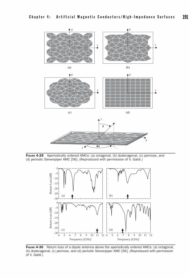
190 F r o n t i e r s i n A n t e n n a s : N e x t G e n e r a t i o n D e s i g n & E n g i n e e r i n g C h a p t e r 4 : A r t i f i c i a l M a g n e t i c C o n d u c t o r s / H i g h - I m p e d a n c e S u r f a c e s 191
Figure 4-30 Return loss of a dipole antenna above the aperiodically ordered AMCs: (a) octagonal, (b) dodecagonal, (c) penrose, and (d) periodic Sievenpiper AMC [56]. (Reproduced with permission of V. Galdi.)
–30
–25
–20
–15
–10
–5
0
Ret
urn
Loss
[dB]
4 5 6 7 8 9 10 11 12–30
–25
–20
–15
–10
–5
0
Ret
urn
Loss
[dB]
4 5 6 7 8 9 10 11 12Frequency [GHz] Frequency [GHz]
(a) (b)
(c) (d)
Figure 4-29 Aperiodically ordered AMCs: (a) octagonal, (b) dodecagonal, (c) penrose, and (d) periodic Sievenpiper AMC [56]. (Reproduced with permission of V. Galdi.)
... .
..
.. .
.. . .
.. . . . . .
. .. . . . .
..
..
. . ...
... .
..
.....
.
. ....
..
. .. .
..
..
.
.
..
..
.
...
..
.
.
....
...
.
.
...
... .
. ..
....
..
...
...
. ... . .
.. .
.. . .
..
.. . .
.. .. .
...
..
....
...
...
. ..
..
. ... .
......
....
. ..
. ...
.. .
. ..
. .
.
.
.
.
.
.
.
.
.
.
.
.
.
.
.
.
.
.
.
.
.
.
.
.
.
.
.
.
.
.
.
.
.
.
.
.
.
.
.
.
.
.
.
.
.
.
.
.
.
.
.
.
.
.
.
.
.
.
.
.
.
.
.
.
.
.
.
.
.
.
.
.
.
.
.
.
.
.
.
.
.
.
...
..
....
.
. . ..
...
..
.....
. . ....
. ..... . . ... ... .. . . .. . . . . . . .....
. .... . ..
.... . .
. . . ......
. . .. . ..
....
. ......
..
..
...
... .
.. . .
.
..
.
y
x
y
x
y
x
y
x
z
θ
y
x φ
(a)
(c) (d)
(e)
(b)

192 F r o n t i e r s i n A n t e n n a s : N e x t G e n e r a t i o n D e s i g n & E n g i n e e r i n g C h a p t e r 4 : A r t i f i c i a l M a g n e t i c C o n d u c t o r s / H i g h - I m p e d a n c e S u r f a c e s 193
analyzed can be seen in Fig. 4-31. The frequencies analyzed for the radiation pattern study, indicated by the arrows in Fig. 4-30, were chosen by determining the frequency that offered a reasonable trade-off between high broadside directivity and low return loss. The dipole above each of the aperiodically tiled structures showed higher broadside directivity compared to the dipole antenna above the periodically tiled structure. The radiation pattern of the dipole antenna above the periodically tiled structure was not simulated at the optimal frequency according to return loss because the radiation pattern exhibited mainlobe splitting at the frequency where the match was optimal. The surface-wave suppression properties of the finite size AMCs were analyzed by simulating two horizontally polarized dipoles on either side of the structures (TE mode) and two vertically polarized monopoles on either side of the structures (TM mode). The aperiodically tiled structures exhibited several TE surface-wave band-gaps indicating multiband operation. Conversely, the periodically tiled structure exhibited one TE surface-wave band-gap. The aperiodically tiled and periodically tiled structures exhibited several TM surface-wave band-gaps. With the proposed approaches in [56], it is feasible that broadband operation and/or multiband operation can be achieved. However, more study is necessary to completely characterize these aperiodically tiled structures.
Figure 4-31 Radiation patterns of a dipole antenna above the aperiodically ordered AMCs: (a) octagonal, (b) dodecagonal, (c) penrose, and (d) periodic Sievenpiper AMC [56]. (Reproduced with permission of V. Galdi.)
030
60
90
120
150180
210
240
270
300
330
–30–20–10
0
–40–30–20–10
0
(a)
030
60
90
120
150180
210
240
270
300
330
030
60
90
120
150180
210
240
270
300
330
(b)
(c) (d)
030
60
90
120
150180
210
240
270
300
330
dB
–30–20–10
0
–40–30–20–10
0
dB
–30–20–10
0
–40–30–20–10
0
dB
–30–20–10
0
–40–30–20–10
0
dB
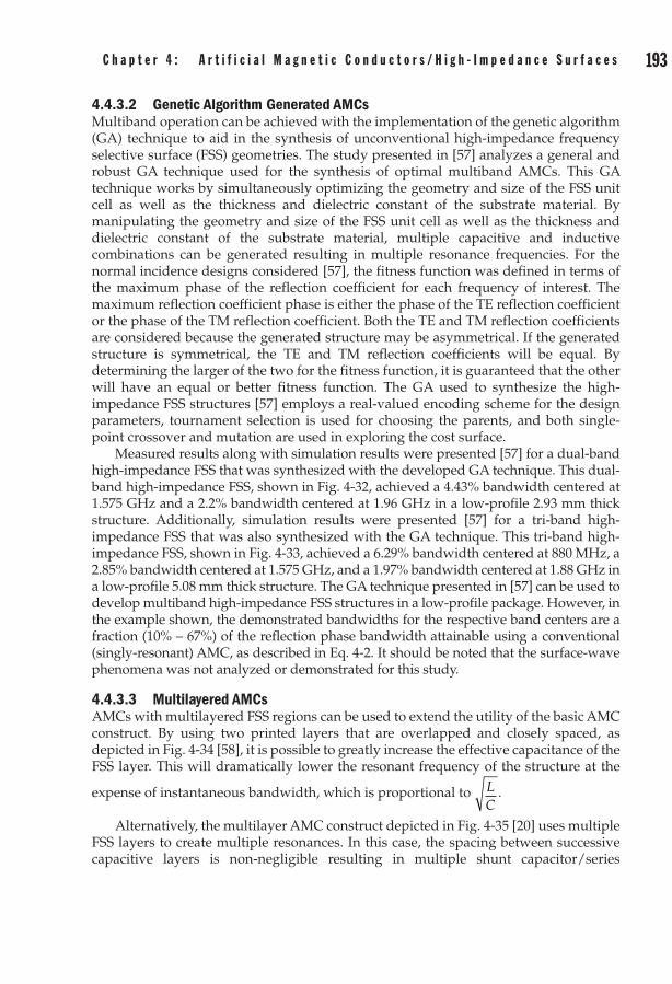
192 F r o n t i e r s i n A n t e n n a s : N e x t G e n e r a t i o n D e s i g n & E n g i n e e r i n g C h a p t e r 4 : A r t i f i c i a l M a g n e t i c C o n d u c t o r s / H i g h - I m p e d a n c e S u r f a c e s 193
4.4.3.2 Genetic Algorithm Generated AMCsMultiband operation can be achieved with the implementation of the genetic algorithm (GA) technique to aid in the synthesis of unconventional high-impedance frequency selective surface (FSS) geometries. The study presented in [57] analyzes a general and robust GA technique used for the synthesis of optimal multiband AMCs. This GA technique works by simultaneously optimizing the geometry and size of the FSS unit cell as well as the thickness and dielectric constant of the substrate material. By manipulating the geometry and size of the FSS unit cell as well as the thickness and dielectric constant of the substrate material, multiple capacitive and inductive combinations can be generated resulting in multiple resonance frequencies. For the normal incidence designs considered [57], the fitness function was defined in terms of the maximum phase of the reflection coefficient for each frequency of interest. The maximum reflection coefficient phase is either the phase of the TE reflection coefficient or the phase of the TM reflection coefficient. Both the TE and TM reflection coefficients are considered because the generated structure may be asymmetrical. If the generated structure is symmetrical, the TE and TM reflection coefficients will be equal. By determining the larger of the two for the fitness function, it is guaranteed that the other will have an equal or better fitness function. The GA used to synthesize the high-impedance FSS structures [57] employs a real-valued encoding scheme for the design parameters, tournament selection is used for choosing the parents, and both single-point crossover and mutation are used in exploring the cost surface.
Measured results along with simulation results were presented [57] for a dual-band high-impedance FSS that was synthesized with the developed GA technique. This dual-band high-impedance FSS, shown in Fig. 4-32, achieved a 4.43% bandwidth centered at 1.575 GHz and a 2.2% bandwidth centered at 1.96 GHz in a low-profile 2.93 mm thick structure. Additionally, simulation results were presented [57] for a tri-band high-impedance FSS that was also synthesized with the GA technique. This tri-band high-impedance FSS, shown in Fig. 4-33, achieved a 6.29% bandwidth centered at 880 MHz, a 2.85% bandwidth centered at 1.575 GHz, and a 1.97% bandwidth centered at 1.88 GHz in a low-profile 5.08 mm thick structure. The GA technique presented in [57] can be used to develop multiband high-impedance FSS structures in a low-profile package. However, in the example shown, the demonstrated bandwidths for the respective band centers are a fraction (10% – 67%) of the reflection phase bandwidth attainable using a conventional (singly-resonant) AMC, as described in Eq. 4-2. It should be noted that the surface-wave phenomena was not analyzed or demonstrated for this study.
4.4.3.3 Multilayered AMCsAMCs with multilayered FSS regions can be used to extend the utility of the basic AMC construct. By using two printed layers that are overlapped and closely spaced, as depicted in Fig. 4-34 [58], it is possible to greatly increase the effective capacitance of the FSS layer. This will dramatically lower the resonant frequency of the structure at the
expense of instantaneous bandwidth, which is proportional to LC
.
Alternatively, the multilayer AMC construct depicted in Fig. 4-35 [20] uses multiple FSS layers to create multiple resonances. In this case, the spacing between successive capacitive layers is non-negligible resulting in multiple shunt capacitor/series
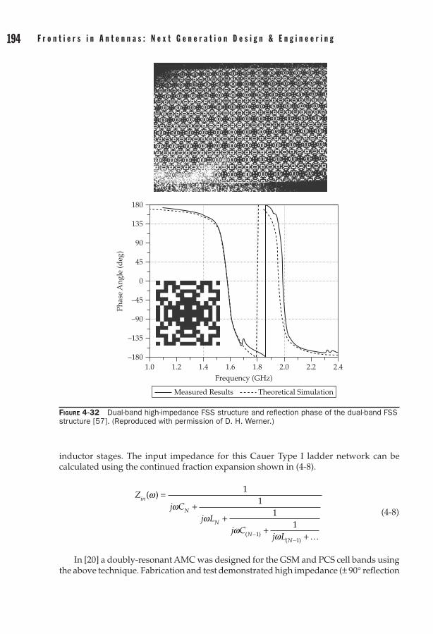
194 F r o n t i e r s i n A n t e n n a s : N e x t G e n e r a t i o n D e s i g n & E n g i n e e r i n g C h a p t e r 4 : A r t i f i c i a l M a g n e t i c C o n d u c t o r s / H i g h - I m p e d a n c e S u r f a c e s 195
inductor stages. The input impedance for this Cauer Type I ladder network can be calculated using the continued fraction expansion shown in (4-8).
Zj C
j Lj C
j L
in
N
N
NN
( )
( )( )
ωω
ωω
ω
=+
++
+--
11
11
11 K
(4-8)
In [20] a doubly-resonant AMC was designed for the GSM and PCS cell bands using the above technique. Fabrication and test demonstrated high impedance (± 90° reflection
Figure 4-32 Dual-band high-impedance FSS structure and reflection phase of the dual-band FSS structure [57]. (Reproduced with permission of D. H. Werner.)
180
135
90
45
0
–45
–90
–135
–180
Phas
e A
ngle
(deg
)
1.0 1.2 1.4 1.6Frequency (GHz)
1.8 2.0 2.2 2.4
Measured Results Theoretical Simulation

194 F r o n t i e r s i n A n t e n n a s : N e x t G e n e r a t i o n D e s i g n & E n g i n e e r i n g C h a p t e r 4 : A r t i f i c i a l M a g n e t i c C o n d u c t o r s / H i g h - I m p e d a n c e S u r f a c e s 195
Figure 4-33 Tri-band high-impedance FSS structure and reflection phase of the tri-band FSS structure [57]. (Reproduced with permission of D. H. Werner.)
180
135
90
45
0
–45
–90
–135
–180
Phas
e A
ngle
(deg
)
0.50 0.75 1.00 1.25Frequency (GHz)
1.50 1.75 2.00 2.25
CapacitanceCapacitanceLayer 1
Layer 2Figure 4-34 Three-layer AMC structure
Figure 4-35 Dual-band multilayered AMC [20]. (Reproduced with permission of W. E. McKinzie.)
d1
d2
t
tx
z
εr3
εr3
εr2
εr1
CapacitivePatches
FSS No. 1
FSS No. 2
Via

196 F r o n t i e r s i n A n t e n n a s : N e x t G e n e r a t i o n D e s i g n & E n g i n e e r i n g C h a p t e r 4 : A r t i f i c i a l M a g n e t i c C o n d u c t o r s / H i g h - I m p e d a n c e S u r f a c e s 197
phase response) in good agreement with the model. Through surface-wave coupling measurements, it was also demonstrated that this dual-band AMC exhibited a surface-wave band-gap over essentially the same frequency bands where the high surface impedance was observed (Fig. 4-36).
4.4.3.4 Negative Impedance AMCsThe approach presented in [59] entails the implementation of “negative” inductances and “negative” capacitances, which can be realized through the use of negative impedance converters (NICs) as detailed in Fig. 4-37, with the Sievenpiper AMC to widen the reflection phase bandwidth of the structure. An active two-port network that consists of an amplifier and a load impedance is configured in such a way as to provide
Figure 4-36 Measured reflection phase and TE and TM mode coupling [20]. (Reproduced with permission of W. E. McKinzie.)
15
10
5
0
–5
–10
–15
–20
–25
|S 1
2| (d
B)
500 1000
GSM 850 PCS 1900
1500 2000 2500
Frequency (MHz)
180
135
90
45
0
–45
–90
–135
–180
Ref
lect
ion
Phas
e (d
egre
es)
TM Mode CouplingTE Mode CouplingMeasured Reflection Phase
Figure 4-37 Negative impedance converter [59]. (Reproduced with permission of D. H. Werner.)
G
ZXZX
ZL
–ZLEs_
+
_
+
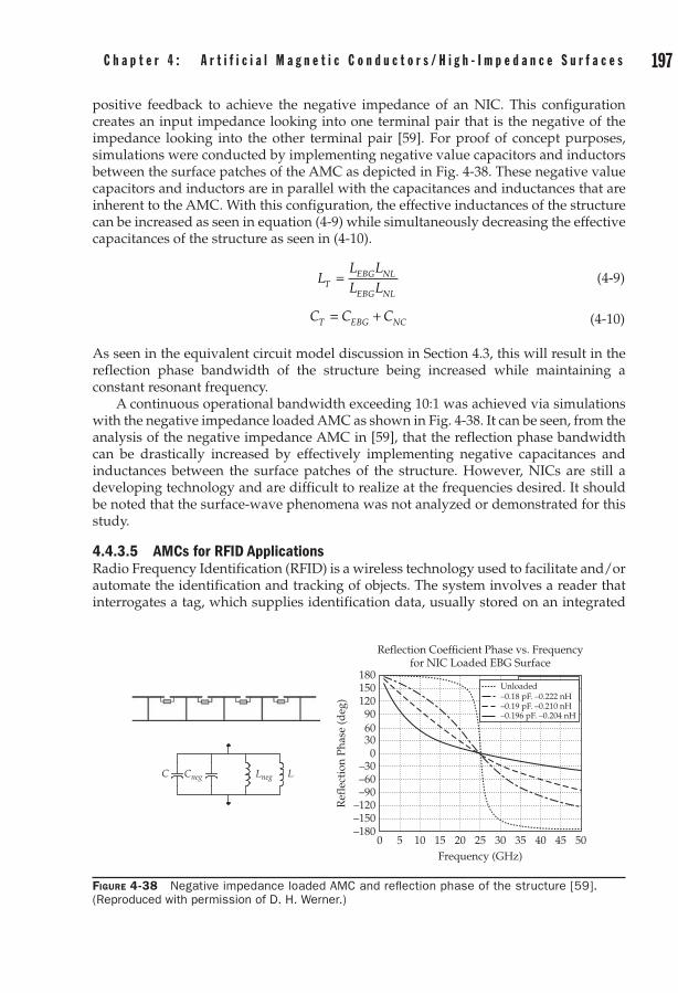
196 F r o n t i e r s i n A n t e n n a s : N e x t G e n e r a t i o n D e s i g n & E n g i n e e r i n g C h a p t e r 4 : A r t i f i c i a l M a g n e t i c C o n d u c t o r s / H i g h - I m p e d a n c e S u r f a c e s 197
positive feedback to achieve the negative impedance of an NIC. This configuration creates an input impedance looking into one terminal pair that is the negative of the impedance looking into the other terminal pair [59]. For proof of concept purposes, simulations were conducted by implementing negative value capacitors and inductors between the surface patches of the AMC as depicted in Fig. 4-38. These negative value capacitors and inductors are in parallel with the capacitances and inductances that are inherent to the AMC. With this configuration, the effective inductances of the structure can be increased as seen in equation (4-9) while simultaneously decreasing the effective capacitances of the structure as seen in (4-10).
LL LL LT
EBG NL
EBG NL
= (4-9)
C C CT EBG NC= + (4-10)
As seen in the equivalent circuit model discussion in Section 4.3, this will result in the reflection phase bandwidth of the structure being increased while maintaining a constant resonant frequency.
A continuous operational bandwidth exceeding 10:1 was achieved via simulations with the negative impedance loaded AMC as shown in Fig. 4-38. It can be seen, from the analysis of the negative impedance AMC in [59], that the reflection phase bandwidth can be drastically increased by effectively implementing negative capacitances and inductances between the surface patches of the structure. However, NICs are still a developing technology and are difficult to realize at the frequencies desired. It should be noted that the surface-wave phenomena was not analyzed or demonstrated for this study.
4.4.3.5 AMCs for RFID ApplicationsRadio Frequency Identification (RFID) is a wireless technology used to facilitate and/or automate the identification and tracking of objects. The system involves a reader that interrogates a tag, which supplies identification data, usually stored on an integrated
Figure 4-38 Negative impedance loaded AMC and reflection phase of the structure [59]. (Reproduced with permission of D. H. Werner.)
1801501209060300
–30–60–90
–120–150–180
0 5 10 15 20 25 30 35 40 45 50Frequency (GHz)
Ref
lect
ion
Phas
e (d
eg)
Reflection Coefficient Phase vs. Frequencyfor NIC Loaded EBG Surface
Unloaded–0.18 pF. –0.222 nH–0.19 pF. –0.210 nH–0.196 pF. –0.204 nH
LnegCneg LC

198 F r o n t i e r s i n A n t e n n a s : N e x t G e n e r a t i o n D e s i g n & E n g i n e e r i n g C h a p t e r 4 : A r t i f i c i a l M a g n e t i c C o n d u c t o r s / H i g h - I m p e d a n c e S u r f a c e s 199
circuit (IC) chip. Tags can be entirely passive, semi-active or active, with increasing complexity/cost and sampling range for the three technologies, respectively. In the passive case, energy from the interrogator powers the IC chip, which controls the termination impedance on the tag antenna to modulate the reflected energy. Tag design, particularly in the passive case, presents several challenging constraints. Good tags must be:
Small and/or low profile—so as to be minimally invasive appliqué to existing •packaging.
Low cost—because they are designed to be disposable.•
Efficient—in order to increase range for a given interrogator power/sensitivity.•
Insensitive to installation environment—so that it maintains its performance in •a variety of installation environments (atop a cardboard box, affixed to a plastic container of water, over metal, etc.).
Many of the RF tag antennas currently in use are loops or folded and/or meandered dipoles in various configurations [60], [61]. These designs tend to be very compact and cheap: however, many suffer from narrow impedance bandwidth and sensitivity to installation environment, particularly near conductors. Patches and PIFAs perform better in the metallic ground environment, but they still can suffer detuning related to ground plane size.
AMCs have the potential to remedy many of the performance limitations associated with these more conventional RFID antennas—at the expense of some degree of complexity. The high-impedance property allows a low-profile design while the surface-wave band-gap provides a mechanism for decoupling an antenna from its installation environment. The simplest implementation of an AMC for the RFID application is to incorporate an AMC backplane into the design of a meandered dipole or other small antenna and modulate the dipole load impedance in the conventional manner [62], [63]. This has been shown to provide an increase in the backscattered power relative to the non-AMC-backed case when in proximity to a metallic ground [64].
Another mechanism is to modulate the AMC surface itself, in a manner similar to that described in the previous section (Fig. 4-21). This method has the potential to provide significant improvements in tag performance for high-end semi-passive or active tags, providing polarization-independent backscatter with tailorable pattern and backscatter level related to modulation of the entire customizable surface [65].
ReferencesD. Sievenpiper, [1] High-Impedance Electromagnetic Surfaces, Ph. D. dissertation, University of California, Los Angeles, 1999.S. Rogers, J. Marsh, W. McKinzie, and J. Scott, “An AMC-based 802.11a/b antenna for laptop [2] computers,” IEEE Antennas and Propagation Society International Symposium, vol. 2, pp. 10–13, June 2003. L. C. Kretly, and S. Alves, “The effect of an electromagnetic band-gap structure on a PIFA antenna [3] array,” IEEE International Symposium on Personal, Indoor and Mobile Radio Communications, vol. 2, pp. 1268–1271, 2004.J. M. Bell, and M. F. Iskander, “A low-profile Archimedean spiral antenna using an EBG ground [4] plane,” IEEE Antennas and Wireless Propagation Letters, vol. 3, pp. 223–226, 2004.

198 F r o n t i e r s i n A n t e n n a s : N e x t G e n e r a t i o n D e s i g n & E n g i n e e r i n g C h a p t e r 4 : A r t i f i c i a l M a g n e t i c C o n d u c t o r s / H i g h - I m p e d a n c e S u r f a c e s 199
O. Luukkonen, C. Simovski, G. Granet, G. Goussetis, D. Lioubtchenko, A. V. Raisanen, and [5] S. A. Tretyakov, “Simple and accurate analytical model of planar grids and high-impedance surfaces comprising metal strips or patches,” IEEE Transactions on Antennas and Propagation, vol. 56, pp. 1624–1632, 2008.J. D. Joannopoulos, R. D. Meade, and J. N. Winn, Photonic Crystals—Molding the Flow of Light. [6] Princeton University Press, 1995.C. C. Cheng, A. Scherer, V. Arbet-Engels, and E. Yablonovitch, “3-D photonic crystals operating [7] at optical wavelengths,” Summaries of Papers Presented at the Quantum Electronics and Laser Science Conference, pp. 35–36, 1996. S. A. Clavijo, R. E. Diaz, and W. E. McKinzie “Design methodology for sievenpiper high-impedance [8] surfaces: An artificial magnetic conductor for positive gain electrically small antennas,” IEEE Trans. Antennas Propagt., vol. 51, pp. 2678–2690, Oct. 2003.S. A. Clavijo, and R. E. Diaz, “Simulation of the effective medium model (EMM) of the artificial [9] magnetic conductor (AMC) using the FDTD method [monopole antenna example],” IEEE Antennas and Propagation Society International Symposium, vol. 1A, pp. 164–167, 2005.D. Sievenpiper, L. Zhang, and E. Yablonovitch, “High-impedance electromagnetic ground planes,” [10] IEEE MTT-S International Microwave Symposium Digest, vol. 4, pp. 1529–532, 1999.J. Wong, and H. King, “A cavity-backed dipole antenna with wide-bandwidth characteristics,” [11] IEEE Transactions on Antennas and Propagation, vol. 21, pp. 725–727, 1973.A. D. MacDonald, “A modified Taguchi method for the design of broadband spiral cavity absorbers,” [12] IEEE Antennas and Propagation Society International Symposium, vol. 3, pp. 1180–1183, 1990.R. FitzGerrell, “The gain of a horizontal half-wave dipole over ground,” [13] IEEE Transactions on Antennas and Propagation, vol. 15, pp. 569–571, 1967.D. M. Pozar, “General relations for a phased array of printed antennas derived from infinite current [14] sheets,” IEEE Transactions on Antennas and Propagation, vol. 33, pp. 498–504, 1985.R. Mailloux, “On the use of metallized cavities in printed slot arrays with dielectric substrates,” [15] IEEE Transactions on Antennas and Propagation, vol. 35 , pp. 477–487, 1987.A. Oliner, and A. Hessel, “Guided waves on sinusoidally-modulated reactance surfaces,” IRE [16] Transactions on Antennas and Propagation, vol. 7, pp. 201–208, 1959.R. Elliott, “On the theory of corrugated plane surfaces,” [17] Transactions of the IRE Professional Group on Antennas and Propagation, vol. 2, pp. 71–81, 1954.R. King, D. Thiel, and K. Park, “The synthesis of surface reactance using an artificial dielectric,” [18] IEEE Transactions on Antennas and Propagation, vol. 31, pp. 471–476, 1983.R. M. Walser, A. P. Valanju, W. Win, M. F. Becker, R. W. Bene, A. B. Buckman, “New smart materials [19] for adaptive microwave signature control”, SPIE Vol. 1916, pp. 128–139, 1993W. McKinzie, and S. Rogers, “A multi-band artificial magnetic conductor comprised of multiple FSS [20] layers,” IEEE Antennas and Propagation Society International Symposium, vol. 2, pp. 423–426, 2003.D. J. Kern, D. H. Werner, and P. L. Werner,[21] “Optimization of multi-band AMC surfaces with magnetic loading,” IEEE Antennas and Propagation Society International Symposium, vol. 1, pp. 823–826, 2004.Z. Iluz, R. Shavit, and R. Bauer,[22] “Microstrip antenna phased array with electromagnetic bandgap substrate,” IEEE Transactions on Antennas and Propagation, vol. 52, pp. 1446–1453, 2004.W. E. McKinzie, R. B. Hurtado, B. K. Klimczak, and J. D. Dutton, “Mitigation of multipath through [23] the use of an artificial magnetic conductor for precision GPS surveying antennas,” IEEE Antennas and Propagation Society International Symposium, vol. 4, pp. 640–643, 2002.J. Ahn, C. Son, K. Chang, and Y. Yoon, “The miniaturization and electrical performance improvement [24] of base station array antenna with artificial magnetic conductor,” IEEE Antennas and Propagation Society International Symposium, vol. 1, pp. 1–4, 2009.D. F. Sievenpiper,[25] “Forward and backward leaky wave radiation with large effective aperture from an electronically tunable textured surface,” IEEE Transactions on Antennas and Propagation, vol. 53, pp. 236–247, 2005.
[26] R. E. Collin, Foundations for Microwave Engineering. McGraw-Hill New York 1966.[27] Richard T. Remski, Analysis of Photonic Bandgap Surfaces Using Ansoft HFSS, http://www.ansoft.com.[28] P. Kovacs, and Z. Raida, “Dispersion analysis of planar metallo-dielectric EBG structures in Ansoft
HFSS,” 17th International Conference on Microwaves, Radar and Wireless Communications, pp. 1–4, 2008.
[29] O. Folayan, and R. Langley, “Compact EBG antenna,” First European Conference on Antennas and Propagation, pp. 1–4, 2006.
[30] M. Salah Toubet, R. Chantalat, M. Thevenot, T. Monediere, and B. Jecko, “Conception of a low-profile and high-gain EBG resonator antenna with wide bandwidth,” International Workshop on Antenna Technology (iWAT), pp. 1–4, 2010.

200 F r o n t i e r s i n A n t e n n a s : N e x t G e n e r a t i o n D e s i g n & E n g i n e e r i n g C h a p t e r 4 : A r t i f i c i a l M a g n e t i c C o n d u c t o r s / H i g h - I m p e d a n c e S u r f a c e s 201
[31] J. Smit, and H. P. J. Wijn, Ferrites. New York: Wiley. & Sons, 1959.[32] R. Diaz, V. Sanchez, E. Caswell, and A. Miller, “Magnetic loading of artificial magnetic conductors
for bandwidth enhancement,” IEEE Antennas and Propagation Society International Symposium, vol. 2, pp. 431–434, June 2003.
[33] W. E. McKinzie III, R. E. Diaz, V. C. Sanchez, and E. Caswell, “Artificial magnetic conductor surfaces loaded with ferrite-based artificial magnetic materials,” United States Patent #7411565, August 2008.
[34] J. M. Bell, “Development of Metamaterials for Wideband Antenna Applications. Ph. D. dissertation, University of Hawaii, Manoa, 2008.
[35] J. J. Lee, S. Livingston, R. Koenig, D. Nagata, and L. L. Lai, “Compact light weight UHF arrays using long slot apertures,” IEEE Transactions on Antennas and Propagation, vol. 54, pp. 2009–2015, July 2006.
[36] A. Neto, and J. J. Lee, “Ultrawide-band properties of long slot arrays,” IEEE Transactions on Antennas and Propagation, vol. 54, pp. 534–543, February 2006.
[37] A. Neto, and J. J. Lee, “‘Infinite bandwidth’ Long Slot Array Antenna,” IEEE Antennas and Wireless Propagation Letters, vol. 4, pp. 75–78, 2005.
[38] IEEE Standard 1128–1998, IEEE Recommended Practice for Radio-Frequency (RF) Absorber Evaluation in the Range of 30 MHz to 5 GHz, April 1998.
[39] V. C. Sanchez, W. E. McKinzie III, and R. E. Diaz, “Broadband antennas over electronically recon-figurable artificial magnetic conductor surfaces, Antenna Applications Symposium, September 2001.
[40] D. F. Sievenpiper, R. J. Harvey, G. Tangonan, R. Y. Loo, and J. H. Schaffner, “Tunable impedance surface”, U.S. Patent # 6,538,621, March 2003.
[41] W. E. McKinzie, V. C. Sanchez, M. Reed, and S. L. Garrett, “Reconfigurable artificial magnetic con-ductor”, U.S. Patent # 6,897,831, May 2005.
[42] J. H. Schaffner, R. Y. Loo, D. F. Sievenpiper, F. A. Dolezal, G. L. Tangonan, J. S. Colburn, J. J. Lynch, J. J. Lee, S. W. Livingston, R. J. Broas, and M. Wu, “Reconfigurable aperture antennas using RF MEMS switches for multi-octave tunability and beam steering,” IEEE Antennas and Propagation Society International Symposium, vol. 1, pp. 321–324, 2000.
[43] D. Sievenpiper, J. Schaffner, R. Loo, G. Tangonan, S. Ontiveros, and R. Harold, A tunable impedance surface performing as a reconfigurable beam steering reflector,” IEEE Transactions On Antennas and Propagation, no. 3, vol. 50, March 2002.
[44] M. G. Bray, and D. H. Werner, “A broadband open-sleeve dipole antenna mounted above a tunable EBG AMC ground plane,” IEEE Antennas and Propagation Society International Symposium, vol. 2, pp. 1147–1150, 2004.
[45] J. Liang, and H. Y. D Yang, “Reconfigurable patch antenna on a tunable EBG substrate,” IEEE Antennas and Propagation Society International Symposium, pp. 5219–5222, 2007.
[46] V. C. Sanchez, W. E. McKinzie III, and R. E. Diaz, “Broadband antennas over electronically recon-figurable artificial magnetic conductor surfaces,” U.S. Patent # 6,917,343, July 2005.
[47] M. G. Bray, and D. H. Werner, “A novel design approach for an independently tunable dual-band EBG AMC surface,” IEEE Antennas and Propagation Society International Symposium, vol. 1, pp. 289–292, 2004.
[48] V. C. Sanchez, and E. Paller, “A tunable artificial magnetic conductor using switched capacitance in a concentric overlapping geometry,” IEEE Antennas and Propagation Society International Symposium, vol. 2, pp. 439–442, 2003.
[49] G. M. Coutts, R. R. Mansour, and S. K. Chaudhuri, “Microelectromechanical systems tunable frequency-selective surfaces and electromagnetic-bandgap structures on rigid-flex substrates,” IEEE Transactions on Microwave Theory and Techniques, vol. 56, pp. 1737–1746, 2008.
[50] D. M. Kokotoff, E. B. El-Sharawy, and C. R. Birtcher, “The radiation characteristics of a ferrite-tuned cavity-backed slot antenna,” IEEE Antennas and Propagation Society International Symposium, vol. 1, pp. 556–559, 1995.
[51] W. E. McKinzie, V. C. Sanchez, “Mechanically reconfigurable artificial magnetic conductor”, U.S. Patent #6,690,327, February 2004.
[52] F. Costa, S. Talarico, A. Monorchio, and M. F. Valeri, An active AMC ground plane for tunable low-profile antennas, IEEE Antennas and Propagation Society International Symposium, pp. 1–4, 2008.
[53] J. S. Colburn, A. Lai, D. F. Sievenpiper, A. Bekaryan, B. H. Fong, J. J. Ottusch, and P. Tulythan, “Adaptive artificial impedance surface conformal antennas,” IEEE Antennas and Propagation Society International Symposium, pp. 1–4, 2009.
[54] D. F. Sievenpiper, J. H. Schaffner, H. J. Song, R. Y. Loo, and G. Tangonan, “Two-dimensional beam steering using an electrically tunable impedance surface,” IEEE Transactions on Antennas and Propagation, vol. 51 , pp. 2713–2722, 2003.

200 F r o n t i e r s i n A n t e n n a s : N e x t G e n e r a t i o n D e s i g n & E n g i n e e r i n g C h a p t e r 4 : A r t i f i c i a l M a g n e t i c C o n d u c t o r s / H i g h - I m p e d a n c e S u r f a c e s 201
[55] K. Chang, J. Ahn, and Y. J. Yoon, “Physically flat but electromagnetic parabolic surface using EBG structure with stepped reflection phase,” 3rd European Conference on Antennas and Propagation, pp. 2609–2612, 2009.
[56] I. Gallina, A. D. Villa, V. Galdi, V. Pierro, F. Capolino, S. Enoch, G. Tayeb, and G. Gerini, “Aperiodic-tiling-based mushroom-type high-impedance surfaces,” IEEE Antennas and Wireless Propagation Letters, vol. 7, pp. 54–57, 2008.
[57] D. J. Kern, D. H. Werner, A. Monorchio, L. Lanuzza, and M. J. Wilhelm, “The design synthesis of multiband artificial magnetic conductors using high impedance frequency selective surfaces,” IEEE Transactions on Antenna and Propagation, vol. 53, pp. 8–17, January 2005.
[58] D. Sievenpiper, L. Zhang, R. F. J. Broas, N. G. Alexopolous, and E. Yablonovitch, “High-impedance electromagnetic surfaces with a forbidden frequency band,” IEEE Transactions on Microwave Theory and Techniques, vol. 47, pp. 2059–2074, November 1999.
[59] D. J. Kern, D. H. Werner, and M. J. Wilhelm, “Active negative impedance loaded ebg structures for the realization of ultra-wideband artificial magnetic conductors,” IEEE Antennas and Propagation Society International Symposium, vol. 2, pp. 427–430, June 2003.
[60] C. T. Rodenbeck, “Planar miniature rfid antennas suitable for integration with batteries,” IEEE Transactions on Antennas and Propagation, vol. 54, pp. 3700–3706, 2006.
[61] G. Marrocco, A. Fonte, and F. Bardati, “Evolutionary design of miniaturized meander-line antennas for RFID applications,” IEEE Antennas and Propagation Society International Symposium, vol. 2, pp. 362–365, 2002.
[62] B. Gao, C. H. Cheng, M. M. F. Yuen, and R. D. Murch, “Low cost passive UHF RFID packaging with electromagnetic band gap (EBG) substrate for metal objects,” Electronic Components and Technology Conference, pp. 974–978, 2007.
[63] D. Kim, and Y. Junho, “Low-profile RFID tag antenna using compact AMC substrate for metallic objects,” IEEE Antennas and Wireless Propagation Letters, vol. 7, pp. 718–720, 2008.
[64] R. M. Mateos, J. M. Gonzalez, C. Craeye, and J. Romeu, “Backscattering measurement from a RFID tag based on artificial magnetic conductors,” Second European Conference on Antennas and Propagation, pp. 1–4, 2007.
[65] V. C. Sanchez, “Artificial Magnetic Conductors,” Tutorial Workshop, IEEE Radar Conference, pp. 26–29, Apr 2004.

This page intentionally left blank

Chapter 5Metamaterial antennas
Gokhan Mumcu, Kubilay Sertel, and John L. Volakis
5.1 IntroductionReducing antenna size and profile via traditional miniaturization methods (such as shorting pins [1], meandering [2], and dielectric loading [3]) often result in low radia-tion efficiencies, narrow bandwidth, and undesired radiation patterns. It is not there-fore surprising that strong interest exists in engineered materials (referred to as meta-materials) as a method to optimize or enhance antenna performance.
Metamaterials are typically constructed from periodic arrangements of available materials (isotropic or anisotropic dielectrics, magnetic materials, conductors, etc.) and exhibit electromagnetic properties not found in any of their bulk individual constitu-ents. Over the last decade, theory and practical applications of material mixtures and metamaterials at microwave frequencies became an extensive research area [4]. For ex-ample, ferrites [5], [6] loaded ferrites, and ferroelectrics [7] have been exploited for phase shifters [8], antenna miniaturization, and beam control. Periodic assemblies effectively supporting negative refraction indices (NRI) allowed for sub wavelength focusing and greater sensitivity for lens applications [9]–[11]. Likewise, printed circuit NRI realizations have been utilized to develop miniature RF devices such as phase shifters and antennas [12]–[14]. Forbidden propagation bands and controllable disper-sion properties of electromagnetic band gap (EBG) structures [15], [16] have also been employed for novel waveguide, resonator, and filter designs [12]–[14]. Strong resonanc-es provided by the defect mode EBG structures have been shown to transform small radiators into directive antennas [17], [18]. Their band gaps were further used as high impedance ground planes to improve antenna radiation properties such as gain, con-formability, and coupling reduction [19]–[22]. Likewise, composite substrates assembled from different dielectric materials were used to improve the performance of printed antennas [23].
An important application of metamaterials is to reduce wave velocity, or even re-verse it in some frequency regions to achieve an electrically small RF structure [12]–[14], [24]–[27]. In this context, mode diversity and higher order dispersion (K-w) curves of periodically layered anisotropic (and possibly ferrimagnetic) materials have recently been proposed for high-gain and miniature antenna applications [28], [29]. These aniso-tropic material arrangements, namely degenerate band edge (DBE) [30] and magnetic
203

204 F r o n t i e r s i n a n t e n n a s : N e x t G e n e r a t i o n D e s i g n & e n g i n e e r i n g C h a p t e r 5 : M e t a m a t e r i a l a n t e n n a s 205
photonic (MPC) crystals [31], split the conventional K-w curves of otherwise isotropic EBG structures into two branches. Mode coupling between the branches (via misaligned anisotropy) generates novel slow group velocity modes to be harnessed by directive and small antennas. Specifically, in contrast to the 2nd order relation at the regular band edges (RBEs) of EBGs, the K-w curve behavior of the DBE mode follows a 4th order polynomial relation. Likewise, MPCs can exhibit spectral asymmetry (i.e., w (K) ≠ w (-K)) and support 3rd order stationary inflection points (SIPs) within their propagation bands [32]. In volumetric layered media, these higher order K-w behaviors result in stronger slow-wave resonances to be harnessed in designing conformal high-gain an-tenna apertures [28], [29]. When such dispersion relations are realized on traditional microwave substrates via printed coupled line emulations, they offer additional design flexibility to enable miniaturization, higher gain, and higher bandwidth [33], [34].
In this chapter, we present an overview of NRI and DBE based antennas. First, the novel propagation properties found in NRI metamaterials are described using their equivalent transmission line (TL) circuit models [13], [14]. Subsequently, antenna ex-amples from the recent literature are presented to demonstrate how NRI properties lead to novel and smaller antennas. Examples of high-gain antennas taking advantage of EBG structures are also presented.
The second half of the chapter is devoted to high-gain and small footprint anten-nas harnessing the DBE and MPC modes. We demonstrate that small antennas em-bedded in MPC and DBE crystals are converted into directive radiators due to the higher order K-w resonances. We also introduce printed line and lumped circuit con-figurations that can emulate DBE and MPC dispersion on traditional microwave sub-strates. Subsequently, a number of small printed antennas are presented by utilizing the mode diversity of layered anisotropic media. Specifically, we demonstrate that DBE and MPC antennas printed on high contrast substrates perform best among re-cently introduced metamaterial-based antennas in terms of their small gain × band-width product. We conclude by noting two particular near future application areas of small footprint metamaterial antennas: platform/vehicle integration and wideband arrays.
5.2 Negative Refractive Index (NRI) MetamaterialsIn the 1960s, Veselago was the first to examine media having negative dielectric (e) and magnetic (m) constitutive parameters (e < 0, m < 0) [35] In such media, electric (E) and magnetic fields (H) of plane waves along with the wavevector (k) form a “left-handed” (LH) triad. As such, the group (vg) and phase (vp) velocities have opposite directions. As usual, vg coincides with the direction of the pointing vector, S, and implies energy trans-fer away from the source to infinity in spite of the reversed phase velocity. That is, the media support backward wave propagation, but forward energy flow. This LH behav-ior is associated with the reversal of Snell’s law and implies a negative index of refrac-tion (n < 0) with reversed (negative) refraction angle. A comprehensive discussion on the properties and electromagnetic theory of NRI (e < 0, m < 0) media can be found in recently published books [13], [14].
Naturally, available materials do not exhibit simultaneously negative dielectric and magnetic constitutive relations. Methodologies to “artificially” realize such effective media (using periodic material inclusions) have been recently developed. For instance, at certain microwave frequencies, periodic arrangements of split ring resonators (SRRs)

204 F r o n t i e r s i n A n t e n n a s : N e x t G e n e r a t i o n D e s i g n & E n g i n e e r i n g C h a p t e r 5 : M e t a m a t e r i a l A n t e n n a s 205
and metallic thin wires were shown to exhibit negative permeability and permittivity, respectively [9], [10]. Another common method is to employ reactively loaded periodic TL grids [13], [14]. As compared to the resonator-based NRI structures, loaded one- dimensional (1D) and two-dimensional (2D) TLs exhibit broader bandwidth and can be conveniently realized using standard microstrip fabrication techniques. As a result, the concept of NRI-TLs found applications in various printed antenna and RF device de-signs (such as subwavelength focusing [11], phase shifters [12], couplers [14], miniature [25]–[27] and leaky-wave antennas [36]).
In general, a standard lossless TL can be modeled as a periodic structure with its unit cell (smallest element of periodicity) consisting of a circuit having series induc-tance and shunt capacitance. This circuit is assumed to represent a small section of the TL, much less than lg/4 (lg= guided wavelength). For an NRI TL, the circuit model re-lies on flipping the inductor and capacitor locations. However, in practical implementa-tions, the reactive loads responsible for the NRI effects must be placed within an ordi-nary host TL or material. Due to the parasitic effects of the host medium, NRI metamaterials also support ordinary right- handed (RH) wave propagation at higher frequencies. Therefore, the complete circuit model for the NRI-TL (see Fig. 5-1) includes distinct sets of reactive loads to represent both LH and RH propagation. For this reason, the NRI-TL circuit model is also referred to as the “composite right left-handed” (CRLH) metamaterial unit cell. As can be surmised from Fig. 5-1, the series CL and shunt LL ele-ments are responsible for LH propagation, whereas the shunt CR and series LR elements cause RH propagation at higher frequencies. Of course, the LH and RH propagation properties can be tuned to some desired frequency range by simply controlling the unit-cell parameters (i.e., amount of the reactive loads).
Wave propagation in one-dimensional periodic media can be effectively analyzed us-ing transfer matrix (T) formalism and making use of Bloch’s theorem (i.e., periodic boundary conditions) [37]. In accordance with Bloch’s theorem, electromagnetic fields propagat-ing along the z direction are first represented as a superposition of Bloch eigenmodes. Employing the periodic boundary condition (i.e., [ ( ) ( )] [ ( ) ( )]V z p I z p V z I z e+ + = −jkp, where p is the physical length of the unit cell and ejwt time dependence is assumed and sup-pressed) along with the definition of T matrix (i.e., [ ( ) ( )] [ ( ) ( )]V z I z V z p I z pT T= + +T leads to the eigenvalue equation [ ][ ( ) ( )]T I− =e V z I z Tjkp 0. ejkp can be now identified as the eigenvalue of T, having unity magnitude (i.e., k real) for propagating waves. We also
I1 = I(z) I2 = I(z)
LR CL
CRLLV1 = V(z) V2 = V(z+p)
+
–
+
–
0
Δz = p
Figure 5-1 Complete circuit model of NRI-TL media

206 F r o n t i e r s i n a n t e n n a s : N e x t G e n e r a t i o n D e s i g n & e n g i n e e r i n g C h a p t e r 5 : M e t a m a t e r i a l a n t e n n a s 207
remark that non-unity magnitude eigenvalues are associated with evanescent modes. Fur-ther, the equation leads to the same eigenvectors for k and k n p+ 2π / , n = ±1, ±2, ±3…. Thus, it is convenient to restrict k within the range - < <π π/ /p k p without loss of information. This region is referred to as the first Brillouin zone, and the eigenvalues are represented by the Bloch wavenumber K = kp in the horizontal axis, scaled from -p to p.
Using the above formalism, the dispersion relation of the NRI-TL is given by
K = -
-cos 1 12χ
, in which χωω
ωω
ω α=
+
-L
RL
2 2
2 , α = +L C L CR L L R, and ωL L LL C= 1 ,
ωR R RL C= 1 are the resonance frequencies of the loads responsible for LH and RH
behaviors, respectively. Likewise, ωse = 1 L CR L and ωsh = 1 L CL R denote the reso-
nance frequencies of the series and shunt loads. Figure 5-2a gives a representative K-w diagram in the 0 – 10 GHz band computed for LL = LR = 1 nH, CL = 3 pF, and CR = 1 pF. As seen, the circuit acts as a LH medium in the frequency range 1.27 GHz to 2.91 GHz by supporting opposite group and phase velocities. Between 2.91 GHz and 5.03 GHz no propagation occurs (band gap), and above 5.03 GHz the circuit behaves as a RH TL.
It can be shown that the K = 0 frequencies defining the upper and lower frequencies of the band-gap are equal to wse and wsh [14]. Thus, it is possible to remove the band gap completely (to obtain a continuous propagation band around the K = 0 frequency) by equating the series and shunt resonance frequencies, viz. by setting wse = wsh. Such NRI-TL (or CRLH) structures are referred to as “balanced” TLs and satisfy the load condition LR CL = LL CR. It is interesting to observe that the dispersion relation of balanced NRI-TLs can further be simplified to read K L C L CR R L L= -ω ω1/ around the K = 0 frequency
with the modes having corresponding impedances Z Z L C Z L CL L L R R R= = = = . In this case, the overall phase attained through the unit cell is simply the sum of positive and negative phases of the distinct RH and LH sections (as expected from the composite structure). To illustrate the concept of balanced NRI-TLs, an example dispersion diagram (computed for LR = 3 nH, LL = 1 nH, CL = 1 pF, and CR = 3 pF) is shown in Fig. 5-2b.
Figure 5-2 K-w diagram of the NRI Unit Cell shown in Fig. 5-1 with the Parameter Values (a) LL =
LR = 1 nH, C
L = 3 pF, and C
R = 1 pF; (b) L
R = 3 nH, L
L = 1 nH, C
L = 1pF, and C
R = 3 pF
10 5
4
3
2
1
0
8
6
4
2
0–π π
K–Bloch Wavenumber K–Bloch Wavenumber
Band gap
ωse
ωsh
ωsh = ωse
RHpropagation
RH
LHpropagation
LH
Freq
uenc
y (G
Hz)
Freq
uenc
y (G
Hz)
π/40 π/2 3π/4–π/4–π/2–3π/4 –π ππ/40 π/2 3π/4–π/4–π/2–3π/4
(a) (b)

206 F r o n t i e r s i n a n t e n n a s : N e x t G e n e r a t i o n D e s i g n & e n g i n e e r i n g C h a p t e r 5 : M e t a m a t e r i a l a n t e n n a s 207
5.3 Metamaterial Antennas Based on NRI ConceptsThe unit-cell model of the NRI metamaterials offers design flexibilities to reduce the operational frequency by employing reactive loads within the regular TL. Also, NRI metamaterials can conveniently exhibit multiple modes (in the LH and RH regime) when a finite number of unit cells is used to form microwave resonators. As such, print-ed NRI metamaterials were extensively studied to realize a variety of miniature and multiband antennas over the recent years. Further, the backward and forward waves realized on printed NRI metamaterials were found especially attractive to realize back-fire to end-fire scanning leaky-wave antennas (LWA) [36], [38].
5.3.1 Leaky-Wave Antennas (LWAs)For LWAs, guided power gradually leaks away in the form of coherent radiation as it propagates along the periodic waveguide structure (see Fig. 5-3a) [39]. In general, the rate of energy leakage is small along the waveguide and therefore the guided mode is not much perturbed. LWAs take advantage of this mechanism to achieve a desirable radiating structure exhibiting high gain, broadband impedance matching, and pattern scanning with frequency. As shown in Fig. 5-3a, the attenuation constant a is responsi-ble for the radiation over the aperture, whereas the wavenumber b (smaller than the free-space wavenumber k0) defines the direction of radiation. By ensuring that minimal amount of the traveling wave reaches the antenna end (employing a long antenna struc-ture), the LWA can exhibit broadband impedance match. Also, the LWA radiation pat-terns can be conveniently scanned with frequency over a large bandwidth due to the frequency dependent propagation constant.
The K-w diagram for a typical NRI-LWA is shown in Fig. 5-3b. The radiating region (i.e., K = Kx< K0) is bounded by the light lines (K0 = k0 p). Since the LH waves at lower frequencies (2.5 GHz to 2.91 GHz) exhibit K < 0 for +x propagating modes (i.e., vg > 0), the LWA radiates in the backward (i.e., -x) direction. On the other hand, the LWA radiates forward direction (i.e., +x) when the operational frequency is in the higher RH band (5.03 GHz to 10.6 GHz). As expected, the LWA seizes to radiate from 2.91 GHz to 5.03 GHz
Figure 5-3 (a) Operation Principle of LWAs. (b) K-w Diagram of the NRI-TL Forming the LWA for LL =
LR = 1 nH, C
L = 3 pF, C
R = 1 pF and Assumed Periodicity p = 1 cm. Light line is defined by K = k
0p.
π/2-θβ
k0kz
K–Bloch Wavenumber
Guided (Slow) Waves
−π −3π/4 −π/2−π/4 0 π/4 π/2 3π/4 π
Freq
uenc
y (G
Hz)
Radiating (Fast) Waves
RH band
Light lineLH bandInputRF
Printed Leaky-Wave Antenna (LWA)
ze−αx
Attenuation due toradiation leakage
Far field pattern(fan beam for 1D LWA)
β< k0x
(a) (b)
12
10
8
6
4
2
0
θ

208 F r o n t i e r s i n a n t e n n a s : N e x t G e n e r a t i o n D e s i g n & e n g i n e e r i n g C h a p t e r 5 : M e t a m a t e r i a l a n t e n n a s 209
due to the band gap. An important property of the NRI-LWAs is their capability to scan from backward to forward directions. In addition, a continuous backward to forward scan via frequency can be achieved when a balanced NRI-TL is employed [38].
One of the earliest printed layouts used to realize artificial NRI-TLs is shown in Fig. 5-4a [36]. As seen, a unique aspect of the NRI-TL is the interdigital capacitors and shorted inductive stubs formed along its path. These serve to slow down the wave and realize LH propagation. As noted, the reactive loading realized with interdigital capacitor and shorted microstrip stub gives rise to the LH behavior, and the parasitic effects due to metallization realize the RH behavior. The LWA in [36] consisted of N = 24 unit cells and operated from 3.1 GHz to 6.3 GHz, implying 61% bandwidth. The transition from LH to RH behavior (i.e., K = 0 point) occurred at 3.9 GHz. This structure was reported to exhibit more than 40% radiation efficiency with gain values above 6 dB (>10 dB sidelobe level) over the operational bandwidth. Figure 5-4b gives the measured E-plane radiation pat-terns, showing the backward to forward scan as the operating frequency is increased.
A variety of printed circuit realizations of the NRI-TL circuit were proposed for dif-ferent RF applications and needs. For instance, to obtain pattern scanning at a fixed frequency (in contrast to frequency dependent scanning), the NRI-TL unit cell was re-designed to incorporate varactor diodes as shown in Fig. 5-5 [40]. Conceptually, the bias voltages of the varactor diodes (3 per unit cell) are used to shift the dispersion diagram around the same operational frequency (w0) to create an electrically controllable K-w diagram. This implies different propagation constants (b) for each bias setting at the same w0. Thus, the LWA pattern is steered toward the angle sin-1(b/k0) as illustrated in Fig. 5-3a. The LWA shown in Fig. 5-5 consisted of N = 30 unit cells and was reported to allow scanning from -500 to +500 at 3.33 GHz as the varactor bias was varied from 0 V to 21 V. The observed maximum gain at broadside was around 18 dB.
Figure 5-6a displays another implementation employing coplanar strip (CPS) tech-nology for removing the need of via holes. The CPS NRI-TL unit cell (see Fig. 5-6b) was employed to develop a one-dimensional LWA with reduced beam squinting [41]. By adjusting the slope and shape of the K-w diagram, the LWA shown in Fig. 5-6a was de-signed to achieve 560 scanning over 1.8 GHz bandwidth, implying an average beam squint of 0.0310/MHz. At the center frequency (5 GHz), the LWA was adjusted to radi-ate toward 450. Among other LWA realizations, we note the amplifier-loaded NRI-LWA (for achieving arbitrary gain levels) in [42], the dielectric resonator-based configuration (for mitigating losses associated with conductors) in [43], and the two-dimensional NRI-TL LWA in [44].
5.3.2 Miniature and Multiband Patch AntennasSimilar to conventional resonators, the ones based on NRI-TL unit cells must be multi-ples of half wavelength (i.e., ℓ = nlg/2 → b = np). Therefore, resonant modes of an N unit cell NRI-TL occurs at K = pn/N frequencies (n being an integer smaller than N). As illus-trated in Fig. 5-7a, the LH branch of the NRI-TL allows for negative resonances (n < 0) whereas the RH branch gives rise to the traditional (n > 0) resonances. Since the dual resonances (± n) exhibit similar field distributions and impedance characteristics (due to the identical K magnitude), the NRI-TL structures were exploited for a variety of multiband antennas. Also, NRI-TL structures provide a convenient antenna miniatur-ization technique as their unit cells can be kept electrically small by employing inter-digital or lumped reactive circuit elements. An interesting situation relates to the zeroth-order resonance (n = 0) as the operational frequency at K = 0 becomes indepen-dent of the overall antenna physical length. In this case, to improve radiation efficiency

208 F r o n t i e r s i n a n t e n n a s : N e x t G e n e r a t i o n D e s i g n & e n g i n e e r i n g C h a p t e r 5 : M e t a m a t e r i a l a n t e n n a s 209
Figure 5-4 (a) Microstrip implementation of NRI-TL unit cell. (b) Radiation patterns of N = 24 unit cell one-dimensional NRI-LWA. Unit cells have the layout shown above (after Liu et al. [36], © IEEE 2002).
3.4 GHz 3.9 GHz
4.3 GHz
SimulationMeasurement
300
330
0
30
6090
120
150
180
210
240270
300
330
0
30
6090
120
150
180
210
240270
300
330
0
30
6090
120
150
180
210
240270
0
–10
–20
–30
–40
–50
–60
0
–10
–20
–30
–40
–50
–60
0
–10
–20
–30
–40
–50
–60
Interdigital Capacitor
LR/2 LR/22CL 2CL
Shorted Stub
Unit cell
(a)
(b)
p
LL CR

210 F r o n t i e r s i n a n t e n n a s : N e x t G e n e r a t i o n D e s i g n & e n g i n e e r i n g C h a p t e r 5 : M e t a m a t e r i a l a n t e n n a s 211
Figure 5-5 LWA consisting of N = 30 varactor diode loaded microstrip NRI-TL unit cells. The bias voltage of the varactors is used to vary the dispersion diagram as illustrated below. Various radiation patterns are obtained at a fixed w
0 by controlling the b values (after Lim et al. [40], ©
IEEE 2005).
ω0
V1
V1
V2
V2
V3
V3 ω = +cβ
(β = k0)
β = 0 βRH > 0 βLH < 0 β/k0
ω
GND, Vb (–)
DC bias Vb(+)
ViaVia
Series varactors
Shunt varactorx
z
y
+
+
–
+–
Port 2
ZL
Inductor (DC Feed)
3.02 cm (0.46λeff )µstrip
d = 1.2 cm (0.18λeff )µstrip
E-FieldUnit cell
Port 1
Pin
38.34 cm (5.87λeff )µstrip
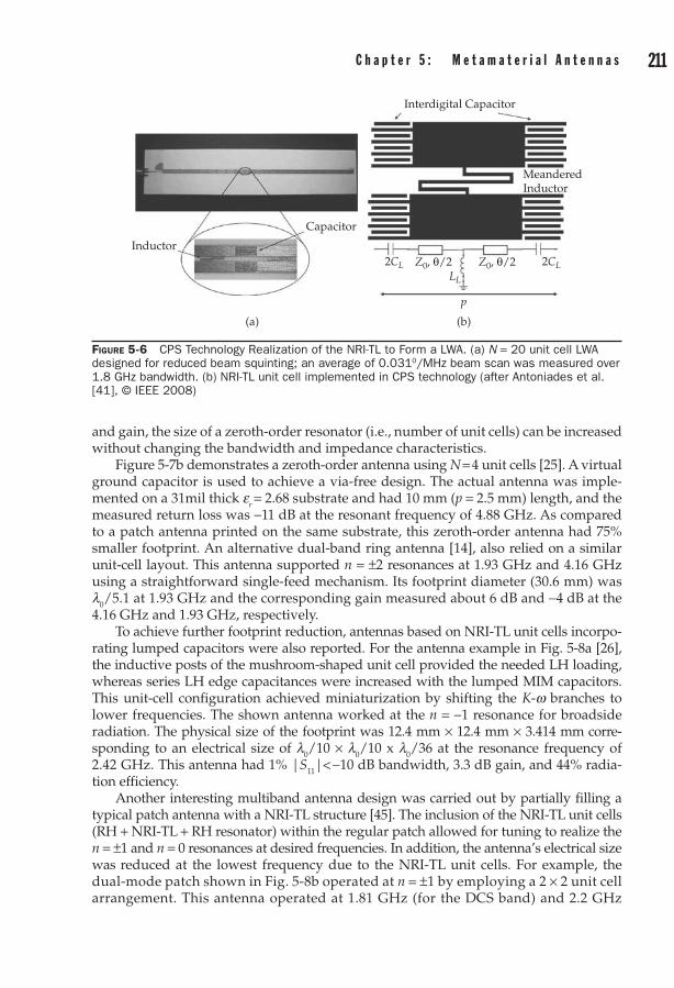
210 F r o n t i e r s i n a n t e n n a s : N e x t G e n e r a t i o n D e s i g n & e n g i n e e r i n g C h a p t e r 5 : M e t a m a t e r i a l a n t e n n a s 211
Figure 5-6 CPS Technology Realization of the NRI-TL to Form a LWA. (a) N = 20 unit cell LWA designed for reduced beam squinting; an average of 0.0310/MHz beam scan was measured over 1.8 GHz bandwidth. (b) NRI-TL unit cell implemented in CPS technology (after Antoniades et al. [41], © IEEE 2008)
Inductor
Capacitor
(a)
Interdigital Capacitor
MeanderedInductor
(b)
2CL 2CLLL
p
Z0, θ/2 Z0, θ/2
and gain, the size of a zeroth-order resonator (i.e., number of unit cells) can be increased without changing the bandwidth and impedance characteristics.
Figure 5-7b demonstrates a zeroth-order antenna using N = 4 unit cells [25]. A virtual ground capacitor is used to achieve a via-free design. The actual antenna was imple-mented on a 31mil thick er = 2.68 substrate and had 10 mm (p = 2.5 mm) length, and the measured return loss was -11 dB at the resonant frequency of 4.88 GHz. As compared to a patch antenna printed on the same substrate, this zeroth-order antenna had 75% smaller footprint. An alternative dual-band ring antenna [14], also relied on a similar unit-cell layout. This antenna supported n = ±2 resonances at 1.93 GHz and 4.16 GHz using a straightforward single-feed mechanism. Its footprint diameter (30.6 mm) was l0/5.1 at 1.93 GHz and the corresponding gain measured about 6 dB and -4 dB at the 4.16 GHz and 1.93 GHz, respectively.
To achieve further footprint reduction, antennas based on NRI-TL unit cells incorpo-rating lumped capacitors were also reported. For the antenna example in Fig. 5-8a [26], the inductive posts of the mushroom-shaped unit cell provided the needed LH loading, whereas series LH edge capacitances were increased with the lumped MIM capacitors. This unit-cell configuration achieved miniaturization by shifting the K-w branches to lower frequencies. The shown antenna worked at the n = -1 resonance for broadside radiation. The physical size of the footprint was 12.4 mm × 12.4 mm × 3.414 mm corre-sponding to an electrical size of l0/10 × l0/10 x l0/36 at the resonance frequency of 2.42 GHz. This antenna had 1% |S11|< -10 dB bandwidth, 3.3 dB gain, and 44% radia-tion efficiency.
Another interesting multiband antenna design was carried out by partially filling a typical patch antenna with a NRI-TL structure [45]. The inclusion of the NRI-TL unit cells (RH + NRI-TL + RH resonator) within the regular patch allowed for tuning to realize the n = ±1 and n = 0 resonances at desired frequencies. In addition, the antenna’s electrical size was reduced at the lowest frequency due to the NRI-TL unit cells. For example, the dual-mode patch shown in Fig. 5-8b operated at n = ±1 by employing a 2 × 2 unit cell arrangement. This antenna operated at 1.81 GHz (for the DCS band) and 2.2 GHz

212 F r o n t i e r s i n a n t e n n a s : N e x t G e n e r a t i o n D e s i g n & e n g i n e e r i n g C h a p t e r 5 : M e t a m a t e r i a l a n t e n n a s 213
(for the UMTS band) with 7.2% and 5% |S11|< -6 dB bandwidths, respectively. The corresponding measured gain and efficiency were 4.5 dB and 60% for the n = -1 mode; 6.8 dB and 83% for the n = 1 mode. The associated antenna physical size (footprint) was 48.2 mm × 48.2 mm × 8 mm, implying an electrical length of l0/3.4 at the lowest resonance frequency.
5.3.3 Compact and Low-Profile Monopole AntennasNRI metamaterials have also been considered to design compact and low-profile elec-trically small monopole-like radiators. As depicted in Fig. 5-9a, a traditional monopole has a l0/4 height to achieve in-phase radiating currents. However, a low-profile mono-pole (see Fig. 5-9b) can be instead considered provided it is excited to support the com-mon mode. Since a compact footprint is also desired, the ~l/2 phase shifter required to bring the currents in-phase must be kept physically small. Using metamaterial based compact phase shifters, the monopoles can be made with smaller footprints and lower profiles.
Figure 5-7 (a) Resonant modes of an unbalanced N unit cell NRI-TL structure. (b) N = 4 unit cell zeroth-order NRI-TL antenna and its unit cell (after Sanada et al. [25], © IEEE 2004).
10
8
6
Freq
uenc
y (G
Hz)
4
2
0–π π
ω–(N–1)
ω+(N–1)
ω–2
ω–1
ω–0
ω+0
ω+1
ω+2
–(N – 1)πN
(N – 1)πN
–2πN
2πN
–πN
πN
K – Bloch Wavenumber
(a)
Interdigitalcapacitor
MeanderedInductor
VirtualGround
Capacitor
(b)Unit cell
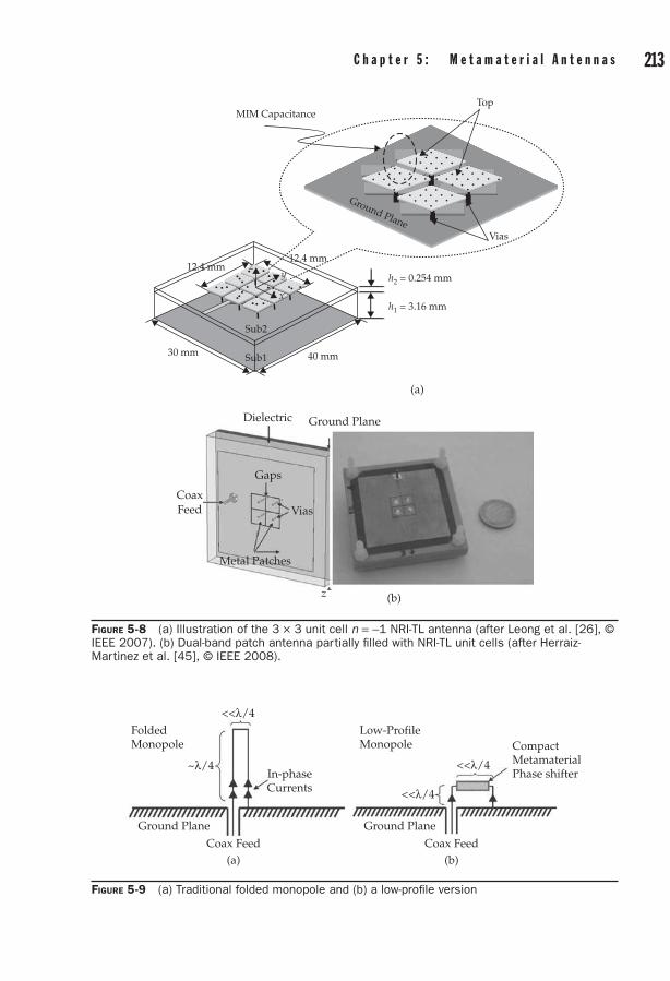
212 F r o n t i e r s i n a n t e n n a s : N e x t G e n e r a t i o n D e s i g n & e n g i n e e r i n g C h a p t e r 5 : M e t a m a t e r i a l a n t e n n a s 213
Figure 5-8 (a) Illustration of the 3 × 3 unit cell n = -1 NRI-TL antenna (after Leong et al. [26], © IEEE 2007). (b) Dual-band patch antenna partially filled with NRI-TL unit cells (after Herraiz-Martinez et al. [45], © IEEE 2008).
Dielectric
ViasCoaxFeed
z
Metal Patches
Ground Plane
(b)
Gaps
MIM CapacitanceTop
Vias
40 mm
(a)
Sub2
30 mm
zy
x
h2 = 0.254 mm
h1 = 3.16 mm
Ground Plane
12.4 mm12.4 mm
Sub1
Figure 5-9 (a) Traditional folded monopole and (b) a low-profile version
Coax Feed
In-phaseCurrents
<<λ/4
~λ/4
Ground Plane
FoldedMonopole
Coax Feed(a) (b)
CompactMetamaterialPhase shifter
<<λ/4
<<λ/4
Ground Plane
Low-ProfileMonopole
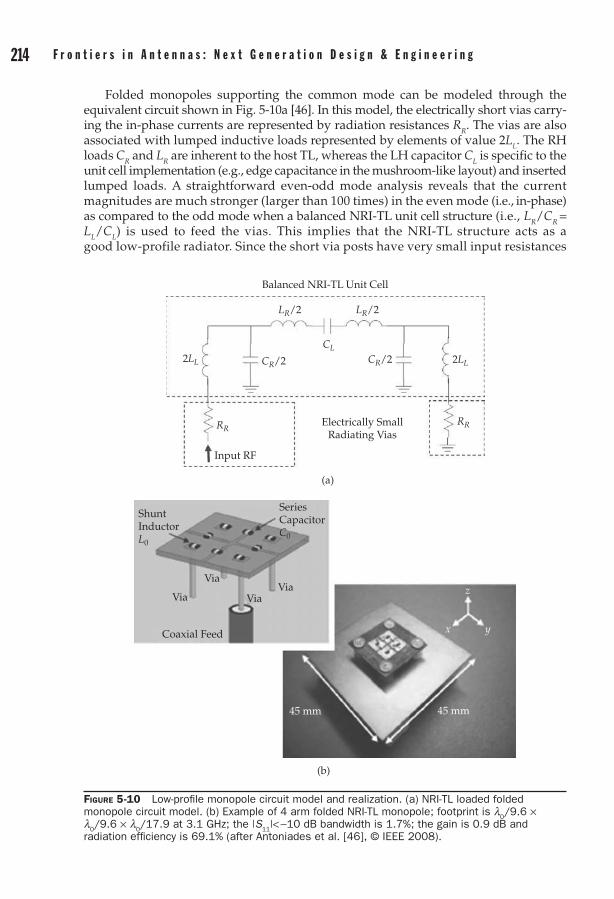
214 F r o n t i e r s i n a n t e n n a s : N e x t G e n e r a t i o n D e s i g n & e n g i n e e r i n g C h a p t e r 5 : M e t a m a t e r i a l a n t e n n a s 215
Figure 5-10 Low-profile monopole circuit model and realization. (a) NRI-TL loaded folded monopole circuit model. (b) Example of 4 arm folded NRI-TL monopole; footprint is l
0/9.6 ×
l0/9.6 × l
0/17.9 at 3.1 GHz; the |S
11|< -10 dB bandwidth is 1.7%; the gain is 0.9 dB and
radiation efficiency is 69.1% (after Antoniades et al. [46], © IEEE 2008).
Balanced NRI-TL Unit Cell
Electrically SmallRadiating Vias
(a)
2LL 2LLCR/2 CR/2CL
LR/2
RRRR
LR/2
Input RF
ShuntInductorL0
Coaxial Feed
(b)
Via
Via
Via
45 mm 45 mm
Via z
x y
SeriesCapacitorC0
Folded monopoles supporting the common mode can be modeled through the equivalent circuit shown in Fig. 5-10a [46]. In this model, the electrically short vias carry-ing the in-phase currents are represented by radiation resistances RR. The vias are also associated with lumped inductive loads represented by elements of value 2LL. The RH loads CR and LR are inherent to the host TL, whereas the LH capacitor CL is specific to the unit cell implementation (e.g., edge capacitance in the mushroom-like layout) and inserted lumped loads. A straightforward even-odd mode analysis reveals that the current magnitudes are much stronger (larger than 100 times) in the even mode (i.e., in-phase) as compared to the odd mode when a balanced NRI-TL unit cell structure (i.e., LR/CR = LL/CL) is used to feed the vias. This implies that the NRI-TL structure acts as a good low-profile radiator. Since the short via posts have very small input resistances

214 F r o n t i e r s i n a n t e n n a s : N e x t G e n e r a t i o n D e s i g n & e n g i n e e r i n g C h a p t e r 5 : M e t a m a t e r i a l a n t e n n a s 215
(i.e., RR = 160p2(h/l0)2, where h stands for height [47]), multiple (M) folded arms are
commonly employed to improve impedance matching through the relation Rin≈ M2RR [48]. Figure 5-10b demonstrates a compact and low-profile NRI-TL ring antenna consist-
ing of four unit cells [46]. For this, the footprint was 10 mm (l0/9.6) × 10 mm (l0/9.6) × 5.4 mm (l0/17.9) at the resonance frequency of 3.1 GHz. The corresponding measured |S11|< -10 dB bandwidth was reported to be 1.7% with 0.9 dB gain and 69.1% radiation efficiency. Another compact NRI-TL ring antenna shown in Fig. 5-11a realized a l0/11 × l0/13 × l0/28 footprint area at 1.77 GHz. The measured |S11|< -10 dB bandwidth was reported to be 6.8% with 0.95 dB gain and 54% radiation efficiency [27].
Alternatively, the low-profile monopoles introduced in [49] and [50] made use of compact 1800 phase shifters to achieve a common mode in low-profile monopole real-ization. Specifically, the antenna shown in Fig. 5-11b consisted of a standard TL connected to two shorting posts loaded with lumped inductors. The inductor choices of 10 nH and 5 nH resulted in a l0/4.9 × l0/45.6 × l0/12.2 footprint antenna, operating at 2.19 GHz. The antenna had 2.9 dB gain and 32% radiation efficiency with 4.7%
Figure 5-11 (a) Low-profile NRI-TL ring antenna consisting of 2 asymmetric unit cells, footprint is l
0/11 × l
0/13 × l
0/28 at 1.77 GHz. |S
11|< -10 dB bandwidth is 6.8%, gain is 0.95 dB, and
radiation efficiency is 54% (after Qureshi et al. [27], © IEEE 2005). (b) Inductor loaded antenna having footprint of l
0/4.9 × l
0/45.6 × l
0/12.2 at 2.19 GHz, |S
11|<-10 dB bandwidth is 4.7%,
gain is -2.9 dB, and radiation efficiency is 32% (after Lee et al. [49], © IEEE 2007). (c) Miniature antenna with embedded spiral loading; footprint is l
0/4.9 × l
0/45.6 × l
0/16 at 2.4 GHz. |S
11|< -10
dB bandwidth is 1% (after Kokkinos et al. [50], © IEEE 2007).
HoldingBrackets
Caps
Metal TL
14.8 mm
13.1 mm
Via
Feed
32 mil
6 mm
GroundPlane
(a)
Dielectric
2Lo2
2Lo1
InductorsL1 and L2
(b)
d2
d1
l1
l2
(y)
(x)(c)

216 F r o n t i e r s i n a n t e n n a s : N e x t G e n e r a t i o n D e s i g n & e n g i n e e r i n g C h a p t e r 5 : M e t a m a t e r i a l a n t e n n a s 217
|S11|< -10 dB bandwidth. Another monopole-like miniature antenna in Fig. 5-11c real-ized the 1800 phase shift using an embedded spiral. For this, the measured |S11|< -10 dB bandwidth was about 1% and the antenna footprint was l0/4.9 × l0/45.6 × l0/16 at about 2.4 GHz.
Among other compact and low-profile monopole realizations, we remark the NRI-TL based monopole with two nearby resonances (for bandwidth improvement) [51] and NRI-TL loaded wideband printed monopole antenna [52]. In addition, several elec-trically small antennas (with low radiation resistances) were placed in close proximity of a metamaterial (e.g., e < 0, or m < 0, or NRI) unit cells to form a self resonating an-tenna system [24], [53]. For example, a small rectangular loop antenna placed within close proximity of a parasitic capacitively loaded loop was shown to achieve 50Ω im-pedance match [53]. The antenna resonated at 438.1 MHz with a 0.43% |S11|< -10 dB bandwidth, and its dimensions (excluding the ground plane) were l0/9.4 × l0/18 × l0/867. Its corresponding computed gain was 4.8 dB with 79.5% efficiency. As another example, we mention the dipole antenna loaded with multiple SRRs to achieve multi-band operation at 1.3 GHz and 2.8 GHz [54].
5.4 High-Gain Antennas Utilizing EBG Defect ModesElectromagnetic bandgap structures (EBGs) are artificial periodic media that can pre-vent electromagnetic wave propagation in specified directions and frequency bands (e.g., see the band-gap regime of the one-dimensional NRI-TL medium previously shown in Fig. 5-2a). Depending on the structural complexity (i.e., one-, two-, or three-dimensional periodicity) and contrast difference of the constituent materials, EBGs can be designed to block propagation in single or multiple directions with relatively narrow or wide bandwidths [16]. Due to these exotic propagation properties and design flexi-bilities, EBGs have attracted considerable interest from the electromagnetic community since their initial introduction [15]. Consequently, EBGs have found a wide range of RF applications and have been successfully employed to enhance performance of vari-ous devices such as filters, waveguides, and antennas [16], [55], [56].
Figure 5-12 (a) Antenna placed inside a defect mode EBG made from alumina rods delivering 19 dB gain, 50% aperture efficiency (after Thevenot et al. [61], © IEEE 1999). (b) Woodpile EBG resonator fed by a double slot antenna operating near 12.5GHz. antenna has 19.8 dB gain, 63% radiation efficiency, and 19% aperture efficiency; EBG size: 6.3l
0 × 6.3l
0 × 0.49l
0 (after Weily
et al. [62], © IEEE 2005).
ϕ = 0ϕ = π/2
Dielectric AluminaRods (ε = 9.8)
258 mm 258 mm
22.36 mm
22.36 mm
21.2 mm
(a)
Metallic GroundPlane
Φ = 10.6 mm
33.54 mm
21.2 mm
Woodpile EBG Material
Metallic Ground Plane
(b)
Double Slot Antenna
yz
x
d2

216 F r o n t i e r s i n a n t e n n a s : N e x t G e n e r a t i o n D e s i g n & e n g i n e e r i n g C h a p t e r 5 : M e t a m a t e r i a l a n t e n n a s 217
EBGs are generally harnessed in several ways for antenna applications. For exam-ple, their band-gap feature can be utilized as a high impedance ground plane [19] to enhance radiation performance (gain, pattern, reduced side/back lobes, etc.) by suppressing undesired surface waves and mutual couplings. In addition, EBGs provide for in-phase reflection at their band-gap frequencies and form artificial magnetic ground planes that lead to low-profile antenna realizations [20].
An important characteristic of EBGs is their capability to support localized electro-magnetic modes within band-gap frequencies when defects are introduced in their periodic structure (e.g., by replacing one or several unit cells with a different material) [16]. These localized modes are associated with narrow transmission regimes occur-ring within the band-gap frequencies. Since transmission is sensitive to the propaga-tion direction, an antenna embedded within the defect can radiate to free space only in particular directions. Therefore, very high-gain levels can be obtained with simpler structures. This approach can be an alternative to two-dimensional antenna arrays re-quiring complex and lossy feed networks [17], [18], [57]–[59]. More specifically, [58] and [59] investigated directivity enhancements of a dipole or patch antenna placed under multiple layer dielectric slabs and explained the concept as a leaky wave [60]. Although the multilayered structure was not referred to as a defect mode EBG at that time, it can be considered as one of the earliest high-gain EBG antennas. The fact that small antennas embedded in defect mode EBGs get converted into directive radiators was experimentally demonstrated in [17]. Figure 5-12a demonstrates a patch antenna located inside a defect mode EBG [61]. The EBG was constructed from rows of dielec-tric (alumina) rods separated by air. When the separation between the ground plane and rods are properly adjusted (according to the reflection phase of the EBG super-strate), the overall structure can be considered as having four rows of rods: two above the ground plane and two below (as a consequence of image theory). The defect is cre-ated by enlarging the separation between the second and third rows (i.e., larger gap between the second row and ground plane). A l0/3 × l0/3 × l0/19.9 patch antenna placed in the defect area resonates at 4.75 GHz and delivers 19 dB gain (with an EBG size of 4.05l0 × 4.05l0 × 0.97l0) and 50% aperture efficiency. The gain bandwidth (fre-quency interval over which gain stays within 3 dB of the peak value) was 3% and a mini-mum |S11| of -8 dB was measured.
To provide more control over the radiation properties, it was proposed in [62] to em-ploy an EBG structure capable of exhibiting band gap in all propagation directions (i.e., three-dimensional). As depicted in Fig. 5-12b, a woodpile EBG was placed above a patch or double slot antenna to enhance directivity. We note that a 15.2 cm × 15.2 cm EBG aper-ture (with total antenna thickness of 11.7 mm and a ground plane size of 30 cm × 30 cm) was employed to maximize the directivity of the patch feed operating near 12.5 GHz. The authors found that the double slot antenna exhibits about 1 dB better gain than the patch at the expense of a more complex feed mechanism. The measured gain was 19.8 dB with 1% |S11|< -10 dB bandwidth. The structure had 63% radiation efficiency and 19% aperture efficiency.
Partially reflecting surfaces (PRS) or frequency selective surfaces (FSS) [63]–[65] are other alternatives of EBGs in forming resonator-based high-gain antennas. In such reso-nators, confined EM energy between PRS and ground plane gradually leaks away and thus, a large radiation aperture supporting high levels of directivity is realized. Since PRS exhibit a reflection coefficient near to -1, it must be placed about half wavelength (~l0/2) above the ground plane to form the resonator (see Fig. 5-13a). To lower the profile,

218 F r o n t i e r s i n a n t e n n a s : N e x t G e n e r a t i o n D e s i g n & e n g i n e e r i n g C h a p t e r 5 : M e t a m a t e r i a l a n t e n n a s 219
an approach is to replace the metallic ground plane with one that has a reflection coef-ficient near to +1. With this in mind, the paper in [66] proposed to employ an artificial magnetic ground plane (AMC) under the PRS. As shown in Fig. 5-13b, a patch antenna placed in the middle of the AMC excites the PRS-AMC cavity. For a simpler de-sign, the AMC was designed from a via-free unit-cell layout [67], [68] instead of a mush-room- like EBG structure. To form the cavity, the PRS in Fig. 5-13c was placed about a quarter wavelength (5.9 mm, 0.28l0) above the AMC. The patch resonated at about 14.2 GHz having an electrical length of 0.116l0 and 2% |S11|< -10 dB bandwidth. The size of the AMC metallization was 15 cm (7.1l0) × 15 cm (7.1l0), whereas the PRS had a 10.6 cm (5l0) × 10.6 cm (5l0) footprint. The measured directivity was 19.5 dB with a side lobe level below -15 dB.
We can state that EBG, PRS, or FSS can be used to increase gain as a consequence of their high Q resonance mechanisms. However, these antennas inherently suffer from narrow bandwidths (since high Q resonances are very sensitive to frequency varia-tions). On the other hand, multiband designs can be proposed to partially address the narrow bandwidth issue. For example, [69] proposed to insert an additional FSS surface inside a PRS-PEC resonator to create dual-band operation at two closely spaced frequen-cies (5.15 GHz and 5.7 GHz). To realize dual resonance at closely spaced frequencies, [69] employed a highly selective FSS surface built from Hilbert-curve inclusions [70]. Likewise, [71] presented a detailed analysis of directivity enhancements using two different FSS printed on different sides of a thin dielectric layer.
5.5 Antenna Miniaturization Using Dispersion Properties of Layered Anisotropic Media
A goal in any antenna miniaturization is to lower resonance frequency without increas-ing physical size. It is therefore essential to understand how resonances can be lowered via wave slowdown techniques. As an example, Fig. 5-14a considers a printed-loop antenna that can be thought of as a circularly periodic arrangement involving two unit cells (top and bottom half loops). The unit-cell band diagram in Fig. 5-14b (identical to a uniform TL) indicates two K-w branches corresponding to two waves propagating in
Figure 5-13 (a) Lowering the resonant cavity profile with PMC ground plane. (b) 15 cm (7.1l0) ×
15 cm (7.1l0) AMC with a patch antenna feed; (c) 10.6 cm (5l
0) × 10.6 cm (5l
0) footprint PRS
placed 5.9 mm (0.28l0) above the AMC. (c) The antenna resonated at 14.2 GHz with 2%
|S11
|< -10 dB bandwidth, 19.5 dB directivity, and < -15 dB sidelobe level (after Feresidis et al. [66], © IEEE 2005).
PEC
h ≈ λ/2h ≈ λ/4
PRS
ϕ1
ϕ2
SourcePMC PRS
Source(a) (b) (c)

218 F r o n t i e r s i n a n t e n n a s : N e x t G e n e r a t i o n D e s i g n & e n g i n e e r i n g C h a p t e r 5 : M e t a m a t e r i a l a n t e n n a s 219
opposite directions (K > 0 and K < 0). As seen, the lowest order resonance occurs at the K = ± p frequency and is associated with matching phases of the two propagating waves. Clearly, to lower the resonance frequency, it is necessary to bend the K-w curve as in Fig. 5-14c. This can be done by inserting reactive elements (capacitive or inductive) within the TL (loop path) and therefore cause wave slowdown [72]. Indeed, although the reso-nance frequency at the K = ± p points can be further pushed down with reactive loading, the parabolic relation still remains 2nd order, limiting the curvature slope at the band edge. However, degenerate band edge (DBE) resonances can exhibit 4th order, maxi-mally flat K-w behavior at band edge frequencies [30]. As illustrated in Fig. 5-14c, such maximally flat K-w curves push the resonances further down in frequency to enhance antenna miniaturization. The improved flexibility (i.e., bending) of the dispersion dia-gram can be also exploited to form tunable antennas having larger frequency sweep ranges.
Since DBE crystals are associated with a nonlinear K-w behavior (see Fig. 5-15a) realized with anisotropic material loadings, a narrow bandwidth performance is also inevitable. However, as depicted in Fig. 5-15b, inclusion of magnetic layers forms a mag-netic photonic crystal (MPC) [31], which can generate spectral asymmetry with stationary
Figure 5-14 Printed antenna miniaturization using DBE dispersion. (a) Simple printed-loop antenna. (b) Dispersion diagram of the unit cell forming the loop; resonances of this circularly periodic structure (2 unit cells) are marked by dots. (c) Bending of the K-w diagram to shift resonance to lower frequencies and magnified view of the dispersion diagram around the band edge (after Mumcu et al. [33], © IEEE 2009).
Unit Cell(Length λg/2)
CircularlyPeriodic
Arrangement
(a)K
ω
π–π(b)
Freq
uenc
y (G
Hz)
K
ω
π–π
Band gap
Bloch Wavenumber (K)
0 π/4 π/2 3π/4 π2.5
3
3.5
4
4.52nd order RBE
4th order DBE
LoopResonance
(c)

220 F r o n t i e r s i n a n t e n n a s : N e x t G e n e r a t i o n D e s i g n & e n g i n e e r i n g C h a p t e r 5 : M e t a m a t e r i a l a n t e n n a s 221
inflection points (SIPs) [32]. This creates a linear section in the K-w curve that brings wider bandwidth. Another design advantage offered by anisotropic media is their support for multiple resonant modes. As depicted in Fig. 5-15, anisotropy increases the overall number of K = p or K = 0 resonances by creating additional K-w branches. This mode diversity and concurrent tuning flexibility may play a key role in designing planar and small footprint antennas operating at multiple frequencies. The works in [73], [74] pro-posed printed TLs that emulate volumetric anisotropy using a pair of coupled TLs on an otherwise uniform substrate. This low cost approach to realize planar anisotropy is exploited later in designing miniature DBE and MPC-based antennas.
5.5.1 Realizing DBE and MPC Modes via Printed Circuit Emulation of Anisotropy
Anisotropic media, generally, support a pair of propagating waves propagating with separate phase velocities. It was demonstrated in [33], [73] that a pair of printed TLs is needed to support this pair of propagating waves and emulate anisotropy on an oth-erwise uniform substrate. As depicted in Fig. 5-16, each of these lines is thought of as carrying one polarization component of the electric field. Since two anisotropic dielec-tric layers (with misaligned permittivity tensors) are required for the simplest DBE unit cell, printed DBE layout utilizes a cascade of uncoupled and coupled dual-line sections. The uncoupled section with different line lengths emulates diagonal anisot-ropy by introducing a phase delay between the two propagating waves. Similarly, even–odd mode impedances and propagation constants on the coupled lines allow emulation of volumetric and planar anisotropy (i.e., nondiagonal anisotropy tensor). The microwave circuit is tuned to achieve the DBE mode by appropriately selecting the line widths and coupled line separations [73]. This can also be accommodated us-ing the equivalent circuit shown in Fig. 5-17 [75]. To emulate spectral asymmetry (needed for the MPC modes), a ferrite substrate section can additionally be placed under the coupled lines. Changing the bias of the ferrite adjusts the nonreciprocal cur-rent displacement and bends the K-w branch to exhibit the SIP behavior [74].
Figure 5-15 K-w diagram depicting multiple resonances found in layered anisotropic media that can be harnessed to design multiband antennas. (a) Lowest order K = p resonances in a DBE crystal (note that wavenumbers are folded into the 0 < K < 2p interval); frequency spacing between the resonances can be adjusted by controlling the anisotropic permittivity ratio and flatness of the DBE resonance. (b) MPC dispersion supporting an SIP; wider bandwidth is expected at SIP frequency (in comparison to DBE) due to the larger K-w slope with magnetic material inclusions in the medium supporting resonance.
2ππ Κ
ω
DBE
0 2ππ Κ
ω
SIP
0
Narrowbandwidth
Widerbandwidth
Multiple resonances dueto anisotropy
(a) (b)

220 F r o n t i e r s i n a n t e n n a s : N e x t G e n e r a t i o n D e s i g n & e n g i n e e r i n g C h a p t e r 5 : M e t a m a t e r i a l a n t e n n a s 221
To design a printed DBE unit cell (see Fig. 5-16) we proceed to tune the line lengths, widths, and coupling ratio using full wave numerical solutions. Unfortunately, an understanding of the various loading effects (i.e., capacitive vs. inductive) is not as easy due to the geometrical and computational challenges. Therefore we proceeded to develop an equivalent 4-port lumped circuit model to represent the DBE unit cells as
L1
L2
L3 LM
LM
LM
CMC1 C30 0
C300
C2 L3
Inductivecoupling
Capacitivecoupling
Coupled
(V3I3)
(V4I4)
(V1 I1)
(V2I2)
Uncoupled
(a) (b)
π/4 π/2 3π/4 2π3π/25π/4 7π/4π0
4.5
3.5
3
2.5
4
Freq
uenc
y (G
Hz)
Bloch Wavenumber (K)
CM = 2.3 pF,Degenerate Band Edge
CM = 4 pF,Double Band Edge
CM = 1 pF, Regular Band Edge
Figure 5-17 (a) Lumped circuit model of the printed DBE unit-cell layout. (b) Different band edges obtained simply by changing the amount of capacitive coupling C
M in case the uncoupled
section is capacitively loaded (L1 = L
2 = L
3 = 1 nH, C
1 = 10 pF, C
2 = C
3) (after Mumcu et al. [75] ©
IEEE 2009).
Figure 5-16 Concept of emulating anisotropy on a printed substrate. Cascades of uncoupled-coupled line sections realize DBE dispersions on uniform substrates. Biased ferrite substrate (or substrate section) enables the MPC dispersion.
π 2πK
RBE
DBE
DoubleBandEdge
ω
ω
π0 2πK
StationaryInflectionPoint (SIP)
Ext
Eyt
Exi
Eyi
x
yz
Coupled Lines
V1i
V2iεr
H0
V2t
V1t
Uncoupled Lines
00
εA1 = A2=ε
Biased (H0 ≠ 0)
εxx
εxy
εxy εyy
εx εy

222 F r o n t i e r s i n a n t e n n a s : N e x t G e n e r a t i o n D e s i g n & e n g i n e e r i n g C h a p t e r 5 : M e t a m a t e r i a l a n t e n n a s 223
depicted in Fig. 5-17a [76]. Specifically, the uncoupled section of the pair of TLs is mod-eled using the lumped loads (L1, C1) and (L2, C2) per line in the equivalent circuit. For the coupled sections, mutual inductances and/or the capacitors connecting the two circuit branches are introduced. To demonstrate the importance of the coupling capacitor CM, we consider the dispersion diagram of a unit cell when the top branch in the uncoupled section is capacitively loaded. From Fig. 5-17b, it is clear that the circuit’s dispersion diagram can be significantly altered (frequency is also significantly lowered) by varying the value of coupling capacitor CM. Specifically, for CM = 1 pF the circuit displays a regular band edge (RBE). However, for CM = 2.3 pF the resulting K-w curve displays a DBE and if CM = 4 pF, a double band edge (DbDE) is obtained [75].
An important aspect of the lumped circuit model is to provide guidelines for tuning the K-w diagram. For instance, in the previous above circuit example, changing the value of the mutual inductance (LM) (for constant CM) does not affect the dispersion diagram. However, when the uncoupled branch is inductively loaded (i.e., L1 = 10 nH, C1 = 1 pF), the same DBE behavior is achieved when LM = 2.3 nH. That is, an appropriate coupling mechanism depending on the loading type must be introduced to realize the DBE. In the following, we present antenna design examples built by designing the unit cells using the equivalent circuits in Figs. 5-16 and 5-17. The goal is to achieve optimal gain × band-width performance [77–79].
5.5.2 DBE Antenna Design Using Printed Coupled LoopsTo harness the maximally flat DBE dispersion for antenna miniaturization, a modified unit-cell layout suitable for implementing a circularly periodic 2 unit-cell resonator was developed. As shown in Fig. 5-18a, the microstrip line sections (consisting of longer uncoupled lines) are bent toward the center of the structure to keep the footprint as small as possible. Further, to achieve greater control over the K-w diagram bending, lumped loads were introduced. Specifically, one of the uncoupled line branches is ca-pacitively loaded (CL = 1 pF) and another capacitor (CM) is placed between the coupled TLs to lower the resonance frequency via K-w bending. After design, to achieve the DBE mode behavior, the corresponding microstrip layout is implemented on a 2" × 2", 125 mil thick, low contrast Duroid (er = 2.2, tand = 0.0009) substrate. Fig. 5-18b depicts the corresponding dispersion diagram computed using the well-known transfer matrix formalism. As expected, the location of the K = p resonance is conveniently controlled by the coupling capacitor CM. For CM = 0.65 pF, the layout exhibits a DBE behavior around 2.25 GHz and resonance frequency provides >20% reduction.
The fabricated antenna for the design in Fig. 5-18a and its measured gain/band-width performance are depicted in Fig. 5-18c–e [75]. As usual, the back side of the sub-strate is used as the ground plane. For impedance matching, the antenna is fed with a capacitively coupled 50 Ω coaxial cable. The microstrip lines of this antenna are loaded with S series R05 high Q capacitors acquired from Johanson Technology, CA, USA <www .johansontechnology.com>. As expected, from our dispersion analysis, CM = 0.5 pF shifts the antenna resonance from 2.85 GHz to 2.35 GHz (see Fig. 5-18d). On the other hand, a smaller |S11| < −10 dB bandwidth of 0.4% is seen at 2.35 GHz in contrast to the 0.9% bandwidth at 2.85 GHz. We should, however, note that the substrate thickness can be increased to compensate the bandwidth reduction without compromising other antenna parameters (i.e. gain and electrical size). For instance, increasing the substrate thickness from 125 mils to 375 mils results in a considerably larger bandwidth of 1.9% for CM = 0.5 pF.
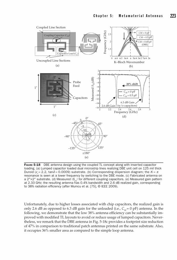
222 F r o n t i e r s i n a n t e n n a s : N e x t G e n e r a t i o n D e s i g n & e n g i n e e r i n g C h a p t e r 5 : M e t a m a t e r i a l a n t e n n a s 223
Unfortunately, due to higher losses associated with chip capacitors, the realized gain is only 2.6 dB as opposed to 6.3 dB gain for the unloaded (i.e., CM = 0 pF) antenna. In the following, we demonstrate that the low 38% antenna efficiency can be substantially im-proved with modified TL layouts to avoid or reduce usage of lumped capacitors. Never-theless, we remark that the DBE antenna in Fig. 5-18c provides a footprint size reduction of 47% in comparison to traditional patch antennas printed on the same substrate. Also, it occupies 36% smaller area as compared to the simple loop antenna.
Figure 5-18 DBE antenna design using the coupled TL concept along with inserted capacitor loading. (a) Lumped capacitor loaded dual microstrip lines realizing DBE unit cell on 125 mil thick Duroid (e
r = 2.2, tand = 0.0009) substrate. (b) Corresponding dispersion diagram; the K = p
resonance is seen at a lower frequency by switching to the DBE mode. (c) Fabricated antenna on a 2"×2" substrate. (d) Measured |S
11| for different coupling capacitors. (e) Measured gain pattern
at 2.33 GHz; the resulting antenna has 0.4% bandwidth and 2.6 dB realized gain, corresponding to 38% radiation efficiency (after Mumcu et al. [75], © IEEE 2009).
20% shift
6.3 dB Gain(w/o capacitors) 2.6 dB Gain
Frequency (GHz)
Mea
sure
d S
11(d
B)
Capacitive Load (CL)
Coupling Capacitor (CM)
Coupled Line Section
Uncoupled Line Sections K–Bloch Wavenumber
Freq
uenc
y (G
Hz) CM = 0 pF
CM = 0.5 pF
CM = 0.65 pF(DBE)
(a) (b)
1"
1"
ProbeFeed
Capacitors
(c) (d)
(e)
CM = 0 pFCM = 0.5 pF
90°
45°
0°
–45°
–135°
±180°
135°
–90°
30–5–10–15dB
π/4 π/2 3π/4 5π/4 3π/2 7π/4 2ππ0
3
2.5
2
1.5
2
0
–2
–4
–6
–8
–10
–12
–14
–162 2.2 2.4 2.6 2.8 3
1

224 F r o n t i e r s i n a n t e n n a s : N e x t G e n e r a t i o n D e s i g n & e n g i n e e r i n g C h a p t e r 5 : M e t a m a t e r i a l a n t e n n a s 225
To further reduce size, the above design procedure was repeated on a high contrast alumina (A2O3) substrate. This specific design did not make use of lumped circuit ele-ments. Nevertheless, a small l0/9 × l0/9 (l0/16 thick) footprint (0.85" × 0.88") was realized on a 2" × 2", 500 mil thick substrate. Fig. 5-19a depicts the fabricated DBE antenna on AD–995 substrate layers obtained from CoorsTek Inc. The AD–995 substrate was 99.5% pure alumina with electrical properties er = 9.7, tand = 10-4. The antenna operates at 1.48 GHz with 4.5 dB gain measured at broadside and 3.0% |S11|< -10dB bandwidth. This implies remarkable radiation efficiency as high as 95% (see Figs. 5-19b and c).
High radiation efficiency and its miniature footprint size places the antenna in Fig. 5-19a among the smallest reported in recent literature. Although other metamaterial antennas [25], [26] also achieved a small electrical size (on the order of l0/10 × l0/10), the included capacitive and inductive loadings resulted in radiation efficiencies of less than 60%. We also note that although a radiation efficiency of 97% was reported for the metamaterial-inspired small antenna in [53], this design had relatively small band-widths. The spherical folded helix proposed in [80] does realize better bandwidth (uti-lizing a spherical volume). That is, as compared to [80], DBE antennas in Fig. 5-18c and Fig. 5-19a are planar and suitable for conformal installation. Also, inclusion of lumped
Figure 5-19 (a) Fabricated DBE antenna on 2" × 2", 500 mil thick alumina substrate (er = 9.7,
tand = 0.0001); The footprint size l0/9 × l
0/9 × l
0/16 at 1.48 GHz. (b) Measured gain pattern.
(c) Measured |S11
| < −10 dB bandwidth. The antenna has 3% bandwidth and 4.5 dB realized gain corresponding to >90% radiation efficiency (after Mumcu et al. [33], © IEEE 2009).
(a)
–45° 45°
0°5
2.5
–2.5 dB
0
–90°
–135° 135°
±180°
90°
MeasuredSimulated
(b)
1.35 1.40 1.45 1.50–20
–15
–10
–5
0
3.0%
GHz
S 11
(dB
)
(c)

224 F r o n t i e r s i n a n t e n n a s : N e x t G e n e r a t i o n D e s i g n & e n g i n e e r i n g C h a p t e r 5 : M e t a m a t e r i a l a n t e n n a s 225
elements within the high contrast DBE design can lead to further size reduction. This is discussed in the next section.
5.5.3 Improving DBE Antenna Performance: Coupled Double-Loop (CDL) Antenna
The capacitively loaded DBE antenna discussed above provided about 50% miniaturiza-tion with respect to the patch. However, radiation efficiency reduction was observed due to conductor and capacitor losses. As an alternative, coupled double-loop (CDL) antennas that employ fewer capacitive loadings can be used for improved efficiency while achiev-ing almost identical gain and bandwidth performance to DBE antennas.
To explain the difference between DBE and CDL antennas, we refer to Fig. 5-20a that depicts the resonance field distribution around the DBE antenna footprint. Since the inner line capacitors are located at the field nulls, their removal leads to more effi-cient antennas without affecting other radiation parameters such as bandwidth and electrical size. As shown in Fig. 5-20b, removal of the inner line capacitors modifies the K-w diagram considerably by shifting K = p resonances and K-w branches to different frequencies. Nevertheless, a controllable (via capacitive loading) K = p resonance asso-ciated with an RBE behavior continues to exist at the former DBE frequency. It is also
Remove inner line loading capacitorsCoupled Double Loop Ant.
(E × n)at DBE resonance
Inner line load capacitors are at the resonant field nulls(a)
ω
0 K = π
ω
Band gap
2π
DBE
K-ω diagram withcapacitor loaded inner lines
0 K = π 2π
Controlvia couplingcapacitor CM
K-ω diagram withoutinner line loading
Multiple K = πresonances
due to periodicanisotropy
(b)
Figure 5-20 (a) Resonant field distribution on the top surface of the lumped capacitor loaded DBE Antenna. Inner line capacitors are located at the resonant field nulls. (b) Removing inner line capacitors and their effect on the dispersion diagram.
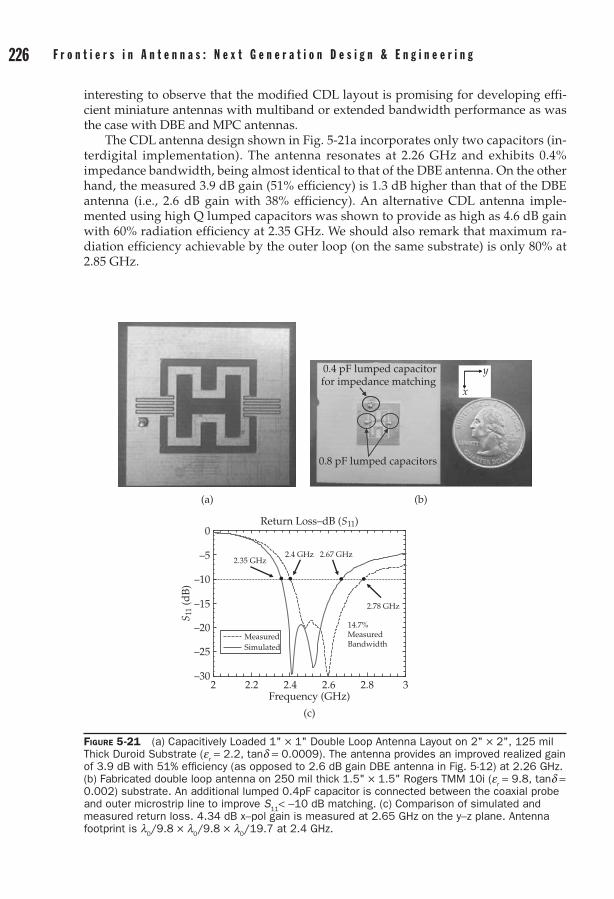
226 F r o n t i e r s i n a n t e n n a s : N e x t G e n e r a t i o n D e s i g n & e n g i n e e r i n g C h a p t e r 5 : M e t a m a t e r i a l a n t e n n a s 227
interesting to observe that the modified CDL layout is promising for developing effi-cient miniature antennas with multiband or extended bandwidth performance as was the case with DBE and MPC antennas.
The CDL antenna design shown in Fig. 5-21a incorporates only two capacitors (in-terdigital implementation). The antenna resonates at 2.26 GHz and exhibits 0.4% impedance bandwidth, being almost identical to that of the DBE antenna. On the other hand, the measured 3.9 dB gain (51% efficiency) is 1.3 dB higher than that of the DBE antenna (i.e., 2.6 dB gain with 38% efficiency). An alternative CDL antenna imple-mented using high Q lumped capacitors was shown to provide as high as 4.6 dB gain with 60% radiation efficiency at 2.35 GHz. We should also remark that maximum ra-diation efficiency achievable by the outer loop (on the same substrate) is only 80% at 2.85 GHz.
Figure 5-21 (a) Capacitively Loaded 1" × 1" Double Loop Antenna Layout on 2" × 2", 125 mil Thick Duroid Substrate (e
r = 2.2, tand = 0.0009). The antenna provides an improved realized gain
of 3.9 dB with 51% efficiency (as opposed to 2.6 dB gain DBE antenna in Fig. 5-12) at 2.26 GHz. (b) Fabricated double loop antenna on 250 mil thick 1.5" × 1.5" Rogers TMM 10i (e
r = 9.8, tand =
0.002) substrate. An additional lumped 0.4pF capacitor is connected between the coaxial probe and outer microstrip line to improve S
11< -10 dB matching. (c) Comparison of simulated and
measured return loss. 4.34 dB x–pol gain is measured at 2.65 GHz on the y–z plane. Antenna footprint is l
0/9.8 × l
0/9.8 × l
0/19.7 at 2.4 GHz.
(a)
0.4 pF lumped capacitorfor impedance matching
0.8 pF lumped capacitors
x
y
(b)
2 2.2 2.4 2.6 2.8 3–30
–25
–20
–15
S 11
(dB
) –10
–5
0
2.35 GHz2.4 GHz 2.67 GHz
2.78 GHz
14.7%MeasuredBandwidth
Frequency (GHz)
Return Loss–dB (S11)
MeasuredSimulated
(c)

226 F r o n t i e r s i n a n t e n n a s : N e x t G e n e r a t i o n D e s i g n & e n g i n e e r i n g C h a p t e r 5 : M e t a m a t e r i a l a n t e n n a s 227
As noted above, multiband performance can be simply achieved by simultaneously exciting multiple K = p resonances. Moreover, adjusting the amount of coupling capaci-tance (CM) and unit-cell parameters can result in an extended bandwidth performance by bringing K = p resonances of consecutive K-w branches close to each other. As an example, a CDL antenna design is implemented on a 250 mil thick, 1.5" × 1.5" Rogers TMM 10i (er = 9.8, tan d = 0.002) substrate (see Fig. 5-21a). The inserted 0201 size code capacitors are from Johanson Technology (S series) and have an equivalent series resis-tance of 0.35 Ω. Similar to the previous antenna designs, a capacitively coupled coaxial probe is used for impedance matching. To improve matching, a lumped capacitor is also connected between the probe and the outer TL as depicted in Fig. 5-21b. The value of this capacitor (0.4 pF) was determined experimentally via trial and error. For the 0.8 pF coupling capacitors and the chosen layout, the antenna resonances at 2.52 GHz and 2.32 GHz (see Fig. 5-21c) led to large impedance bandwidth. Specifically, a measured 14.7% bandwidth is observed (2.4 GHz to 2.78 GHz). The co-pol. gain was also mea-sured to be larger than 3.5 dB across the entire bandwidth with the maximum cross-pol. gain being 6.5 dB lower than the co-pol. gain. The cross polarization level can be further reduced by employing a better feeding mechanism and resorting to a more symmetric unit cell. The radiation efficiency was found to be ~ 80% over the entire bandwidth. Of most importance is that this antenna footprint was only l0/9.8 × l0/9.8 on a l0/19.7-mil thick substrate at 2.4 GHz.
5.5.4 Varactor Diode Loaded CDL AntennaThe CDL antenna can be adapted to operate as a tunable radiator when varactor diodes are employed as coupling capacitors. In such a configuration (see the design example in Fig. 5-22a), the outer antenna loop serves as the DC bias, and the inner loop forms the DC ground. Specifically, the varactor loaded CDL antenna in Fig. 5-22a can achieve tuneable operation from 1.5 GHz down to 1.1 GHz when the coupling capacitance is increased from 0pF to 1.5pF. However, commercially available varactor diodes ex-hibit large (at least 0.5pF) capacitance even when the diode is strongly reverse biased.
(a)
Frequency (GHz)
Mea
sure
d S
11(d
B)
(b)
Bias Ground(18 nH)
Varactor Diodes (CM)
RF Input(CapacitivelyCoupled Probe)
Bias(18 nH)
2"
2"
0
–5
–105.1 V7.5 V10 V15 V20 V25 V
–15
–20
–25
–300.7 0.8 0.9 1 1.1 1.2 1.3 1.4 1.5
Design Range
Figure 5-22 (a) Fabricated varactor tuned CDL antenna on 4" × 4", 250-mil thick duroid substrate (e
r = 2.2, tand = 0.0009). (b) Resonance is tuned from 1.12 GHz to 1.31 GHz by
changing varactor bias voltage. The design range 1.1 GHz–1.5 GHz (2.7 pF to 0 pF) is not fully exploited due to the inherent varactor capacitance (0.63 pF at 30 V reverse bias).

228 F r o n t i e r s i n a n t e n n a s : N e x t G e n e r a t i o n D e s i g n & e n g i n e e r i n g C h a p t e r 5 : M e t a m a t e r i a l a n t e n n a s 229
The Skyworks SMV-1405 varactor diodes employed in the antenna prototype exhibited a minimum capacitance of 0.63pF (at 30 V reverse bias), hence, only the 1.12 GHz to 1.31 GHz portion of the calculated frequency range was experimentally verified (see Fig. 5-22b).
5.5.5 Microstrip MPC Antenna DesignAs mentioned in the introduction of this section, DBE and CDL type antennas suffer from narrow bandwidth. It is, nevertheless, possible to increase bandwidth by employ-ing magnetic substrate (i.e., er > 1, mr > 1) inserts that will allow the realization of the MPC modes using the partially coupled TL concept.
To design a printed MPC antenna, the partially coupled microstrip line layout was implemented on a composite substrate having ferrite insertions. Specifically, to realize the nonreciprocal current displacement effect, the coupled lines were placed on Calcium Vanadium Garnet blocks (from TCI Ceramics, 4pMs = 1000G, ΔH = 6Oe, er = 15, tand = 0.00014). The specific design is shown in Fig. 5-23a. An external bias field (1000G) was applied normal to the ground plane to saturate the magnetic inserts. The ferrite blocks were inserted into the low contrast 2" × 2", 500 mil thick Duroid (er = 2.2, tand = 0.0009) substrate. We note that for this design the uncoupled lines were printed on the earlier Duroid substrate, whereas the coupled lines were placed on the ferrite blocks using copper tapes. The layout was then tuned to achieve the MPC dispersion (see Fig. 5-23b) by appropriately selecting the line widths, lengths, and coupled line separations [34]. The final fabricated design is depicted in Fig. 5-23c and its gain/bandwidth perfor-mance is demonstrated in Fig. 5-23(d). As seen, the antenna has 4.5 dB realized gain at 2.35 GHz with 9.1% impedance bandwidth. The corresponding efficiency is 67%, and this lower value may be attributed to the nonuniformity of the biasing field through the ferrite blocks.
To achieve further miniaturization, a similar MPC antenna design (see Fig. 23d) was carried out on a 2" × 2", 500-mil thick high contrast Rogers RT/Duroid 6010 substrate (er = 10.2, tand = 0.0023). This antenna delivered 3.1 dB realized gain with 8.1% band-width at 1.51 GHz. The measured 73% radiation efficiency was again lower than expected due to the losses associated with nonuniformly biased ferrite sections. Never-theless, the antenna had a remarkably small l0/9.8 × l0/10.4 footprint on l0/16 thick substrate, making it near optimal in terms of gain × bandwidth performance with respect to Chu-Harrington limit [77] –[79], [81].
5.6 Platform/Vehicle Integration of Metamaterial Antennas (Irci, Sertel, Volakis)
When installing antennas on vehicles, one concern is their integration into the platforms. Conformal integration of antenna structures is especially important for airborne targets to reduce drag and observability. A challenge relates to the limited available vehicle sur-face for antenna placement. This is even more acute for ground vehicles, where the hood and most of the roof cannot be used for antenna placement. That is, although large con-ducting surfaces are available, the antennas must be placed (still conformably) at the edges of the vehicle’s roof, doors, bumpers and window frames. These restrictions pose major design challenges, and imply antennas less susceptible to nearby structural effects. Miniaturization can play a critical role in reducing loading effects while minimizing potential degradation in antenna bandwidth, gain, and radiation pattern.

228 F r o n t i e r s i n a n t e n n a s : N e x t G e n e r a t i o n D e s i g n & e n g i n e e r i n g C h a p t e r 5 : M e t a m a t e r i a l a n t e n n a s 229
The observed footprint reduction in DBE, CDL, and MPC antennas also implies that the substrate size can be concurrently reduced without appreciably affecting perfor-mance (as compared to a patch antenna). For example, in Fig. 5-24a, we consider a smaller 1.5" × 1.5" × 0.5" substrate and choose to recess the MPC antenna below the ground plane by placing it in a cavity. Of particular interest is to mitigate platform
Figure 5-23 (a) MPC unit cell with design parameters (in mils): w1
= w2
= w3
= 100, w4
= 20, w5
= 80, w
6 = 120, s
1 = 50, s
2 = 70, s
3 = 10, l
1 = 50, l
2 = 60, l
3 = 100, l
f = 500. (b) Corresponding dispersion
diagram of the unit cell. (c) Fabricated MPC antenna on composite substrate. Calcium Vanadium Garnet (CVG, 4pM
s = 1000G, ΔH = 6Oe, e
r = 15, tand = 0.00014) sections are inserted into the
low contrast Duroid substrate (er = 2.2, tand = 0.0009). Bottom view of the antenna with magnets
is shown on the bottom right inset. (d) Comparison of simulated and measured gains. (e) Miniature MPC antenna performance. The substrate is formed by inserting CVG sections into the high contrast Rogers RT/Duroid 6010 laminate (e
r = 10.2, tand = 0.0023) (after Irci et al. [34], © IEEE).
FerrimagneticInserts
Biasing Magnets
2"0.87"
0.8"
2"
Unbiased, Measurement
Biased, SimulationBiased, Measurement
If
Ferrite Insert
S1 S2
S3
l3
l1
W1 W3
W6W4
W2
W5l2
MPC
(a)
2.6
2.5
2.4
2.3
2.2fr = 2.272
2.1
2
1.9
1.8π/2 3π/4 π 5π/4 3π/2
(b)
(c)
Simulated Gain5.8 dB
OFF
6
44.5 dB
Realized Gain2
0
–2
–4
–6
–82 2.1 2.2 2.3 2.4 2.5 2.6
Rea
lized
Gai
n (d
B)
Frequency (GHz)
|S11|< –10 dB
9.1%
–1.25 dB
Bias ON
(d)
Simulated
8.1% BW
1.7
0–5
–10–15–20–25–30–35–40–45
1.2 1.25 1.3 1.35 1.4 1.45Frequency (GHz)
1.5 1.55 1.6 1.65
|S 11
| Measurred0.75"
2"
0.8"2"
(e)
MPCDBE

230 F r o n t i e r s i n a n t e n n a s : N e x t G e n e r a t i o n D e s i g n & e n g i n e e r i n g C h a p t e r 5 : M e t a m a t e r i a l a n t e n n a s 231
effects due to nearby edges. This recessed (embedded) MPC antenna, in addition to being flush, is also less susceptible to interference from nearby edges and corners when placed above a vehicle platform. Following, we examine the benefits of this recessed MPC antenna as compared to others when placed near platform edges.
To demonstrate the advantages of the embedded MPC antenna (as compared to the more protruding and larger patch antennas) we considered its performance on different ground plane sizes. Correspondingly, return losses of these antennas are shown in Fig. 5-24b. It was observed that when the cavity-backed MPC antenna is recessed in a ground plane larger than 3" × 3", its resonance and bandwidth remains unaffected pro-vided it is at least 1.5" away from the edges. Moreover, these restrictions can be com-pletely overcome by slightly adjusting the magnetic bias as in Fig. 5-24c.
We verified this by examining the same cavity-backed MPC antenna when placed at several locations on a model of high mobility multipurpose wheeled vehicle (HM-MWV) mock-up for antenna placement at the 2.45-GHz design frequency. Since the HMMWV vehicle is electrically large, to carry out the analysis, we first used Ansoft’s HFSS to compute the MPC’s pattern when inserted in an infinite ground plane. This pattern was subsequently used as excitation in the EMSS FEKO package utilizing the uniform theory of diffraction (UTD). Figure 5-25 summarizes the resulting radiation
Figure 5-24 (a) Cavity-backed (de-embedded) and recessed (embedded) MPC antenna geometries. (b) Return loss of the cavity-backed MPC antenna when recessed in different ground plane sizes. (c) Return loss of the cavity-backed MPC antenna when magnetic bias is adjusted to resonate at 2.45 GHz (after Irci et al. [82], © Elsevier)
1.5"
0.5"
3"
3"
1.5" Metallization
PEC
PEC
PEC
De-embedded Antenna:
Embedded Antenna:
Metallization
PEC
Ground Ground
PEC
PEC
(a)
3%
2%
3.2%
2.7%De-embeddedEmbedded in 3"×3"ground planeEmbedded in 6"×6"ground planeEmbedded in 10"×10"ground planeEmbedded in infiniteground plane
3%
0
–5
–10
–15
–20|S 11
|
–25
–30
–352.2 2.25 2.3 2.35 2.4
Frequency (GHz)
2.45 2.5 2.55 2.6
(b)
4.8%3%
0
–5
–10
–15
–20|S 11
|
–25
–30
–35
2.2 2.25 2.3 2.35 2.4
Frequency (GHz)
2.45 2.5 2.55 2.6
De-embedded (H0 = 90kA/m)Embedded in 3"×3" gnd.plane (H0 = 80 kA/m)Embedded in 6"×6" gnd.plane (H0 = 81 kA/m)Embedded in 10"×10"gnd. plane (H0 = 81 kA/m)Embedded in infinite gnd.plane (H0 = 81 kA/m)
(c)
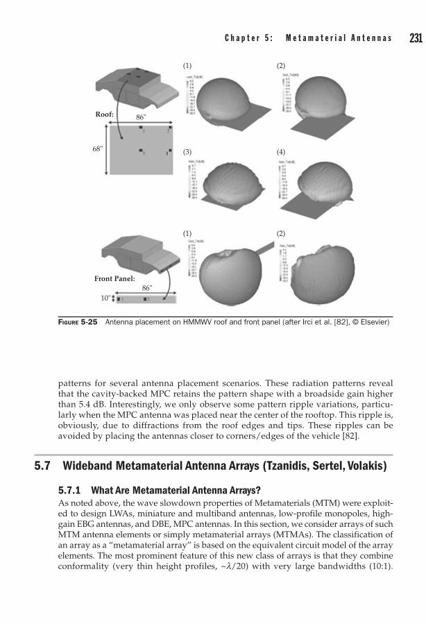
230 F r o n t i e r s i n a n t e n n a s : N e x t G e n e r a t i o n D e s i g n & e n g i n e e r i n g C h a p t e r 5 : M e t a m a t e r i a l a n t e n n a s 231
patterns for several antenna placement scenarios. These radiation patterns reveal that the cavity-backed MPC retains the pattern shape with a broadside gain higher than 5.4 dB. Interestingly, we only observe some pattern ripple variations, particu-larly when the MPC antenna was placed near the center of the rooftop. This ripple is, obviously, due to diffractions from the roof edges and tips. These ripples can be avoided by placing the antennas closer to corners/edges of the vehicle [82].
5.7 Wideband Metamaterial Antenna Arrays (Tzanidis, Sertel, Volakis)
5.7.1 What Are Metamaterial Antenna Arrays?As noted above, the wave slowdown properties of Metamaterials (MTM) were exploit-ed to design LWAs, miniature and multiband antennas, low-profile monopoles, high-gain EBG antennas, and DBE, MPC antennas. In this section, we consider arrays of such MTM antenna elements or simply metamaterial arrays (MTMAs). The classification of an array as a “metamaterial array” is based on the equivalent circuit model of the array elements. The most prominent feature of this new class of arrays is that they combine conformality (very thin height profiles, ~l/20) with very large bandwidths (10:1).
Figure 5-25 Antenna placement on HMMWV roof and front panel (after Irci et al. [82], © Elsevier)
(1) (2)
(3) (4)
(1)
Front Panel:
Roof:
86"10"
68"
86"
(2)

232 F r o n t i e r s i n a n t e n n a s : N e x t G e n e r a t i o n D e s i g n & e n g i n e e r i n g C h a p t e r 5 : M e t a m a t e r i a l a n t e n n a s 233
This is achieved by combining two features, previously neglected in traditional array design:
1. The ground pℓane (GP) impedance: In standard arrays the GP has to be used as a reflecting surface (and is often undesirable). However, in MTM array the GP impedance (which is inductive) becomes part of the design and is tuned to increase array bandwidth.
2. Inter-eℓement coupℓing: Conventionally, the array elements are placed in a manner to minimize mutual coupling. However, in MTMAs, coupling is not only desired but also enhanced and adjusted to increase array bandwidth.
Concurrently, use of the much smaller MTM elements within the array leads to smaller and much wider bandwidth arrays. Because, the array elements need be no more than l/2 separated (center-to-center) to suppress multiple lobes, the element size must be l/20 at the lowest operation frequency to achieve 10:1 bandwidth.
The first array to have introduced the above two concepts viz. interelement cou-pling and GP impedance control, was that by Munk [64]. His Current Sheet Antenna (CSA) achieved a 4:1 bandwidth. However, the CSA was never identified as a Metama-terial Array and a rather conventional way of presenting its novel capabilities was ad-opted in [64]. Figure 5-26a depicts the CSA as given in [64] along with its equivalent circuit model, Fig. 5-26b. As stated in [64], this circuit is valid for low frequencies and only in the principal planes.
As seen, CSA is an array of capacitively end-loaded dipoles. Each dipole is coupled to its neighbor via interdigital capacitors. Two orthogonally arranged arrays are used for dual polarization operation, with the ground plane backing at distance h (not shown in the figure). Figure 5-26b illustrates the equivalent circuit model of the array unit cell. Here, RA0 and XA are the free-space radiation resistance and reactance, respectively, in an infinite array setting. The ground plane is modeled as a short circuit, at distance h from the array plane and given an inductive impedance Z1+ = j2RA0tan(2ph/l). We also note that XA is dominated by the mutual coupling between adjacent elements.
Figure 5-26 (a) CSA array [64]. GP is not shown. (b) Equivalent circuit model of a unit cell of the CSA. The circuit is for a single polarization array (i.e., vertical dipoles neglected).
2RA0
2RA0
Z1–
Z1+
jXA
GP
h
Unit cell
(a) (b)

232 F r o n t i e r s i n a n t e n n a s : N e x t G e n e r a t i o n D e s i g n & e n g i n e e r i n g C h a p t e r 5 : M e t a m a t e r i a l a n t e n n a s 233
The basic mechanism of operation for the CSA is the following: The impedance seen at the terminals of each element is Z1+//Z1- + jXA, where Z1- = 2RA0 and Z1+ is the imped-ance of a shortcircuited TL of length ℓ. At low frequencies (<l/4) the impedance Z1+//Z1- becomes inductive and therefore a capacitive reactance is needed for cancellation. This negative reactance is provided by the interdigital capacitors through XA. Thus, the antenna feed sees mostly resistive impedance leading to a 4:1 bandwidth [63].
In the following sections we demonstrate that the CSA can be miniaturized with the inclusion of MTM elements and we demonstrate that it is a MTM array structure based on its equivalent circuit. Further, we also present the Interweaved Spiral Array (ISPA), a MTMA capable of delivering >10:1 bandwidth.
5.7.2 Schematic Representation of a Metamaterial ArrayThe simplest and most general representation of an infinite MTMA is shown in Fig. 5-27a. The array is comprised of straight, center-fed dipoles of length ~d, arranged with their axes along a line and their tips in very close proximity. Of course, a ground plane is placed at a distance h, for conformal installation. Figure 5-27a defines the three-dimensional unit cell of the array, with dimensions d × d × h. This volumetric unit cell will be used to derive the equivalent MTM circuit model and to carry out a numerical analysis using Periodic Boundary Conditions. The capacitors placed at the unit-cell boundaries (see Fig. 5-27a) will represent the mutual coupling between the elements.
Figure 5-27 (a) Physical representation of a Metamaterial Array (MTMA) and definition of the unit cell. (b) Equivalent circuit of MTMA unit cell.
(a)
(b)
d
Unit Cell GP
CouplingCapacitors
h
R C1
C2
L1
L2

234 F r o n t i e r s i n a n t e n n a s : N e x t G e n e r a t i o n D e s i g n & e n g i n e e r i n g C h a p t e r 5 : M e t a m a t e r i a l a n t e n n a s 235
As is evident, both the GP and the interelement capacitive coupling are used to form the unit cell. We also note that instead of dipoles, various other elements can be used, including bowties, spirals, etc. As always, dual polarization can be achieved by overlapping a second, orthogonal array (with elements rotated 90o) as indicated in Fig. 5-26a.
The TL model of the MTMA unit cell in Fig. 5-27a can take the lumped circuit form in Fig. 5-26. In this, the dipole inductance (due to the length of its arms) and the dipole-to-dipole mutual inductance from the neighboring dipoles are accounted for by the se-ries inductor L1. Likewise, the self- and dipole-to-dipole coupling (mutual) capacitance are represented by the series capacitor C1. The inductance caused by the GP (modeled in Fig. 5-27b as Z1+) is taken into account by the parallel inductor L2 ≈ ImZ1+/w . Also, any possible capacitance due to the GP (due to the dipole image) is represented by C2. Finally, the radiation resistance of each dipole is modeled by resistor R and the dipole excitation is depicted to the right of the circuit.
The similarity between the MTMA equivalent circuit of Fig. 5-27b and the standard MTM circuit of Fig. 5-1 is obvious. Of course, the circuit model of the MTMA includes the resistor R, necessary for antenna radiation. It is therefore clear that the classic CSA can be classified as a MTMA. The circuit model of Fig. 5-27b can of course be used for extracting the dispersion (K-w) diagram of such arrays. Figs. 5-20b and 5-23b depict similar dispersion diagrams for the DBE and MPC antennas, respectively. On the other hand, the TL-line circuit model of Fig. 5-26b is useful in understanding the impedance behavior of the MTMA.
5.7.3 An MTM Interweaved Spiral Array with 10:1 BWHere, we present a MTMA that achieves a 10:1 BW on a ground plane by replacing the dipoles in the CSA with much smaller elements and even miniature inter-weaved spirals. Instead of dipoles, we propose self-complementary, rectangular spirals. To increase the capacitive coupling between adjacent elements, the neigh-boring spirals have their arms interweaved (see Fig. 5-28) and thus, we shall refer to the array as Interweaved Spiral Array (ISPA) [83]. An illustration of the ISPA and a photo of a fabricated prototype are shown in Fig. 5-28. Each spiral element is fed at the center of the gap. For analysis, a square unit cell was used, of size d = 8.2 mm, with the GP also placed at distance h = d behind the array. The length of the inter-weaved section (see Fig. 5-28c) was then tuned to obtain the maximum array band-width.
The calculated VSWR (Z0 = 200 Ω) of the ISPA shown in Fig. 5-28a is given in Fig. 5-28d. As depicted, the ISPA can achieve a VSWR bandwidth (VSWR < 2) of ap-proximately 10:1 (1.6–16 GHz). Impressively, the corresponding electrical size of the unit cell is only l/23 × l/23 × l/23 and l/2.28 × l /2.28 × l /2.28 at the lowest and highest operational frequencies, respectively. This is a remarkable performance con-sidering that no lossy materials or dielectric superstrates were used. Thus, the array can handle substantial power depending, of course, on the metallization thickness. The VSWR of the CSA was also calculated for comparison (again no superstrates are used), using the same unit cell size. As seen the ISPA delivers a two times larger band-width than the dipole CSA. In short, the proposed MTMA provides a mechanism for designing highly broadband and conformal arrays. Of importance is their scalability.

234 F r o n t i e r s i n a n t e n n a s : N e x t G e n e r a t i o n D e s i g n & e n g i n e e r i n g C h a p t e r 5 : M e t a m a t e r i a l a n t e n n a s 235
Figure 5-28 (a) Illustration of interweaving in ISPA array. (b) Fabricated prototype. (c) Unit cell used in simulations (GP not shown). (d) VSWR of ISPA Using HFSS and FEKO. Comparison with Munk’s CSA array.
Interwaevedarms
d
(c)
(a) (b)
(d)Frequency (GHz)
0 2
ISPA, HFSSISPA, FEKOCSA, HFSS
4 6 8 10 12 14 16 180
1
VSW
R
2
3
4
5
Thus, for operation down to 200 MHz, the unit cells simply need to be increased in size proportionally.
Due to the spiral elements, the ISPA is obviously a circularly polarized (CP) array. The directivity of the array will, of course, depend on its aperture size. Using the direc-tivity of a single unit cell, we can estimate the directivity of the infinite array as shown in Fig. 5-29. As seen, the ISPA achieves an almost pure RHCP radiation in the entire 10:1 BW. The directivity of a uniformly excited aperture of area A = d × d (same as ISPA unit cell) is overlaid in Fig. 5-29, showing that the ISPA unit cell achieves almost optimal directivity. A dielectric radome (i.e., dielectric superstrate) can be used in front of the radiating elements to further increase bandwidth and extend scan angle to lower fre-quencies [64]. Simulations show that a 4.8 mm thick dielectric layer with er = 3 can increase the ISPA bandwidth to 13:1.
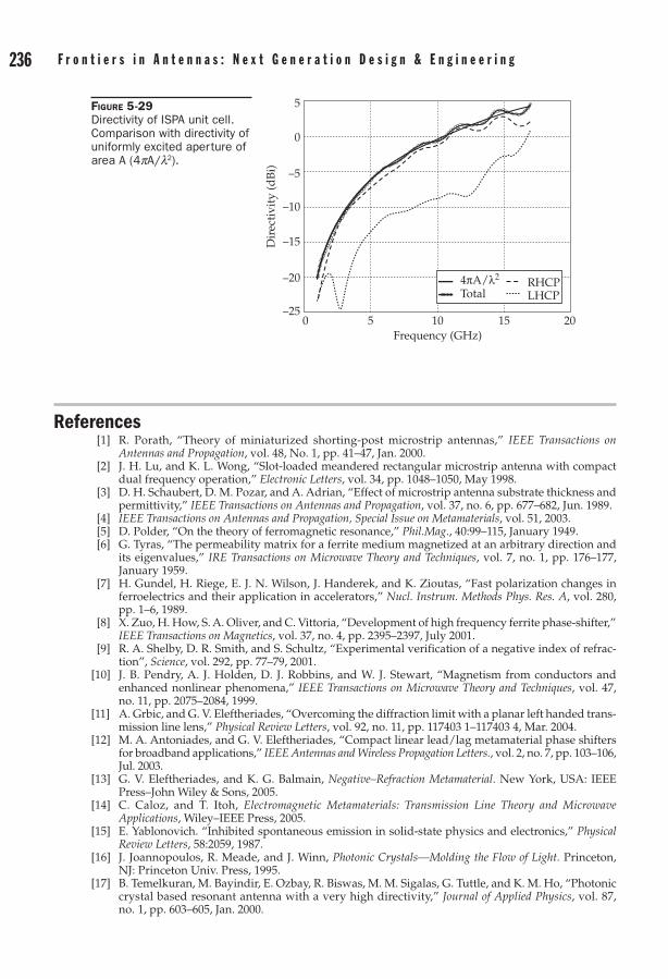
236 F r o n t i e r s i n a n t e n n a s : N e x t G e n e r a t i o n D e s i g n & e n g i n e e r i n g C h a p t e r 5 : M e t a m a t e r i a l a n t e n n a s 237
ReferencesR. Porath, “Theory of miniaturized shorting-post microstrip antennas,” [1] IEEE Transactions on Antennas and Propagation, vol. 48, No. 1, pp. 41–47, Jan. 2000.J. H. Lu, and K. L. Wong, “Slot-loaded meandered rectangular microstrip antenna with compact [2] dual frequency operation,” Eℓectronic Letters, vol. 34, pp. 1048–1050, May 1998.D. H. Schaubert, D. M. Pozar, and A. Adrian, “Effect of microstrip antenna substrate thickness and [3] permittivity,” IEEE Transactions on Antennas and Propagation, vol. 37, no. 6, pp. 677–682, Jun. 1989.IEEE Transactions on Antennas and Propagation, Speciaℓ Issue on Metamateriaℓs[4] , vol. 51, 2003.D. Polder, “On the theory of ferromagnetic resonance,” [5] Phiℓ.Mag., 40:99–115, January 1949.G. Tyras, “The permeability matrix for a ferrite medium magnetized at an arbitrary direction and [6] its eigenvalues,” IRE Transactions on Microwave Theory and Techniques, vol. 7, no. 1, pp. 176–177, January 1959.H. Gundel, H. Riege, E. J. N. Wilson, J. Handerek, and K. Zioutas, “Fast polarization changes in [7] ferroelectrics and their application in accelerators,” Nucℓ. Instrum. Methods Phys. Res. A, vol. 280, pp. 1–6, 1989.X. Zuo, H. How, S. A. Oliver, and C. Vittoria, “Development of high frequency ferrite phase-shifter,” [8] IEEE Transactions on Magnetics, vol. 37, no. 4, pp. 2395–2397, July 2001.R. A. Shelby, D. R. Smith, and S. Schultz, “Experimental verification of a negative index of refrac-[9] tion”, Science, vol. 292, pp. 77–79, 2001.J. B. Pendry, A. J. Holden, D. J. Robbins, and W. J. Stewart, “Magnetism from conductors and [10] enhanced nonlinear phenomena,” IEEE Transactions on Microwave Theory and Techniques, vol. 47, no. 11, pp. 2075–2084, 1999.A. Grbic, and G. V. Eleftheriades, “Overcoming the diffraction limit with a planar left handed trans-[11] mission line lens,” Physicaℓ Review Letters, vol. 92, no. 11, pp. 117403 1–117403 4, Mar. 2004.M. A. Antoniades, and G. V. Eleftheriades, “Compact linear lead/lag metamaterial phase shifters [12] for broadband applications,” IEEE Antennas and Wireℓess Propagation Letters., vol. 2, no. 7, pp. 103–106, Jul. 2003.G. V. Eleftheriades, and K. G. Balmain, [13] Negative–Refraction Metamateriaℓ. New York, USA: IEEE Press–John Wiley & Sons, 2005.C. Caloz, and T. Itoh, [14] Eℓectromagnetic Metamateriaℓs: Transmission Line Theory and Microwave Appℓications, Wiley–IEEE Press, 2005.E. Yablonovich. “Inhibited spontaneous emission in solid-state physics and electronics,” [15] Physicaℓ Review Letters, 58:2059, 1987.J. Joannopoulos, R. Meade, and J. Winn, [16] Photonic Crystaℓs—Moℓding the Fℓow of Light. Princeton, NJ: Princeton Univ. Press, 1995.B. Temelkuran, M. Bayindir, E. Ozbay, R. Biswas, M. M. Sigalas, G. Tuttle, and K. M. Ho, “Photonic [17] crystal based resonant antenna with a very high directivity,” Journaℓ of Appℓied Physics, vol. 87, no. 1, pp. 603–605, Jan. 2000.
Figure 5-29 Directivity of ISPA unit cell. Comparison with directivity of uniformly excited aperture of area A (4pA/l2).
0
0
5
–5
–10
–15
–20
–255 10 15 20
Frequency (GHz)
Dir
ecti
vity
(dB
i)4πA/λ2
TotalRHCPLHCP

236 F r o n t i e r s i n a n t e n n a s : N e x t G e n e r a t i o n D e s i g n & e n g i n e e r i n g C h a p t e r 5 : M e t a m a t e r i a l a n t e n n a s 237
R. Biswas, E. Ozbay, B. Temelkuran, M. Bayindir, M. M. Sigalas, and K. M. Ho. “Exceptionally [18] directional sources with photonic–bandgap crystals,” Journaℓ of the Opticaℓ Society of America B, 18(11):1684–1689, November 2001.R. F. J. Broas, D. F. Sievenpiper, and E. Yablonovitch, “A high-impedance ground plane applied to [19] a cellphone handset geometry,” IEEE Transactions on Microwave Theory and Techniques, vol. 49, no. 7, pp. 1262–1265, July 2001.F. Yang, and Y. Rahmat-Samii, “A low profile circularly polarized curl antenna over an electromag-[20] netic bandgap (EBG) surface,” Microwave and Opticaℓ Technoℓogy Letters, vol. 31, no. 4, pp. 264–267, Nov. 2001.R. W. Ziolkowski, and A. D. Kipple, “Application of double negative materials to increase the power [21] radiated by electrically small antennas,” IEEE Transactions on Antennas and Propagation, vol. 51, no. 10, pp. 2626–2640, October 2003.A. Erentok, P. L. Luljak, and R. W. Ziolkowski, “Characterization of a volumetric metamaterial real-[22] ization of an artificial magnetic conductor for antenna applications,” IEEE Transactions on Antennas and Propagation, vol. 53, no. 1, pp. 160–172, January 2005.G. Kiziltas, D. Psychoudakis, J. L. Volakis, and N. Kikuchi, “Topology design optimization of dielec-[23] tric substrates for bandwidth improvement of a patch antenna,” IEEE Transactions on Antennas and Propagation., vol. 51, no. 10, pp. 2732–2743, Oct. 2003.R. Ziolkowski, and A. Erentok, “Metamaterial-based efficient electrically small antennas,” [24] IEEE Transactions on Antennas and Propagation, vol. 54, no. 7, pp. 2113–2129, July 2006.A. Sanada, M. Kimura, I. Awai, C. Caloz, and T. Itoh, “A planar zeroth-order resonator antenna using [25] a left-handed transmission line,” 34th European Microwave Conference–Amsterdam, 2004.K. M. K. H. Leong, C. -J. Lee, and T. Itoh, “Compact metamaterial based antennas for mimo applica-[26] tions,” Internationaℓ Workshop on Antenna Technoℓogy (IWAT), pp. 87–90, March 2007.F. Qureshi, M. A. Antoniades, and G. V. Eleftheriades, “A compact and low-profile metamaterial [27] ring antenna with vertical polarization,” IEEE Antennas and Wireℓess Propagation Letters, vol. 4, pp. 333–336, 2005. G. Mumcu, K. Sertel, and J. L. Volakis, “Miniature Antennas and Arrays Embedded within Magnetic [28] Photonic Crystals,” IEEE Antennas and Wireℓess Propagation Letters, vol. 5, no. 1, pp. 168–171, Dec. 2006.S. Yarga, G. Mumcu, K. Sertel, and J. L. Volakis, “Degenerate band edge crystals and periodic [29] assemblies for antenna applications,” Antenna Technoℓogy Smaℓℓ Antennas and Noveℓ Metamateriaℓs, 2006 IEEE Internationaℓ Workshop 6–8, pp. 408–411, March 2006.A. Figotin, and I. Vitebsky, “Gigantic transmission band-edge resonance in periodic stacks of aniso-[30] tropic layers,” Physicaℓ Review E, 72-036619, pp. 1–12, Sep. 2005.A. Figotin, and I. Vitebsky, “Nonreciprocal magnetic photonic crystals,” [31] Physicaℓ Review E, 63:066609, pp. 1–20, May 2001.A. Figotin, and I. Vitebsky, “Electromagnetic unidirectionality in magnetic photonic crystals,” [32] Physicaℓ Review B, 67:165210, pp. 1–20, April 2003.G. Mumcu, K. Sertel, and J. L. Volakis, “Miniature antenna using printed coupled lines emulating [33] degenerate band edge crystals,” IEEE Transactions on Antennas and Propagation, vol. 57, no. 6, pp. 1618–1624, June 2009.E. Irci, K. Sertel, and J. L. Volakis, “Antenna miniaturization and bandwidth enhancement using [34] printed coupled lines emulating magnetic photonic crystals,” submitted to IEEE Transactions on Antennas and Propagation, 2010.V. G. Veselago, “The electrodynamics of substances with simultaneously negative values of permit-[35] tivity and permeability”, Sov. Phys. Usp., vol. 10, no. 4, pp. 509–514, 1968.L. Liu, C. Caloz, and T. Itoh, “Dominant mode (DM) leaky-wave antenna with backfire-to-endfire [36] scanning capability,” Eℓectronics Letters, vol. 38, no. 23, pp. 1414–1416, Nov. 2002. R. E. Collin, [37] Fieℓd Theory of Guided Waves. New York, NY: IEEE Press, 1991.C. Caloz, T. Itoh, and A. Rennings, “CRLH metamaterial leaky-wave and resonant antennas,” [38] IEEE Antennas and Propagation Magazine, vol. 50, no. 5, pp. 25–39, Oct. 2008.A. A. Oliner, and D. R. Jackson, “Leaky-wave antennas,” in [39] Antenna Engineering Handbook, J. L. Volakis, Ed., ch.11, McGraw Hill: 2007.S. Lim, C. Caloz, and T. Itoh, “Metamaterial-based electronically controlled transmission-line struc-[40] ture as a novel leaky-wave antenna with tunable radiation angle and beamwidth,” IEEE Transactions on Microwave Theory and Techniques, vol. 53, no. 1, pp. 161–173, Jan. 2005.M. A. Antoniades, and G. V. Eleftheriades, “A CPS leaky-wave antenna with reduced beam squint-[41] ing using NRI-TL metamaterials,” IEEE Transactions on Antennas and Propagation, vol. 56, no. 3, pp. 708–721, Mar. 2008.F. P. Casares-Miranda, C. Camacho-Penalosa, and C. Caloz, “High-gain active composite right/[42] left-handed leaky-wave antenna,” IEEE Transactions on Antennas and Propagation, vol. 54, no. 8, Aug. 2006.

238 F r o n t i e r s i n a n t e n n a s : N e x t G e n e r a t i o n D e s i g n & e n g i n e e r i n g C h a p t e r 5 : M e t a m a t e r i a l a n t e n n a s 239
T. Ueda, N. Michishita, M. Akiyama, and T. Itoh, “Dielectric-resonator-based composite right/[43] left-handed transmission lines and their application to leaky wave antenna,” IEEE Transactions on Microwave Theory and Techniques, vol. 56, no. 10, pp. 2259–2269, Oct. 2008.C. A. Allen, K. M. K. H. Leong, and T. Itoh, “Design of a balanced 2D composite right/left-handed [44] transmission line type continuous scanning leaky-wave antenna,” IET Microwaves, Antennas and Propagation, vol. 1, no. 3, pp. 746–750, June 2007.F. J. Herraiz-Martinez, V. Gonzalez-Posadas, L. E. Garcia-Munoz, and D. Segovia-Vargas, [45] “Multifrequency and dual-mode patch antennas partially filled with left-handed structures,” IEEE Transactions on Antennas and Propagation, vol. 56, no.8, pp. 2527–2539, Aug. 2008.M. A. Antoniades, and G. V. Eleftheriades, “A folded monopole model for electrically small NRI-TL [46] metamaterial antennas,” IEEE Antennas and Wireℓess Propagation Letters, vol. 7, pp. 425–428, 2008.S. A. Schelkunoff, and H. T. Friis[47] , Antennas: Theory and Practice. pp. 309–309. New York: John Wiley and Sons, Inc., 1952.S. R. Best, “The performance properties of electrically small resonant multiple-arm folded wire [48] antennas,” IEEE Antennas and Propagation Magazine, vol. 47, no. 4, pp. 13–27, Aug. 2005.D. H. Lee, A. Chauraya, J. C. Vardaxoglou, and W. S. Park, “Low frequency tunable metamaterial small [49] antenna structure,” The Second European Conference on Antennas and Propagation (EuCap), Nov. 2007.T. Kokkinos, A. P. Feresidis, and J. L. Vardaxoglou, “A low-profile monopole-like small antenna [50] with embedded metamaterial spiral-based matching network,” The Second European Conference on Antennas and Propagation (EuCap), Nov. 2007.J. Zhu, and G. V. Eleftheriades, “A compact transmission-line metamaterial antenna with extended [51] bandwidth,” IEEE Antennas and Wireℓess Propagation Letters, vol. 8, pp. 295–298, 2009.M. A. Antoniades, and G. V. Eleftheriades, “A broadband dual-mode monopole antenna using NRI-TL [52] metamaterial loading,” IEEE Antennas and Wireℓess Propagation Letters, vol. 8, pp. 258–261, 2009.A. Erentok, and R. W. Ziolkowski, “Metamaterial-inspired efficient electrically small antennas,” [53] IEEE Transactions on Antennas and Propagation, vol. 56, no. 3, pp. 691–707, Mar. 2008.F. J. Herraiz-Martinez, L. E. Garcia-Munoz, V. Gonzalez-Posadas, and D. Segovia-Vargas, “Multi-[54] Frequency Printed Dipoles Loaded with Metamaterial Particles,” 14th Conference on Microwave Techniques (COMITE), April 2008.Y. J. Lee, J. Yeo, R. Mittra, W. S. Park, “Application of electromagnetic bandgap (EBG) superstrates [55] with controllable defects for a class of patch antennas as spatial angular filters,” IEEE Transactions on Antennas and Propagation, vol. 53, no. 1, pp. 224–235, Jan. 2005.A. Mekis, J. C. Chen, I. Kurland, S. Fan, P. R. Villeneuve, and J. D. Joannopoulos, “High transmis-[56] sion through sharp bends in photonic crystal waveguides,” Physicaℓ Review Letters, vol. 77, no. 18, pp. 3787–3790, Oct. 1996.C. Cheype, C. Serier, M. Thevenot, T. Monediere, A. Reineix, and B. Jecko, “An electromag-[57] netic bandgap resonator antenna,” IEEE Transactions on Antennas and Propagation, vol. 50, no. 9, pp. 1285–1290, Sep. 2002.D. R. Jackson, and N. G. Alexopoulos, “Gain enhancement methods for printed circuit antennas,” [58] IEEE Transactions on Antennas and Propagation, vol. 33, no. 9, pp. 976–987, Sep. 1985.H. Y. Yang, and N. G. Alexopoulos, “Gain enhancement methods for printed circuit antennas [59] through multiple substrates,” IEEE Transactions on Antennas and Propagation, vol. 35, no. 7, pp. 860–863, July 1987.D. R. Jackson, and A. A. Oliner, “Leaky-wave analysis of the high-gain printed antenna configuration,” [60] IEEE Transactions on Antennas and Propagation, vol. 36, pp. 905–910, 1988.M. Thevenot, C. Cheype, A. Reineix, and B. Jecko, “Directive photonic-bandgap antennas,” [61] IEEE Transactions on Microwave Theory and Techniques, vol. 47, no. 11, pp. 2115–2122, 1999.A. R. Weily, L. Horvath, K. P. Esselle, B. C. Sanders, and T. S. Bird, “A planar resonator antenna [62] based on a woodpile EBG material,” IEEE Transactions on Antennas and Propagation, vol. 53, no. 1, pp. 216–222, Jan. 2005Ben A. Munk, [63] Frequency Seℓective Surfaces: Theory and Design. John Wiley & Sons, Inc., 2000.Ben A. Munk, [64] Finite Antenna Arrays and FSS. John Wiley & Sons, Inc., 2000.R. Sauleau, “Fabry-Perot Resonators,” [65] Encycℓopedia of RF and Microwave Engineering, Hoboken, N. J. : John Wiley, 2008.A. F. Feresidis, G. Goussetis, S. Wang, and J. C. Vardaxoglou, “Artificial magnetic conductor surfaces [66] and their application to low-profile high-gain planar antennas,” IEEE Transactions on Antennas and Propagation, vol. 53, no. 1, pp. 209–215, Jan. 2005.Y. E. Erdemli, K. Sertel, R. A. Gilbert, D. E. Wright, and J. L. Volakis, “Frequency-selective surfaces [67] to enhance performance of broad-band reconfigurable arrays,” IEEE Transactions on Antennas and Propagation, vol. 50, no. 12, pp. 1716–1724, Dec. 2002.

238 F r o n t i e r s i n a n t e n n a s : N e x t G e n e r a t i o n D e s i g n & e n g i n e e r i n g C h a p t e r 5 : M e t a m a t e r i a l a n t e n n a s 239
Y. Zhang, J. von Hagen, M. Younis, C. Fischer, and W. Wiesbeck, “Planar artificial magnetic con-[68] ductors and patch antennas,” Speciaℓ Issue on Metamateriaℓs, IEEE Transactions on Antennas and Propagation, vol. 51, no. 10, pp. 2704–2712, Oct. 2003.E. Rodes, M. Diblanc, E. Arnaud, T. Monédière, and B. Jecko, “Dual-band EBG resonator antenna [69] using a single-layer FSS,” IEEE Antennas and Wireℓess Propagation Letters, vol. 6, pp. 368–371, 2007.J. McVay, N. Engheta, and A. Hoorfar, “High impedance metamaterial surfaces using Hilbert-curve [70] inclusions,” IEEE Microwave and Component Letters, vol. 14, no. 3, Mar. 2004.D. H. Lee, Y. J. Lee, J. Yeo, R. Mittra, and W. S. Park, “Design of novel thin frequency selective surface [71] superstrates for dual-band directivity enhancement,” IET Microwaves, Antennas and Propagation, vol. 1, no. 1, pp. 248–254, Feb. 2007. Ming Lee, B. A. Kramer, Chi-Chih Chen, and J. L. Volakis, “‘Distributed lumped loads and lossy [72] transmission line model for wideband spiral antenna miniaturization and characterization,” IEEE Transactions on Antennas and Propagation, vol. 55, no. 10, pp. 2671–2678, 2007.C. Locker, K. Serte, and J. L. Volakis, “Emulation of propagation in layered anisotropic media with [73] equivalent coupled microstrip lines,” IEEE Microwave and Wireℓess Components Letters, vol. 16, no. 12, pp. 642–644, 2006.M. B. Stephanson, K. Sertel, and J. L. Volakis, “Frozen modes in coupled microstrip lines printed [74] on ferromagnetic substrates,” IEEE Microwave and Wireℓess Components Letters, vol. 18, no. 5, pp. 305–307, 2008.G. Mumcu, K. Sertel, and J. L. Volakis, “Partially coupled microstrip lines for antenna miniaturiza-[75] tion,” IEEE Internationaℓ Workshop on Antenna Technoℓogy: Smaℓℓ Antennas and Noveℓ Metamateriaℓs (IWAT), Santa Monica, CA, March 2009.G. Mumcu, K. Sertel, and J. L. Volakis, “Lumped circuit models for degenerate band edge and [76] magnetic photonic crystals,” IEEE Microwave and Wireℓess Components Letters, vol. 20, no. 1, pp. 4–6, Jan. 2009.J. L. Chu, “Physical limitations of omni-directional antennas,” [77] Journaℓ of Appℓied Physics, vol. 19, pp. 1163–1175, 1948.B. A. Kramer, C.-C. Chen, M. Lee, and J. L. Volakis, “Fundamental limits and design guidelines for [78] miniaturizing ultra-wideband antennas,” IEEE Antennas and Propagation Magazine, vol. 51, no. 4, pp. 57–69, 2009.A. K. Skrivervik, J.-F. Zurcher, O. Staub, and J. R. Mosig, “PCS antenna design: The challenge of [79] miniaturization,” IEEE Antennas and Propagation Magazine, vol. 43, no. 4, pp. 12–27, Aug. 2001.S. R. Best, “The radiation properties of electrically small folded spherical helix antennas,” [80] IEEE Transactions on Antennas and Propagation., vol. 52, pp. 953–960, Apr. 2004.A. D. Yaghjian, and S. R. Best, “Impedance, bandwidth, and Q of antennas,” [81] IEEE Transactions on Antennas and Propagation, vol. 53, pp. 1298–1324, Apr. 2005.E. Irci, K. Sertel, and J. L. Volakis, “Antenna miniaturization for vehicular platforms using printed [82] coupled lines emulating magnetic photonic crystals,” to appear in Eℓsevier Metamateriaℓs Journaℓ.I. Tzanidis, K. Sertel, and J. L. Volakis, U.S. Provisional Patent Application No. 61/228, 639.[83]

This page intentionally left blank

Chapter 6Biological antenna
Design Methods
randy L. haupt, teresa h. O’Donnell, and hugh L. Southall
6.1 IntroductionModeling biological evolution on a computer began in the 1960s. Rechenberg introduced evolution strategies in Europe while Holland introduced genetic algorithms in the Unit-ed States [1]. Evolutionary algorithms used real-valued variables while genetic algo-rithms used binary representations of the variables. Evolutionary algorithms had a par-ent and a mutated version of a parent. A genetic algorithm used populations of variables and crossover between variables to add variety. Goldberg’s book [2] took the material in Holland’s book [3] to the world of practical applications.
Genetic algorithms were introduced to the antenna community in the early 1990s [4]. Since that time, two books have been written that have many antenna optimization exam-ples [5], [6]. Also, other biological design methods based upon nature have been intro-duced. This chapter devotes most of its space to the genetic algorithm (GA) and a more recent spring off called Efficient Global Optimization (EGO). The GA and EGO algorithms are explained in detail with examples. Three other biological antenna design techniques are genetic programming, particle swarm optimization, and ant colony optimization. Due to space constraints, they are only briefly introduced at the end of this chapter.
6.2 Genetic AlgorithmA genetic algorithm or GA is a guided random search algorithm based on genetics and natural selection. By combining the three techniques of selection (survival of the fittest), recombination (or mating), and mutation (random altering of parameters), a successful GA iteratively finds an optimum solution after many generations. While a GA does not guarantee finding the global optimum in any run, it does develop very good and some-times very unusual solutions.
The simple operations of selection, recombination, and mutation act to combine pieces of salient information or genetic building blocks (called schema) from multiple “good” solutions. Chromosomes with these good schema generally perform better than
241

242 F r o n t i e r s i n a n t e n n a s : N e x t G e n e r a t i o n D e s i g n & e n g i n e e r i n g C h a p t e r 6 : B i o l o g i c a l a n t e n n a D e s i g n M e t h o d s 243
chromosomes without them and will have a greater probability of being selected as par-ents. Through recombination, good schema representing different parts of a good solu-tion have the chance of occurring simultaneously within the same chromosome to create an even better solution. Mutations allow for changes to occur in the schema and new genetic material to be introduced, which may not be present in the initial population. Over time, a well-tuned GA generates a chromosome that contains all the best schema and represents the optimal solution. Other times, especially in multimodal problems, the GA may prematurely converge to a nonoptimal solution called a local minimum. De-pending on the problem, the solution represented by one of these local minima might still be quite acceptable as an antenna solution; however, one should be careful about declar-ing this to be the optimal solution to the problem.
The GA is widely used in antenna design. Some examples include microstrip anten-nas [7], Yagi-Uda antennas [8], reflector antennas [9], small wire antennas [10], broadband monopole antennas [11], antenna arrays [12], EBG resonator antennas [13], lens antennas [14], and conformal antennas [15]. In addition, GAs have been used to optimize antenna placement [16] and antenna matching networks [17]. The GA works with many different modeling software packages [18] or experimental data [19].
6.2.1 Components of a Genetic AlgorithmThe first step in developing a GA is to define the antenna design that must be optimized, and the parameters that influence the design. The GA sends relevant design parameters to the cost function, then the cost function calculates a cost, which is returned to the GA. The Nc parameters v are encoded as real or binary values and placed into parameter strings called chromosomes, chrom, each of which represents a potential solution to the problem. A cost is found by sending the chromosome to a cost function, f. Once the cost function is selected, then the GA follows the flowchart in Fig. 6-1.
c f chrom f f v vNc= = = …( ) ( ) ( , , , )v 1 2v (6-1)
The cost function determines the figures of merit (relative “goodness”) of solutions re-sulting from different chromosomes.
Figure 6-1 is a flowchart of a GA. It begins with an initial (usually random) population of chromosomes that represents potential solutions to a problem. Each chromosome is sent to a cost function that assigns a cost. Chromosomes that have the lowest cost represent the
Initialize population
Evaluatechromosome cost
Is the best chromosomean acceptable solution?
Yes
NoSelect parents
Mating
Mutation
Done!
Figure 6-1 Flow diagram of a simple genetic algorithm

242 F r o n t i e r s i n a n t e n n a s : N e x t G e n e r a t i o n D e s i g n & e n g i n e e r i n g C h a p t e r 6 : B i o l o g i c a l a n t e n n a D e s i g n M e t h o d s 243
best solutions, so they are retained as parents. Parents exchange genetic material to create children. These children become part of the population and replace parents that have high costs. Random mutations occur in the population, then the chromosomes are evaluated again. This process continues until the user is satisfied with the solution obtained.
Traditional numerical optimization algorithms work well for quadratic surfaces that have a minimum at the bottom of a bowl-shaped cost surface. The GA is not appropriate for this type of problem, but the GA has the following advantages over other numerical optimization algorithms:
• Optimizeswithcontinuousordiscretevariables
• Constraintsareinherentintheformulation
• Doesn’trequirederivativeinformation
• Dealswithalargenumberofvariables
• Iswellsuitedforparallelcomputers
• Optimizesvariableswithextremelycomplexcostsurfaces
• Providesarankedlistofsolutions,notjustasinglesolution
• Workswithnumericallygenerateddata,experimentaldata,oranalyticalfunctions
We will demonstrate these advantages with antenna design examples after first explain-ing the details of how the GA works.
6.2.1.1 Initialize PopulationThe first step in a GA fills the Npop × Nc population matrix, P, with uniform random num-bers.
P =
v v v
v v
v v
N
N N N
c
c
1 1 1 2 1
2 1 2 2
1
, , ,
, ,
, ,
L
M O ML
pop pop
=
chromchrom
chromN
1
2
M
pop
(6-2)
Each row in P is a chromosome.
6.2.1.2 Evaluate Chromosome CostEach row of the population matrix is sent to the cost function for evaluation, so that cost, cn , of chromn is placed in a cost vector.
C =
c c cN
T
1 2 Lpop
(6-3)
The uniform random number, vm n, , is converted to a design variable that is either a real variable, xn , an integer, In, or a binary digit, bn by [20]
x x x v x
I rounddown I In m n
n
= −( ) +
= −max min , min
max minn , min
,
+( ) +
= 1 v I
b round vm n
n m n
(6-4)
244 F r o n t i e r s i n a n t e n n a s : N e x t G e n e r a t i o n D e s i g n & e n g i n e e r i n g C h a p t e r 6 : B i o l o g i c a l a n t e n n a D e s i g n M e t h o d s 245
where min and max represent variable bounds. x x xnmin max≤ ≤ , rounddown is a function that rounds to the next lowest integer, and round is a function that rounds to the nearest integer. In some cases, the integer references a location in a lookup table. A grouping of binary digits forms a gene, as in the binary GA. The cost function must convert the bits in a gene into a useful value for cost evaluation.
A binary GA represents the value of each variable by a binary code called a gene. The quantized value of the variable, vn, is found by multiplying the gene by a vector contain-ing the Ngene quantization levels corresponding to the number of bits in the gene, Ngene .
v R gene Q Un n nT
n= × × − (6-5)
where
gene b b bN=
1 2 L
gene
bn = =binary bit or1 0
Q N= =
− − −quantization vector 2 2 21 2 L gene
QT = transpose of Q
R Un n, = scaling factors for gene n
The number of bits that represent a variable in a binary GA depends on the desired ac-curacy.
Evaluating the cost function is straightforward when there is only one figure of merit, such as VSWR. For example, a cost function calculates the VSWR (cost) associated with design variables in the chromosome. The chromosome with the lowest VSWR is the best antenna, and the one with the highest VSWR is the worst antenna.
Determining thecostbecomesmoredifficultwhenmultipleobjectivesareconsid-ered, such as finding the antenna with the lowest VSWR and greatest bandwidth in the smallest volume. These goals are at odds with one another, as electrically smaller anten-nas have higher Q and more narrow bandwidths. One simple technique for combining multiple goals is to normalize the individual fitnesses for each goal, then construct a weighted sum of these to generate the final figure of merit. This technique can be some-what successful; however, one needs to realize that a different weighting steers the search to a different optimal solution. Tuning these weights is necessary to find the most accept-able solution.
Multiple-objectiveGAsaddressrank-ordermultiplefiguresofmeritseparately.Chro-mosomes that represent the best solution for any figure of merit are considered to be “non-dominated”forthatfigureofmerit.Amultiple-objectiveGAgeneratesfamiliesofsolutionsandthepopulationattheendofamultiple-objectiveGAconsistsofindividuals,whichrepresentthebesttradeoffsforthemultipleobjectives.TheselectionofparentsinamultipleobjectiveGAarebrieflydiscussedintheupcomingsection,andanexcellentreference for this algorithm can be found in Deb’s paper [21].
It is worth noting that the selection and representation of the cost function greatly influences the ability of the GA to successfully converge to a good solution. Santarelli compared how using three different cost functions affected the success of a GA for opti-mizing a constrained feed-network antenna system [22]. When the difference between main-beampeakandhighestsidelobewasusedastheobjectivefunction(thegoalbeing
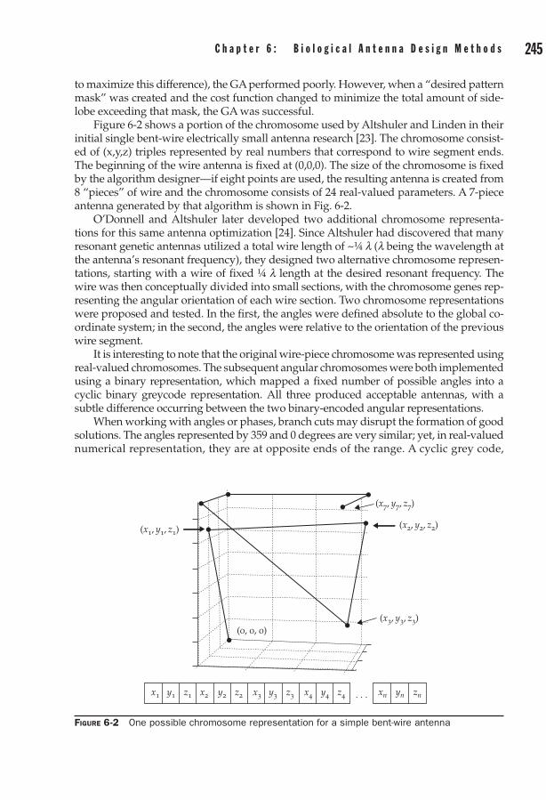
244 F r o n t i e r s i n a n t e n n a s : N e x t G e n e r a t i o n D e s i g n & e n g i n e e r i n g C h a p t e r 6 : B i o l o g i c a l a n t e n n a D e s i g n M e t h o d s 245
to maximize this difference), the GA performed poorly. However, when a “desired pattern mask” was created and the cost function changed to minimize the total amount of side-lobe exceeding that mask, the GA was successful.
Figure 6-2 shows a portion of the chromosome used by Altshuler and Linden in their initial single bent-wire electrically small antenna research [23]. The chromosome consist-ed of (x,y,z) triples represented by real numbers that correspond to wire segment ends. The beginning of the wire antenna is fixed at (0,0,0). The size of the chromosome is fixed by the algorithm designer—if eight points are used, the resulting antenna is created from 8 “pieces” of wire and the chromosome consists of 24 real-valued parameters. A 7-piece antenna generated by that algorithm is shown in Fig. 6-2.
O’Donnell and Altshuler later developed two additional chromosome representa-tions for this same antenna optimization [24]. Since Altshuler had discovered that many resonant genetic antennas utilized a total wire length of ~¼ l (l being the wavelength at the antenna’s resonant frequency), they designed two alternative chromosome represen-tations, starting with a wire of fixed ¼ l length at the desired resonant frequency. The wire was then conceptually divided into small sections, with the chromosome genes rep-resenting the angular orientation of each wire section. Two chromosome representations were proposed and tested. In the first, the angles were defined absolute to the global co-ordinate system; in the second, the angles were relative to the orientation of the previous wire segment.
It is interesting to note that the original wire-piece chromosome was represented using real-valued chromosomes. The subsequent angular chromosomes were both implemented using a binary representation, which mapped a fixed number of possible angles into a cyclic binary greycode representation. All three produced acceptable antennas, with a subtle difference occurring between the two binary-encoded angular representations.
When working with angles or phases, branch cuts may disrupt the formation of good solutions. The angles represented by 359 and 0 degrees are very similar; yet, in real-valued numerical representation, they are at opposite ends of the range. A cyclic grey code,
x1
(x1, y1, z1) (x2, y2, z2)
(x7, y7, z7)
(x3, y3, z3)(0, 0, 0)
xny1 yn znz1 x2 y2 z2 x3 y3 z3 x4 y4 z4 . . .
Figure 6-2 One possible chromosome representation for a simple bent-wire antenna

246 F r o n t i e r s i n a n t e n n a s : N e x t G e n e r a t i o n D e s i g n & e n g i n e e r i n g C h a p t e r 6 : B i o l o g i c a l a n t e n n a D e s i g n M e t h o d s 247
in which the Hamming distance between consecutive binary representations and the first-to-last binary representation is always 1, offers an attractive binary representation for phases and angular parameters. Transforming into sine and cosine space addresses this issue for real-valued representations, albeit at the expense of adding more parame-ters to the chromosome and thus the resulting search space.
Determining a successful chromosome design can be the most important and chal-lenging task in successfully applying GA optimization. As the entire success of a GA lies in the ability for good schema to eventually be merged together, it is vital that the chro-mosome design make this as easy as possible to accomplish.
6.2.1.3 Select ParentsParents for the next generation are selected based upon their cost. There are many differ-ent types of selection mechanisms; here we describe some of the more common ones. In the simplest selection mechanism, the top N chromosomes are used as parents, which are randomly selected from that subset. With thresholding, all chromosomes whose fitness exceeds a certain value are viable as parents, with random selection once again from that pool. In tournament selection, two or more candidate parents are selected randomly and the one from each pair with the highest fitness becomes a parent. In roulette-wheel selec-tion, candidate parents are allocated a fixed probability of selection, like a wedge on a roulette wheel. Parents with higher fitness are given larger wedges while lower-ranking parents have a smaller, but still finite chance of being selected. Once the probabilities are allocated, parents are then selected, based on which wedge a random number lies within (similar to spinning a roulette wheel). Note that tournament and roulette-wheel tech-niques may be used with the entire population or with only a higher-ranking subset of the population.
More complicated selection techniques include diversity, which considers not only the chromosomes’ fitnesses, but also the differences in numerical values between the param-eters comprising the chromosomes. This can be computed, in the simplest case, using least-mean squares (LMS) difference. The goal of diversity in selection is to avoid prema-ture convergence in a local minima, which occurs when top-performing chromosomes have all evolved around a local minima, thus having about the same input parameters. When diversity is included in selection, chromosomes which are not as good as the top-performers, but which are “good enough” and significantly “different” in parameter space are given a greater opportunity for selection than their figure of merit would warrant alone. Good enough may be defined as having a fitness exceeding some threshold or in the top half of the population; difference may be defined as the LMS difference in chromosome parameters as compared to the top performer(s). Diversity keeps a GA from prematurely converging in a local minima by allowing parents located near other minima a chance to also develop children. Note that diversity is more important in the early stages of the GA (when the search is more global) than during the latter stages (when we assume the GA chromosomes are close to the best global minima and a more local search is desired).
There is no firm requirement for uniqueness in the parents selected for recombina-tion. While this constraint can be applied within a GA, there is also something to be gained by allowing a parent to recombine with itself, i.e., using the same chromosome as the mother and father. This essentially allows a parent to pass a copy of itself directly to mutation. Depending on the shape of the response surface and mutation rate, this tech-nique can be useful during the end of the GA for “bouncing” down into the very bottom of a minimum.

246 F r o n t i e r s i n a n t e n n a s : N e x t G e n e r a t i o n D e s i g n & e n g i n e e r i n g C h a p t e r 6 : B i o l o g i c a l a n t e n n a D e s i g n M e t h o d s 247
The previously mentioned selection techniques have all considered only a single figure ofmerit.Inmultiple-objectiveGAs,severalfiguresofmeritarecomputedforeachchro-mosome and non-dominated Pareto fronts are created. Pareto points consist of those solutions to the problem for which further improvement in one objective causes aworseninginoneormoreotherobjectives.PointsalongaParetofrontareconsideredto be non-dominated, i.e., there is no other solution which simultaneously improves all objectives.InamultiobjectiveGA,non-dominatedchromosomesarerankedhighestforselection as parents. More parents may be selected, if necessary, by picking those chromo-somes along the second Pareto front (i.e., those which are only dominated by one other chromosome), and subsequent Pareto fronts. An excellent reference for understanding andimplementingmultipleobjectiveGAsisDeb’spaperontheNon-dominatedSortingAlgorithm II (NDSA-II) [21]. An antenna design application using the NDSA-II algorithm formultipleobjectives,inconjunctionwithgeneticprogrammingtechniques,isfoundin [25] and is summarized later in this chapter.
There are several techniques for constructing subsequent populations within a GA. When modeled strictly after nature, the entire population is replaced in each generation by children. Hence, the number of children created per generation is the entire popula-tion size. This total replacement unfortunately offers the possibility of losing some very good solutions and the best fitness in the population oscillates, rather than increasing steadily. However, one expects the peak of the oscillations to steadily increase over time.
6.2.1.4 MatingMating combines the parameters from parent chromosomes to create new and different offspring. The choice of the mating mechanism depends on whether the chromosome representation is binary or real-valued. Crossover combines two binary chromosomes to create two children. One or more points along the binary string are chosen at random and portions of the string between these points are copied from the mother and father chro-mosomes to create a child chromosome. As shown in Fig. 6-3, this technique can create more than one child per recombination; however, there is no requirement to generate and use all possible children.
Note that at least two crossover points should be used to avoid numerical bias at the ends of the string. Additionally, one may choose whether to allow crossover at any point within the string or only at gene boundaries, i.e., those boundaries between the binary integers representing each parameter. Crossover only at the gene boundaries acts to keep schema together, since the binary integer representing each parameter will transfer in its
1 1 1 1 1 1 1 11
11111
0 0
0 0 0 0 0 0
0 0 0 0000
0 0 0 0 0 0 0
Parent #1
Randomcross-overpoint #1
Randomcross-overpoint #2
Parent #2
Child #1
Child #2
Figure 6-3 Simple 2-point cross-over recombination with a binary string

248 F r o n t i e r s i n a n t e n n a s : N e x t G e n e r a t i o n D e s i g n & e n g i n e e r i n g C h a p t e r 6 : B i o l o g i c a l a n t e n n a D e s i g n M e t h o d s 249
entirety to the new child string. Crossover within a gene, however, essentially creates new binary genes in both children at that point. Depending on the binary to parameter mapping, these new binary genes may decode into parameters that are very different from either parent, effectively acting more like mutation of that parameter.
N-point binary crossover is a simple yet powerful method that has been used success-fully in many antenna optimizations. One recent real-world example was the genetic optimization of the USAF Weather Agency Digital Ionospheric Sounding System (DISS) transmit antenna. For this optimization, a binary grey-coded chromosome was used, with roulette-wheel selection of two parents and N-point crossover in recombination. The resulting antenna upgrade on Ascension Island showed stronger measured echoes off the ionosphere, with more layers being measured. The measurement error was re-duced by a factor of 10, reducing the critical frequency error from 16% to 1.6% [26], [27].
Uniform crossover is a general procedure that selects variables from each parent chromosome based on a mask, then places them in a new offspring chromosome. First, a random binary mask is created. A 1/0 in the mask column means the offspring receives the variable value from chromn m/ . If it has a 0/1, then the offspring receives the variable value in chromn m/ .
chrom v v v v v v v v
chrom m m m m m m m m= , , , , , , , ,1 2 3 4 5 6 7 8
mm v v v v v v v vn n n n n n n n n==
, , , , , , , ,1 2 3 4 5 6 7 8
0mask
, , , ,
0 1 0 0 1 0 1
1 2 3offspring = v v v vn n n n 44 5 6 7 8
1 2 3
v v v v
v v v vn n n n
m m m m
, , , ,
, , , ,offspring = 44 5 6 7 8v v v vm m m m, , , ,
Various techniques exist for recombining real-valued chromosomes. In the simplest crossover method, one or more random points are chosen in the parents, and the param-eters between these points are swapped between the two parents [28]. This technique transfers the parameters as a whole and does not generate any new parameters. Note that this method occurs only at the gene boundaries for continuous parameters, so gene al-terations only occur during mutation.
A more sophisticated method that seeks to combine salient information on the gene level to create new parameters intelligently is the blending method. Similar to the binary crossover method, one or more random crossover points are selected. The parameters between these points are not transferred in their entirety, but rather weighted and blend-ed to form new parameter values in the children. A random “mixing” variable, b, is cho-sen (usually between 0 and 1), and the new parameter values are blended such that
v v v v
v v v
m m m n
n n m
, , , ,
, , ,
[ ]
[
α α α α
α α
β
β
new
new
⇐ − −
⇐ + αα α− vn, ] (6-6)
where vm,α and vn,α are the parameters of the mother and father and vm,αnew
and vn,αnew are
the resulting blended parameters used in the children. Other parameters, which are not blended, can be swapped in their entirety, to create the final offspring. Note that, like the crossover method, multiple children may be produced from each recombination, but it is not required that all combinations be used.
A random choice of b between 0−1 guarantees that the result of the mix will be bounded by the values of the parents. While this eliminates the need to check resulting

248 F r o n t i e r s i n a n t e n n a s : N e x t G e n e r a t i o n D e s i g n & e n g i n e e r i n g C h a p t e r 6 : B i o l o g i c a l a n t e n n a D e s i g n M e t h o d s 249
parameters for correctness (i.e., valid values), it also makes it difficult to approach the endpoint of a parameter range. An extrapolating method allows b to exceed 1, so that values outside the range of the mother and father may randomly result from blending. However, this requires that parameters be checked for correctness prior to proceeding.
Note that this check for correctness can be applied either at the time of parameter cre-ation (i. e., as part of the mixing operation), or after the entire chromosome is generated, but prior to fitness evaluation. If performed as part of mixing, it is easy at this point to accom-plish another random mixing until a valid parameter is created. This is obviously more efficient than creating the entire chromosome only to discard it later on in the GA (prior to the fitness function) for having invalid values. However, the ability to check values for correctness at this point depends on the versatility of the GA engine being used.
Note also that there is no requirement to use only one b for weighting all the param-eters being mixed. Different bs may be randomly selected for each parameter to vary how much each parameter between the mother and father is combined. In a particular blend-ing method known as linear crossover, three children are created per recombination with predefined bs used [29].
A hybrid “quadratic-mixing” crossover technique was used in the electrically small genetic bent-wire antenna design research by Altshuler and Linden [23]. Three parents were selected using the roulette-wheel method and each gene was mated separately with a quadratic fit used to create the corresponding gene in the child. The resulting values were checked for correctness at time of creation. If the quadratic fit failed to produce a valid gene, a random point between two of the parents was used, i.e., mixing. If mixing still failed to produce a valid gene, the genes were only swapped.
6.2.1.5 MutationMutation is the third simple, yet powerful, mechanism that comprises the heart of the GA. The mutation operator randomly changes portions of the chromosome to introduce new genetic material into the population. Mutation is characterized by a mutation rate, which is the probability that a parameter receives a random modification. Like recombi-nation, the actual operator used for mutation may be different between binary chromo-somes and real-valued chromosomes.
The mutation rate determines the percent of bits or continuous parameters to be mutated. A randomly selected bit changes from a “0” to a “1” or from a “1” to a “0”. A randomly selected continuous parameter is replaced by another random or quasi-ran-dom value within the range of that parameter.
Simple GAs use a steady mutation rate, while more sophisticated approaches vary the mutation rate over time. For example, it may be desirable to initially start with a higher mutation rate to force a wider, more random, sampling of the response surface. Assuming that good schema start emerging within the population, this rate could then be decreased so that recombination becomes the dominant operator, which would allow these schema a chance to recombine with fewer random variations of their values. Others have had suc-cess with cycling the mutation rate over time, from high to low to high, etc. This technique essentially introduces periods where new genetic material is added rapidly to the popula-tion, but then the population is allowed to recombine and “cool off” to essentially pick out the good schema in this new material and determine how best to combine it.
Changes in the mutation rate can be fixed by a predetermined schedule based on generation number, or tied into convergence characteristics. For example, if the best solu-tion has not changed after a certain number of generations, this could be the trigger to increase and cycle the mutation rate to shake up the population.

250 F r o n t i e r s i n a n t e n n a s : N e x t G e n e r a t i o n D e s i g n & e n g i n e e r i n g C h a p t e r 6 : B i o l o g i c a l a n t e n n a D e s i g n M e t h o d s 251
Real-valued chromosomes offer additional mutation possibilities. Rather than select-ing a replacement value at random from the entire range of valid parameter values, it may be desirable to simply offset the existing parameter value randomly within a certain fixed amount. The technique is particularly applicable during the end-stages of the algo-rithm, where a good solution has been obtained but one is not certain if the bottom of the bowl, has been reached. While a purely random parameter selected from all possible pa-rameter values has a high probably of leaving that minimum, a small variation or “offset” from the parameter essentially creates a local search around the existing good value. One can envision decreasing this offset window as the GA progresses, thus transitioning from an initial global search of the response search to a local search around a good solution in the endgame of the GA.
Elitist techniques, on the other hand, preserve one or more of the best solutions with-in the population. With single elitism, only the best chromosome with the highest fitness is included in the subsequent generation; with multiple elitism, the top N solutions are pre-served. Taken to the extreme case, the entire population is preserved and only one chro-mosome added per generation, a technique that was successfully used by Thors, Stey-skal, and Holter in a GA used to design a fragmented wideband patch element [30]. The choice as to how many parent chromosomes to preserve and how they are selected (fixed percentage, thresholding) is one of the design considerations when developing a GA. In most cases, the number of children created is the quantity needed to bring the population back to the predefined size.
Another similar consideration is whether to impose uniqueness on the population, so that no duplicate chromosomes are created. This decision is often based upon the selec-tion mechanism. If the probability of choosing a chromosome is based strictly upon rela-tive fitness, then only one copy of an excellent chromosome is needed. However, if the selection mechanism is more random, multiple copies of that excellent chromosome are needed to ensure a greater probability of its selection.
6.2.1.6 ConvergenceIn the simplest case, a GA may be stopped after a predetermined fitness or number of generations is reached. The GA could also be stopped when no improvement has been seen in the best solution after a fixed number of generations. Note that this technique ap-plies best to elitist GAs, since oscillation is expected with nonelitist populations and this would be a difficult constraint to apply. Finally, if uniqueness is not enforced in the popu-lation, a stopping criteria might be that point when the entire population converges to one chromosome, or within some small deviation of the best chromosome.
6.2.2 Successful GA StrategiesThe authors have successfully used GAs to optimize many different antennas and have compiled some working wisdom that is presented in this section.
6.2.2.1 Minimize Cost Function Evaluations A GA calls the cost function many times. If the cost function takes considerable time to ex-ecute, then some steps for reducing the number of cost function evaluations include [28]:
1. Never evaluate the same chromosome twice! Keep a table of all chromosomes which have ever been proposed by the algorithm and their resulting figure of merit. Check this table for cached results prior to evaluating a chromosome: if it has already been evaluated, use the cached result.
250 F r o n t i e r s i n a n t e n n a s : N e x t G e n e r a t i o n D e s i g n & e n g i n e e r i n g C h a p t e r 6 : B i o l o g i c a l a n t e n n a D e s i g n M e t h o d s 251
2. Consider imposing uniqueness requirements on the population so that no duplicate chromosomes (i.e., identical twins) are allowed. In this case, if a new child results, which has already been evaluated, that child would be disallowed and another child created in its place. This has pros and cons, depending on your selection mechanism.
3. Define a “minimum solution granularity” or basically a round-off point at which two continuous values for the same gene position are considered equal. This technique prevents the algorithm from wasting time computing essentially the same result for the same input point, and is essential if one wants to impose uniqueness requirements upon a continuous value chromosome. (Otherwise, uniqueness will be defined by the numerical precision of one’s computational engine, resulting in chromosomes that are numerically “different” but essentially the same, as the numerical variations only exist within in the high-precision gene digits.)
4. Initially represent the parameters more coarsely than ultimately desired [31]. This has the effect of narrowing the initial global search space. As the GA progresses, the chromosome is then dynamically modified (either the minimum solution granularity changed for continuous valued genes, or more bits were added to a binary chromosome gene) to allow for a more fine representation. The allowable search area in the function space may be simultaneously reduced around known good areas. For relatively smooth response surfaces, these combined techniques allow the GA population to more quickly progress to relatively good solutions, before drilling down into even better, more finely tuned solutions. (Note that if one expects the response surface to be spiky, this technique is not advised.)
6.2.2.2 Don’t Evaluate Junk Chromosomes Many computational electromagnetic (EM) simulators assume some level of competency from their users. This is not going to be the case when random combinations of parame-ters and bizarre antenna configurations emerge from the GA. Depending on the EM tools used, various levels of preprocessing for correctness may be required. Bad chromosomes (i.e., those which would cause your EM simulator to produce incorrect and invalid re-sults without warning) need to be removed automatically (by your code) from the popu-lation prior to the cost function evaluation—otherwise they may become your solution!
While single invalid parameters can often be detected and removed prior to the EM simulation, the problem usually lies with combinations of parameters that are individu-ally correct but wrong when occurring together. For example, when the DISS transmit antenna was optimized, it was noted that, during preprocessing, the minimum distance betweenadjacentwireswasaconstraintthatneededtobecheckedtoavoid“sparking”[27]. Individually, all the wires were at valid heights, but taken together, some configura-tions were not electromagnetically feasible and needed to be removed, automatically, during the GA to avoid problems that the EM simulator would not have detected.
6.2.2.3 Hybrid Genetic Algorithms A hybrid GA starts with a GA and then hands the optimization off to a local optimizer [28]. The GA is good at finding the region of the global minimum but is extremely slow to get to the bottom. Usually, the GA runs until it slows down, then the local optimizer takes over. The continuous GA most easily couples to a local optimizer, since local

252 F r o n t i e r s i n a n t e n n a s : N e x t G e n e r a t i o n D e s i g n & e n g i n e e r i n g C h a p t e r 6 : B i o l o g i c a l a n t e n n a D e s i g n M e t h o d s 253
optimizers use continuous variables. In general, the hybrid GA performs quite well when compared to other local optimizer and GAs alone [32].
6.2.3 ExamplesOur first example is straightforward and is the design of a circularly polarized patch. The next two examples are much more complex and demonstrate the power of the GA.
6.2.3.1 Microstrip Patch DesignFigure 6-4 is a rectangular patch on an infinite substrate and ground plane that is de-signed for circular polarization at 10 GHz. There are six variables in the chromosomes, v v v v v v1 2 3 4 5 6
defined by
F F v L v Lx y x y, . ,( ) = ( ) =0 4 5 6 position of probe feed
L vx y, ,= + =λ λ4 41 2 patch length in x and y directions
hmm round v
mm round v= >
≤
3 15 0 5
1 575 0 53
3
. .
. .
= substrate thickness
ε = >
≤
=
2 33 0 5
2 2 0 54
4
. .
. .
round v
round v relative dielectric constant of the substrate
where l in mm.The cost function is computed using the method of moments-and-returns the maximum of three computed terms
cost =−+
∠ − ∠ −max| | | |
| | | |,| | ,|
E E
E EE Eθ ϕ
θ ϕθ ϕ
π2
ss11|
(6-7)
where
E = + =E Eθ φθ φ) )
electric field
s11 = reflection coefficient
The first two terms in (6-7) are zero for circular polarization, because the two components of the electric field have the same magnitude and are 90° of phase. The magnitude of the
h yx
z
LxLy
Fy Fx
ε
Figure 6-4 Diagram of the optimized circularly polarized patch antenna

252 F r o n t i e r s i n a n t e n n a s : N e x t G e n e r a t i o n D e s i g n & e n g i n e e r i n g C h a p t e r 6 : B i o l o g i c a l a n t e n n a D e s i g n M e t h o d s 253
reflection coefficient is zero when the patch impedance 50 Ω. A circularly polarized, per-fectly matched patch has cost = 0. The best chromosome resulted in the following design values:
F F mm mmx y, . , .( ) = ( )1 18 2 96
L L mm mmx y, . , .= 8 62 9 98
h mm= 1 575.
ε = 2 2.
The patch is right-hand circularly polarized with an axial ratio of 1.009, s11 = 0.012, and directivity of 6.97 dB. The GA, with a population size of 12 and mutation rate of 5%, reduced the cost very quickly in the first few generations, then much slower, as shown in Fig. 6-5.
6.2.3.2 Optimizing a Simple Parasitic Superdirective ArrayRecently, Southall and O’Donnell used two different GAs to optimize the separation and operating frequency of a two-element parasitic superdirectional array [33], [34], as shown in Fig. 6-6a, to achieve the highest end-fire directivity. The antenna element configuration is fixed, and only the separation between the elements and the operational frequency varied. However, it is a multimodal problem with two almost equal minima (shown in Fig. 6-6b), depending on whether the parasitic acts as a director or reflector, which de-pends on the operating frequency of the array.
The antenna element used for this array was planar and was moderately small, hav-ing a height of 0.146 l at the resonant frequency of a single, isolated element. The input function space was exhaustively sampled, as shown in Fig. 6-6b, to determine the largest possible gain. This was feasible for this simple two-dimensional example, since the anten-nas consist of thin wires in free space over an infinite ground plane, which could be very efficiently simulated using the Numerical Electromagnetics Code 4 (NEC4) [51].
0.5
0.4
0.3
0.2
0.1
00 50 100 150 200
Generation
Cos
t
Figure 6-5 Convergence of the GA for the circularly polarized patch antenna

254 F r o n t i e r s i n a n t e n n a s : N e x t G e n e r a t i o n D e s i g n & e n g i n e e r i n g C h a p t e r 6 : B i o l o g i c a l a n t e n n a D e s i g n M e t h o d s 255
At a spacing of 8.9 mm and a frequency of 849 MHz, the array has a reflector lobe with a gain of 10.262 dB, which is the largest possible gain (global minimum in Fig. 6-6b). A director lobe with a gain of 10.154 dB occurs at 14 mm and 834 MHz (local minimum) and is, therefore, a local minimum close to the global minimum of −10.262 dB. The upper valley region near the global minimum has an extremely flat floor. For example, along the valley bottom from 8 to 10 mm, the spacing changes by 25% and the frequency by 1% while the gain changes by less than 0.05%. This makes it extremely difficult for any algo-rithm to give very precise values for the spacing and frequency, which yield the absolute minimum in the negative of the gain.
For both GAs, the chromosome consisted of two genes with continuous parameters representing the element separation (5−60 mm) and the operating frequency (800− 900 MHz). A Latin hypercube [45] technique was used to establish an initial population of Nipop chromosomes, which sampled the function space. Note that the initial population contained twice as many chromosomes as the population of successive generations to allow for adequate sampling of the response surface. Following the evaluation of this initial population, the bottom half (the poorer performers) were discarded, leaving the population with Npop = Nipop/2 chromosomes [9], i.e., a subset consisting of the best samples.
In the first simple GA, the top Npop/2 chromosomes are used for mating and the bottom Npop/2 chromosomes are discarded. Roulette wheel (a.k.a., weighed random pairing) was used for selection. Children were produced with one-point crossover (since there are only two parameters), with blending of some parameters (using the random mixing variable b, which varied between 0−1) and swapping off the rest.
This GA also preserved the top Npop/2 chromosomes in the next generation; however, mutation was performed not only on the children, but also on the parents, except for the
0.05
890900
880870860850
840830820810
80010 15 20 25 30 35 40 45 50 55 60
Separation (mm)
Local MinimaGlobal
Minimum
0.04
0.03
0.02
0.01
00 0.01 0.02
0
0.01
Y (mete
rs)
Z (m
eter
s)
Freq
uenc
y (M
Hz)
Two-element parasitic arrayTwo-dimensional response surface
Directivity as a function ofseparation and frequency
Min. function value = –10.262 at [8.9, 849]
(a) (b)
Figure 6-6 (a) Two-element parasitic superdirective array and (b) associated function space

254 F r o n t i e r s i n a n t e n n a s : N e x t G e n e r a t i o n D e s i g n & e n g i n e e r i n g C h a p t e r 6 : B i o l o g i c a l a n t e n n a D e s i g n M e t h o d s 255
best individual. This resulted in a single elitist population. Mutation rates between 10% and 70% were tested, with mutation selecting a total random value for the gene within the valid parameter bounds (versus an offset value).
Four different stopping criteria were initially considered simultaneously:
1. Limit of 100 total number of generations
2. Number of cost function calls exceeds 500
3. No change in best fitness after 1/5 of the limit on the total number of generations, i.e., 20 generations (stagnation)
4. 7/8 of the genes in the mating pool are identical (lack of diversity).
Note that conditions 1 and 2 do not indicate convergence, they simply quit after a fixed amount of time or computation.
To create a second “enhanced” GA, O’Donnell incorporated some of the advanced GA techniques described in this chapter. These techniques were selected to promote genetic diversity and avoid premature convergence. The resulting algorithm turned out to be “robust” [2] for this particular problem in that, once tailored, the algorithm consistently found the global minimum.
The techniques which enhanced this particular GA included:
• Varying the mutation rate (increasing or decreasing) as the algorithmprogressed
• Varyingthemutationtypefromtherandomgenereplacementtooffsetting.
• Varyingtheamountofoffsetmutation(fromhighertolower)asthealgorithmprogressed
• Applying minimum solution granularity and uniqueness to ensure that noduplicate chromosomes (within the minimum solution granularity) were allowed. Chromosomes were checked during creation and duplicates were reconstructed.
• Employmentofelitism,i.e.,theparentsmaintainedinthepopulationwerenotmutated
• Tournamentselection,ratherthanroulettewheel.
In order to implement the previous strategies more effectively, the input range for each parameter was normalized to range from 0–1. Since a diverse population was auto-matically maintained by the enhanced algorithm, population diversity was not a valid stopping criteria for termination of the algorithm. Only total number of generations, total number of function calls and stagnation were used.
Figure 6-7 shows a comparison of the simple GA (called “textbook” in the figure) to the enhanced GA for a total number of cost function calls. After tuning both algorithms, the enhanced GA algorithm typically converged to less than 0.05% difference from the global minimum within 500 function calls. Southall and O’Donnell also note in [33] that the enhanced GA converged 100% to the exact global minimum after 100 populations, albeit with more cost function calls.
Note that the mutation rates annotated on Fig. 6-7 are extremely high for a typical GA. However, as seen in Fig. 6-6b, the response surface for this problem has a very flat and curved bowl around the global minimum. Southall and O’Donnell note that, once

256 F r o n t i e r s i n a n t e n n a s : N e x t G e n e r a t i o n D e s i g n & e n g i n e e r i n g C h a p t e r 6 : B i o l o g i c a l a n t e n n a D e s i g n M e t h o d s 257
within this region, there was essentially no single-parameter inheritance between good parents. Once in the bowl “both a change in frequency and a change in separation are required to move from one good point to a better point; thus mating two “good” par-ents while blending only one of the genes does not result in a better design (higher directivity)” [33].
Therefore, the tuned enhanced GA utilized a lower mutation rate with a large offset amount in the early generations, which allowed for wider global exploration to rapidly locate the bowls of the function. Transitioning later to a higher mutation rate, but with associated smaller mutation offsets, allowed the algorithm to then randomly bounce around the bowls to ultimately determine the global minimum. The high mutation rate, but with only a small offset, increased the chances that both parameters would vary si-multaneously by a small amount, which was essential for traversing the relatively flat valley to the global minimum.
6.2.3.3 Antenna PlacementInthisexample,aGAisusedtofindanoptimallocationforanIEDjammerantennaonaHumvee.Thegoalofthejammeristoprojectamaximumamountofpowerontheroadin front of the Humvee where a suspected IED is hidden. The commercially available software XFdtd [36] was used to model the Humvee and calculate the fields radiated by the antenna [37], [38]. The GA is written in C++ and interfaces with the XFdtd cost func-tion through XFdtd’s Scripting API. XFdtd uses Feature Based Modeling (FBM) that al-lows relative coordinate system definitions among parts in a model.
This GA has a population size of 8 and a mutation rate of 15%. A chromosome con-tains the region and the location on that region for antenna placement. Figure 6-8 shows the six areas available on the vehicle for placement of the antenna. Each cost function evaluation calls a script function that executes the calculation engine, calculates the cost (antenna pattern, impedance, bandwidth, etc.), and passes that value back to the GA as the cost. The GA ran 13 generations. The optimal location found is depicted in Fig. 6-9 with the electric field depicted in Fig. 6-10. It turns out that the optimal location is on the
1
0.9
0.8
0.7
0.6
0.5
0.4
0.3
0.2
0.1
00 100 200 300 400 500 600
Total Number of Cost Function Calls
Textbook GA: Npop = 12; Mutation = 50%Enhanced GA: Npop = 16; Mate 50%; Keep 25%Initial mutation = 60%; Rate increment = 1.02; Final = 100%Initial rate sigma = 0.6; Final rate sigma = .05
% D
iffe
renc
e fr
om G
loba
l Min
imum
Figure 6-7 Comparison of performance between a simple GA and one enhanced with additional features

256 F r o n t i e r s i n a n t e n n a s : N e x t G e n e r a t i o n D e s i g n & e n g i n e e r i n g C h a p t e r 6 : B i o l o g i c a l a n t e n n a D e s i g n M e t h o d s 257
R6 R4
R3R5R1
R2
Figure 6-8 Allowable areas for antenna placement on vehicle
Figure 6-9 Optimum antenna placement on vehicle
Figure 6-10 Fields radiated by antenna when placed on the rear of the vehicle, the frontmost position on the vehicle, and the optimum location on the vehicle.

258 F r o n t i e r s i n a n t e n n a s : N e x t G e n e r a t i o n D e s i g n & e n g i n e e r i n g C h a p t e r 6 : B i o l o g i c a l a n t e n n a D e s i g n M e t h o d s 259
front hood and not on the front bumper. The second best location is on the driver-side front bumper.
6.2.3.4 Low-Profile, Broadband, Shorted Monocone AntennaA GA was used to design a low-profile, wideband, vertically polarized monocone to be used on an unmanned aerial vehicle (UAV) or airplane [39]. A rough design of a top hat monocone with shorting pins was optimized using a GA with a population size of 8 and mutation rate of 15%. The antenna height, diameter, shorting pin locations, number of shorting pins, and top hat size were optimization parameters. Figure 6-11 is a model of the antenna. After optimization, it is λ / .14 7 tall at 800 MHz and λ / 5 tall at 2.4 GHz. Figure 6-12 is a plot of the reflection coefficient (S11) from experimental measurements and computed results. The antenna bandwidth (SWR < 2) is from 800 MHz to 2.4 GHz.
6.3 Genetic ProgrammingUp to now, we have only considered chromosomes which contain encoded antenna de-sign parameters. In genetic programming, we consider chromosomes that contain combi-nations of “instructions” (or programming steps) and parameters, which together describe an antenna design. The standard fixed-length linear-chromosome structure commonly
Feed
Shorting pins Ground plane
Figure 6-11 Final antenna design, which was used as the experimental antenna
0.5 0.75 1 1.25 1.5Frequency (GHz)
Measured
Computed
2.4 GHz800 MHz
0
–5
–10
–15
–20
–25
S 11
(dB
)
1.75 2 2.25 2.5
Figure 6-12 S11
the experimental antenna compared to MWS
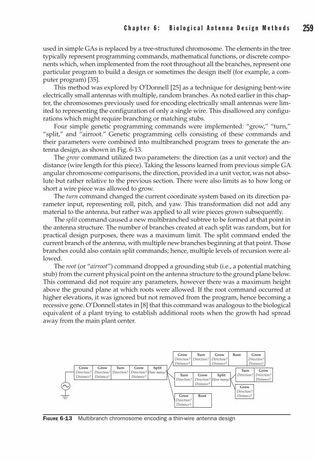
258 F r o n t i e r s i n a n t e n n a s : N e x t G e n e r a t i o n D e s i g n & e n g i n e e r i n g C h a p t e r 6 : B i o l o g i c a l a n t e n n a D e s i g n M e t h o d s 259
used in simple GAs is replaced by a tree-structured chromosome. The elements in the tree typically represent programming commands, mathematical functions, or discrete compo-nents which, when implemented from the root throughout all the branches, represent one particular program to build a design or sometimes the design itself (for example, a com-puter program) [35].
This method was explored by O’Donnell [25] as a technique for designing bent-wire electrically small antennas with multiple, random branches. As noted earlier in this chap-ter, the chromosomes previously used for encoding electrically small antennas were lim-ited to representing the configuration of only a single wire. This disallowed any configu-rations which might require branching or matching stubs.
Four simple genetic programming commands were implemented: “grow,” “turn,” “split,” and “airroot.” Genetic programming cells consisting of these commands and their parameters were combined into multibranched program trees to generate the an-tenna design, as shown in Fig. 6-13.
The grow command utilized two parameters: the direction (as a unit vector) and the distance (wire length for this piece). Taking the lessons learned from previous simple GA angular chromosome comparisons, the direction, provided in a unit vector, was not abso-lute but rather relative to the previous section. There were also limits as to how long or short a wire piece was allowed to grow.
The turn command changed the current coordinate system based on its direction pa-rameter input, representing roll, pitch, and yaw. This transformation did not add any material to the antenna, but rather was applied to all wire pieces grown subsequently.
The split command caused a new multibranched subtree to be formed at that point in the antenna structure. The number of branches created at each split was random, but for practical design purposes, there was a maximum limit. The split command ended the current branch of the antenna, with multiple new branches beginning at that point. Those branches could also contain split commands; hence, multiple levels of recursion were al-lowed.
The root (or “airroot”) command dropped a grounding stub (i.e., a potential matching stub) from the current physical point on the antenna structure to the ground plane below. This command did not require any parameters, however there was a maximum height above the ground plane at which roots were allowed. If the root command occurred at higher elevations, it was ignored but not removed from the program, hence becoming a recessive gene. O’Donnell states in [8] that this command was analogous to the biological equivalent of a plant trying to establish additional roots when the growth had spread away from the main plant center.
GrowDirection?Distance?
GrowDirection?Distance?
GrowDirection?Distance?
GrowDirection?Distance?
GrowDirection?Distance?
GrowDirection?Distance?
GrowDirection?Distance?
GrowDirection?Distance?
Root
RootGrowDirection?Distance?
GrowDirection?Distance?
TurnDirection? Turn
Direction?TurnDirection?
TurnDirection?
SplitHow many?
SplitHow many?
Figure 6-13 Multibranch chromosome encoding a thin-wire antenna design

260 F r o n t i e r s i n a n t e n n a s : N e x t G e n e r a t i o n D e s i g n & e n g i n e e r i n g C h a p t e r 6 : B i o l o g i c a l a n t e n n a D e s i g n M e t h o d s 261
The antenna structures were optimized along several Pareto parameter fronts using theNon-dominatedSortingGeneticAlgorithmII(NSGA-II)multiobjectiveevolutionaryalgorithm [6]. Three figures of merit were used: electrical size (the radius in wavelengths of the minimal hemisphere which fully encloses the antenna) voltage standing wave ratio (VSWR), and antenna quality factor (Q). Recombinations were implemented by swap-ping random portions of the genetic program tree between random crossover points. Mutations were implemented by adding, deleting, or swapping programming com-mands or mutating the values of command parameters.
Genetic programming offers several attractive features for those interested in geneti-cally optimized antenna designs. Because the chromosome is allowed to dynamically al-ter and split, many different designs may be explored within one GA. Structures having significant physical differences may still be combined, even though their tree-like chro-mosomes are radically different from each other. Perhaps most importantly, many of the prior design decisions that are inherent when developing a simple linear-chromosome GA (such as “how many wire pieces,” “how many segments,” “how long the total wire length”) are no longer limiting factors. However, the unrestricted design combinations that are possible with a genetically programmed antenna greatly increase the size of the response surface to be searched. Therefore, there is once again the natural tradeoff be-tween how flexible one wishes to be in the design and how long one wishes to design.
6.4 Efficient Global OptimizationEfficient Global Optimization (EGO) is an evolutionary computation (EC), data-adaptive algorithm, which can be useful for problems with very expensive cost functions [41], [42]. Many evolutionary algorithm techniques require large numbers of cost function evalua-tions. This can be prohibitive when using the complex computational electromagnetic (CEM) simulations required for modern antenna design [43] where the evaluation of each design can take significant resources.
Like GAs, EGO performs both global and local searches simultaneously to explore the function space and to avoid becoming trapped in local minima. The algorithm mod-els the cost function (response surface) using the DACE predictor (Design and Analysis of Computer Experiments) [44]. The model is refined in areas which warrant further exploration, either because they are close to known good areas (local search) or because they have been insufficiently explored and exhibit uncertainty (global search). In each iteration only a single design point is evaluated using the expensive cost function. A GA evaluates the cost function many times for numerous proposed solutions. The goal of EGO is to spend less time evaluating the cost function and instead to use very fast, inex-pensive calculations (the DACE predictor) to model the response surface.
The response surface is fit using a stochastic model, which captures how the function typically behaves [41]. One behavior might be how much the function tends to change as we change a certain input variable. Using the stochastic model one can develop figures of merit for selecting new design points (also called data points or sample points). The tech-nique is a very powerful, effective, and efficient method for selecting new design points. The algorithm begins with a relatively small initial set of points and then the following steps are performed iteratively:
1. Determine a set of correlation parameters using maximum likelihood
2. Select the next design point to evaluate
3. Test for convergence.

260 F r o n t i e r s i n a n t e n n a s : N e x t G e n e r a t i o n D e s i g n & e n g i n e e r i n g C h a p t e r 6 : B i o l o g i c a l a n t e n n a D e s i g n M e t h o d s 261
We first describe the stochastic process model followed by a detailed description of the steps used in the algorithm. We then describe an antenna design example, the para-sitic superdirective array (PSA) antenna, and use it to illustrate the usefulness of EGO in antenna design optimization. Finally, we compare the performance of EGO with that of two different kinds of GAs used to optimize the same antenna design.
6.4.1 The DACE Stochastic Process ModelThe DACE stochastic process model was originally described in the paper “Design and Analysis of Computer Experiments,” by Sacks, et al. [44]. The response surface is sam-pled at n design points. The initial number of points is chosen to be about 10k where k is the dimensionality of the problem. In [41], [44] n = 11k-1 was suggested. For multidimen-sional problems, we use a space-filling technique called the Latin hypercube [45] for se-lecting the initial set of points in the k-dimensional input function space.
The n scalar values y(i), i = 1,2 … n, of the cost function are represented by the data vector y which is a function of input vector x. Input vector x contains the n design vectors x(i) for i = 1,2 … n. Each design vector has k independent design parameters.
y = y y y nnx
( ) ( ) ( )...1 21 (6-8a)
x( ) ( ) ( ) ( )...i i ik
ik x
x x x= 1 2 1i = 1, 2… n (6-8b)
For example, if the problem were one dimensional, i.e., k = 1, there would be a single in-put variable (also called input parameter or input factor), x, sampled at n points, and x would be an n × 1 column vector.
The DACE model assumes a constant regression term, μ, as shown below for the model representing each sample data point:
y y i ni i i( ) ( ) , , ...,( ) ( ) ( )x x= = + =µ ε 1 2 (6-9)
The error term, ε( )( )x i , is assumed to be normally distributed with zero mean and with process variance σ2 (see 6-15).
In electromagnetic computer simulations, the response is deterministic, i.e., running the code with the same input values will yield identical results. Therefore, the error term does not represent a random measurement error but the uncertainty about the outcome until we actually perform the simulation. The error terms are, however, assumed to be correlated from one design point to another. The correlation is assumed to be higher when design vectors x( )i x( )j are closer and lower when they are farther apart. The cor-relation is therefore related to the distance between points in the input function space. A weighted distance formula (not a simple Euclidean distance) is used. The weights in the distance formula are the correlation parameters, qh, in (6-10) below.
d x xi jh h
ihj p
h
kh
( , )( ) ( ) ( ) ( )x x = −=
∑θ1
. (6-10)
Correlation parameter qh measures the importance (or activity) of input parameter h. Larger values mean that the parameter is more important or active. The correlation parameter 1 ≤ ph ≤ 2 in the exponent is related to the smoothness of the function in input parameter direction h. Values of ph near 1 correspond to less smooth functions while values near 2 correspond to smoother functions [41], [44], [46]. We have used ph = 2 and found it to work well. Equations (6-9), (6-10), and (6-11) represent the DACE stochastic process model.

262 F r o n t i e r s i n a n t e n n a s : N e x t G e n e r a t i o n D e s i g n & e n g i n e e r i n g C h a p t e r 6 : B i o l o g i c a l a n t e n n a D e s i g n M e t h o d s 263
The correlation between errors at x(i) x(j) is then calculated from [41]:
Corr di j i jε ε( ), ( ) exp ( , )( ) ( ) ( ) ( )x x x x = − . (6-11)
We fit the response surface using the DACE predictor [41], [42]. Let x* be an arbitrary input point where the value of the response surface is unknown (see Fig. 6-14 below for a one-dimensional example). The DACE predictor at x* is given by
ˆ( *) ˆ ( ˆ ),y x r R y 1= + ′ −−µ µ1 (6-12)
where 1 is a column vector of n ones and R is an n × n error correlation matrix whose (i, j) entry is given by (6-11). The column vector rnx1 is the correlation between x* and all n data points. The ith element of r is given Corr [e(x*), e(x(i))], i = 1, 2, ...n. The DACE predictor interpolates the data, i.e., it yields the known values of y(x) at the sample points. The approximation in (6-12) requires only inexpensive, fast, matrix operations unlike the evaluation of the expensive cost function. For ph = 2, it was shown in [42] that the approxi-mation uses radial basis functions.
6.4.2 Estimation of the Correlation ParametersThe first step in the iterative loop of the algorithm is to estimate the parameters qh for h = 1,2 … k. These parameters are estimated by finding values of qh that maximize the likelihood of the sampled data. The parameters are therefore tuned to the data, which is why the algorithm is data adaptive. The sample likelihood function is given by [41]:
L(μ, s2) = 1
2 22 2 2 1 2
1
( ) ( ) det( )exp
( ) ( )
π σ
µ µσn n R
y 1 R y 1− − ′ −−
22
(6-13)
y(x)
fmin
0x
s = standard errorof prediction
(x) = DACEpredictor
y(x) Y = N( , s2)
x*
Sampled points
(a) (b)
0
sy(x*)ˆ
y
y
y
Y
fmin
fmin – Y > 0
Figure 6-14 (a) The uncertainty in the value of the function at arbitrary x* is represented by the random variable Y = N( y (x*),s2). (b) Detail showing the improvement at x*, which is also a random variable. Recall that I(x*) = max(f
min − Y, 0).

262 F r o n t i e r s i n a n t e n n a s : N e x t G e n e r a t i o n D e s i g n & e n g i n e e r i n g C h a p t e r 6 : B i o l o g i c a l a n t e n n a D e s i g n M e t h o d s 263
The dependence of the likelihood function on the correlation parameters comes from the correlation matrix R, where det(R) is the determinant of R. If we had values for the cor-relation parameters we could calculate R and find closed form expressions for estimates of μ and s (maximum likelihood estimates or MLE) as follows [41]:
ˆ ( )( )
µ = ′′
−
−1 R y1 R 1
1
1 (6-14)
and
ˆ ( ˆ ) ( ˆ )σ µ µ21
= − ′ −−y 1 R y 1n
(6-15)
Using these values for μ and s in (6-13) gives the concentrated likelihood function (CLF). The log of the CLF is maximized with respect to correlation parameters qh using a Nelder-Mead downhill simplex technique [34] to obtain maximum likelihood estimates of the k correlation parameters.
6.4.3 Selecting the Next Design Point Jones [41] introduced a figure of merit called expected improvement, which balances local and global search and is the heart of the EGO algorithm. The expected improvement is calculated using the mean squared error of the DACE predictor called the standard error of prediction given by
s2 2 11
2
11
1( )x r R r
1 R r
1 R 1= − ′ +
− ′( )′
−−
−σ
(6-16)
The error is reduced by the second term in the brackets since x is correlated with the cur-rent sample points and is increased by the third term, since μ is not exact but is only esti-mated from the data. The prediction error is zero at the sample points.
We define a new random variable Y which is normally distributed with a mean value of y(x) and variance s2(x) defined in (6-12) and (6-16), respectively [41]. Y models our uncertainty about the value of the cost function. This uncertainty at arbitrary point x* is shown in Fig. 6-14. Recall that the simulation is deterministic; we simply do not know the deterministic outcome at x* until the simulation is performed, thus the uncertainty.
Let f y y y nmin
( ) ( ) ( )min[ ]= 1 2 K be the current best (minimum) cost function value. Formally, the improvement is given by
I f Y( *) max( , )minx = − 0 . (6-17)
Since Y is a random variable, I(x*) is a random variable so we take the expected value of I(x*), which can be expressed in closed form [41] as follows:
E I f yf y
ss
f( *) ( ˆ )
ˆmin
min minx = −−
+
−Φ ϕ
ˆys
, (6-18)
where ϕ(z) is the normal probability density function and Φ(z) is the normal probability distribution function. Using y(x*) and s(x*) over all x* to evaluate E[I(x*)], we find where the expected improvement is maximized and take that x*as the new design point.

264 F r o n t i e r s i n a n t e n n a s : N e x t G e n e r a t i o n D e s i g n & e n g i n e e r i n g C h a p t e r 6 : B i o l o g i c a l a n t e n n a D e s i g n M e t h o d s 265
6.4.4 Convergence The final step is the implementation of a stopping rule or convergence criterion. Expected improvement provides a simple and effective criterion. One variation is to take the absolute value of the expected improvement, | E[I(x*)] |, at the new design point. If it is less than 1% of fmin (the current minimum value of the cost function), then stop. Obviously, one could choose a factor less than 1% and we have experimented with decreasing the criterion to obtain better accuracy; however, this increases the number of expensive function calls.
Alternatively, we can stop the algorithm after a set number of iterations. Using the total number of iterations as a stopping criterion prevents the algorithm from running extensively (trying to refine the response surface), while allowing it to drill deeper into minima than would otherwise occur when a larger value for the expected improvement is used as a stopping criterion.
If the stopping criterion is not met, we add the new design point to the data set and increase n by one. The algorithm then estimates correlation parameters using the n + 1 data points, i.e., all of the previous sample points plus the new data point. Iteration con-tinues until the convergence criterion is met.
With evolutionary design optimization techniques it is perhaps more realistic, and practical, to terminate algorithms based on performance criteria, i.e., where the current value of the cost function satisfies the design specification(s). This could replace artificial, and often arbitrary, convergence criteria.
6.4.5 Comparison of EGO and GA Design Optimization The EGO algorithm was used in the example presented in Section 6.2.3.2 to optimize the antenna design [42], [33], [53]. We compare EGO with the two different kinds of GA implementations used to optimize the same antenna design (Section 6.2.3.2). The num-ber of cost function calls is used as a figure of merit. In Fig. 6-15 we show the accuracy of the three algorithms in predicting the known global minimum versus the number of evaluations of the cost function required. All three algorithms consistently estimate the global minimum near 8.9 mm and 849 MHz. Note that all three algorithms were extremely accurate with prediction errors of much less than 1% of the global mini-mum. The EGO algorithm performed well and required fewer cost function calls than the GAs. The error bar for EGO (the spread in converged gain for the 15 different initial data sets) at slightly more than 100 function calls is remarkably small. Note also that with enough function calls (in a GA each generation requires many cost function calls) the Enhanced GA can predict the global minimum with arbitrary accuracy, as dis-cussed in Section 6.2.3.2.
6.5 Particle Swarm OptimizationEdward and Kennedy introduced particle swarm optimization (PSO) [55] based on the social behavior of animals, such as bird flocking or fish schooling. PSO has a random population matrix like the GA, but the rows in the matrix are called particles instead of chromosomes. Particles contain variable values and have a velocity as they move on the cost surface. The particles update their velocities and positions based on the local and global best solutions.
v v r p pm n m n m n m, , , ,new old local best= + × × −l1 1 nn m n m nr p pold global best old( ) + × × −( )l2 2 , , (6-19)

264 F r o n t i e r s i n a n t e n n a s : N e x t G e n e r a t i o n D e s i g n & e n g i n e e r i n g C h a p t e r 6 : B i o l o g i c a l a n t e n n a D e s i g n M e t h o d s 265
p p vm n m n m n, , ,new old new= + (6-20)
where
vm n, = particle velocity
pm n, = particle variables
r r1 2, = independent uniform random numbers
l l1 2 2= = =learning factors
pm n,local best best local solution=
pm n,global best best global solution=
The PSO algorithm finds new particles by updating the velocity vector for each particle and adding it to the previous particle position. Velocity updates are based on the best global solution associated with the lowest cost ever found by a particle, as well as the best local solution associated with the lowest cost in the present population. When the best local solution has a cost less than the cost of the current global solution, it replaces the best global solution. The constant l1 is the cognitive parameter, and the constant l2 is the social parameter.
PSO is capable of optimizing the same types of antenna designs as the GA. Many antenna design applications appear in the literature [56]–[61].
0 100 200 300 400 500 6000
0.1
0.2
0.3
0.4
0.5
0.6
0.7
0.8
0.9
1
Total Number of Cost Function Calls
% D
iffer
ence
from
Glo
bal M
inim
um
EGO: Max expect. improv. < .001% of fmin
EGO: with endgame – linearly decreasing ratio
Textbook GA: Npop = 12; Mutation = 50%
Enhanced GA: Npop = 16; Mate 50%; Keep 25%Initial mutation = 60%; Rate increment = 1.02; Final = 100%Initial rate sigma = 0.6; Final rate sigma = .05
Figure 6-15 Comparison of three design optimization algorithms. Error bars represent slightly different predicted gains at convergence for 15 runs (each run uses a different set of 21 initial data points) [22]. The ordinate represents the percent difference between the converged gain (EGO, Textbook GA, or Enhanced GA) and the known global minimum of −10.262 dB.

266 F r o n t i e r s i n a n t e n n a s : N e x t G e n e r a t i o n D e s i g n & e n g i n e e r i n g C h a p t e r 6 : B i o l o g i c a l a n t e n n a D e s i g n M e t h o d s 267
6.6 Ant Colony OptimizationAnt colony optimization (ACO) is a global search optimization method that is based on the behavior of ant colonies in obtaining food and carrying it back to the nest. Ants wan-der around looking for food. They emit a pheromone (chemical) along their trail from the food to home. Other ants follow this pheromone trail to the food source and also emit a pheromone as they do so. When ants pick a shorter path to the food, a stronger trail of pheromone develops faster than on a longer path. The stronger pheromone (shortest path) attracts more ants until the shorter path eventually becomes dominant. These pher-omones also evaporate slowly with time. This decreases the probability of taking paths toward finished food sources.
ACO algorithms were originally designed to solve the traveling salesperson problem, because this problem closely resembles finding the shortest path to a food source [62]. ACO results in premature convergence to a local optimal solution unless pheromone evaporation is implemented: a solution disappears after a period of time.
The probability that ant k will travel from city m to city n is given by
pd
dmnk mn
amnb
mqa
mqb
q
= ∑τ
τ/
/ (6-21)
where
t = pheromone strength q = cities on tour k that come after city m a = pheromone weighting; when a = 0, then closest city is selected b = distance weighting; when b = 0, then distance between cities is ignored.
Short paths with high pheromone have the highest probability of selection. On the initial paths, pheromone is laid on inefficient paths. Consequently, some of this pheromone must evaporate in time or the algorithm will converge on an inefficient path. Early trials of ACO found that an elitist strategy is as important as it is with GAs. As a result, the pheromone along the best path found so far by the algorithm is given some weight in calculating the new pheromone levels. The pheromone update formula is given by [63]
τ ξ τ τ ετmn mn mnk
k
N
mn= −( ) + +=
∑11
antselite (6-22)
where
τmnk k= pheromone laid by ant between city mm nand city
ξ = pheromone evaporation constant ε = elite path weighting constant τmn
elite = laid on the best path found by the algorithm to this point.
ACO is not as versatile for antenna design as the GA or PSO. It has found some use for antenna designs, however [64]-[66].

266 F r o n t i e r s i n a n t e n n a s : N e x t G e n e r a t i o n D e s i g n & e n g i n e e r i n g C h a p t e r 6 : B i o l o g i c a l a n t e n n a D e s i g n M e t h o d s 267
ReferencesH. Schwefel, [1] Evolution and Optimum Seeking, New York: John Wiley, 1995. D. E. Goldberg, [2] The Design of Innovation: Lessons from and for Competent Genetic Algorithms, Kluwer Academic Publishers, Boston, MA. 2002.J. H. Holland, [3] Adaptation in Natural and Artificial Systems, Ann Arbor: The University of Michigan Press, 1975.R. L. Haupt, “An introduction to genetic algorithms for electromagnetics,” [4] IEEE Antennas and Propagation Magazine, vol. 37, issue 2, pp. 7–15, Apr 1995.R. L. Haupt, and D. H. Werner, [5] Genetic Algorithms in Electromagnetics. John Wiley and Sons, Inc., 2007.Y. Rahmat-Samii, and E. Michielssen, ed., [6] Electromagnetic Optimization by Genetic Algorithms. New York: Wiley, 1999.D. Arnaud-Cormos, R. Loison, and R. Gillard, “Fast multistructure method of moments combined [7] with a genetic algorithm (MSMoM/GA) for efficient optimization of printed antennas,” Antennas and Wireless Propagation Letters, IEEE, vol. 6, pp. 172–174, 2007.E. A. Jones, and W. T. Joines, “Design of Yagi-Uda antennas using genetic algorithms,” [8] IEEE Transactions on, Antennas and Propagation, vol. 45, no. 9, pp. 1386–1392, 1997.S. L. Avila, W. P. Carpes, Jr., and J. A. Vasconcelos, “Optimization of an offset reflector antenna using [9] genetic algorithms,” IEEE Transactions on, Magnetics, vol. 40, no. 2, pp. 1256–1259, 2004.C. Hosung, R. L. Rogers, and L. Hao, “Design of electrically small wire antennas using a pareto [10] genetic algorithm,” IEEE Transactions on, Antennas and Propagation, vol. 53, no. 3, pp. 1038–1046, 2005.M. John, and M. J. Ammann, “Wideband printed monopole design using a genetic algorithm,” [11] Antennas and Wireless Propagation Letters, IEEE, vol. 6, pp. 447–449, 2007.R. L. Haupt, “Genetic algorithm applications for phased arrays,” [12] ACES Journal, vol. 21, no. 3, pp. 325–336, Nov. 2006.G. Yuehe, K. P. Esselle, and H. Yang, “Design of low-profile high-gain EBG resonator antennas using [13] a genetic algorithm,” Antennas and Wireless Propagation Letters, IEEE, vol. 6, pp. 480–483, 2007.G. Godi, R. Sauleau, L. Le Coq[14] et al., “Design and optimization of three-dimensional integrated lens antennas with genetic algorithm,” IEEE Transactions on, Antennas and Propagation, vol. 55, no. 3, pp. 770–775, 2007.Y. Kim, and E. K. Walton, “Automobile conformal antenna design using non-dominated sorting [15] genetic algorithm (NSGA),” Microwaves, Antennas and Propagation, IEE Proceedings, vol. 153, no. 6, pp. 579–582, 2006.S. Tao, and L. Hao, “Array beamforming in the presence of a mounting tower using genetic algo-[16] rithms,” IEEE Transactions on, Antennas and Propagation, vol. 53, no. 6, pp. 2011–2019, 2005.J. L. Rodriguez, I. Garcia-Tunon, J. M. Taboada[17] et al., “Broadband HF antenna matching network design using a real-coded genetic algorithm,” IEEE Transactions on, Antennas and Propagation, vol. 55, no. 3, pp. 611–618, 2007.J. M. Johnson, and Y. Rahmat-Samii, “Genetic algorithms and method of moments (GA/MOM) for [18] the design of integrated antennas,” IEEE Transactions on, Antennas and Propagation, vol. 47, no. 10, pp. 1606–1614, 1999.R. L. Haupt and H. L. Southall, “Experimental adaptive nulling with a genetic algorithm,” [19] Microwave Journal, vol. 42, no. 1, pp. 78–89, Jan 99.R. L. Haupt, “Antenna design with a mixed integer genetic algorithm,” [20] IEEE Transactions on, Antennas and Propagation, vol. 55, no. 3, pp. 577–582, 2007.K.Deb,A.Pratap,S.Agarwal,andT.Meyarivan,“Afastandelitistmultiobjectivegeneticalgorithm:[21] NSGA-II,” IEEE Transactions on Evolutionary Computation, vol. 6, no. 2, Apr 2002.S. Santarelli, T. Yu, D. Goldberg, E. Altshuler, T. O’Donnell, H. Southall, and R. Mailloux (2006), [22] “Military antenna design using simple and competent genetic algorithms,” Journal of Mathematical and Computer Modeling, 43, pp. 990–1022, 2006. E. Altshuler, and D. Linden “Wire-antenna designs using genetic algorithms,” [23] IEEE Antennas and Propagation Magazine, vol. 39, no. 2, Apr 1997.T. H. O’Donnell, E. E. Altshuler, and S. R. Best, “The significance of genetic representation in genetic [24] antenna design,” 2003 International Symposium on Antennas and Propagation, Columbus, OH, Jun 2003.T. O’Donnell, “Genetic programming techniques for thin-wire antennas”, [25] Evolutionary and Bio-Inspired Computation: Theory and Applications Conference, Proceedings of SPIE Defense & Security Symposium, Orlando, FL, vol. 6563, pp. 9–13, Apr 2007.

268 F r o n t i e r s i n a n t e n n a s : N e x t G e n e r a t i o n D e s i g n & e n g i n e e r i n g C h a p t e r 6 : B i o l o g i c a l a n t e n n a D e s i g n M e t h o d s 269
T. H. O’Donnell, S. Santarelli, and E. Altshuler, “Genetic design and optimization of military anten-[26] nas,” 2006 Modeling and Simulation Conference, SPIE Defense and Security Symposium, Orlando, FL, Apr 2006.T. H. O’Donnell, R. J. Barton, T. W. Bullett, J. Hunter, and S. R. Best, “Genetic algorithm optimization [27] of a military ionosonde antenna,” 2004 International Genetics and Evolutionary Computation Conference, Military Applications Workshop, Seattle, WA. Jun 2004.R. L. Haupt, and S. E. Haupt, [28] Practical Genetic Algorithms. 2nd ed., New York: John Wiley & Sons, 2004.A. Wright, “Genetic algorithms for real parameter optimization,” in [29] Foundations of Genetic Algorithms, G. J. E. Rawlins, ed., pp. 205–218 San Mateo, CA: Morgan Kaufmann, 1991.B. Thors, H. Steyskal, and H. Holter, “[30] Broadband fragmented aperture phased array element using genetic algorithms.” IEEE Trans-AP, Oct 2005. R. L. Haupt, “Optimization of aperiodic conducting grids,” [31] 11th Annual Review of Progress in Applied Computational Electromagnetics Conference, Monterey, CA, Mar 1995.R. L. Haupt, and Y. C. Chung, “Optimizing backscattering from arrays of perfectly conducting [32] strips,” IEEE AP-S Magazine, vol. 45, no. 5, pp. 26–33, Oct 2003.H. L. Southall, T. H. O’Donnell, and B. Kaanta, [33] “Efficient global optimization for antenna design”, 27th Annual Antenna Applications Symposium, Robert Allerton Park, Sep 2008.A.D.Yaghjian,T.H.O’Donnell,E.E.Altshuler,andS.R.Best,“Electricallysmallsupergainend-fire[34] arrays,” Radio Sci., 43, May 2008.J. R. Koza, [35] Genetic programming: On the programming of computers by means of natural selection. Cambridge: MIT Pres, 1992.XFdtd, 7.0, Remcom, Inc., (www.remcom.com), 2009.[36] M. J. Barney, J. M. Knapil, and R. L. Haupt, “Determining an optimal antenna placement using a [37] genetic algorithm,” IEEE Antennas and Propagation Society International Symposium, 2009.J. M. K. Infantolino, M. J. Barney, and R. L. Haupt, “Using a genetic algorithm to determine an optimal [38] position for an antenna mounted on a platform,” Military Communications Conference, 2009.D. W. Aten, and R. L. Haupt, “Genetically optimized, low profile, wideband, shorted monocone [39] antenna,” IEEE Antennas and Propagation Society International Symposium, Jun 2009.J. R. Koza, [40] Genetic programming: On the programming of computers by means of natural selection. Cambridge: MIT Pres, 1992.D. R. Jones, M. Schonlau, and W. J. Welch, “Efficient global optimization of expensive black-box [41] functions,” Journal of Global Optimization, 13, pp. 455–492, 1998.T. H. O’Donnell, H. L. Southall, and B. Kaanta, “Efficient global optimization of a limited param-[42] eter antenna design,” Proceedings of SPIE, Evolutionary and Bio-Inspired Computation: Theory and Applications II, Mar 2008.Ansoft Corporation, “Addressing high performance design,” [43] Microwave Journal, http://www .mwjournal.com/Journal/,Northbrook,IL, Sept. 15, 2005.J. Sacks, W. J. Welch, T. J. Mitchell, and H. P. Wynn, “Design and analysis of computer experiments [44] (with discussion),” Statistical Science, 4, pp. 409–435, 1989.Press, W. H., et al. [45] Numerical Recipes in C. 2nd ed., 1994.E. Parzen, “A new approach to the synthesis of optimal smoothing and prediction systems,” in [46] R. Bellman, (ed.), Mathematical Optimization Techniques, pp. 75–108, University of California Press, Berkeley, CA, 1963. J. C. Lagarias, J. A. Reeds, M. H. Wright, and P. E. Wright, “Convergence properties of the nelder-[47] mead simplex method in low dimensions,” SIAM Journal of Optimization, 9(1): pp.112–147, 1998.E.E.Altshuler,T.H.O’Donnell,A.D.Yaghjian,andS.R.Best,“Amonopolesuperdirectivearray,”[48] IEEE Transactions on Antennas and Propagation, vol. 53, no. 8, pp. 2653–2661, Aug 2005.A.D.Yaghjian,T.H.O’Donnell,E.E.Altshuler,andS.R.Best,“Electricallysmallsuperdirective[49] linear arrays,” Digest, URSI Radio Science, Washington DC, Jul 2005.T.H.O’Donnell,A.D.Yaghjian,andE.E.Altshuler,“Frequencyoptimizationofparasiticsuperdi-[50] rective two element arrays,” Proceedings of the 2007 IEEE APS International Symposium, Honolulu, Hawaii, Jun 2007.G. J., Burke, and A. J. Poggio, “Numerical Electromagnetics Code (NEC) – Method of Moments,” [51] Rep. UCID18834, Lawrence Livermore Lab, Jan 1981.H. L. Southall, T. H. O’Donnell, and B. Kaanta, “Efficient global optimization for antenna design,” [52] Proceedings of the 2008 Antenna Applications Symposium, Allerton Park, Monticello, IL, 16–18 Sep 2008, AFRL-RY-HS-TR-2008-0026, vol. I, 12, Dec 2008.H. L. Southall, T. H. O’Donnell, and B. Kaanta, “Endgame implementations for the efficient global [53] optimization (EGO) algorithm,” Proceedings of SPIE, Evolutionary and Bio-Inspired Computation: Theory and Applications III, Orlando, FL, pp. 14–15, Apr 2009.

268 F r o n t i e r s i n a n t e n n a s : N e x t G e n e r a t i o n D e s i g n & e n g i n e e r i n g C h a p t e r 6 : B i o l o g i c a l a n t e n n a D e s i g n M e t h o d s 269
D. E. Goldberg, [54] The Design of Innovation: Lessons from and for Competent Genetic Algorithms. Boston, MA: Kluwer Academic Publishers, 2002.J. Kennedy, and R. C. Eberhart, “Particle swarm optimization,” [55] Proceedings IEEE International Conference on Neural Networks, IV, Piscataway, NJ: IEEE Service Center, pp. 1942–1948, 1995.D. W. Boeringer, and D. H. Werner, “Particle swarm optimization versus genetic algorithms for [56] phased array synthesis,” IEEE AP-S Trans., vol. 52, no. 3, pp. 771–779, Mar 2004.J. Nanbo, and Y. Rahmat-Samii, “Advances in particle swarm optimization for antenna designs: [57] real-number,binary,single-objectiveandmultiobjectiveimplementations,”IEEE Transactions on, Antennas and Propagation, vol. 55, no. 3, pp. 556–567, 2007.W. Hao, G. Junping, J. Ronghong[58] et al., “An improved comprehensive learning particle swarm optimization and its application to the semiautomatic design of antennas,” IEEE Transactions on, Antennas and Propagation, vol. 57, no. 10, pp. 3018–3028, 2009.M. M. Khodier, and C. G. Christodoulou, “Linear array geometry synthesis with minimum sidelobe [59] level and null control using particle swarm optimization,” IEEE AP-S Trans., vol. 53, no. 8, pp. 2674–2679, Aug 2005.J. Robinson, and Y. Rahmat-Sami, “Particle swarm optimization in electromagnetics,” [60] IEEE AP-S Trans. vol. 52, no. 2, pp. 397–407, Feb 2004.Z. Bayraktar, D. H. Werner, and P. L. Werner, “The design of miniature three-element stochas-[61] tic Yagi-Uda arrays using particle swarm optimization,” IEEE Antennas and Wireless Propagation Letters, vol. 5, issue 1, pp. 22–26, Dec 2006.M. Dorigo, and G. Maria, “Ant colony system: a cooperative learning approach to the traveling [62] salesman problem,” IEEE Trans. Evolutionary Computation, vol. 1, no. 1, pp. 53–66, 1997.E. Bonabeau, M. Dorigo, and G. Theraulaz, [63] Swarm Intelligence From Natural to Artificial Systems. New York: Oxford University Press, 1999.O.Quevedo-Teruel,andE.Rajo-Iglesias,“Antcolonyoptimizationinthinnedarraysynthesiswith[64] minimum sidelobe level,” Antennas and Wireless Propagation Letters, IEEE, vol. 5, no. 1, pp. 349–352, 2006.P. Rocca, L. Manica, F. Stringari[65] et al., “Ant colony optimisation for tree-searching-based synthesis of monopulse array antenna,” Electronics Letters, vol. 44, no. 13, pp. 783–785, 2008.C. M. Coleman, E. J. Rothwell, and J. E. Ross, “Investigation of simulated annealing, ant-colony [66] optimization, and genetic algorithms for self-structuring antennas,” IEEE Transactions on, Antennas and Propagation, vol. 52, no. 4, pp. 1007–1014, 2004.

This page intentionally left blank

Chapter 7reconfigurable antennas
Gregory h. huff and Michael L. VanBlaricum
Introduction7.1 This chapter discusses the subject of reconfigurable antennas—antennas engineered to reversibly and intentionally alter their performance metrics. The specific choice of re-configurable antenna metrics varies on a design-to-design basis, but reconfiguration in antenna systems opens a whole new set of possible antenna design paradigms. The designs of these dynamic electromagnetic systems are typically driven by the balance of trade-offs required to achieve a desired functionality. These trade-offs include mini-mizing the resulting complexity of the design and its operation or efficiency, identifying a means or pathway for practical implementation, and adequately characterizing the net performance or system-level functionality achieved through the addition of recon-figurable capabilities. Reconfigurable antenna design can also include the consolidation of several antenna systems into a single platform to allow multifunctionality from an application standpoint. Their design also includes satisfying other non-antenna but necessary system- and design-related performance metrics due to the unique set of in-tegration challenges that can arise in the construction of these dynamic and multifunc-tional antenna systems. With an equally diverse application space to support, the re-sulting study of these structures is an exercise in both antenna engineering and system design.
The discussion of this material follows the focus of this book by examining the emerging technologies and mechanisms that facilitate reconfiguration, the integration techniques that link these mechanisms to the desired electromagnetic agility of the ra-diating device, the implementation and control required to fully utilize the properties of these antennas, and some of the latest advances in this rapidly expanding field. The discussion on reconfigurable antennas is initiated by briefly examining the fundamen-tal principles associated with reconfiguration, along with a set of common qualitative descriptions of these devices. A discussion on reconfiguration mechanisms and control devices follows this to illustrate the use and development of current and emerging tech-nologies for this purpose and the integration challenges that are encountered. This is followed by sections on the overall control and automation of reconfigurable antenna systems and a look at current and emerging applications, and concluded with some fi-nal remarks on the direction and future of reconfigurable antenna technologies.
271

272 F r o n t i e r s i n a n t e n n a s : N e x t G e n e r a t i o n D e s i g n & e n g i n e e r i n g C h a p t e r 7 : r e c o n f i g u r a b l e a n t e n n a s 273
7.1.1 Physical Components of a Reconfigurable AntennaAntennas that can intentionally and reversibly change the distribution or character of their performance-governing electromagnetic fields are said to be reconfigurable [1]–[2]. These antennas are engineered to provide discrete sets of reconfigurable states as well as continuous ranges of reconfigurable behavior in their impedance and/or radiation per-formance metrics. The desired functionality can encompass any aspect of their physical performance or operational role in a radiating system. The means by which physical changes are executed on or within the reconfigurable antenna to alter its electromagnetic behavior can vary significantly. The reconfiguration mechanism provides this physical change and is generally assumed to be responsible for transducing some type of control stimulus into the electromagnetic agility required for reconfiguration. The material presented here is limited to antennas that have these reconfiguration mechanisms inte-grated into and/or onto the actual antenna. Hence, antennas with external matching networks or circuitry are considered for discussions on adaptive, smart, and other advanced antenna systems. The description of a reconfigurable antenna as a system will be used in this chapter because the integration and control of reconfiguration mecha-nisms is an integral part of the antenna’s operation. A review of the antenna analysis and design techniques found in other chapters of this book would indicate that there is a nearly limitless number of physical changes that can be exacted to achieve reconfigu-rable antenna parameters. The overall enormity of these possibilities is grounded only by the practicality and usability that are offered by these designs.
The multilayer antenna structure and its system-level representation shown in Fig. 7-1 provide a notional diagram for the purpose of identifying many of the key ingredi-ents of a reconfigurable antenna system. No consideration has gone into the actual op-eration of this illustrative example, but multilayer fabrication technologies such as low temperature cofired ceramics (LTCC) [3], monolithic microwave integrated circuits (MMIC) [4], and radio frequency microelectromechanical systems (RF MEMS) [5] are common in microwave and millimeter-wave antenna designs such as this. As a result, the basic elements of this structure can be recognized in most reconfigurable antenna systems. Many of these components are discussed in more detail later in this chapter, but brief descriptions of the two primary components are provided to initiate the dis-cussion on reconfigurable antennas. These are the radiating elements and reconfigura-tion mechanisms (also referred to as control devices) with their bias/control lines. Both of these are present in the physical design and system-level design.
7.1.1.1 Radiating ElementsThere are two curvilinear-shaped metallic radiators associated with this reconfigurable antenna topology. The primary radiator resides on the substrate layer and is taken as the driven element in the reconfigurable antenna system where the terminals (not shown in detail) for excitation and impedance calculation are located. The direct inter-action of this radiating element with the feed mechanism(s) such as coaxial probes, slots, feed-lines, etc. provide opportunities to alter both the frequency and radiation behavior of the system. A parasitic radiator resides on the superstrate and is excited through its proximity to the driven element. This secondary radiator can certainly influ-ence the impedance parameters, but it is more apt to facilitate changes in the radiation behavior. In many of the reflectarray examples discussed in Section 7.3 this entire recon-figurable structure could be considered parasitic since it makes no direct contact with the feed.
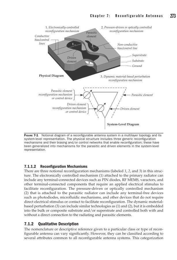
272 F r o n t i e r s i n a n t e n n a s : N e x t G e n e r a t i o n D e s i g n & e n g i n e e r i n g C h a p t e r 7 : r e c o n f i g u r a b l e a n t e n n a s 273
7.1.1.2 Reconfiguration MechanismsThere are three notional reconfiguration mechanisms (labeled 1, 2, and 3) in this struc-ture. The electronically controlled mechanism (1) attached to the primary radiator can include any terminal-connected devices such as PIN diodes, RF MEMS, varactors, and other terminal-connected components that require an applied electrical stimulus to facilitate reconfiguration. The pressure-driven or optically controlled mechanism (2) that is attached to the parasitic radiator can include any terminal-free devices such as photodiodes, microfluidic mechanisms, and other devices that do not require direct electrical stimulus or contact to facilitate reconfiguration. The dynamic material-based perturbation (3) can include similar technologies as (1) and (2), but it is embedded into the bulk or composite substrate and/or superstrate and controlled both with and without a direct connection to the radiating and parasitic elements.
7.1.2 Qualitative DescriptionThe nomenclature or descriptive reference given to a particular class or type of recon-figurable antenna can vary significantly. However, they can be classified according to several attributes common to all reconfigurable antenna systems. This categorization
Figure 7-1 Notional diagram of a reconfigurable antenna system in a multilayer topology and its system-level representation. The physical structure includes three generic reconfiguration mechanisms and their biasing and/or control networks that enable reconfiguration; these have been generalized into mechanisms for the parasitic and driven elements in the system-level representation.
1. Electronically-controlledreconfiguration mechanism
Conductivebias/control
lines Non-conductivebias/control line
Superstrate
Substrate
Ground
Drivenelement
Parasiticelement
Parasitic elementreconfiguration mechanism
or control device
Driven elementreconfiguration mechanism
or control deviceDriven element
Parasitic element
System-Level Diagram
Physical Diagram
3
21
2. Pressure-driven or optically controlledreconfiguration mechanism
3. Dynamic material-based perturbationreconfiguration mechanism

274 F r o n t i e r s i n a n t e n n a s : N e x t G e n e r a t i o n D e s i g n & e n g i n e e r i n g C h a p t e r 7 : r e c o n f i g u r a b l e a n t e n n a s 275
includes their reconfigurable performance metrics, the topology of the reconfigurable antenna system that facilitates this behavior, and the control or operation of the recon-figurable antenna system. The latter plays a critical role in the reconfigurable antenna system but does not typically appear in a description of the system so it is discussed later in this chapter.
The reconfigurable performance metrics can be consolidated into the two overarch-ing categories of radiation reconfigurable and frequency reconfigurable antennas. These two groupings are contextually broad given the scope of antenna parameters that each can encompass, but they provide a concise description of the reconfigurable performance. These two performance metrics are treated as mutually exclusive in this chapter for the purpose of describing the performance of the antenna, but the interdependence of these parameters with respect to the antenna’s behavior are closely linked. In the actual de-sign of the electromagnetically agile structure these parameters are coengineered to satisfy both parameters. However, the notion that one of these (radiation or frequency) is always fixed during the reconfiguration of the other depends on the intended appli-cation of the reconfigurable antenna. A brief, broad, and categorical description of these two follows to separate the performance metrics associated with their role in the recon-figurable antenna design.
7.1.2.1 Radiation ReconfigurableAntennas that can change any aspect of their radiation behavior while maintaining a stable matched impedance bandwidth are considered radiation reconfigurable antennas. This can encompass any far-field changes in the spatial properties of the radiated elec-tromagnetic fields and includes pattern shaping, polarization, phase, radar cross sec-tion, and nulls. The sample plots of radiation and frequency behavior shown in Fig. 7-2 illustrate these concepts for a radiation reconfigurable antenna with two spa-tially redirectional states (State 1 and State 2). For brevity, the full characterization of polarization and cut-plane information is not considered here. In this example both ra-diation configurations of the antenna operate over a common operating bandwidth or common impedance bandwidth that is shared in both states. This has been defined here by a target VSWR and target bandwidth with a center frequency f0. There are several examples presented in Section 7.3 that demonstrate this behavior.
Figure 7-2 Frequency (left) and radiation (right) behavior for a generic radiation reconfigurable antenna. The antenna has two reconfigurable states (1 and 2) with different radiation patterns that each operate within a target common impedance bandwidth.
Target
1Frequency Radiation patterns
State 1
Gmax
State 2Target
Commonimpedancebandwidth
f0
VSW
R
∞
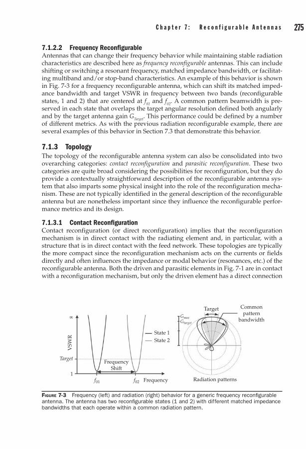
274 F r o n t i e r s i n a n t e n n a s : N e x t G e n e r a t i o n D e s i g n & e n g i n e e r i n g C h a p t e r 7 : r e c o n f i g u r a b l e a n t e n n a s 275
7.1.2.2 Frequency ReconfigurableAntennas that can change their frequency behavior while maintaining stable radiation characteristics are described here as frequency reconfigurable antennas. This can include shifting or switching a resonant frequency, matched impedance bandwidth, or facilitat-ing multiband and/or stop-band characteristics. An example of this behavior is shown in Fig. 7-3 for a frequency reconfigurable antenna, which can shift its matched imped-ance bandwidth and target VSWR in frequency between two bands (reconfigurable states, 1 and 2) that are centered at f01 and f02. A common pattern beamwidth is pre-served in each state that overlaps the target angular resolution defined both angularly and by the target antenna gain GTarget. This performance could be defined by a number of different metrics. As with the previous radiation reconfigurable example, there are several examples of this behavior in Section 7.3 that demonstrate this behavior.
7.1.3 TopologyThe topology of the reconfigurable antenna system can also be consolidated into two overarching categories: contact reconfiguration and parasitic reconfiguration. These two categories are quite broad considering the possibilities for reconfiguration, but they do provide a contextually straightforward description of the reconfigurable antenna sys-tem that also imparts some physical insight into the role of the reconfiguration mecha-nism. These are not typically identified in the general description of the reconfigurable antenna but are nonetheless important since they influence the reconfigurable perfor-mance metrics and its design.
7.1.3.1 Contact ReconfigurationContact reconfiguration (or direct reconfiguration) implies that the reconfiguration mechanism is in direct contact with the radiating element and, in particular, with a structure that is in direct contact with the feed network. These topologies are typically the more compact since the reconfiguration mechanism acts on the currents or fields directly and often influences the impedance or modal behavior (resonances, etc.) of the reconfigurable antenna. Both the driven and parasitic elements in Fig. 7-1 are in contact with a reconfiguration mechanism, but only the driven element has a direct connection
Figure 7-3 Frequency (left) and radiation (right) behavior for a generic frequency reconfigurable antenna. The antenna has two reconfigurable states (1 and 2) with different matched impedance bandwidths that each operate within a common radiation pattern.
Target
1Frequency
FrequencyShift
Radiation patterns
State 1
GmaxGtarget
State 2
Target Commonpattern
bandwidth
f01 f02
VSW
R
∞

276 F r o n t i e r s i n a n t e n n a s : N e x t G e n e r a t i o n D e s i g n & e n g i n e e r i n g C h a p t e r 7 : r e c o n f i g u r a b l e a n t e n n a s 277
that links the reconfiguration mechanism with the feed network; this distinction is often of practical importance.
7.1.3.2 Parasitic Reconfiguration The use of parasitic elements implies that the reconfiguration mechanism is not in di-rect contact with the radiating element. It is typically assumed that parasitic reconfigu-ration is performed by controlling the mutual coupling of discrete elements in the an-tenna structure. The resulting parasitic topologies are typically (but not always) less compact since they rely on a secondary element that is electromagnetically linked through its proximity to a driven element. These topologies are particularly useful in radiation reconfigurable antennas since the radiated energy can be steered or otherwise influenced to change its spatial characteristics without significantly impacting the tun-ing or the impedance behavior. The parasitic radiator in Fig. 7-1 illustrates how these systems could be utilized with reconfiguration mechanisms to alter the overall perfor-mance of the antenna.
7.2 AnalysisThe electromagnetic analysis of a reconfigurable antenna depends primarily on the type of antenna that is being manipulated and the antenna parameters that are desired. The analy-sis also depends greatly on the reconfiguration mechanism used to facilitate the desired changes and functionality. As with any antenna design the reconfigurable system should be described first by the physical topology (microstrip, waveguide, etc.) and its operation (resonant, leaky, etc.), preferably expressed using analytical techniques or methods that can impart physical insight into the operation of the design. Optimizers, numerical meth-ods, and commercially available field solvers are also power tools in this design process; these are especially helpful in the fine-tuning of a complex design. A truncated summary of analysis approaches is provided here only to highlight several of the basic electromag-netic concepts available to develop a physical understanding of these antennas. The reader is directed to other chapters of this book and standard references to obtain a rigorous mathematical analysis for a specific antenna design (e.g., [6]–[10]) and the electromagnetic theorems and concepts (e.g., [11]–[15]) that can be applied. In a general context, the analysis of a reconfigurable antenna system will require a blending of several analysis techniques to adequately model and predict the electromagnetic behavior.
7.2.1 Transmission Line, Network, and Circuit Models Analysis with transmission line and circuit equivalent models is typically the first step toward developing a physical understanding of a reconfigurable antenna design. The use of resonant and nonresonant line lengths, the extraction of equivalent RLC param-eters, and “black-box” networks provide straightforward insight into how physical changes will impact the performance of the antenna. These techniques are very com-mon when structures support a transverse electromagnetic (TEM) wave such as mi-crostrip, coplanar waveguide (CPW), and other printed antenna topologies. For the antenna in Fig. 7-1, one would begin by considering an equivalent model of the pri-mary radiator. The effect of the reconfiguration mechanism (1) could be captured in a black-box or circuit model and could be used in conjunction with the equivalent mi-crostrip transmission line structure created by the metalized areas. This approach could also be applied to gain a basic understanding of the parasitic element and reconfigura-tion mechanism (2), where an equivalent circuit could be used to model its inductive coupling to the driven element.

276 F r o n t i e r s i n a n t e n n a s : N e x t G e n e r a t i o n D e s i g n & e n g i n e e r i n g C h a p t e r 7 : r e c o n f i g u r a b l e a n t e n n a s 277
7.2.2 Perturbational TechniquesPerturbational techniques [11] are quite useful in the design and operation of reconfigu-rable antennas but require some a priori knowledge or accurate approximation of the antenna’s electromagnetic fields and radiating mechanisms. These methods are ex-tremely useful for calculating the effects of a constituent material or change to the sur-face of volumetric dimensions of the antenna. The analysis of the reconfiguration mech-anism (3) in Fig. 7-1 is ideally suited for these methods. For this mechanism the tuning of the primary radiator could be approximated by developing a cavity model for the calculation of resonant behavior and using material perturbation techniques to exam-ine the effect of altering the dielectric and/or magnetic properties of this disc-shaped material.
7.2.3 Variational Techniques Variational techniques are typically used to calculate characteristic quantities such as resonant frequency and input impedance. This differs from perturbational techniques since the variational procedure gives an approximate solution to the problem, while perturbational approaches provide changes to a known solution. These techniques are typically considered in more advanced designs where the amount of coupling to para-sitic elements and the determination of quantities in complex structures can be critical to the performance. An example of this would be to model the interaction between the primary and parasitic radiators in Fig. 7-1. In this case, the mutual coupling could be analyzed using arguments from reciprocity, but variational techniques could also be applied to the primary radiator to determine the approximate complex propagation constant used in the formation of the cavity model or to determine the resonant fre-quency as impacted by the parasitic radiator.
7.3 Overview of Reconfiguration Mechanisms for AntennasThe reconfiguration mechanism, or control device, represents one of the key consider-ations in the design of a reconfigurable antenna system. It is responsible for physically enabling the electromagnetic agility required to reconfigure the currents and fields on the antenna. The diversity of these mechanisms is equaled only by the reconfigurable anten-nas that they support. This section will address the use of these mechanisms by providing a summary of both mature and emerging reconfiguration technologies and their demon-strated usage in several antenna designs. These technologies have been organized into the four overarching categories of electromechanical, ferroic, solid state, and fluidic. Sev-eral examples have been taken from recent literature to illustrate each of these areas.
7.3.1 ElectromechanicalElectromechanical devices and systems can be very robust reconfiguration mechanisms and can facilitate many different operational modalities in a reconfigurable antenna. The application of mechanics into the design of reconfigurable antennas can be traced back to at least the early 1950s with the “cam and gear systems” developed for a trough wave-guide, or troughguide, antenna [16]. This system was developed as a traveling wave (leaky) antenna which provided fixed-frequency beamsteering by perturbing the fields to facilitate radiation and alter the propagation velocity for beamsteering. This reconfigurable radiation antenna used a variety of mechanically-driven mechanisms to perturb the propagating troughguide mode and enhance the leakage from its

278 F r o n t i e r s i n a n t e n n a s : N e x t G e n e r a t i o n D e s i g n & e n g i n e e r i n g C h a p t e r 7 : r e c o n f i g u r a b l e a n t e n n a s 279
open dimension. These systems were very well-conceived, included dynamic imped-ance matching, and performed well in their intended role as an electromechanically beamsteerable radar system. However, advancements in solid state switching and other phased-array technologies soon provided a more reliable and faster alternative to these mechanical systems. There have been significant and ongoing advances in micro- and nano-scale fabrication technologies since the first reported uses of the troughguide. Their reliability and proliferation have created new and even more viable opportunities for implementing mechanics into the design and operation of reconfigurable antennas (including new mechanisms for troughguide antenna systems [1]–[2]).
MEMS and nanoelectromechanical systems (NEMS) now provide the basis for many of the unique electromechanical reconfiguration technologies. The term radio fre-quency in RF MEMS and RF NEMS emphasizes their specific design for use in high frequency applications where loss mechanisms, electrical dimension, and wave imped-ance or propagation are critical. The small size of these electromechanical systems pro-vides antenna engineers with the truly unique opportunity to incorporate switching and loading mechanisms in a packaged configuration or as a mechanism that can be fabricated in situ or onto the antenna. The small size helps to avoid unwanted transmis-sion-line effects or loading within the device and can be used to create structurally recon-figurable antenna systems where the moving parts are structural elements of the design. However, there are other electromechanical means and material systems that can also be used to this end.
MEMS, NEMS, and other electromechanical mechanisms are often interfaced through wire bonds and other interconnects, or terminals, for biasing, control, and elec-tromagnetic functionality. Provided these terminals are sufficiently isolated by way of the package and electromechanical design, this topology makes them ideally suited for switching, routing, and other duties in the RF front-end chain where electrically con-ductive bias and control lines can be efficiently navigated to and around the terminals in a multilayer environment. Isolating the antenna’s virtual terminals for radiated modes and the near-fields of the antenna’s radiating mechanism creates additional integration challenges. If their isolation from bias and control structures is not sufficient, there is a potential for them to interfere with the intended operation of the antenna through spurious radiation or reactive loading. As a result, many of the designs using these devices have developed careful and clever means to create the required conditions for isolation. This important artifact of terminal-driven devices also applies to many of the solid state and ferroic reconfiguration mechanisms discussed in Sections 7.1.2 and 7.1.3, respectively.
7.3.1.1 Packaged RF MEMS and RF NEMS Packaged RF MEMS and RF NEMS can be utilized in reconfigurable antenna designs as switching mechanisms and tunable discrete elements such as variable inductors and varactors [5]. The MEMS and related micro- or nano-scale components are often her-metically sealed, or packaged, in these structures. This protects the movable parts from exposure to environmental parameters such as moisture and dust. It also provides physical protection from damage during handling or normal operation. The packaged unit also enables its integration into platforms using rapid pick-and-place methods for mass fabrication and assembly. Two examples are discussed here to illustrate some of the key considerations that go into the design of a reconfigurable antenna enabled by packaged RF MEMS switches.

278 F r o n t i e r s i n a n t e n n a s : N e x t G e n e r a t i o n D e s i g n & e n g i n e e r i n g C h a p t e r 7 : r e c o n f i g u r a b l e a n t e n n a s 279
The first example is the reconfigurable radiation single turn spiral antenna [17] shown on the left side of Fig. 7-4. This antenna uses two RadantTM RF MEMS single-pull single-throw (SPST) switches [18] to achieve two reconfigurable states. The fabricated antenna and radiation patterns for both configurations are shown in the left and right of Fig. 7-5, respectively. An impedance tuning stub, two back-to-back quarter-wavelength short cir-cuit bias stubs, and two quarter-wavelength short-circuit control lines with lumped-ele-ment bias tees (through a capacitor to ground and bias resistor to a control voltage) were used to achieve the desired antenna performance. The equivalent transmission line models
Figure 7-4 CAD model of the radiation reconfigurable antenna using two packaged RF MEMS switches (left) and equivalent transmission line model of the bias, control, and stub matching network (right) (Huff et al. [17], © IEEE 2006)
Line segment 3
Line segment 1
Line segment 2
Switch #2
Switch #1
Tuning stub
g2
g1
d2d1
s2
s1
Antenna BiasNetwork
Via to ground(short circuit) Via to ground
(short circuit)DC source
Switch
B
Switch 2
Switch 1
Open circuit stubSingle stubmatchingnetwork
Gate biasnetwork
Shared via to ground(short circuit)
βA, ZA βs, Zs
βS, ZS
βA, ZA βA, ZA βA, ZA
βA, ZA
βM, ZM
βB, ZBβB, ZBβB, ZB
IM
1 pF
V
100 kΩλeff
4
λeff
4
λeff
4
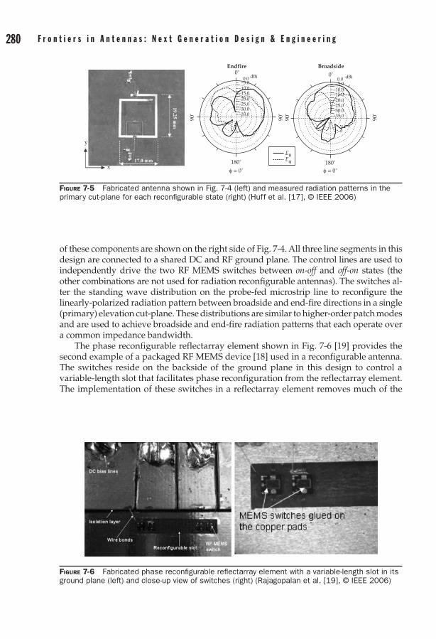
280 F r o n t i e r s i n a n t e n n a s : N e x t G e n e r a t i o n D e s i g n & e n g i n e e r i n g C h a p t e r 7 : r e c o n f i g u r a b l e a n t e n n a s 281
of these components are shown on the right side of Fig. 7-4. All three line segments in this design are connected to a shared DC and RF ground plane. The control lines are used to independently drive the two RF MEMS switches between on-off and off-on states (the other combinations are not used for radiation reconfigurable antennas). The switches al-ter the standing wave distribution on the probe-fed microstrip line to reconfigure the linearly-polarized radiation pattern between broadside and end-fire directions in a single (primary) elevation cut-plane. These distributions are similar to higher-order patch modes and are used to achieve broadside and end-fire radiation patterns that each operate over a common impedance bandwidth.
The phase reconfigurable reflectarray element shown in Fig. 7-6 [19] provides the second example of a packaged RF MEMS device [18] used in a reconfigurable antenna. The switches reside on the backside of the ground plane in this design to control a variable-length slot that facilitates phase reconfiguration from the reflectarray element. The implementation of these switches in a reflectarray element removes much of the
Figure 7-6 Fabricated phase reconfigurable reflectarray element with a variable-length slot in its ground plane (left) and close-up view of switches (right) (Rajagopalan et al. [19], © IEEE 2006)
Figure 7-5 Fabricated antenna shown in Fig. 7-4 (left) and measured radiation patterns in the primary cut-plane for each reconfigurable state (right) (Huff et al. [17], © IEEE 2006)
Endfire Broadside0˚ 0˚
180˚
EθEφ
φ = 0˚ φ = 0˚180˚
90˚
90˚
90˚
90˚
0.0 dBi–5.0
–10.0–15.0–20.0–25.0–30.0–35.0
0.0 dBi–5.0
–10.0–15.0–20.0–25.0–30.0–35.0
x
y

280 F r o n t i e r s i n a n t e n n a s : N e x t G e n e r a t i o n D e s i g n & e n g i n e e r i n g C h a p t e r 7 : r e c o n f i g u r a b l e a n t e n n a s 281
sensitivity to biasing and control structures that were present in the previous example [17]. Operationally, the RF MEMS switches are placed across the slot and its length is changed by turning the switches on and off. This effectively places shorts across the slot at the four switch locations to create sixteen discrete reconfigurable states (several are operationally identical due to symmetry). The presence of this slot below the patch provides an inductive loading to the reflectarray element. This loading introduces a phase shift in the re-radiated signal. The phase of the reflected field from each reflectar-ray element can be changed by determining the location of the RF MEMS switches. This configuration provides a very amendable integration environment for the switch since the radiating patch elements can be printed on the top layer and a slot of fixed length can be cut in the ground plane of each element. Several of the switch configurations and their measured phase from a waveguide experiment are shown on the left and right side of Fig. 7-7, respectively.
7.3.1.2 In situ Fabricated RF MEMS Microelectromechanical systems fabricated onto or within the antenna structure pro-vide a more direct method for the integration of reconfiguration mechanisms into the antenna design. These switching and reactive loading mechanisms are typically subwavelength in size and very similar in operation to their packaged counterparts. This approach can include the cofabrication of antenna and reconfiguration mechanisms or the fabrication of reconfiguration mechanisms onto an existing antenna structure. The fabrication of these devices directly onto the antenna can mitigate some of the undesired interaction with packaging or hermetic sealing and loading from wire bonding. However, many of the challenges in providing biasing and control to the reconfiguration mecha-nism are still present. The ability to provide biasing directly through the structure in a nonterminal configuration creates many opportunities. Four examples are presented to illustrate the design and integration of RF MEMS and NEMS reconfiguration mecha-nisms directly onto the antenna and provide an overview of the different bias and control schemes that can be used to enable their operation.
Figure 7-8 shows the topside and bottom of a frequency reconfigurable annular slot antenna [20], which uses two different kinds of electrostatically-actuated suspended-membrane (cantilever-type) MEMS as reconfiguration mechanisms. The base antenna design consists of two concentric circular slots that can be independently excited to re-configure the operational frequency. Independent excitation is achieved using a single-arm cantilever-type MEMS actuator to create a variable-length microstrip feed line on
Figure 7-7 Switch configurations and their measured phase from a waveguide fabricated antenna shown in Fig. 7-4 (left) and measured radiation patterns in the primary cut-plane for each reconfig-urable state (right) (Rajagopalan et al. [19], © IEEE 2006)
State 9
State 15 State 41 1 1 1 10 0 0
State 1
Symmetric loading Asymmetric loading
– Switch OFF (0)
40
0
–40
–80
–120
–1600 2 4 6 8 10 12
Number of quantized steps
Ref
lect
ion
phas
e (d
eg)
Measurement Simulation
@ 2 GHz0
1.89
2.43.12
11.135.10
67.14
15
– Switch ON (1)
Effective slot length Effective slot length
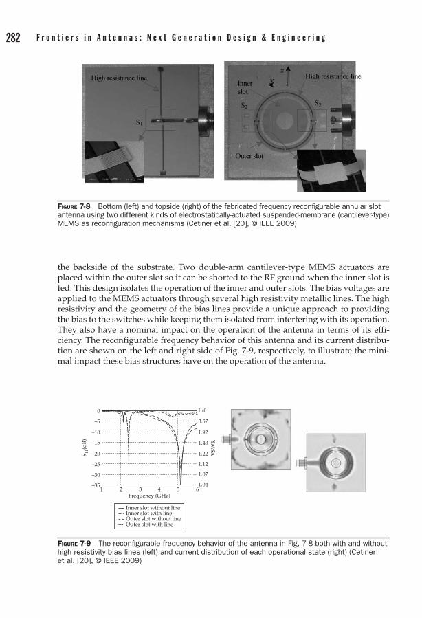
282 F r o n t i e r s i n a n t e n n a s : N e x t G e n e r a t i o n D e s i g n & e n g i n e e r i n g C h a p t e r 7 : r e c o n f i g u r a b l e a n t e n n a s 283
the backside of the substrate. Two double-arm cantilever-type MEMS actuators are placed within the outer slot so it can be shorted to the RF ground when the inner slot is fed. This design isolates the operation of the inner and outer slots. The bias voltages are applied to the MEMS actuators through several high resistivity metallic lines. The high resistivity and the geometry of the bias lines provide a unique approach to providing the bias to the switches while keeping them isolated from interfering with its operation. They also have a nominal impact on the operation of the antenna in terms of its effi-ciency. The reconfigurable frequency behavior of this antenna and its current distribu-tion are shown on the left and right side of Fig. 7-9, respectively, to illustrate the mini-mal impact these bias structures have on the operation of the antenna.
Figure 7-8 Bottom (left) and topside (right) of the fabricated frequency reconfigurable annular slot antenna using two different kinds of electrostatically-actuated suspended-membrane (cantilever-type) MEMS as reconfiguration mechanisms (Cetiner et al. [20], © IEEE 2009)
Figure 7-9 The reconfigurable frequency behavior of the antenna in Fig. 7-8 both with and without high resistivity bias lines (left) and current distribution of each operational state (right) (Cetiner et al. [20], © IEEE 2009)
0
–5
–10
–15
–20
–25
–30
–351 2 3 4
Frequency (GHz)
VSW
R
S 11(d
B)
5 6
Inf
3.57
1.92
1.43
1.22
1.12
1.07
1.04
Inner slot without line
Outer slot without lineInner slot with line
Outer slot with line

282 F r o n t i e r s i n a n t e n n a s : N e x t G e n e r a t i o n D e s i g n & e n g i n e e r i n g C h a p t e r 7 : r e c o n f i g u r a b l e a n t e n n a s 283
The frequency reconfigurable Sierpinski antenna [21] in Fig. 7-10 and Fig. 7-11 illustrates the use of MEMS switches that have been designed to operate with varying actuation voltages. In this device, the single DC bias voltage and the RF signal are ap-plied to both the antenna and switches through the center conductor of the coplanar waveguide (CPW) feed line. Reconfigurability is achieved through the placement of switches with actuation voltages applied to the antenna structure that increase in succession as they are placed farther away from the feed. Figure 7-10 shows the basic
Figure 7-10 Sequentially reconfigurable Sierpinski antenna (left) and its four operational states enabled by RF MEMS switches with varying DC bias voltages (Kingsley et al., [21], © IEEE/ASME 2007)
Figure 7-11 The frequency reconfigurable antenna fabricated on a flexible organic substrate (left) and measured results (right) for the four states that operate at different bias voltages (Kingsley et al. [21], © IEEE/ASME 2007)
0
–5
–10
–15
–20
–25
–30
–355 10 15 20 25
Frequency (GHz)11 mm
Switch 1 Switch 2 Switch 3 Switch 4
6 mm
20 mm
25 mmS2
S1
S3
S1’
S2’
S3’
60º
x
y
z
S 11 (d
B)
State 1State 2State 3State 4
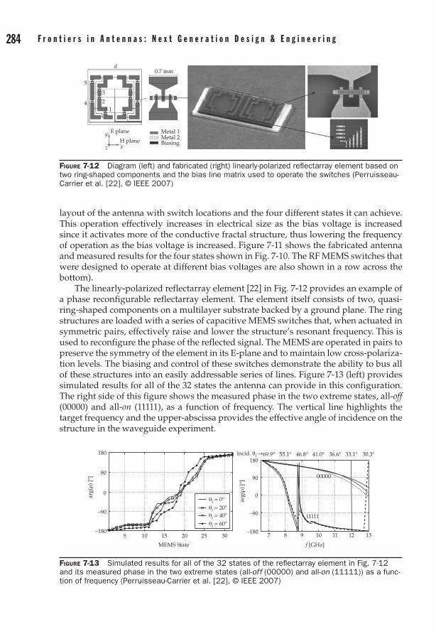
284 F r o n t i e r s i n a n t e n n a s : N e x t G e n e r a t i o n D e s i g n & e n g i n e e r i n g C h a p t e r 7 : r e c o n f i g u r a b l e a n t e n n a s 285
layout of the antenna with switch locations and the four different states it can achieve. This operation effectively increases in electrical size as the bias voltage is increased since it activates more of the conductive fractal structure, thus lowering the frequency of operation as the bias voltage is increased. Figure 7-11 shows the fabricated antenna and measured results for the four states shown in Fig. 7-10. The RF MEMS switches that were designed to operate at different bias voltages are also shown in a row across the bottom).
The linearly-polarized reflectarray element [22] in Fig. 7-12 provides an example of a phase reconfigurable reflectarray element. The element itself consists of two, quasi-ring-shaped components on a multilayer substrate backed by a ground plane. The ring structures are loaded with a series of capacitive MEMS switches that, when actuated in symmetric pairs, effectively raise and lower the structure’s resonant frequency. This is used to reconfigure the phase of the reflected signal. The MEMS are operated in pairs to preserve the symmetry of the element in its E-plane and to maintain low cross-polariza-tion levels. The biasing and control of these switches demonstrate the ability to bus all of these structures into an easily addressable series of lines. Figure 7-13 (left) provides simulated results for all of the 32 states the antenna can provide in this configuration. The right side of this figure shows the measured phase in the two extreme states, all-off (00000) and all-on (11111), as a function of frequency. The vertical line highlights the target frequency and the upper-abscissa provides the effective angle of incidence on the structure in the waveguide experiment.
Figure 7-12 Diagram (left) and fabricated (right) linearly-polarized reflectarray element based on two ring-shaped components and the bias line matrix used to operate the switches (Perruisseau-Carrier et al. [22], © IEEE 2007)
0.7 mm
Metal 1Metal 2Biasing
4 2
3
1
E plane
H planex
y
z
5
d
Figure 7-13 Simulated results for all of the 32 states of the reflectarray element in Fig. 7-12 and its measured phase in the two extreme states (all-off (00000) and all-on (11111)) as a func-tion of frequency (Perruisseau-Carrier et al. [22], © IEEE 2007)
180
90
0
–90
–1805 10 15 20 25 30
MEMS State
arg(ρ)
[º]
θi = 60ºθi = 40ºθi = 20ºθi = 0º
180
90
0
–90
–180 7 8 9 10
f [GHz]
11 12 13
arg(ρ)
[º]
incid. θiÆ69.9° 55.1° 46.8° 41.0° 36.6° 33.1° 30.3°
00000
11111

284 F r o n t i e r s i n a n t e n n a s : N e x t G e n e r a t i o n D e s i g n & e n g i n e e r i n g C h a p t e r 7 : r e c o n f i g u r a b l e a n t e n n a s 285
The tunable optical bowtie antenna [23] in Fig. 7-14 consists of two self-aligned identi-cal triangular structures with their nano-scale tips coated in metal. These structures create the termination for two in-plane movable cantilevers that are connected to and supported by bentbeam electrothermal actuators. The in-plane movement of the apex of the bent-beams alters the gap distance between the two tips of the bowtie antenna which effec-tively lengthens the nanoantenna and lowers its frequency response. The bowtie diagram and optical response of the structure are shown in Fig. 7-15 to illustrate the basic behavior of the reconfigurable system. This effect is subject to the plasmonic behavior of the metal-ized areas, which can create other loading on the structure (based on metal thickness, etc.) but follows from classical antenna theory. The actual reconfiguration of the antenna is simplistic, but the use of nanoscale antenna concepts demonstrates the evolution of recon-figurable antenna design into the optical range of the frequency spectrum.
7.3.1.3 Structurally Reconfigurable Electromechanical SystemsThe category of electromechanical mechanisms for structurally reconfigurable anten-nas and radiating systems encompasses a very wide range of technologies. This in-cludes antennas based on MEMS and NEMS mechanisms such as the micromachined Vee antenna [24], but it also incorporates many other methods of reconfiguration. Material-based techniques using electroactive and shape-memory materials provide an emerging approach and unique alternative to electromechanical reconfiguration mechanisms driven by the electrostatic actuation of metallic elements. These electro-active materials have been studied for some time and recently have been of interest in
Figure 7-14 The CAD (left) and SEM image (right) of the tunable optical bowtie antenna using two self-aligned identical triangular structures with their nano-scale tips coated in metal (Penmetsa et al., [23], © IEEE 2009)
Electrode
MEMSplatform
MEMSplatform
Movable direction
Antenna
Nanoantenna
Bow-tieantenna
75X 200 µm
Figure 7-15 Bowtie diagram (left) and normalized optical intensity of the tunable optical bowtie antenna using different gap distances (right) (Penmetsa et al., [23], © IEEE 2009)
Light polarization
h g g
h
θ
Metal (Au) Dielectric Air
1
0.8
0.6
0.4
0.2
0
1
0.8
0.6
0.4
0.2
01000 1500 2000 600 650 700 750 800
Wavelength (nm) Wavelength (nm)
Nor
mal
ized
Inte
nsit
y
Nor
mal
ized
Inte
nsit
y
(a) (b)
g = 30 nm g = 30 nmg = 60 nm g = 60 nmg = 120 nm g = 120 nm
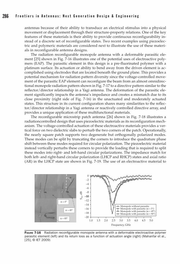
286 F r o n t i e r s i n a n t e n n a s : N e x t G e n e r a t i o n D e s i g n & e n g i n e e r i n g C h a p t e r 7 : r e c o n f i g u r a b l e a n t e n n a s 287
antennas because of their ability to transduce an electrical stimulus into a physical movement or displacement through their structure-property relations. One of the key features of these materials is their ability to provide continuous reconfigurability in-stead of a discrete set of reconfigurable states. Two recent examples using piezoelec-tric and polymeric materials are considered next to illustrate the use of these materi-als in reconfigurable antenna designs.
The radiation reconfigurable monopole antenna with a deformable parasitic ele-ment [25] shown in Fig. 7-16 illustrates one of the potential uses of electroactive poly-mers (EAP). The parasitic element in this design is a pre-fluorinated polymer with a platinum surface. Its actuation or ability to bend away from the driven element is ac-complished using electrodes that are located beneath the ground plane. This provides a potential mechanism for radiation pattern diversity since the voltage-controlled move-ment of the parasitic EAP element can reconfigure the beam from an almost omnidirec-tional monopole radiation pattern shown in Fig. 7-17 to a directive pattern similar to the reflector/director relationship in a Yagi antenna. The deformation of the parasitic ele-ment significantly impacts the antenna’s impedance and creates a mismatch due to its close proximity (right side of Fig. 7-16) in the unactuated and moderately actuated states. This structure in its current configuration shares many similarities to the reflec-tor/director relationship in a Yagi antenna or reactively controlled directive array, and provides a unique application of these multifunctional materials.
The reconfigurable microstrip patch antenna [26] shown in Fig. 7-18 illustrates a radiationcontrolled design that uses piezoelectric materials as its reconfiguration mech-anism. The voltage-controlled actuation of these electroactive materials provides a ver-tical force on two dielectric slabs to perturb the two corners of the patch. Operationally, the nearly square patch supports two degenerate but orthogonally polarized modes. These modes can be split by truncating the corners to introduce the quadrature phase shift between these modes required for circular polarization. The piezoelectric material instead vertically perturbs these corners to provide the loading that is required to split these modes into right- and left-hand circular polarizations. The impedance match for both left- and right-hand circular polarization (LHCP and RHCP) states and axial ratio (AR) in the LHCP state are shown in Fig. 7-19. The use of an electroactive material to
Figure 7-16 Radiation reconfigurable monopole antenna with a deformable electroactive polymer parasitic element (left) and its return loss as a function of actuation angle (right) (Mahanfar et al., [25], © IET 2009)
0–2
–4–6
–8
–10–10
–12
–14
–16
–18
–201.0 1.5 2.0 2.5 3.0
Frequency, GHz
3.5 4.0 4.5 5.0
S 11,
dB
Monopole without parasiticMonopole with parasitic (α = 5°)
α = 0°
α
α = 45°
α = 85°
Monopole with parasitic (α = 45°)Monopole with parasitic (α = 90°)
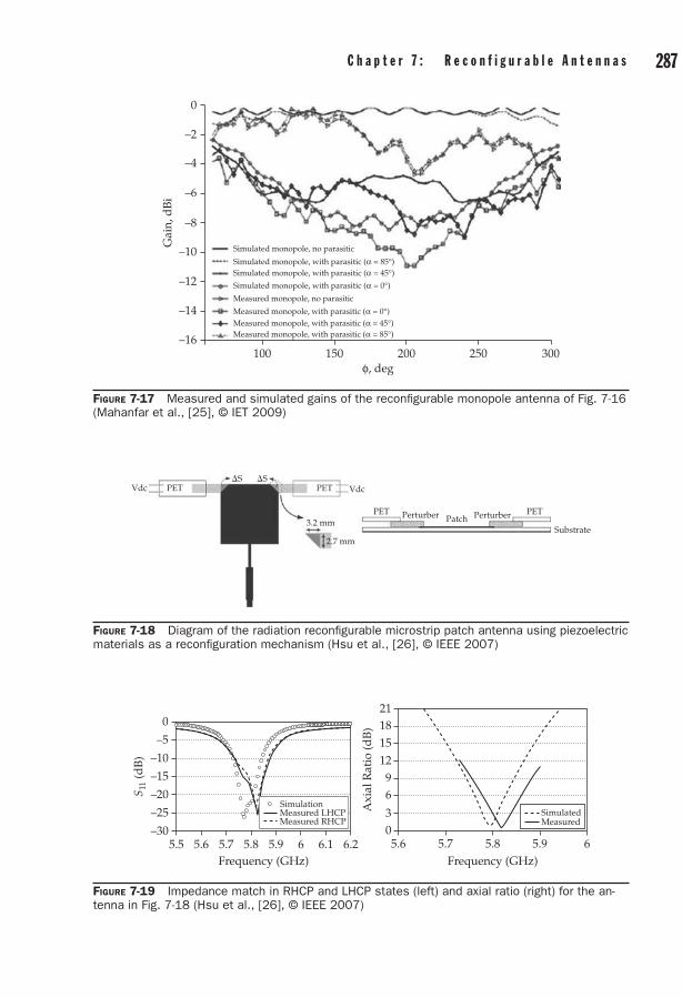
286 F r o n t i e r s i n a n t e n n a s : N e x t G e n e r a t i o n D e s i g n & e n g i n e e r i n g C h a p t e r 7 : r e c o n f i g u r a b l e a n t e n n a s 287
Figure 7-17 Measured and simulated gains of the reconfigurable monopole antenna of Fig. 7-16 (Mahanfar et al., [25], © IET 2009)
0
–2
–4
–6
–8
–10
–12
–14
–16100 150
φ, deg200 250 300
Gai
n, d
Bi
Simulated monopole, no parasitic
Measured monopole, no parasitic
Measured monopole, with parasitic (α = 0°)Measured monopole, with parasitic (α = 45°)Measured monopole, with parasitic (α = 85°)
Simulated monopole, with parasitic (α = 85°)Simulated monopole, with parasitic (α = 45°)
Simulated monopole, with parasitic (α = 0°)
Figure 7-18 Diagram of the radiation reconfigurable microstrip patch antenna using piezoelectric materials as a reconfiguration mechanism (Hsu et al., [26], © IEEE 2007)
Vdc VdcPETDS DS
PET
PET PET3.2 mm
2.7 mm
Perturber PerturberPatchSubstrate
Figure 7-19 Impedance match in RHCP and LHCP states (left) and axial ratio (right) for the an-tenna in Fig. 7-18 (Hsu et al., [26], © IEEE 2007)
Axi
al R
atio
(dB
)
5.6 5.7 5.8 5.9 6
SimulationMeasured LHCPMeasured RHCP
–5
0
–10
–15
–20
–25
–30
S 11
(dB
)
5.5 5.6 5.7 5.8 5.9 6 6.1 6.2Frequency (GHz) Frequency (GHz)
2118151296
30
MeasuredSimulated
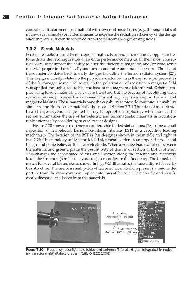
288 F r o n t i e r s i n a n t e n n a s : N e x t G e n e r a t i o n D e s i g n & e n g i n e e r i n g C h a p t e r 7 : r e c o n f i g u r a b l e a n t e n n a s 289
control the displacement of a material with lower intrinsic losses (e.g., the small slabs of microwave laminate) provides a means to increase the radiation efficiency of the design since they are sufficiently removed from the performance-governing fields.
7.3.2 Ferroic MaterialsFerroic (ferroelectric and ferromagnetic) materials provide many unique opportunities to facilitate the reconfiguration of antenna performance metrics. In their most concep-tual form, they impart the ability to alter the dielectric, magnetic, and/or conductive material properties both locally and across an entire antenna or aperture. The use of these materials dates back to early designs including the ferrod radiator system [27]. This design is closely related to the polyrod radiator but uses the anisotropic properties of the ferromagnetic material to switch the polarization of radiation: a magnetic field was applied through a coil to bias the base of the magneto-dielectric rod. Other exam-ples using ferroic materials also exist in literature, but the process of negotiating these material property changes has remained constant (e.g., applying electric, thermal, and magnetic biasing). These materials have the capability to provide continuous tunability similar to the electroactive materials discussed in Section 7.3.1.3 but do not make struc-tural changes beyond changes to their crystallographic morphology when biased. This section summarizes the use of ferroelectric and ferromagnetic materials in reconfigu-rable antennas by considering several recent designs.
Figure 7-20 shows a frequency reconfigurable folded slot antenna [28] using a small deposition of ferroelectric Barium Strontium Titanate (BST) as a capacitive loading mechanism. The location of the BST in this design is shown in the middle and right of Fig. 7-20. This topology utilizes the folded-slot metallization as an upper electrode and the ground plane below as the lower electrode. When a voltage bias is applied between the antenna and ground plane the permittivity of this small section of BST is altered. This changes the capacitance of this small section along the antenna and reactively loads the structure (similar to a varactor) to reconfigure the frequency. The impedance match for several biased states shown in Fig. 7-21 illustrates the tunability achieved by this structure. The use of a small patch of ferroelectric material represents a unique de-parture from the more common implementations of ferroelectric materials and signifi-cantly decreases the losses from the materials.
Figure 7-20 Frequency reconfigurable folded-slot antenna (left) utilizing an integrated ferroelec-tric varactor (right) (Palukuru et al., [28], © IEEE 2008)
FSA BST varactor
Upper silverelectrode (t ~ 10 µm)
BST (t ~ 25 µm)AluminaGround plane
200 µm
FSABST
Varactor
Alumina Groundplane

288 F r o n t i e r s i n a n t e n n a s : N e x t G e n e r a t i o n D e s i g n & e n g i n e e r i n g C h a p t e r 7 : r e c o n f i g u r a b l e a n t e n n a s 289
The cross-sectional diagram of the ferrite-filled slotted rectangular waveguide [29] in Fig. 7-22 illustrates the use of ferromagnetic materials in the design of reconfigurable antennas. The structure is transversely magnetized to alter the phase velocity of the propagating wave. This alters the phase distribution across the slotted structure to achieve the main beamsteering characteristics shown on the left side of Fig. 7-22. This structure resembles many of the reconfigurable antennas based on corrugated struc-tures [2] but makes careful consideration to avoid the ferromagnetic resonance where losses dominate the properties of the ferromagnetic material. A more optimal use of the materials could be conceptualized as the previous example of ferroelectric materials, but the magnetic bias field provides difficulties in providing this in a convenient loca-tion that does not interact with the performance of the antenna. The fabricated antenna assembly (including matching networks) is shown in Fig. 7-23 along with its radiation behavior (beamsteering for two different biases).
Figure 7-21 Impedance match of the reconfigurable folded slot antenna utilizing an integrated ferroelectric varactor (Palukuru et al., [28], © IEEE 2008)
0
–10
–20
–30
–40
Ret
urn
Los
s [d
B]
2.5 3.53.0 4.54.0
Frequency [GHz]
3.18 3.25
3.73
3.29
Reference antenna5.6 V/µm (Vbias = 200 V)
2.9 V/µm (Vbias = 100 V)
0 V/µm (Vbias = 0 V)
Figure 7-22 Cross-sectional diagram of the ferrite-filled slotted rectangular waveguide (left) and beamsteering characteristics as a function of bias field and different ferromagnetic thicknesses (right) (Palukuru et al., [29], © IEEE 2008)
PEC
... ...
xi
b1
–a – lT –a a
θs
a+lT
b4
b
d
z
xy
(II)
Incident wave
Hin
Region (I)
Region (III)
50
30
10
–10
–30
–500 400 800 1200 1600 2000
Mai
n be
am d
irec
tion
(deg
)
Applied magnetic bias Hin (oe)
Region (IV): ferrite slab
b1 = 0.0 mm, b4= 6.7 mmb1 = 1.5 mm, b4= 5.2 mmb1 = 3.0 mm, b4= 3.7 mm
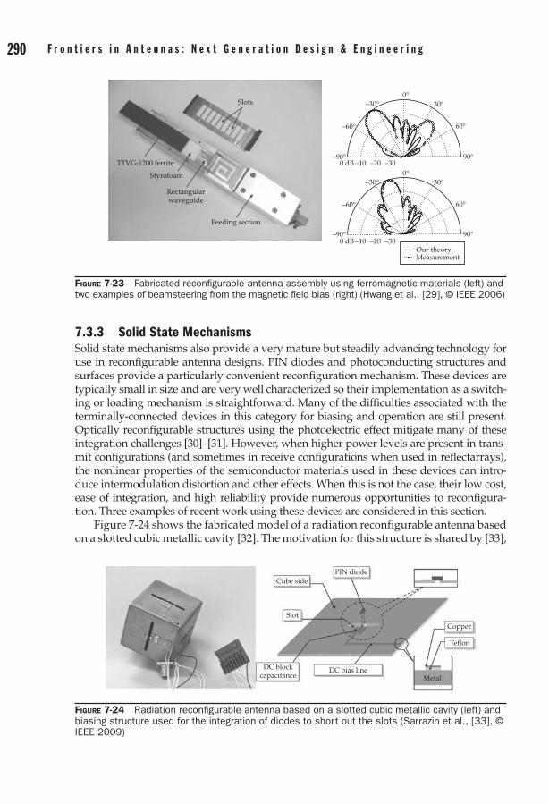
290 F r o n t i e r s i n a n t e n n a s : N e x t G e n e r a t i o n D e s i g n & e n g i n e e r i n g C h a p t e r 7 : r e c o n f i g u r a b l e a n t e n n a s 291
7.3.3 Solid State MechanismsSolid state mechanisms also provide a very mature but steadily advancing technology for use in reconfigurable antenna designs. PIN diodes and photoconducting structures and surfaces provide a particularly convenient reconfiguration mechanism. These devices are typically small in size and are very well characterized so their implementation as a switch-ing or loading mechanism is straightforward. Many of the difficulties associated with the terminally-connected devices in this category for biasing and operation are still present. Optically reconfigurable structures using the photoelectric effect mitigate many of these integration challenges [30]–[31]. However, when higher power levels are present in trans-mit configurations (and sometimes in receive configurations when used in reflectarrays), the nonlinear properties of the semiconductor materials used in these devices can intro-duce intermodulation distortion and other effects. When this is not the case, their low cost, ease of integration, and high reliability provide numerous opportunities to reconfigura-tion. Three examples of recent work using these devices are considered in this section.
Figure 7-24 shows the fabricated model of a radiation reconfigurable antenna based on a slotted cubic metallic cavity [32]. The motivation for this structure is shared by [33],
Figure 7-23 Fabricated reconfigurable antenna assembly using ferromagnetic materials (left) and two examples of beamsteering from the magnetic field bias (right) (Hwang et al., [29], © IEEE 2006)
–90°
–60°
–30°0°
30°
60°
90°0 dB –10 –20 –30
–90°
–60°
–30°0°
30°
60°
90°0 dB –10 –20 –30
Slots
TTVG-1200 ferrite
Styrofoam
Rectangularwaveguide
Feeding section
Our theoryMeasurement
Figure 7-24 Radiation reconfigurable antenna based on a slotted cubic metallic cavity (left) and biasing structure used for the integration of diodes to short out the slots (Sarrazin et al., [33], © IEEE 2009)
Cube sidePIN diode
Slot
DC blockcapacitance
DC bias lineMetal
Copper
Teflon

290 F r o n t i e r s i n a n t e n n a s : N e x t G e n e r a t i o n D e s i g n & e n g i n e e r i n g C h a p t e r 7 : r e c o n f i g u r a b l e a n t e n n a s 291
but fed by a single probe through one corner of the cubic structure instead of using four independently-fed radiation reconfigurable antennas. The insertion length of the probe provides a means to simultaneously excite the three orthogonal cavity modes or the slots themselves. The linearly polarized slots are placed along all six of the cube sides to enable the radiation. Each adjacent slot is orthogonal so the total radiated fields are the sum of three orthogonal polarizations for every given direction of propagation. Pattern reconfiguration is achieved by PIN diode switches that are placed along the middle of each slot. Hence, in the on state the switches act as shortcircuits and disable the radia-tion from these slots, and in the off state the radiation from slots can occur. The right side of Fig. 7-24 shows a very innovative method for biasing the diode while keeping its DC bias isolated from the cube. A thin dielectric sheet of Teflon inserted between the diode and the metallic cube sides creates a capacitance under one of the diode pins and allows the transmission of RF signals while stopping DC potentials. The measured perfor-mance of these three configurations is shown in Fig. 7-25. When the antenna is verti-cally oriented along the axis of the probe, this configuration contains two short-circuited slots on the lower sides and one on the upper side. This is equivalent to mechanically rotating the cube around the probe in three equal increments. The resulting envelope correlation coefficient as a function of cross-polar discrimination (XPD) is also shown in Fig. 7-25 to illustrate the diversity of the patterns in the three configurations.
The CPW-fed slot bowtie antenna [34] shown in Fig. 7-26 is another example of a frequency reconfigurable design using PIN diodes. This structure achieves frequency agility by introducing band-reject capabilities into an inherently wideband structure. Frequency rejection is accomplished in this design through a series of symmetric slots that are integrated into one arm of the bowtie structure to create a high-impedance transmission line structure, which acts as a filtering mechanism within the antenna (Fig. 7-26). The total length of these slots ultimately determines their stop-band fre-quency. The PIN diodes are placed along the slot to activate the desired stop-band
Figure 7-25 Measured impedance match (left) and envelope correlation coefficient (right) for three configurations that effectively provide an equiangular rotation of the structure about the axis of the probe feed (Sarrazin et al., [33], © IEEE 2009)
–10 dB sharedbandwidth
Configuration 1, ∆f = 8.8%Configuration 2, ∆f = 5.4%Configuration 3, ∆f = 6.8%
5
0
–5
–10
–15
–20
–254.5 4.6 4.7 4.8 4.9 5 5.1 5.2 5.3 5.4 5.5 5.6 5.7 5.8 5.9 6 –20 –15 –10 –5 0 5 10 15 20
S 11 (d
B)
Frequency (GHz)
ρ e
ρe12 :measurementρe13 :measurementρe23 :measurementρe :simulationρe :simulation with PIN diodes
0.5
0.45
0.4
0.35
0.3
0.25
0.2
0.15
0.1
0.05
0
XPD (dB)

292 F r o n t i e r s i n a n t e n n a s : N e x t G e n e r a t i o n D e s i g n & e n g i n e e r i n g C h a p t e r 7 : r e c o n f i g u r a b l e a n t e n n a s 293
characteristics by effectively changing the length of the line. The number of PIN diode pairs (which are used for symmetry) and their positions ultimately determine the number and location of the available rejection frequencies. The impedance match and peak gain from several configurations are shown in Fig. 7-27. These illustrate the effec-tiveness and losses associated with the integration of the diodes onto the wideband structure.
Historically, the primary application of photonic or optical technologies for antenna systems has been on the development of RF link and beamsteering techniques. How-ever, over the last two decades, there has been a focus on using photonic techniques for antenna reconfiguration [30]. By using photonically controlled devices (switches, reac-tive devices, and photoconductive materials) it is possible to produce both radiation and frequency reconfiguration. Photonically controlled devices do not require conduct-ing lines to provide power, control, or bias signals but instead use fiber optical cables or direct optical illumination to control the device or to manifest changes in the materials. Optical fibers do not perturb the antenna fields significantly, since they are made of low
Figure 7-26 Frequency reconfigurable CPW-fed slot bowtie antenna, which uses switched PIN di-odes for control (J. Perruisseau-Carrier et al., [34], © IEEE 2010)
A ACB BC
PINdiode
DCReturn path
Couplingcapacitors
Biaswires
C B APIN diodes
DClines
Via
d1d2
d3 222
11
11
Figure 7-27 Frequency reconfigurable CPW-fed slot bowtie antenna, which uses switched PIN di-odes for control. Return loss is plotted on the left and peak realized gain is plotted on the right (J. Perruisseau-Carrier et al., [34], ©IEEE 2010)
0
–4
ABC
–8
–12
–16
–201.5 2.5 3.5 4.5 52 3
Frequency [GHz]4 1.5 2.5 3.5 4.5 52 3
Frequency [GHz]
Peak
Rea
lized
Gai
n [d
Bi]
4
001
001
100
100
010
010
000
000
10
5
0
–5
–10
–15
|S 1
1| [d
B]

292 F r o n t i e r s i n a n t e n n a s : N e x t G e n e r a t i o n D e s i g n & e n g i n e e r i n g C h a p t e r 7 : r e c o n f i g u r a b l e a n t e n n a s 293
permittivity dielectric materials. Bias-free optical control of FETs, varactor diodes [31], and PIN diodes has been demonstrated. Here we present a very simple example using direct illumination of photoconductive silicon.
The frequency reconfigurable folded dipole antenna [35] in Fig. 7-28 (including co-planar waveguide (CPW) to coplanar-strip (CPS) transition and balun) provides an ex-ample of an antenna using a very straightforward optically driven reconfiguration mechanism. The antenna has two diced sections of high resistivity silicon placed in gaps along both of the dipole arms. These are biased using fiber-optic cables that are coupled to a light source. When light is shined on the silicon sections, the conductivity of the silicon changes. Hence, illuminating the silicon segments via the fiber-optic ca-bles effectively flips a switch and makes electrical connections between the driven sec-tion and the two extensions. There is no ground plane on the underside of the antenna, but the fiber-optic cables are nearly transparent to the design, so the structure has very little effect from biasing and control structures. The impedance match and gain of the antenna are shown in Fig. 7-29 as a function of the optical input power to demonstrate the antenna’s performance.
Figure 7-28 Frequency reconfigurable folded dipole antenna including coplanar waveguide (CPW) to coplanar-strip (CPS) transition and balun using diced samples of high resistivity silicon wafer to optically reconfigure the antenna (Panagamuwa et al., [35], © IEEE 2006)
Balun
CPS
Silicon switch Silicon switch
Bond wire
CPW CPW
Output 2 Output 1
Input port
Slotline
14.4
62.3Fibre optic cables
Silicon switches
CPS
Balun
CPW
SMAconnector
y
x
(a) (b)
Figure 7-29 Impedance match (left) and gain (right) of the optically reconfigurable folded dipole antenna in Fig.7-28 (Panagamuwa et al., [35], © IEEE 2006)
0
–5
–10
–15
–20
–25
–30
S 11
(dB
)
Gai
n (d
Bi)
1.5 2.0 2.5 3.0 3.5Frequency (GHz)
4.0 1.5 2.0 2.5 3.0 3.5Frequency (GHz)
4.0
0 mW0.2 mW0.7 mW2 mW
10 mW20 mW50 mW200 mW
0 mW0.2 mW0.7 mW5 mW
10 mW20 mW50 mW200 mW
6420
–2–4–6–8
–10–12

294 F r o n t i e r s i n a n t e n n a s : N e x t G e n e r a t i o n D e s i g n & e n g i n e e r i n g C h a p t e r 7 : r e c o n f i g u r a b l e a n t e n n a s 295
7.3.4 Fluidic ReconfigurationThe use of fluidic-based control mechanisms in the design of reconfigurable antennas pro-vides an emerging counterpart to terminal-driven devices. The application of fluidics and microfluidics in RF and other electromagnetic systems has been considered for a number of different applications outside of antennas (e.g., [36]), but their reaction time has not yet attained the level of maturity found in solid state, MEMS, and ferroic devices. This current trade-off for reconfigurable performance using a material-driven approach typically man-ifests itself in slower reconfiguration speeds. However, the use of microfluidics and MEMS to remotely deliver pressure-driven stimulus for the reconfiguration provides many intui-tive motivations given the antenna’s sensitivity to conductive bias and control lines. The ability to utilize the pressure-driven flow or displacement of functionalized material sys-tems in antennas to perturb, load, or reform the electromagnetic structure provides a stra-tegic advantage with respect to many of these system level objectives.
In addition to the speed and control of fluidic systems, the loss mechanisms associated with ionic fluids and mixtures have also hindered their use in reconfigurable antenna ap-plications. Dispersions of low-loss nonionic materials such as oils with low-loss dielectric and/or magnetic nanoparticles can be used to overcome these limitations. The background for this requires a study of mixing and effective medium properties that is outside of the scope of this book, but it is worth noting that the shape, size, and composition of materials all impact the effective medium properties. A detailed discussion on mixing and other as-pects of this can be found in [37], but the ability to fine-tune these properties creates nu-merous opportunities. The ability to alter the placement and/or electromagnetic material properties using pressure-driven, thermal, and electrokinetic mechanisms resides at the core of these techniques, but implementations of these fluidic antenna reconfiguration mechanisms based on nonionic fluids are sparsely distributed in the open literature. Two examples are considered here to illustrate a small portion of the potential applications of fluidic systems that can be used in reconfigurable antenna architectures.
Figure 7-30 shows a diagram of a frequency-reconfigurable coaxial probe-fed flu-idic dielectric resonator [38] using a fluidic-based reconfiguration mechanism. A small section of polycarbonate tubing residing over a metallic ground plane provides colum-nar containment for a variable-height fluidic dispersion of dielectric nanoparticles in this design. This variable-height fluid performs electrically as the radiating structure. By altering its height, this structure reconfigures the resonant frequency of its funda-mental mode. Polydispersed colloidal Barium Strontium Titanate, with an average particle diameter of less than 100 nm, was dispersed at a fixed volume fraction into petroleum-based oil for this structure to achieve a dielectric constant er ~ 10 of the fluid.
Figure 7-30 Diagram of the coaxially-fed dielectric resonator antenna (DRA) using variable-height dielectric colloidal dispersions to reconfigure its resonant frequency (Huff et al., [38], © IEEE 2010)
Polycarbonate shell Colloidaldispersion
Polycarbonateshelltshell
hshellhdhf
ρd
ρf
Ground plane
x
z
ytgCoaxial
probe
Ground plane
Coaxialprobe
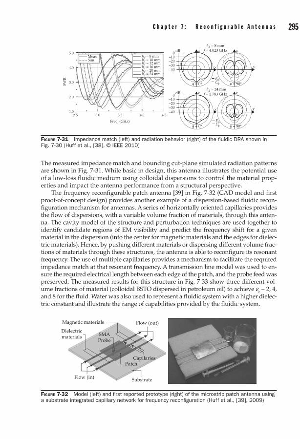
294 F r o n t i e r s i n a n t e n n a s : N e x t G e n e r a t i o n D e s i g n & e n g i n e e r i n g C h a p t e r 7 : r e c o n f i g u r a b l e a n t e n n a s 295
The measured impedance match and bounding cut-plane simulated radiation patterns are shown in Fig. 7-31. While basic in design, this antenna illustrates the potential use of a low-loss fluidic medium using colloidal dispersions to control the material prop-erties and impact the antenna performance from a structural perspective.
The frequency reconfigurable patch antenna [39] in Fig. 7-32 (CAD model and first proof-of-concept design) provides another example of a dispersion-based fluidic recon-figuration mechanism for antennas. A series of horizontally oriented capillaries provides the flow of dispersions, with a variable volume fraction of materials, through this anten-na. The cavity model of the structure and perturbation techniques are used together to identify candidate regions of EM visibility and predict the frequency shift for a given material in the dispersion (into the center for magnetic materials and the edges for dielec-tric materials). Hence, by pushing different materials or dispersing different volume frac-tions of materials through these structures, the antenna is able to reconfigure its resonant frequency. The use of multiple capillaries provides a mechanism to facilitate the required impedance match at that resonant frequency. A transmission line model was used to en-sure the required electrical length between each edge of the patch, and the probe feed was preserved. The measured results for this structure in Fig. 7-33 show three different vol-ume fractions of material (colloidal BSTO dispersed in petroleum oil) to achieve er ~ 2, 4, and 8 for the fluid. Water was also used to represent a fluidic system with a higher dielec-tric constant and illustrate the range of capabilities provided by the fluidic system.
Figure 7-31 Impedance match (left) and radiation behavior (right) of the fluidic DRA shown in Fig. 7-30 (Huff et al., [38], © IEEE 2010)
5.0
4.0
3.0
2.0
1.02.5 3.0 3.5 4.0 4.5
SWR
Freq. (GHz)
Meas.Sim
hd = 8 mm
hd = 8 mm
hd = 10 mmhd = 12 mmhd = 16 mmhd = 20 mmhd = 24 mm
dB0
–10–20–30–40
dB0
–10–20–30–40
z
z
x
EθEφ
EθEφ
x
y
y
z
z
f = 4.023 GHz
hd = 24 mmf = 2.783 GHz
φ = 0°
φ = 0°
φ = 90°
φ = 90°
Figure 7-32 Model (left) and first reported prototype (right) of the microstrip patch antenna using a substrate integrated capillary network for frequency reconfiguration (Huff et al., [39], 2009)
Magnetic materials
Dielectricmaterials
Substrate
PatchCapilaries
SMAProbe
Flow (out)
Flow (in)

296 F r o n t i e r s i n a n t e n n a s : N e x t G e n e r a t i o n D e s i g n & e n g i n e e r i n g C h a p t e r 7 : r e c o n f i g u r a b l e a n t e n n a s 297
7.3.5 Switching Speeds and Other ParametersThe speed or rate at which the reconfiguration mechanism can facilitate changes in the antenna is a very important design parameter. This requirement is typically imposed by the intended application and can ultimately determine the viability of a given design. In the broader and perhaps more general study of reconfigurable antenna technologies, speed may often be overlooked while attempting to understand a particular antenna topology or perhaps investigate a new design paradigm. However, the speed, as well as linearity, power handling capabilities, and other operational parameters of the recon-figuration mechanism will eventually manifest itself in the performance and ultimate utility of the reconfigurable antenna system.
Switches and other discrete mechanisms based on semiconductors such as PIN di-odes and FETs are commonly used in circuit and RF front ends. These control devices have very well characterized parameters. RF MEMS have also been investigated for some time to improve their reliability so their properties are becoming better understood. The values shown in Table 7-1 (adapted from [4]) provide a snapshot for comparison
Figure 7-33 Measured impedance match as a function of the colloidal dispersion properties in the capillaries (Huff et al., [39], 2009)
5.0
4.0
3.0
VSW
R
2.0
1.02.5 2.625 2.75 2.875 3 3.125 3.25
Freq. [GHz]
DI water
Petroleum distillate oil andcolloidal BaSr0.5Ti0.5O3
ϑ = 0 (εr = 2.1)ϑ = 0.25 (εr = 4.1)
ϑLimit ~ 0.925 (εr ~ 80)
ϑ = 0.5 (εr = 8.3)
Table 7-1 Switching Speeds of MEMS, Diodes, and FETs
Parameter RF MEMS PIN FET
Voltage [V] < 100 < 5 < 5
Switching time [s] 10−6 10−9 10−9
Isolation High Medium Low
Insertion Loss Low Medium Medium
Loss Low Medium High
Power Handling [W] > 1 > 10 > 10
Power Consumption Negligible Low Negligible
Linearity High Low Low
Adapted from Rebeiz, RF MEMS: Theory design and technology, John Wiley and Sons, 2003.

296 F r o n t i e r s i n a n t e n n a s : N e x t G e n e r a t i o n D e s i g n & e n g i n e e r i n g C h a p t e r 7 : r e c o n f i g u r a b l e a n t e n n a s 297
purposes of the trade-offs in performance metrics for PIN diodes, FETs, and RF MEMS. These values continue to change and improve from the antenna perspective by increasing speed, developing better linearity, and decreasing power consumption. However, this table still provides a glimpse into the trade-offs that must be made when choosing a given reconfiguration mechanism. This type of classification for enabling continuous tunability in antenna reconfiguration mechanisms is more challenging to define. The trends in MEMS, diodes, and FETs predominantly follow Table 7-1, but relaxation times in ferroic materials and fluidic displacement mechanisms are dependent on a number of parame-ters that are not reflected directly through the analysis on terminal devices. Of these two, ferroelectric devices hold a significant speed advantage. The more general question of speed is an ongoing field of investigation and discovery in the field of reconfigurable antennas.
7.4 Control, Automation, and ApplicationsThe properties of reconfigurable and multifunctional antennas and antenna systems are often derived from both expected theoretical outcomes and application-driven needs. The versatility of reconfiguration is highlighted in current and emerging application spaces that integrate the electromagnetic agility of reconfigurable antennas into the sys-tem performance to enhance functionality. Cognitive, smart, and adaptive systems, as well as communications and sensor networks, are broad areas that have channeled the development and implementation of these dynamic antenna systems and their sup-porting technologies [40]. This section examines the control and automation of the sys-tems as well as several recent examples of reconfigurable antenna applications.
The control and automation of reconfigurable antenna systems represents an equiva-lently important concern as their design and operation. Figure 7-34 illustrates a general-ized control scheme for reconfigurable antennas (adapted from [41]). This includes: the parasitic and driven elements of the antenna, the reconfiguration mechanisms from Fig. 7-1, the controller that collects feedback from the RF chain, any external sources, and the mechanism that delivers control signals and feedback to external sources. As the diagram suggests, the control signals delivered to reconfiguration mechanisms provide stimulus to initiate pattern or frequency reconfiguration. Feedback from sensor and other inputs along the RF chain are used with information from the transmit and receive module (T/R-module) and external sources to determine these control signals. This may be hardwired through logic devices and/or used in conjunction with an algorithm developed to opti-mize these capabilities in real-time or assist in intermediate frequency (IF) and post-pro-cessing operations.
Figure 7-34 Generalized control diagram for reconfigurable antennas (adapted from [41])
Transmit andreceive module
Phasecontrol
Powercontrol
Controller
Distributionmanifold
Reconfigurationmechanisms
Driven elementParasitic elementExternalfeedback
External input
Feedback Controlsignals

298 F r o n t i e r s i n a n t e n n a s : N e x t G e n e r a t i o n D e s i g n & e n g i n e e r i n g C h a p t e r 7 : r e c o n f i g u r a b l e a n t e n n a s 299
The self-optimizing real-time adaptive antenna system shown in Fig. 7-35 [42] pro-vides a very rudimentary but fundamental example of the automation and control of a reconfigurable antenna system. Three servomotors and evolutionary computation techniques are used in real time to find antenna positioning that optimizes the re-ceived signal strength. This system autonomously controls the position and rotation of the analog broadcast television V-dipole antenna commonly referred to as “bunny ears” (the V-dipole antenna has two elements that can rotate through two different axes on a rotating mount). The adaptability of this system is derived from a genetic algorithm (GA) [43] that has been modified to control the reconfigurable hardware in real time through a feedback circuit. The angular positions of the servo are encoded in this example as a chromosome in a GA population, and the signal strength is measured as a fitness to estimate the performance of each position. The resulting system pro-vided adaptation through reconfiguration by moving the elements to the best position as television channels were changed. The GA adjusted the V-dipole antenna position to find optimal reception. Albeit simplistic from an antenna design standpoint, the system in [42] blends very powerful real-time optimization techniques with reconfigu-rable antenna concepts to provide a functional system that demonstrates very powerful concepts.
Figure 7-35 Self-optimizing adaptive antenna system using real-time evolutionary computation techniques (genetic algorithm) to find antenna positioning that optimizes the received signal strength (images from [42])
Circuitry for signalmeasurement
Antenna positioningcircuitry

298 F r o n t i e r s i n a n t e n n a s : N e x t G e n e r a t i o n D e s i g n & e n g i n e e r i n g C h a p t e r 7 : r e c o n f i g u r a b l e a n t e n n a s 299
The ability to alter communication channel metrics (fading, correlation, etc.) and provide diversity gains in single and multiple antenna systems also creates many oppor-tunities for reconfigurable antenna systems [44]. A simple 2 × 2 multiple input multiple output (MIMO) system [45] illustrates the use of reconfigurable antennas in a multiple antenna system. Two frequency reconfigurable microstrip dipoles using PIN diode switches shown in Fig. 7-36 are used to control the interelement mutual coupling and far-field radiation patterns between antennas at both the receiver and transmitter. Numerical simulations in an urban environment were used to examine the performance of this an-tenna system. The link capacity in this situation is maximized by decreasing the spatial channel correlation through spatial multiplexing. As with the previous example, this type of reconfigurable antenna system is intended to sense the quality of transmission and to modify the antennas to maximize the rate at which information can be passed through the system. The example here shows a measurable gain in performance when compared to a fixed (non-reconfigurable) antenna system. This is illustrated in Fig. 7-37 by compar-ing the capacity of the fixed and reconfigurable antenna system at a location and by the percentage of improvement in capacity at the locations shown in Fig. 7-36.
Figure 7-36 Reconfigurable frequency microstrip dipoles using PIN diode switches (left) and ur-ban environment used to examine the performance of the 2 × 2 MIMO system (Piazza et al., [45], © IEEE 2008)
DC trace
PIN diode
Inductor
Resister
Capacitor
TX
RX
zy
x
Figure 7-37 Comparison of capacity between the fixed and reconfigurable antenna system (left) and percent improvement in capacity at the locations shown on the right side of Fig. 7-36 (Piazza et al., [45], © IEEE 2008)
Fixed antennaReconfig. antenna
1
0.9
0.8
0.7
0.6
0.5
0.4
0.3
0.2
0.1
0
Pr (c
apac
ity
< a
bsci
ssa)
8 9 10 11 12 13 14 15 16
Capacity (bps/Hz)
40
35
30
25
20
15
10
5
0
Perc
enta
ge C
apac
ity
Impr
ovem
ent
0 5 10 15 20 25 30
SNR [dB]
Location 1Location 2Location 3Location 4Location 5

300 F r o n t i e r s i n a n t e n n a s : N e x t G e n e r a t i o n D e s i g n & e n g i n e e r i n g C h a p t e r 7 : r e c o n f i g u r a b l e a n t e n n a s 301
The use of pattern reconfigurable antenna and direct modulation (DM) as per [46] provides a very different example of an emerging application of reconfigurable anten-nas. Figure 7-38 shows the simplified diagram of a traditional transmitter and DM con-figuration, which is implemented by the repeated switching of elements to synthesize digital symbols. This steers the information beam, or the beamwidth, over which decod-able information is sent, instead of steering the radiation pattern in a phased array con-figuration. This configuration is especially useful in secure communications since it can substantially disrupt the magnitude and phase information in the constellation for a given digital modulation technique. The use of reconfigurable antennas in this technique adds additional degrees of freedom into the use of DM since the pattern behavior can be used to enhance the distortion of signals in undesired locations. Two examples are shown in Fig. 7-39 using a quadrature phase-shift key (QPSK) modulation scheme and a four-element array of pattern reconfigurable antennas also shown in Fig. 7-39 [17]. The left and right sides of this figure show the resulting constellation of an eavesdropper in the direction of intended transmission and away from the direction of transmission. The DM and baseband modulation (shown as “traditional”) show little difference in the intended direction, but the constellation is severely degraded away from the direction of intended propagation. Power efficiency is not optimal in this example, but it represents a very novel use of reconfigurable antenna pattern diversity.
Figure 7-39 QPSK constellation diagrams comparing direct modulation (DM) with traditional (baseband) modulation in the direction of information beamforming (left) and away from the in-tended direction of information beamforming (right) (Daly et al., [46], © IEEE 2010)
DMTrad.
Q.
.I
DMTrad.
Q.
.I
Figure 7-38 Diagram of traditional baseband modulation (left) and direct modulation (dm) (right) (Daly et al., [46], © IEEE 2010)
Information
Beamsteeringcontrol
Basebandmodulation
fc
Traditional transmitter
Information Directionalmodulation
Directional modulation transmitter
fc

300 F r o n t i e r s i n a n t e n n a s : N e x t G e n e r a t i o n D e s i g n & e n g i n e e r i n g C h a p t e r 7 : r e c o n f i g u r a b l e a n t e n n a s 301
7.5 ReviewThe discussion on reconfigurable antenna technologies presented in this chapter covers many different areas. The basic properties of reconfigurable antennas were discussed first. This included the two defining characteristics—reconfigurable frequency and re-configurable radiation. These characteristics were assumed to be mutually exclusive from an operation standpoint, such that a radiation reconfigurable antenna would pro-vide this behavior over a common impedance bandwidth. Likewise, a frequency recon-figurable antenna would maintain a common pattern bandwidth throughout reconfig-uration. A brief discussion was also provided to illustrate the differences between direct reconfiguration and parasitic reconfiguration.
Next, numerous design examples were discussed to illustrate the emerging and burgeoning areas in reconfigurable antenna technologies. These were presented by way of the reconfiguration mechanism used to enable their operation. We began with elec-tromechanical mechanisms, which covered the use of RF MEMS, RF NEMS, electroac-tive polymers (EAPs), and piezoelectric materials. The use of semiconductor devices and materials were presented next, along with a brief discussion of photonic control. This was followed by ferroic materials. Fluidic reconfiguration provided the last mech-anism that was considered.
The control and automation of reconfigurable antenna systems was covered. This included a discussion of the closed-and-open loop systems as well as cognitive systems that can use the reconfigurable antenna properties as a means to adapt to changing environments. Applications of reconfigurable antenna systems followed this discussion and provided insight into a few of the emerging areas where the utilization of recon-figurable antennas has been shown to provide significant trade-offs in increased perfor-mance and complexity. The use of directional modulation techniques and multiple in-put multiple output (MIMO) illustrated two of these areas, but there are vastly more opportunities.
7.6 Final RemarksThe field of study that encompasses reconfigurable antennas provides numerous op-portunities for basic, applied, and advanced research. There is significant room for growth in this area, which is expanding as the capabilities of dynamic antennas are better understood and their ability to enhance system level performance becomes more widely recognized. In a broader context, the examples used throughout this chapter should illustrate that reconfigurable antennas also provide a very active test-bed for cross-disciplinary activities. This ranges from the development of tunable materials systems and composites, and micro- and nano-scale electromechanical sys-tems, all the way up to the synthesis of new radiating devices and use of existing structures as reconfigurable antennas themselves. At the system level this provides motivation for the development of algorithms that can maximize these reconfigu-rable capabilities. Given this broad scope of interest, the future of reconfigurable and multifunctional antennas or structures will continue to grow and enable new technologies.

302 F r o n t i e r s i n a n t e n n a s : N e x t G e n e r a t i o n D e s i g n & e n g i n e e r i n g C h a p t e r 7 : r e c o n f i g u r a b l e a n t e n n a s 303
ReferencesJ. T. Bernhard, “Reconfigurable antennas,” in [1] Synthesis Lectures on Antennas, vol. 4, C. A. Balanis, Ed., San Rafael, CA: Morgan & Claypool Publishers, 2007, pp. 1–66.G. H. Huff, and J. T. Bernhard, “Reconfigurable Antennas,” in [2] Modern antenna handbook, C. A. Balanis, Ed. Hoboken, NJ: John Wiley & Sons, Inc., 2007, pp. 369–398.Y. Imanaka, [3] Multilayered Low Temperature Cofired Ceramics (LTCC) Technology. New York, NY: Springer Publishing Company, 2005. I. D. Robertson, and S. Lucyszyn, [4] RFIC and MMIC Design and Technology. London, United Kingdom: The Institute of Electronics and Technology, 2001.G. M. Rebeiz, [5] RF MEMS: Theory, Design and Technology. Hoboken, NJ: John Wiley & Sons, Inc., 2003.R. S. Elliot, [6] Antenna Theory & Design. Hoboken, NJ: John Wiley & Sons, Inc., 2003.C. A. Balanis, [7] Antenna Theory: Analysis and Design. Hoboken, NJ: John Wiley & Sons, Inc., 2005.W. L. Stutzman, and G. A. Thiele, [8] Antenna Theory and Design. Hoboken, NJ: John Wiley & Sons, Inc., 1998.Y. T. Lo, and S. W. Lee, [9] Antenna Handbook. New Your, NY: Chapman and Hall, 1993.D. M. Pozar, and D. Schaubert, [10] Microstrip Antennas: The Analysis and Design of Microstrip Antennas and Arrays. Hoboken, NJ: John Wiley & Sons, Inc., 1995.R. F. Harrington, [11] Time Harmonic Electromagnetic Fields. Hoboken, NJ: John Wiley & Sons, Inc., 2001.J. A. Stratton, [12] Electromagnetic Theory. Hoboken, NJ: John Wiley & Sons, Inc., 2007.R. E. Collin, [13] Field Theory of Guided Waves. Hoboken, NJ: John Wiley & Sons, Inc., 1980.N. Marcuvitz, [14] Waveguide Handbook. Hoboken, NJ: John Wiley & Sons, Inc., 1951.R. Garg, [15] Analytical and Computational Methods in Electromagnetics. Norwood, MA: Artech House, Inc., 2008.W. Rotman and A. Maestri, “An electromechanically scannable trough waveguide array,” in proc. [16] IRE International Convention Record, Vol. 8, March 1960, pp. 67-83.G. H. Huff, and J. T. Bernhard, “Integration of packaged RF MEMS switches with radiation pattern [17] reconfigurable square spiral microstrip antennas,” IEEE Trans. Antennas Propag., vol. 54, part 1, pp. 464–469, Feb. 2006.Radant MEMS. SPST-RMSW100 RF-MEMS switch data sheet [Online]. Available: http://www [18] .radantmems.com/radantmems.data/Library/Radant-Datasheet100_1.7.pdf.H. Rajagopalan, Y. Rahmat-Samii, and W. A. Imbriale, “RF MEMS actuated reconfigurable reflectar-[19] ray patch-slot element,” IEEE Trans. Antennas Propag., vol. 56, pp. 3689–3699, 2008.B. A. Cetiner, G. R. Crusats, L. Jofre, and N. Biyikli, “RF MEMS integrated frequency reconfigurable [20] annular slot antenna,” IEEE Trans. Antennas Propag., vol. 58, pp. 626–632, 2009.N. Kingsley, D. E. Anagnostou, M. Tentzeris, and J. Papapolymerou, “RF MEMS sequentially recon-[21] figurable Sierpinski antenna on a flexible organic substrate with novel dc-biasing technique,” IEEE/ASME J. Microelectromech. Syst., vol. 16, pp. 1185–1192, 2007.J. Perruisseau-Carrier, and A. K. Skrivervik, “Monolithic MEMS-based reflectarray cell digitally recon-[22] figurable over a 360º phase range,” IEEE Antennas Wireless Propag. Lett., vol. 7, pp. 138–141, 2008.S. Penmetsa, Z. Tianhua, G. Zhongcheng, L. Tae-woo, and L. Que, “Design and modeling of a tunable [23] optical antenna enabled by a micromachined actuator,” in. 4th IEEE Int. Conf. Nano/Micro Eng. and Molecular Sys. (NEMS 2009), pp. 176–180, 2009.J.-C. Chiao, Y. Fu, I. Chio, M. DeLisio, and L.-Y. Lin, “MEMS reconfigurable Vee antenna,” [24] in IEEE MTT-S Int. Microwave Symp. Dig., Anaheim, CA, pp. 1515–1518, June 1999.A. Mahanfar, C. Menon, and R. G. Vaughan, “Smart antennas using electro-active polymers for [25] deformable parasitic elements,” Electron. Lett., vol. 44, pp. 1113–1114, 2008. S. H. Hsu, and C. Kai, “A novel reconfigurable microstrip antenna with switchable circular polariza-[26] tion,” IEEE Antennas Wireless Propag. Lett., vol. 6, pp. 160–162, 2007.F. Reggia, E. G. Spencer, R. D. Hatcher, and J. E. Tompkins, “Ferrod radiator system,” [27] Proc. IRE, vol. 45, pp. 344–352, 1957.V. K. Palukuru, M. Komulainen, T. Tick, J. Perantie, and H. Jantunen, “Low-sintering-temperature [28] ferroelectric-thick films: RF properties and an application in a frequency-tunable folded slot antenna,” IEEE Antennas Wireless Propag. Lett., vol. 7, pp. 461–464, 2008.K. C. Hwang, and J. E. Hyo, “Slot array antenna using a rectangular waveguide partially filled [29] with a ferrite slab,” in Proc. IEEE Int. Workshop Antenna Tech. Small Antennas Novel Metamaterials, pp. 412–415, 2006.M. L. VanBlaricum, “Photonic antenna reconfiguration: A status survey,” [30] Proc. SPIE Photonics Radio Freq. II, San Diego, CA, pp. 180–189, July 1998.

302 F r o n t i e r s i n a n t e n n a s : N e x t G e n e r a t i o n D e s i g n & e n g i n e e r i n g C h a p t e r 7 : r e c o n f i g u r a b l e a n t e n n a s 303
A. S. Nagra, O. Jerphagnon, P. Chavarkar, M. VanBlaricum, and R. A. York, “Indirect optical control [31] of microwave circuits using monolithic optically variable capacitors,” IEEE Trans. Microw. Theory Tech., vol. 47, pp. 1365–1372, July 1999.J. Sarrazin, Y. Mahe, S. Avrillon, and S. Toutain, “Pattern reconfigurable cubic antenna,” [32] IEEE Trans. Antennas Propag., vol. 57, pp. 310–317, Feb. 2009.G. H. Huff, T. L. Roach, and J. T. Bernhard, “Conformal integration of broadside to endfire radiation [33] reconfigurable antennas onto canonical structures,” Proc. IEEE/URSI Int. Symp. Antennas Propag., Monterey, CA, Vol. URSI, p. 138, June 2004.J. Perruisseau-Carrier, P. Pardo-Carrera, and P. Miskovsky, “Modeling, design and characterization [34] of a very wideband slot antenna with reconfigurable band rejection,” IEEE Trans. Antennas Propag., vol. 58, pp. 2218–2226.C. J. Panagamuwa, A. Chauraya, and J. C. Vardaxoglou, “Frequency and beam reconfigurable [35] antenna using photoconducting switches,” IEEE Trans. Antennas Propag., vol. 54, pp. 449–454, Feb., 2006. C. Chung-Hao, and D. Peroulis, “Liquid RF MEMS wideband reflective and absorptive switches,” [36] IEEE Trans. Microw. Theory Tech., vol. 55, pp. 2919–2929, Dec. 2007.A. Sihvola, [37] Electromagnetic Mixing Formulas and Applications. London, UK: Institute of Engineering and Technology, 1999.G. H. Huff, D. L. Rolando, P. Walters, and J. McDonald, “A Frequency reconfigurable dielec-[38] tric resonator antenna using colloidal dispersions,” IEEE Antennas Wireless Propag. Lett., vol. 9, pp. 288–290, 2010. G. H. Huff, S. Goldberger, and S. A. Long, “The RF cuttlefish: Overview of biologically inspired [39] concepts for reconfigurable antennas and smart skins,” Proc. Antenna Applicat. Symp., Monticello, IL, pp. 291–305, Sept. 2008.Y. Songnan, Z. Chunna, H. Pan, A. Fathy, and V. Nair, “Frequency-reconfigurable antennas for [40] multiradio wireless platforms,” IEEE Microwave, vol. 10, pp. 66–83, 2009.T. L. Larry, M. L. VanBlaricum, and A. S. Richen, US Patent Number 7 453 413, “Reconfigurable [41] parasitic control for antenna arrays and subarrays,” Nov 18, 2008.C. K. Oh, and B. K. Hanley, “Self-optimizing adaptive antenna,” U.S. Naval Research Lab, Washington, [42] DC, 2006. Available: http://www.nrl.navy.mil/content_images/06Information(Oh).pdfD. E. Goldberg, [43] Genetic Algorithms in Search, Optimization, and Machine Learning. Boston, MA: Kluwer Academic Publishers, 1989.R. Vaughan, and J. B. Andersen, [44] Channels, Propagation and Antennas for Mobile Communications, London, UK: Institute of Engineering and Technology, 2003. D. Piazza, N. J. Kirsch, A. Forenza, R. W. Heath, and K. R. Dandekar, “Design and evaluation [45] of a reconfigurable antenna array for MIMO systems,” IEEE Trans. Antennas Propag., vol. 56, pp. 869–881, 2008.M. P. Daly and J. T. Bernhard, “Beamsteering in pattern reconfigurable arrays using directional [46] modulation,” IEEE Trans. Antennas Propag., vol. 58, pp. 2259–2265.

This page intentionally left blank

CHAPTER 8Antennas in Medicine:
Ingestible Capsule Antennas
Harish Rajagopalan, Phillip M. Izdebski, and Yahya Rahmat-Samii
8.1 IntroductionThe use of electromagnetics in medicine has facilitated various medical treatments and diagnostic procedures [1]–[3]. Electromagnetic applications in biology and medicine can be broadly classified into two groups: (1) diagnostics—including magnetic reso-nance imaging (MRI) and tumor detection [4] and (2) therapeutics, which includes dia-thermy, hyperthermia for cancer therapy, and microwave angioplasty [5], [6]. Diseases of the gastrointestinal (GI) tract such as Crohn’s disease, ulcerative colitis, and intestinal bleeding are becoming common. The gastrointestinal (GI) tract is a 30-ft long structure that includes the esophagus, stomach, small intestines, colon, and rectum. Traditional endoscopy can only map the first 4 feet to the GI tract (gastroscope) and the last 6 feet of the tract (colonoscope) as shown in Fig. 8-la. The remaining 20 feet of the tract is un-reachable, preventing the early diagnosis of common diseases in the GI tract. Apart from this, these procedures create patient discomfort, often require anaesthesia, and impair patient mobility. As an alternative, a biomedical ingestible wireless capsule en-doscope has been developed [7]. The device was primarily developed to overcome the limitations of traditional endoscopy. The endoscope consists of a capsule the size of a vitamin pill containing a complementary metal oxide semiconductor (CMOS) camera imager, light-emitting diodes, a transmitter, batteries, an antenna, and sensors as shown in Fig. 8-lb [8], [9]. Once the capsule is swallowed, it travels through the GI tract passively and transmits video images out of the patient’s body through radiotelemetry.
Additionally, the capsule microsystems can be used as a sensor for monitoring the temperature and pressure of patients. The electronic digestible pill systems were first re-ported in 1950s [10] to measure temperature and later in the 1970s [11] for pH sensing. IDEAS and SmartPill are some of the multisensor microsystems that are utilized for sens-ing applications [12]. M2A capsule camera from Given Imaging and Norika capsule from Japan have been successfully used to retrieve video images of the GI tract [13], [14]. These capsule systems provide the exciting capability of transmitting biological statistics and vitals of patients and test subjects in real-time. They can also be employed in monitoring
305
306 F r o n t i e r s i n A n t e n n a s : N e x t G e n e r a t i o n D e s i g n & E n g i n e e r i n g C h a p t e r 8 : A n t e n n a s i n M e d i c i n e : I n g e s t i b l e C a p s u l e A n t e n n a s 307
the core temperature of athletes while transmitting up-to-date statistics to a receiver mon-itored by medical personnel to prevent heatstroke and other heat related injuries. These systems can also be used as actuators to provide drug delivery to patients. The Enterion capsule and ChipRx capsule are two examples of capsule that release drugs inside the GI tract [15]. Some of the limitations of these systems are restricted internal battery power supply, location estimation issues due to movement only by peristalsis, and a continuous communication link due to random orientation of the capsule [16], [17].
The development of a successful wireless link is an important requirement in making these smart pill systems efficient. Wireless technology is a key player in making this possible. In order to establish secure and stable communication links for these capsule devices, antennas that are placed inside and outside the human body need to be electro-magnetically characterized in detail [18], [19]. The challenge is to design a miniaturized antenna with effective performance to operate in the human body environment for these smart pill systems. This chapter discusses in detail the requirements to design a novel min-iaturized antenna for capsule systems which can be effectively integrated within the pill.
In the past, low-frequency coiled antennas have been used for biotelemetry in these capsules. But this inductive link is limited by slow data rates and a short range com-munication link between the medical device and the receiver. FCC has allocated new bands at higher frequencies to overcome some of these issues, which include 915 MHz industrial, scientific, and medical (ISM) bands and 1395–1400 MHz wireless medical
Figure 8-1 (a) Typical traditional endoscope used for mapping the first few feet of the GI tract. (b) The typical components found within capsule imaging system with overall dimensions 1.1 cm × 2.6 cm [8], [13].
1. Eyepiece2. Opening for wires and instruments3. Flexible shaft4. Flexible shaft transmitting air, water and light5. Flexible tip
(a)
1 23
4
5
Port forinstruments
Eyepiece
Esophagus
EndoscopeSteeringcontrol
Smallintestine
1 3
4
2
4
5 6 6 7 8
1. Optical dome2. Lens holder3. Short focal-length lens4. Light-emitting diodes5. CMOS imager6. Batteries7. Radio telemetry transmitter8. Antenna
(b)
UGI Tract
SmallIntestineColon
Esophagus
Stomach
Liver
Ascendingcolon
Illeum
Rectum Sigmoidcolon
Transversecolon
Smallintestine
Descendingcolon

306 F r o n t i e r s i n A n t e n n a s : N e x t G e n e r a t i o n D e s i g n & E n g i n e e r i n g C h a p t e r 8 : A n t e n n a s i n M e d i c i n e : I n g e s t i b l e C a p s u l e A n t e n n a s 307
telemetry services (WMTS) band. The advantages of the WMTS frequency band are that they provide the patients with greater mobility and increased comfort as there is no need to be connected to hospital equipment, and they also allow for the remote monitoring of several patients simultaneously.
The use of helical antennas has been proposed for these endoscopic devices [20]. These antennas are simple to design and operate in normal helix mode. However, due to the volumetric nature of the helix, a considerable amount of the capsule is oc-cupied by the antenna which may hinder possible capsule miniaturization. The most elegant antenna design solution for bio-capsule systems is to conform the antenna to the inside of the capsule shell [21]. This solution effectively utilizes the space within the cap-sule and also provides the possibility of integrating the antenna with the capsule pill. Many unique obstacles must be overcome to design a meaningful antenna for the cap-sule imaging system. Most critical are the physical size constraints limited by the dimen-sions of the capsule, approximately 1.1 cm × 2.6 cm, in conjunction with the necessary frequency band of 1395–1400 MHz allocated by the FCC for WMTS. Furthermore, the capsule contains many electrical components limiting the physical space within the cap-sule and causing possible coupling between the devices as shown in Fig. 8-1. Addition-ally, the location and orientation of the capsule vary with passage through the digestive track. Therefore, it is essential to have an omnidirectional radiation pattern with diverse polarization in order to ensure that a receiver will be able to receive the transmitted signal. Lastly, due to the electrical characteristics of the body, the design of the antenna must compensate for the differences between free space and the human body.
Figure 8-2 shows the detailed outline of the chapter and also shows the design methodology followed for successful capsule antenna design. Planar meandered dipoles
Figure 8-2 Schematic diagram showing the methodologies used for the design of ingestible capsule antennas for biotelemetry
Planar meanderedantennas
Ingestible antennas forcapsule bio-telemetry
Conformal antennain free space
Miniaturized antennainside human body
Link budget and SARBalanced planar meandered dipole
Offset planar meandered dipoleTheory and measurement
Space-filling naturePolarization senseRadiation Pattern
Miniaturized designRadiation pattern
Electrical components
SAR analysisLink estimation
Communication link comparisonSmall
intestineCapsuleantenna
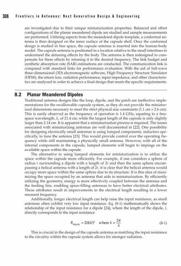
308 F r o n t i e r s i n A n t e n n a s : N e x t G e n e r a t i o n D e s i g n & E n g i n e e r i n g C h a p t e r 8 : A n t e n n a s i n M e d i c i n e : I n g e s t i b l e C a p s u l e A n t e n n a s 309
are investigated due to their unique miniaturization properties. Balanced and offset configurations of the planar meandered dipole are studied and sample measurements are performed. Utilizing aspects from the meandered dipole template, a conformal an-tenna is then designed on the inner surface of the capsule shell. Once the conformal design is studied in free space, the capsule antenna is inserted into the human-body model. The capsule antenna is positioned in a location relative to the small intestines to understand the detuning effects by the body. The antenna is then redesigned to com-pensate for these effects by retuning it to the desired frequency. The link budget and synthetic absorption rate (SAR) estimations are conducted. The communication link is compared with standard links for performance evaluation. With the aid of full-wave three-dimensional (3D) electromagnetic software, High Frequency Structure Simulator (HFSS), the return loss, radiation performance, input impedance, and other characteris-tics are analyzed in order to achieve a final design that meets the specific requirements.
8.2 Planar Meandered DipolesTraditional antenna designs like the loop, dipole, and the patch are ineffective imple-mentations for the swallowable capsule system, as they do not provide the miniatur-ized dimensions necessary to meet the strict physical size constraints (1.1 cm × 2.6 cm). This is easily observed as the frequency of operation is 1.4 GHz, equating to a free-space wavelength, l, of 21.4 cm, while the largest length of the capsule is only slightly larger than 2.14 cm. It is apparent that a miniaturization process is required. The issues associated with miniaturizing antennas are well documented in [22]. One possibility for designing electrically small antennas is using lumped components, inductors spe-cifically, to tune the antenna [23]. This would provide control over the operating fre-quency while still maintaining a physically small antenna. However, with all of the internal components in the capsule, lumped elements will begin to impinge on the available space within the capsule.
The alternative to using lumped elements for miniaturization is to utilize the space within the capsule more efficiently. For example, if one considers a sphere of radius r surrounding a dipole with a length of 2r and then the same sphere encom-passing a helical antenna with a length of 2r, it is clear that the helical antenna would occupy more space within the same sphere due to its structure. It is this idea of maxi-mizing the space occupied by an antenna that aids in miniaturization. By efficiently utilizing the geometry, energy is more effectively coupled between the antenna and the feeding line, enabling space-filling antennas to have better electrical attributes. These attributes result in improvements in the electrical length resulting in a lower resonant frequency.
Additionally, longer electrical length can help raise the input resistance, as small antennas often exhibit very low input resistance. Eq. (8-1) mathematically shows the relationship of the input resistance for a dipole [24], where the length of the dipole, l, directly corresponds to the input resistance
R kl kdipole = =2022( ) .whereπl (8-1)
This is crucial in the design of the capsule antenna as matching the input resistance to the circuitry within the capsule system allows for stronger radiation.

308 F r o n t i e r s i n A n t e n n a s : N e x t G e n e r a t i o n D e s i g n & E n g i n e e r i n g C h a p t e r 8 : A n t e n n a s i n M e d i c i n e : I n g e s t i b l e C a p s u l e A n t e n n a s 309
8.2.1 Balanced Planar Meandered Dipoles—TheoryThere are many options when considering space-filling antennas, such as the Hilbert curve fractal dipole, Minkowski fractal, Koch dipole, and many others [25]. However, the meandered dipole is preferred due to its vector current alignment, which aids in miniaturization [26]. This is visually shown in Fig. 8-3, where the currents in adjacent lines are always oriented in the same direction.
The necessity of the vector current alignment is based on increasing the self-inductance of the antenna. When the current vectors are in the same direction, the currents reinforce increasing the self-inductance and maximizing the decrease in resonant frequency for a given length. This is crucial for miniaturization, as the antenna’s small size makes it highly capacitive. A dipole, for instance, has the following reactance when it is much smaller than a half wavelength [24]:
X j klladipole = - -
-120 11( ) ln (8-2)
where a is the width of the dipole antenna. It is clearly seen that the dipole is capaci-tive, and it exhibits stronger capacitive characteristics when the length is miniaturized. To decrease the overall capacitance, the dipole must become more inductive, which can be accomplished by increasing the self-inductance between the lines in the meandered dipole. This increases the effective length of the antenna and in turn decreases the resonant frequency helping in overall miniaturization.
To explain the mutual inductance between the lines of the meandered dipole, an analysis on the adjacent parallel lines is conducted. Figure 8-4 shows a simplified mean-dered dipole with currents I1 and I2 and voltages V1 and V2.
The coupling between the lines is given by [27]
V L Lm1 0= +dIdt
dIdt
1 2 (8-3)
Figure 8-3 Meandered dipole structure showing current vector alignment for a center-fed meandered dipole
Figure 8-4 Explanation of currents, voltages, and inductances for the meandered dipole antenna
I2
I1
D
r+
r+
–
–
V1
V2

310 F r o n t i e r s i n A n t e n n a s : N e x t G e n e r a t i o n D e s i g n & E n g i n e e r i n g C h a p t e r 8 : A n t e n n a s i n M e d i c i n e : I n g e s t i b l e C a p s u l e A n t e n n a s 311
V L Lm2 0= +dIdt
dIdt
2 1 (8-4)
where Lm is the mutual inductance between the two lines and Lo is the self-inductance of each line independently. The following assumptions are made to simplify the analy-sis: (1) the self-inductances of both the lines are identical (similar dimensions), (2) the magnitude of the currents on the two lines is equal (minimal loss resistance), and (3) the phase of the currents is equal (the small dimensions of the line). This is easily ex-plained by understanding the phase of the current [28]:
phase frequencylength of antenna
speed= =w t∆ 2π . .
oof current on the conductor. (8-5)
Assuming a length of 40 mm for each arm and a conservative current speed of 90% the speed of light [29], the change in phase is approximately one degree. Using the approximations (I1 = I2 and V1 = V2) and simplifying (8-3) and (8-4), we get
V L L L Lm m1 01
01= + = +
dIdt
dIdt
dIdt
1 ( ) (8-6)
V L L L Lm m2 02
02= + = +
dIdt
dIdt
dIdt
2 ( ) (8-7)
As can be seen from (8-6) and (8-7), the inductance of each line is increased by Lm. However, in the extreme case where the currents are equal in magnitude but out of phase by 180°, I1 = -I2 and V1= -V2, the inductances of the lines will be reduced by the mutual inductance as given by
V L L L Lm m1 0 01= +
-= -
dIdt
d Idt
dIdt
1 1( )( ) (8-8)
V L L L Lm m2 0 02= +
-= -
dIdt
Idt
dIdt
2 2d( )( ) (8-9)
Now, with the understanding that the coupling between the lines helps in minia-turization, it is beneficial to see how the physical line geometry of the meandered dipole affects the mutual inductance. Mathematically, the relationship between parallel line geometry and the mutual inductance is given as [27]
Ll
D rm =-
-
µπ0
21In
2 (8-10)
where D is the distance between the adjacent lines, r is the radius of the lines, l is the length of the lines, and mo is the permeability of free space. By analyzing (8-10), the fol-lowing conclusions can be drawn between the geometry of the meandered dipole and mutual inductance:
• Thedistancebetweentheadjacentlinesisinverselyproportionaltothemutualinductance.
• Thelengthofthelinesisdirectlyproportionaltothemutualinductance.
• Theradiusofthelinesisinverselyproportionaltothemutualinductance.

310 F r o n t i e r s i n A n t e n n a s : N e x t G e n e r a t i o n D e s i g n & E n g i n e e r i n g C h a p t e r 8 : A n t e n n a s i n M e d i c i n e : I n g e s t i b l e C a p s u l e A n t e n n a s 311
Utilizing this analysis, a balanced meandered dipole was simulated in HFSS and later fabricated to validate the simulation results.
8.2.2 Balanced Planar Meandered Dipoles—Simulation and MeasurementFigure 8-5 shows the simulated design of the balanced meandered dipole at 1.4 GHz on a substrate with a dielectric constant of 2.2 and a thickness of 0.127 mm, a mi-crostrip line width of 0.3 mm, and 0.5 mm spacing amongst adjacent lines. Copper with a conductivity of 5.8 × 10⁷ S/m (copper) was used for the simulation purposes. The meandered dipole measures 29 mm × 5 mm, making it small enough to fit inside the capsule. To validate the simulation, the antenna was etched on RT/Duroid 5880 and fed by a quarter-wave balun. Due to a balanced structure, the impedance of the balanced meandered dipole antenna cannot be measured directly with a network ana-lyzer. This is because the feedpoints of the balanced antenna should be driven by equal and opposite currents, which is not true if the antenna is connected to an un-balanced coax port of the network analyzer. In order to measure the input impedance of this antenna, a quarter-wave balun was designed at the center frequency of 1.4 GHz. Figure 8-5c shows the prototype antenna and the balun used for impedance measure-ments. In order to make sure that the balun is carefully calibrated out of the measure-ment system the following procedure was conducted.
A cable, which was the exact same length of the balun, was used for calibration as seen in Fig. 8-5b. Once the short-open-load calibration was performed on the cable, the balun was connected to the network analyzer. The probe tips at the end of the balun were shorted together, and the electrical delay of the tips was adjusted accordingly
Figure 8-5 (a) Simulated balanced planar meandered antenna with overall dimensions of 2.9 cm × 0.5 cm. (b) Quarter-wave balun with probe tips and the same length cable for de-embedding the balun effect. (c) Balun connected to antenna feed location. (d) Simulated and measured return loss for the symmetric meandered dipole.
(a) (c)
SimMeas
0
–5
–10
–15
–201.2 1.3 1.4 1.5 1.6
Frequency (GHz)
S 11
(dB
)
(d)
5 mm
29.2 mm
(b)

312 F r o n t i e r s i n A n t e n n a s : N e x t G e n e r a t i o n D e s i g n & E n g i n e e r i n g C h a p t e r 8 : A n t e n n a s i n M e d i c i n e : I n g e s t i b l e C a p s u l e A n t e n n a s 313
on the network analyzer. This made sure that the calibration plane was at end points of the tips of the balun. The probe tips were then soldered to the antenna under test. It was confirmed that the balun was perpendicular to the antenna surface to minimize the coupling between the balun and the antenna. Using a network analyzer, the return loss was measured and compared to the HFSS results (Fig. 8-5d). The similarities be-tween the results verify the design; however, it also reveals that the matching of the meandered dipole to a 50 Ω line is not as desired (at least -10 dB) at resonance. This is attributed to the low radiation resistance of the antenna caused by miniaturization, as previously explained in (8-1). The intent of this measurement was to reveal the exis-tence of the resonance and understand the working of the balanced antenna. To rem-edy this, an offset meandered dipole was designed. Figure 8-6 shows the 3D radiation pattern of the resonant antenna, achieving its desired dipole-like behavior. The simu-lated total gain is given in dBi.
8.2.3 Offset Planar Meandered Dipoles—Simulation and MeasurementTo improve matching in the meandered dipole, the idea of an off-center feed is applied as illustrated in Fig. 8-7 [30]. This off-center feeding technique was once very popular
Figure 8-7 Meandered dipole structure showing current vector alignment for an offset fed meandered dipole
Figure 8-6 Simulated radiation pattern at 1.4 GHz for the meandered dipole located along the y-axis in the yz-plane. The longer dimensions of the dipole run parallel to the y-axis.
dB (gain total)–3.1159e–001–9.0244e–001–1.4933e+000–2.0841e+000–2.6750e+000–3.2658e+000–3.8567e+000–4.4475e+000–5.0384e+000–5.6292e+000–6.2201e+000–6.8109e+000–7.4018e+000–7.9926e+000–8.5835e+000–9.1743e+000–9.7652e+000
Theta
Z
Z
X
Y
Y
X Phi

312 F r o n t i e r s i n A n t e n n a s : N e x t G e n e r a t i o n D e s i g n & E n g i n e e r i n g C h a p t e r 8 : A n t e n n a s i n M e d i c i n e : I n g e s t i b l e C a p s u l e A n t e n n a s 313
with multiband antennas and is still often used in the HAM radio community [31]. The off-center fed antenna or Windom, named after its inventor Loren G. Windom, used a half-wavelength dipole with an offset feed to match the antenna to a single line con-ductor impedance of 600. By controlling this offset, he was able to achieve the desired impedance without the use of matching circuitry. In the same manner, the offset in the meandered dipole is applied to better match the antenna to a 50-Ω line. The current vectors are in the same direction, thus increasing the self-inductance and maximizing the decrease in resonant frequency for a given length as seen in Fig. 8-7.
To better appreciate this mechanism, a straight-wire dipole is simulated in HFSS. In Fig. 8-8b, the return loss of a straight-wire center-fed dipole is plotted. The resonance is observed at 700 MHz, which corresponds to the frequency at which the dipole is a half-wavelength (first resonance). However, by offsetting the feed by l /4 from the center [29], [30], a second resonance now occurs at 1.4 GHz in addition to the first reso-nance as seen in Fig. 8-8b. This is a result of the sinusoidal current distribution on the dipole, shown in Fig. 8-8a, where at 1.4 GHz the dipole electrical length is a full wave-length, resulting in a current that is minimal at the center of the dipole (a resistance corresponding to infinite resistance). Thus, by positioning the feed away from the center by l /4, the feed is closer to maximum current and therefore results in a smaller feed-point resistance that is significantly better matched to the 50-Ω. feed. This same con-cept is applied to the meandered dipole, where creating an offset between the two arms of the dipole results in an off-center feed that can be tuned to create better matching.
From Fig. 8-9b, it is observed that the offset meandered dipole creates two reso-nances and the second resonance is tuned to 1.4 GHz. Figure 8-9c shows the balun connected to the fabricated antenna for measurement. Figure 8-9d shows good agree-ment between the measurement and simulation for the frequency of interest. Figure 8-10 illustrates the dipole-like radiation pattern of the meandered dipole at the series resonance, which is omnidirectional in the xz-plane, complying with the design goals of the capsule antenna.
Figure 8-8 (a) Current distribution for a straight-wire dipole in free space in both center (solid) and offset (dashed) fed configurations. (b) Simulated resonance behavior of a straight-wire dipole fed at the center and offset by l /4.
Center-fedOffset-fed
Dipole
λ/2 center-fed
λ/4 offset-fed
0
–5
–10
–15
–200.6 0.8 1
Frequency (GHz)
S 11
(dB
)
1.2 1.4 1.6
(a) (b)
Second resonance
First resonance

314 F r o n t i e r s i n A n t e n n a s : N e x t G e n e r a t i o n D e s i g n & E n g i n e e r i n g C h a p t e r 8 : A n t e n n a s i n M e d i c i n e : I n g e s t i b l e C a p s u l e A n t e n n a s 315
Figure 8-9 (a) Simulated offset planar meandered antenna with overall dimensions of 2.9 cm × 0.5 cm. (b) Simulated S
11 for an offset fed meandered dipole at 1.4 GHz. (c) Balun connected to
antenna feed location. (d) Simulated and measured return loss for the asymmetric meandered dipole.
29.2 mm
(a) (c)
5 mm
S 11
(dB
)
SimMeas
0
–5
–10
–15
–201.2 1.3 1.4 1.5 1.6
Frequency (GHz)
S 11
(dB
)
(d)
1.21.11 1.3 1.4 1.5 1.6Frequency (GHz)
(b)
0
–5
–10
–15
–20
First resonance
Second resonance
Figure 8-10 Simulated radiation pattern at 1.4 GHz for the offset meandered dipole located along the y-axis in the yz-plane. The longer dimensions of the dipole run parallel to the y-axis.
dB (gain total)–3.1159e–001–9.0244e–001–1.4933e+000–2.0841e+000–2.6750e+000–3.2658e+000–3.8567e+000–4.4475e+000–5.0384e+000–5.6292e+000–6.2201e+000–6.8109e+000–7.4018e+000–7.9926e+000–8.5835e+000–9.1743e+000–9.7652e+000
Theta
Z
Z
X
YX
Y
Phi
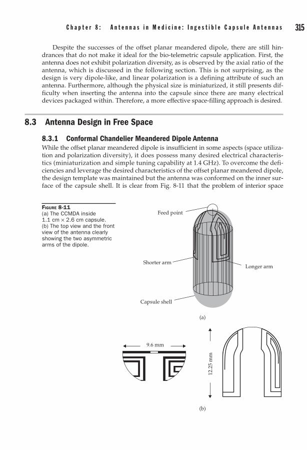
314 F r o n t i e r s i n A n t e n n a s : N e x t G e n e r a t i o n D e s i g n & E n g i n e e r i n g C h a p t e r 8 : A n t e n n a s i n M e d i c i n e : I n g e s t i b l e C a p s u l e A n t e n n a s 315
Despite the successes of the offset planar meandered dipole, there are still hin-drances that do not make it ideal for the bio-telemetric capsule application. First, the antenna does not exhibit polarization diversity, as is observed by the axial ratio of the antenna, which is discussed in the following section. This is not surprising, as the design is very dipole-like, and linear polarization is a defining attribute of such an antenna. Furthermore, although the physical size is miniaturized, it still presents dif-ficulty when inserting the antenna into the capsule since there are many electrical devices packaged within. Therefore, a more effective space-filling approach is desired.
8.3 Antenna Design in Free Space
8.3.1 Conformal Chandelier Meandered Dipole AntennaWhile the offset planar meandered dipole is insufficient in some aspects (space utiliza-tion and polarization diversity), it does possess many desired electrical characteris-tics (miniaturization and simple tuning capability at 1.4 GHz). To overcome the defi-ciencies and leverage the desired characteristics of the offset planar meandered dipole, the design template was maintained but the antenna was conformed on the inner sur-face of the capsule shell. It is clear from Fig. 8-11 that the problem of interior space
Figure 8-11 (a) The CCMDA inside 1.1 cm × 2.6 cm capsule. (b) The top view and the front view of the antenna clearly showing the two asymmetric arms of the dipole.
Feed point
Shorter armLonger arm
Capsule shell
(a)
(b)
9.6 mm
12.2
5 m
m

316 F r o n t i e r s i n A n t e n n a s : N e x t G e n e r a t i o n D e s i g n & E n g i n e e r i n g C h a p t e r 8 : A n t e n n a s i n M e d i c i n e : I n g e s t i b l e C a p s u l e A n t e n n a s 317
consumption is now alleviated. The conformal “chandelier” meandered dipole antenna (CCMDA) accomplishes this by making use of the natural geometry of the capsule, enabling the interior of the capsule to be empty. Nevertheless, the conformal geometry was still limited as it was important not to obstructing the optical dome of the lens system depicted in Fig. 8-11b. To avoid this problem, the chandelier design was intentionally built on only half of the pill, utilizing half of the cylinder and one of the spherical dome ends, Fig. 8-11a. The feed point, offset configuration, and capsule shell can be clearly seen in Fig. 8-11a. This design was simulated on the inner surface of the capsule shell so that that the copper conductor is insulated from direct contact with human tissues. The actual capsule for this application is generally made of a very thin (0.1 mm) polyethylene/gelatin shell and coated with a bio-compatible layer that is resistant to stomach acids [13]. For simplicity, the dielectric constant of the capsule shell is assumed to be 2.2 (polyethyl-ene). It should be noted that the antenna parameters can be tuned accordingly depending on the contents (dielectric constant) of the capsule shell. The elegance of this design is that it does not use any space inside the capsule volumetrically, thus making miniaturization of the whole system possible. Also, these antennas can be potentially etched/printed on the inner surface of the capsule shell as part of capsule development. Another advantage of this design is that it can be tuned to any impedance (currently 50 Ω) for other potential applications like radio frequency identification (RFID) pills within the human body [33].
It is important to verify that the electrical characteristics of the offset planar mean-dered dipole did not severely alter with the conformal bending. This is not expected, as bends to an antenna do not vary the current excitation of the antenna [34]. To verify this, HFSS simulations of the CCMDA were performed to analyze the electrical characteristics in comparison with the planar meandered dipole. Figure 8-12a clearly shows that the return loss for the offset planar meandered dipole and conformal chandelier design is very similar. This is expected, as the chandelier design was built with identical total wire length, spacing, line thickness, and offset between the two arms. Additionally, the capsule was assumed to be a simple plastic with a permittivity of 2.2 and a thickness of 100 microns, almost equal to that of the substrate used in the offset planar meandered scenario. Figure 8-12b shows the real and imaginary part of the input impedance for the CCMDA. It can be clearly seen that the real part of input impedance has a good match to 50 Ω at the second resonance. Figure 8-13 shows the radiation pattern for the conformal design;
Figure 8-12 (a) Simulated return loss comparisons between planar offset meandered antenna and the chandelier antenna. (b) Input impedance of the chandelier antenna in free space.
S 11
(dB
)
1.21.11 1.3 1.4 1.5 1.6Frequency (GHz)
(a)
0
–5
–10
–15
–20
Offset planar meanderConformal chandelier In
put i
mpe
dan
ce (O
hms)
1.21.11 1.3 1.4 1.5 1.6Frequency (GHz)
(b)
400300
200
100
0–100
–200–300
–400
ReactanceResistance
Second resonanceFirst resonance
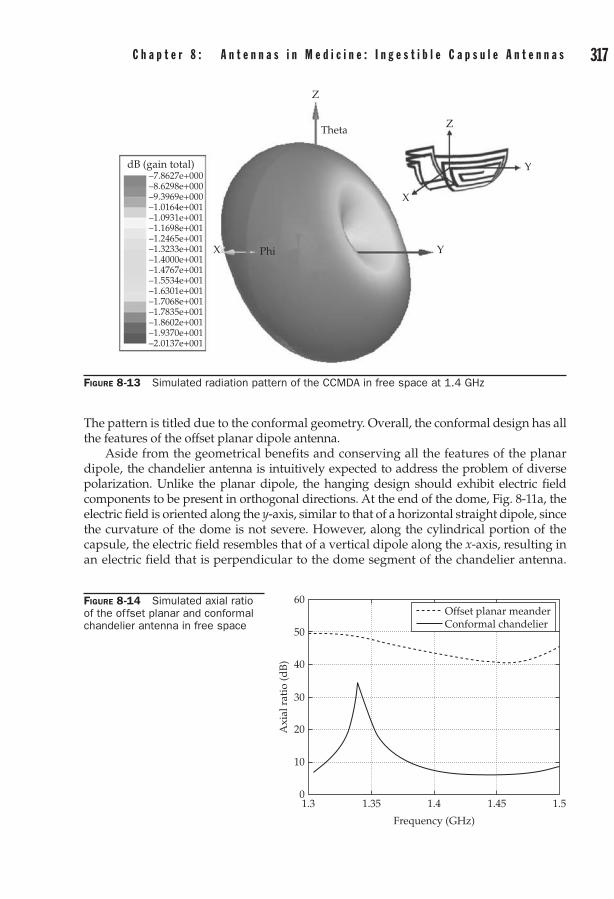
316 F r o n t i e r s i n A n t e n n a s : N e x t G e n e r a t i o n D e s i g n & E n g i n e e r i n g C h a p t e r 8 : A n t e n n a s i n M e d i c i n e : I n g e s t i b l e C a p s u l e A n t e n n a s 317
The pattern is titled due to the conformal geometry. Overall, the conformal design has all the features of the offset planar dipole antenna.
Aside from the geometrical benefits and conserving all the features of the planar dipole, the chandelier antenna is intuitively expected to address the problem of diverse polarization. Unlike the planar dipole, the hanging design should exhibit electric field components to be present in orthogonal directions. At the end of the dome, Fig. 8-11a, the electric field is oriented along the y-axis, similar to that of a horizontal straight dipole, since the curvature of the dome is not severe. However, along the cylindrical portion of the capsule, the electric field resembles that of a vertical dipole along the x-axis, resulting in an electric field that is perpendicular to the dome segment of the chandelier antenna.
Figure 8-14 Simulated axial ratio of the offset planar and conformal chandelier antenna in free space
60Offset planar meanderConformal chandelier
50
40
30
20
10
01.3 1.35 1.4 1.45 1.5
Axi
al r
atio
(dB
)
Frequency (GHz)
Figure 8-13 Simulated radiation pattern of the CCMDA in free space at 1.4 GHz
dB (gain total)–7.8627e+000–8.6298e+000–9.3969e+000–1.0164e+001–1.0931e+001–1.1698e+001–1.2465e+001–1.3233e+001–1.4000e+001–1.4767e+001–1.5534e+001–1.6301e+001–1.7068e+001–1.7835e+001–1.8602e+001–1.9370e+001–2.0137e+001
Theta
Z
Z
X
YX
Y
Phi
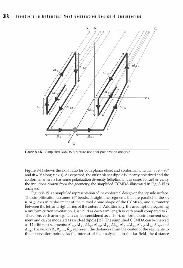
318 F r o n t i e r s i n A n t e n n a s : N e x t G e n e r a t i o n D e s i g n & E n g i n e e r i n g C h a p t e r 8 : A n t e n n a s i n M e d i c i n e : I n g e s t i b l e C a p s u l e A n t e n n a s 319
Figure 8-14 shows the axial ratio for both planar offset and conformal antenna (at q = 90° and Φ = 0° along x-axis). As expected, the offset planar dipole is linearly polarized and the conformal antenna has some polarization diversity (elliptical in this case). To further verify the intuitions drawn from the geometry, the simplified CCMDA illustrated in Fig. 8-15 is analyzed.
Figure 8-15 is a simplified representation of the conformal design on the capsule surface. The simplification assumes 90° bends, straight line segments that are parallel to the x-, y, or z- axis in replacement of the curved dome shape of the CCMDA, and symmetry between the left and right arms of the antenna. Additionally, the assumption regarding a uniform current excitation, I, is valid as each arm length is very small compared to l. Therefore, each arm segment can be considered as a short, uniform electric current seg-ment and can be modeled as an ideal dipole [35]. The simplified CCMDA can be viewed as 12 different segments: ∆LR1, ∆LR2, ∆LR3, ∆LR4, ∆LR5, ∆LR6, ∆LL1, ∆LL2, ∆LL3, ∆LL4, ∆LR5, and ∆LR6. The vectors
rR 1,
rR 2, ...,
rRn, represent the distances from the center of the segments to
the observation points. As the interest of the analysis is in the far-field, the distance
Figure 8-15 Simplified CCMDA structure used for polarization analysis
R1 R2
Y
Z
Rn
∆LR3
∆LR4
∆LR6
∆LR2∆LR5
∆LR1
∆LL2
∆LL6
∆LL5
∆LL1
X
∆LL3∆LL4
...........
318 F r o n t i e r s i n A n t e n n a s : N e x t G e n e r a t i o n D e s i g n & E n g i n e e r i n g C h a p t e r 8 : A n t e n n a s i n M e d i c i n e : I n g e s t i b l e C a p s u l e A n t e n n a s 319
vectors become essentially parallel [32] and equal in magnitude, r. However, the phase of the distance vectors has the general form of
R r r r≅ - ′r . ˆ (8-11)
where ′rr is the vector from the coordinate origin to the center of each segment and r is the
unit vector from the origin to the observation point. The phases of the distance vectors are:
RR1
= r - g1
RL1
= r + g1
RR2
= r - g2
RL2
= r + g2
RR3
= r - g3
RL3
= r + g3
RR4
= r - g4
RL4
= r + g4
RR5
= r - g5
RL5
= r + g5
RR6
= r - g6
RL6
= r + g6
The gamma terms are used to represent the general expression, rr´⋅ r, for each
segment. As the structure has left and right arms that are equivalent, the gamma terms for equivalent right and left arms are the same but of opposite polarity.
Since each segment is represented by a z-directed infinitesimal dipole centered at the origin, the magnetic vector potential is given by [35]
rA
I Lr
e zjkr≈ -µπ∆
4ˆ. (8-12)
The individual far-field magnetic vector potential contributions due to the 12 segments are therefore given by
r rA
I Lr
e y AI L
reR
jk rL
j1
11
1
4 41≈ ≈- - -µ
πµπ
g∆ ∆( )( ˆ ) kk r r
Rjk r
L
y
AI L
re x A
( )
( )
( ˆ )
( ˆ)
+
- -≈ -
1
22
2
4
r rµπ
g∆22
2
33
4
4
2≈
≈
- +
-
µπ
µπ
gI Lr
e x
AI L
re
jk r
Rjk
∆
∆
( )
(
( ˆ)
rrr
Ljk r
R
z AI L
re z
A
- - +≈ -
≈
g gµπ
3 33
3
4
4) ( )( ˆ) ( ˆ)
r
r
∆
µµπ
µπ
gI Lr
e x AI L
rejk r
Ljk r∆ ∆4
44
4 44- - - +≈( ) (( ˆ)
rgg
gµπ
µ
4
55
554
)
( )
( ˆ)
( ˆ)
-
≈ - ≈- -
x
AI L
re z AR
jk rL
r r∆ II Lr
e z
AI L
re
jk r
Rjk r
∆
∆
5
66
4
4
5
π
µπ
g
g
- +
- -≈
( )
(
( ˆ)
r66 6
66
4) ( )( ˆ) ( ˆ)- ≈ - +x A
I Lr
e xLjk r
r µπ
g∆

320 F r o n t i e r s i n A n t e n n a s : N e x t G e n e r a t i o n D e s i g n & E n g i n e e r i n g C h a p t e r 8 : A n t e n n a s i n M e d i c i n e : I n g e s t i b l e C a p s u l e A n t e n n a s 321
Combining the x-, y-, and z-directed terms yields
rA
I Lr
e eI L
xjk r jk r= - +- + - -µ
πµπ
g g∆ ∆2 4
4 42 2( )( ) ( )
rre e
I Lr
e
jk r jk r
jk r
( )
(
( ) ( )
(
- - - +
- +
-
+
g g
gµπ
4 4
6
4∆
66 6) ( ) )- - -e jk r g
(8-13)
rA
I Lr
e eyjk r jk r= +- - - +µ
πg g∆ 1
41 1( )( ) ( ) (8-14)
rA
I Lr
e eI L
zjk r jk r= - +- - - +µ
πµπ
g g∆ ∆3 5
4 43 3( )( ) ( )
rre ejk r jk r( ).( ) ( )- + - --g g5 5 (8-15)
Using Euler’s formula, the vector potentials are simplified to be
rA j
Ier
L L Lx
jkr
= + --
24 2 2 4 4 6
µπ
g g[ sin( ) sin( ) s∆ ∆ ∆ iin( )]g 6 (8-16)
rA
I L ery
jkr
=-
24
11
µπ
g∆
cos( ) (8-17)
rA j
Ier
L Lz
jkr
= --
24 3 3 5 5
µπ
g g[ sin( ) sin( )].∆ ∆ (8-18)
The electric far-fields can be computed simply by the relationship between the electric field and the magnetic vector potential using e jwt time, convention [35]
r rE j A= - ω . (8-19)
As evident by the analysis, there will be electric field components in the x-, y-, and z-directions, unlike that of the planar conformal dipole, which contains fields in only the x- and y-directions. For both the CCMDA and the planar meandered dipole, this provides one of the conditions for circular polarization: there are at least two orthogo-nal linear components in the electric field. More importantly however, the vector poten-tials for the CCMDA reveal that
rAy is 90° out of phase with
rAx and
rAz potentials.
This provides the second necessary condition for circular polarization: at least two elec-tric field components have a time-phase difference of odd multiples of 90°. The planar meandered dipole does not exhibit this behavior, which is expected as it resembles that of a simple dipole, which is well known to be linearly polarized. The third condition for circular polarization is that the orthogonal components have equal magnitude. Since this is not the case as evident by the arm lengths, elliptical polarization is ex-pected as a result. Although this is not the ideal polarization, it does provide a vast improvement over the planar meandered dipole. To confirm this analysis, HFSS sim-ulations for the CCMDA and planar meandered dipole were conducted. Figure 8-16 and Fig. 8-17 show the electric far-field components for planar dipole antenna and the conformal dipole antenna. As expected, the CCMDA contains electric fields in all three directions, while the planar meandered dipole exhibits an electric field in only the y-direction.
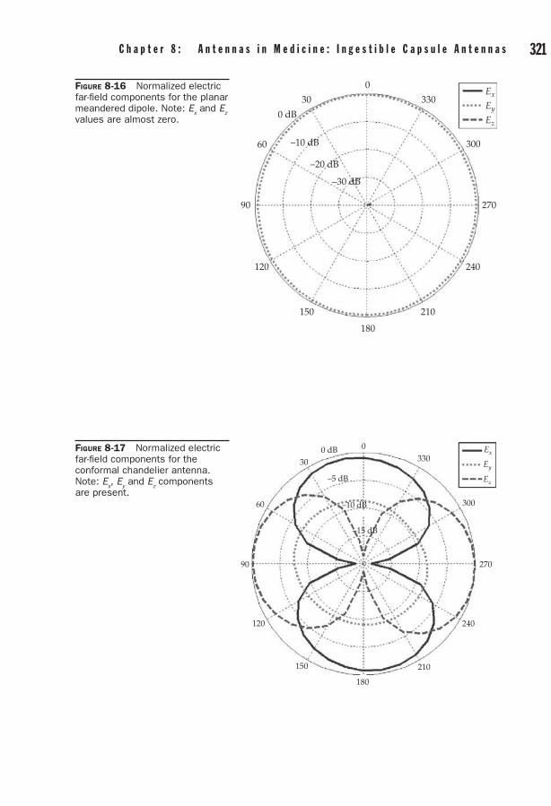
320 F r o n t i e r s i n A n t e n n a s : N e x t G e n e r a t i o n D e s i g n & E n g i n e e r i n g C h a p t e r 8 : A n t e n n a s i n M e d i c i n e : I n g e s t i b l e C a p s u l e A n t e n n a s 321
Figure 8-16 Normalized electric far-field components for the planar meandered dipole. Note: E
x and E
z
values are almost zero.
330Ex
Ey
Ez
300
270
240
210
180
150
120
90
60
30
0 dB
–10 dB
–20 dB
–30 dB
0
Figure 8-17 Normalized electric far-field components for the conformal chandelier antenna. Note: E
x, E
y and E
z components
are present.
Ex330
Ey
Ez
300
270
240
210
180
150
120
90
60
300 dB
–10 dB
–5 dB
–15 dB
0
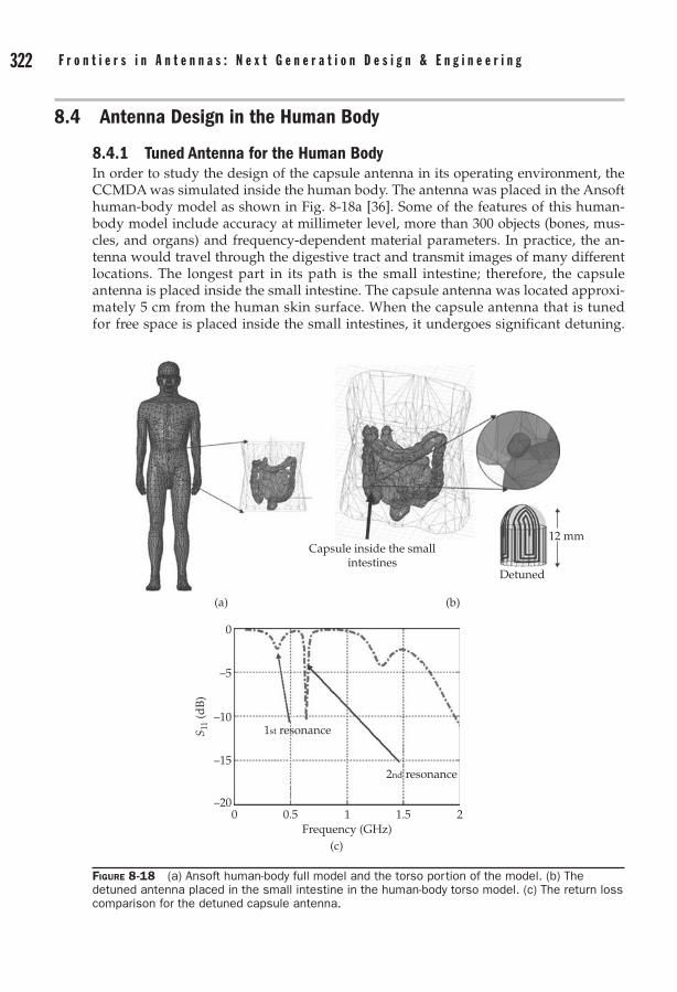
322 F r o n t i e r s i n A n t e n n a s : N e x t G e n e r a t i o n D e s i g n & E n g i n e e r i n g C h a p t e r 8 : A n t e n n a s i n M e d i c i n e : I n g e s t i b l e C a p s u l e A n t e n n a s 323
8.4 Antenna Design in the Human Body
8.4.1 Tuned Antenna for the Human BodyIn order to study the design of the capsule antenna in its operating environment, the CCMDA was simulated inside the human body. The antenna was placed in the Ansoft human-body model as shown in Fig. 8-18a [36]. Some of the features of this human-body model include accuracy at millimeter level, more than 300 objects (bones, mus-cles, and organs) and frequency-dependent material parameters. In practice, the an-tenna would travel through the digestive tract and transmit images of many different locations. The longest part in its path is the small intestine; therefore, the capsule antenna is placed inside the small intestine. The capsule antenna was located approxi-mately 5 cm from the human skin surface. When the capsule antenna that is tuned for free space is placed inside the small intestines, it undergoes significant detuning.
Figure 8-18 (a) Ansoft human-body full model and the torso portion of the model. (b) The detuned antenna placed in the small intestine in the human-body torso model. (c) The return loss comparison for the detuned capsule antenna.
Capsule inside the smallintestines
Detuned
12 mm
0
–5
–10
–15
–200 0.5 1
Frequency (GHz)21.5
S 11
(dB
)
1st resonance
2nd resonance
(a) (b)
(c)

322 F r o n t i e r s i n A n t e n n a s : N e x t G e n e r a t i o n D e s i g n & E n g i n e e r i n g C h a p t e r 8 : A n t e n n a s i n M e d i c i n e : I n g e s t i b l e C a p s u l e A n t e n n a s 323
The variation of dielectric constant and conductivity with frequency was incorporated into the human-body model. The dielectric constant varied from 58.9 to 55.9 and the conductivity varied from 2.2 S/m to 2.7 S/m for frequency range from 1 GHz to 1.8 GHz. The first resonance is now shifted close to 350 MHz while the second resonance is present at 600 MHz as shown in Fig. 8-18c. Although the capsule shell isolates the antenna from the human tissues, the wideband behavior can be attributed to the con-ductivity of the human body, and the large detuning is attributed to the drastic change of permittivity between free space and the human body. Because of this change in per-mittivity, the electrical length of the antenna is essentially elongated, and consequently, the CCMDA must be tuned to operate at the desired frequency.
The advantage of using this conformal meandered antenna is that the effect of detuning can be compensated by simply changing the length of the dipole arms. The antenna was tuned by shortening the length of the arms until the desired frequency was achieved. Figure 8-19a shows the miniaturized tuned antenna design with all the param-eters labeled. Figures 8-19b and 8-19c show the input impedance and return loss performance of the antenna inside the human-body model, respectively. It can be seen that when the length parameter is changed from 1.6 mm to 2.4 mm, there is very good matching at the frequency of interest (1.4 GHz) as shown in Fig. 8-19c. The conductivity of the human body helps in broadening the bandwidth of the antenna. Thus, it is observed that by simply altering the length if the two dipole arms, the antenna can be matched to any part of the human body. The final dimensions of the tuned CCMDA are 25.2 mm for the shorter offset arm and 42 mm for the longer arm of the antenna. The first resonance for the tuned antenna was close to 600 MHz and the second resonance (frequency of interest) was at 1.4 GHz as shown in Fig. 8-19d.
Figure 8-20a shows the electric field distribution at the surface of the human-body model. The antenna is placed close to 5 cm from the surface of the model roughly in the location of the small intestine. The location of the antenna can be easily identified from the hot spot at the surface. Figure 8-20b shows the radiation pattern cuts in the xz- and yz-planes. The peak gain at 1.4 GHz is about -28.4 dBi. The average gain value in the yz-plane (from 0° to 180°) was computed to be approximately -33.5 dBi (1W in-put power) and used for link budget calculations.
The capsule antenna along with the human body acts as a radiator. The radiation ef-ficiency of the whole system (antenna-human) is about 0.05%. Figure 8-20c shows the 3D radiation properties of the antenna within the human-body model. Due to the body conductivity, the losses in the antenna are high. The antenna along with the body acts as a transmitter causing significant attenuation of the radiated pattern. Maximum radiation is directed outward from the body toward free space. There is significantly less radiation in the backside of the body due to the orientation of the antenna. This behavior is expected and corresponds to results that were obtained for a different antenna configuration placed within the human head in [18].
8.4.2 Effect of Electrical Components on the Antenna PerformanceFrom the design of the capsule system, it is clear that the capsule has many electrical components packaged inside. It is important to study how these components affect the conformal antenna performance within the human body. The tuned chandelier design was intentionally built on only half of the pill, utilizing one of the spherical dome ends (to avoid camera obstruction). Due to this implementation, it is apparent that the batteries are the most significant electrical components to consider due to their size
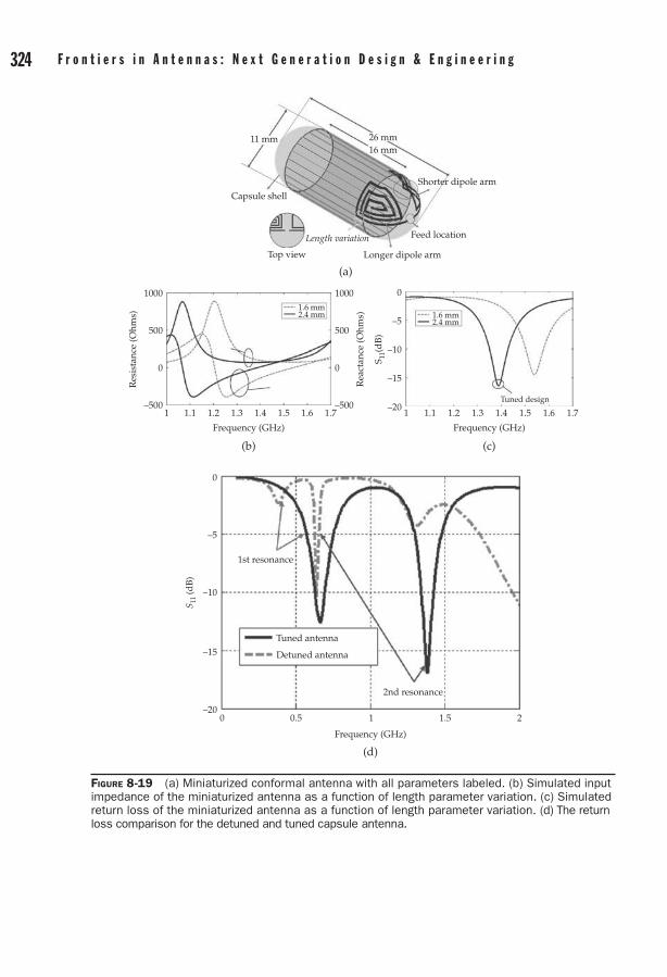
324 F r o n t i e r s i n A n t e n n a s : N e x t G e n e r a t i o n D e s i g n & E n g i n e e r i n g C h a p t e r 8 : A n t e n n a s i n M e d i c i n e : I n g e s t i b l e C a p s u l e A n t e n n a s 325
Figure 8-19 (a) Miniaturized conformal antenna with all parameters labeled. (b) Simulated input impedance of the miniaturized antenna as a function of length parameter variation. (c) Simulated return loss of the miniaturized antenna as a function of length parameter variation. (d) The return loss comparison for the detuned and tuned capsule antenna.
11 mm 26 mm16 mm
Shorter dipole arm
Feed location
Longer dipole arm
Length variation
Top view
Capsule shell
1000 0
–5
–10
–15
–20
500
0
–500
1000
500
0
–500
Res
ista
nce
(Ohm
s)
Rea
ctan
ce (O
hms)
S 11(d
B)
1 1.1 1.2 1.3
Frequency (GHz)
(b)
(a)
(c)
1.4 1.5 1.6 1.7 1 1.1 1.2 1.3
Frequency (GHz)
1.4 1.5 1.6 1.7
1.6 mm2.4 mm 1.6 mm
2.4 mm
Tuned design
0
–5
–10
–15
–20
S 11 (d
B)
Frequency (GHz)
(d)
1.5 210.50
Tuned antenna
Detuned antenna
2nd resonance
1st resonance
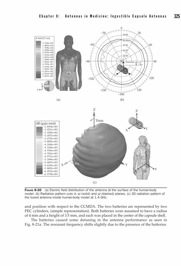
324 F r o n t i e r s i n A n t e n n a s : N e x t G e n e r a t i o n D e s i g n & E n g i n e e r i n g C h a p t e r 8 : A n t e n n a s i n M e d i c i n e : I n g e s t i b l e C a p s u l e A n t e n n a s 325
and position with respect to the CCMDA. The two batteries are represented by two PEC cylinders, (simple representation). Both batteries were assumed to have a radius of 4 mm and a height of 3.5 mm, and each was placed in the center of the capsule shell.
The batteries caused some detuning in the antenna performance as seen in Fig. 8-21a. The resonant frequency shifts slightly due to the presence of the batteries.
Figure 8-20 (a) Electric field distribution of the antenna at the surface of the human-body model. (b) Radiation pattern cuts in xz (solid) and yz (dashed) planes. (c) 3D radiation pattern of the tuned antenna inside human-body model at 1.4 GHz.
dB (gain total)–2. 8054e+001–3. 0221e+001–3. 2389e+001–3. 4557e+001–3. 6725e+001–3. 8892e+001–4. 1060e+001–4. 3228e+001–4. 5396e+001–4. 7563e+001–4. 9731e+001–5. 1899e+001–5. 4067e+001–5. 6235e+001–5. 8402e+001–6. 0570e+001–6. 2738e+001
Z
Theta
Z
Z
Y
Y
X
X
YPhiX
E field [Y/m]
5. 1000e+0012. 9882e+0011. 7508e+0011. 0258e+0016. 0104e+0003. 5216e+0002. 0633e+0001. 2089e+0007. 0833e–0014. 1502e–0012. 4316e–0011. 4247e–0018. 3477e–0024. 8910e–0022. 8657e–002
Z
X
0
30
60
90
120
150–180
–150
–120
–90
–60
–30
–40.00
–50.00
–60.00
–70.00
Y
–30.00
X
ZΦ = 0°Φ = 90°
(a) (b)
(c)

326 F r o n t i e r s i n A n t e n n a s : N e x t G e n e r a t i o n D e s i g n & E n g i n e e r i n g C h a p t e r 8 : A n t e n n a s i n M e d i c i n e : I n g e s t i b l e C a p s u l e A n t e n n a s 327
It can be clearly seen that the antenna has maintained its nearly circular polarization characteristics and the batteries do not affect the polarization performance significantly as seen in Fig. 8-21b. The radiation patterns were also computed at the respective reso-nant frequencies for the no-battery and battery case, respectively. There was a slight change in the radiation pattern due to the presence of batteries. This minor detuning in the presence of the batteries can be simply compensated by altering the antenna dimensions as discussed earlier (increasing the length of the arms).
8.5 SAR Analysis and Link Budget Analysis
8.5.1 Simple Human-Body ModelTo understand the performance of the antenna in a bio-telemetric system, Specific Ab-sorption Rate (SAR) study and link budget analysis were conducted in HFSS. The tuned miniaturized capsule antenna was once again placed inside the small intestine of the Ansoft human-body model as shown in Fig. 8-22a. Due to the detailed meshing and the elaborate model, computation time was large for the analysis of the antenna inside the human-body model. Therefore, a simplified human torso box model (measuring 30 cm × 60 cm × 40 cm) was developed as shown in Fig. 8-22b. A permittivity of 54.12
Figure 8-21 The effect of batteries on the antenna performance. (a) Return loss, (b) Axial ratio, (c) Radiation pattern. Note: All the results compare empty-capsule and capsule-with-batteries.
Antenna without batteriesAntenna with batteries
Antenna without batteriesAntenna with batteries
0
–5
–10
–20
–15S 11
(dB
)
–250.6 1 1.4
Frequency (GHz)
(a) (b)
(c)
1.8
20
15
10
5
0
Axi
al r
atio
(dB
)
1.2 1.3 1.4 1.5Frequency (GHz)
1.6
Almost CP
XX
XX
Z Z
ZZ
Y YYY
PhiPhi
Theta Theta
PECcylinders
dB (gain total)
–2. 8054e+001–3. 0531e+001–3. 3009e+001–3. 5486e+001–3. 7964e+001–4. 0441e+001–4. 2919e+001–4. 5396e+001–4. 7873e+001–5. 0351e+001–5. 2828e+001–5. 5306e+001–5. 7783e+001–6. 0261e+001–6. 2738e+001

326 F r o n t i e r s i n A n t e n n a s : N e x t G e n e r a t i o n D e s i g n & E n g i n e e r i n g C h a p t e r 8 : A n t e n n a s i n M e d i c i n e : I n g e s t i b l e C a p s u l e A n t e n n a s 327
and a conductivity of 1.14 S/m were applied to the box model, resembling that of a human muscle at 1.4 GHz [18]. The capsule antenna was placed 5 cm from the surface of the box model (approximately in the center of the small intestine). Figure 8-22 shows that the simple box model is a good approximation for the Ansoft human-body mod-el, especially for the frequency of interest (1.4 GHz). The simple box model produces similar results to human-body model; it saves computation time, and therefore, it is used for SAR and link budget analysis.
8.5.2 Specific Absorption Rate AnalysisSpecific Absorption Rate (SAR) is an important parameter in the design of antennas for biomedical systems as it determines the rate at which energy is absorbed by the human body when exposed to an electromagnetic field.
SAR (W/kg) is calculated from the electric field and is given by the following equa-tion
SAR (W / kg) =
12σρ
| |E 2
where s is the electrical conductivity of the tissue, E is the peak electric field and r is the density of the tissue. The SAR value depends on the location of the source and also
Figure 8-22 (a) HFSS human-body model (b) Simple homogeneous human-body model (c) Return loss comparison between HFSS and simple human-body model
Human modelBox model
0
–5
–15
–10
S 11
(dB
)
–200 0.5 1
Frequency (GHz)(c)
(a) (b)
1.5 2
Region of interest
Z
Y
X30 cm
40 cm
60 cm
2.6 cm
Capsule shell εr = 2.2
1.1 cm
Muscle compositionf = 1.4 GHzεr = 54.12σ = 1.14 S/m

328 F r o n t i e r s i n A n t e n n a s : N e x t G e n e r a t i o n D e s i g n & E n g i n e e r i n g C h a p t e r 8 : A n t e n n a s i n M e d i c i n e : I n g e s t i b l e C a p s u l e A n t e n n a s 329
on the geometry of the body. To calculate the possible maximum acceptable power delivered by the designed ingestible antenna in the simple body model, the peak 1-g SAR limitation (1.6 mW/g =1.6 W/kg) of ANSI is applied. Figure 8-23 shows the maxi-mum SAR values computed as a function of distance from the tip of the capsule an-tenna for normalized input power of 1W. A maximum SAR of 330 W/Kg (immediately outside the capsule shell) is computed. Away from the antenna, the SAR decreases rapidly (from 330 W/kg to 100 W/kg for a distance of 1 cm). In order to satisfy the peak 1-g SAR limitation (1.6 W/kg) of ANSI, the antenna can deliver a maximum power of 4.8 mW. With radiation efficiency of approximately 0.1%, the maximum possible radi-ated power will be about 4.8 µW (< 25 µW ERC limit). 1W power is used for normaliza-tion; in reality the power delivered to the antenna will be lower than 1W and typically in the range of 100µW.
8.5.3 Link Budget CharacterizationFor a reliable wireless link in the capsule endoscope system, there must be a robust con-nection between the transmitter and the receiver at all times especially when the an-tenna is residing in the small intestine. This will ensure real-time mapping of the small intestine and help in detection of bleeding or inflammation of the small intestine. Generally, the frame (image) size is 256 × 256 pixels and the data is transmitted at 2 frames per sec. A data rate of at least 1 Mbps (256 × 256 × 8 × 2) is required for successful real-time wireless communication. The capsule antenna system is typically
Figure 8-23 (a) Max SAR computed as a function of distance from the tip of the capsule antenna for normalized input power of 1W. (b) 1-g SAR distribution (0 dB = 10 × log (1 mW/g)) for 1W input power at three different locations from the tip of the capsule.
400
300
100
200
Max
SA
R (W
/K
g)
010 2
Distance from the capsule (cm)
(a)
(b)
3 4 5
2
1
3
Human body
1.1 cmDistance
2.6 cmCapsule shell εr = 2.2
30
10
–10
–3052.5 0 0 2.5
5–2.5 –2.5–5 –5
SAR
(dB
)
z (cm) x (cm)
20
10
0
–10
–20
SAR max = 25.1 dB
130
10
–10
–3052.5 0 0 2.5
5–2.5 –2.5–5 –5
SAR
(dB
)
z (cm) x (cm)
20
10
0
–10
–20
SAR max = 20.7 dB
230
10
–10
–3052.5 0 0 2.55
–2.5 –2.5–5 –5
SAR
(dB
)
z (cm) x (cm)
20
10
0
–10
–20
SAR max = 4.2 dB
3
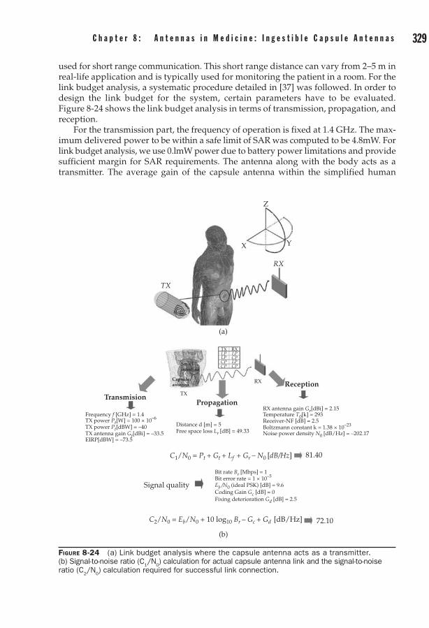
328 F r o n t i e r s i n A n t e n n a s : N e x t G e n e r a t i o n D e s i g n & E n g i n e e r i n g C h a p t e r 8 : A n t e n n a s i n M e d i c i n e : I n g e s t i b l e C a p s u l e A n t e n n a s 329
used for short range communication. This short range distance can vary from 2–5 m in real-life application and is typically used for monitoring the patient in a room. For the link budget analysis, a systematic procedure detailed in [37] was followed. In order to design the link budget for the system, certain parameters have to be evaluated. Figure 8-24 shows the link budget analysis in terms of transmission, propagation, and reception.
For the transmission part, the frequency of operation is fixed at 1.4 GHz. The max-imum delivered power to be within a safe limit of SAR was computed to be 4.8mW. For link budget analysis, we use 0.lmW power due to battery power limitations and provide sufficient margin for SAR requirements. The antenna along with the body acts as a transmitter. The average gain of the capsule antenna within the simplified human
Figure 8-24 (a) Link budget analysis where the capsule antenna acts as a transmitter. (b) Signal-to-noise ratio (C
1/N
0) calculation for actual capsule antenna link and the signal-to-noise
ratio (C2/N
0) calculation required for successful link connection.
Z
Y
RX
TX
TX
RX
(a)
(b)
X
Reception
Transmision
Signal quality
C1/N0 = Pt + Gt + Lf + Gr – N0 [dB/Hz]
C2/N0 = Eb/N0 + 10 log10 Br – Gc + Gd [dB/Hz]
PropagationRX antenna gain Gr[dBi] = 2.15
Free space loss Lr [dB] = 49.33Distance d [m] = 5
Temperature T0[k] = 293Frequency f [GHz] = 1.4TX power Pt[W] = 100 × 10–6
TX power Pt[dBW] = –40TX antenna gain Gt[dBi] = –33.5EIRP[dBW] = –73.5
Receiver-NF [dB] = 2.5
Bit rate Br [Mbps] = 1
Fixing deterioration Gd [dB] = 2.5
Bit error rate = 1 × 10⁻⁵
Coding Gain Gc [dB] = 0Eb /N0 (ideal PSK) [dB] = 9.6
Boltzmann constant k = 1.38 × 10⁻²³
Noise power density N0 [dB/Hz] = –202.17
TX RXLP LP
LPCP
CP
LPCPCP
81.40
72.10
Smallintestine
Capsuleantenna

330 F r o n t i e r s i n A n t e n n a s : N e x t G e n e r a t i o n D e s i g n & E n g i n e e r i n g C h a p t e r 8 : A n t e n n a s i n M e d i c i n e : I n g e s t i b l e C a p s u l e A n t e n n a s 331
model is about -33.5 dBi. The average gain is valid in the region, 0° < Φ <180° and 0°< q < 180° is shown in Fig. 8-24a. The total EIRP is less than the 25µW (-46 dBW) set by the European Research Council limitation. For the propagation part, the indoor communication distance is fixed at 5m. The free space loss for the 5m distance was 49.33 dB. For the receiver part, a linearly polarized antenna with a typical gain of 2.15 dBi (monopole) is assumed to be at the receiver. The noise power density was set at -202.17 dB/Hz for the ambient temperature of 293K (for noise power calculations refer [37]). The actual link has a signal to noise ratio (C1/N0) of 81.40 dB/Hz (computed using simple Friis formula).
Using communication theory, an estimate for the required link is developed. The bit rate and bit error rate are fixed at 1 Mbps ad 1 × 10 -5, respectively. Eb/N0 is defined as the ratio of Energy per Bit (Eb) to the Spectral Noise Density (N0) and is known as the signal-to-noise ratio for a digital communication system. Different modulation schemes have different Eb/N0 values depending on the bit error rate values. For PSK, for the above mentioned bit error rate, Eb/N0 is 9.6 dB. The required link, C2/N0, developed is 72.10 dB/Hz. Therefore, C1/N0 > C2/N0 (with a margin of about 10 dB), so successful wireless communication can be achieved. It can be noticed that in order to increase the range of transmission and the bit rate, the power transmitted can be increased (within safe SAR limit).
8.5.4 Link Budget for Free Space—Friis vs. HFSSA free-space link is developed at 1.4 GHz between two l0/2 (free-space wavelength) di-poles in order to get a better understanding of actual link and estimation of path loss calculation. The in-body capsule link will be compared to the free-space link in the next section. The transmitting antenna is delivered 1W of power (power of 1W is used for normalization purposes; in reality the power delivered to the antenna will be lower than 1W and typically in the range of l00µW). The dipoles are 9.6 cm in length. The distance between the transmitting and receiving antennas is varied from 20 cm to 30 cm (these distances are dictated by the computational domain). The far-field distance for the transmit antenna is about 9 cm (2D2/l). Figure 8-25a shows the Friis transmission for-mula for line-of-sight operation in free space at 1.4 GHz. For the transmission part, the transmit power is fixed at 1W and the transmit antenna gain is 2.15 dBi. For the propa-gation part, the free-space loss is 21.4 dB for 20 cm distance between the transmitting and receiving dipole. Figures 8-25b and 8-25c show the S11(dB) and S22(dB) for the trans-mitting and receiving dipoles, respectively. Figure 8-25d shows the S21(dB) between the two antennas. It can be clearly seen that when the distance between the antennas increases, the coupling reduces. Figure 8-25e shows the power received (dBm) at the receiver for various distances at 1.4 GHz. The HFSS computation and Friis formula show excellent matching. By developing a good understanding of the free-space link, the in-body links can be studied in detail.
8.5.5 Comparison Between Three Wireless Communication Links
8.5.5.1 Line-of-Sight OperationAs shown in Fig. 8-26a, three communication links were established: an ingestible capsule communication link, a free-space link, and an ingestible dipole link. The free-space link is between two l0/2 (free-space wavelength) dipoles. The in-body dipole link is between an ingestible dipole antenna (in a cylindrical insulator) in the human

330 F r o n t i e r s i n A n t e n n a s : N e x t G e n e r a t i o n D e s i g n & E n g i n e e r i n g C h a p t e r 8 : A n t e n n a s i n M e d i c i n e : I n g e s t i b l e C a p s u l e A n t e n n a s 331
Figure 8-25 (a) Friis transmission formula for line-of-sight operation in free space. (b) S11
(dB) for different distances between TX and RX. (c) S
22(dB) for different distances between TX and RX.
(d) S21
(dB) for different distances between TX and RX. (e) Power received at the receiver for different distances for line-of-sight operation. Note: A delivered power of 1W is used for normalization purposes.
0
–2
–4
–6
–8
–10S 11
(dB
)
–16
–12
–14
1 1.1 1.2 1.3 1.4
Frequency (GHz)(b) (c)
1.5 1.6 1.7 1.8
20 cm25 cm30 cm
–15
–20
–25
–30
S 21
(dB
)
–45
–35
–40
1 1.1 1.2 1.3 1.4
Frequency (GHz)
(d) (e)
1.5 1.6 1.7 1.8
20 cm25 cm30 cm
30
20
10
–10
0
Pow
er r
ecei
ved
(dB
m)
–20
–3020 21 22 23 24 25
Distance (cm)
26 27 28 29 30
0
–2
–4
–6
–8
–10S 22
(dB
)
–16
–12
–14
1 1.1 1.2 1.3 1.4
Frequency (GHz)
1.5 1.6 1.7 1.8
20 cm25 cm30 cm
Friis formulaHFSS
ReceptionTransmission
Propagation
R = 20 – 30 cm
Free space loss Lr [dB] = –21.4Distance d [m] = 0.2
Frequency f [GHz] = 1.4Frequency f [GHz] = 1.4
TX power Pt [W] = 1TX power Pt [dBW] = 0TX antenna gain Gt [dBi] = 2.15
RX antenna gain Gt [dBi] = 2.15
Frisstransmissionformula
(a)
Pr = Pt + Gt + Lf + Gr
λ0/2 λ0/2
body and a l0/2 dipole in free-space. The in-body capsule link is between an in-gestible capsule antenna (on the interior of the capsule shell) in the human body and a l0/2 dipole in free space. The antennas inside the human body are tuned to reso-nate at 1.4 GHz. The performances of all the three communication links are estimated

332 F r o n t i e r s i n A n t e n n a s : N e x t G e n e r a t i o n D e s i g n & E n g i n e e r i n g C h a p t e r 8 : A n t e n n a s i n M e d i c i n e : I n g e s t i b l e C a p s u l e A n t e n n a s 333
when the transmitting antennas are delivered 1W of power (power of 1W is used for normalization purposes).
Figure 8-26b shows the dimensions of all the antennas used. The dipoles for the free-space link are 9.6 cm in length. The in-body dipole length is 4 cm and the insulating cylinder, which prevents direct contact between the transmitting dipole and human body, has a radius of 0.08 cm and length of 4.4 cm. The conformal capsule antenna has a total length of approximately 7 cm and is conformed on a capsule shell with dielectric constant 2.2 and dimensions 2.6 cm × 1.1 cm. The capsule shell thickness is approximately 0.02 cm. The exterior receiving dipole is 9.6 cm in length. The distance between the transmitting and receiving antennas is varied from 20 cm to 30 cm (these distances are dictated by the computational domain). Both the antennas inside the hu-man body are located 5 cm from the surface of the skin (box model), roughly in the position of the small intestine.
Figure 8-27 shows the radiation patterns of the transmitting antennas for the three communications links at 1.4 GHz. The gain of the free-space TX antenna is 2.15 dBi
Figure 8-26 (a) Free-space link, in-body dipole link, and in-body capsule antenna. (b) Dimensions of the antennas: free-space antenna, in-body dipole, and in-body capsule. (c) The location of the TX and RX antennas in the link model.
TX
λ0/2 λ0/2 λ0/2 λ0/2
Dipole9.6 cm
Dipole4 cm
Insulatingcylinder(εr = 3, 4.4 cm)
Capsule shell(εr = 2.2, 0.02 cm)
0.16 cm
2.6 cm
1.1 cm
40 cm
30 cm
RXTX
X Y
Z
R2
R1
RX TX(a)
(b)
(c)
TXRX RX

332 F r o n t i e r s i n A n t e n n a s : N e x t G e n e r a t i o n D e s i g n & E n g i n e e r i n g C h a p t e r 8 : A n t e n n a s i n M e d i c i n e : I n g e s t i b l e C a p s u l e A n t e n n a s 333
(typical dipole). When the dipole is placed inside human body, the gain of the total transmitting system (dipole + human body) is approximately -29 dBi along the y-di-rection. When the capsule antenna is placed inside human body, the gain of the total transmitting system (capsule antenna + human body) is approximately -34 dBi along the y-direction. Figure 8-28 shows the maximum available power (dBm) at the re-ceiver dipole from the dipole in free space, the dipole inside box model, and the
Figure 8-27 (a) The radiation pattern of TX antenna for free-space link. (b) The radiation pattern of TX antenna for in-body dipole link. (c) The radiation pattern of TX antenna for in-body capsule antenna link (frequency = 1.4 GHz). Note: The radiation pattern and the gain values for the in-body dipole and in-body capsule antenna include both the antenna and human body.
dB (gain total)2.2870e+000
–1.0665e+000–4.4201e+000–7.7736e+000–1.1127e+001–1.4481e+001–1.7834e+001–2.1188e+001–2.4541e+001–2.7895e+001–3.1248e+001–3.4602e+001–3.7956e+001–4.1309e+001–4.4663e+001–4.8016e+001–5.1370e+001
dB (gain total)
dB (gain total)
–2.8118e+001–3.0489e+001
–3.2575e+001–3.4913e+001–3.7252e+001–3.9590e+001–4.1929e+001–4.4267e+001–4.6606e+001–4.8944e+001–5.1283e+001–5.3622e+001–5.5960e+001–5.8299e+001–6.0637e+001–6.2976e+001–6.5314e+001–6.7653e+001–6.9992e+001
–3.2859e+001–3.5229e+001–3.7599e+001–3.9969e+001–4.2339e+001–4.4710e+001–4.7080e+001–4.9450e+001–5.1820e+001–5.4190e+001–5.6560e+001–5.8931e+001–6.1301e+001–6.3671e+001–6.6041e+001
Phi
Phi
Phi
X
X
X
Y
Y
Y
Z
Z
Z
Theta
Theta
Theta
–120
–150
–180150
120
90
60
30
0
–30.00
–40.00
–50.00
–60.00
Φ = 0°Φ = 90°
–30
–60
–90
(a)
(c)
(b)
–120
–150–180
150
120
90
60
300
–30.00
–40.00
–50.00
–60.00
Φ = 0°Φ = 90°
–30
–60
–90
–120
–150–180
150
120
90
60
300
0.00–10.00–20.00–30.00–40.00–50.00
Φ = 0°Φ = 90°
–30
–60
–90

334 F r o n t i e r s i n A n t e n n a s : N e x t G e n e r a t i o n D e s i g n & E n g i n e e r i n g C h a p t e r 8 : A n t e n n a s i n M e d i c i n e : I n g e s t i b l e C a p s u l e A n t e n n a s 335
Figure 8-28 (a) Orientation of the TX and RX antennas for all three links. (b) Comparison of the maximum available power at the receiver from the three links. The operation is line-of-sight. Note: A delivered power of 1W is used for normalization purposes.
TX RX
Link 1
Link 2
Link 3
Z
Y
X
30
20
10
0
–10
–302220
(a)(b)
24
Distance (cm)
26 28 30
–20
Pow
er r
ecei
ved
(dB
m)
–40 dBm
–30 dBm
Free-spaceIn-body dipoleIn-body capsule
capsule antenna inside box model. The maximum available power (dBm) for the free-space link can also be calculated using simple Friis formula [35]. The maximum avail-able power difference between the free-space link and the in-body dipole link is about 30 dBm, which can be explained by the gain difference in the two links. Thus, the dif-ference between free-space and ingestible links can be explained from the radiation efficiencies of the TX antennas. The receiver must have sensitivity better than -30 dBm in order to pick up signal from capsule antenna for this short range (20–30 cm). The actual input power depends on peak SAR limitation and other constraints (bat-tery life) for ingestible devices.
8.5.5.2 Angle Dependence of the LinkWhen one has a linearly polarized receiver system, maintaining a reliable wireless com-munication link is a challenging task. Therefore, polarization diversity is an attractive attribute to have for the transmitting antenna. This diversity will help establish a link even if the TX and RX antennas are orthogonal to each other. Therein lies the inherent advantage of having the conformal antenna in the capsule instead of a loop or a straight dipole. The transmitting antennas for all the three links are rotated in the yz-plane as can be seen in Fig. 8-29a. It can be seen that when the transmitting dipole is orthogonal to receiving dipole for free-space link, no power is received. For the dipole in-body link, the received power consistently drops as the angle of rotation increases. But, for the in-body capsule link, the power received is almost constant regardless of the angle of rotation due to the capsule antenna’s polarization diversity (almost CP) as seen in Fig. 8-29a. In order to test the robustness of the in-body capsule link, the distance between the capsule antenna and the receiver was fixed at 20 cm and the in-body capsule antenna was rotated in three different planes. The capsule antenna was rotated from 0° to 90° in the yz-, xy-, and xz-planes, respectively, as shown in Fig. 8-29b. The received power showed a maximum variation of less than 5 dB for the different rotations.

334 F r o n t i e r s i n A n t e n n a s : N e x t G e n e r a t i o n D e s i g n & E n g i n e e r i n g C h a p t e r 8 : A n t e n n a s i n M e d i c i n e : I n g e s t i b l e C a p s u l e A n t e n n a s 335
On the other hand, the link budget developed earlier had a 10 dB difference between the required link and the actual link. This clearly validates that the conformal antenna has polarization diversity, and it makes the link more robust with respect to the capsule orientation.
In order to test the worst case scenario, the in-body capsule antenna is placed along -y-direction. Figure 8-30 shows the electric field distribution on the front and back faces of the simplified human model when the antenna is along in +y and -y-direction. It can clearly seen that when the antenna is facing in the +y-direction, the E field distribution on the front surface is greater than when it is placed along -y. The average gain in the region, 0° < Φ < 180° and 0°< q < 180°, decreases from -33.5 dBi to -45 dBi when the antenna orientation is changed from +y-axis to -y-axis. The communication link reduces to approximately 1.25 m in order to maintain the same 10-dB margin be-tween actual link (C1/N0) and required link (C2/N0).
Figure 8-29 (a) Comparison of the maximum available power at the receiver from the three links when the transmitting antennas rotate in the yz-plane, (b) Comparison of the maximum available power at the receiver from the in-body capsule link when the capsule is rotated in three different planes (yz, xy, and xz). Note: A delivered power of 1W is used for normalization purposes.
302010
0–10–20–30–40
Pow
er r
ecei
ved
(dB
m)
–50–60–70–80
10 20 30 40Angle-YZ plane (°)
50 60 70 80 900
302010
0–10–20–30–40
Pow
er r
ecei
ved
(dB
m)
–50–60
–70–80
10 20 30 40Angle (°)
50 60 70 80 900
Free-spaceIn-body dipoleIn-body capsule
XY-planeYZ-planeXZ-plane
Approximately 5 dB variation
No received power
TX
Z
Z
Z
X
X
X
Y
Y
Y
Z
X
Y
RX
Link 1
Link 2
Link 3
YZ plane
XZ plane
XY plane
(b)
(a)

336 F r o n t i e r s i n A n t e n n a s : N e x t G e n e r a t i o n D e s i g n & E n g i n e e r i n g C h a p t e r 8 : A n t e n n a s i n M e d i c i n e : I n g e s t i b l e C a p s u l e A n t e n n a s 337
Figure 8-30 Electric field distribution on the front and back faces of the simplified human-body model at 1.4 GHz. (a) The in-body capsule antenna is placed along +y-axis. (b) The in-body capsule antenna is placed along -y-axis. Note: A delivered power of 1W is used for normalization purposes.
E field [Y/m]
5.1000e+0012.9882e+0011.7508e+0011.0258e+0016.0104e+0003.5216e+0002.0633e+0001.2089e+0007.0833e–0014.1502e–0012.4316e–0011.4247e–0018.3477e–0024.8910e–0022.8657e–002
E field [Y/m]
5.1000e+0012.9882e+0011.7508e+0011.0258e+0016.0104e+0003.5216e+0002.0633e+0001.2089e+0007.0833e–0014.1502e–0012.4316e–0011.4247e–0018.3477e–0024.8910e–0022.8657e–002
Y
Z
Z
YX
X
(a)
(b)

336 F r o n t i e r s i n A n t e n n a s : N e x t G e n e r a t i o n D e s i g n & E n g i n e e r i n g C h a p t e r 8 : A n t e n n a s i n M e d i c i n e : I n g e s t i b l e C a p s u l e A n t e n n a s 337
ReferencesA. Rosen, M. A. Stuchly, and A. V. Vorst, “Applications of RF/microwaves in medicine,” [1] IEEE Trans.Microwave Theory Tech., vol. 50, no. 3, pp. 963–974, Mar. 2002. F. Sterzer, “Microwave medical devices,” [2] IEEE Microwave Magazine, vol. 3, no.l, pp. 65–70, Mar. 2002. C. H. Durney, and M. F. Iskander, “Antennas for medical applications,” [3] in Antenna Handbook, Y. T, Lo and S. W. Lee, Eds. New York: VanNostrand, 1988, ch. 24. E. C. Fear, S. C. Hagness, P. M. Meaney, M. Okoniewski, and M. A. Stuchly, “Enhancing breast [4] tumor detection with near-field imaging,” IEEE Microwave Magazine, vol. 3, no. 1, pp. 48–56. Mar. 2002.M. J. Hagmann, “Optimization of helical coil applicators for hyperthermia,” [5] IEEE Trans. Microwave Theory Tech., vol. 36, pp. 148–150, 1988.F. K. Storm, R. S. Elliott, W. H. Harrison, and D. L. Morton, “Clinical RF hyperthermia by magnetic-[6] loop induction: A new approach to human cancer therapy,” IEEE Trans. Microwave Theory Tech., vol. 30, pp. 1124–1158, 1982. G. Iddan, G. Meron, A. Glukhovsky, and P. Swain, “Wireless capsule endoscopy,” [7] Nature, vol. 405, pp. 417, 2000. L. Stine, “Wireless Capsule Endoscopy: 'The camera in a pill’,” 2005 [Online]. Available: http://[8] www.gihealth.com/newsletter/previous/051 .html W. A. Qureshi, “Current and future applications of the capsule camera,” [9] Nature Reviews Drug Discovery, vol. 3, pp. 447–450, May 2004.R. S. Mackay, and B. Jacobson, “Endoradiosonde,” [10] Nature, vol. 179, pp. 1239–1240, 1957. B. W. Watson, S. J. Meldrum, H. C. Riddle, R. L. Brown, and G. E. Sladen, “pH profile of gut as [11] measured by radio telemetry capsule,” Br. Med., vol. 2, pp. 104–106, 1972. Smart Pill Corp., Smart Pill capsule, [Online]. Available: www.smartpillcorp.com/ [12] Given Imaging, M2A Capsule Camera, [Online]. Available: http://www.givenimaging.com/ [13] RF Co. Ltd., Norika3 and Sayaka, [Online]. Available: http://www.rfamerica.com/ [14] N. Fawaz, and D. Jansen, “A new platform of an electronic pill with bidirectional communica-[15] tion system for miniaturized and low power biomedical applications,” MPC-Workshop, July 2007. Z. Fireman, and Y. Kopelman, “New frontiers in capsule endoscopy,” [16] J Gastroenterol Hepato., pp. 1174–1177,2007. J. Daveson, and M. Appleyard, “New challenges in gastrointestinal endoscopy,” in [17] Future Perspectives of Small Bowel Capsule Endoscopy, H. Niwa, H. Tajiri, M. Nakajima, and K. Yasuda, eds. Japan: Springer, part 6, pp. 262–270, 2008. J. Kim, and Y. Rahmat-Samii, “Implanted antennas inside a human body: Simulations, designs, and [18] characterizations,” IEEE Trans. Microwave Theory Tech., vol. 52, no. 8, pp. 1934–1943, Aug. 2004.Y. Rahmat-Samii, and J. Kim, [19] Implanted Antennas in Medical Wireless Communications. New York: Morgan & Claypool, 2006. S. I. Kwak, K. Chang, and Y. J. Yoon, “The helical antenna for the capsule endoscope,” [20] IEEE Antennas and Propag. Soc. Int. Symp., pp. 804–807, 2005. P. Izdebski, H. Rajagopalan, and Y. Rahmat-Samii, “Conformal ingestible capsule antenna: A novel [21] chandelier meandered design,” IEEE Trans. Antennas Propag., vol. 57, no. 4, pp. 900–909, April 2009. R. F. Harrington, “Effect of antenna size on gain, bandwidth, and efficiency,” [22] J. Res. Nat. Bur. Stand., vol. 64-D, pp. 1–12, Jan./Feb. 1960. M. Lee, C.-C. Chen, and J. L. Volakis, “Ultra-Wideband antenna miniaturization using distributed [23] lumped element loading,” IEEE Antennas and Propag. Soc. Int. Symp., pp. 549–552, 2005. T. F. Eibert, and J. L. Volakis, “Fundamentals of antennas, arrays and mobile communications,” [24] in Antenna Engineering Handbook, J. L. Volakis, ed. New York: McGraw-Hill, 2007, ch. 1. J. P. Gianvittorio, and Y. Rahmat-Samii, “Fractal antennas: A novel antenna miniaturization tech-[25] nique, and applications,” IEEE Antennas Propag. Magazine, vol. 44, no. 11, pp. 20–36, Feb. 2002. S. R. Best, “On the significance of current vector alignment in establishing the resonant frequency [26] of small space-filling wire antennas,” IEEE Antennas and Wireless Propag. Lett, vol. 2, pp. 201–204, 2003.Y. Chen, X. Wang, and J. Ruan, “Some theoretical discussions on mutual inductance of transmission [27] lines,” IEEE Power Engg. Soc. Winter Mtg., pp. 2654–2657, 2000. E. Sengpiel, “Calculation of phase angle: Phase difference, phase shift from time delay (time of [28] arrival difference ITD) and frequency,” 2010 [Online]. Available: http://www.sengpielaudio.com/calculator- timedelayphase.htm.[Online]. Available: http://en.wikipedia.org/wiki/Speed_of_electricity[29]

338 F r o n t i e r s i n A n t e n n a s : N e x t G e n e r a t i o n D e s i g n & E n g i n e e r i n g
M. S. Humayun, K. Gosalia, and G. Lazzi, “Impedance matching and implementation of planar [30] space filling dipoles as intraocular implanted antennas in a retinal prosthesis,” IEEE Trans. Antennas Propag., vol. 53, no. 8, pp. 2365–2373, Aug 2005. R. Bertrand, “Understanding and building the OCF dipole,” [Online]. Available: http://www [31] .radioelectronicschool.comC. A. Balanis, [32] Antenna Theory, 3rd ed. New York: Wiley, 2005, ch. 4.H. Rajagopalan, and Y. Rahmat-Samii, “Novel ingestible capsule antenna designs for medical [33] monitoring and diagnostics,” Eur. Antenna Propag. Symp., 2010. G. Monich, and N. Scheffer, “Impulse radiation by wire bends,” [34] Sixth Int. Conf. on Antennas and Propag., pp. 307–311, 1989.W. L. Stutzman, and G. A. Thiele, [35] Antenna Theory and Design. 2nd ed. New York: Wiley, 1998. Ansoft, Ansoft human-body model, [Online]. Available: http://www.ansoft.com [36] W. Xia, K. Saito, M. Takahashi, and K. Ito, “Performances of an implanted cavity slot antenna [37] embedded in the human arm,” IEEE Trans. Antennas Propag., vol. 57, no. 4, pp. 894–899, April 2009.

Chapter 9Leaky-Wave antennas
Christophe Caloz, David r. Jackson, and tatsuo Itoh
9.1 Introduction9.1.1 MotivationA number of excellent book chapters on leaky-wave antennas are available in the literature [1]–[4]. Among these references, [1] and [2] are over forty years old and, despite their invaluable contents regarding fundamentals of the topic, they are not up-to-date anymore. In contrast, [3] and [4] are much more recent; however, they do not account for the latest advances, which occurred in this field over the past five years and which have been particularly numerous and significant. It is the intent of this chapter to fill up this gap by presenting novel leaky-wave antenna theoretical developments, structures and systems.
9.1.2 Organization of the ChapterThe remainder of Section 9.1 first recalls the principles and characteristics of leaky-wave antennas and next classifies them according to three categories. No specific infor-mation is provided regarding the history of the field; for this aspect, the reader is referred to [4], which describes the historical evolution of leaky-wave antennas in great detail from the first leaky-wave antenna, reported by Hansen in 1940 [5], to recent progress accomplished after the turn of the century in the area of metamaterial type leaky-wave structures and leaky-wave antennas capable of continuous scanning through broadside.
The theory of leaky-wave antennas is given in Section 9.2. It includes the funda-mental physics and mathematical description of leaky waves, the radiation properties of one-dimensional (1D) and two-dimensional (2D) uniform and periodic leaky-wave structures, and a general scheme for closing the open stopband and hence allowing for broadside radiation.
Section 9.3 presents a host of novel leaky-wave antenna structures reported very recently, namely after 2006 for most of them. The section starts with a number of full-space scanning (including broadside) antennas: a metamaterial-type composite right/left-handed (CRLH) antenna, a phase-reversal antenna, a ferrite waveguide antenna and a quarter-wavelength transformer matching antenna. It follows with conformal CRLH antenna structures, and several novel planar waveguide antennas, some of which have been
339
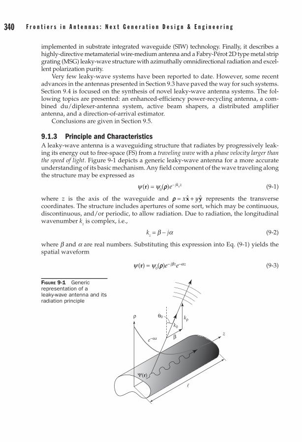
340 F r o n t i e r s i n a n t e n n a s : N e x t G e n e r a t i o n D e s i g n & e n g i n e e r i n g C h a p t e r 9 : L e a k y - W a v e a n t e n n a s 341
implemented in substrate integrated waveguide (SIW) technology. Finally, it describes a highly-directive metamaterial wire-medium antenna and a Fabry-Pérot 2D type metal strip grating (MSG) leaky-wave structure with azimuthally omnidirectional radiation and excel-lent polarization purity.
Very few leaky-wave systems have been reported to date. However, some recent advances in the antennas presented in Section 9.3 have paved the way for such systems. Section 9.4 is focused on the synthesis of novel leaky-wave antenna systems. The fol-lowing topics are presented: an enhanced-efficiency power-recycling antenna, a com-bined du/diplexer-antenna system, active beam shapers, a distributed amplifier antenna, and a direction-of-arrival estimator.
Conclusions are given in Section 9.5.
9.1.3 Principle and CharacteristicsA leaky-wave antenna is a waveguiding structure that radiates by progressively leak-ing its energy out to free-space (FS) from a traveling wave with a phase velocity larger than the speed of light. Figure 9-1 depicts a generic leaky-wave antenna for a more accurate understanding of its basic mechanism. Any field component of the wave traveling along the structure may be expressed as
y (r) = y0(r)e jk zz- (9-1)
where z is the axis of the waveguide and r = x yˆ ˆx y+ represents the transverse coordinates. The structure includes apertures of some sort, which may be continuous, discontinuous, and/or periodic, to allow radiation. Due to radiation, the longitudinal wavenumber kz is complex, i.e.,
kz = b - ja (9-2)
where b and a are real numbers. Substituting this expression into Eq. (9-1) yields the spatial waveform
y (r) = y0(r)e ej z z- -b a (9-3)
k0
kρ
e−αzz
Ψ(r)
β
θ0ρ
Figure 9-1 Generic representation of a leaky-wave antenna and its radiation principle

340 F r o n t i e r s i n a n t e n n a s : N e x t G e n e r a t i o n D e s i g n & e n g i n e e r i n g C h a p t e r 9 : L e a k y - W a v e a n t e n n a s 341
where b is the modal phase (propagation) constant and a is the leakage (attenuation) constant1. In general, both b and a are functions of frequency, and the functions b (w) and a (w) are called the dispersion and attenuation relations, respectively. In reality, b may represent either the dominant or higher-order mode of a uniform structure or a spatial harmonic of a periodic structure, as will be discussed later in this chapter.
From Maxwell’s equations and subsequent boundary conditions, the tangential part of the complex wavenumber vector k k= +ρ kzz is continuous at the interfaces with FS along the waveguide (WG) apertures. Therefore, we have [ ]( ) ( )k k kz z z
FS WGapertures= = .
Thus, the waveform in FS just above the structure exhibits the same z dependence as in Eq. (9-3). The fields outside the structure have the general form
ψ ψ ρρ b a( ) ( )r = - + -0e ej k z z (9-4)
where, from the wave equation and Eq. (9-2),
k k k k jzρ b a= - = - -02 2
02 2( ) . (9-5)
Assuming that a << b, which is a valid approximation in many practical antennas2, this relation reduces to k kρ b= -0
2 2 , and therefore kr is either purely real or purely imaginary. If b > k0 or, equivalently, if the phase velocity up = w/b is smaller than the speed of light in FS, vp < c = w/k0 (slow wave), then kr is imaginary and therefore the wave in the FS decays exponentially away from the structure; it is thus a purely guided wave. In contrast, if b < k0 or, equivalently, if vp > c (fast wave), then kr is real and therefore radiates into FS, with its main beam directed along the angle
q w b w b ww0
1
0
1( ) sin( )
sin( )=
=
- -k
c (9-6)
with respect to the normal of the structure3, as illustrated in Fig. 9-1. Other important parameters are the (main) beam width ∆q, the radiation efficiency er, and the tapered leakage factor function a(z) for a desired aperture profile function A(z), typically prescribed to minimize the sidelobe level, which are given by [3]
∆ ≈ ./
ql q
0 91
0 0( )cosl (9-7)
e er = - -1 2al (9-8)
1The time harmonic dependence exp(+jw t) is assumed throughout the chapter. Therefore, assuming a positive group velocity, the spatial variation exp(-j|b|z) represents a wave traveling toward the positive z direction (forward wave) while the spatial variation exp(+j|b|z) represents a wave traveling toward negative values of z (backward wave). In the case of a negative group velocity (typically corresponding to the case where the wave is launched toward the negative of z direction), the opposite is true.2Note that this condition automatically ensures that a << k0 because b is always smaller or at most of the order of k0 in leaky-wave antennas.3The operation of leaky-wave antennas is quite different from that of surface-wave antennas. Surface-wave antennas are also traveling-wave structures, but they use a guided (slow-wave) mode and therefore radiate mainly at the ends of the structure [6].
342 F r o n t i e r s i n a n t e n n a s : N e x t G e n e r a t i o n D e s i g n & e n g i n e e r i n g C h a p t e r 9 : L e a k y - W a v e a n t e n n a s 343
and
a( )( )
( ) ( )z
e A z
A z dz e A z dz
r
r
z=
/
-∫ ∫
2
02
02
2l
(9-9)
where l is the length of the antenna and l0 = 2p/k0 is the FS wavelength. In Eq. (9-7), the factor 0.91 for the numerator assumes a radiation efficiency of 90%, which is quite typical in leaky-wave antennas.
Many modern leaky-wave antennas are implemented in planar or quasi planar configurations. As apparent from Eq. (9-6), their main beam scans through space when fre-quency is varied if the fast-wave factor b(w)/k0 is frequency-dependent for a uniform structure4 or if it represents the space harmonic of a periodic structure. They may achieve very high directivity D Ae= /4 0
2p l (Ae: effective aperture) [7] for large antenna lengths l, as shown in Eq. (9-7), since their length can be increased independently of frequency, as long as power is left near the end of the structure [i.e., a is small enough so that 1 2 0- - >exp( )al ]. In contrast to array antennas, leaky-wave antennas do not require any complex feeding network; they are fed by a simple transmission line or wave-guide connection, while offering directivity and scanning performances sometimes comparable to those of arrays. Finally, they may radiate beams of different shapes. When its radiating aperture is narrow, a leaky-wave structure is approximately (Section 9.2) equivalent to a current source in the far-field, and it therefore radiates a beam in the form of a cone sharing its axis with that of the structure. If a ground plane is inserted below the antenna, a unidirectional fan beam may be achieved. Several 1D leaky-wave antennas can naturally be arrayed so as to form a 2D aperture and radiate a pencil beam, which may be steered by frequency tuning along the longitudinal planes and by phase-shifter tuning along the transverse planes [3].
9.1.4 ClassificationLeaky-wave antennas may be classified according to three categories—uniform, periodic and quasi-uniform—depending on their geometry and principle of operation [4]. They may also be 1D or 2D. This section focuses on 1D antennas. 2D leaky-wave antennas, which radiate a conical beam from a cylindrical traveling wave, are described in Section 9.2.
9.1.4.1 Uniform StructuresUniform leaky-wave antennas have a structure whose transverse cross-section is invariant under translation along the propagation axis. This axis corresponds to the longitudinal direction z in Fig. 9-1, and in all subsequent figures in this chapter. These antennas use the dominant mode or a higher-order fast-wave mode of the structure. Their phase constant is always positive and nonzero, i.e., b w( ) > 0 for all frequencies, since b e= k0 re with ere > 0, and therefore they are restricted to forward radiation,
4This may occur under two possible conditions (which may occur simultaneously). The first, which typically holds in uniform structures (Sec. 9.1.4.1), is when b (w) is a nonlinear function of frequency, i.e., when the structure is dispersive; in this case, b (w)/k0 = cb (w)/w varies with frequency and so does q0 according to Eq. (9-6). However, scanning may also be achieved when the structure is nondispersive, if the corresponding linear curve b (w) is shifted into the fast-wave region of the dispersion diagram, as in the case of the phase-reversal antenna presented in Section 9.3.2, where b e p/ ,= -re k p0 so thatb e p w/ /( )k c p0 = -re
varies with frequency.

342 F r o n t i e r s i n a n t e n n a s : N e x t G e n e r a t i o n D e s i g n & e n g i n e e r i n g C h a p t e r 9 : L e a k y - W a v e a n t e n n a s 343
excluding broadside5, according to the scanning law of Eq. (9-6). Two representative examples of uniform leaky-wave antennas are depicted in Fig. 9-2.
The uniform leaky-wave antenna shown in Fig. 9-2a is an empty rectangular wave-guide with a longitudinal radiating slit placed in the narrow wall of the waveguide [5]. In this antenna, the width of the slit is much narrower than the height b of the wave-guide, and therefore it causes only a small perturbation of the fast-wave TE10 dominant
mode with a phase constant b p10 0TE = - /k a , which is used by the antenna and whose
electric field (E) distribution is sketched in the figure. The baffle, when much larger than the wavelength, provides a regular conical-shaped fan beam in the radiation hemisphere, since the slit is then equivalent to a magnetic current source in FS, by image theory. The polarization of the antenna (direction of the radiated E field) is essentially azimuthal (i.e., in the j direction in spherical coordinates).
The uniform leaky-wave antenna shown in Fig. 9-2b is a microstrip transmission line structure. This antenna was invented by Menzel [8] and later explained by Oliner [9]. While the dominant quasi-TEM mode of a microstrip line is well-known to be a slow-wave (guided) mode, the higher-order EH1 of the structure is a fast-wave (radiating) mode and is therefore used by this antenna. The EH1 mode is an odd mode, as shown in the figure. A concern with this antenna is the suppression of the dominant even EH0 mode. This may be accomplished by placing shorting metal posts in the cen-ter of the structure between the strip and the ground plane. Another approach,
Waveguide
Baffle
RadiatingSlit
b
a
Free Space
Ex
y
z
(a)
Strip
DielectricSubstrate
Ground Plane
E
x
y
z
h
w
(b)
Figure 9-2 Examples of 1D uniform leaky-wave antennas. (a) Empty rectangular waveguide with a longitudinal slit in the narrow wall of the waveguide and with a ground plane baffle, operating in the weakly-perturbed TE
10 dominant mode [5]. (b) Wide microstrip line, operating in its first
higher-order mode (EH1) [8], [9].
5An exception would be for a structure excited at both of its ends or at its center, where the resulting waves, traveling in opposite directions (see Section 9.2.3), may combine their slightly symmetrically tilted beams to provide an overall broadside beam. However, this approach does not provide practical beam scanning since varying frequency would yield a pair of interdependent symmetric beams.
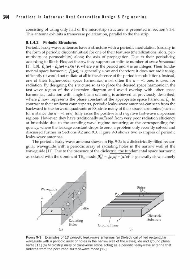
344 F r o n t i e r s i n a n t e n n a s : N e x t G e n e r a t i o n D e s i g n & e n g i n e e r i n g C h a p t e r 9 : L e a k y - W a v e a n t e n n a s 345
consisting of using only half of the microstrip structure, is presented in Section 9.3.6. This antenna exhibits a transverse polarization, parallel to the the strip.
9.1.4.2 Periodic StructuresPeriodic leaky-wave antennas have a structure with a periodic modulation (usually in the form of periodic discontinuities) for one of their features (metallizations, slots, per-mittivity, or permeability) along the axis of propagation. Due to their periodicity, according to Bloch-Floquet theory, they support an infinite number of space harmonics [1], [10], b w b w pn n p( ) ( )= + /0 2 , where p is the period and n is an integer. Their funda-mental space harmonic, b w0( ), is generally slow and therefore it does not radiate sig-nificantly (it would not radiate at all in the absence of the periodic modulation). Instead, one of their higher-order space harmonics, most often the n = -1 one, is used for radiation. By designing the structure so as to place the desired space harmonic in the fast-wave region of the dispersion diagram and avoid overlap with other space harmonics, radiation with single beam scanning is achieved as previously described, where b now represents the phase constant of the appropriate space harmonic bn. In contrast to their uniform counterparts, periodic leaky-wave antennas can scan from the backward to the forward quadrants of FS, since many of their space harmonics (such as for instance the n = -1 one) fully cross the positive and negative fast-wave dispersion regions. However, they have traditionally suffered from very poor radiation efficiency at broadside due to the standing-wave regime occurring at the corresponding fre-quency, where the leakage constant drops to zero, a problem only recently solved and discussed further in Sections 9.2 and 9.3. Figure 9-3 shows two examples of periodic leaky-wave antennas.
The periodic leaky-wave antenna shown in Fig. 9-3a is a dielectrically-filled rectan-gular waveguide with a periodic array of radiating holes in the narrow wall of the waveguide [11]. Due to the presence of the dielectric, the fundamental space harmonic associated with the dominant TE10 mode b e p10 0
2 2TE = - /rk a( ) is generally slow, namely
Figure 9-3 Examples of 1D periodic leaky-wave antennas (a) Dielectrically-filled rectangular waveguide with a periodic array of holes in the narrow wall of the waveguide and ground plane baffle [11] (b) Microstrip array of transverse strips acting as a periodic leaky-wave antenna that radiates from the perturbed surface-wave mode [12].
Waveguide
Baffle
RadiatingHoles
p
εrx
y
z
(a)
Strips
DielectricSubstrate
Ground Plane
p
xy
z
(b)

344 F r o n t i e r s i n a n t e n n a s : N e x t G e n e r a t i o n D e s i g n & e n g i n e e r i n g C h a p t e r 9 : L e a k y - W a v e a n t e n n a s 345
when e pr ak> + /1 20
2( ) , and the fast space harmonic most often used for radiation is n = -1. The periodic perturbation may be very significant and therefore strongly alter the nature of the aperiodic waveguide mode if the holes are large enough. This antenna exhibits radiation properties similar to those of the uniform antenna of Fig. 9-2a, except for its additional backward radiation capability.
The periodic leaky-wave antenna shown in Fig. 9-3b, is a microstrip array of trans-verse strips radiates in the perturbed TM0 surface-wave mode of the grounded slab. Although the structure has a unique axis of periodicity and a unique corresponding scanning plane, it may have an electrically large transverse aperture, and thereby radiate a pencil beam.
9.1.4.3 Quasi-Uniform StructuresQuasi-uniform leaky-wave antennas are topologically similar to periodic antennas and electromagnetically similar to uniform antennas. They exhibit a periodic structure, like the antennas shown in Fig. 9-3, but their period is much smaller than the guided wave-length of the traveling wave, p << lg, so that their higher-order space harmonics radiate at frequencies that are shifted well outside the frequency range of operation. Their dominant mode or, more precisely, their fundamental space harmonic (n = 0), which is the only significant one, must therefore necessarily be of fast-wave nature to provide radiation. For instance, the holey waveguide antenna shown in Fig. 9-3a with sub-wavelength spacing between the holes becomes a quasi-uniform antenna radiating from the fundamental space harmonic of the perturbed TE10 waveguide mode, pro-vided the permittivity is low enough so that the TE10 waveguide mode is a fast wave. Another example is the microstrip array structure of Fig. 9-3b, already discussed in the previous section but operating now as a perturbation of the first higher-order parallel-plate waveguide mode TE10 [12]. The CRLH antenna presented in Section 9.3.1 also belongs to this category and also radiates in its fundamental space harmonic, but unlike other quasi-uniform antennas is also capable of full-space scanning.
9.2 Theory of Leaky Waves9.2.1 Physics of Leaky-WavesIn this section, the basic physical properties of leaky waves on uniform (or quasi- uniform) and periodic guiding structures is studied. An understanding of the physical properties is important in order to understand the basic mechanism of leaky-wave antenna operation, and to understand phenomena such as the open stopband, which plagues conventional periodic leaky-wave antennas and prohibits scanning through broadside. (Several novel designs to overcome the stopband problem are presented in Section 9-3.)
As noted in Section 9.1, a leaky-wave antenna is a structure that supports a “leaky mode,” which is a guided mode that leaks, or radiates power, as it propagates on the guiding structure [1]–[4], [13]. For a uniform or quasi-uniform structure, the guided mode consists of a single wave that is a fast wave, having a complex wavenumber kz = b - ja, with the phase constant b in the range 0 < b < k0. For a periodic type of leaky-wave antenna with period p, the guided mode consists of an infinite number of space-harmonic waves, with wavenumbers kzn = bn - ja, where b b pn n p= + /0 2 (n an

346 F r o n t i e r s i n a n t e n n a s : N e x t G e n e r a t i o n D e s i g n & e n g i n e e r i n g C h a p t e r 9 : L e a k y - W a v e a n t e n n a s 347
integer) [1]. The n = 0 space harmonic, which carries most of the power, is referred to as the “fundamental” one, while the n = -1 space harmonic is usually the one that radi-ates, with -k0 < b-1 < k0. The main difference between the two types of structures is that the phase constant b-1 for the periodic structure may be either in the forward range (b-1 > 0) or in the backward range ( b-1 < 0). This allows for a beam that can point in either the forward or the backward quadrants of space, respectively, as opposed to a beam that can only point in the forward direction for the uniform or quasi-uniform structure6. In principle, the beam produced by a periodic leaky-wave antenna can point at broadside, though this requires special consideration, since broadside radiation cor-responds to operation near b-1 = 0, which corresponds to a type of stopband called the “open stopband” on the structure, discussed in more detail in Section 9.2.4. This stop-band usually prohibits the antenna from scanning in a stable fashion through broad-side, unless special designs are used that overcome the stopband problem. This has been the subject of much recent research, and is discussed in Section 9.3.
The beam angle is related to the phase constant by Eq. (9-6), where the phase con-stant denotes the phase constant of the radiating leaky wave, representing either the phase constant of the single leaky wave for a uniform structure, the phase constant of the fundamental space harmonic for a quasi-uniform structure, or the phase constant of the n = -1 space harmonic for a periodic leaky-wave antenna. In either case, it is assumed that power is flowing down the structure in the positive z direction, and hence a > 0. This normally implies that the group velocity (which is the same for all space harmonics) in the z direction is positive. For the periodic leaky-wave antenna the n = -1 space harmonic is called a forward wave if b-1 > 0, since the corresponding phase velocity in the z direction is positive and hence the phase and group velocities both have the same sign. If b-1 < 0, the phase velocity of this space harmonic is nega-tive, and hence opposite to the group velocity, so the space harmonic is called a back-ward wave [1].
Leaky-wave antennas may be approximately modeled as a traveling-wave source, where a current travels along the z-axis in free space (Fig. 9-1). (For those antennas hav-ing a ground plane as in Fig. 9-2, the source model is obtained after applying image theory, and hence gives the correct fields only in the region of space above the ground plane, where the radiation field exists.) The current may be either an electric current or a magnetic current, depending on the type of leaky-wave antenna being modeled. For aperture-type antennas, such as those in Figs. 9-2 and 9-3, a magnetic current is the most appropriate, since an aperture electric field is related to a magnetic surface cur-rent as M n Es = - ׈ [14]. For example, the uniform leaky-wave antennas in Fig. 9-2 can be approximately modeled as a magnetic line source with z-directed magnetic current flowing along the z-axis.
To be general, consider a magnetic current in FS in the form of a wave traveling along the entire z-axis, having the mathematical form
M p( ) ˆ ( ) ( )x y z x y e jk zz, , = -δ δ (9-10)
6Exceptions are the CRLH leaky-wave antenna (Section 9.3.1) and the ferrite waveguide antenna (Section 9.3.3), which both scan the entire spatial region despite their respective quasi-uniform and uniform natures.

346 F r o n t i e r s i n a n t e n n a s : N e x t G e n e r a t i o n D e s i g n & e n g i n e e r i n g C h a p t e r 9 : L e a k y - W a v e a n t e n n a s 347
where kz = b - ja and ˆ ˆp x= , y or z indicates the direction of the magnetic current. Note that for all the antennas in Figs. 9-2 and 9-3, the polarization (direction of the radiated electric field in the aperture) is y-directed. The fields from the magnetic current may be constructed from the electric vector potential as [14]
E F= - ∇ × .1
0e (9-11)
In this expression, F is the electric vector potential, which is given for the traveling-wave source in Eq. (9-10) by
F p=
ˆ ( )( )eρρ
002
4 jH k (9-12)
where H02( )( ). denotes the Hankel function of the second kind, and the radial wavenum-
ber is given by
k k kzρ = -( ) ./
02 2 1 2
(9-13)
The field produced by this infinite line source is in the form of a cone of radiation making an angle q0 with respect to the z-axis, as shown in Fig. 9-4 (which shows a mag-netic current flowing in the z direction). In particular, the Poynting vector is in the direction of the b vector, where b = Re(k), with the complex wavenumber vector k given by k z= +ˆ ˆk kz ρ ρ . Hence, we have that tan q0 = br/bz = Re(kr)/Re(kz). A forward wave radiates in the forward direction ( )0 20< < /q p while a backward wave radiates in the backward direction ( )p q p/ < <2 0 . When the structure is of finite length, the cone of radiation becomes a far-field beam of the antenna, as shown in Fig. 9-4. A broadside beam will be produced when b = 0.
One interesting aspect of the leaky-wave field arises from the choice of the square root in Eq. (9-13). There are two choices of the square root, mathematically correspond-ing to the fact that the radial wavenumber kr is a double-valued function of the complex
Figure 9-4 Illustration of the radiation produced by a traveling-wave source along the z-axis. Three cases are shown: a forward beam, a broadside beam, and a backward beam.
Forward beam
Broadside beam
Backward beam
z
Mθ0

348 F r o n t i e r s i n a n t e n n a s : N e x t G e n e r a t i o n D e s i g n & e n g i n e e r i n g C h a p t e r 9 : L e a k y - W a v e a n t e n n a s 349
variable kz. If the choice of the square root is made so that Im(kr ) < 0, the field will be exponentially decaying in the radial direction, and the field is termed “proper.” If the square root is chosen so that Im(kr ) > 0, the field is exponentially increasing in the radial direction, and the field is termed “improper” [4].
One might initially think that the “proper” choice is always the correct one, but this is not the case. To understand why, consider the case where 0 < b < k0. A ray picture for this case is shown in Fig. 9-5a, illustrated for the dielectric-filled holey waveguide in Fig. 9-3a, where spacing between the arrows signifies the magnitude of the time-average Poynting vector (a closer spacing corresponds to a larger power flow) and the direction of the arrows give the direction of power flow. Because of the attenuation constant a, less radiation comes from the structure as z increases. As can easily be seen from the dashed line in Fig. 9-5a, if one probes the field radially outward, the field is exponen-tially increasing. The radial wavenumber kr has a positive real part and a positive imaginary part, meaning that power is flowing radially outward (as expected) but the field is also increasing in the radial direction. The field is thus improper. The “proper” choice of the square root would give a field that decays radially, but has power flow radially inward. This is the type of wave that would correspond to a surface wave (a slow wave with b > k0) that decays in the z direction due to material loss. A leaky wave, however, which is a radiating type of wave, has an improper field when 0 < b < k0.
For a backward fast wave, the wavenumber lies in the range -k0 < b < 0, and the situation changes, with the ray picture shown in Fig. 9-5b. Now the field is proper in the radial direction [4]. Power flows outward radially, and the field also decays expo-nentially in the radial direction.
If the wave is a slow wave, with b > k0, then the wave has the character of a surface wave, and the field is exponentially decreasing, regardless of whether the wave is for-ward or backward. Table 9-1 summarizes the nature of the wave, depending on the value of the phase constant. The choice shown in Tab. 9-1 is called the “physical choice,” the choice that gives the correct physical behavior.
Figure 9-5 Illustration of radiation emanating from a dielectric-filled holey waveguide. (a) Radiation in the forward direction (improper wave). (b) Radiation in the backward direction (proper wave).
Power flow: β Power flow: β
Region of exp. growth
Input AbsorberLeaky mode Leaky mode
z
x
(a)
Region of exp. decay
Input Absorberkz = β − jα Waveguidekz = β − jα Waveguide
z
z
x
(b)
Table 9-1 Proper/Improper Nature of a Guided Wave
Forward (b > 0) Backward (b < 0)
Fast (|b| < k0) improper proper
Slow (|b| > k0) proper proper
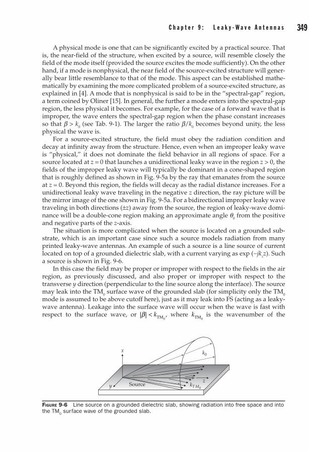
348 F r o n t i e r s i n a n t e n n a s : N e x t G e n e r a t i o n D e s i g n & e n g i n e e r i n g C h a p t e r 9 : L e a k y - W a v e a n t e n n a s 349
A physical mode is one that can be significantly excited by a practical source. That is, the near-field of the structure, when excited by a source, will resemble closely the field of the mode itself (provided the source excites the mode sufficiently). On the other hand, if a mode is nonphysical, the near field of the source-excited structure will gener-ally bear little resemblance to that of the mode. This aspect can be established mathe-matically by examining the more complicated problem of a source-excited structure, as explained in [4]. A mode that is nonphysical is said to be in the “spectral-gap” region, a term coined by Oliner [15]. In general, the further a mode enters into the spectral-gap region, the less physical it becomes. For example, for the case of a forward wave that is improper, the wave enters the spectral-gap region when the phase constant increases so that b > k0 (see Tab. 9-1). The larger the ratio b/k0 becomes beyond unity, the less physical the wave is.
For a source-excited structure, the field must obey the radiation condition and decay at infinity away from the structure. Hence, even when an improper leaky wave is “physical,” it does not dominate the field behavior in all regions of space. For a source located at z = 0 that launches a unidirectional leaky wave in the region z > 0, the fields of the improper leaky wave will typically be dominant in a cone-shaped region that is roughly defined as shown in Fig. 9-5a by the ray that emanates from the source at z = 0. Beyond this region, the fields will decay as the radial distance increases. For a unidirectional leaky wave traveling in the negative z direction, the ray picture will be the mirror image of the one shown in Fig. 9-5a. For a bidirectional improper leaky wave traveling in both directions (±z) away from the source, the region of leaky-wave domi-nance will be a double-cone region making an approximate angle q0 from the positive and negative parts of the z-axis.
The situation is more complicated when the source is located on a grounded sub-strate, which is an important case since such a source models radiation from many printed leaky-wave antennas. An example of such a source is a line source of current located on top of a grounded dielectric slab, with a current varying as exp (-jkzz). Such a source is shown in Fig. 9-6.
In this case the field may be proper or improper with respect to the fields in the air region, as previously discussed, and also proper or improper with respect to the transverse y direction (perpendicular to the line source along the interface). The source may leak into the TM0 surface wave of the grounded slab (for simplicity only the TM0 mode is assumed to be above cutoff here), just as it may leak into FS (acting as a leaky-wave antenna). Leakage into the surface wave will occur when the wave is fast with respect to the surface wave, or | | <b kTM0
, where kTM0 is the wavenumber of the
Source
x
yz
k0
kT M0
Figure 9-6 Line source on a grounded dielectric slab, showing radiation into free space and into the TM
0 surface wave of the grounded slab.

350 F r o n t i e r s i n a n t e n n a s : N e x t G e n e r a t i o n D e s i g n & e n g i n e e r i n g C h a p t e r 9 : L e a k y - W a v e a n t e n n a s 351
surface wave. The field will be improper in the y direction along the interface provided the wave is a forward wave that is fast with respect to the surface wave. The properties summarized in Tab. 9-1 remain valid for the nature of the surface-wave field produced by the line source, provided we interpret proper/improper as meaning in the trans-verse y direction, and fast/slow as meaning with respect to the wavenumber of the surface wave.
9.2.2 Radiation from 1D Unidirectional Leaky-WavesA unidirectional leaky wave is one that travels in a single direction (the z-direction) from an input (at z = 0) to an output (z = l). This corresponds to a leaky-wave antenna being operated in the usual fashion, with a feed at one end and a load at the other end. Consider the magnetic current source described by Eq. (9-10), with a magnetic current pointing in the p direction and flowing along the z-axis in FS in the region 0 < <z l. The far-field electric vector potential ψ = Fp is given by [16]
ψ ep
q=
-- +∫0 0
00
4e
re e dz
jk rjk z jk zz
l cos (9-14)
where q is the angle measured from the z-axis. The integral in Eq. (9-14), denoted as the array factor (AF ), may be evaluated in closed form as
AF e k kj k kz
z= -
- - /lll( cos ) ( cos )0 2
0 2q qsinc (9-15)
where sinc(x) = sin x/x. As the length l of the radiating source tends to infinity, the array factor reduces to the simpler form
AFj
k kz
= --
.0 cosq
(9-16)
This result clearly shows that the far-field pattern is in the form of a conical beam, with a maximum at some angle q0 from the z-axis. Based on this simpler array factor, the location of the beam maximum and the beam width of the pattern may be determined. From the above result, the exact value of the beam maximum (predicted by the array factor) is given by
cosq b0 0= /k (9-17)
which is the same as Eq. (9-6) except for a change in the angle definition. Equation (9-17) is exact for a unidirectional wave on an infinitely long structure. Note that for b > 0, as is the case for a uniform or a quasi-uniform leaky-wave antenna, the beam maxi-mum is never exactly at broadside. The pattern beam width, defined by the angle difference (in radians) between the two -3 dB points, is given approximately by
∆ = /q a q2 0 0( )csc ,k (9-18)
which assumes an infinite aperture as opposed to Eq. (9-7) which assumes a finite aper-ture and a 90% radiation efficiency. Note that because of the csc q0 term in Eq. (9-18), it becomes difficult to obtain narrow beams near the horizon (q0 ≈ 0). Physically, this is because the effective “projected aperture length” varies as sinq0.

350 F r o n t i e r s i n a n t e n n a s : N e x t G e n e r a t i o n D e s i g n & e n g i n e e r i n g C h a p t e r 9 : L e a k y - W a v e a n t e n n a s 351
9.2.3 Radiation from 1D Bidirectional Leaky-WavesA bidirectional leaky wave is one that travels equally in both directions (the ± z direc-tions) from a feed at z = 0 to the ends of the structure at z = ± /l 2. Assuming a magnetic current source as in Eq. (9-10), the line source is now described by
M p( ) ( ) ( )x y z x y e jk zz, , = .- | |δ δ (9-19)
This type of excitation normally produces a pair of conical beams, one pointing at q = q0 and one pointing at q = p - q0. Although this would normally be undesirable, an inter-esting case arises when q0 approaches p /2, and the two beams approach each other. In this case the two beams may merge into a single beam, which has a maximum at broad-side. In this way, a broadside beam can be produced by a leaky-wave antenna, when it is fed at the center. This is the practical motivation for considering a bidirectional leaky wave.
The far-field electric vector potential ψ = Fp , given by Eq. (9-14) for the unidirec-tional case, is modified to become for the bidirectional case
ψ ep
=
-
- /
+ / - | | +∫0 2
200
4e
re e
jk rjk z jk zz
l
l coosq dz. (9-20)
The integral in Eq. (9-20), denoted again as the array factor AF, may be evaluated in closed form as
AF jk e k k jkz
jkz
z
= -- / +- /
222
0 0l lcos( cos ) cos siq q nn( cos )
( cos )
k
k kz
02
02
2l qq
/ -
. (9-21)
For the case of an infinite aperture, l → ∞, the array factor simplifies to
AFjk
k kz
z
=-
-.
22
02( cos )q
(9-22)
After some simple calculus, the location of the beam maximum is found to be
cos ( ) ( )20 0
20
2q b a= / - / .k k (9-23)
In the limit as a / →k0 0, this result reduces to the simpler one shown in Eq. (9-17). For the case a << b, Eq. (9-17) is usually accurate enough to be used for a bidirectional wave. For beams pointing near broadside (q p0 2≈ / ), it is often the case that a and b are of comparable size, and hence Eq. (9-23) should be used.
Equation (9-23) predicts that the pattern will consist of a pair of conical beams, point-ing at q p δq= / ±2 , for some δq , when b a> . When b a< , the right-hand side of Eq. (9-23) is negative. In this case the beam has a maximum at q p= /2, i.e., at broadside. Hence, for a bidirectional leaky wave, the point b = a is a beam splitting point. For b > a there will be two distinct maxima, and hence a split beam. For b >> a the split beam will be essen-tially two distinct beams with little overlap. On the other hand, for b < a, there will be a single beam (a fan beam) pointing at broadside (see Fig. 9-4). Figure 9-7 shows the varia-tion in the shape of the conical beam as b increases relative to a, illustrating how the beam evolves from a broadside fan beam to a pair of conical beams.

352 F r o n t i e r s i n a n t e n n a s : N e x t G e n e r a t i o n D e s i g n & e n g i n e e r i n g C h a p t e r 9 : L e a k y - W a v e a n t e n n a s 353
For the case of a scanned beam, where b >> a, the formula for the beam width is the same as for the unidirectional case, Eq. (9-18). For a broadside beam with b ≤ a, the -3 dB beam width formula (the angle in radians between the two -3 dB points) is [17]
∆ = - + - +q b a b a b a2 2 42 2 22 2 2 2( ) (9-24)
where b b= /k0 and a a= /k0. The beam radiated by a bidirectional leaky wave will always point at broadside for
b < a. If b and a are viewed as independent parameters, then for a given value of a, the broadside beam will become narrower as the value of b decreases, becoming the nar-rowest for the case of b = 0, corresponding to an aperture that is everywhere in phase. (This means physically that the radiation from each point along the aperture will add in phase in the broadside direction.) However, in many practical leaky-wave antennas there is a relationship between b and a, determined by the structure. In this case, the narrowest possible broadside beam will in general occur at a particular frequency, depending on the structure. Many leaky-wave antennas fall into the general category of a guiding structure that consists of a waveguide (e.g., a parallel-plate waveguide or a rectangular waveguide) that has a radiating aperture on one face of the waveguide. The antennas shown in Fig. 9-2 are examples of this. Such structures can be modeled as a waveguiding region that is terminated with a “partially reflecting surface” or PRS, modeled as a shunt susceptance Bs. The transverse equivalent network (TEN) transmis-sion line model for such a structure is shown in Fig. 9-8. For example, the transmission line of length h in Fig. 9-8 would model the width a of the rectangular waveguide in the leaky-wave antenna shown in Fig. 9-2a. For structures in this category, it has been shown that near broadside, the relationship between b and a is approximately described by the hyperbolic relationship [17]
ba = ,constant (9-25)
and the narrowest broadside beam will occur at the frequency for which [17]
b a/ = - = . .3 1
20 518 (9-26)
If it is assumed that the TEN model is excited with a fixed amplitude parallel cur-rent generator as shown in Fig. 9-8, then the power density radiated in the broadside direction by the antenna is maximized at the frequency corresponding to [17]
b a= . (9-27)
Figure 9-7 Sketch showing how the radiation pattern of a bidirectional wave varies as the phase constant changes relative to the attenuation constant
β < α β > α
β >> α
z

352 F r o n t i e r s i n a n t e n n a s : N e x t G e n e r a t i o n D e s i g n & e n g i n e e r i n g C h a p t e r 9 : L e a k y - W a v e a n t e n n a s 353
This type of excitation would correspond, for example, to a y-directed coaxial probe feed extending between the top and bottom walls of the rectangular waveguide in Fig. 9-2a. The beam width when operating at the maximum power density point [Eq. (9-27)] is larger than that at the minimum beam width point [Eq. (9-26)] by a factor of 2 1 189211 4/ = . [17]. At the point of maximum broadside power density (b = a), the beam width formula in Eq. (9-24) simplifies to
∆ = / .q a2 2 0( )k (9-28)
9.2.4 Radiation from Periodic StructuresAs noted in Section 9.1, a periodic leaky-wave antenna consists of a slow-wave struc-ture that has been modified by periodically modulating the structure in some fashion. A typical example is the microstrip combline structure shown in Fig. 9-9, consisting of a microstrip line with a periodic set of radiating stubs attached.
Because of the periodicity, the modal field of the periodically-loaded structure is now in the form of a space-harmonic or Floquet-wave expansion [1] and may be written as
E A( ) ( )x y z x y en
njk z, , = ,
=-∞
+∞-∑ zn (9-29)
where
k kn
pzzn = +02p (9-30)
is the wavenumber of the nth space harmonic (n an integer) and p is the period. The zero space harmonic with wavenumber k jz0 0= -b a is usually defined as the wave that approaches the mode of the unperturbed waveguide when the loading (the stub
Figure 9-8 Transverse equivalent network model for a leaky-wave antenna that consists of a waveguide that has a partially reflecting surface (PRS) on one face. The parallel current source I
s
models a feed in the actual structure.
h
x
Z0Z0 Is jBs
z
y p
SubstrateMicrostrip line
Radiating stubs
Figure 9-9 Microstrip combline leaky-wave antenna (top view)

354 F r o n t i e r s i n a n t e n n a s : N e x t G e n e r a t i o n D e s i g n & e n g i n e e r i n g C h a p t e r 9 : L e a k y - W a v e a n t e n n a s 355
length in Fig. 9-9) tends to zero. It is then customary to denote b = b0. The normalized phase constant of the nth space harmonic is b b ln k k n p/ = / + /0 0 0 0 .
Leakage (radiation per-unit-length of the structure) will occur provided one of the space harmonics (usually the n = -1 space harmonic) is a fast wave, so that - < <-k k0 1 0b . The normalized phase constant of the n = -1 space harmonic is
b b l- / = / - / .1 0 0 0 0k k p (9-31)
By choosing the period p appropriately, the beam can be aimed from backward end-fire to forward end-fire. The beam will automatically scan as the frequency changes, since the right-hand side of Eq. (9-31) usually increases with frequency. If one wishes to have single-beam scanning over the entire range from backward end-fire to forward end-fire, the n = -2 space harmonic must remain a slow backward wave (b-2 < -k0) while the fundamental n = 0 space harmonic must remain a slow forward wave (b0 > k0) as the -1 space harmonic is scanned from backward to forward end-fire. This requires the constraint that ere > 9 [3], where ere is the effective relative permittivity of the quasi-TEM microstrip mode. It is also required that p/ < /l0 1 2 at the highest (forward end-fire) frequency.
One difficulty encountered in the scanning of periodic leaky-wave antennas such as the combline structure is that the beam shape degrades as the beam is scanned through broadside. This is because the broadside operating point b-1 = 0 corresponds to b0 p = 2p. This point is called an “open stopband” of the periodic structure, because it corresponds to a stopband appearing on an open structure, for which one of the space harmonics (n = -1) is radiating. At the open stopband frequency, all reflections from the radiating stub discontinuities in Fig. 9-9 add in phase back to the source. At this point a perfect standing wave is set up within each unit cell of the structure [1] and the attenuation constant drops to zero.
To understand the open stopband physically, consider the equivalent circuit of the combline structure, which is shown in Fig. 9-10. The transmission line represents the fundamental mode of the microstrip line, having a characteristic impedance Z0, and the shunt impedances Zs representing the active impedances of the stubs. (The active stub impedance is the impedance of a stub when radiating in the periodic environ-ment. This is the same as the impedance of a single stub only if mutual coupling between stubs is neglected.)
When the broadside point is reached, all of the stubs are excited in phase with b-1 = 0, or equivalently b0 p = 2p. Therefore, the stub admittances Ys = 1/Zs all add together in phase. The result is a short-circuit condition at the location of each stub. The field within the unit cell between adjacent stubs thus becomes a perfect standing wave, and not a traveling wave. There is no radiation at this point, since the voltage at each stub drops to zero. The attenuation constant of the leaky mode drops to zero when this
Figure 9-10 Equivalent circuit of the combline structure
p
Z0Z0 ZsZsZs ZsZs

354 F r o n t i e r s i n a n t e n n a s : N e x t G e n e r a t i o n D e s i g n & e n g i n e e r i n g C h a p t e r 9 : L e a k y - W a v e a n t e n n a s 355
point is reached. For an infinitely long structure, the input impedance at the stub loca-tion would be a short circuit, and hence no power could be delivered to the antenna. In practice, for a finite-length structure, the input match would degrade as the beam is scanned through broadside. The beamwidth would also change significantly as the beam is scanned through broadside, dropping exactly to zero at the stopband point b-1 = 0 for an infinite structure. The topic of eliminating or at least reducing the open stopband effect is a very important one, since this is the main limitation for achieving a continuous scanning from the backward to the forward quadrants with a single antenna. This is discussed is Section 9.2.5, and Section 9.3 is partly devoted to explor-ing different leaky-wave antennas that overcome the open stopband problem.
When designing, analyzing, and interpreting results for periodic leaky-wave anten-nas, a useful tool is the Brillouin diagram [1], [10], [18], [19]. This is a plot of k 0 p versus bn p, plotted on the type of diagram that is shown in Fig. 9-11. On this diagram each space harmonic n will have a plot that is shifted from the adjacent ones, n - 1 and n + 1, by 2p. Hence, the diagram is periodic with a period of 2p. The thick solid lines on the diagram indicate boundaries k0 = ±b where a space harmonic (usually the n = -1 space harmonic) will be radiating at backward end-fire or forward end-fire. Between these two lines is the radiation region, where the space harmonic will be a fast wave, and hence a radiating wave. The shaded regions (the regions that are inside the lower tri-angles) are the bound-wave (nonradiating) regions [1], [18], [19]. If any space harmonic lies within one of these triangles at the frequency of interest, then all of the space har-monics will lie within these triangles at this frequency, and hence they will all be slow (and hence nonradiating) waves. The overall mode is then a mode that does not radi-ate, i.e., a surface-wave type of mode. For a point outside the bound-wave (shaded) triangles, there must be at least one space harmonic that lies within the radiation region, and hence the overall mode is a leaky mode. One immediate consequence of the Brillouin diagram is that if the frequency is high enough so that k0 p > p, the guided mode must be a leaky mode, since all the space harmonic points must then lie above the shaded triangles.
A wavenumber plot for a typical combline structure is shown in Fig. 9-12 [20]. Exactly at the stopband point, b-1 p = 0 and a = 0, and a short circuit appears at opposite
Figure 9-11 Brillouin diagram for a periodic structure, showing the radiation (fast-wave) region and the bound-mode (shaded) region for which all space harmonics are slow waves. The diagonal lines with labels give the dispersion plot for the space harmonics of a TEM air-filled structure.
βnp
k0p
−2π −π 0 +π +2π
2π
−4π −3π +3π +4π
4π
Radiation region
n = +
1n = +1
n = 0
n = 0 n = −
1n = −1 n = −
2 n = −2
n = −3n = −
3
3π
π
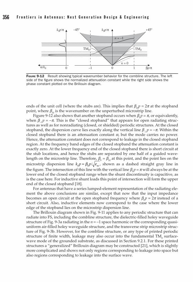
356 F r o n t i e r s i n a n t e n n a s : N e x t G e n e r a t i o n D e s i g n & e n g i n e e r i n g C h a p t e r 9 : L e a k y - W a v e a n t e n n a s 357
ends of the unit cell (where the stubs are). This implies that bMp = 2p at the stopband point, where bM is the wavenumber on the unperturbed microstrip line.
Figure 9-12 also shows that another stopband occurs when b0 p = p, or equivalently, when b-1 p = -p. This is the “closed stopband” that appears for open radiating struc-tures as well as for nonradiating (closed, or shielded) periodic structures. At the closed stopband, the dispersion curve lies exactly along the vertical line b-1 p = -p. Within the closed stopband there is an attenuation constant a, but the mode carries no power. Hence, the attenuation constant does not correspond to leakage in the closed stopband region. At the frequency band edges of the closed stopband the attenuation constant is exactly zero. At the lower frequency end of the closed stopband there is short circuit at the stub locations, and hence the stubs are separated by one half of a guided wave-length on the microstrip line. Therefore, b0 = bM at this point, and the point lies on the microstrip dispersion line k p p0 0= /b ere , shown as a dashed straight gray line in the figure. The intersection of this line with the vertical line b0 p = p will always be at the lower end of the closed stopband range when the shunt discontinuity is capacitive, as is the case here. For inductive shunt loads this point of intersection will form the upper end of the closed stopband [18].
For antennas that have a series lumped-element representation of the radiating ele-ment the above conclusions are similar, except that now that the input impedance becomes an open circuit at the open stopband frequency where b0 p = 2p instead of a short circuit. Also, inductive elements now correspond to the case where the lower edge of the stopband lies on the microstrip dispersion line.
The Brillouin diagram shown in Fig. 9-11 applies to any periodic structure that can radiate into FS, including the combline structure, the dielectric-filled holey waveguide structure of Fig. 9-3a radiating in the n = -1 space harmonic or the corresponding quasi-uniform air-filled holey waveguide structure, and the transverse strip microstrip struc-ture of Fig. 9-3b. However, for the combline structure, or any type of printed periodic structure of finite width, leakage may also occur into the fundamental TM0 surface-wave mode of the grounded substrate, as discussed in Section 9.2.1. For these printed structures a “generalized” Brillouin diagram may be constructed [21], which is slightly more complicated and shows not only regions corresponding to leakage into space but also regions corresponding to leakage into the surface wave.
Figure 9-12 Result showing typical wavenumber behavior for the combline structure. The left side of the figure shows the normalized attenuation constant while the right side shows the phase constant plotted on the Brillouin diagram.
α/k0 βp/π
k0p/π
n = 0
n = –1
+45º–45º
TM0 TM0
k0p/π
0 0–1 1

356 F r o n t i e r s i n a n t e n n a s : N e x t G e n e r a t i o n D e s i g n & e n g i n e e r i n g C h a p t e r 9 : L e a k y - W a v e a n t e n n a s 357
9.2.5 Broadside Radiation9.2.5.1 Scanning Through BroadsideAs noted in Section 9.2.4, the combline structure, which has the equivalent circuit shown in Fig. 9-10, cannot radiate directly at broadside as a leaky-wave antenna. Similarly, any periodic leaky-wave antenna structure having an equivalent circuit con-sisting of pure shunt or series elements on a transmission line cannot radiate at broadside. In order to be able to scan through broadside, the equivalent circuit of the radiating element within the unit cell must be something more complicated than a pure series or shunt element; i.e., it must have the form of a T or II network. In Section 9.3 examples of periodic leaky-wave antennas that overcome the stopband problem at broadside will be given, and it will be seen that all of them have a more complicated unit cell than a simple series or shunt radiating element. An example is the quarter-wave transformer design discussed there.
One case of particular interest is the case of an artificial or metamaterial transmis-sion line that supports a fast wave. The CRLH metamaterial leaky-wave antenna is a novel example of this [22], [23]. Consider a unit cell of such a structure that has the network model shown in Fig. 9-13, consisting of a series element with an impedance Zse = Rse + jXse and a shunt element with an admittance Ysh = Gsh + jBsh. From transmission-line theory [24], the wavenumber of the transmission-line mode that propagates on this structure is given by
kjp
Z Yz = - .se sh (9-32)
Squaring both sides of the above equation and separating the real and imaginary parts leads to the following two equations:
b a2 22
1- = - -p
R G X B( ),se sh se sh (9-33a)
212ab = - .
pX G R B( )se sh se sh (9-33b)
At the stopband frequency corresponding to broadside radiation, b = 0. Assuming this condition, combining the above two equations, and solving for a, we have
a = +
.1 2
pR G
RG
Bse shse
shsh (9-34)
Zse
Ysh
pFigure 9-13 Unit cell of an artificial transmission line, showing the series and shunt impedance elements

358 F r o n t i e r s i n a n t e n n a s : N e x t G e n e r a t i o n D e s i g n & e n g i n e e r i n g C h a p t e r 9 : L e a k y - W a v e a n t e n n a s 359
This result shows that if only one of the two elements in Fig. 9-13 has a real part, and hence corresponds to a radiating element, it is not possible to have a finite nonzero value of a at the broadside frequency. In order for the right-hand side of the above equation to remain nonzero and finite, we need to have both Rse > 0 and Gsh > 0. The CRLH structure discussed in Section 9.3.1 fulfills this requirement.
9.2.5.2 Fixed-Beam Broadside RadiationIf one does not require scanning through broadside, but merely the creation of a broad-side beam at a single frequency, this may be realized by using either a uniform (or quasi-uniform) or a periodic type of leaky-wave antenna. For the periodic leaky-wave antenna, a broadside beam may be produced if the structure is fed at one end (as is usually the case with a leaky-wave antenna) and the structure is designed to overcome the stopband limitation, as previously discussed and illustrated with examples in Section 9.3. In this case the structure is not only capable of radiating at boradside, but at other angles as well, as the frequency changes.
Alternatively, a finite-length periodic leaky-wave antenna may be operated exactly at the stopband point corresponding to b-1 = 0, or equivalently, b0 p = 2p, which means that all radiating unit cells of the antenna structure are exactly in phase. In this case the finite-length leaky-wave antenna is operating as a standing-wave antenna, and the input impedance and beamwidth depend directly on the length of the structure. Waveguide-fed slot arrays are examples of antennas in this category [25]. Another example is the combline structure operating as a standing-wave antenna array, shown in Fig. 9-14. (Figure 9-14 shows a combline structure fed at one end, although it is also possible to feed the antenna at the center.)
If a single stub is modeled as a parallel admittance Ys connected to the microstrip line, the input admittance at the beginning of the structure is then Yin = NYs, where N is the number of stubs. This impedance can be matched to the feeding line using a suit-able matching circuit at the input, as shown in Fig. 9-14. The beamwidth for this struc-ture is inversely related to the antenna length as for any uniform linear array, namely ∆ = . / /q l0 89 0( )l , where l = -( )N g1 l is the total antenna length.
It is interesting to observe the limit as N becomes large, tending to infinity. This limit represents the combline antenna acting as an infinite leaky-wave antenna, operat-ing exactly at the stopband point. In this limit the input impedance tends to zero, mean-ing that no power can be delivered to the antenna. Also, the beamwidth tends to zero. This is consistent with the fact that the attenuation constant is zero exactly at the stop-band frequency, with the stubs in all unit cells then having equal-amplitude excitation. At this frequency there is a perfect standing wave within each unit cell, with a short circuit at either end of the unit cell (where a stub is), and no power flows along
Figure 9-14 Combline structure operating as a standing-wave antenna. The structure is terminated with a short circuit at the end, l
g /4 from the last stub.
p = λg
InputSubstrate
Microstrip line
Radiating stubsλg/4 TransformerShortcircuit
λg/4
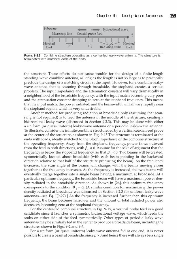
358 F r o n t i e r s i n a n t e n n a s : N e x t G e n e r a t i o n D e s i g n & e n g i n e e r i n g C h a p t e r 9 : L e a k y - W a v e a n t e n n a s 359
the structure. These effects do not cause trouble for the design of a finite-length standing-wave combline antenna, as long as the length is not so large as to practically preclude the design of a matching circuit at the input. However, for a combline leaky-wave antenna that is scanning through broadside, the stopband creates a serious problem. The input impedance and the attenuation constant will vary dramatically in a neighborhood of the broadside frequency, with the input match becoming very poor and the attenuation constant dropping to zero at the stopband frequency. This means that the input match, the power radiated, and the beamwidth will all vary rapidly near the stopband region, which is very undesirable.
Another method for producing radiation at broadside only (assuming that scan-ning is not required) is to feed the antenna in the middle of the structure, creating a bidirectional leaky wave (discussed in Section 9.2.3). This may be done with either a uniform (or quasi-uniform) leaky-wave antenna or a periodic leaky-wave antenna. To illustrate, consider the infinite combline structure fed by a vertical coaxial feed probe at the center of the structure, as shown in Fig. 9-15.The structure is terminated at the ends with loads, ideally matched to the Bloch impedance of the combline structure at the operating frequency. Away from the stopband frequency, power flows outward from the feed in both directions, with b-1 ≠ 0. Assume for the sake of argument that the frequency is below the stopband frequency, so that b-1 < 0. Two beams will be created, symmetrically located about broadside (with each beam pointing in the backward direction relative to that half of the structure producing the beam). As the frequency increases, the scan angle of the beams will change, with the beams moving closer together as the frequency increases. As the frequency is increased, the two beams will eventually merge together into a single beam having a maximum at broadside. At a particular optimum frequency, the broadside beam will have a maximum power den-sity radiated in the broadside direction. As shown in [26], this optimum frequency corresponds to the condition b-1 = a. (A similar condition for maximizing the power density radiated at broadside was discussed in Section 9.2.3 for uniform leaky-wave antennas—see Eq. [(9-27).] As the frequency is increased further than this optimum frequency, the beam becomes narrower and the amount of total radiated power also decreases, becoming zero at the stopband frequency.
For the center-fed combline structure in Fig. 9-15, a vertical probe feed is a good candidate since it launches a symmetric bidirectional voltage wave, which feeds the stubs on either side of the feed symmetrically. Other types of periodic leaky-wave antennas may be similarly fed in the center to produce a broadside beam, including the structures shown in Figs. 9-2 and 9-3.
For a uniform (or quasi-uniform) leaky-wave antenna fed at one end, it is never possible to create a beam at broadside, since b > 0 and hence there will always be a single
Figure 9-15 Combline structure operating as a center-fed leaky-wave antenna. The structure is terminated with matched loads at the ends.
z
yp
Substrate
Microstrip line
Radiating stubs
Coaxial probe feedBidirectional wave
Matchedload
Matchedload

360 F r o n t i e r s i n a n t e n n a s : N e x t G e n e r a t i o n D e s i g n & e n g i n e e r i n g C h a p t e r 9 : L e a k y - W a v e a n t e n n a s 361
beam pointing at some angle in the forward quadrant, determined by the value of b in accordance with Eq. (9-17). However, by feeding the structure in the middle, an opti-mum broadside beam can be achieved, just as in the periodic case, with the optimum condition for maximum power density radiated at broadside being b = a [17]. As noted in Section 9.2.3, this result applies to any uniform or quasi-uniform leaky-wave antenna that is based on a waveguiding structure having a radiating face that can be modeled as a partially reflecting surface, which is modeled as a sheet impedance in the trans-verse equivalent network model of the structure. The holey waveguide and the Menzel (microstrip EH1) leaky-wave antennas shown in Fig. 9-2 fall into this category.
9.2.6 Radiation from 2D Leaky-WavesA two-dimensional (2D) leaky wave is one that propagates radially outward from a source along a planar interface as shown in Fig. 9-16. The leaky wave then establishes an aperture distribution on the interface that produces a beam of radiation that may be conical in shape, with a beam angle q0 defined about the vertical z-axis in Fig. 9-16, or a narrow pencil beam radiated at broadside (q0 = 0 in Fig. 9-16). The beams are illustrated in Fig. 9-17. As is true for all leaky-wave antennas, the beam angle is frequency sensitive.
Figure 9-16 Geometry of a two-dimensional (2D) radially-propagating leaky wave. The leaky wave propagates outward radially along the guiding structure, as depicted by the arrows.
x
y
z
Source
Guiding structure
Figure 9-17 Illustration of the types of beams that may be produced with a 2D radial leaky-wave antenna. (a) Conical beam. (b) Broadside beam. A vertical dipole source can only produce a conical beam, while a horizontal dipole source (shown in the figure) may produce either type of beam.
Beam Beam
Source Source
(a) (b)
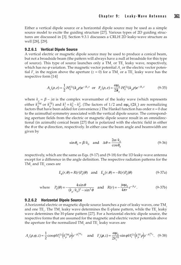
360 F r o n t i e r s i n a n t e n n a s : N e x t G e n e r a t i o n D e s i g n & e n g i n e e r i n g C h a p t e r 9 : L e a k y - W a v e a n t e n n a s 361
Either a vertical dipole source or a horizontal dipole source may be used as a simple source model to excite the guiding structure [27]. Various types of 2D guiding struc-tures are discussed in [3]. Section 9.3.1 discusses a CRLH 2D leaky-wave structure as well [28], [29].
9.2.6.1 Vertical Dipole SourceA vertical electric or magnetic dipole source may be used to produce a conical beam, but not a broadside beam (the pattern will always have a null at broadside for this type of source). This type of source launches only a TMz or TEz leaky wave, respectively, which has no j variation. The magnetic vector potential Az or the electric vector poten-tial Fz in the region above the aperture (z = 0) for a TMz or a TEz leaky wave has the respective form [14]
A z H k e F zzjk z
zz( ) ( ) ( )( )ρ ρ ρ
wmρ, = , =-1
2 202 0or
kkH k e
z
jk zz02( )( )ρρ - (9-35)
where kr = b - ja is the complex wavenumber of the leaky wave (which represents either kρ
TM or kρTE) and k k kz
202 2= - ρ. (The factors of 1/2 and wm0 2/( )kz are normalizing
factors that have been added for convenience.) The Hankel function has order n = 0 due to the azimuthal symmetry associated with the vertical dipole source. The correspond-ing aperture fields from the electric or magnetic dipole source result in an omnidirec-tional (in azimuth) conical beam [27] that is polarized with the electric field in either the q or the j direction, respectively. In either case the beam angle and beamwidth are given by
sincos
q b qa
q0 00
0
2= / ∆ =
/k
kand (9-36)
respectively, which are the same as Eqs. (9-17) and (9-18) for the 1D leaky-wave antenna except for a difference in the angle definition. The respective radiation patterns for the TMz and TEz cases are
E r R r P E r R r Pq jq q q q( ) ( ) ( ) ( ) ( ) ( ), = , = -0 0and (9-37a)
where Pk k
R rj
re0
02 2
044
( )sin
( ) sin( )q q
qwmpρ
= -/ -
= -and -- .jk r0 (9-37b)
9.2.6.2 Horizontal Dipole SourceA horizontal electric or magnetic dipole source launches a pair of leaky waves, one TMz and one TEz. The TMz leaky wave determines the E-plane pattern, while the TEz leaky wave determines the H-plane pattern [27]. For a horizontal electric dipole source, the respective forms that are assumed for the magnetic and electric vector potentials above the aperture for the normalized TMz and TEz leaky waves are
A z H k e Fzjk z
zz( ) cos (( )ρ j j ρρ, , = ( ) -1
2 12 TM TM
and ρρwm
j ρρ, = ( ) .-zk
H k ez
jk zz) sin ( )012
2 TETE TE
(9-38)

362 F r o n t i e r s i n a n t e n n a s : N e x t G e n e r a t i o n D e s i g n & e n g i n e e r i n g C h a p t e r 9 : L e a k y - W a v e a n t e n n a s 363
The corresponding respective radiation patterns for the TMz and TEz cases are
E r R r P E r R rq jq j q j q q j( ) ( )cos cos ( ) ( ) ( ), , = , , , = -1 ssin ( )j qC , (9-39a)
E r R r P E r R rj qq j j q q j q( ) ( )sin ( ) ( ) ( )cos, , = - , , , =1 ccos ( )j qC (9-39b)
where andPj
k
jk
k kC
j1 2
02 2
2 4 2( )
sin( )q
ρ
ρ
ρ= -
-= -
kkρ= .constant (9-39c)
In these expressions kr once again denotes either kρTM or kρ
TE. In order to have a narrow pencil beam at broadside, a necessary condition is that A k B k/ = /ρ ρ
TM TE [27], where A and B are the (complex) amplitudes of the TMz and TEz leaky waves, respectively (defined with respect to the normalization used in Eqs. (9-38). The beamwidths in the E and H planes are then given by the same expression as in (9-36) for the n = 0 leaky wave, so that
∆ =/
∆ =/
.qa
aqE H
k k2 20
0
0
0
TM TEandcos cos
(9-40)
Assuming that aTM = bTM and aTE = bTE (see the discussion in Section 9.2.3), the beam-widths in the E plane (j = 0) and H plane (j = p/2) will then be [27]
∆ = ∆ = .q a q aE H2 2 2 2TM TEand (9-41)
In order to have a symmetric pencil beam at broadside (having equal beamwidths in the E and H planes), one must have k kρ ρ
TE TM≈ .
9.3 Novel Structures9.3.1 Full-Space Scanning CRLH AntennaComposite right/left-handed (CRLH) metamaterials [23] are transmission-line type metamaterial structures of one, two, or three dimensions, whose propagation along a given direction can generally be modeled by the periodic unit cell shown in Fig. 9-18a. Figure 9-18b shows a microstrip implementation of a 1D CRLH structure. The size of the unit cell, or period p, must be much smaller than the guided-wavelength ( p << lg) so that, in the frequency range of interest, the structure behaves as an effectively homogeneous—or uniform—transmission line structure. The unit cell model of Fig. 9-18a includes the left-handed (LH) series capacitance CL and shunt inductance LL as well as the right-handed (RH) series inductance LR and shunt capacitance CR. Its immittances (impedance Z and admittance Y ) are
Z R j LC
R jCR
L L
p g= + -
= +/ - /
→→w
ww w
wl1 12( )se 00
′Z p, (9-42a)
Y G j CL
G jLR
L L
p g= + -
= +/ - /
→→
ww
w ww
l1 12( )sh 00′ ,Y p (9-42b)
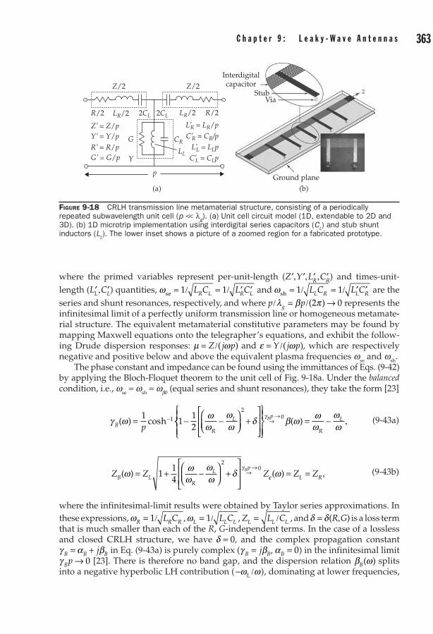
362 F r o n t i e r s i n a n t e n n a s : N e x t G e n e r a t i o n D e s i g n & e n g i n e e r i n g C h a p t e r 9 : L e a k y - W a v e a n t e n n a s 363
where the primed variables represent per-unit-length ( ′, ′, ′ , ′Z Y L CR R) and times-unit-length ( ′ , ′L CL L) quantities, wse = / = / ′ ′1 1L C L CR L R L and wsh = / = / ′ ′1 1L C L CL R L R are the series and shunt resonances, respectively, and where p pg/ = / →l b p( )2 0 represents the infinitesimal limit of a perfectly uniform transmission line or homogeneous metamate-rial structure. The equivalent metamaterial constitutive parameters may be found by mapping Maxwell equations onto the telegrapher’s equations, and exhibit the follow-ing Drude dispersion responses: m w= /Z j p( ) and e w= /Y j p( ), which are respectively negative and positive below and above the equivalent plasma frequencies wse and wsh.
The phase constant and impedance can be found using the immittances of Eqs. (9-42) by applying the Bloch-Floquet theorem to the unit cell of Fig. 9-18a. Under the balanced condition, i.e., wse = wsh = wb0 (equal series and shunt resonances), they take the form [23]
g w ww
ww
δBR
L
p( ) cosh= - -
+
-1
112
1
2
= - ,→
→gb w w
www
Bp
R
L0 ( ) (9-43a)
Z Z ZB LR
LpB( )w w
www
δg
= + -
+
→→
114
20
cc L RZ Z( )w = = , (9-43b)
where the infinitesimal-limit results were obtained by Taylor series approximations. In these expressions, wR R RL C= /1 , wL L LL C= /1 , Z L CL L L= / , and δ δ= ,( )R G is a loss term that is much smaller than each of the R, G-independent terms. In the case of a lossless and closed CRLH structure, we have δ = 0, and the complex propagation constant g a bB B Bj= + in Eq. (9-43a) is purely complex (g bB Bj= , aB = 0) in the infinitesimal limit g Bp → 0 [23]. There is therefore no band gap, and the dispersion relation b wB( ) splits into a negative hyperbolic LH contribution (- /w wL ), dominating at lower frequencies,
Figure 9-18 CRLH transmission line metamaterial structure, consisting of a periodically repeated subwavelength unit cell (p << l
g). (a) Unit cell circuit model (1D, extendable to 2D and
3D). (b) 1D microtrip implementation using interdigital series capacitors (CL) and stub shunt
inductors (LL). The lower inset shows a picture of a zoomed region for a fabricated prototype.
Z/2
Z’ = Z/p L’R = LR/pC’R = CR/p
L’L = LLpC’L = CLp
Y’ = Y/pR’ = R/pG’ = G/p
Z/2
R/2 LR/2 LR/2
CR
LL
2CL 2CL
G
Y
p
R/2
Interdigitalcapacitor
StubVia
Ground plane(a) (b)
z

364 F r o n t i e r s i n a n t e n n a s : N e x t G e n e r a t i o n D e s i g n & e n g i n e e r i n g C h a p t e r 9 : L e a k y - W a v e a n t e n n a s 365
and a positive linear RH contribution (+ /w wR), dominating at higher frequencies.7 When the structure is open to FS, as required for an antenna behavior, radiation loss exist and may be modelled by R and G [30], leading to δ ≠ 0, and a propagation con-stant bB which may be rewritten k jz = -b a , where a now represents leakage. More-over, the characteristic impedance is independent of frequency (ZC = ZL = ZR), and therefore allows broadband matching to a constant impedance (generally 50Ω) port. The (band-pass) dispersion relation and Bloch impedance given by Eq. (9-43) are plot-ted in Figs. 9-19a and 9-19b, respectively.8
As a consequence of the CRLH dispersion characteristic (Fig. 9-19(a)), according to the scanning law of Eq. (9-6), a CRLH leaky-wave antenna scans the entire spatial region from q = - °90 to q = + °90 , as frequency is varied from w b= - c to w b= + c, includ-ing q = 0° at wb0 (where vg = ∂ /∂ ≠w b 0), as shown in Fig. 9-19c. The leakage constant,
Figure 9-19 Typical response of a balanced (wse
= wsh
) transmission line CRLH metamaterial structure. (a) Bloch dispersion relation g
B(w) [Eq. (9-43a)]. (b) Bloch impedance Z
B(w)
[Eq. (9-43b)]. (c) Leaky-wave scanning law q(w) = sin-1[bB(w)/k
0]. Dissipation loss is
neglected everywhere. The CRLH structure is a band-pass type filter, with the RH low-pass and LH high-pass stopbands indicated in (a).
0123456789
101112
0 0γBp = (α + jβ)p
Freq
uenc
y(G
Hz)
−π +πβ < 0(LH) β > 0(RH)
Radiation
Guidance
Guidance
ωBF
ωBWD
ωcR
ωEF
ωFWDωβ0
LH HP stop band
RH LP stopband
α
α
β
β = + k0
β = −k0
ωcL
(a) Dispersion relation
0 1
RB
XB
XB
(b) Impedance
−90 0 +90θ (deg)
(c) Scanning law
ZBZ0
RB + jXBZ0
=
7When the balance condition is not satisfied (i.e., w wse sh≠ ), the propagation constant g B is either purely imaginary (g bB j= , pass-band) or purely real (g aB j= , pass-band), and a stopband occurs at the transition frequency between the LH and RH ranges, preventing broadside radiation.8Since the structure is periodic, its fields, in complete rigor, must be expressed as an expansion over an infinite number of space harmonics [Eq. (9-29)], which may be written in 1D as b w b w pm m p( ) ( )= ± + / 0 2 [10], and the dispersion diagram periodically extends to ±∞ along bp, beyond the first Brillouin zone following the space harmonics shown in Fig. 9-11, with bp and k0p periods of 2p. In the Bragg regime, where p is on the order of lg/2 or larger, Bragg-like scattering (unit cell resonance) occurs and several space harmonics significantly contribute to the fields. In contrast, in the metamaterial regime, which occurs in the balanced CRLH case at the frequency wb0, the contribution of non-zero space harmonics is typically negligible, so that only the fundamental space harmonic b w b w( ) ( )= 0 produces a significant contribution, and the refractive index may be defined in terms of this fundamental space harmonic as n k c( ) ( ) ( )w b w b w w= / = /0 0 0
.
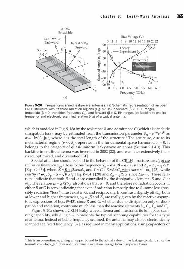
364 F r o n t i e r s i n a n t e n n a s : N e x t G e n e r a t i o n D e s i g n & e n g i n e e r i n g C h a p t e r 9 : L e a k y - W a v e a n t e n n a s 365
which is modeled in Fig. 9-18a by the resistance R and admittance G (which also include dissipation loss), may by estimated from the transmission parameter S e e j
21 = - -a bl l as a = - | | /ln( )S21 l, where l is the total length of the structure.9 The structure, due to its metamaterial regime (p << lg), operates in the fundamental space harmonic, n = 0. It belongs to the category of quasi-uniform leaky-wave antennas (Section 9.1.4.3). This backfire-to-endfire antenna was invented in 2002 [22], and was later extensively theo-rized, optimized, and diversified [31].
Special attention should be paid to the behavior of the CRLH structure exactly at the transition frequency wb 0. Close to this frequency, g a bB j ZY p= + ≈ / and Z Z Z YB c≈ = / [Eqs. (9-43)], where Z ≈ R + j2w∆wLR and Y ≈ G + j2w∆wCR with ∆w = w - wb 0 [23], while exactly at wb0
, g aB RG p= ≈ / [Eq. (9-34)] [20] and Z R GB = / since ∆w = 0. These rela-tions indicate that both b and a are controlled by the dissipative elements R and G at wb0. The relation a = /RG p also shows that a = 0, and therefore no radiation occurs, if either R or G is zero, indicating that even if radiation is mostly due to R, some loss (pos-sibly radiation “loss”) must exist in G, and reciprocally. In contrast, slightly off wb 0, both at lower and higher frequencies, g bB j= and ZB are really given by the reactive asymp-totic expressions of Eqs. (9-43), since R and G, whether due to dissipation only or dissi-pation and radiation, contribute much less than the reactive elements LR, CR, LL, and CL.
Figure 9-20a shows a CRLH leaky-wave antenna and illustrates its full-space scan-ning capability, while Fig. 9-20b presents the typical scanning capabilities for this type of antenna. Instead of being frequency scanned, the antenna may also be electronically scanned at a fixed frequency [32], as required in many applications, using capacitors or
Figure 9-20 Frequency-scanned leaky-wave antennas. (a) Schematic representation of an open CRLH structure with its three radiation regions (Fig. 9-19c): backward (b < 0, LH range), broadside (b = 0, transition frequency fb0
), and forward (b > 0, RH range). (b) Backfire-to-endfire frequency and electronic scanning relation q(w) of a typical antenna.
x
y
z
θSource
Backward
Broadside
Forward
ω0 < ω < ωEF
ωBF < ω < ω0
ω = ω0
AB
C
(a)
0
TheoryExperiment θ
Varactors
Frequency (GHz)3.0 3.5 4.0 4.5 5.0 5.5 6.0 6.5
Scan
ned
Ang
le θ
0 (d
eg)
A
B
C
fBF fEFf0
Bias Voltage (V)
x
(b)
22201816141210864290
60
30
0
–30
–60
–90
9This is an overestimate, giving an upper bound to the actual value of the leakage constant, since the formula a = - | |/ln S21 l does not discriminate radiation leakage from dissipative losses.

366 F r o n t i e r s i n a n t e n n a s : N e x t G e n e r a t i o n D e s i g n & e n g i n e e r i n g C h a p t e r 9 : L e a k y - W a v e a n t e n n a s 367
inductors controlled by a bias field. In this case, it is also possible to equalize the beam-width as the scan angle varies by using a nonuniform biasing distribution along the structure [32]. The antenna considered here is a 1D structure of the type shown in Fig. 9-18. Therefore, it provides scanning only in one plane. While the beam is very directive in this plane (xz in Fig. 9-20a), it is broad in the perpendicular plane (xy in Fig. 9-20a): this is a fan beam. This antenna was also used in a reflecto-directive system in [33]. A pencil beam can naturally be achieved by arraying several 1D structures in a conventional array configuration [31].
Because it is essentially “seen” as a uniform medium by electromagnetic waves, a 1D CRLH structure may be straightforwardly extended to 2D [28], [29]. This is illustrated in Fig. 9-21a. When excited in its center (e.g., by a coaxial probe), such a 2D CRLH structure supports a perfectly circular surface wave in its metamaterial regime. When this wave is of leaky nature, it radiates a conical beam, as depicted in Fig. 9-21a and demonstrated in Fig. 9-21b. As frequency varies, the opening angle of the conical pattern varies, following the dispersion relation Eq. (9-43a), which leads to beam scanning. Due to azimuthal symmetry, the LH and RH ranges provide the same functionality, but with opposite scanning slopes (dq0/dw).
9.3.2 Full-Space Scanning Phase-Reversal AntennaThe CRLH full-space scanning antennas presented in Section 9.3.1 are periodic leaky-wave structures that operate in the fundamental (n = 0) space harmonic due to the strongly subwavelength nature of the period (p << lg). This section presents a full-space scanning periodic phase-reversal leaky-wave antenna, with a non-subwavelength period (p ≈ lg/2 at broadside), which may be interpreted to operate either in the n = -1 space harmonic or in the n = 0 space harmonic due to inversion of the phase between the two conductors of the structure in each unit cell.
The first ever reported phase-reversal antenna was perhaps the Franklin antenna [34]. This is a p = lg/2 periodic wire structure loaded by lg/4 U-shaped wire sections which are oriented perpendicularly to the axis of the antenna and which shift the phase by 180° (i.e., reverse it) to ensure an in-phase current distribution along this axis for radiation. Recently, a uniplanar version of the phase-reversal antenna was reported in [35]. This antenna is implemented in offset parallel strip (OPS) technology. In contrast to the Franklin antenna, it radiates from the phase-reversing loads as opposed to the lg/2 sections of the structure. While this antenna, similarly to previous phase-reversal antennas, was terminated by a short circuit and was therefore resonant, allowing only fixed-beam radiation with p = lg/2, it may be terminated by a matched load, and thereby become a (traveling-wave) full-space scanning leaky-wave antenna [36], with some similarities to log-periodic type antennas [1].
The full-space scanning OPS phase-reversal leaky-wave antenna is depicted in Fig. 9-22 [36]. Figure 9-22a shows an overall view of the structure, which consists of alternating OPS transmission line sections and crossover strips. The latter locally invert the phases along the structure by cross-connecting the two conducting strips. The metal-lizations can be placed on the two sides of a thin substrate to avoid air bridges for the crossovers, as suggested by the dark and light strip representation in Fig. 9-22a. The OPS sections do not radiate, due to their oppositely directed (balanced) currents +I and -I on the two strips. In contrast, the crossover strips support transverse current components in the same directions, as shown in Fig. 9-22b, and therefore radiate, with an equivalent current intensity of 2 I cosx, as illustrated in Fig. 9-22c. This current corresponds to the

366 F r o n t i e r s i n a n t e n n a s : N e x t G e n e r a t i o n D e s i g n & e n g i n e e r i n g C h a p t e r 9 : L e a k y - W a v e a n t e n n a s 367
Figure 9-21 Conical-beam leaky-wave antenna. (a) Conical-beam leaky-wave radiation produced by a fast isotropic (metamaterial range) radial wave and three corresponding 2D CRLH mushroom-type [23] structures (top view): 1 simple mushroom structure, 2 interdigital mushroom structure, 3 Stepped-impedance balanced structure. (b) Radiation patterns and scanning law obtained with structure 1. The maximum LH and RH gains are 17.3 dB at 10.1 GHz and 12.4 dB at 11 GHz, respectively.
1 2 3
zθ (ω)
(a)
9 10 11 12 13 14 15 16 17 180
1020304050607080
MeasuredTheoretical
LH
–50–55
–30–35–40
–50
–55
–45
9090
45
0
45
9090
45
0
45
LH RH
9.0 GHz9.6 GHz10.1 GHz
11.0 GHz13.0 GHz15.0 GHz
Frequency (GHz)
Ang
le (d
eg)
(b)
GAP RH
–35–40
–45
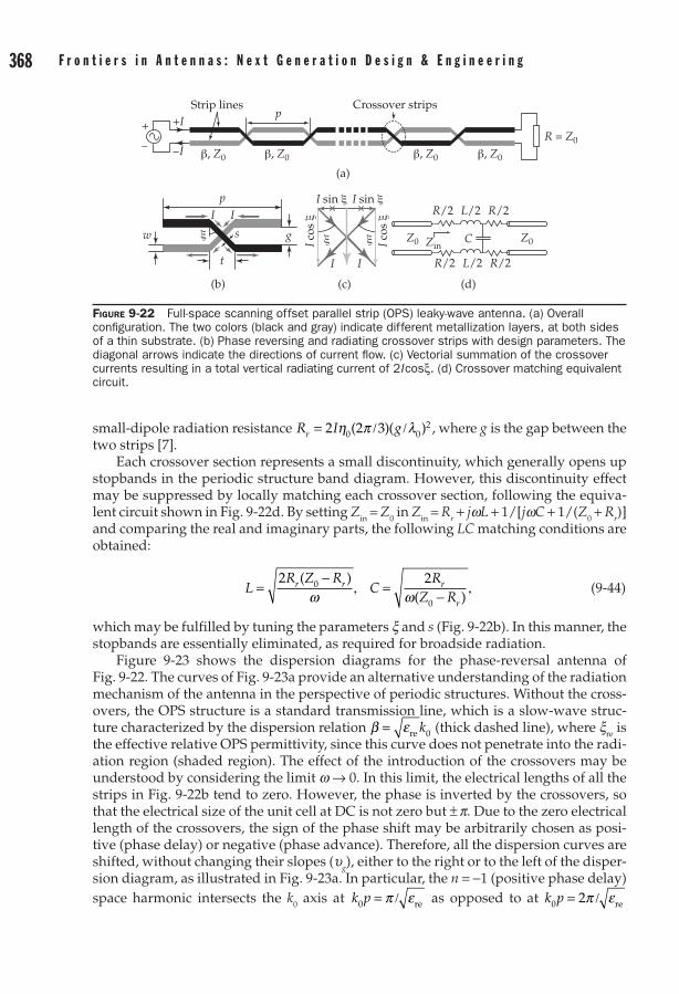
368 F r o n t i e r s i n a n t e n n a s : N e x t G e n e r a t i o n D e s i g n & e n g i n e e r i n g C h a p t e r 9 : L e a k y - W a v e a n t e n n a s 369
small-dipole radiation resistance R I gr = / /2 2 30 02η p l( )( ) , where g is the gap between the
two strips [7]. Each crossover section represents a small discontinuity, which generally opens up
stopbands in the periodic structure band diagram. However, this discontinuity effect may be suppressed by locally matching each crossover section, following the equiva-lent circuit shown in Fig. 9-22d. By setting Zin = Z0 in Zin = Rr + jwL + 1/[jwC + 1/(Z0 + Rr)] and comparing the real and imaginary parts, the following LC matching conditions are obtained:
LR Z R
CR
Z Rr r r
r
=-
, =-
,2 20
0
( )( )w w
(9-44)
which may be fulfilled by tuning the parameters x and s (Fig. 9-22b). In this manner, the stopbands are essentially eliminated, as required for broadside radiation.
Figure 9-23 shows the dispersion diagrams for the phase-reversal antenna of Fig. 9-22. The curves of Fig. 9-23a provide an alternative understanding of the radiation mechanism of the antenna in the perspective of periodic structures. Without the cross-overs, the OPS structure is a standard transmission line, which is a slow-wave struc-ture characterized by the dispersion relation b e= re k0 (thick dashed line), where xre is the effective relative OPS permittivity, since this curve does not penetrate into the radi-ation region (shaded region). The effect of the introduction of the crossovers may be understood by considering the limit w → 0. In this limit, the electrical lengths of all the strips in Fig. 9-22b tend to zero. However, the phase is inverted by the crossovers, so that the electrical size of the unit cell at DC is not zero but ± p. Due to the zero electrical length of the crossovers, the sign of the phase shift may be arbitrarily chosen as posi-tive (phase delay) or negative (phase advance). Therefore, all the dispersion curves are shifted, without changing their slopes (ug), either to the right or to the left of the disper-sion diagram, as illustrated in Fig. 9-23a. In particular, the n = -1 (positive phase delay) space harmonic intersects the k0 axis at k p0 = /p ere as opposed to at k p0 2= /p ere
Figure 9-22 Full-space scanning offset parallel strip (OPS) leaky-wave antenna. (a) Overall configuration. The two colors (black and gray) indicate different metallization layers, at both sides of a thin substrate. (b) Phase reversing and radiating crossover strips with design parameters. The diagonal arrows indicate the directions of current flow. (c) Vectorial summation of the crossover currents resulting in a total vertical radiating current of 2I cosx. (d) Crossover matching equivalent circuit.
+_
β, Z0 β, Z0 β, Z0β, Z0
Crossover strips+I
−I
p
R = Z0
Strip lines
(a)
sw gξ
p
t
(b)
II
III sin ξI sin ξ
I cos
ξ
I cos
ξ
(c)
Z0Z0
R/2R/2 L/2
R/2R/2 L/2
CZin
(d)
ξ ξ
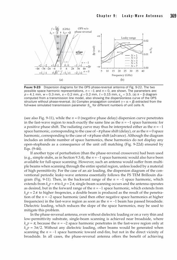
368 F r o n t i e r s i n a n t e n n a s : N e x t G e n e r a t i o n D e s i g n & e n g i n e e r i n g C h a p t e r 9 : L e a k y - W a v e a n t e n n a s 369
(see also Fig. 9-11), while the n = 0 (negative phase delay) dispersion curve penetrates in the fast-wave region to reach exactly the same line as the n = -1 space harmonic for a positive phase shift. The radiating curve may thus be interpreted either as the n = -1 space harmonic, corresponding to the case of -p phase shift (delay), or as the n = 0 space harmonic, corresponding to the case of +p phase shift (advance). Although the diagram includes an infinite number of space harmonics, these harmonics do not display any open-stopbands as a consequence of the unit cell matching (Fig. 9-22d) ensured by Eqs. (9-44).
If another type of perturbation (than the phase-reversal crossovers) had been used (e.g., simple stubs, as in Section 9.3.4), the n = -1 space harmonic would also have been available for full-space scanning. However, such an antenna would suffer from multi-ple beams when scanning through the entire spatial region, unless loaded by a material of high permittivity. For the case of an air loading, the dispersion diagram of the con-ventional periodic leaky-wave antenna essentially follows the FS TEM Brillouin dia-gram (Fig. 9-11). Then, in the backward range of the n = -1 space harmonic, which extends from k0 p = p to k0 p = 2 p, single-beam scanning occurs and the antenna operates as desired, but in the forward range of the n = -1 space harmonic, which extends from k0 p = 2 p to higher freqencies, a double beam is produced as the result of the penetra-tion of the n = -2 space harmonic (and then other negative space harmonics at higher frequencies) in the fast-wave region as soon as the n = -1 beam has passed broadside. Dielectric loading, which reduces the slope of the space harmonics, may be used to mitigate this problem.
In the phase-reversal antenna, even without dielectric loading or on a very thin and low-permittivity substrate, single-beam scanning is achieved near broadside, where k0 p = p, because the n = -2 space harmonic penetrates in the fast-wave region only at k0 p = 3p/2. Without any dielectric loading, other beams would be generated when scanning the n = -1 space harmonic toward end-fire, but not in the direct vicinity of broadside. In all cases, the phase-reversal antenna offers the benefit of achieving
Figure 9-23 Dispersion diagrams for the OPS phase-reversal antenna of Fig. 9-22. The two possible space harmonic representations, n = −1 and n = 0, are shown. The parameters are: p = 4.1 mm, w = 0.3 mm, s = 0.2 mm, g = 0.2 mm, t = 0.15 mm, e
re = 3.5. (a) k − b diagram
computed from a transmission line model, also showing the dispersionless curve of the OPS structure without phase-reversal. (b) Complex propagation constant g = a + jb extracted from the full-wave simulated transmission parameter S
21 for different numbers of unit cells N.
4π3π2ππ–π–2π–3π–4π 0
50
40
30
20
10
+10+2 +1 −1 0 −1−2
+1 +20+1 −1 0 −1 −2
f =k0c2π (GHz)
c2p εre
βp
k0 = −β k0= +βOPS w/o
phase reversal
n = −1
n = 0
(a)
0
0.02
0.01
0.005
N = 1N = 2N = 3N = 5N = 7
Leaky range
−π
+π
Frequency (GHz)
βp (r
ad)
α/k 0
(b)
40353025201510
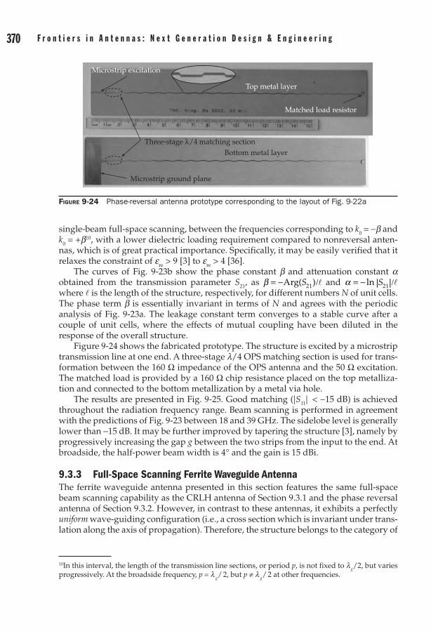
370 F r o n t i e r s i n a n t e n n a s : N e x t G e n e r a t i o n D e s i g n & e n g i n e e r i n g C h a p t e r 9 : L e a k y - W a v e a n t e n n a s 371
single-beam full-space scanning, between the frequencies corresponding to k0 = -b and k0 = +b10, with a lower dielectric loading requirement compared to nonreversal anten-nas, which is of great practical importance. Specifically, it may be easily verified that it relaxes the constraint of ere > 9 [3] to ere > 4 [36].
The curves of Fig. 9-23b show the phase constant b and attenuation constant a obtained from the transmission parameter S21, as b = - /Arg( )S21 l and a = - | |/ln S21 l where l is the length of the structure, respectively, for different numbers N of unit cells. The phase term b is essentially invariant in terms of N and agrees with the periodic analysis of Fig. 9-23a. The leakage constant term converges to a stable curve after a couple of unit cells, where the effects of mutual coupling have been diluted in the response of the overall structure.
Figure 9-24 shows the fabricated prototype. The structure is excited by a microstrip transmission line at one end. A three-stage l/4 OPS matching section is used for trans-formation between the 160 Ω impedance of the OPS antenna and the 50 Ω excitation. The matched load is provided by a 160 Ω chip resistance placed on the top metalliza-tion and connected to the bottom metallization by a metal via hole.
The results are presented in Fig. 9-25. Good matching (|S11| < -15 dB) is achieved throughout the radiation frequency range. Beam scanning is performed in agreement with the predictions of Fig. 9-23 between 18 and 39 GHz. The sidelobe level is generally lower than -15 dB. It may be further improved by tapering the structure [3], namely by progressively increasing the gap g between the two strips from the input to the end. At broadside, the half-power beam width is 4° and the gain is 15 dBi.
9.3.3 Full-Space Scanning Ferrite Waveguide AntennaThe ferrite waveguide antenna presented in this section features the same full-space beam scanning capability as the CRLH antenna of Section 9.3.1 and the phase reversal antenna of Section 9.3.2. However, in contrast to these antennas, it exhibits a perfectly uniform wave-guiding configuration (i.e., a cross section which is invariant under trans-lation along the axis of propagation). Therefore, the structure belongs to the category of
Figure 9-24 Phase-reversal antenna prototype corresponding to the layout of Fig. 9-22a
Top metal layer
Bottom metal layer
Microstrip excitation
Matched load resistor
Microstrip ground plane
Three-stage λ/4 matching section
10In this interval, the length of the transmission line sections, or period p, is not fixed to l g/2, but varies progressively. At the broadside frequency, p = l g/ 2, but p ≠ l g/ 2 at other frequencies.

370 F r o n t i e r s i n a n t e n n a s : N e x t G e n e r a t i o n D e s i g n & e n g i n e e r i n g C h a p t e r 9 : L e a k y - W a v e a n t e n n a s 371
uniform leaky-wave antennas. It does not support any space harmonics and is also much easier to design. It uses its dominant (lowest frequency) propagation mode for radiation, as will be shown.
The antenna structure is depicted in Fig. 9-26a and a corresponding prototype is shown in Fig. 9-26b. It consists of an open rectangular waveguide filled with a ferrite material biased perpendicularly to the large side. Although this structure is extremely simple and relatively similar to that of edge-mode isolators11, it was first demonstrated as a full-space scanning leaky-wave antenna only very recently [39].
Figure 9-25 Experimental results for the phase-reversal antenna of Fig. 9-24. (a) Reflection coefficient. (b) Radiation patterns at the selected frequencies: 18, 19.5, 20.5, 21.5, 22.5, 23.5, 24.5, 25, 27, 29, 31, 33, 35, 37, 39 GHz. The range of frequencies shown is limited to 18 to 39 GHz, due to the limitations of the horn antennas used for measurement (K and Ka bands), but actually extends beyond in reality.
Frequency (GHz)
S 11
(dB
)
Leaky range
(a)
18 GHz24.5 GHz
39 GHz
Angle of Radiation (deg)
(dB
)
(b)
0–5
–10–15–20–25–30–35–40
0
–10
–20
–30
–40
–50–900 10 20 30 40 –60 –30 0 30 60 90
11Usually, edge-mode isolators are not exactly configured as waveguides. Rather, they consist of a tapered T junction microstrip transmission line three-port network, where the transmit-direction power travels along the straight edge of the structure while the attenuation-direction power is routed at the junction toward the perpendicular port, where it is dissipated by an absorber [37] or by a shorting connection to the ground at the edge of the substrate [38]. The waveguide structure of Fig. 9-26a may be seen as the limiting case of the short-circuit edge-mode isolator where the shorting line length reduces to zero and where the substrate is cut off at the edge of the straight microstrip line.
Figure 9-26 Uniform ferrite-loaded open waveguide leaky-wave antenna. (a) Basic structure. (b) Prototype with a back conductor and stub matching network. The structure is 10 cm in length, which corresponds to about 2l
0 at broadside (fb,0
= 5.9 GHz).
H0
x
y
z
x = −w x = 0
∼PMC
PEC
PEC
Ferrite
Radiation
(a)
Matching sectionsNdFeB magnet
Waveguide structure (open side)(b)

372 F r o n t i e r s i n a n t e n n a s : N e x t G e n e r a t i o n D e s i g n & e n g i n e e r i n g C h a p t e r 9 : L e a k y - W a v e a n t e n n a s 373
The lowest modes of the structure of Fig. 9-26a are quasi-TE my
0 modes12 when the height of the waveguide is much smaller than its width [39]. These modes exhibit the following electric and magnetic field expressions:
E E k x ey xj z= ,-
0 sin( ) b (9-45a)
H jE
z
E
xH j
E
xxe
y yz
e
y=∂∂
-∂∂
, = -
∂∂
+1 1wm
κm wm
κκm
∂∂
,
E
zy (9-45b)
where the transverse wavenumber kx is related to the longitudinal wavenumber b by
k kx e= - = - .2 2 2 2b w em b (9-46)
In these relations, me is the bulk birefringent effective permeability
m m κm
mw w w
w w w wm
w we
m
m
p= - =- +
- +=
-2 2
0
20
2
20 0
0
2( )( )
22
2 2w w-,
r
(9-47)
where m and k are the traditional Polder tensor terms m m m m w w w w= = = + / -xx yy m0 0 02 21( ) ( )
and κ m m m ww w w= - = = / -xy yx m0 02 2( ), respectively, and where w w m w wp e m= = = +( )0 0
and w w m w w wr e m= = ∞ = +( ) ( )0 0 are the plasma and the resonance frequencies, respectively; furthermore, w gm0 0 0= H is the ferromagnetic resonance frequency and w gmm sM= 0 is the saturation frequency, where g is the gyromagnetic ratio, H0 is the applied magnetic bias field, and Ms is the saturation magnetization [40].
The dispersion relation of the structure, which may be easily derived by the trans-verse resonance technique, takes the form of the transcendental equation [41]13
F k wk
jkx
x
e
x
( ) cot( )b w bκm
wmη
, = + - = .0
0 (9-48)
The first two modes of the corresponding dispersion diagram are plotted in Fig. 9-27 for typical ferrite and waveguide parameters. The dominant mode is a balanced CRLH type of mode that exhibits four characteristic dispersion regions (LH-guided, LH-leaky, RH-leaky, an RH-guided), while the second mode is the classical edge mode which is of no interest here.
Compared to the CRLH metamaterial-type dispersion (Section 9.3.1), the CRLH dis-persion characteristic of the ferrite waveguide antenna exhibits the following distinct features: (i) its LH and RH bands are not related to double negative and double positive effective parameters e and m (see Fig. 9-27), but to the specific anisotropic waveguide
12These modes are exactly TEy in the limit where the permittivity of the ferrite tends to infinity, since then E Ex f x a r f, , ,= / →e 0, where the subscripts f and a refer to the ferrite and air regions, respectively. In this case, the ferrite-air interface is equivalent for TEy modes to a perfect magnetic conductor (PMC), where radiation is considered as a second-order effect, justified by the fact that the leakage constant is generally very small, a/k0 << 1. In practice, er,f ≈ 15, and the PMC approximation is therefore generally acceptable for relatively small waveguide heights. 13In the PMC limit 1 0/erf → , or for very small waveguide widths, the last term of F( )b w, , which accounts for the opening of the waveguide to FS, may be ignored to a good approximation in the dispersion relation.

372 F r o n t i e r s i n a n t e n n a s : N e x t G e n e r a t i o n D e s i g n & e n g i n e e r i n g C h a p t e r 9 : L e a k y - W a v e a n t e n n a s 373
structure of the antenna; (ii) the dispersion is automatically “balanced,” i.e., never exhibits any stopbands between the LH and RH branches of the CRLH mode, which greatly simplifies the design; (iii) due to the gyrotropy of the ferrite, the response is nonreciprocal, i.e., no negative slope (∂ /∂ = <w b vg 0)14 curve exists, a characteristic which will be exploited in the combined du/diplexer-antenna of Section 9.4.2. The dispersion behavior of Fig. 9-27 was confirmed by full-wave and experimental results in [39], which also includes an approximate formula for the transition frequency fb 0, a paramet-ric study for the existence of a balanced CRLH type of mode, and a computation of the leakage constant (a / ≈ .k0 0 3 in the prototype demonstrated).
Figure 9-28 shows time-snapshots of the vectorial electric field distribution in the LH range, at fb 0, and in the RH range. In contrast to the case of metamaterial-type CRLH structures, where the fields distributions are quite diffuse and vectorially com-plex with local longitudinal components, this ferrite structure, due to its uniformity, exhibits perfectly clear LH and RH triads (E, Ht, b) (Ht: transverse magnetic field). The attenuation of the wave observed in Fig. 9-28 is due to a combination of radiation leak-age and ferrite dissipation. As in other balanced and matched CRLH structures, the wave has a traveling wave (as opposed to standing wave) nature even at the transition frequency15 since vp(fb 0) ≠ 0 (Fig. 9-27).
In the far-field, the structure of Fig. 9-26a is seen as a current line supporting a CRLH-type current. Consequently, the antenna radiates a conical beam (see Fig. 9-4) with an axis coinciding with the axis of the waveguide (z direction). The far-field
14Such a curve, existing in many ferrite structures (see for instance the related CRLH dual-band ferrite waveguide leaky-wave antenna reported in [42]), would not correspond to propagation of energy or information toward the source, which would be noncausal (in a relatively low-loss and nondispersive frequency range), but simply to a mode allowed to propagate only in the direction opposite to the one indicated by the curve in Fig. 9-27b. 15This may be verified by computing the Poynting vector S = E × H, which is nonzero and pointing toward the +y direction through the scanning range, including at fb 0.
Figure 9-27 Dispersion diagram for the structure of Fig. 9-26a computed by Eq. (9-48) for typical YIG ferrite and waveguide parameters, indicated in the inset of (a). (a) Frequency range from 4 to 10 GHz. (b) Magnification of the CRLH range around the LH-RH transition frequency fb 0
, from 5.5 to 6.5 GHz. The sign of the phase velocity, u
p = w/b, varies across the CRLH-like dispersion range
[up(fb 0
) < 0, up(fb 0
) = 0 and up (fb 0
) > 0], while the group velocity ug = ∂w /∂b is always positive.
0–4 –3 –2 –1
µe < 0µ > 0
β × 103 (rad/m)
µe > 0µ < 0
µe > 0µ < 0
µ0H0 = 0.178 T
εrf = 15.34πMs = 0.173 T
w = 1.5 mm
10
9
8
7
6
5
4
fp, µe = 0
fr, µe = ∞µ = 0
f0, µ = ∞
β (rad/m)
f (G
Hz) Air lines
CRLHDominant mode
Edge mode
(a)
f βk0+
k0 = −βf β0
f βk0–
f (G
Hz)
(b)
k0 = +β
6.4
6.2
6
5.8
5.6
–300 –200 –100 0 100 200 3004321

374 F r o n t i e r s i n a n t e n n a s : N e x t G e n e r a t i o n D e s i g n & e n g i n e e r i n g C h a p t e r 9 : L e a k y - W a v e a n t e n n a s 375
polarization, following the field distribution of Eq. (9-45a), is in the j direction. When unidirectional radiation is preferred, the waveguide structure may be placed on a ground plane, as shown in the prototype of Fig. 9-26b, in which case a half-cone beam is produced. Figure 9-29 shows the radiation patterns of the latter, following the scan-ning law of Eq. (9-6) for both frequency scanning (Fig. 9-29a) and fixed-frequency mag-netic bias field scanning (Fig. 9-29b) in the H-plane (yz plane).
Due to its uniformity, the ferrite waveguide antenna presented in this section could be tapered for an optimal aperture field to minimize the slidelobe level [3]. This antenna was recently extended to a dual frequency band of operation, using the dominant CRLH mode for the first band and a third perturbed waveguide mixed CRLH/vg < 0 mode for the second band [42]. Finally, due to its nonreciprocal characteristics, the antenna may be folded into a loop configuration to provide a novel type of traveling-wave low-profile electric monopole antenna [43].
9.3.4 Full-Space Scanning Antennas Using Impedance MatchingThe full-space scanning (i.e., scanning through broadside) leaky-wave antennas pre-sented previously are all based on different radiation mechanisms. The CRLH antenna
Figure 9-29 Full-wave simulated (FEM-HFSS) and measured radiation patterns (H-plane) for the antenna prototype of Fig. 9-26(b). (a) Frequency scanning at m
0H
0 = 0.184 T (G
exp = 2.4 dBi, G
sim =
4.6 dBi, er,sim
= 37%, Dsim
= 8.9 dB). (b) Magnetic bias scanning at f = 6.07 GHz (Gexp
= 1.5 dBi, G
sim = 4.9 dBi, e
r,sim = 49%, D
sim = 8.0 dB).
0
30
60
90
–30
–60
–905 (dBi)–10 –5 0
5.85 GHz
5.91 GHz
6.07 GHz
Full-waveExp.
(a)
0
30
60
90
–30
–60
–905 (dBi)–10 –5 0
0.193 T
0.191 T
0.184 T
Full-waveExp.
(b)
Figure 9-28 Time snapshots of the vectorial TEy10
electric field distribution along the structure (FEM-HFSS) with time separation ∆t = ∆f/w = 2T/9 = 2/(9f) for the structure of Fig. 9-27 (with ferrite line width ∆H = 30 Oe). The corresponding (E, H
t, b) triads are also shown. The source is
located at the left side and the structure is 120 mm long. (a) LH range. (b) Transition frequency (fb 0
). (c) RH range.
vp vg
−x z
y
LH range, f = 5.7 GHz
φ = 0°
φ = 80°
φ = 160°
E
Htβ
vg
(a)
vp = ∞ vg−x z
y
LH-RH transition, f = 5.9 GHz
φ = 0°
φ = 80°
φ = 160°
E
Ht Ht
vg
(b)
vp vg −x z
y
RH range, f = 6.1 GHz
φ = 0°
φ = 80°
φ = 160°
Eβ vg
(c)
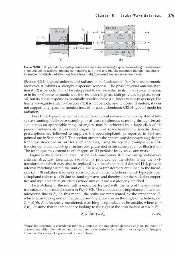
374 F r o n t i e r s i n a n t e n n a s : N e x t G e n e r a t i o n D e s i g n & e n g i n e e r i n g C h a p t e r 9 : L e a k y - W a v e a n t e n n a s 375
(Section 9.3.1) is quasi-uniform and radiates in its fundamental (n = 0) space harmonic. Moreover, it exhibits a strongly dispersive response. The phase-reversal antenna (Sec-tion 9.3.2) is periodic; it may be interpreted to radiate either in its n = -1 space harmonic or in its n = 0 space harmonic, due the ±p unit-cell phase shift provided by phase rever-sal, but its phase res ponse is essentially nondispersive (i.e., linear versus frequency). The ferrite waveguide antenna (Section 9.3.3) is nonperiodic and uniform. Therefore, it does not support any space harmonics; instead, it uses a dominant CRLH type of mode for radiation.
These three types of antennas are not the only leaky-wave antennas capable of full-space scanning. Full-space scanning, or at least continuous scanning through broad-side across an appreciable range of angles, may be achieved by a large class of 1D periodic antenna structures operating in the n = -1 space harmonic if specific design prescriptions are followed to suppress the open stopband, as reported in [44] and pointed out in Section 9.2.5. This section presents the general impedance matching design technique described in [44] for such antennas, using the specific example of a l/4-transformer stub microstrip structure also presented in this same paper for illustration. The technique may extend to other types of 1D periodic leaky-wave antennas.
Figure 9-30a shows the layout of the l/4-transformer stub microstrip leaky-wave antenna structure. Essentially, radiation is provided by the stubs, while the l/4-transformers, which may also be replaced by a matching stub if desired [44], provide internal matching within the unit cell. These l/4-transformers are tuned to the broad-side (b-1 = 0) radiation frequency, so as to prevent microreflections, which typically open a stopband (where a → 0) due to standing waves and thereby alter the radiation proper-ties and input match in structures whose unit cells are not properly matched.
The matching of the unit cell is easily performed with the help of the equivalent transmission line model shown in Fig. 9-30b. The characteristic impedance of the main microstrip line is Z0 . In this model, the stubs are represented by the impedance Zs, which naturally depend on frequency and therefore also on the angle of radiation, i.e., Zs = Zs(q). As previously mentioned, matching is optimized at broadside, where Zs = Zs(0). Assume that the impedance looking to the right of the stub located at z = 0 is16
Z Z Z1 00= = .+uru
( ) (9-49)
Figure 9-30 1D periodic microstrip leaky-wave antenna including a quarter-wavelength transformer in its unit cell to achieve impedance matching at b-1
= 0 and thereby suppress the open stopband to enable broadside radiation. (a) Trace layout. (b) Equivalent transmission line model.
Unit cell
p
w wt d2 d1 s
ws
λ/4-transformer
(a)
Unit cell
−p − (d1 + d2) − d1 0
Zs Zs
d2 d1
Z0tZ0 Z0
zZ1Z2Z3Z4Z5 = Z1
λ/4-tr.
(b)
16Since the structure is considered infinitely periodic, the impedance depends only on the point of observation within the unit cell and is invariant under periodic translation z z mp→ + (m an integer). Therefore, the choice of a given unit cell is arbitrary.
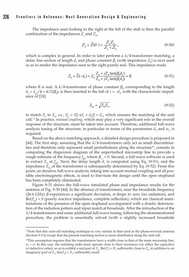
376 F r o n t i e r s i n a n t e n n a s : N e x t G e n e r a t i o n D e s i g n & e n g i n e e r i n g C h a p t e r 9 : L e a k y - W a v e a n t e n n a s 377
The impedance seen looking to the right at the left of the stub is then the parallel combination of the impedances Zs and Z0,
Z ZZ Z
Z Zs
s2
0
0
0= =+
-uru
( ) , (9-50)
which is complex in general. In order to later perform a l/4-transformer matching, a delay line section of length d1 and phase constant b1 (with impedance Z0) is next used so as to render the impedance seen to the right purely real. This impedance reads
Z Z d ZZ jZ dZ jZ d3 1 0
2 0 1 1
0 2 1 1
= - =++
ur( )
tan( )tan(
bb ))
= R (9-51)
where R is real. A l/4-transformer of phase constant b2, corresponding to the length d2 = lg2/4 = p/(2b2), is then inserted to the left of z = -d1, with the characteristic imped-ance of [24]
Z Z Zt0 0 3= , (9-52)
to match Z3 to Z0, i.e., Z4 = Z[-(d1 + d2)] = Z0, which ensures the matching of the unit cell.17 In practice, mutual coupling, which may play a very significant role in the overall response of the structure, must be taken into account. Therefore, additional full-wave analysis tuning of the structure, in particular in terms of the parameters d1 and wt, is required.
Based on the above matching approach, a detailed design procedure is proposed in [44]. The first step, assuming that the l/4-transformers only act as small discontinui-ties and therefore only represent small perturbations along the structure18, consists in computing the dispersion diagram of the unperturbed microstrip line to provide a rough estimate of the frequency fb 0 where b-1 = 0. Second, a full-wave software is used to extract Z2 at fb 0. Next, the delay length d1 is computed using Eq. (9-51), and the impedance Z0t of the transformer is subsequently determined by Eq. (9-52). From this point, an iterative full-wave analysis, taking into account mutual coupling and all pos-sible electromagnetic effects, is used to fine-tune the design until the open stopband has been completely eliminated.
Figure 9-31 shows the full-wave simulated phase and impedance results for the antenna of Fig. 9-30 [44]. In the absence of transformers, near the broadside frequency (26.6 GHz) b experiences a significant deviation, a drops to zero (no radiation), and Re(ZB) = 0 (purely reactive impedance, complete reflection), which are classical mani-festations of the presence of the open stopband accompanied with a drastic deteriora-tion of the radiation pattern and input match at broadside. After the introduction of the l/4-transformers and some additional full-wave tuning, following the aforementioned procedure, the problem is essentially solved (with a slightly increased broadside
17Note that this unit-cell matching technique is very similar to that used in the phase-reversal antenna (Section 9.3.2) except that the present matching section is more distributed along the unit cell. 18This assumption requires that the transformers have a width close to that of the main microstrip line, wt ≈ w. In this case, the radiating stubs must operate close to their resonance (on either the capacitive or inductive sides), so as to exhibit a real part of Z3, Re(Z3) = R, sufficiently close to Z0, in addition to an imaginary part of Z3, Im(Z3) = X3, sufficiently small.
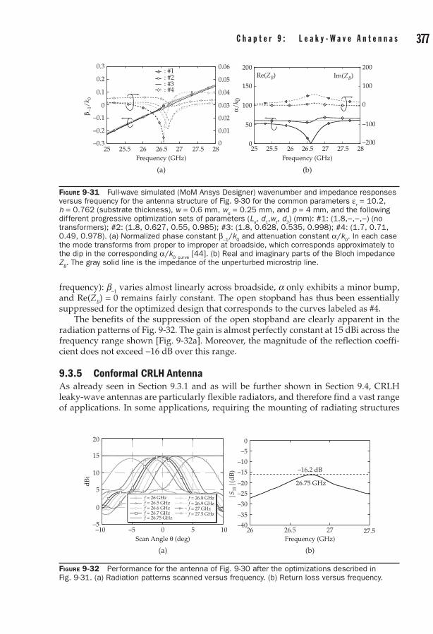
376 F r o n t i e r s i n a n t e n n a s : N e x t G e n e r a t i o n D e s i g n & e n g i n e e r i n g C h a p t e r 9 : L e a k y - W a v e a n t e n n a s 377
frequency): b-1 varies almost linearly across broadside, a only exhibits a minor bump, and Re(ZB) = 0 remains fairly constant. The open stopband has thus been essentially suppressed for the optimized design that corresponds to the curves labeled as #4.
The benefits of the suppression of the open stopband are clearly apparent in the radiation patterns of Fig. 9-32. The gain is almost perfectly constant at 15 dBi across the frequency range shown [Fig. 9-32a]. Moreover, the magnitude of the reflection coeffi-cient does not exceed -16 dB over this range.
9.3.5 Conformal CRLH AntennaAs already seen in Section 9.3.1 and as will be further shown in Section 9.4, CRLH leaky-wave antennas are particularly flexible radiators, and therefore find a vast range of applications. In some applications, requiring the mounting of radiating structures
Figure 9-31 Full-wave simulated (MoM Ansys Designer) wavenumber and impedance responses versus frequency for the antenna structure of Fig. 9-30 for the common parameters e
r = 10.2,
h = 0.762 (substrate thickness), w = 0.6 mm, ws = 0.25 mm, and p = 4 mm, and the following
different progressive optimization sets of parameters (Ls, d
1,w
t, d
2) (mm): #1: (1.8,−,−,−) (no
transformers); #2: (1.8, 0.627, 0.55, 0.985); #3: (1.8, 0.628, 0.535, 0.998); #4: (1.7, 0.71, 0.49, 0.978). (a) Normalized phase constant b-1
/k0 and attenuation constant a/k
0. In each case
the mode transforms from proper to improper at broadside, which corresponds approximately to the dip in the corresponding a/k
0 curve
[44]. (b) Real and imaginary parts of the Bloch impedance Z
B. The gray solid line is the impedance of the unperturbed microstrip line.
: #1: #2: #3: #4
β −1/
k 0
α/k 0
Frequency (GHz)
(a)
Frequency (GHz)
Re(ZB) Im(ZB)
(b)
0.3
0.2
0.1
0
–0.1
–0.2
–0.325 25.5 26 26.5 27 27.5 28
0
0.01
0.02
0.03
0.04
0.05
0.06 200
150
100
50
025 25.5 26 26.5 27 27.5 28
–200
–100
0
100
200
Figure 9-32 Performance for the antenna of Fig. 9-30 after the optimizations described in Fig. 9-31. (a) Radiation patterns scanned versus frequency. (b) Return loss versus frequency.
Scan Angle θ (deg)
dB
i
(a)
Frequency (GHz)
|S 1
1|(d
B)
(b)
20
15
10
5
0
–5–10 –5
f = 26 GHzf = 26.5 GHzf = 26.6 GHzf = 26.7 GHzf = 26.75 GHz
f = 27.5 GHzf = 27 GHzf = 26.9 GHzf = 26.8 GHz
0 5 10 26 26.5 27 27.5
–16.2 dB
26.75 GHz
–40
–35
–30
–25
–20
–15
–10
–5
0

378 F r o n t i e r s i n a n t e n n a s : N e x t G e n e r a t i o n D e s i g n & e n g i n e e r i n g C h a p t e r 9 : L e a k y - W a v e a n t e n n a s 379
on curved surfaces, such as for instance the conical nose of a plane or a cylindrical mast, the antenna must be conformal, i.e., capable to adapt to the geometry of the sur-face while maintaining desired characteristics. This section presents a technique to realize conformal CRLH leaky-wave antennas.
Conformal CRLH leaky-wave antennas were first reported in [45], [46]. Their prin-ciple of operation is depicted in Fig. 9-33 for a shape consisting of three adjacent sides of a dodecagonal cylinder, requiring three different leaky-wave antenna sections. Each CRLH section is uniform and is designed to radiate at the proper angle with respect to its surface so that it contributes to the overall antenna radiation pattern at the desired angle and thereby permits maximal directivity. If the antenna is to radiate at a unique angle (e.g., broadside, middle case in Fig. 9-33), the design is relatively easy. In con-trast, providing scanning requires a more involved dispersion engineering design proce-dure, where the group velocities of all the sections, vg = ∂ /∂w b , must be sufficiently small to set all the frequencies of interest within visible space, and yet not too small to avoid an excessive phase sensitivity ∂ /∂b w , which would compromise the bandwidth of the antenna. The concept can be straightforwardly extended to other shapes, and piece-wise uniform antenna sections may be used to match shapes with a continuous curvature.
Figure 9-34 shows a three-section CRLH conformal leaky-wave antenna prototype, where the three sections approximate a continuous-curvature circular cylindrical shape. In order to avoid reflections, all the CRLH radiating sections must exhibit the same Bloch impedance, which requires the simultaneous adjustment of the interdigital capacitors and stub inductors (Eq. (43b)). The transitions and sections structures on each side are shown in the insets of the figure.
Figure 9-35 shows three sets of experimental radiation patterns at three frequencies (backward, broadside, and forward) for the following cases: (i) flat (nonconformal) fully uniform (only one section overall) antenna, (ii) fully-uniform antenna but bent so as to conform to the cylinder’s shape, (iii) conformal antenna shown in Fig. 9-34 with three different sections. The following observation may be made. The three types of structures scan the beam toward the expected direction. The flat uniform structure
Figure 9-33 Principle of conformal CRLH leaky-wave antennas, shown here for the case of a shape consisting of three adjacent sides of a dodecagonal cylinder, requiring three different uniform leaky-wave antenna sections, labeled 1, 2, and 3, with a 150° internal angle. The top sketches show the shape of the antenna and the radiation angles of its three sections. The bottom graphs show the dispersion relations of the three sections and indicate the points of operation of the three structures for the three corresponding radiation regimes at three representative frequencies (BWD: backward, BS: broadside, and FWD: forward).
12
3
FWD BWDBS
12
3
FWD+FWD
BS
12
3
BWD+BWD
BS
1
23
1
23
1
23
β ββ
ωωf = fBWD f = fBS f = fFWD
ω
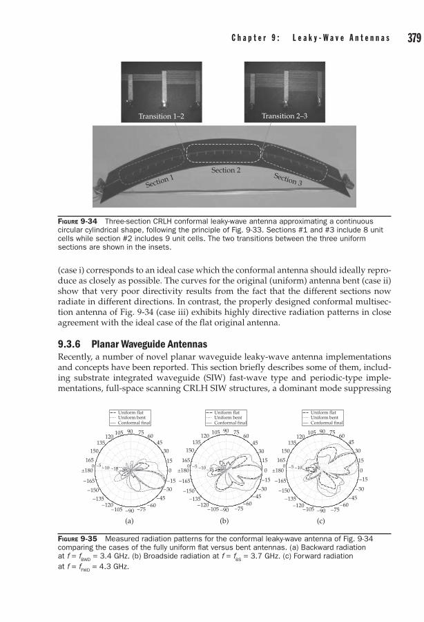
378 F r o n t i e r s i n a n t e n n a s : N e x t G e n e r a t i o n D e s i g n & e n g i n e e r i n g C h a p t e r 9 : L e a k y - W a v e a n t e n n a s 379
(case i) corresponds to an ideal case which the conformal antenna should ideally repro-duce as closely as possible. The curves for the original (uniform) antenna bent (case ii) show that very poor directivity results from the fact that the different sections now radiate in different directions. In contrast, the properly designed conformal multisec-tion antenna of Fig. 9-34 (case iii) exhibits highly directive radiation patterns in close agreement with the ideal case of the flat original antenna.
9.3.6 Planar Waveguide AntennasRecently, a number of novel planar waveguide leaky-wave antenna implementations and concepts have been reported. This section briefly describes some of them, includ-ing substrate integrated waveguide (SIW) fast-wave type and periodic-type imple-mentations, full-space scanning CRLH SIW structures, a dominant mode suppressing
Figure 9-34 Three-section CRLH conformal leaky-wave antenna approximating a continuous circular cylindrical shape, following the principle of Fig. 9-33. Sections #1 and #3 include 8 unit cells while section #2 includes 9 unit cells. The two transitions between the three uniform sections are shown in the insets.
Transition 1–2 Transition 2–3
Section 1Section 2
Section 3
Figure 9-35 Measured radiation patterns for the conformal leaky-wave antenna of Fig. 9-34 comparing the cases of the fully uniform flat versus bent antennas. (a) Backward radiation at f = f
BWD = 3.4 GHz. (b) Broadside radiation at f = f
BS = 3.7 GHz. (c) Forward radiation
at f = fFWD
= 4.3 GHz.
−75
0
15
30
4560
7590105120
135150
165
±180
−165
−150
−135−120
−105 −90−60
−45
−30
−15
−20−15−10−50
(a)
−75
0
15
30
4560
7590105120
135150
165
±180
−165
−150−135
−120−105 −90
−60−45
−30
−15
−20−15−10−50
Uniform bentConformal final
Uniform flatUniform bentConformal final
Uniform flat
(b)
−75
0
15
30
4560
7590105120
135150
165
±180
−165
−150−135
−120−105 −90
−60−45
−30
−15
−20−15−10−50
(c)
Uniform bentConformal final
Uniform flat

380 F r o n t i e r s i n a n t e n n a s : N e x t G e n e r a t i o n D e s i g n & e n g i n e e r i n g C h a p t e r 9 : L e a k y - W a v e a n t e n n a s 381
half-width EH1 microstrip structure, an enhanced-bandwidth inhomogeneous EH1 microstrip structure, and nonradiating dielectric strip waveguide structures with sepa-rately controllable phase and leakage constants.
An SIW is low-profile planar rectangular waveguide which is directly integrated on a substrate by using arrays of closely-spaced plated vias (period much smaller than lg) as equivalent lateral walls19 and simple strip metallizations on both sides of the substrate for the top and bottom walls20 [47]. Figure 9-36 shows two implementations of conventional leaky-wave antennas in SIW technology. In both cases, the substrate is cut off along the edge of one of the two lateral walls to allow radiation at the resulting dielectric-air interface, where the direction of radiation is modified by Snell’s law. The first antenna, shown in Fig. 9-36a, is a fast-wave type waveguide structure, which must satisfy the condition k a r0 > /p e( ) to maintain the phase constant b e p= - /rk a0
2 2( ) of the weakly-perturbed TE10 dominant mode real [48]. The radiation range is further restricted by the critical angle of Snell’s law. The leakage constant of the structure becomes significant when the distance between the vias exceeds twice their diameter and can be modulated by controlling the lengths and number of lateral apertures. The structure can be conveniently analyzed by the transverse resonance technique, model-ing the vias by an equivalent conductance, given in [49] for the case of an infinite array of metallic cylinders. The second antenna, shown in Fig. 9-36b, is a periodic type waveguide structure radiating in the n = -1 space harmonic [50]. This antenna is also capable of operating in the TE20 mode (prototype shown in Fig. 9-36b) with radiation from both edges and improved radiation properties.
Another form of SIW leaky-wave antenna consists of an SIW waveguide with transverse slots in the top wall of the SIW, as shown in Fig. 9-37 [51]. The structure
19Such a waveguide is essentially equivalent to a waveguide with continuous walls for the dominant TE10 mode, which is the mode generally used. Due to the open circuits between the vias in the direction of propagation, modes with a nonzero longitudinal component of the surface current, such as the higher order modes TM11 and TE11, are not allowed. 20Therefore, the height of the waveguide is the height of the substrate.
Figure 9-36 Substrate integrated waveguide (SIW) implementation of conventional leaky-wave antennas. (a) Fast-wave type structure [48]. (b) Periodic-type structure operating in the n = -1 space harmonic [50]. A TE
20-mode prototype (also possible in addition to the TE
10-mode
structures) excited by a double microstrip line following a divider is also shown, where elongated plated vias are used instead of circular posts.
a
s
c d1
d2
yz
xInputpoint
Leaky-w
ave
(a) (b)
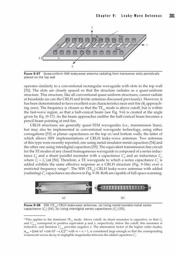
380 F r o n t i e r s i n a n t e n n a s : N e x t G e n e r a t i o n D e s i g n & e n g i n e e r i n g C h a p t e r 9 : L e a k y - W a v e a n t e n n a s 381
operates similarly to a conventional rectangular waveguide with slots in the top wall [52]. The slots are closely spaced so that the structure radiates as a quasi-uniform structure. This structure, like all conventional quasi-uniform structures, cannot radiate at broadside (as can the CRLH and ferrite antennas discussed previously). However, it has been demonstrated to have excellent scan characteristics near end-fire (q0 approach-ing zero). The frequency is chosen so that the TE10 mode is above cutoff, but is within the fast-wave region, so that a half-conical beam (see Fig. 9-6) is created at the angle given by Eq. (9-17). As the beam approaches endfire the half-conical beam becomes a pencil beam pointing at end-fire.
CRLH structures are generally quasi-TEM waveguides (i.e., transmission lines), but may also be implemented in conventional waveguide technology, using either corrugations [53] or planar capacitances on the top or/and bottom walls, the latter of which allows SIW implementations of CRLH leaky-wave antennas. Two antennas of this type were recently reported, one using metal-insulator-metal capacitors [54] and the other one using interdigital capacitors [55]. The equivalent transmission line circuit for the TE modes of any closed homogeneous waveguide is composed of a series induc-tance L’R and a shunt parallel resonator with a capacitance C’R and an inductance L’L, where L’L = L’L (w) [56]. Therefore, a TE waveguide to which a series capacitance C’L is added exhibits the same effective response as a CRLH structure (Fig. 9-18a) over a restricted frequency range21. The SIW (TE10) CRLH leaky-wave antennas with added (radiating) C’L capacitance are shown in Fig. 9-38. Both are capable of full-space scanning.
Figure 9-37 Quasi-uniform SIW leaky-wave antenna radiating from transverse slots periodically placed on the top wall
Via
Slot
εr
s θ0
p
x
y
zw
h
21This applies to the dominant TE10 mode. Above cutoff, its shunt resonator is capacitive, so that L’R and C’R,eq correspond to positive equivalent m and e, respectively; below the cutoff, this resonator is inductive, and therefore L’L,eq provides negative e. The attenuation factor of the higher order modes, a p p emn = / + / - /[( ) ( ) ]m a n b kr
2 202 1 2 with m + n > 1, is considered large enough so that the corresponding
evanescent waves decay to negligible magnitudes between the added capacitors C’L.
Figure 9-38 SIW (TE10
) CRLH leaky-wave antennas. (a) Using metal-insulator-metal series capacitance (C
L) [54]. (b) Using interdigital series capacitance (C
L) [55].
(a) (b)
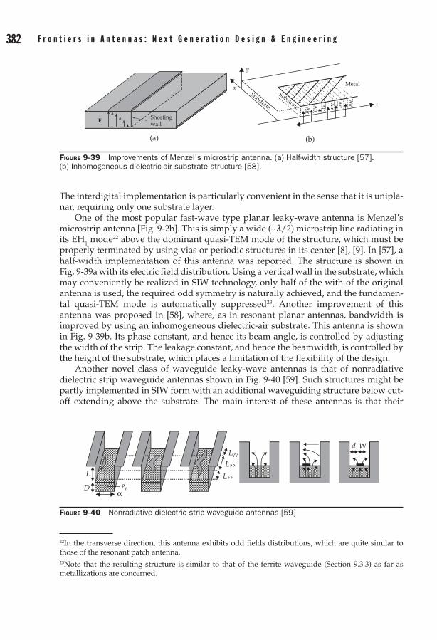
382 F r o n t i e r s i n a n t e n n a s : N e x t G e n e r a t i o n D e s i g n & e n g i n e e r i n g C h a p t e r 9 : L e a k y - W a v e a n t e n n a s 383
The interdigital implementation is particularly convenient in the sense that it is unipla-nar, requiring only one substrate layer.
One of the most popular fast-wave type planar leaky-wave antenna is Menzel’s microstrip antenna [Fig. 9-2b]. This is simply a wide (∼l/2) microstrip line radiating in its EH1 mode22 above the dominant quasi-TEM mode of the structure, which must be properly terminated by using vias or periodic structures in its center [8], [9]. In [57], a half-width implementation of this antenna was reported. The structure is shown in Fig. 9-39a with its electric field distribution. Using a vertical wall in the substrate, which may conveniently be realized in SIW technology, only half of the with of the original antenna is used, the required odd symmetry is naturally achieved, and the fundamen-tal quasi-TEM mode is automatically suppressed23. Another improvement of this antenna was proposed in [58], where, as in resonant planar antennas, bandwidth is improved by using an inhomogeneous dielectric-air substrate. This antenna is shown in Fig. 9-39b. Its phase constant, and hence its beam angle, is controlled by adjusting the width of the strip. The leakage constant, and hence the beamwidth, is controlled by the height of the substrate, which places a limitation of the flexibility of the design.
Another novel class of waveguide leaky-wave antennas is that of nonradiative dielectric strip waveguide antennas shown in Fig. 9-40 [59]. Such structures might be partly implemented in SIW form with an additional waveguiding structure below cut-off extending above the substrate. The main interest of these antennas is that their
Figure 9-39 Improvements of Menzel’s microstrip antenna. (a) Half-width structure [57]. (b) Inhomogeneous dielectric-air substrate structure [58].
E Shortingwall
(a) (b)
y
x
z
Metal
Substrate
Substrate Air
Air
Air
Air
Air
Air
Figure 9-40 Nonradiative dielectric strip waveguide antennas [59]
L
L??
L??
L??
Dα
εr
d W
22In the transverse direction, this antenna exhibits odd fields distributions, which are quite similar to those of the resonant patch antenna.23Note that the resulting structure is similar to that of the ferrite waveguide (Section 9.3.3) as far as metallizations are concerned.

382 F r o n t i e r s i n a n t e n n a s : N e x t G e n e r a t i o n D e s i g n & e n g i n e e r i n g C h a p t e r 9 : L e a k y - W a v e a n t e n n a s 383
phase constant b and leakage constant a can be controlled almost independently. The former is determined by the position and shape of the strip on top of the substrate, while the latter is determined by the transverse size of the waveguide, which may be easily tapered for sidelobe level control.
9.3.7 Highly-Directive Wire-Medium AntennaThe recent interest in artificial materials (metamaterials) has led to an interesting new type of radiating structure, in which a source is placed inside of an artificial material consisting of a wire medium (or something equivalent to a wire medium). Such struc-ture were actually first introduced quite some time ago [60], [61], though much recent attention has been devoted to them [62]–[65]. The structure shown in Fig. 9-41 consists of a “slab” of artificial medium over a ground plane, where the artificial medium is composed of a periodic arrangement of closely-spaced metallic wires or rods. The wires (assumed to be perfectly conducting here) have a radius a and are spaced peri-odically with periods px and pz in the x and z directions, respectively, and are infinite in the y direction. A finite number N of wire rows are stacked vertically in the z direction to form the artificial slab (the figure shows N = 4, though in practice many more rows would be used). The bottom row is elevated pz/2 above the ground plane. Although it is not completely obvious how to best define the height h of the artificial slab, a natural choice is h = Nd, and this choice will be adopted here. That is, the slab boundary at z = 0 is defined at a distance pz /2 above the top row of wires. Two sources have been stud-ied: an infinite electric line source in the y direction [66] and a y-directed infinitesimal electric dipole [67]. In either case the source is assumed to be located at x = 0 and z = -hs, where hs is the embedding distance to the top interface.
If the wire radius a is very small compared to the periodicities, and the periods are also much smaller than the wavelength inside the wire medium, the wire medium can be homogenized, i.e., described as an artificial homogeneous medium with an aniso-tropic permittivity that is approximately described by the dyadic permittivity [68]
e e= --
+ +
0
2
02 21k
k kp
y
ˆ ˆ ˆ ˆ ˆ ˆyy xx zz. (9-53)
Figure 9-41 Side view of an artificial wire-medium slab excited by either an infinite electric line source or a y-directed horizontal electric dipole source
xy
z
px
pzh Wires
Ground plane
Sourcehs
384 F r o n t i e r s i n a n t e n n a s : N e x t G e n e r a t i o n D e s i g n & e n g i n e e r i n g C h a p t e r 9 : L e a k y - W a v e a n t e n n a s 385
Note that the metallic wires only affect the yy component of the permittivity, under the assumption that the wires radius is very small. An approximate expression for the “plasma wavenumber” kp that appears in the above equation is [69]
kF
Fpp p
p pa
n
x z
x z
=
+
, = - +2
22
p
p uu u
ln ( )( )
ln( )
==
∞
∑ - + ,1
16
coth( )p u punn
(9-54)
where u = px/pz. The permittivity result in Eq. (9-53) assumes that the medium is excited by a plane wave, which is associated with wavenumbers kx , ky, and kz. Note that that the yy component of the permittivity dyad eyy depends on frequency, and hence the medium is said to exhibit temporal dispersion. The component eyy also depends on the wavenumber ky , and because of this the medium is also said to exhibit spatial dispersion.
For the case of plane-wave incidence normal to the wire axis, for which ky = 0, the permittivity expression simplifies to
e eww
= -
+ +
0
2
21 p ˆ ˆ ˆ ˆ ˆ ˆyy xx zz (9-55)
where wp is a constant defined by kp p2 2
0 0= w m e that is termed the “plasma frequency” of the wire medium, since the frequency response of eyy in eq. (9-55) is exactly that of a lossless plasma having a plasma resonance frequency wp [70]. Note that for a line-source excitation there will be no y variation in the problem, and hence Eq. (9-55) may be used, while for a dipole excitation Eq. (9-53) should be used. The field of the y-directed dipole source may be constructed, via superposition (as a Fourier integral), as a spectrum of fields from infinite phased line sources, with currents varying as exp(-jkyy). Each spectral component will see a different permittivity eyy(w).
Eq. (9-55) shows that the yy component of the relative permittivity, er,yy, is positive for frequencies above the plasma frequency, and negative for frequencies below it. Hence, a homogenized artificial wire medium can have an effective relative permittiv-ity that is either negative or positive but less than unity. For frequencies that are above, but close to, the plasma frequency, the relative permittivity er,yy will be positive but very small. This is the frequency region for which highly directive beams may be created. To illustrate this, consider first the simpler case of the infinite line source excitation, for which Eq. (9-55) applies. The homogenized model is shown in Fig. 9-42a. In Fig. 9-42b the case is shown where the slab thickness is infinite, corresponding to a half-space of low-permittivity material. Because there is no y variation, an isotropic material may be assumed with er = er,yy. A narrow beam at broadside is created when operating close to but slightly above the plasma frequency, i.e., 0 < er,yy << 1, as illustrated in Fig. 9-42. A simple explanation of the narrow beam effect may be provided by a ray picture, in which rays emanating from the source refract at the slab interface according to Snell’s law, and are bent toward the normal [71]. The lower the relative permittivity of the slab, the more directive is the beam, since the angles of the rays as they exit the slab are closer to the normal direction (the z-axis).
For the case where the slab thickness is very large so that it may effectively be replaced by a semi-infinite half-space of material, the ray-optic analysis yields a com-plete explanation for the narrow-beam effect. (Technically speaking, in order for the

384 F r o n t i e r s i n a n t e n n a s : N e x t G e n e r a t i o n D e s i g n & e n g i n e e r i n g C h a p t e r 9 : L e a k y - W a v e a n t e n n a s 385
slab to approximate a half-space as the slab thickness increases, a small amount of loss in the slab must be assumed [71].) The far-field pattern for the field component Ey that is radiated by the line source located at (x, z) = (0, −hs) may be conveniently calcu-lated by using reciprocity [17]. In this calculation, a y-polarized plane wave is incident on the structure at an angle q from the z-axis, and the field Ey(0, z) is calculated at the location (0, -hs). Under plane-wave incidence, the field Ey(0, z) inside the homogenized slab may be determined by means of a simple transverse equivalent network for the structure, and hence the exact far-field pattern is easily determined [17]. Results show that the far-field pattern is fairly constant near broadside over an angular region −qc < q < qc, where qc is the critical angle given by sinq ec r= ,yy . (The angle q here is allowed
to be positive or negative, as indicated in Fig. 9-42.) Outside this angular region the pattern decays rapidly, with the rate of decay increasing as the distance hs increases. Physically, this behavior is expected due to the nature of the critical angle, with the field Ey inside the slab decaying exponentially with vertical distance away from the interface when the structure is illuminated by an incident plane wave arriving from an angle |q| > qc. By reciprocity, the far-field pattern is thus also small for angles in this range. Hence, for sources that are embedded far enough away from the interface, the beamwidth is approximately given by ∆q = 2qc, and the beamwidth is thus directly proportional to er ,yy . The beam is illustrated in Fig. 9-42b. If one plots the field Ey(x, 0) along the interface due to the line source, one observes a field that decays with distance as |x|−3/2, expected from an asymptotic analysis of an interface problem [71].
It has been found that significantly narrower beams than that obtained in the half-space problem may be produced when the slab has a finite thickness, as shown in Fig. 9-42a, if the thickness is properly optimized. An optimum thickness that maxi-mizes the power density radiated at broadside (and approximately minimizes the beamwidth) occurs when
h hn n
n …r
= = = = , , ,opt,
l le
e2 2
1 2 30
yy
(9-56)
where le is the wavelength inside the slab. The thinnest slab satisfying Eq. (9-56) corre-sponds to one that is a half-wavelength thick in the artificial material. The physical slab
Figure 9-42 Illustration of the beams produced by a line source inside of an artificial material with a low permittivity. (a) A finite-thickness slab produces a narrow beam at broadside when the slab thickness is optimized. (b) A semi-infinite half space produces a beam that is nearly constant within an angular region defined by the critical angle.
x
z
hεr = εr, yy hs
Line source
θ
(a)
x
z
hs
Line sourceinfinite half space
(b)
εr = εr, yy

386 F r o n t i e r s i n a n t e n n a s : N e x t G e n e r a t i o n D e s i g n & e n g i n e e r i n g C h a p t e r 9 : L e a k y - W a v e a n t e n n a s 387
thickness increases as the permittivity decreases. Although the ray-optic effect is still present for the slab problem, it is found that a leaky wave is responsible for the narrow-beam effect in the optimized slab problem. A bidirectional leaky wave is launched by the source (see Section 9.2.3), producing a narrow beam at broadside as shown in Fig. 9-42a [66]. An analysis reveals that when the optimum slab thickness from Eq. (9-56) is used, the leaky wave has a wavenumber kz = b - ja given by b/k0 ≈ a/k0 ≈ e pr n,yy
3 4 1 2/ //( ) . From Section 9.2.3, a leaky wave having b ≈ a will produce a pattern having a beam-width ∆ = /q a2 2 0( )k [see Eq. (9-28)]. Hence, the beamwidth in the optimum slab case
is proportional to er ,yy3 4/ instead of er ,yy
1 2/ as it is in the half-space case. Hence, for low per-mittivities, much narrower beams may be produced in the slab case than the half-space case, for the same permittivity. The power radiated by the line source is maximized when the source is located in the middle of the slab [66], although the source position does not significantly affect the beam shape (which is determined by the wavenumber of the leaky wave). Although narrow beams may be created with the wire-medium slab structure, an obvious disadvantage is that the physical slab thickness is large for low permittivities and low frequencies (from Eq. (9-56)). This limitation may not be too severe at high frequencies, but at lower frequencies it presents a serious restriction.
It is interesting to compare the performance of the wire-medium slab leaky-wave antenna with that of a more conventional parallel-plate leaky wave antenna consisting of a partially reflecting surface (PRS) at a height h over a ground plane [17]. The PRS may be constructed in various ways, e.g, by using a high-permittivity dielectric layer or by using a grid of metallic wires or strips (see Fig. 9-43 in Section 9.3.8). For this structure the power radiated at broadside is also approximately maximized when Eq. (9-56) is satisfied, with er,yy now referring to the relative permittivity of the actual material inside the parallel-plate region. The directivity increases as the normalized shunt susceptance s sB B= η0 of the PRS in the transverse equivalent network model increases (see Fig. 9-8). For either type of antenna, the beam may be made arbitrarily narrow by either lowering the effective permittivity (wire-medium case) or increasing the value of sB (PRS case). For the same beamwidth, a figure of merit that may be used to compare the two antennas is the fractional pattern bandwidth BW, defined by the lower and upper frequency limits f1 and f2 where the power density at broadside has dropped by 3 dB from that at the design frequency f0, that is, BW = (f2 - f1)/f0. An analy-sis reveals that the wire-medium slab antenna has a bandwidth of BW = 2(a/k0)
2 [66] while the PRS antenna has a bandwidth of BW = 2(a/k0)
2/(er mr) [17], where er and mr are the parameters of the parallel-plate region. Hence, for a PRS structure having an air-filled parallel-plate region, the two structures will have the same bandwidth. The PRS struc-ture will be much thinner in height, however. As an interesting side note, if the wire medium is replaced by a hypothetical dispersionless low-permittivity material with a fre-quency-independent value of er,yy, the bandwidth will increase to BW = (2/p 2/3)(a/k0)
2/3. However, such a medium is not practically attainable, at least with simple wires [72].
The results discussed above for the line source may be extended to the case of the y-directed dipole excitation. The H-plane (xz-plane) pattern of the line source and the horizontal electric dipole are the same, so the results discussed for the line source are applicable for the H-plane of the dipole as well. When the optimum slab thickness is used from Eq. (9-56), the beam produced by the dipole is a narrow azimuthally sym-metric pencil beam at broadside, with nearly equal E- and H-plane beamwidths, as shown in Fig. 9-17b. When the slab thickness is increased from the optimum value the leaky wave will have b > a and a conical beam will form as shown in Fig. 9-17a, typical of radiation from a radially-propagating 2D leaky-wave.
386 F r o n t i e r s i n a n t e n n a s : N e x t G e n e r a t i o n D e s i g n & e n g i n e e r i n g C h a p t e r 9 : L e a k y - W a v e a n t e n n a s 387
One interesting feature of the conical beam that is produced by the dipole when b > a is that the beam angle q0 is azimuthally symmetric (independent of j), as opposed to the more conventional PRS-based parallel-plate 2D leaky-wave antenna, where the beam angle is only approximately independent of j, and exhibits more variation with azimuth angle j [73]. This interesting property of the wire-medium structure arises from the fact that a radially-propagating TMx leaky wave is responsible for the pattern, and this leaky wave has a radial wavenumber kr = b - ja that is independent of the angle j of propagation on the structure. This propagation property in turn arises by virtue of the fact that the wire medium has spatial dispersion, with er,yy being a function of the angle j, due to the ky term in Eq. (9-53). This might at first seem counter-intuitive, that having a relative permittivity that is angle dependent would lead to a leaky wave whose wavenumber is independent of angle. However, if one constructed a leaky-wave antenna by using an isotropic low-permittivity slab instead of an anisotropic wire-medium slab, the leaky-wave propagation from the dipole source would not be isotropic. This is because two leaky waves would be excited by the horizontal electric dipole, a TMz wave and a TEz wave, as discussed in Section 9.2.6. The TMz leaky wave would have a sin j dependence and would primarily determine the shape of the E-plane pattern, while the TEz leaky wave would have a cosj dependence and would primarily determine the H-plane pattern (see Eq. (9-39)). These two leaky waves would have slightly different wavenumbers, so the overall leaky-wave propagation, accounting for both waves, would be angle dependent. In a sense, the anisotropic nature of the wire medium compensates for the natural anisotropic nature of the leaky-wave propagation that an isotropic slab would have, resulting in a single TMx leaky wave that propagates isotropically. This single TMx leaky wave is equivalent to pair of TMz and TEz leaky waves that have the same wavenumber, which is independent of j. Another structure that supports isotropic leaky-wave propagation, and is thinner than the wire-medium slab structure, is the MSG PRS structure discussed below in Section 9.3.8.
9.3.8 2D Metal Strip Grating (MSG) Partially Reflective Surface (PRS) Antenna
One class of 2D leaky-wave antennas that has become very popular recently is the par-tially reflecting surface (PRS) class of structures. This type of structure was mentioned in Section 9.2.3 in connection with a 1D leaky-wave antenna, and many of the remarks made there apply also to the 2D case. A PRS structure consists of a grounded dielectric substrate on top of which is placed a PRS, forming a leaky parallel-plate waveguide region. A source such as a horizontal electric dipole will excite radially-propagating leaky waves, which are leaky versions of the TM1 and TE1 parallel-plate modes that would exist if the PRS were a perfectly conducting sheet. Examples of PRS structures are shown in Fig. 9-43, where The PRS consists of a high-permittivity dielectric layer (Fig. 9-43a) [74], a stack of dielectric layers [Fig. 9-43(b)] [75, 76], a periodic array of metal patches (Fig. 9-43c) [77], or a periodic array of slots (Fig. 9-43d) [78].
The type of source inside the parallel-plate region determines what type of leaky waves get excited in accordance with the discussion of 2D leaky-wave radiation in Section 9.2.6. A vertical dipole source will excite an azimuthally-symmetric leaky wave that is independent of j for the structures of Figs. 9-43a and 9-43b, and this will radiate a perfectly symmetric beam at some scan angle q = q0 as discussed in Section 9.2.6. Fig. 9-17a shows an example of such a beam. The polarization of the far-field pattern will depend on the type of source (electric or magnetic dipole) An azimuthally-symmetric beam cannot be produced by a vertical dipole source inside the structures of Figs. 9-43c
388 F r o n t i e r s i n a n t e n n a s : N e x t G e n e r a t i o n D e s i g n & e n g i n e e r i n g C h a p t e r 9 : L e a k y - W a v e a n t e n n a s 389
and 9-43d. A horizontal dipole can radiate either a pencil beam at broadside or a coni-cal beam at a scan angle q = q0 (see Fig. 9-17). Either type of beam may be created with a horizontal dipole using any of the structures shown in Fig. 9-43. The leaky-wave fields in Eq. (9-38) assume either an electric dipole in the x direction or a magnetic dipole in the y direction, and this is the assumed orientation here. For an electric dipole, maximum power is radiated when the source is placed in the middle of the parallel-plate region (z = -hs = -h/2) while a magnetic dipole radiates maximum power when placed at the ground plane (z = -hs = -h).
The far-field pattern may be calculated by reciprocity, in which the field at the dipole source location is calculated from an incident plane wave impinging on the PRS structure [77]. The plane-wave incident problem is modeled using a transverse equiva-lent network as shown in Fig. 9-8. The far-field components Eq and Ef correspond to TMz and TEz transmission line models in the equivalent circuit. Assuming an homogenized PRS [79] as in Fig. 9-8, the far field in the E-plane (j = 0) contains only Eq and in the H-plane (j = p/2) only Ej.
For a broadside beam, maximum power density is radiated at broadside when the substrate thickness is approximately one-half of a wavelength in the substrate dielectric. For the case of a lossless metallic PRS, such as the periodic array of metal patches or slots, the PRS is modeled as a lossless shunt susceptance as shown in Fig. 9-8. In this case there is a slight de-tuning away from the half-wavelength thickness, and maxi-mum power density is radiated when the substrate thickness is chosen as [80]
cot( )k h Br
rs1 = ,
me
(9-57)
where k1 is the wavenumber of the substrate, s sB B= η0 is the normalized shunt suscep-tance modeling the PRS in Fig. 9-8, and the parameters mr and er pertain to the substrate.
Figure 9-43 Examples of PRS structures that have a partially reflecting surface (PRS) over a grounded substrate, forming a leaky parallel-plate region. An x-directed horizontal electric dipole source inside the substrate is shown as the source. The PRS consists of: (a) a high permittivity dielectric layer, (b) a stack of dielectric layers, (c) a periodic array of metal patches, and (d) a periodic array of slots in a conducting plate.
x
yz
h
(a)
x
yz
h
(b)
x
yz
h
(c)
x
yz
h
(d)

388 F r o n t i e r s i n a n t e n n a s : N e x t G e n e r a t i o n D e s i g n & e n g i n e e r i n g C h a p t e r 9 : L e a k y - W a v e a n t e n n a s 389
(For the structures shown in parts (a) and (b) of Fig. 9-43, the dielectric superstrate layers have a nonzero thickness, but the radiation performance can still be approximately modeled with an equivalent shunt susceptance [81].) When the substrate thickness is optimized according to Eq. (9-57), the two radial leaky waves that are excited by the dipole source, the TMz wave and the TEz wave, will have nearly equal wavenumbers, and for each wave b ≈ a, consistent with the discussion in Section 9.2.3 for 1D leaky waves. A pencil beam at broadside that is nearly azimuthally symmetric will be created when Eq. (9-57) is satisfied, regardless of the symmetry of the PRS. For example, the PRS may consist of a two-dimensional periodic array of narrow slots in a conducting plane [78], with the slot axes perpendicular to an electric dipole source as in Fig. 9-43d. (Slots parallel to a magnetic dipole source could also be used.) In addition to the very different length and width dimensions of the slots, the periodicities may also be completely dif-ferent in the x and y directions. Although such a PRS is clearly not azimuthally symmet-ric, and appears quite different along the x and y directions, the broadside beam will nevertheless be nearly azimuthally symmetric, as illustrated in Fig. 9-17b. This is a con-sequence of the fact that the characteristic impedance of the transmission line as well as the value of Bs in Fig. 9-8 are nearly the same in the E- and H-planes for small angles q.
Although essentially any PRS (such as the ones shown in Fig. 9-43) can be used to create a symmetric pencil beam at broadside, the situation worsens when using the PRS structure to produce a conical beam at a scan angle q0. Such a beam, shown in Fig. 9-17a, will be produced for a substrate thickness given approximately as [80]
k h r r02
0m e q p- =sin (9-58)
where mr and er describe the substrate. As the substrate thickness increases from the value given in Eq. (9-57) to the one in Eq. (9-58), the pencil beam at broadside “opens up” and becomes a conical beam pointing approximately at an angle q0 given by Eq. (9-58). However, for most PRS structures the exact beam angle q0 is a function of the azimuth angle j, for q0 > 0. This is because the two fundamental leaky waves that are excited by the source, the TMz and the TEz waves (see Eq. (9-38)), have different wave-numbers, so that k kρ ρ
TM TE≠ . The wavenumbers typically become more different as the scan angle q0 increases, so that the beam angles in the E- and H-planes become increas-ingly different as the scan angle increases. This would normally be undesirable.
It was recently discovered that one particular type of PRS does not suffer from this difficulty, and hence the beam angle is independent of azimuth angle. This is the PRS consisting of a 1D periodic array of narrow metal strips, as shown in Fig. 9-44. The metal
Figure 9-44 Metal-strip grating (MSG) leaky-wave antenna, shown with a horizontal x-directed electric dipole excitation. The MSG is at z = 0 and the dipole is located at z = -h
s.
x
yz
p
w
h Substrate

390 F r o n t i e r s i n a n t e n n a s : N e x t G e n e r a t i o n D e s i g n & e n g i n e e r i n g C h a p t e r 9 : L e a k y - W a v e a n t e n n a s 391
strips have a width w and a periodic spacing p that are both small compared with a wavelength (w < p << lg). This interesting property of omnidirectional propagation exactly holds when the substrate is air, and approximately otherwise. Hence, an air substrate will be assumed here.
Although it is certainly not obvious, such a structure will have azimuthally sym-metric leaky-wave propagation [73], and hence a beam angle that is independent of azimuth angle [82], [83]. Assuming an air substrate and narrow strips, a single TMx leaky wave will be supported by the structure, since the current on the strips is x-directed. Hence, for any angle of propagation j a single TMx leaky-wave propagates, instead of a pair of TMz and TEz leaky waves that would propagate on the structures shown in Figs. 9-43a and 9-43b. Hence, the circuit model shown in Fig. 9-8 must be modified for the MSG structure, so that the characteristic impedance of the transmis-sion line is based on a TMx wave. The characteristic admittance is [73]
YZ
k k
k kk k k kx
x
z
xz x0
0
0 0
0 02 2 0 0
2 21TMTM= =
-( ) , = - -η yy k k2
02 2= - .ρ (9-59)
An approximate expression for the sheet susceptance of a MSG that is homogenized is [49]
Bkp k k
s
xwp
= --( ) ( )
.2 10
002 2
2
pη pln csc
(9-60)
Comparing Eqs. (9-59) and (9-60), it is seen that both the characteristic admittance and the PRS sheet susceptance vary with angle of propagation j by virtue of the same term k kx0
2 2- . The transverse resonance equation becomes
k k
k kj k h jB kz
xz s x
0 0
0 02 2 01 0
η -( ) - + = .cot( ) ( ) (9-61)
Inserting Eq. (9-60) into Eq. (9-61), it is seen that because of the common factor k kx02 2- ,
the solution of Eq. (9-61) for the modal wavenumber kr = b - ja does not depend on angle j. Hence, kr is not a function of angle j when using the MSG as a PRS.
To illustrate this fact, Fig. 9-45 shows a pattern obtained from a typical MSG PRS structure that has a scan angle of about 12 degrees at a frequency of 20.5 GHz [82]. It is seen that the far-field patterns in the E-plane (j = 0) and the H-plane (j = p/2) are essen-tially identical. Fig. 9-45 also compares results from a full-wave method-of-moments (MoM) solution for the pattern with that obtained using the homogenized model of Fig. 9-8 in the reciprocity calculation of the far field. It is seen that the homogenized model gives almost exact agreement with the full-wave results. Other results (not shown) show that excellent agreement is obtained for the beam angle in the E- and H-planes for all angles of radiation as the frequency changes. However, as the beam angle q0 increases, the power density at the beam peak becomes increasingly different in the E- and H-planes, causing the overall beam to be asymmetric. Nevertheless, the asymmetry is much less than for the PRS structures shown in Fig. 9-43. The ratio of peak power density at the beam peak in the E-plane to that at the beam peak in the H-plane is cos2 q0 [83] for the MSG PRS, compared to cos6 q0 [80] for those PRS structures where the PRS can be mod-eled approximately as a shunt susceptance that is independent of angle q0. This latter assumption has been shown to hold approximately for the PRS structure shown in Fig. 9-43d [84], and it may approximately hold for other structures as well.

390 F r o n t i e r s i n a n t e n n a s : N e x t G e n e r a t i o n D e s i g n & e n g i n e e r i n g C h a p t e r 9 : L e a k y - W a v e a n t e n n a s 391
9.4 Novel Systems9.4.1 Enhanced-Efficiency Power-Recycling AntennasIn a conventional leaky-wave antenna, which is represented in Fig. 9-46a, the power that has not been radiated when reaching the end of the structure is generally lost in the matched load. The corresponding radiation efficiency, ignoring other losses, is
ePP
P PP
PP
err L L
00
0
0 0
21 1= =-
= - = - - al (9-62)
Figure 9-45 comparison of E-plane (j = 0) and H-plane (j = p/2) patterns for the MSG structure of Fig. 9-44, excited by a unit-amplitude x-directed electric dipole. Results are shown for both a full-wave (MoM) simulation and for a simple homogenized model of the structure. The parameters are: w = 0.5 mm, p = 1 mm, h = 7.439 mm, h
s = h/2. The substrate is air. The radiated power
density (W/steradian) is shown in dB (relative to one W/steradian).
×
40
50
60
70
80
90
100
−20 −15 −10 −5 0 5 10 15 20
φ = 90° (MoM)
φ = 0° (MoM)
φ = 90° (Homogenized)
φ = 0° (Homogenized)
θ(°)
(W/sterad)
(dB
) ×
××
× × × ××
×× ×
×
× ×
Figure 9-46 Leaky-wave antenna power recycling concept. (a) Conventional leaky-wave antenna (LWA), with radiation efficiency e
r0 (open-loop radiation efficiency). The power remaining at the end
of the structure is wasted in the load ZL. (b) Power-recycling system with radiation efficiency e
rs >
er0. The power remaining at the end of the structure is recycled by re-injection into the input of
the antenna via a power combination (PΣ = Pi + P
f ) and isolation (between P
f and P
i ) mechanism.
LWA: γ = α + jβ
Vi
Ri ZLOpen-loop efficiency: er0
0 z
(a)
LWA: γ = α + jβ
Vi
RiPi
PΣ Pf
Feedback efficiency: ers > er0
0 z
(b)

392 F r o n t i e r s i n a n t e n n a s : N e x t G e n e r a t i o n D e s i g n & e n g i n e e r i n g C h a p t e r 9 : L e a k y - W a v e a n t e n n a s 393
where Pr is the total power radiated by the antenna, P0 is the power at the input (i.e., the source power) and PL is the power dissipated in the load ZL
24. Note that the subscript “0” in Eq. (9-62) is introduced to denote the open-loop efficiency, which is the efficiency of the isolated antenna, for later distinction from the power-recycling system-loop efficiency ers. From the last equality in this expression, the electrical size of the antenna as a function of er 0 and the leakage constant a/k0 is
l
l p a0 0 0
12
1 1
1=
/ -
.k er
ln (9-63)
According to Eq. (9-63), the generally targeted radiation efficiency of er0 = 90% requires an electrical length of l/ ≈ . / /l a0 00 18 ( )k [3]. For most leaky-wave antennas, where a/k0 ranges between 10-1 and 10-3, this corresponds to electrical lengths between 1.8l0 and 180l0. While possibly acceptable at millimeter-waves, such lengths are gener-ally impractical in microwave systems. Leaky-wave antennas must therefore often be drastically shortened with respect to the size that provides er0 = 90%, which may lead to very poor radiation efficiencies due to the large amount of power wasted in the load25. A remedy to this fundamental issue is very desirable for leaky-wave antennas to be used in practical applications involving a trade-off between a relatively large directivity (e.g., larger than that of half-wavelength resonant antennas) and a relatively small size (e.g., much smaller than the aforementioned sizes corresponding to 90% of radiation).
A power-recycling system providing a solution to this problem was proposed in [85]. This system is conceptually described in Fig. 9-46b. It recycles the nonradiated power at the end of the antenna back into its input so as to maximize the radiation effi-ciency. The system includes a feedback loop from which the feedback power Pf is added to the input power Pi by an ideal adder, which sums the two signals to excite the antenna with the power PΣ = Pi + Pf > Pi and at the same time prevents leakage of power from the feedback loop (Pf ) to the source. As a result, the radiated power of the power-recycling antenna system is increased compared to the case of the open-loop antenna, and hence the radiation efficiency of the feedback system, ers, is superior to that of the open-loop (isolated) antenna, ers > er 0. The power entering the antenna at any instant may perform several loop trips in the system until it has been fully radiated. Theoretically, a system efficiency of ers = 100% is achievable in such a power-recycling system in the absence of conductor, dielectric, and mismatch losses. A useful quantity is for the power recycling system is the system gain enhancement factor, defined as Es = ers/er 0 > 1, which measures the enhancement of efficiency produced by power recycling.
The adder maybe realized by various power combiners and couplers. Figure 9-47 shows a rat-race coupler [24] implementation of the system. The coupler constructively adds the input (i, port 1) and recycled or feedback ( f, port 3) signals at its sum port (Σ, port 4), toward the input of the antenna, while using its difference port (∆, port 2) for matching in the steady-state regime and power regulation in the transient regime [85]. In addition, it provides perfect isolation between the input and feedback ports, if its
24Efficiency formula (9-62) assumes that the only power loss is power dissipation in the terminating load. If conductor and/or dielectric losses are also present, then this formula is modified by including a factor arad/a, where arad is the attenuation constant due to radiation (leakage) only. 25This is naturally accompanied by reduced directivity D, but directivity is always reduced with reduced electrical size of the radiator since D Ae= /4 0
2p l , where Ae is the effective aperture of the antenna [7].
392 F r o n t i e r s i n a n t e n n a s : N e x t G e n e r a t i o n D e s i g n & e n g i n e e r i n g C h a p t e r 9 : L e a k y - W a v e a n t e n n a s 393
impedances Z0a = Z0/a and Z0b = Z0/b, indicated in Fig. 9-47b, satisfy the condition a2 + b2 = 1 [24]. Via this positive (i.e., additive) feedback mechanism, the power appearing at the input of the antenna progressively increases during the transient regime until it reaches its steady-state level, where a system radiation efficiency of ers = 100% is theoretically achieved. By taking into account the condition a2 + b2 = 1, setting to zero the signal at the ∆ port, i.e., V S V S V2 21 1 23 3 0- + += + = where S e e e Vj j
r232
0 41= - - --q f with V S V S V4 41 1 43 3
- + += + , and writing V S S V3 21 23 1+ += - / , the general magnitude and phase
conditions for the rat-race system for ers = 100% are found as
a e b er r= - = ,1 0 0and (9-64a)
q f p p= - + + , ,2
34
m m( )an integer (9-64b)
where q is the electric length of the transmission lines connecting the antenna to the cou-pler and f is the phase shift across the antenna, as shown in Fig. 9-47a. Figure 9-47b shows the particular case of a er0 = 50% open-loop antenna, for which a b= = / = .1 2 0 707, corresponding to a 3-dB (equal power combining ratio) coupler. This particular system uses a CRLH leaky-wave antenna and operates at its broadside frequency, fb0 = 4.58 GHz. Lossless full-wave (MoM, Ansoft Designer) simulations for the structure of Fig. 9-47b confirmed that |S21|0 = -3 dB with er0 = 50% and |S21|s = -18 dB with ers = 97%, corre-sponding to a system gain enhancement factor of Es = 2.
Real-world full-wave and experimental results for the prototype of Fig. 9-47b are presented in Tab. 9-2. The directivity (D) is approximately equal for the open-loop and closed-loop structures, as expected from the fact that the size of the antenna is the same in both cases. In contrast, the radiation efficiency has been dramatically increased, by the factors Es,FW = 2.01 (full-wave simulation) and Es,exp = 1.8 (experiment), close to the ideal enhancement of Es = 2. The smaller Gs,exp is attributed to the losses in the microstrip lines of the loop.
Figure 9-47 Rat-race coupler implementation of the power-recycling system of Fig. 9-46. (a) Layout with relevant design parameters. (b) Prototype with an e
r0 = 50% microstrip CRLH
leaky-wave antenna and a corresponding 3-dB coupler.
1:i 2:∆
3:f4:Σ
5 6
Vi
Ri
ZL
45, e−jθ63, e− jθ
Z0b, 32
Z0a, 12
Z0b, 14
Z0a, 43
V1+
V5+ V6
–
V4–
V2–
V3+
LWA: γ = α + jβ, er0, e−jφ
(a)
x
y
z
Z0b, 14
(b)
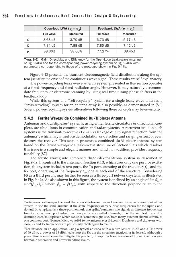
394 F r o n t i e r s i n a n t e n n a s : N e x t G e n e r a t i o n D e s i g n & e n g i n e e r i n g C h a p t e r 9 : L e a k y - W a v e a n t e n n a s 395
Figure 9-48 presents the transient electromagnetic field distributions along the sys-tem just after the onset of the continuous wave signal. These results are self-explanatory.
The power-recycling leaky-wave antenna system presented in this section operates at a fixed frequency and fixed radiation angle. However, it may naturally accommo-date frequency or electronic scanning by using real-time tuning phase shifters in the feedback loop.
While this system is a “self-recycling” system for a single leaky-wave antenna, a “cross-recycling” system for an antenna array is also possible, as demonstrated in [86]. Several power-recycling system alternatives following these concepts may be envisioned.
9.4.2 Ferrite Waveguide Combined Du/Diplexer AntennaAntennas and du/diplexer26 systems, using either ferrite circulators or directional cou-plers, are ubiquitous in communication and radar systems. A recurrent issue in such systems is the transmit-to-receive (Tx → Rx) leakage due to signal reflection from the antenna27, which may introduce demodulation or detection and ranging errors, or even destroy the receiver. This section presents a combined du/diplexer-antenna system based on the ferrite waveguide leaky-wave structure of Section 9.3.3 which resolves this issue in a simple and elegant manner and which, in addition, provides frequency tunability [87].
The ferrite waveguide combined du/diplexer-antenna system is described in Fig. 9-49. In contrast to the antenna of Section 9.3.3, which uses only one port for excita-tion, this system includes two ports, the Tx port,operating at the frequency fTx, and the Rx port, operating at the frequency fRx, one at each end of the structure. Considering FS as a third port, it may further be seen as a three-port network system, as illustrated in Fig. 9-49a. As also shown in this figure, the system is inclined by an angle of q = qTx = sin-1(bTx/k0), where bTx = b( fTx), with respect to the direction perpendicular to the
26A duplexer is a three-port network that allows the transmitter and receiver in a radar or communications system to use the same antenna at the same frequency or very close frequencies for the uplink and downlink. A diplexer is a three-port network that splits/combines two signals at different frequencies from/to a common port into/from two paths, also called channels; it is the simplest form of a demultiplexer/multiplexer, which can split/combine signals to/from many different channels from/to one common port. [Source: Microwave101 (www.microwaves101.com)]. Duplexers and diplexers with close Rx and Tx frequencies are particularly challenging to realize. 27For instance, in an application using a typical antenna with a return loss of 15 dB and a Tx power of 50 dBm, a power of 35 dBm leaks into the Rx via the circulator (neglecting its losses). Although a power limiter may be used to mitigate this problem, this approach suffers from additional insertion loss, harmonic generation and power handling issues.
Table 9-2 Gain, Directivity, and Efficiency for the Open-Loop Leaky-Wave Antenna of Fig. 9-46a and for the corresponding power-recycling system of Fig. 9-46b with parameters corresponding to those of the prototype shown in Fig. 9-47b.
Open-loop LWA (er = er0) Feedback LWA (er = ers)
Full-wave Measured Full-wave Measured
G 3.68 dB 3.70 dB 6.73 dB 5.77 dB
D 7.84 dB 7.88 dB 7.85 dB 7.42 dB
er
38.36% 38.00% 77.27% 68.45%

394 F r o n t i e r s i n a n t e n n a s : N e x t G e n e r a t i o n D e s i g n & e n g i n e e r i n g C h a p t e r 9 : L e a k y - W a v e a n t e n n a s 395
Figure 9-48 Full-wave simulated (FIT, CST Microwave Studio) transient electric field distributions for the power-recycling 3-dB LWA system of Fig. 9-47b at different instants. The excitation frequency is f = 4.58 GHz, corresponding to the harmonic period of T = 1/f = 0.218 ns. Notice the directions of phase progression indicated by the arrows.
(a) t0 = 0 ns
(d) t3 = 3T/4 = 0.301 ns (e) t4 = T = 0.519 ns (f) t5 = 8T = 1.884 ns
(c) t2 = T/2 = 0.246 ns(b) t1 = T/4 = 0.192 ns
Figure 9-49 Ferrite waveguide combined du/diplexer antenna system. (a) Configuration [using the antenna structure of Fig. 9-26a] for the case f
Tx > f
Rx. (b) Corresponding location of f
Tx and f
Rx
in the dispersion diagram of the same ferrite waveguide structure as in Fig. 9-27b. (c) Prototype with back conductor [same as that of Fig. 9-26b except for the additional port] and stub matching networks at the Tx and Rx ports.
Forwardradiation
Backwardreception
Ferrite waveguideleaky-wave antenna
θ
θ = sin−1(βTx/k0)
H0
P1:Tx
P2:Rx
P3:FS
(a)
5.6
5.8
6
6.2
–100 0 100β(rad/m)
f (G
Hz)
βRx βTx
P2
P1
k0 = −β k0 = +β
(b)
Matching Section
Waveguide structure (open side)
NdFeB magnet
P2 P1
(c)

396 F r o n t i e r s i n a n t e n n a s : N e x t G e n e r a t i o n D e s i g n & e n g i n e e r i n g C h a p t e r 9 : L e a k y - W a v e a n t e n n a s 397
direction of radiation, if fTx > fRx; conversely, the angle is q = qRx = sin-1(bRx/k0) if fTx < fRx. In the former case ( fTx > fRx ), which is illustrated in Fig. 9-49a, the Tx signal is radiated in the forward (RH) quadrant of the antenna and the signal incoming from FS is picked up by Rx in the backward (LH) quadrant of the antenna; the converse holds in the other case (fTx < fRx). In both cases, bRx = -bTx, as shown in Fig. 9-49b, so that qRx = -qTx, ensuring that the beams point to the direction perpendicular to the ground for both the Tx and Rx operations. When fTx ≠ fRx, the system operates as a diplexer, and requires an inclina-tion angle with respect to the ground. In the particular case fTx = fRx, it operates as a duplexer, and is set parallel to the ground. Figure 9-50 plots the required inclination angle of the system as a function of the separation frequency ∆ f = fTx - fRx.
The Tx signal is radiated by the leaky-wave antenna as in the antenna of Section 9.3.3. By virtue of the leaky-wave radiation mechanism, the structure may be designed long enough such that all of the Tx signal power has radiated out of the structure before reaching the Rx port on the other side, thereby automatically preventing any Tx → Rx leakage and providing large Tx → Rx isolation. Moreover, the incoming RF signal picked up by the antenna can only propagate toward the Rx port due to the nonreciproc-ity of the structure (Fig. 9-27), and therefore extremely high RF → Tx isolation is auto-matically achieved. The antenna can thus simultaneously transmit and receive without any interference or leakage between the Tx and Rx signals. Thus, it constitutes an excel-lent system with excellent du/diplexer properties, since a single antenna simultane-ously performs the Tx and Rx operations with perfect isolation. Moreover, the opera-tion frequencies of the system may be tuned by simply varying the magnetic bias field, and unwanted symmetric (-q0 with respect to q0) beams caused by termination reflec-tions are automatically suppressed both at Tx and Rx.
Figures 9-51a and 9-51b show the main scattering parameters obtained by full-wave simulation and experiment, respectively. The diplexing Tx and Rx frequencies
Figure 9-50 Required inclination angle q versus ∆f = fTx - f
Rx for the system of Fig. 9-49a,
computed from the dispersion diagram of Fig. 9-27b.
–80
–60
–40
–20
0
20
40
60
80
–0.4 –0.2 0 0.2 0.4
∆f = fTx − fRx (GHz)
Incl
inat
ion
angl
e θ
(deg
)
fTx = fRx(duplexing)
fTx > fRx(diplexing)
fTx < fRx(diplexing)
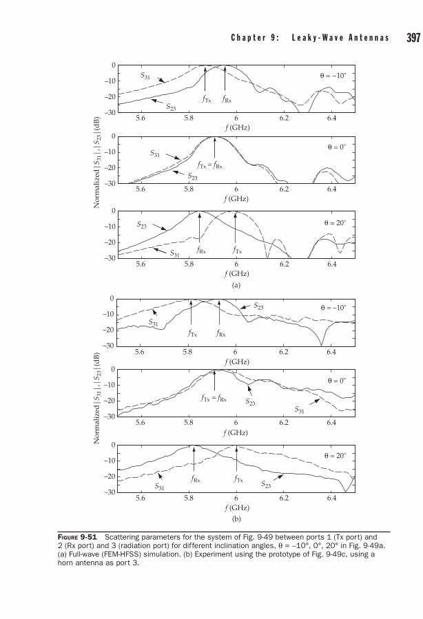
396 F r o n t i e r s i n a n t e n n a s : N e x t G e n e r a t i o n D e s i g n & e n g i n e e r i n g C h a p t e r 9 : L e a k y - W a v e a n t e n n a s 397
Figure 9-51 Scattering parameters for the system of Fig. 9-49 between ports 1 (Tx port) and 2 (Rx port) and 3 (radiation port) for different inclination angles, q = -10°, 0°, 20° in Fig. 9-49a. (a) Full-wave (FEM-HFSS) simulation. (b) Experiment using the prototype of Fig. 9-49c, using a horn antenna as port 3.
–30
–20
–10
0
–30
–20
–10
0
–30
–20
–10
0
–30
–20
–10
0
–30
–20
–10
0
5.6
–30
–20
–10
0
f (GHz)
f (GHz)
f (GHz)
Nor
mal
ized
|S 3
1|,|
S 23|
(dB
)N
orm
aliz
ed|
S 31|
,|S 2
3|(d
B)
θ = 0˚
θ = 20˚
θ = –10˚
θ = 0˚
θ = 20˚
θ = −10˚
S23
S23
S23
S31
S31
S31
fTx
fTx
fRx
fRx
fTx = fRx
(a)
5.6 5.8 6 6.2 6.4f (GHz)
f (GHz)
f (GHz)
S23
S23
S23
S31
S31
S31
fTx
fTx
fRx
fRx
fTx = fRx
(b)
6.46.265.8
5.6 6.46.265.8
5.6 6.46.265.8
5.6 6.46.265.8
5.6 6.46.265.8

398 F r o n t i e r s i n a n t e n n a s : N e x t G e n e r a t i o n D e s i g n & e n g i n e e r i n g C h a p t e r 9 : L e a k y - W a v e a n t e n n a s 399
Figure 9-52 Active beam-forming leaky-wave antenna concept
z
ψ(z)
Tunable amplifiers
ψbinomial
ψuniform
Leaky-wave antenna
agree well with the dispersion diagram predictions of Fig. 9-50. Other relevant scatter-ing parameters (not shown) are: |S21/S12|= 40 dB (Tx-Rx/Rx-Tx isolation), |S31/S13| = 15 dB (Tx-RF/RF-Tx discrimination), |S23/S32|= 17 dB (RF-Rx/Rx-RF discrimination), and |S23/S13| = 15 dB (RF-Rx/RF-Tx discrimination).
The concept of the du/diplexer-antenna system presented in this section was recently extented to a novel integrated front-end [88]. This front-end is capable of full-space beam-scanning using magnetic bias tuning at fixed RF and LO frequencies. By setting the RF signal frequency in the CRLH leaky-wave region of the structure and the LO signal frequency in the edge-mode guided-wave region of the structure, this co-designed system uses the ferrite waveguide structure simultaneously as the radiator and as the power combiner for first-stage mixing.
9.4.3 Active Beam-Shaping AntennaDue to the subwavelength nature of metamaterial unit cells ( p << lg), low-gain tunable amplifiers may be conveniently integrated along CRLH leaky-wave antenna structures to manipulate the magnitude of the signal along it, in addition to its phase, and thereby control its leakage constant for beam forming. This operation may be performed in real time using voltage controlled amplifiers. The concept is illustrated in Fig. 9-52. The field on the aperture of the antenna is “digitized,” namely discretized along the axis of propagation (z direction) at the location of the amplifiers and quantized, following the exponential decay response of the leaky-wave radiating sections between the amplifiers, with the magnitude controlled by amplifiers with different and tunable gains. Since the radiation pattern of an aperture antenna is the Fourier transform of its aperture field distribution [7], the shape of the radiation pattern of the antenna can be controlled by approximating appropriate aperture distributions, as illustrated in Fig. 9-52. Of note is that the imperfectness of the field distribution tends to be smoothed out by the low-pass effect of the far-field Fourier integral, so that even relatively rough approxima-tions yield radiation patters which are undistinguishable from those corresponding of the ideal field distributions down to very low power levels.
Exploiting this opportunity, an active CRLH leaky-wave antenna with distributed amplifiers playing the roles of power repeaters was demonstrated in [89]. Since the

398 F r o n t i e r s i n a n t e n n a s : N e x t G e n e r a t i o n D e s i g n & e n g i n e e r i n g C h a p t e r 9 : L e a k y - W a v e a n t e n n a s 399
limitation of the effective aperture of the resulting antenna is suppressed by the repeaters, extremely high directivities are achievable by such a system, still using a simple transmission line excitation, leading to a system that is much more compact than conventional antenna arrays with their complex and lossy corporate feeding net-works. The antenna of [89] is shown in Fig. 9-53a and its performances are presented in Fig. 9-53b. A dramatic gain enhancement of 8.3 dB compared to the case of a passive antenna is easily achieved. This enhancement is naturally due to the increased directiv-ity of the structure, but also to an increased efficiency due to the cancelation of cell reflections resulting from the unilateral nature of the amplifiers.
The active system of Fig. 9-53 is designed for a uniform field distribution. However, this distribution may naturally be reconfigured in real time by variable-gain amplifiers in a more sophisticated system. The beam-forming performance of such a system is shown in shown in Fig. 9-54, where the radiation patterns for uniform and binomial distributions are compared.
CRLH leaky-wave structures incorporating active elements may lead to quasi-“universal” smart antenna systems. Such systems might perform simultaneously
Figure 9-53 Active leaky-wave antenna with increased (uniform) aperture for enhanced directivity. The antenna is designed for broadside radiation. (a) Antenna prototype. The structure is made of two back-to-back microstrip structures. The top substrate layer supports the radiative part, which includes 8 CRLH leaky-wave antennas of the type shown in Fig. 9-18b. The bottom substrate layer supports the amplifying part, which includes 7 amplifiers placed on 360° phase-shifting loops ensuring a uniform phase distribution for broadside radiation. The two layers are interconnected by plated vias passing through slots opened in the contacting ground planes of the two substrates. (b) Radiation pattern at 3.7 GHz for the antenna shown in (a).
(a)
–10 dB
0 dB
Passive AF th.
Active AF th.Active meas.
Top radiating layer
Bottom amplifying layer
Passive full-wave
Gmeas = 17.2 dBactive
Gfull-wave = 8.9 dBpassive
(b)
60º
30º
Figure 9-54 Beam shaping achieved by a CRLH active leaky-wave antenna with the same passive parameters as the structure shown in Fig. 9-53a for the two aperture digitized fields shown in Fig. 9-52, i.e., uniform for maximal directivity and binomial for minimal sidelobe level.
Uniform Binomial0º 0º
30º 30º
60º 60º
–10 dB –10 dB
–20 dB3UCs/SC
HPBW = 15.4ºSLL = –∞ dB
0 dB 0 dB
3UCs/SCHPBW = 6.4º
SLL = –12.7 dB
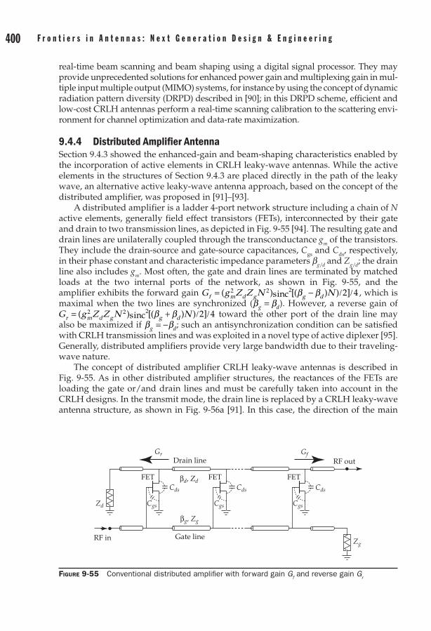
400 F r o n t i e r s i n a n t e n n a s : N e x t G e n e r a t i o n D e s i g n & e n g i n e e r i n g C h a p t e r 9 : L e a k y - W a v e a n t e n n a s 401
real-time beam scanning and beam shaping using a digital signal processor. They may provide unprecedented solutions for enhanced power gain and multiplexing gain in mul-tiple input multiple output (MIMO) systems, for instance by using the concept of dynamic radiation pattern diversity (DRPD) described in [90]; in this DRPD scheme, efficient and low-cost CRLH antennas perform a real-time scanning calibration to the scattering envi-ronment for channel optimization and data-rate maximization.
9.4.4 Distributed Amplifier AntennaSection 9.4.3 showed the enhanced-gain and beam-shaping characteristics enabled by the incorporation of active elements in CRLH leaky-wave antennas. While the active elements in the structures of Section 9.4.3 are placed directly in the path of the leaky wave, an alternative active leaky-wave antenna approach, based on the concept of the distributed amplifier, was proposed in [91]–[93].
A distributed amplifier is a ladder 4-port network structure including a chain of N active elements, generally field effect transistors (FETs), interconnected by their gate and drain to two transmission lines, as depicted in Fig. 9-55 [94]. The resulting gate and drain lines are unilaterally coupled through the transconductance gm of the transistors. They include the drain-source and gate-source capacitances, Cgs and Cds, respectively, in their phase constant and characteristic impedance parameters bg / d and Zg / d; the drain line also includes gm. Most often, the gate and drain lines are terminated by mat ched loads at the two internal ports of the network, as shown in Fig. 9-55, and the amplifier exhibits the forward gain G g Z Z N Nf m d g g d= - / /( ) [( ) ) ]2 2 2 2 4sinc b b , which is maximal when the two lines are synchronized (b bg d= ). However, a reverse gain of G g Z Z N Nr m d g g d= + / /( ) [( ) ) ]2 2 2 2 4sinc b b toward the other port of the drain line may also be maximized if b bg d= - ; such an antisynchronization condition can be satisfied with CRLH transmission lines and was exploited in a novel type of active diplexer [95]. Generally, distributed amplifiers provide very large bandwidth due to their traveling-wave nature.
The concept of distributed amplifier CRLH leaky-wave antennas is described in Fig. 9-55. As in other distributed amplifier structures, the reactances of the FETs are loading the gate or/and drain lines and must be carefully taken into account in the CRLH designs. In the transmit mode, the drain line is replaced by a CRLH leaky-wave antenna structure, as shown in Fig. 9-56a [91]. In this case, the direction of the main
Figure 9-55 Conventional distributed amplifier with forward gain Gf and reverse gain G
r
Zd
RF in
RF out
Zg
GfGr
FETFETFET
Drain line
Gate line
βd, Zd
βg, Zg
CgsCgsCgs
CdsCdsCds

400 F r o n t i e r s i n a n t e n n a s : N e x t G e n e r a t i o n D e s i g n & e n g i n e e r i n g C h a p t e r 9 : L e a k y - W a v e a n t e n n a s 401
beam is determined by the dispersion diagram of the CRLH drain line. In contrast, a receive mode system is realized if it is the gate line that is replaced by the CRLH struc-ture, as shown in Fig. 9-56b [92]. In this case, if a wave incident from one quadrant of space is at a frequency in the RH region, a RH wave is generated that is forwardly amplified to the corresponding port with the forward gain Gf . On the other hand, if the frequency of the incident wave is in the LH region, a LH wave is generated that is reversely amplified to the other port with the reverse gain Gr , as illustrated in Fig. 9-56b. If both the gate and the drain lines are replaced by CRLH antennas, the system receives the signal with the gate antenna and re-radiates it with the drain antenna in the direc-tion symmetrically opposite to that of the incident wave; this system might be used as a repeater or transponder [93]. In all the cases, the CRLH antenna Tx or Rx angles fol-low the classical scanning law, q0 = sin-1(b/k0), where b = bd or b = bg.
Figure 9-57a shows a transmit-mode microstrip distributed amplifier CRLH leaky-wave antenna prototype. The input signal on the microstrip line is periodically tapped and fed to the gates of the FETs. The outputs of the FETs are next combined in the
Drain line
Gate line
CRLH ant.
VTx
(a)
Drain line
Gate line
CRLH ant.
ZRxRH
Gf (RH)
ZRxLH
Gr (LH)
(b)
Figure 9-56 Conceptual description of the distributed amplifier CRLH leaky-wave antenna. The systems are the same as that shown in Fig. 9-55 except that one of the transmission lines has been replaced by a CRLH leaky-wave antenna. (a) Transmit (Tx) mode, using a CRLH drain line antenna. (b) Receive (Rx) mode, using a CRLH gate line antenna.
Figure 9-57 Tx-mode microstrip distributed amplifier CRLH leaky-wave antenna (corresponding to the case of Fig. 9-56a). (a) Prototype. (b) Corresponding frequency-scanning radiation patterns.
#1
#3
Equal lengthcoupling lines#4
13 mm
FETs
CRLH antenna
PREV
#2 P
PFWD
Pin
Gate line
Drain line/antenna
(a)
–20
–10
0
10
–90Angle [deg]
[dB
i]
(b)
90450–45
1.8 GHz 2 GHz 2.2 GHz2.4 GHz 2.6 GHz 2.8 GHz
3 GHz 3.2 GHz 3.4 GHz
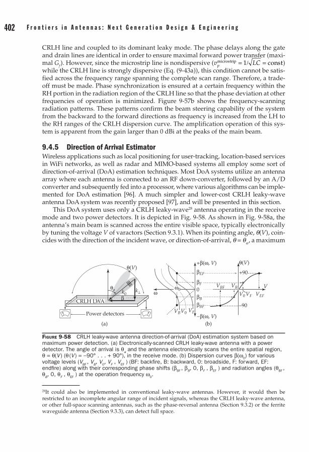
402 F r o n t i e r s i n a n t e n n a s : N e x t G e n e r a t i o n D e s i g n & e n g i n e e r i n g C h a p t e r 9 : L e a k y - W a v e a n t e n n a s 403
CRLH line and coupled to its dominant leaky mode. The phase delays along the gate and drain lines are identical in order to ensure maximal forward power transfer (maxi-mal Gf ). However, since the microstrip line is nondispersive (v LCp
microstrip const= / = .1 ) while the CRLH line is strongly dispersive (Eq. (9-43a)), this condition cannot be satis-fied across the frequency range spanning the complete scan range. Therefore, a trade-off must be made. Phase synchronization is ensured at a certain frequency within the RH portion in the radiation region of the CRLH line so that the phase deviation at other frequencies of operation is minimized. Figure 9-57b shows the frequency-scanning radiation patterns. These patterns confirm the beam steering capability of the system from the backward to the forward directions as frequency is increased from the LH to the RH ranges of the CRLH dispersion curve. The amplification operation of this sys-tem is apparent from the gain larger than 0 dBi at the peaks of the main beam.
9.4.5 Direction of Arrival EstimatorWireless applications such as local positioning for user-tracking, location-based services in WiFi networks, as well as radar and MIMO-based systems all employ some sort of direction-of-arrival (DoA) estimation techniques. Most DoA systems utilize an antenna array where each antenna is connected to an RF down-converter, followed by an A/D converter and subsequently fed into a processor, where various algorithms can be imple-mented for DoA estimation [96]. A much simpler and lower-cost CRLH leaky-wave antenna DoA system was recently proposed [97], and will be presented in this section.
This DoA system uses only a CRLH leaky-wave28 antenna operating in the receive mode and two power detectors. It is depicted in Fig. 9-58. As shown in Fig. 9-58a, the antenna’s main beam is scanned across the entire visible space, typically electronically by tuning the voltage V of varactors (Section 9.3.1). When its pointing angle, q(V), coin-cides with the direction of the incident wave, or direction-of-arrival, q = qa , a maximum
θa
θ(V)
k0β
k⊥
Power detectors
(a)
CRLH LWA
+90
–90
ωω0
VBV0 VF
βEF
βF
0βB
βBF
+β(ω, V)
−β(ω, V)
VBF
VEF
VB
VFV0
θ(V)
V
(b)
Figure 9-58 CRLH leaky-wave antenna direction-of-arrival (DoA) estimation system based on maximum power detection. (a) Electronically-scanned CRLH leaky-wave antenna with a power detector. The angle of arrival is q
a and the antenna electronically scans the entire spatial region,
q = q(V ) (q (V ) = -90° . . . + 90°), in the receive mode. (b) Dispersion curves b(w0) for various
voltage levels (VBF
, VB, V
0, V
F , V
EF ) (BF: backfire, B: backward, 0: broadside, F: forward, EF:
endfire) along with their corresponding phase shifts (bBF
, bB, 0, b
F , b
EF ) and radiation angles (q
BF ,
qB, 0, q
F , q
EF ) at the operation frequency w
0.
28It could also be implemented in conventional leaky-wave antennas. However, it would then be restricted to an incomplete angular range of incident signals, whereas the CRLH leaky-wave antenna, or other full-space scanning antennas, such as the phase-reversal antenna (Section 9.3.2) or the ferrite waveguide antenna (Section 9.3.3), can detect full space.

402 F r o n t i e r s i n a n t e n n a s : N e x t G e n e r a t i o n D e s i g n & e n g i n e e r i n g C h a p t e r 9 : L e a k y - W a v e a n t e n n a s 403
of power is coupled into the antenna, as a result of phase matching on its surface (ba = b, ba: tangential component of the incident wave vector, b: phase constant of the antenna dictated by its dispersion relation), and the resulting maximum of power measured by one of the detectors indicates the sought angle using the known scanning law of the antenna, illustrated in Fig. 9-58b.
In principle only one detector, placed at either end of the antenna (the other end being terminated by a matched load), would suffice. However, to relax the constraints on the required voltage swing of the varactors, and to reduce the associated losses, the two-detector system represented in Fig. 9-58a is practically preferable. This system may use either of the two modes represented in Fig. 9-59. The direction of the propagation vec-tor b (or phase velocity) along the antenna structure always corresponds to the direction of ba . In contrast, the direction of the pointing vector S along the surface is dictated by the regime of the CRLH antenna: it is the same as the direction of b in the RH regime and opposite to the direction of b in the LH regime. Since the direction of S indicates the direc-tion of power flow, the maximum power will be transmitted to the direction indicated by S, as shown in Fig. 9-59. Whether the antenna is operating in the RH or the LH regime, the quadrant of the incident wave is determined by the sign of the power difference between the two detectors, ∆P = PD1 - PD2, while the DoA estimation is obtained from its peak value.29 Figure 9-59 shows the four possible scenarios, two of them existing for each mode of operation.
29As with every antenna, the antenna’s gain varies with the scanning angle. As the DoA estimation system proposed here is contingent on measuring the received power, which is a function of the antenna’s gain, a variable-gain antenna might present limitations regarding the accuracy of this system. However, the antenna’s gain may be equalized in the receiver from the known gain vs. angle characteristic of the antenna. This equalization consists de facto in normalizing the radiation patterns of all angles to the most achievable maximum by adding a correction factor so as to obtain a constant gain versus scan angle. In this manner, the received power is no longer a function of the antenna’s gain, but only of the scan angle. The correction factors can thus be applied in DSP once all of the received powers have been measured for all the scan angles.
Figure 9-59 DoA estimation forward and backward modes, both possible for signals incoming from either the right or left quadrants.
Max
imum
Pow
er D
etec
tion
Pow
er d
etec
tor
1Po
wer
det
ecto
r 2
Mode #1: VF only(0º→ + 90º)
Mode #2: VB only(0º→ – 90º)
Differental power P = PD1 – PD2
MAXPD1
MINPD2
S
#1
SMAXPD2
MINPD1
#2
MAXPD1
MINPD2
S
#3
−90º
−90º
0º 0º
+90º
0º 0º
0º
+90º
SMAXPD2
MINPD1
#4
0º 90º
Max
90º
Max
θa
θa
θaθa
θa θa
αα
α α
θ
VF = Forward voltage θa = Incident angleVB = Backward voltageLegend:

404 F r o n t i e r s i n a n t e n n a s : N e x t G e n e r a t i o n D e s i g n & e n g i n e e r i n g C h a p t e r 9 : L e a k y - W a v e a n t e n n a s 405
Figure 9-60 shows the full-wave simulated Poynting vector for the DoA system in receive mode. In this numerical simulation, a plane wave is incident on the antenna at an angle of qa, and the power detectors PD1 and PD2 are represented by two-dimensional planar surfaces perpendicular to the direction of propagation at the two ports, over which the Poynting vector is integrated to obtain the total outflowing power. These electromagnetic results clearly show that the power propagation along the antenna fol-lows the scheme of Fig. 9-59.
Figure 9-61 shows the differential power results from the full-wave simulations for all four scenarios in Fig. 9-59. For scenarios #1 and #2, the incident angle is qa = 28° from
Figure 9-60 Full-wave (FEM-HFSS) simulation results verifying the direction of power flow (Poynting vector S) in the DoA system of Fig. 9-58. (a) Scenario #3 (LH/backward mode) with q
a = -31° in Fig. 9-59: the phase (b
x ) progresses toward PD2 while S points toward PD1.
(b) Scenario #2 (RH/forward modes) with qa = 28° in Fig. 9-58: the phase (b
x ) progresses
toward PD2 and S points toward PD2.
z
k0kz
S
β βPD1
PD2
LH/FWD modeθa = –31º
(a)
z
k0kz
S
θa = 28º
PD1
RH/FWD mode
PD2
(b)
Figure 9-61 DoA estimation results (crosses represent recorded results and solid line represents the fitting function) based on full-wave (FEM-HFSS) simulations. Scenarios #1–#4 correspond to the same scenarios in Fig. 9-59.
10
1
0.8
0.6
0.4
0.2
−1
−0.8
−0.6
−0.4
−0.2−70 −60 −50 −40 −30 −20 −10
#3
#4
#1
#2
θa = 28º, DoA = 28º θa = –31º, DoA = –31º
Left-handed/backward mode
Right-handed/forward mode
Angle of Arrival θºAngle of Arrival θº
706050403020
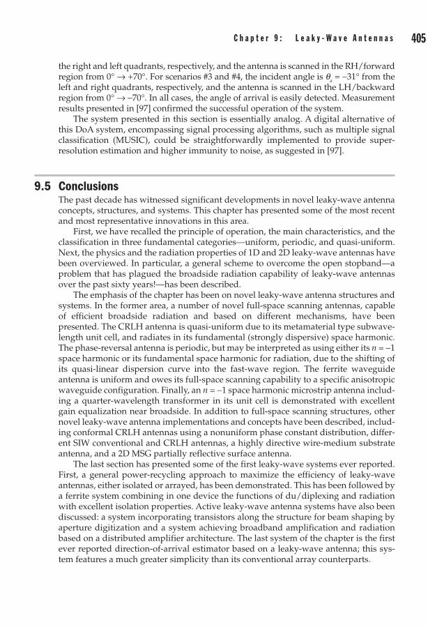
404 F r o n t i e r s i n a n t e n n a s : N e x t G e n e r a t i o n D e s i g n & e n g i n e e r i n g C h a p t e r 9 : L e a k y - W a v e a n t e n n a s 405
the right and left quadrants, respectively, and the antenna is scanned in the RH/forward region from 0° → +70°. For scenarios #3 and #4, the incident angle is qa = -31° from the left and right quadrants, respectively, and the antenna is scanned in the LH/backward region from 0° → -70°. In all cases, the angle of arrival is easily detected. Measurement results presented in [97] confirmed the successful operation of the system.
The system presented in this section is essentially analog. A digital alternative of this DoA system, encompassing signal processing algorithms, such as multiple signal classification (MUSIC), could be straightforwardly implemented to provide super-resolution estimation and higher immunity to noise, as suggested in [97].
9.5 ConclusionsThe past decade has witnessed significant developments in novel leaky-wave antenna concepts, structures, and systems. This chapter has presented some of the most recent and most representative innovations in this area.
First, we have recalled the principle of operation, the main characteristics, and the classification in three fundamental categories—uniform, periodic, and quasi-uniform. Next, the physics and the radiation properties of 1D and 2D leaky-wave antennas have been overviewed. In particular, a general scheme to overcome the open stopband—a problem that has plagued the broadside radiation capability of leaky-wave antennas over the past sixty years!—has been described.
The emphasis of the chapter has been on novel leaky-wave antenna structures and systems. In the former area, a number of novel full-space scanning antennas, capable of efficient broadside radiation and based on different mechanisms, have been presented. The CRLH antenna is quasi-uniform due to its metamaterial type subwave-length unit cell, and radiates in its fundamental (strongly dispersive) space harmonic. The phase-reversal antenna is periodic, but may be interpreted as using either its n = -1 space harmonic or its fundamental space harmonic for radiation, due to the shifting of its quasi-linear dispersion curve into the fast-wave region. The ferrite waveguide antenna is uniform and owes its full-space scanning capability to a specific anisotropic waveguide configuration. Finally, an n = -1 space harmonic microstrip antenna includ-ing a quarter-wavelength transformer in its unit cell is demonstrated with excellent gain equalization near broadside. In addition to full-space scanning structures, other novel leaky-wave antenna implementations and concepts have been described, includ-ing conformal CRLH antennas using a nonuniform phase constant distribution, differ-ent SIW conventional and CRLH antennas, a highly directive wire-medium substrate antenna, and a 2D MSG partially reflective surface antenna.
The last section has presented some of the first leaky-wave systems ever reported. First, a general power-recycling approach to maximize the efficiency of leaky-wave antennas, either isolated or arrayed, has been demonstrated. This has been followed by a ferrite system combining in one device the functions of du/diplexing and radiation with excellent isolation properties. Active leaky-wave antenna systems have also been discussed: a system incorporating transistors along the structure for beam shaping by aperture digitization and a system achieving broadband amplification and radiation based on a distributed amplifier architecture. The last system of the chapter is the first ever reported direction-of-arrival estimator based on a leaky-wave antenna; this sys-tem features a much greater simplicity than its conventional array counterparts.

406 F r o n t i e r s i n a n t e n n a s : N e x t G e n e r a t i o n D e s i g n & e n g i n e e r i n g C h a p t e r 9 : L e a k y - W a v e a n t e n n a s 407
References A. Hessel, [1] Antenna Theory, Part II, R. E. Collin and R. F. Zucker, Eds. New York: McGraw-Hill, 1969, chap. 19.T. Tamir, [2] Antenna Theory, Part II, R. E. Collin and R. F. Zucker, Eds. New York: McGraw-Hill, 1969, chap. 20.A. A. Oliner, and D. R. Jackson, [3] Antenna Engineering Handbook, 4th ed., J. Volakis, Ed. New York: McGraw-Hill, 2007.D. R. Jackson, and A. A. Oliner, [4] Modern Antenna Handbook, C. A. Balanis, Ed. Wiley-Interscience, 2008.W. W. Hansen, “Radiating electromagnetic waveguide,” Patent, 1940, U.S. Patent No. 2.402.622.[5] F. J. Zucker, [6] Antenna Engineering Handbook, 4th ed., J. L. Volakis, Ed. New York: McGraw-Hill, 2007, chap. 10.J. D. Krauss, and R. J. Marhefka, [7] Antennas for All Applications, 3rd ed. New York: McGraw-Hill, 2001.W. Menzel, “A new traveling-wave antenna in microstrip,” [8] Archiv fur Elek-tronik und Ubertragungstechnik (AEU), vol. 33, no. 4, pp. 137–140, April 1979.A. A. Oliner, “Leakage from higher modes on microstrip line with applica tions to antennas,” [9] Radio Science, vol. 22, no. 6, pp. 907–912, Nov. 1987.L. Brillouin, [10] Wave Propagation in Periodic Structures. New York: Dover Publications, 1946.J. N. Hines, “A wide aperture tapered-depth scanning antenna,” Ohio State Univ. Res. Found., [11] Columbus, OH, Tech. Rep. 667–7, Dec. 1957.R. C. Honey, “A flush-mounted leaky wave antenna with predictable pat terns,” [12] IRE Trans. Antennas Propagat, vol. AP-7, pp. 320–329, Oct. 1959.C. H. Walter, [13] Traveling Wave Antennas. New York: McGraw-Hill, 1969.R. F. Harrington, [14] Time Harmonic Electromagnetic Fields. New York: Wiley & IEEE Press, 2001.H. Shigesawa, M. Tsuji, and A. A. Oliner, “The nature of the spectral-gap between bound and leaky [15] solutions,” Radio Sci., vol. 28, no. 6, pp. 1235–1243, Nov.–Dec. 1993.C. Balanis, [16] Antenna Theory: Analysis and Design, 3rd ed. New York: Wiley, 2005.G. Lovat, P. Burghignoli, and D. R. Jackson, “Fundamental properties and optimization of broad-[17] side radiation from uniform leaky-wave antennas,” IEEE Trans. Antennas Propagat, vol. 54, no. 5, pp. 1442–1452, May 2006.A. A. Oliner, “Radiating periodic structures: analysis in terms of [18] k vs. b diagrams,” Polytechnic Institute of Brooklyn (now Polytechnic University), Tech. Rep., 1963.–––––, “Scannable millimeter wave arrays,” Polytechnic University, Tech. Rep., 1988.[19] S. Paulotto, P. Baccarelli, F. Frezza, and D. R. Jackson, “Full-wave modal dispersion analysis and [20] broadside optimization for a class of mi-crostrip CRLH leaky-wave antennas,” IEEE Trans. Microwave Theory Tech., vol. 56, no. 12, pp. 2826–2837, Dec. 2008.P. Baccarelli, S. Paulotto, D. R. Jackson, and A. A. Oliner, “A new bril louin dispersion diagram for [21] 1-D periodic printed structures,” IEEE Trans. Microwave Theory Tech., vol. 55, no. 7, pp. 1484–1495, July 2007.L. Liu, C. Caloz, and T. Itoh, “Dominant mode (DM) leaky-wave antenna with backfire-to-endfire [22] scanning capability,” Electron. Lett., vol. 38, no. 23, pp. 1414–1416, Nov. 2002.C. Caloz, and T. Itoh, [23] Electromagnetic Metamaterials: Transmission Line Theory and Microwave Applications. Hoboken: Wiley & IEEE Press, 2006.D. M. Pozar, [24] Microwave Engineering, 3rd ed. Hoboken: Wiley, 2004.R. S. Elliot, [25] Antenna Theory and Design. Englewood Cliffs: Prentice-Hall. 1981.P. Burghignoli, G. Lovat, and D. R. Jackson, “Analysis and optimization of leaky-wave radiation [26] at broadside from a class of 1-D periodic structures,” IEEE Trans. Antennas Propagat, vol. 54, no. 9, pp. 2593–2603, Sept. 2006.A. Ip, and D. R. Jackson, “Radiation from cylindrical leaky waves,” [27] IEEE Trans. Antennas Propagat., vol. 38, no. 4, pp. 482–488, April 1990.C. A. Allen, C. Caloz, and T. Itoh, “A novel metamaterial-based two-dimensional conical-beam [28] antenna,” in IEEE MTT-S Intl. Microwave Symp., Fort Worth, June 2004.C. A. Allen, K. M. K. H. Leong, C. Caloz, and T. Itoh, “A two-dimensional edge excited metamaterial-[29] based leaky-wave antenna,” in IEEE AP-S Intl. Symp., Washington, June 2005.C. Caloz, and T. Itoh, “Array factor approach of leaky-wave antennas and application to 1D/2D [30] composite right/left-handed (CRLH) structures,” IEEE Microwave Wireless Compon. Lett., vol. 14, no. 6, pp. 274–276, June 2004.C. Caloz, T. Itoh, and A. Rennings, “CRLH metamaterial leaky-wave and resonant antennas,” [31] IEEE Antennas Propagat. Mag., vol. 50, no. 5, pp. 25–39, Oct. 2008.

406 F r o n t i e r s i n a n t e n n a s : N e x t G e n e r a t i o n D e s i g n & e n g i n e e r i n g C h a p t e r 9 : L e a k y - W a v e a n t e n n a s 407
S. Lim, C. Caloz, and T. Itoh, “Metamaterial-based electronically con trolled transmission line struc-[32] ture as a novel leaky-wave antenna with tun able angle and beamwidth,” IEEE Trans. Microwave Theory Tech., vol. 53, no. 1, pp. 161–173, Jan. 2005.–––––, “A refiecto-directive system using a composite right/left-handed (CRLH) leaky-wave [33] antenna and heterodyne mixing,” IEEE Microwave Wireless Compon. Lett, vol. 14, no. 4, pp. 183–185, April 2004.C. S. Franklin, “Improvements in wireless telegraph and telephone aerials,” Patent, 1924, British [34] Patent No. 242.342.N. Yang, C. Caloz, and K. Wu, “Fixed-beam frequency-tunable phase-reversal coplanar stripline [35] antenna array,” IEEE Trans. Antennas Propa gat, vol. 57, no. 3, pp. 671–681, March 2009.–––––, “Full-space scanning periodic phase-reversal leaky-wave antenna,” [36] IEEE Trans. Microwave Theory Tech., vol. 58, no. 10, pp. 2619–2632, Oct. 2010. M. E. Hines, “Reciprocal and nonreciprocal model of propagation in ferrite stripline and microstrip [37] devices,” IEEE Trans. Antennas Propagat., vol. MTT-19, no. 5, pp. 442–451, May 1971.K. Araki, T. Koyama, and Y. Naito, “A new type of isolator using the edge-guided mode,” [38] IEEE Trans. Microw. Theory Tech., vol. MTT-23, no. 3, p. 321, March 1975.T. Kodera, and C. Caloz, “Uniform ferrite-loaded open waveguide structure with CRLH response [39] and its application to a novel backfire-to-endfire leaky-wave antenna,” IEEE Trans. Microwave Theory Tech., vol. 57, no. 4, pp. 784–795, April 2009.B. Lax, and K. J. Button, [40] Microwave Ferrites and Ferrimagnetics. New York: McGraw-Hill, 1962.P. Baccarelli, C. Nallo, F. Frezza, A. Galli, and P. Lampariello, “Attractive features of leaky-wave [41] antennas based on ferrite-loaded open waveguides,” in IEEE AP-S Intl. Symp. Dig., vol. 2, Ottawa, July 1997, pp. 1442–1445.T. Kodera, and C. Caloz, “Dual-band full-space scanning leaky-wave an tenna based on ferrite-[42] loaded open waveguide,” IEEE Wireless Propagat. Lett., vol. 8, pp. 1202–1205, Nov. 2009.–––––, “Low-profile leaky wave electric monopole loop antenna using the [43] b = 0 regime of a ferrite-loaded open waveguide,” IEEE Trans. Antennas Propagat., vol. 58, no. 10, pp. 3165–3174, Oct. 2010.S. Paulotto, P. Baccarelli, F. Frezza, and D. R. Jackson, “Novel tech nique for open-stopband sup-[44] pression in 1-D periodic printed leaky-wave antenna,” IEEE Trans. Antennas Propagat., vol. 57, no. 7, pp. 1894–1906, July 2009.M. R. Hashemi, and T. Itoh, “Dispersion engineered metamaterial-based transmission line for con-[45] formal surface application,” in Intl. Microwave Symp., Atlanta, June 2008, pp. 331–334.–––––, “Electronically controlled metamaterial-based leaky-wave transmission-line for conformal [46] surface applications,” in Intl. Microwave Symp., Boston, June 2009, pp. 69–72.J. Hirokawa, and M. Ando, “Single-layer feed waveguide consisting of posts for plane TEM wave exci-[47] tation in parallel plates,” IEEE Trans. Microwave Theory Tech., vol. 46, no. 5, pp. 625–630, May 1998.D. Deslandes, and K. Wu, “Substrate integrated waveguide leaky-wave antenna: concept and design [48] considerations,” in Asia-Pacific Microwave Conf., Suzhou, Dec. 2005.N. Marcuvitz, [49] Waveguide Handbook. Boston: Boston Technical Publishers, 1951.F. Xu, K. Wu, and X. Zhang, “Periodic leaky-wave antenna for millimeter wave applications based [50] on substrate integrated waveguide,” IEEE Trans. Antennas Propagat, vol. 52, no. 8, pp. 340–347, Feb. 2010.J. Liu, V. R. Komanduri, and D. R. Jackson, “Substrate integrated wave guide (SIW) leaky-wave [51] antenna with transverse slots,” in URSI North American Radio Science Meeting, Charleston, June 2009.R. F. Hyneman, “Closely-spaced transverse slots in rectangular waveguide,” [52] IRE Trans. Antennas Propagat, vol. 7, pp. 335–342, Oct. 1959.I. A. Eshrah, A. A. Kishk, A. B. Yakovlev, and A. W. Glisson, “Rectangular waveguide with dielectric-[53] filled corrugations supporting backward waves,” IEEE Trans. Microwave Theory Tech., vol. 53, no. 11, pp. 3298–3304, Nov. 2005.Y. Weitsch, and T. F. Eibert, “A left-handed/right-handed leaky-wave an tenna derived from slotted [54] rectangular hollow waveguide,” in European Microwave Conf., Munich, July 2007, pp. 917–920.Y. D. Dong, and T. Itoh, “Composite right/left-handed substrate integrated waveguide leaky-wave [55] antennas,” in European Microwave Conf., Munich, Oct. 2009, pp. 276–279.F. E. Gardiol, [56] Introduction to Microwaves. London: Artech House, 1984.G. M. Zelinski, M. L. Hastriter, M. Havrilla, J. Radcliffe, A. J. Terzuoli, and G. Thiele, “FDTD analysis [57] of a new leaky traveling wave antenna,” in ACES Intl. Conf., Honolulu, April 2005.H. Jiang, R. Penno, K. M. Pasala, L. Kempel, and S. Schneider, “Broad band microstrip leaky [58] wave antenna with inhomogeneous materials,” IEEE Trans. Antennas Propagat., vol. 57, no. 5, pp. 1557–1561, May 2009.

408 F r o n t i e r s i n a n t e n n a s : N e x t G e n e r a t i o n D e s i g n & e n g i n e e r i n g C h a p t e r 9 : L e a k y - W a v e a n t e n n a s 409
J. L. Gómez Tornero, D. Can ete Rebenaque, and A. Álvarez-Melcón, “Mi crostrip leaky-wave antenna [59] with control of leakage rate and only one main beam in the azimuthal plane,” IEEE Trans. Antennas Propagat., vol. 56, no. 2, pp. 335–344, Feb. 2008.K. C. Gupta, “Narrow-beam antennas using an artificial dielectric medium with permittivity less [60] than unity,” Electron. Lett., vol. 7, no. 1, pp. 16–18, Jan. 1971.J. J. Bahl, and K. C. Gupta, “A leaky-wave antenna using an artificial dielectric medium,” [61] IEEE Trans. Antennas Propagat., vol. 22, no. 1, pp. 119–122, Jan. 1974.G. Poilasne, J. Lenormand, P. Pouliguen, K. Mahdjoubi, C. Terret, and P. Gelin, “Theoretical study of [62] interactions between antennas and metallic photonic bandgap materials,” Microwave Opt. Technol. Lett, vol. 15, no. 6, pp. 384–389, Aug. 1974.M. Thevenot, C. Cheype, A. Reineix, and B. Jecko, “Directive photonic-bandgap antennas,” [63] IEEE Trans. Microwave Theory Tech., vol. 47, no. 11, pp. 2115–2122, Nov. 1999.P. S. N. G. S. Enoch, G. Tayeb, and P. Vincent, “A metamaterial for direc tive emission,” [64] Phs. Rev. B, vol. 89, no. 21, pp. 213 902-1-4, Nov. 2002.H. Boutayeb, K. Mahdjoubi, A.-C. Tarot, and T. A. Denidni, “Directivity of an antenna embedded [65] inside a fabry-perot cavity: analysis and design,” Microwave Opt. Technol. Lett., vol. 48, no. 1, pp. 12–17, Jan. 2006.G. Lovat, P. Burghignoli, F. Capolino, D. R. Jackson, and D. R. Wilton, “Analysis of directive radia-[66] tion from a line source in a metamaterial slab with low permittivity,” IEEE Trans. Antennas Propagat., vol. 54, no. 3, pp. 1017–1030, March 2006.G. Lovat, P. Burghignoli, F. Capolino, and D. R. Jackson, “Directive leaky-wave radiation from a [67] dipole source in a wire-medium slab,” IEEE Trans. Antennas Propagat, vol. 56, no. 5, pp. 1329–1339, May 2008.P. A. Belov, R. Marqués, S. I. Maslovski, I. S. Nefedov, M. Silveirinha, C. R. Simovski, and S. A. [68] Tretyakov, “Strong spatial dispersion in wire media in the very large wavelength limit,” Phys. Rev. B, vol. 67, pp. 113103-1-4, 2003.P. A. Belov, S. A. Tretyakov, and A. J. Viitanen, “Dispersion and reflection properties of artificial [69] media formed by regular lattices of ideally conducting wires,” J. Electromag. Waves Appl, vol. 16, pp. 1153–1170, Sept. 2002.S. Ramo, J. R. Whinnery, and T. V. Duzer, [70] Fields and Waves in Commu nication Electronics, 3rd ed. New York: John Wiley & Sons, 1994.G. Lovat, P. Burghignoli, F. Capolino, and D. R. Jackson, “High directivity in low-permittivity [71] metamaterial slabs: Ray-optic vs. leaky-wave models,” Microwave Opt. Technol. Lett, vol. 48, no. 12, pp. 2542–2548, Dec. 2006.–––––, “Highly-directive planar leaky-wave antennas: A comparison between metamaterial-based [72] and conventional designs,” in European Microwave Conf., Manchester, March 2006.P. Burghignoli, G. Lovat, F. Capolino, D. R. Jackson, and D. R. Wilton, “Modal propagation and [73] excitation on a wire-medium slab,” IEEE Trans. Microwave Theory Tech., vol. 56, no. 5, pp. 1112–1124, May 2008.D. R. Jackson, and A. A. Oliner, “A leaky-wave analysis of the high-gain printed antenna configura-[74] tion,” IEEE Trans. Antennas Propagat., vol. 36, no. 7, pp. 905–910, July 1988.H. Y. Yang, and N. G. Alexopoulos, “Gain enhancement methods for printed circuit antennas through [75] multiple superstates,” IEEE Trans. Antennas Propagat, vol. AP-35, no. 7, pp. 860–863, July 1987.D. R. Jackson, A. A. Oliner, and A. Ip, “Leaky-wave propagation and radi ation for a narrow-beam [76] multiple-layer dielectric structure,” IEEE Trans. Antennas Propagat, vol. 41, no. 3, pp. 344–348, March 1993.T. Zhao, D. R. Jackson, J. T. Williams, H.-Y. D. Yang, and A. A. Oliner, “2-D periodic leaky-wave [77] antennas—part I: Metal patch design,” IEEE Trans. Antennas Propagat, vol. 53, no. 11, pp. 3505–3514, Nov. 2005.T. Zhao, D. R. Jackson, and J. T. Williams, “2-D periodic leaky-wave antennas—part II: slot design,” [78] IEEE Trans. Antennas Propagat., vol. 53, no. 11, pp. 3515–3524, Nov. 2005.R. R. DeLyser, and E. F. Kuester, “Homogenization analysis of electromag netic strip gratings,” [79] IEEE Trans. Antennas Propagat., vol. 5, no. 11, pp. 1217–1236, Nov. 1991.T. Zhao, D. R. Jackson, J. T. Williams, and A. A. Oliner, “General formulas for 2D leaky-wave anten-[80] nas,” IEEE Trans. Antennas Propagat., vol. 53, no. 11, pp. 3525–3533, Nov. 2005.–––––, “Simple CAD model for a dielectric leaky-wave antenna,” [81] IEEE Antennas Wireless Propagat. Lett, vol. 3, pp. 243–245, Dec. 2004.G. Lovat, P. Burghignoli, F. Capolino, D. R. Jackson, and D. R. Wilton, “High-gain omnidirec-[82] tional radiation patterns from a metal strip grating leaky-wave antenna,” in IEEE AP-S Intl. Symp., Honolulu, June 2007, pp. 5797–5800.

408 F r o n t i e r s i n a n t e n n a s : N e x t G e n e r a t i o n D e s i g n & e n g i n e e r i n g C h a p t e r 9 : L e a k y - W a v e a n t e n n a s 409
P. Burghignoli, G. Lovat, F. Capolino, D. R. Jackson, and D. R. Wilton, “Highly polarized, directive [83] radiation from a Fabry-Pérot ccavity leaky-wave antenna based on a metal strip grating,” IEEE Trans. Antennas Propagat., to appear.T. Zhao, “Analysis and design of 2-D periodic leaky-wave antennas using metal patches or slots,” [84] Ph.D. dissertation, University of Houston, 2003.H. V. Nguyen, A. Parsa, and C. Caloz, “Power-recycling feedback system for maximization [85] of leaky-wave antennas radiation efficiency,” IEEE Trans. Microwave Theory Tech., vol. 58, no. 7, pp. 1641–1650, July 2010.H. V. Nguyen, S. Abielmona, and C. Caloz, “Highly efficient leaky-wave antenna array using a [86] power-recycling series feeding work,” IEEE Antennas Wireless Propagat. Lett., vol. 8, pp. 441–444, March 2009.T. Kodera, and C. Caloz, “Integrated leaky-wave antenna du-plexer/diplexer using CRLH uniform [87] ferrite-loaded open waveguide,” IEEE Trans. Antennas Propagat., vol. 58, no. 8, pp. 2508–2514, Aug. 2010.–––––, “Integrated leaky-wave antenna front-end using a ferrite-loaded open waveguide structure,” [88] in European Microwave Conf., Paris, Sept. 2010, pp. 468–472.F. P. Casares-Miranda, C. Camacho-Peñalosa, and C. Caloz, “High-gain active composite right/[89] left-handed leaky-wave antenna,” IEEE Trans. An tennas Propagat, vol. 54, no. 8, pp. 2292–2300, Aug. 2006.J.-F. Frigon, C. Caloz, and Y. Y. Zhao, “Dynamic radiation pattern di versity (DRPD) mimo using [90] CRLH leaky-wave antennas,” in IEEE Radio Wireless Symp. (RWS), Orlando, Jan. 2008, pp. 743–746.K. Mori, and T. Itoh, “Distributed amplifier with CRLH-transmission line leaky wave antenna,” in [91] European Microwave Conf., Amsterdam, Oct. 2008, pp. 686–689.–––––, “CRLH metamaterial receiving leaky wave antenna integrated with distributed amplifier,” [92] in Asia Pacific Microwave Conf., Hong Kong, Dec. 2008.C. M. Wu, and T. Itoh, “A re-radiating CRLH transmission line leaky wave antenna using distributed [93] amplifiers,” in Asia Pacific Microwave Conf. Singapore, Dec. 2009.J. Beyer, S. N. Prasad, R. C. Becker, J. E. Nordman, and J. K. Hohen-warter, “Mesfet distributed [94] amplifier guidelines,” IEEE Trans. Microwave Theory Tech., vol. MTT-32, no. 3, pp. 268–275, March 1984.J. Mata-Contreras, T. M. Martín Guerrero, and C. Camacho-Peñalosa, “Experimental performance [95] of a meta-distributed amplifier,” in European Microwave Conf, Munich, Oct. 2007, pp. 743–746.L. C. Godara, “Application of antenna arrays to mobile communications, part ii: beam-forming and [96] direction-of-arrival considerations,” Proc. of the IEEE, vol. 85, no. 8, pp. 1195–1245, Aug. 1997.S. Abielmona, H. V. Nguyen, and C. Caloz, “Analog direction of arrival es timation using [97] an electronically-scanned CRLH leaky-wave antenna,” IEEE Trans. Antennas Propagat., to appear.

This page intentionally left blank
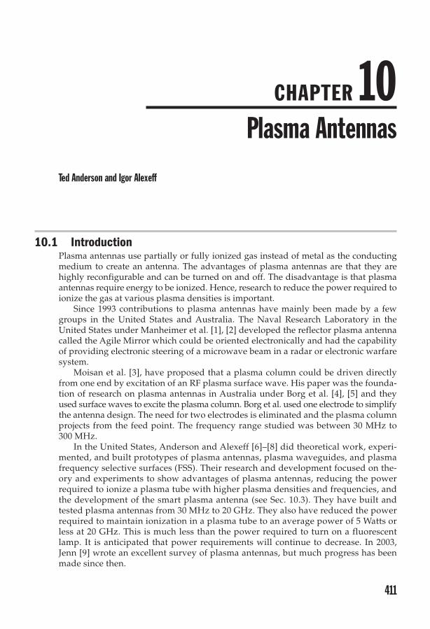
CHAPTER 10Plasma Antennas
Ted Anderson and Igor Alexeff
10.1 IntroductionPlasma antennas use partially or fully ionized gas instead of metal as the conducting medium to create an antenna. The advantages of plasma antennas are that they are highly reconfigurable and can be turned on and off. The disadvantage is that plasma antennas require energy to be ionized. Hence, research to reduce the power required to ionize the gas at various plasma densities is important.
Since 1993 contributions to plasma antennas have mainly been made by a few groups in the United States and Australia. The Naval Research Laboratory in the United States under Manheimer et al. [1], [2] developed the reflector plasma antenna called the Agile Mirror which could be oriented electronically and had the capability of providing electronic steering of a microwave beam in a radar or electronic warfare system.
Moisan et al. [3], have proposed that a plasma column could be driven directly from one end by excitation of an RF plasma surface wave. His paper was the founda-tion of research on plasma antennas in Australia under Borg et al. [4], [5] and they used surface waves to excite the plasma column. Borg et al. used one electrode to simplify the antenna design. The need for two electrodes is eliminated and the plasma column projects from the feed point. The frequency range studied was between 30 MHz to 300 MHz.
In the United States, Anderson and Alexeff [6]–[8] did theoretical work, experi-mented, and built prototypes of plasma antennas, plasma waveguides, and plasma frequency selective surfaces (FSS). Their research and development focused on the-ory and experiments to show advantages of plasma antennas, reducing the power required to ionize a plasma tube with higher plasma densities and frequencies, and the development of the smart plasma antenna (see Sec. 10.3). They have built and tested plasma antennas from 30 MHz to 20 GHz. They also have reduced the power required to maintain ionization in a plasma tube to an average power of 5 Watts or less at 20 GHz. This is much less than the power required to turn on a fluorescent lamp. It is anticipated that power requirements will continue to decrease. In 2003, Jenn [9] wrote an excellent survey of plasma antennas, but much progress has been made since then.
411

412 F r o n t i e r s i n A n t e n n a s : N e x t G e n e r a t i o n D e s i g n & E n g i n e e r i n g C h a p t e r 1 0 : P l a s m a A n t e n n a s 413
10.2 Fundamental Plasma Antenna TheoryIn the case of plasma antennas, plasma fluid models [10], [11], [12] can be used to calcu-lated plasma antenna characteristics. For example, we proceed with the derivation of net radiated power from a center-fed dipole plasma antenna with triangular current to obtain an analytical solution. For simplicity, the equations are linearized and one dimen-sion is considered with the plasma antenna dipole antenna oriented along the z-axis.
The momentum equation for electron motion in the plasma [10] is:
mddt
v e Ee j tυ υ φω+
= - - ∇( ) (10-1)
where m is the mass of the electron, u is the electron velocity in the fluid model, n is the collision rate, e is the charge on the electron, E is the electric field, w is the applied fre-quency in radians per second, and f is the electric potential.
The continuity equation for electrons in the plasma is
∂∂
+ ∂∂
=nt
nz0 0υ
(10-2)
where n is the perturbed electron density and n0 is the background plasma density.Combining the momentum equation with the continuity equation yields
njn ev j
Ez z
=-
∂∂
- ∂∂
02
2ω ωφ
( ) (10-3)
Gauss’s Law is given as
∂∂
=2
2
φεzen
(10-4)
The dielectric constant for the plasma is defined as
εω
ω ω= -
-1
2p
jv( ) (10-5)
where
ωεp
nem
=2
0 (10-6)
is the plasma frequency.Assuming the plasma antenna is a center-fed dipole antenna with a triangular cur-
rent distribution as given in Balanis [13] and substituting (10-4) , ( 10-5), and (10-6) into (10-3), and integrating over the center-fed dipole antenna, we obtain for the dipole mo-ment of the plasma antenna:
p ae n E d
m j v p
=+ -
20 0
22 ω ω ω( ) (10-7)
where a is the cross-sectional area of the plasma antenna and d is the length of the plasma antenna.

412 F r o n t i e r s i n A n t e n n a s : N e x t G e n e r a t i o n D e s i g n & E n g i n e e r i n g C h a p t e r 1 0 : P l a s m a A n t e n n a s 413
The total radiated power is then given by
Pk
cprad =
2 2
0
2
12ωπ ε
| | (10-8)
where k is the wavenumber.
Substituting equation (10-7) into equation (10-8) yields
Pa
ckd
Ep
p
rad0=
( )
-( )ε
πω
ω
ω ω
22 4 0
2
2 248( )
( )22
2 2+
ν ω. (10-9)
In this last expression we see that the net radiated power for a plasma antenna is a function of the plasma frequency and collision rates.
10.3 Plasma Antenna Windowing (Foundation of the Smart Plasma Antenna Design)
Plasma antenna windowing is a term coined to describe an RF signal being transmitted through plasma tubes, which are off or low enough in plasma density that RF signals pass through. Various designs of plasma windows appear in patents by T. Anderson [14]–[19]. Papers and conference presentations on plasma windowing have been made by T. Anderson et al. [20], [21]. A detailed numerical analysis of the performance of a reconfigurable antenna comprised of a linear omnidirectional antenna surrounded by a cylindrical shell of conducting plasma is presented. The plasma shield consists of a series of tubes containing a gas that upon electrification, forms a plasma (in practice, fluorescent lightbulbs are used). The plasma is highly conducting and acts as a reflector for radiation for frequencies below the plasma frequency. Thus, when all of the tubes surrounding the antenna are electrified, the radiation is trapped inside.
By leaving one or more of the tubes in a nonelectrified state, apertures are formed in the plasma shield, which allow radiation to escape. This is the essence of the plasma window-based reconfigurable antenna. The apertures can be closed or opened rapidly (on microsecond time scales) simply by applying voltages.
10.3.1 Theoretical Analysis with Numerical ResultsThe goal of the theoretical analysis is the prediction of the far-field radiation pattern of the plasma window antenna (PWA) for a given configuration. In order to simplify the analysis, we make the approximation that the length of the antenna and surrounding plasma tubes is irrelevant to the analysis, physically assuming that the tubes are suffi-ciently long enough that end effects can be ignored. In so doing, the problem becomes two-dimensional and as such allows for an exact solution. The problem is therefore posed as follows:
1. Assume a wire (the antenna) is located at the origin and carries a sinusoidal current of some specified frequency and amplitude.
2. Next assume that the wire is surrounded by a collection of cylindrical conductors each of the same radius and distance from the origin.
3. Solve for the field distribution everywhere in space and thus obtain the radiation pattern.

414 F r o n t i e r s i n A n t e n n a s : N e x t G e n e r a t i o n D e s i g n & E n g i n e e r i n g C h a p t e r 1 0 : P l a s m a A n t e n n a s 415
10.3.2 Geometric ConstructionOne particular configuration for the PWA is illustrated in Fig 10-1 for the case of seven cylinders. Adopt the following simple geometric construction for creating the plasma shield. For a complete shield, assume N cylinders are placed with their centers lying along a common circle chosen to have the source antenna as its center. Choose some distance from the origin d and divide the circle of radius d into equal segments subtend-ing the angles
yl = 2pl/N, (10-10)
where the integer l takes on the values l = 0, 1,…(N-1). The apertures are formed by simply excluding various cylinders from consideration.
Until this point we have considered only touching cylinders; however, there is no need to restrict our attention only to touching cylinders. In the following analysis, it is convenient to specify the cylinder radius through the use of a dimensionless parameter t, which takes on values between zero and unity (i.e., 0 ≤ t ≤ 1), where t = 0 corresponds to a cylinder of zero radius (i.e., a wire) and t = 1 corresponds to the case of touching cylinders. More explicitly, the radius of a given cylinder (all cylinder radii assumed to be equal) is given in terms of the parameter t, the distance of the cylinder to the origin d, and the number of cylinders needed for the complete shield N, by the expression
a = dt sin(p/N). (10-11)
Now define a number of geometric parameters that are needed in the analysis that follows. The coordinates specifying the center of a given cylinder are given in circular polar coordinates by (d, yl), and in Cartesian coordinates by
dl x = d cos(2pl/N) (10-12)
and
dl y = d sin(2pl/N). (10-13)
Define the displacement vector pointing from cylinder l to cylinder q by the equation
r r rd d dlq l= -q . (10-14)
The magnitude of this vector is given by
rdlq q l= - -2 1 cos( ).ψ ψ . (10-15)
The angle yl q is subtended by vectors rdq
and rdq
. In other words, if we consider the
triangle consisting of the three sides rdq ,
rdl , and
rdlq the angle yl q is the angle opposite
to the side rdlq . This angle is easily obtained by the following two relations:
d d dlq lq q q l lcos( ) cos( ) cos( )ψ ψ ψ= - (10-16)
and
d d dlq lq q q l lsin( ) sin( ) sin( ).ψ ψ ψ= - (10-17)
Lastly, define the coordinates of the observation point relative to the source as well as with respect to coordinate systems centered on the conducting cylinders. The coor-dinates of the observation point
rρ with respect to the source are denoted by (r, f).

414 F r o n t i e r s i n A n t e n n a s : N e x t G e n e r a t i o n D e s i g n & E n g i n e e r i n g C h a p t e r 1 0 : P l a s m a A n t e n n a s 415
To specify the observation point with respect to cylinder q, and define the displacement vector as
r r rρ ρq qd= - . (10-18)
The coordinates of the observation point in the system centered on cylinder q are thus (rq, fq), which are determined in the same way that the coordinates dl q and yl q were obtained above.
To complete the specification of the geometric problem, specify the coordinates of the source with respect to each of the coordinate systems centered on the cylinders. Obviously, the distance coordinate, dl s, of the source with respect to the coordinate system centered on cylinder l is given by dl q = d. The angular coordinate, yl s, is easily seen to be given by
yl s = yl + p. (10-19)
10.3.3 Electromagnetic boundary value ProblemThe solution to the boundary value problem is obtained by assuming the cylinders to be perfect conductors, which forces the electric fields to have zero tangential compo-nents on the surfaces of the cylinders. Enforcing this condition on each of the cylinders leads to N linear equations for the scattering coefficients. The consequence is an N × N linear algebraic problem, which is then solved by matrix inversion.
The field produced by a wire aligned with the z-axis, which carries a current l is
rE
I kzc
H kinc ( )ˆ
( )( )ρ π ρ= -
0
1 (10-20)
where k is the wave vector defined by k = w/c, c is the speed of light, and the angular frequency w is given in terms of the f by w = 2pf. The Hankle function of the first kind, of order n (in this case n = 0) is defined by
H x J x iY xn n n( )( ) ( ) ( ),1 = + (10-21)
where Jn(x), and Yn(x) are the Bessel functions of the first and second kind, respectively. This assumes that all quantities have the sinusoidal time dependence given by the complex exponential with negative imaginary unit expr(-iwt).
10.3.4 Partial Wave Expansion (Addition Theorem for Hankel Functions)The key to solving the present problem hinges on the fact that waves emanating from a given point (i.e., from the source or scattered from one of the cylinders) can be ex-pressed as an infinite series of partial waves:
E z A H kmm
m( , ) ˆ ( )exp( )ρ φ ρ φ= -=-∞
∞
∑ im (10-22)
where, the superscript on the Hankel function is dropped because any given term in the series can be expanded in a similar series in any other coordinate system by using the addi-tion theorem for Hankel functions. The addition theorem for Hankel functions is written
exp( ) ( ) ( ) ( )exp(in imψ ϕH kR J kr H krn mm
n m= ′=-∞
∞
+∑ )) (10-23)

416 F r o n t i e r s i n A n t e n n a s : N e x t G e n e r a t i o n D e s i g n & E n g i n e e r i n g C h a p t e r 1 0 : P l a s m a A n t e n n a s 417
where the three lengths r', r, and R, are three sides of a triangle such that
R r r rr= ′ + - ′2 2 2 cos( ) ,ϕ (10-24)
with r' < r, and y is the angle opposite to the side r'. Another way to express this is as follows:
exp( )exp( )exp( )
.2ir r ir r i
ψϕ
ϕ=
- ′ -- ′
(10-25)
10.3.5 Setting up the matrix ProblemA system of N linear equations for the scattering coefficients is obtained by expanding the total field in the coordinate system of each cylinder in turn and imposing the boundary condition that the tangential component of the field must vanish on the sur-face of each cylinder.
The total field is written as the sum of the incident field rEinc plus the scattered
field,
rE A H kn
q
n M
M
q
N
n q qscat in==-=
-
∑∑0
1
( )exp( ),ρ φ (10-26)
where we have truncated the sum over the angular variable and retained terms in the range: -M ≤ n ≤ M.
Next, isolate a particular cylinder, say cylinder l, and express all fields in the coor-dinate system centered on cylinder l. Upon setting the total field equal to zero and rear-ranging, we obtain
A i m nJ kaH ka
H kdml
lqm
mm n lq= - - -
-exp[ ( ) ]
( )( )
( )ψ
+
-
=-≠∑∑
n M
M
q lnq
l s
A
Ic
Jπω ψ2
exp( )im mm
mm l s
kaH ka
H kd( )( )
( ).
(10-27)
This can be written compactly in matrix notation as
A D A Kα αββ
β α= +∑ (10-28)
by adopting the composite index a ≡ (l,m), and b ≡ (q,m). By writing this symbolically as A = DA + K and collecting terms, we obtain (I-D)A = K, where I is the unit matrix. This equation is solved for the scattering coefficients with matrix inversion to yield
A = (I-D) -1 K. (10-29)
10.3.5.1 Exact Solution for the Scattered FieldsThe solution derived in the previous section is formally exact. In practice, one chooses a specific range for the angular sums: -M ≤ n ≤ M, which leads to a N(2M + 1) dimen-sional. matrix problem, the solution of which gives 2M + 1 scattering coefficients Aq
n.

416 F r o n t i e r s i n A n t e n n a s : N e x t G e n e r a t i o n D e s i g n & E n g i n e e r i n g C h a p t e r 1 0 : P l a s m a A n t e n n a s 417
The quality of the solution is judged by successively increasing the value of M until convergence is reached.
Finally, it is convenient to use the addition theorem to express all of the scattered fields in terms of the coordinate system centered on the source. Thus,
A H k B H knq
n M
M
q
N
n q q p p==
-
∑∑ ≡0
1
( )exp( ) ( )expρ φ ρin (( ),ipφp M
M
=-∑ (10-30)
obtaining the new coefficients as
B A J kd i p np nq
n M
M
q
N
p n q q= - -=-=
-
-∑∑0
1
( )exp[ ( ) ].ψ (10-31)
10.3.6 Far-Field Radiation PatternNow, for convenience choose the amplitude of the source current so as to obtain unit flux in the absence of the cylinders. In other words, choose the source field to be given by
rE
kc
H kinc = - 20
π ρ( ). (10-32)
Verifying that this gives unit flux. The far-field limit of the Hankel function is
H kk
i k mm( ) exp[ ( ( )) / ],ρπ ρ
ρ π≈ - +22 1 4 (10-33)
and the magnetic field is obtained from the electric field as
r rB
icEinc inc= - ∇ ×
ω. (10-34)
The radiation intensity is obtained from this field by computing the Poynting vector:
r r rP
cE B= ℜ × ∗
8π[ ]. (10-35)
By integrating this over a cylindrical surface of unit height, at a distance r, the unit flux is obtained.
Now, by extracting a factor of 2π k c/ , the total electric field can be expressed as
rE
kc
H k B H kn nn M
M
= - -
=-∑2
0π ρ ρ φ( ) ( )exp( )in .. (10-36)
Using this in the expressions above gives the Poynting vector. The far-field radia-tion pattern is obtained by plotting the radial component of the Poynting vector at a given distance (in the far field) as a function of angle.
Plots of radiated powerand radition patterns of the antenna configuration of Fig. 10-1 are given in Figs. 10-2 and 10-3.
The next geometry of the PWA is given in Fig. 10-4 with 15 touching cylinders and one removed is given in Fig. 10-4. The radiated power and radiation pattern of the PWA given in Fig. 10-4 is given in Figs. 10-5 and 10-6. Figure 10-7 shows the half beam-width vs wavelength for the PWA configurations of Fig. 10-1 and Fig. 10-3.
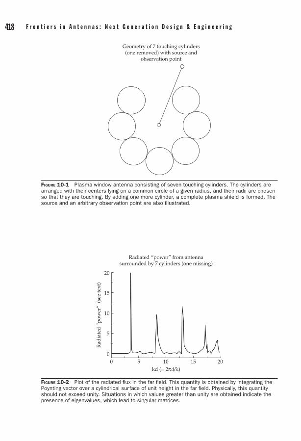
418 F r o n t i e r s i n A n t e n n a s : N e x t G e n e r a t i o n D e s i g n & E n g i n e e r i n g C h a p t e r 1 0 : P l a s m a A n t e n n a s 419
Figure 10-1 Plasma window antenna consisting of seven touching cylinders. The cylinders are arranged with their centers lying on a common circle of a given radius, and their radii are chosen so that they are touching. By adding one more cylinder, a complete plasma shield is formed. The source and an arbitrary observation point are also illustrated.
Geometry of 7 touching cylinders(one removed) with source and
observation point
Figure 10-2 Plot of the radiated flux in the far field. This quantity is obtained by integrating the Poynting vector over a cylindrical surface of unit height in the far field. Physically, this quantity should not exceed unity. Situations in which values greater than unity are obtained indicate the presence of eigenvalues, which lead to singular matrices.
20
Radiated “power” from antennasurrounded by 7 cylinders (one missing)
15
10
5
00 5 10 15 20
kd (= 2πd/λ)
Rad
iate
d “
pow
er”
(see
text
)

418 F r o n t i e r s i n A n t e n n a s : N e x t G e n e r a t i o n D e s i g n & E n g i n e e r i n g C h a p t e r 1 0 : P l a s m a A n t e n n a s 419
Figure 10-3 Far-field radiation patterns for various solutions illustrated in Fig. 10-2
150
120
90
60
30
0
330
300
270
240
210
180
1.0
Far-field radiation pattern for7 cylinders (one removed)
Nor
mal
ized
Inte
nsit
y0.8
0.6
0.4
0.2
0.0
0.2
0.4
0.6
0.8
1.0
kd = 5.2kd = 7.2kd = 12.2kd = 18.0
Figure 10-4 Plasma window consisting of 15 touching cylinders
Geometry of 15 touching cylinders(one removed) with source and
observation point

420 F r o n t i e r s i n A n t e n n a s : N e x t G e n e r a t i o n D e s i g n & E n g i n e e r i n g C h a p t e r 1 0 : P l a s m a A n t e n n a s 421
Figure 10-5 Plot of the far-field flux radiated from the 15-cylinder plasma window antenna. As in Fig. 10-2, this plot includes all solutions including nonphysical solutions for which the flux exceeds unity.`
20
15
10
5
0
0 5 10
kd (2πd/λ)
Rad
iate
d “
pow
er”
(see
text
)
Radiated “power” from antennasurrounded by 15 cylinders (one missing)
15 20
Figure 10-6 Far-field radiation patters for the 15-cylinder plasma antenna for several of the solutions illustrated in Fig. 10-5
150
120
90
60
30
0
330
300
270
240
210
180
1.0
Far-field radiation pattern for15 cylinders (one removed)
Nor
mal
ized
Inte
nsit
y
0.8
0.6
0.4
0.2
0.0
0.2
0.4
0.6
0.8
1.0
kd = 7.5kd = 11kd = 17.7

420 F r o n t i e r s i n A n t e n n a s : N e x t G e n e r a t i o n D e s i g n & E n g i n e e r i n g C h a p t e r 1 0 : P l a s m a A n t e n n a s 421
Figure 10-7 Beam half-width versus wavelength for the two plasma window antenna configurations. This is defined as the angle at which the far-field radiation pattern is reduced by a factor of one half.
Half beam width vs. wavelength(angle at half maximum)
40
35
30
25
20
15
10
5
00 5 10 15 20
kd (= 2πd/λ)
Hal
f Bea
m w
idth
(deg
rees
)
7 Cylinder plasma window15 Cylinder plasma window
10.4 Smart Plasma Antenna PrototypeDevelopment of the smart plasma antenna with reconfigurable radomes are given in papers by T. Anderson et al. [22], [23]. A smart plasma antenna has been developed. [24]. Various applications of the smart plasma antenna appear in patents by T. Ander-son [14]–[19].
The smart plasma antenna currently weighs about 15 pounds. It can steer the an-tenna beam 360° in milliseconds. The future prototypes could steer in microseconds using Fabry-Perot-Etalon effects. It is an intelligent, high performance steerable an-tenna with compact size, light weight, and it is stealth and jam resistant.
Figure 10-8 is a photograph of the smart plasma antenna commercial prototype.
10.5 Plasma Frequency Selective Surfaces
10.5.1 IntroductionPlasma FSS [8] use plasma as a substitute for metal in a FSS. FSSs have been used for filtering electromagnetic waves. Each FSS layer has to be modeled using numerical methods, and the layers are stacked in such a way as to create the desired filtering. Genetic algorithms are used to determine the stacking needed for the desired filtering;
422 F r o n t i e r s i n A n t e n n a s : N e x t G e n e r a t i o n D e s i g n & E n g i n e e r i n g C h a p t e r 1 0 : P l a s m a A n t e n n a s 423
this is a complicated and numerically expensive process. A method is developed to replace metal in a FSS with plasma elements. The plasma FSSs can be tuned to a de-sired filtering by varying the density in the plasma elements, which can save much of the routine analysis involved in the standard analysis of conventional FSS structures. The user simply tunes the plasma to get the filtering desired. Plasma elements offer the possibility of improved shielding along with reconfigurability and stealth. Plasma FSS can be made transparent by turning the plasma off. These characteristics all extend many of the previous scientific achievements in the development of the plasma an-tenna.
As the density of the plasma is increased, the plasma skin depth becomes smaller and smaller until the elements behave as metallic elements and we create filtering sim-ilar to FSS with metallic elements. Until the development of the metallic mode for the plasma, our theory and experiments showed that the plasma FSS had a continuous change in filtering. A basic mathematical model for a plasma FSS was developed by modeling the plasma elements as half-wavelength and full-wavelength dipole ele-ments in a periodic array on a dielectric substrate. The theoretical model with numeri-cal predictions predicted results in good agreement with our experiments on the plas-ma FSS. Theoretically Flouqet’s Theorem is used to connect the elements. The transmission and reflection characteristics of the plasma FSS as a function of plasma
Figure 10-8 Ruggedized smart plasma antenna prototype

422 F r o n t i e r s i n A n t e n n a s : N e x t G e n e r a t i o n D e s i g n & E n g i n e e r i n g C h a p t e r 1 0 : P l a s m a A n t e n n a s 423
density is developed. Frequencies from around 900 MHz to 12 GHz are utilized with a plasma density around 2 GHz. The plasma tubes are used to continuously vary the plasma density and can be observed the tunability of the reflection and transmission of electromagnetic waves. As the plasma density decays, the amount of transmitted elec-tromagnetic energy increases as expected. However, at electromagnetic signals, at fre-quencies well above the plasma frequency, the plasma FSS was transparent. The polar-ization of the transmitting antenna was rotated by 90° and produced a similar but reduced effect.
Next, an array of plasma FSSs was modeled. Similarly, we made the plasma FSS in the laboratory. Our theory and experiment were in close agreement. The plasma FSS is unique and new to the field of electromagnetic filtering. The potential payoff for this technology is high and the risk is moderate. It is moderate since we have developed plasma antennas with transmitters, but the plasma FSS is in some ways easier to de-velop since it does not require transmitters.
The plasma FSS can shield antennas, military electronics, and radar systems in a tunable way. If no shielding is needed, turning the plasmas off causes the shield to be invisible. Plasma FSS allows users to filter out any undesirable radiation, but at the same time enables operations outside that band. The potential for technology transfer is significant since the plasma FSS can be tuned to filter out unwanted radiation from commercial products or tuned to filter electromagnetic emissions to meet FCC EMC requirements.
10.5.2 Theoretical Calculations and Numerical ResultsAn FSS dipole array consists of a periodic array of vertically aligned scattering ele-ments. In traditional FSS structures, the scattering elements would be made of some material possessing good electrical conductivity (and thus high reflectivity).
For a plasma FSS structure, we imagine a scattering element to consist of gaseous plasma contained in a tube. The purpose of the present investigation is to determine the electromagnetic scattering properties of the array as a function of the reflectivity of the plasma elements.
10.5.2.1 method of CalculationThe response (reflection and transmission) of the plasma FSS is calculated in two stag-es: (1) the response for a perfectly conducting structure is given, (2) and reflectivity is then scale by a function that depends on the incident frequency and the plasma fre-quency so as to account for the scattering properties of the plasma. Details of these two steps will now be presented.
10.5.2.1.1 Periodic moment method In the first stage of calculation, we use the Peri-odic Moment Method as described in the book by Munk [25]. The elements are ap-proximated as thin flat wires. The scattered electric field produced by an incident plane wave of a single frequency is given by
E R IZ
D De
rnA
x y
j R r
ynk
( ) [( ˆˆ
= -- •
=-∞
∞
=-∞
∞
⊥ ±
±
∑∑2
β))( ) ( ˆ )( )].|| ||⊥ ±+P n P (10-37)
The quantities in this equation are defined as follows. The quantity IA is the current induced in a single element by the incident plane wave (see Munk [25]), Z is the impedance

424 F r o n t i e r s i n A n t e n n a s : N e x t G e n e r a t i o n D e s i g n & E n g i n e e r i n g C h a p t e r 1 0 : P l a s m a A n t e n n a s 425
of the medium which we take to be free space (Z = 377 W), R is the position vector of the observation point, and the scattering vector is defined by
ˆ ˆ ˆ ˆr xr yr zrx y z± = ± + , (10-38)
with
r s kDx x
x
= + λ, r s n
Dz zz
= + λ (10-39)
and
r s kD
s nDy x
xz
z
= - +
- +
12 2
λ λ. (10-40)
In these equations, Sx and Sz are the components of the unit vector specifying direc-tion of the incident plane wave. The array is assumed to lie in the xz-plane with repeat distances Dx and Dz, and the directions ± y indicate the forward and back scattering directions, respectively. Note that for sufficiently high values of the integers, n and k, the scattering vector component ry becomes imaginary corresponding to evanescent modes.
The remaining quantities (in the square brackets of the expression for the scattered field) are related to the way in which the incident electric field generates a voltage in an array element as is described in detail in Munk [25], The voltage induced in a scattering element by the incident field is given by
V R E R pP( ) ( ) ˆ= • (10-41)
where E R( ) is the electric field vector of the incident plane wave, p is a unit vector describing the orientation of the scattering element, and P is the pattern function for the scattering element. This is defined by
PI R
I l e dlt
t j lp s= - •∫1( )
( ) ˆ ˆβ
Element
(10-42)
where It(l) is the current distribution on the element located at R, I Rt ( ) is the current at the terminals of the scattering element (e.g., at the center of a dipole antenna), s is the unit vector denoting the plane wave incident direction, and b = 2p/l is the wave number. The unit vectors ⊥ n and ||n, which describe the electric field polarization, are defined by
⊥ =- +
+ˆ
ˆ ˆn
xr zr
r rz x
x z2 2
(10-43)
and
||ˆ ˆ ˆ ˆ ˆ ˆn n r
r rxr r y r r zr
x z
x y x z= × =+
- + +( ) -⊥1
2 22 2
yy zr
. (10-44)
The quantities ⊥ P, and || ,P are given by multiplying the pattern function by the appropriate direction cosine: ⊥ ⊥= •P p nPˆ ˆ , and || ||
ˆ ˆ .P p nP= • The effective terminal

424 F r o n t i e r s i n A n t e n n a s : N e x t G e n e r a t i o n D e s i g n & E n g i n e e r i n g C h a p t e r 1 0 : P l a s m a A n t e n n a s 425
current IA, which enters the equation for the scattered electric field, is obtained from the induced voltage and the impedance as
IV
Z ZAA L
=+
(10-45)
where ZL is the self-impedance of the scattering element, and ZA is the impedance of the array.
As in all moment methods, some approximation must be made regarding the de-tailed current distribution on the scattering elements. In order to calculate the pattern function, we assume the current distribution to be a superposition of current modes. The lowest order mode is taken to be a sinusoidal distribution of the form
I z z l0( ) cos( / ),= π (10-46)
assuming the scattering element to be a conductor of length l centered at the origin. Thus the lowest order mode corresponds to an oscillating current distribution of wave-length l = 2l. This lowest order mode gives rise to a radiation pattern equivalent to a dipole antenna with a current source at the center of the dipole. In effect, this mode divides the scattering elements into two segments. The next two higher order modes are constructed by dividing each half of the scattering element into two more seg-ments. These modes are written as
I z z l l1 2 2 4, ( ) cos[ ( / )/ ].= π m (10-47)
Physically these modes correspond to current distributions of wavelength l = l centered at ± l/4. The solution of the problem is then obtained by solving a matrix prob-lem to determine the coefficients of the various modes in the expansion of the currents. For the frequencies considered in this study only the lowest order mode was required, making the calculations extremely fast.
10.5.3 Scattering from a Partially-Conducting CylinderIn order to calculate the reflection from an array of plasma elements we make the phys-ically reasonable assumption that (to first order) the induced current distribution in a partially-conducting plasma differs from that of a perfectly-conducting scattering ele-ment only to the extent that the amplitude is different. In the limit of high conductivity the current distribution is the same as for a perfect conductor, and in the limit of zero conductivity the current amplitude is zero.
The scattered electric field is directly proportional to the induced current on the scattering element. In turn, the reflectivity is thus directly proportional to the square of the induced current in the scattering element. Thus, to find the reflectivity of the plas-ma array, we determine the functional dependence of the induced squared current vs. the electromagnetic properties of the plasma and scale the reflectivity obtained for the perfectly conducting case accordingly.
In order to obtain the scaling function for the squared current, consider the following model problem. The problem of scattering is solved from an infinitely extended dielectric cylinder possessing the same dielectric properties as a partially-ionized, collisionless plasma. Assume that the dielectric function for the plasma takes the following form
ε ωνν
( ) = -12
2p (10-48)

426 F r o n t i e r s i n A n t e n n a s : N e x t G e n e r a t i o n D e s i g n & E n g i n e e r i n g C h a p t e r 1 0 : P l a s m a A n t e n n a s 427
where n is the frequency of the incident electromagnetic wave, and np is the plasma frequency defined by
νπ
πp
n em
= 12
4 2 (10-49)
where n is the density of ionized electrons, and e and m, are the electron charge and mass, respectively. A good conductor is characterized by the limit of large plasma fre-quency in comparison to the incident frequency. At in the limit, in which the plasma frequency vanishes, the plasma elements become completely transparent.
Now, turn to the solution of the problem of scattering from a partially-conducting cylinder. The conductivity, and thus the scattering properties of the cylinder are speci-fied by the single parameter np. Solve the wave equation for the electric field
∇ = ∂∂
22
2
2
1E
cDt
, (10-50)
subject to the boundary conditions that the tangential electric and magnetic fields must be continuous at the cylinder boundary. Consider the scattering resulting from the in-teraction of the cylinder with an incident plane wave of a single frequency. Therefore, assuming all fields to have the harmonic time dependence
e-iwt (10-51)
where w = 2pn is the angular frequency. We are adopting the physics convention for the time dependence. Individuals more familiar with the electrical engineering convention can easily convert all subsequent equations to that convention by making the substitu-tion i → -j.
Next, we assume the standard approximation relating the displacement field to the electric field via the dielectric function:
D E( ) ( ) ( ).ω ε ω ω= (10-52)
By imposing cylindrical symmetry, the wave equation takes the form of Bessel’s equation
∂∂
+ ∂∂
+ ∂∂
+ =2
2 2
2
221 1
0E E E
k Eρ ρ ρ ρ ϕ
ε (10-53)
where k = w/c and (r,j) are cylindrical polar coordinates. The general solution of this equation consists of linear combinations of products of Bessel functions with complex exponentials. The total field outside the cylinder consists of the incident plane wave plus a scattered field of the form
E e A H k eikm
mmout
im= +=-∞
∞
∑ρ ϕ ϕρcos ( ) (10-54)
where Am is a coefficient to be determined, and Hm (kr) = Jm (kr) + iYm (kr) is the Hankel function that corresponds to outgoing cylindrical scattered waves. The field inside the cylinder contains only Bessel functions of the first kind since it is required to be finite at the origin:
E B J k emm
minim=
=-∞
∞
∑ ( ) .ρ ε ϕ (10-55)

426 F r o n t i e r s i n A n t e n n a s : N e x t G e n e r a t i o n D e s i g n & E n g i n e e r i n g C h a p t e r 1 0 : P l a s m a A n t e n n a s 427
To facilitate the determination of the expansion coefficients Am and Bm the incident plane wave is an expansion in Bessel6 functions:
e i J kik m
mm
ρ ϕ ρcos ( ).==-∞
∞
∑ (10-56)
To enforce continuity of the electric field at the boundary of the cylinder
E a E ain out( , ) ( , )ρ ϕ ρ ϕ= = = (10-57)
where the cylinder is assumed to have radius a. The next boundary condition is ob-tained by imposing continuity of the magnetic field. From one of Maxwell’s equations (Faraday’s law) we obtain
H i k E= - ∇ ×( / ) .1 (10-58)
The electric field is assumed aligned with the cylinder axis (TM polarization). This is the only case of interest since the scattering of the TE wave is minimal. Therefore, the tangential component of the magnetic field is
H i kEz
ϕ ρ= - -
∂∂
( / ) .1 (10-59)
By imposing the continuity of this field along with the continuity of the electric field, the following set of equations that determine the expansion coefficients is ob-tained:
i J ka A H ka B kamm m m m( ) ( ) ( )+ = ε (10-60)
and
i J ka A H ka B J kamm m m m m′ + ′ = ′( ) ( ) ( ) ,ε ε (10-61)
where the primes on the Bessel and Hankel functions imply differentiation with re-spect to the argument.
These equations are easily solved for the expansion coefficients as follows:
Ai J ka J ka J ka J ka
Hm
mm m m m
m
=- ′ - ′( ( ) ( ) ( ) ( ))
( (
ε ε εε kka J ka H ka J kam m m) ( ) ( ) ( ))′ - ′ε ε
(10-62)
and
Bi J ka H ka J ka H ka
H ka Jm
mm m m m
m m
=′ - ′
′
( ( ) ( ) ( ) ( ))
( ) (( ) ( ) ( ).
ka H ka J kam mε ε ε- ′ (10-63)
Inspection of these coefficients shows that in the limit e → 1, (i.e., zero plasma fre-quency) we obtain Am → 0, and Bm → im. Thus, in this limit, the scattered field vanishes and the field inside the cylinder simply becomes the incident field as expected.
The opposite limit of a perfectly conducting cylinder is also established fairly eas-ily but requires somewhat more care. Consider first the field inside the cylinder, which must vanish in the perfectly conducting limit. A typical term in the expansion of the electric field inside the cylinder is of the form
B J km m( ).ρ ε (10-64)

428 F r o n t i e r s i n A n t e n n a s : N e x t G e n e r a t i o n D e s i g n & E n g i n e e r i n g C h a p t e r 1 0 : P l a s m a A n t e n n a s 429
The perfect conductivity limit corresponds to taking the limit np → ∞ at fixed n. In this limit e → -np
2/n 2, and thus ε → i np /n . For large imaginary argument, the Bessel functions diverge exponentially. Therefore
B J k Om mp
( ) .ρ ε νν
→
→ 0 (10-65)
Lastly, we must establish that the tangential electric field just outside the cylinder vanishes in the perfect conductivity limit as expected. Using the fact that the Bessel functions diverge exponentially for large imaginary argument gives the following limit for the scattered wave expansion coefficient:
Ai J kaH kam
mm
m
→- ( )
( ). (10-66)
Thus, a typical term in the expansion for the scattered wave, evaluated just outside the cylinder, has the following limit:
A H ka i J kam mm
m( ) ( )→ - (10-67)
which exactly cancels the corresponding term in the expansion of the incident plane wave.
The scaling function defined below is used for the analysis of the scattering from a partially conducting cylinder to obtain a reasonable approximation to the scattering from a partially-conducting plasma FSS array based on the computed results for a perfectly-conducting array.
Proceed based on the following observations/assumptions.
1. The reflectivity of the plasma FSS array is determined entirely in terms of the scattered field in contrast to the transmitted field, which depends on both the incident and scattered fields.
2. The shape of the current modes on the partially conducting (plasma) FSS array is the same as for the perfectly-conducting array.
3. The only difference between the partially-conducting and perfectly-conducting arrays is the amplitude of the current modes.
It is now possible to conclude that the reflectivity of the plasma FSS can be deter-mined from that of the perfectly-conducting array by scaling the reflectivity of the perfectly-conducting array by some appropriately chosen scaling function. This con-clusion follows from the fact that the reflectivity is directly proportional to the squared amplitude of the current distribution on the scattering elements.
The scaling function (shown in Fig. 10-9) is made with the following approxima-tion. Assume that the amplitude of the current on a finite scattering segment in an FSS array scales with the plasma frequency in the same way as that for the isolated, infinitely-long cylinder.
The scaling function is defined as
S Ep( , ) .ν ν = -1 0 2out (10-68)

428 F r o n t i e r s i n A n t e n n a s : N e x t G e n e r a t i o n D e s i g n & E n g i n e e r i n g C h a p t e r 1 0 : P l a s m a A n t e n n a s 429
where Eout is the total tangential electric field evaluated just outside of the cylinder. Clearly, from the results of the previous section, the scaling function takes on the values
0 0 1 0. ( , ) .≤ ≤S pν ν (10-69)
for fixed incident frequency n, as the plasma frequency takes on the values
0 0. ≤ ≤ ∞νp . (10-70)
This function is plotted vs. np, for several values of the incident frequency.
10.5.3.1 ResultsTwo cases are presented: (1) an array designed to have a well-defined reflection reso-nance near 1 GHz (a bandstop filter), and (2) an array designed to operate as a good reflector for similar frequencies.
10.5.3.1.1 Switchable bandstop filter Each scattering element is assumed to be 15 cm in length, 1 cm in diameter. The vertical separation is taken to be 18 cm, while the lateral separation is taken to be 10 cm. The results for the perfectly-conducting case along with those for several values of the plasma frequency are presented in Fig. 10-10. A well-defined reflectivity resonance exists at 1 GHz. This result indicates that appreciable reflection occurs only for plasma frequencies above 2.5 GHz. The results of Fig. 10-10 illustrate the essence of the plasma FSS: a highly reflective bandstop filter can be achieved, which can be switched on and off simply by controlling the properties of the plasma.
Figure 10-9 Scaling function vs. plasma frequency for several values of the incident frequency. This function was obtained from the solution of the problem of scattering from a partially conducting, infinitely-long cylinder as discussed in the text.
Scaling Function vs. Plasma Frequency
Plasma Frequency (GHz)0
0.0
0.2
0.4
0.6
0.8
1.0
Incident: 0.1 GHzIncident: 0.5 GHzIncident: 1.5 GHzIncident: 2.5 GHz
5 10 15 20
Scal
ing
Func
tion
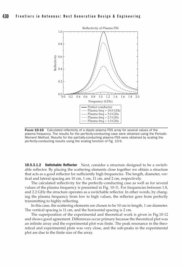
430 F r o n t i e r s i n A n t e n n a s : N e x t G e n e r a t i o n D e s i g n & E n g i n e e r i n g C h a p t e r 1 0 : P l a s m a A n t e n n a s 431
10.5.3.1.2 Switchable Reflector Next, consider a structure designed to be a switch-able reflector. By placing the scattering elements close together we obtain a structure that acts as a good reflector for sufficiently high frequencies. The length, diameter, ver-tical and lateral spacing are 10 cm, 1 cm, 11 cm, and 2 cm, respectively.
The calculated reflectivity for the perfectly-conducting case as well as for several values of the plasma frequency is presented in Fig. 10-11. For frequencies between 1.8, and 2.2 GHz the structure operates as a switchable reflector. In other words, by chang-ing the plasma frequency from low to high values, the reflector goes from perfectly transmitting to highly reflecting.
In this case, the scattering elements are chosen to be 10 cm in length, 1 cm diameter. The vertical spacing is 11 cm, and the horizontal spacing is 2 cm.
The superposition of the experimental and theoretical work is given in Fig.10-12 and shows good agreement. Differences occur primary because the theoretical plot was an infinite array and the experimental plot was finite. The peak resonance in the theo-retical and experimental plots was very close, and the sub-peaks in the experimental plot are due to the finite size of the array.
Figure 10-10 Calculated reflectivity of a dipole plasma FSS array for several values of the plasma frequency. The results for the perfectly-conducting case were obtained using the Periodic Moment Method. Results for the partially-conducting plasma FSS were obtained by scaling the perfectly-conducting results using the scaling function of Fig. 10-9.
1.0
0.8
0.6
0.4
0.2
0.00.0 0.2 0.4 0.6 0.8 1.0 1.2 1.4 1.6 1.8 2.0
Frequency (GHz)
Reflectivity of Plasma FSS
Ref
lect
ivit
y
Perfect conductorPlasma freq = 10.0 GHzPlasma freq = 5.0 GHzPlasma freq = 2.5 GHzPlasma freq = 1.0 GHz

430 F r o n t i e r s i n A n t e n n a s : N e x t G e n e r a t i o n D e s i g n & E n g i n e e r i n g C h a p t e r 1 0 : P l a s m a A n t e n n a s 431
Reflectivity of Plasma FSS Window
Ref
lect
ivit
y
1.0
0.8
0.7
0.5
0.3
0.2
0.00.0 0.2 0.4 0.6 0.8 1.0 1.2 1.4 1.6 1.8 2.0 2.2
Frequency (GHz)
Perfect conductorPlasma freq = 10.0 GHzPlasma freq = 5.0 GHzPlasma freq = 2.5 GHzPlasma freq = 1.0 GHz
Figure 10-11 Reflectivity for switchable plasma reflector. For frequencies between 1.8 and 2.2 GHz the structure operates as a good reflector for sufficiently high values of the plasma frequency.
Figure 10-12 Theoretical and experimental plots superimposed
Attenuation vs. Frequency
Att
enua
tion
(dB
)
22.0
20.0
18.0
16.0
14.0
12.0
10.0
8.0
6.0
4.0
2.0
0.04.54.03.53.02.52.01.51.00.5
Frequency in GHz
Theory (infinite array)Experiment (finite array)
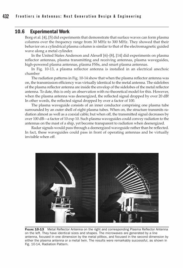
432 F r o n t i e r s i n A n t e n n a s : N e x t G e n e r a t i o n D e s i g n & E n g i n e e r i n g C h a p t e r 1 0 : P l a s m a A n t e n n a s 433
10.6 Experimental WorkBorg et al. [4], [5] did experiments that demonstrate that surface waves can form plasma columns over the frequency range from 30 MHz to 300 MHz. They showed that their behavior on a cylindrical plasma column is similar to that of the electromagnetic guided wave along a metal cylinder.
In the United States Anderson and Alexeff [6]–[8], [14] did experiments on plasma reflector antennas, plasma transmitting and receiving antennas, plasma waveguides, high-powered plasma antennas, plasma FSSs, and smart plasma antennas.
In Fig. 10-13, a plasma reflector antenna is installed in an electrical anechoic chamber
The radiation patterns in Fig. 10-14 show that when the plasma reflector antenna was on, the transmission efficiency was virtually identical to the metal antenna. The sidelobes of the plasma reflector antenna are inside the envelop of the sidelobes of the metal reflector antenna. To date, this is only an observation with no theoretical model for this. However, when the plasma antenna was deenergized, the reflected signal dropped by over 20 dB! In other words, the reflected signal dropped by over a factor of 100.
The plasma waveguide consists of an inner conductor comprising one plasma tube surrounded by an outer shell of eight plasma tubes. When on, the structure transmits ra-diation almost as well as a coaxial cable; but when off, the transmitted signal decreases by over 100 dB—a factor of 10 exp 10. Such plasma waveguides could convey radiation to the antennas on the mast of a ship, yet become transparent to radiation when deenergized.
Radar signals would pass through a deenergized waveguide rather than be reflected. In fact, these waveguides could pass in front of operating antennas and be virtually invisible when off.
Figure 10-13 Metal Reflector Antenna on the right and corresponding Plasma Reflector Antenna on the left. They have identical sizes and shapes. The microwaves are generated by a line antenna, focused in one dimension by the metal pillbox, and focused in the second dimension by either the plasma antenna or a metal twin. The results were remarkably successful, as shown in Fig. 10-14, Radiation Pattern.
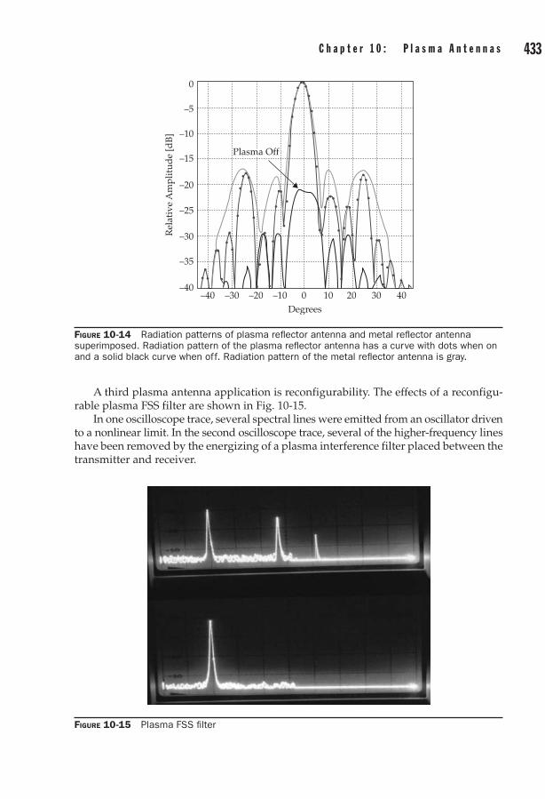
432 F r o n t i e r s i n A n t e n n a s : N e x t G e n e r a t i o n D e s i g n & E n g i n e e r i n g C h a p t e r 1 0 : P l a s m a A n t e n n a s 433
A third plasma antenna application is reconfigurability. The effects of a reconfigu-rable plasma FSS filter are shown in Fig. 10-15.
In one oscilloscope trace, several spectral lines were emitted from an oscillator driven to a nonlinear limit. In the second oscilloscope trace, several of the higher-frequency lines have been removed by the energizing of a plasma interference filter placed between the transmitter and receiver.
Figure 10-14 Radiation patterns of plasma reflector antenna and metal reflector antenna superimposed. Radiation pattern of the plasma reflector antenna has a curve with dots when on and a solid black curve when off. Radiation pattern of the metal reflector antenna is gray.
0
–5
–10
–15
–20
–25
–30
–35
–40–40 –30 –20 –10 0 10 20 30 40
Degrees
Rel
ativ
e A
mpl
itud
e [d
B]
Plasma Off
Figure 10-15 Plasma FSS filter
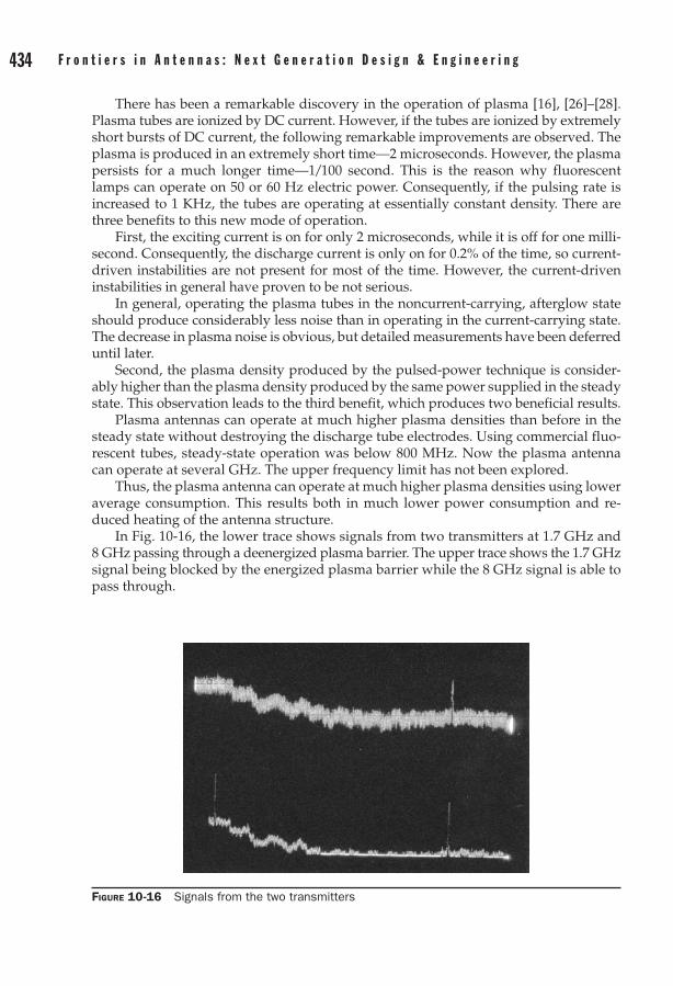
434 F r o n t i e r s i n A n t e n n a s : N e x t G e n e r a t i o n D e s i g n & E n g i n e e r i n g C h a p t e r 1 0 : P l a s m a A n t e n n a s 435
There has been a remarkable discovery in the operation of plasma [16], [26]–[28]. Plasma tubes are ionized by DC current. However, if the tubes are ionized by extremely short bursts of DC current, the following remarkable improvements are observed. The plasma is produced in an extremely short time—2 microseconds. However, the plasma persists for a much longer time—1/100 second. This is the reason why fluorescent lamps can operate on 50 or 60 Hz electric power. Consequently, if the pulsing rate is increased to 1 KHz, the tubes are operating at essentially constant density. There are three benefits to this new mode of operation.
First, the exciting current is on for only 2 microseconds, while it is off for one milli-second. Consequently, the discharge current is only on for 0.2% of the time, so current-driven instabilities are not present for most of the time. However, the current-driven instabilities in general have proven to be not serious.
In general, operating the plasma tubes in the noncurrent-carrying, afterglow state should produce considerably less noise than in operating in the current-carrying state. The decrease in plasma noise is obvious, but detailed measurements have been deferred until later.
Second, the plasma density produced by the pulsed-power technique is consider-ably higher than the plasma density produced by the same power supplied in the steady state. This observation leads to the third benefit, which produces two beneficial results.
Plasma antennas can operate at much higher plasma densities than before in the steady state without destroying the discharge tube electrodes. Using commercial fluo-rescent tubes, steady-state operation was below 800 MHz. Now the plasma antenna can operate at several GHz. The upper frequency limit has not been explored.
Thus, the plasma antenna can operate at much higher plasma densities using lower average consumption. This results both in much lower power consumption and re-duced heating of the antenna structure.
In Fig. 10-16, the lower trace shows signals from two transmitters at 1.7 GHz and 8 GHz passing through a deenergized plasma barrier. The upper trace shows the 1.7 GHz signal being blocked by the energized plasma barrier while the 8 GHz signal is able to pass through.
Figure 10-16 Signals from the two transmitters
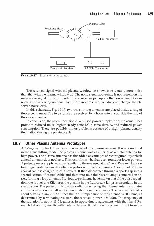
434 F r o n t i e r s i n A n t e n n a s : N e x t G e n e r a t i o n D e s i g n & E n g i n e e r i n g C h a p t e r 1 0 : P l a s m a A n t e n n a s 435
The received signal with the plasma window on shows considerably more noise than that with the plasma window off. The noise signal apparently is not present on the microwave signal, but is primarily due to receiver pickup via the power line. Discon-necting the receiving antenna from the panoramic receiver does not change the ob-served noise level.
In this schematic, Fig. 10-17, two transmitting antennas are placed inside a ring of fluorescent lamps. The two signals are received by a horn antenna outside the ring of fluorescent lamps.
In conclusion, the recent inclusion of a pulsed power supply for our plasma tubes provides reduced noise, higher steady-state DC plasma density, and reduced power consumption. There are possibly minor problems because of a slight plasma density fluctuation during the pulsing cycle.
10.7 Other Plasma Antenna PrototypesA 2 Megawatt pulsed power supply was tested on a plasma antenna. It was found that in the transmitting mode, the plasma antenna was as efficient as a metal antenna for high power. The plasma antenna has the added advantages of reconfigurability, which a metal antenna does not have. This reconfirms what has been found for lower powers. A pulsed power supply was used similar to the one used at the Naval Research Labora-tory to generate megawatt radiation pulses with metal antennas. A section of 50 Ohm coaxial cable is charged to 25 Kilovolts. It then discharges through a spark gap into a second section of coaxial cable and then into four fluorescent lamps connected in se-ries, forming a loop antenna. Previous experiments have shown that if the pulse repeti-tion rate is over one Kilohertz, the plasma in the fluorescent lamps is essentially in the steady state. The pulse of microwave radiation entering the plasma antenna radiates and is received on a small wire antenna about one meter away. The received signal is about 5 Volts in amplitude. Since the input impedance of the antenna is 50 Ohms, as determined by terminating resistors, the received power is ½ Watt. The frequency of the radiation is about 13 Megahertz, in approximate agreement with the Naval Re-search Laboratory results with metal antennas. To calibrate the power output from the
Figure 10-17 Experimental apparatus
Panoramic Receiver 1.7 GHz Transmitter
Receiving Horn
8 GHz Transmitter
Plasma Tubes

436 F r o n t i e r s i n A n t e n n a s : N e x t G e n e r a t i o n D e s i g n & E n g i n e e r i n g C h a p t e r 1 0 : P l a s m a A n t e n n a s 437
transmitter, we replaced the plasma antenna with a wire-loop antenna of the same physical dimensions. We found that the received power from the pulsed power transmitter was the same as for the plasma antenna. The wire antenna was disconnected from the pulsed power supply, and connected it to a 10 Megahertz transmitter; the received power was measured on a panoramic receiver. The transmitter was then connected directly into the panoramic receiver which adjusted the signal strength to the previous value and recorded the attenuation needed to do so. The attenuation required was 70 decibels. If the power received from the pulsed power supply is multiplied via the plasma antenna by 70 decibels, the radiated power from the plasma antenna is 5 Megawatts! This result is in agreement with the measured radiation output from the Naval Research Laboratory where, a metal antenna was used.
Figure 10-18 is a photograph of AM/FM radio plasma antenna.
10.8 Plasma Antenna Thermal Noise This material is an expansion of the work in the book by Reif [29] for the standard Ny-quist’s Theorem in which the well-known result is H = 4 RKT, where H is the noise spectrum as Volts squared per Hertz (not Watts), R is the resistance of the object in Ohms (not Ohms per unit length), K is Boltzmann’s constant in Joules per degree K, and T is the temperature in degrees K.
The book acknowledges that the equation is a low-frequency approximation, but states that this approximation is correct, since in metals the collision frequency is a terahertz.
The correction term found by Anderson [30], [31] is
H
cc
=+
41
12 2
2
RKT( )πυ
υ
(10-71)
Figure 10-18 Plasma antenna for AM/FM radio prototype

436 F r o n t i e r s i n A n t e n n a s : N e x t G e n e r a t i o n D e s i g n & E n g i n e e r i n g C h a p t e r 1 0 : P l a s m a A n t e n n a s 437
where u is the frequency of the transmitter in Hertz, and uc is the electron-gas atom collision frequency in Hertz. The factor of 2p is a numerical constant that arises from the Fourier Transform Process.
To compare the noise in a given spectral region, R and uc for metals and for plasmas
must be obtained. Considering operation at 10 GHz (3 cm wavelength), in metals, uc from textbook Reif [29], is 1 THz.
For the resistance, assuming a rod 1 cm square in cross section and 3 cm long. The resistance of copper is 1.692exp-6 (“Handbook of Chemistry and Physics” [32]), so the metal antenna would be 5.076 exp-6 Ohm if skin depth were to be neglected.
Skin depth is given by
212
σµω
(10-72)
where s is the conductivity, m is the permittivity, and w is the angular frequency of the microwaves (radians per second or 2pu in Hertz).
The skin depth is 2 exp-5 cm. Hence, the resistivity corresponds to a copper sheet 3 cm long, 4 cm wide, and 2 exp-5 cm thick. This corresponds to a resistance of .063 Ohms.
The temperature of the copper is 300° Kelvin.For the plasma, the collision frequency is computed as follows. In Cobine’s book,
“Gaseous Conductors” [33], assume the pressure in a fluorescent tube to be a maxi-mum of 2 mm hg. The electron-gas atom scattering cross section corresponds to an electron temperature of 1 electron-volt, is deep in the Ramsauer minimum. The mean-free-path is about 1 cm at a pressure of 1 mm hg. This gives a scattering cross section of 2.8 exp-17 cm squared (it is at the Ramsauer minimum), at a pressure of 1 mm hg.
The electron velocity corresponds to 1 electron-volt. The thermal velocity is
vKTm
= , where v is the velocity, K is Boltzmann’s constant, T is the electron tempera-
ture, and m is the electron mass. Inserting the proper values gives an electron thermal velocity of 4.2 exp 7 cm per second. Using the atom density at mm hg to be 7.02 exp 16 per cc, the collision frequency is computed to be 82 MHz. Actually, if the tube is about 1 cm in diameter, the collision frequency at the wall exceeds this.
Concerning the resistance of the tube, Cobine [33] gives the voltage drop for a 9 inch tube to be 45 and for a 48 inch tube to be 108. Subtracting these to get rid of the cathode drop and to find the voltage drop on the positive column, we get 1.62 volts per inch, or 0.638 volts per cm. The current ranged from .15 to .42 Ampere. Since the tube has essentially a voltage drop independent of current, we use the .42 Ampere value. This yields a resistance of 1.52 Ohms per cm. For a 3 cm long column of plasma, we have 4.56 Ohms.
Computing the noise figure in volts squared per Hertz, the metal gives us 1.04 exp-21.For the plasma antenna at 10 GHz, we obtain 4.29 exp-24.Thus, in this frequency range, the noise in the plasma antenna is much less than the
metal antenna. Of course, at low enough frequencies, the inequality is reversed, but we can address that by reducing the gas pressure in custom made plasma tubes. Note that we used the upper limit for gas pressure in this report on the plasma tube. In the patent application, pressures two thousand times lower have been used. (U.S. Patent 1,790,153). Using the lowest pressure would reduce the plasma noise by about a factor of 2000.

438 F r o n t i e r s i n A n t e n n a s : N e x t G e n e r a t i o n D e s i g n & E n g i n e e r i n g C h a p t e r 1 0 : P l a s m a A n t e n n a s 439
Keep in mind that this analysis has been and is for a fluorescent lamp. Plasma an-tennas have been made out of fluorescent lamps because they are inexpensive; this shows that people can do research and development and build prototypes of the plas-ma antenna technology inexpensively.
When plasma antennas are ruggedized with custom-made plasma tubes, the gas pressure inside the plasma tubes can be much less than in a fluorescent bulb which lowers the frequency at which the plasma antenna thermal noise is equal to the metal antenna thermal noise.
Using the highest gas pressure in a fluorescent tube of 2 millimeters, the frequency at which the plasma antenna and the metal antenna have the same thermal noise is 1.27 GHz. Using the lowest gas pressure of a fluorescent tube of 1 micron, this crossover frequency at which the plasma antenna thermal noise and the metal antenna thermal noise are equal is much lower. Above the crossover frequency where the thermal noise of the plasma antenna and the metal antenna, the plasma antenna thermal noise drops rapidly.
As stated above, custom-made plasma tubes can be made such that pressure is much lower than in a fluorescent lamp. This would make the number at which the thermal noise of the plasma antenna and the metal antennas are equal much lower than 1.27 GHz antenna frequency.
Again, fluorescent tubes have often been used to make plasma antennas because this has been an inexpensive way to do our plasma antenna research and development. Custom-made plasma tubes are now being designed to be rugged and to have lower noise than metal antennas over very wide frequency range.
A patent has been filed on low thermal noise designs of plasma antennas [34].
10.9 Current Work Done to make Plasma Antennas RuggedThe plasma tubes have been housed in a strong and lightweight synthetic foam called SynFoamTM (see Fig. 10-19) made by Utility Development Corporation (http://www.udccorp .com/products/synfoamsyntacticfoam.html) [35] which can be molded into various shapes. SynFoam is a high performance syntactic foam combining high strength, heat resistant,
Figure 10-19 SynFoam housing for plasma tubes. Experiments are planned using the cavities in the SynFoam to directly house the plasma gas without using glass tubes at all.

438 F r o n t i e r s i n A n t e n n a s : N e x t G e n e r a t i o n D e s i g n & E n g i n e e r i n g C h a p t e r 1 0 : P l a s m a A n t e n n a s 439
light weight, and very low moisture absorption. SynFoam’s syntactic foam products feature a density of less than 20 pcf and a compressive strength greater than 2000 psi. The index of refraction of the SynFoam is nearly 1 so it is transparent to rf signals.
10.10 Latest Developments on Plasma AntennasPlasma tubes will intercept microwaves regardless of polarization. A layer of plasma tubes is used as a microwave reflector. The plasma tubes work extremely well in inter-cepting microwave radiation when the incident wave electric field is parallel to the tubes. However, if the electric field is perpendicular to the tubes, the normally induced plasma current cannot flow, and the plasma effects are not expected to appear. When the plasma tubes were experimentally tested with the electric field perpendicular to the tubes, the plasma tubes not only intercepted the microwave signal, but the ob-served cutoff with a pulsed plasma lasted almost twice as long.
10.10.1 Theory for Polarization EffectThe polarization effect appears to be due to an electrostatic resonance, and preliminary calculations suggest that a normally ignored term in Maxwell’s Equations is responsible.
∇2 E - ∇(∇ ⋅ E) = m0 e0 ωpE
t2
2
2+ ∂
∂
(10-73)
The term responsible appears to be:
∇(∇ · E). (10-74)
10.10.2 Generation of Dense Plasmas at Low Average Power Input by Power Pulsing
One of the remarkable plasma effects experimentally discovered is the large increase in plasma density at the same average power input provided by pulsing the power input [16], [18], [26]–[28]. In our experiments, a density increase of over 100 has been observed. Although various experimenters have observed similar effects using different power input techniques, to our knowledge no one has yet provided a theoretical explanation.
A theoretical model for this effect is provided. Since the power is obviously being deposited into the plasma, we assume that during the power input an enhanced plas-ma loss occurs. This plasma loss occurs on a time scale, T1. On turning off the power input, this plasma loss process disappears on a time scale, T2. The resulting afterglow plasma disappears on a much slower time scale, T3. Modeling this as a system driven by a power delta function repeating on a time period, T4, the height of the delta func-tion is proportional to, T4, so the longer the time between pulses, the higher the delta function; but the average power input is preserved.
As a first approximation on a single pulse basis, we obtain
NN
TT
TT
AG
SS
= -
exp 2
1
4
5
(10-75)
440 F r o n t i e r s i n A n t e n n a s : N e x t G e n e r a t i o n D e s i g n & E n g i n e e r i n g C h a p t e r 1 0 : P l a s m a A n t e n n a s 441
where NA G is the afterglow density during pulsing and Nss is the density during steady-state operation. In our experiments, T4 is about 1000 times T5 (the duration of the delta function). If we assume that the fast decay process, T1, is of the same approximate length as the time in which this decay process disappears, T2, the above calculation yields a density enhancement of about 300. This number agrees with our observed density enhancement. This calculation ignores plasma left over from the preceding pulse, but most of this is dumped by the effects of the pulse. In any case, it can only improve plasma density.
10.10.3 Fabry-Perot Resonator for Faster Operation of the Smart Plasma Antenna
The characteristic decay time of the plasma after power turn-off is typically many mil-liseconds, so the opening time of such a barrier generally is also predicted also to be many milliseconds. However, the plasma barrier can be opened and closed in faster time scales.
This can be done by increasing the plasma density rather than waiting for it to de-cay. If a standing wave is produced between the two lawyers of plasma that results in microwave transmission, this may be analogous to the transmission found in an optical Fabry-Perot Resonator. The secret lies in the boundary layer behavior of the plasma. Once microwave cutoff occurs, one would expect the plasma behavior to be static. What actually occurs is that at microwave cutoff, the reflection is in-phase with the incident wave, in analogy to an open coaxial line. (The electron and displacement cur-rents are equal, but out-of-phase.) As the plasma density further increases, the reflection smoothly changes from in-phase to 180° out-of-phase, in analogy to a shorted coaxial line. (The reflection current is much greater than the displacement current.) The bound-ary condition at a vacuum-plasma interface of the reflected electric field in terms of the incident electric field is
Eii
Er = -+
11 0
ββ (10-76)
where the phase shift is given by
βωω
= -p2
21 . (10-77)
The consequence of this phase shift is that, given any kind of a plasma resonator, if the plasma density is raised high enough, the resonance required for the Fabry-Perot effect to take place must occur.
ReferencesW. Manheimer, “Plasma reflectors for electronic beam steering in radar systems,” [1] IEEE Transactions on Plasma Science, vol. 19, no. 6, p. 1228, December 1993. J. Mathew, R. Meger, J. Gregor, R. Pechacek, R. Fernsler, W. Manheimer, and A. Robson, “Electronically [2] Steerable Plasma Mirror for Radar Applications,” IEEE International Radar Conference, p. 742, June 1995.M. Moisan, A. Shivarova, and A. W. Trivelpiece, [3] Physics of Plasmas 20, 1331, 1982.G. Borg, J. Harris, N. Martin, D. Thorncraft, R. Milliken, D. Miljak, B. Kwan, T. Ng, and J. Kircher, [4] “Plasmas as antennas: Theory, experiment, and applications,” Physics of Plasmas, vol. 7, no. 5, p. 2198, May 2000.

440 F r o n t i e r s i n A n t e n n a s : N e x t G e n e r a t i o n D e s i g n & E n g i n e e r i n g C h a p t e r 1 0 : P l a s m a A n t e n n a s 441
G. G. Borg, D. G. Miljak, J. H. Harris, and N. M. Martin, Appl. Phys. Lett. 74, 3272, 1999.[5] I. Alexeff, and T. Anderson, “Experimental and theoretical results with plasma antennas,” [6] IEEE Transactions on Plasma Science, vol. 34, no. 2, April 2006.I. Alexeff, and T. Anderson[7] , “ Recent results of plasma antennas,” Physics of Plasmas, 15, 057104 (2008).T. Anderson, and I. Alexeff, “Plasma frequency selective surfaces,” [8] IEEE Transactions on Plasma Science, vol. 35, no. 2, p. 407, April 2007.D. C. Jenn, “Plasma antennas: Survey of techniques and the current state of the Art,” Naval Postgraduate [9] School, September 29, 2003, http://faculty.nps.edu/jenn/pubs/PlasmaReportFinal.pdf N. Krall, and A. Trivelpiece, “Principals of plasma physics,” pp. 84–98, McGraw-Hill Inc, 1973. [10] F. Chen, [11] Introduction to Plasma Physics and Controlled Fusion, Vol. 1, pp. 53–78. 2nd ed., Plenum Press. 1984.http://www.pppl.gov/~hammett/courses/trieste01/aps95_invited.pdf[12] C. Balanis, [13] Antenna Theory, 2nd ed., p. 143. John Wiley & Sons. 1997.www.ionizedgasantennas.com, www.haleakala-research.com, and www.drtedanderson.com[14] T. Anderson, “Multiple tube plasma antenna,” U.S. Patent number 5,963,169. [15] T. Anderson, and I. Alexeff, “Reconfigurable scanner and RFID,” Application Serial Number [16] 11/879, 725.T. Anderson, “ Configurable arrays for steerable antennas and wireless network incorporating the [17] steerable antennas.” U.S. patent 7, 342, 549.T. Anderson, “Reconfigurable scanner and RFID system using the scanner. ” U.S. patent 6, 922, 173.[18] T. Anderson, “Configurable arrays for steerable antennas and wireless network incorporating the [19] steerable antennas,” U.S. patent 6,870,517.T. Anderson, and I. Alexeff, “Theory and experiments of plasma antenna radiation emitted through [20] plasma apertures or windows with suppressed back and side lobes,” International Conference on Plasma Science, 2002.T. Anderson, “Storage and release of electromagnetic waves by plasma antennas and waveguides,” [21] pp. 74–82, 33rd AIAA Plasmadynamics and Lasers Conference, 2002.T. Anderson, and I. Alexeff, “Plasma frequency selective surfaces,” [22] International Conference on Plasma Science, 2003.T. Anderson, and I. Alexeff, “Theory of plasma windowing antennas,” [23] IEEE ICOPS, Baltimore, June 2004.http://www.haleakala-research.com/uploads/OperatingPlasmaAntenna.pdf[24] B. A. Munk, [25] Frequency Selective Surfaces,” Wiley Interscience, 2000.I. Alexeff, “ Pulsed plasma element,” U.S. patent 7,274,333.[26] T. Anderson, “Tunable plasma frequency devices,”, U.S. patent, 7,292,191.[27] T. Anderson, “Tunable plasma frequency devices”, U.S. patent, 7,453,403.[28] F. Reif, Fundamentals of Statistical and Thermal Physics, pp. 585–589. McGraw-Hill, 1965.[29] T. Anderson, “Electromagnetic noise from frequency driven and transient plasmas,” [30] IEEE International Symposium on Electromagnetic Compatibility, Symposium Record, vol. 1, Minneapolis, MN, August 19–23, 2002.T. Anderson., “Control of electromagnetic interference from arc and electron beam welding by [31] controlling the physical parameters in arc or electron beam: Theoretical model,” IEEE Symposium Record, vol. 2, pages 695–698, 2002.CRC Handbook Chemistry and Physics[32] , 85th ed., CRC Press, 2004.J. D., Cobine, [33] Gaseous Conductors Theory and Engineering Applications. McGraw-Hill, 1941. T. Anderson, and I. Alexeff, “High SNR plasma antenna” Application Serial Number 12/324,876.[34] http:[35] //www.udccorp.com/products/synfoamsyntacticfoam.html.

This page intentionally left blank

Chapter 11Numerical Methods in
antenna Modeling
J.-F. Lee, r. Lee, V. rawat, K. Sertel, and F. L. teixeira
In this chapter, we present three main numerical methods that are capa ble of solving complex electromagnetic wave radiation and scattering problems in three-dimensional (3D). They are: time-domain methods including finite-difference and finite-element time-domain methods, finite-element frequency-domain methods, and a conformal domain decomposition method using interior penalty formulation. This chapter starts by discussing the state-of-art time-domain methods, followed by a detailed description of the frequency-domain finite-element methods (FEM). Finally, we include a conformal domain decomposition method which does not re quire additional auxiliary variables. Throughout the chapter, various complex and electrically large numerical examples are also included.
11.1 Time-Domain ModelingIn this section, we shall discuss some time-domain computational electro magnetics (CEM) methods for antenna analysis.1 Due to space limitations, we will focus on the finite-difference time-domain (FDTD) and finite-element time-domain (FETD) methods [8], [10], [1]. These are two of the most popular methods presently available and widely used in many commercially available software packages.
11.1.1 FDTD and FETD: Basic ConsiderationsTime-domain simulations of antenna problems are sometimes an attractive al ternative to frequency-domain simulations because they can produce wideband data with a single code execution. As a result, they are particularly suited, for example, to ultra-wideband antenna problems, as will be illustrated later on in this section. Antenna scenarios involving nonlinear and/or time-varying media/components are more easily tackled in the time-domain as well.
In general, a time-domain discretization strategy for Maxwell’s equations may involve either explicit or implicit “marching-on-time” updates (also called
1 Portions of this material have previously appeared in [1]–[7].
443

444 F r o n t i e r s i n a n t e n n a s : N e x t G e n e r a t i o n D e s i g n & e n g i n e e r i n g C h a p t e r 1 1 : N u m e r i c a l M e t h o d s i n a n t e n n a M o d e l i n g 445
“time-stepping”). Explict updates refer to time-domain discretizations whereby the fields to be determined at a given time step depend only on (known) field values at previous time steps. On the other hand, implicit updates refers to time-domain discretizations whereby present field values depend not only on previous field values but also on each other. As a result, implicit updates require the solution of a linear system (typically sparse) at every time step, whereas explicit update may not (the latter are denoted “matrix-free”). This is a clear advantage for explicit updates. The most celebrated explicit time-domain method is the conventional Yee’s FDTD scheme [8]. However, explicit updates are subject to the so-called Courant limit, which sets a bound on the maximum size of the time increment from numerical stability considerations [11]. In contrast, some implicit updates are not subject to the Courant limit and the time increment size in this case can be chosen from accuracy considerations only, which can lead to a time increment much larger than the one set by the Courant limit.
In its basic form as introduced by Yee and pioneered by Taflove, the FDTD method is conceptually very simple and relies on the approximation of time and space derivatives of Maxwell curl equations by central differences on staggered grids, leading to a scheme which is second-order accurate in both space and time [8]. The grid in FDTD is typically a structured rectangular grid. Because FDTD is matrix-free, its memory requirements scale only linearly with the num ber of unknowns. This, added to the fact that FDTD is massively parallelizable, makes FDTD quite suited for petascale computing and beyond. Higher-order versions of FDTD also exist, which trade simulation accuracy by sparsity.
Being naturally constructed for unstructured irregular grids, FETD is quite suited for numerical solution of antenna problems in complex geometries where the use of a rectangular FDTD grid would give rise to staircasing error. FETD is also suited for implementations with p- and h-refinement capabilities. However, FETD methods in irregular grids lead to implicit schemes requiring the solu tion of a sparse linear system at every time step. For Maxwell’s equations, it is possible to obtain explicit (“matrix-free”) FEM using, for instance, mass (matrix) lumping, but not without shortcomings (in particu lar, they are prone to numerical instabilities). There are two basic approaches for constructing FETD algorithms for Maxwell equations. The first approach is based on the discretization of the second-order vector Helmholtz wave equa tion (for either the electric or magnetic field) by expanding the unknown field in terms of local basis functions—most commonly (curl-conforming) Whitney edge elements—followed by application of the method of weighted residuals via an inner product with test functions [10]. In order to produce symmetric ma trices (assuming reciprocal media), the set of test functions is chosen identical to the set of basis functions (Galerkin testing). The second FETD approach is based on the discretization of the first-order Maxwell curl equations by expanding the electric and magnetic fields in terms of “mixed” elements, most commonly Whitney edge elements for the electric field and (div-conforming) Whitney face elements for the magnetic flux density [12]. This choice avoids the appearance of spurious modes (by satisfying a discrete version of the de Rham diagram). This is followed by either (a) application of the method of weighted residuals with appropriate (also mixed) test functions or (b) by the use of incidence matrices and construction of discrete Hodge operators [12].

444 F r o n t i e r s i n a n t e n n a s : N e x t G e n e r a t i o n D e s i g n & e n g i n e e r i n g C h a p t e r 1 1 : N u m e r i c a l M e t h o d s i n a n t e n n a M o d e l i n g 445
11.1.2 UWB Antenna Problems in Complex MediaSome of the antenna problems where FDTD and FETD are mostly suited for involve UWB operation, as noted above, and/or scenarios where the antenna is loaded by or in close proximity of inhomogeneous and possibly dispersive media. This, of course, necessitates algorithms able to incorporate frequency dispersive effects in the time-domain. In linear, time-invariant, isotropic media, the time-domain constitutive equation relating the electric field and the electric flux density D is typically cast as a convolution between E and the permittivity as follows
D r t r t E r dt
( , ) ( , ) ( , )= −−∞∫ τ τ τ (11-1)
( , ) ( ) ( , )r t t r te= +0 0δ χ (11-2)
where ( , ) [ ( , )]r t r= −F 1 ω is the time-domain permittivity function, F stands for Fourier transformation, 0 is the vacuum permittivity, d (t) is the Dirac delta function, and χe r t( , ) is the (time-domain) electric susceptibility function. In FDTD or FETD, the time variable is discretized as tl = lΔt with l = 0, 1, 2 . . . . We denote E(lΔt) = El, and similarly for the other fields. A direct implemen tation of the convolution above would require storage of the entire past time series of El, which is obviously impractical. However, due to the exponential nature of the susceptibility kernel, a recursive convolution can be implemented instead where storage of only a few previous time-step values is needed (the actual number depends on the order of accuracy sought—two or three steps are typical in FDTD). The terminology RC is usually reserved for the low-order im plementation that assumes a piecewise constant electric field between each time step. Other implementations for the convolution also exist, with the piecewise linear recursive convolution (PLRC) [2] being a popular choice and illustrated below. Since conventional FDTD is second-order accurate in time, it is usually not advantageous to implement a high order accurate recursive convolution un less the time integration in the core FDTD update (of Maxwell curl equations) itself is of high order.
In linear time-invariant media, the constitutive equation in dispersive media can also be cast as ordinary differential equation (ODE) in time involving D and E or, alternatively, involving E and some induced macroscopic polarization field. In linear time-invariant media, this ODE is linear with constant coefficients (in time) with the generic form
a rD r t
tb r
E r ttp
p
p p
p
pp
N
p
N
( )( , )
( )( , )∂
∂= ∂
∂==∑
00
211
∑ (11-3)
or an analogous ODE involving E and polarization fields. In some cases, addi tional dynamic fields are present in the physical model so that an ODE system ensues.
The order N1, N2 and the coefficients a r b rp p( ), ( ) above depend on the par ticular dispersion model considered for ( , )r ω . In FDTD, the above ODE can be discretized by, for example, recasting it as an equivalent system of ODEs involving only first- and/or second-order differential equations, followed by a FD approximation in time of each differential equation [2]. This is commonly referred to as the auxiliary differential equation (ADE) approach.
446 F r o n t i e r s i n a n t e n n a s : N e x t G e n e r a t i o n D e s i g n & e n g i n e e r i n g C h a p t e r 1 1 : N u m e r i c a l M e t h o d s i n a n t e n n a M o d e l i n g 447
The presence of inhomogeneous media of course poses no difficulties for FDTD or FETD as they are volumetric discretization schemes where medium properties are naturally described point-wise. Both methods are also able to model anisotropic media without much difficulty [1], [13], [14]. A recent survey of FDTD and FETD as applied to problems involving media having more complex properties (nonlinear, anisotropic, etc.) can be found in [1]
11.1.3 PML Absorbing Boundary ConditionFor problems in unbounded regions, which comprise the vast majority of antenna problems, an absorbing boundary condition (ABC) needs to be imposed at the outer edges of the computational domain to suppress spurious reflection from the grid truncation. The most versatile ABC for complex media is the perfectly matched layer (PML) [15], [16], which can be implemented in either FDTD [8], [2] or FETD [3]. Apart from its numerical efficiency, a major advantage of PML over other ABCs is that its reflectionless absorption properties hold indepen dently of the frequency of the incident wave (in the continuum limit). Most other ABCs are not suited for dispersive media because they require knowledge of the wave velocity near the grid boundary, a quantity that is not well-defined for dispersive media in the time-domain. Another advantage of PML is that it preserves the nearest-neighbor-interaction property of FDTD and FETD, hence retaining their suitability for parallelization. The original PML concept applies only to Cartesian coordinates (planar grid terminations). To extend its range of applicability, the PML concept was implemented in nonorthogonal FDTD grids and curvilinear FEM meshes with good results [17], [18]. However, these imple mentations were based on an approximate matching because they assumed the metric coefficients to be independent of the spatial coordinates, which is not true in curvilinear coordinates. Later, true PMLs—in the sense of providing reflectionless absorption in the continuum limit—were derived for conformal (doubly-curved) mesh terminations [19], [3], based on a complex stretching (analytic continuation) of the normal coordinate to the mesh termination [16].
A conformal PML is of interest because it can be placed on the convex hull enclosing the antenna/scatterer(s) to reduce the amount of buffer space in the computational domain. The savings in memory can be considerable. The conformal PML can be expressed in terms of dispersive and anisotropic constitutive tensors ( )
rr and µ( )
rr that depend on
the local principal radii of curvature of the FEM mesh termination surface [19].
11.1.4 A PML-FDTD Algorithm for Dispersive, Inhomo geneous Media
In this section, we describe a PML-FDTD method suited for antenna problems in the presence of (possibly) dispersive and inhomogeneous media with conduc tive losses. This may be due, for example, to the presence of some dielectric or metamaterial dispersive loading and/or the proximity of the antenna to dis persive media such as some soils (as in ground-penetrating radar applications). The dispersion in the medium is characterized by multispecies Lorentz or Debye models and incorporated into the FDTD scheme via the use of the PLRC technique [2], [20]. We use the complex coordinate stretching PML formulation [16] to obtain the following modified Maxwell’s equations (e –Jw t convention)
∇ × =s E j Bω (11-4)
∇ × = − +s H j D Eω σ (11-5)

446 F r o n t i e r s i n a n t e n n a s : N e x t G e n e r a t i o n D e s i g n & e n g i n e e r i n g C h a p t e r 1 1 : N u m e r i c a l M e t h o d s i n a n t e n n a M o d e l i n g 447
where σ is the medium conductivity and
∇ = ∂∂
+ ∂∂
+ ∂∂s
x x y y z z
xs
ys
zs
ˆ ˆ ˆ1 1 1 (11-6)
with si = ai + jΩi /σ (for i = x, y, z) being the frequency-dependent complex stretching variables (note that ai and Ωi are frequency-independent). Eqs. (11-4) and (11-5) are split as follows:
1s
x E j Bx x
sx∂∂
× =ˆ ω (11-7)
1s
x H j D Ex x
sx sx∂∂
× = − +ˆ ,ω σ (11-8)
which can then be written as
∂∂
× = −x
x sx x sxx E j a B Bˆ ω Ω (11-9)
∂∂
× = − + + +x
x sx x sx x sxx
sxx H j a D D a E j Eˆ ω σω
σΩΩ
(11-10)
In the time domain, the above become
∂∂
× = − ∂∂
−x
xt
sx x sxx E a B Bˆ Ω (11-11)
∂∂
× = ∂∂
+ + +x
xt
sx x sx x sx x sx
tx H a D D a E E dˆ ( )Ω Ωσ σ τ τ
0∫∫ (11-12)
These equations are to be discretized both in time and space. However, before that, the dispersive medium characteristics need to be incorporated into these equations. This is carried out through the use of complex permittivity function, which results in the following magnetic and electric flux equations:
B Hsx sx= µ (11-13)
D t Esx t sx= *( ) (11-14)
where (t) = F–1((σ)) is the N-species Lorentzian dispersive medium given by the following frequency-dependent relative permittivity function
( ) [ ( )]ω χ ω= +∞0 (11-15)
= + −− −∞ ∞
=∑ 0 0
2
2 21 2
( )sm m
m mm
N Gj
ωω ωα ω
(11-16)

448 F r o n t i e r s i n a n t e n n a s : N e x t G e n e r a t i o n D e s i g n & e n g i n e e r i n g C h a p t e r 1 1 : N u m e r i c a l M e t h o d s i n a n t e n n a M o d e l i n g 449
where σ(σ) is the medium susceptibility, σm is the resonant frequency for the mth species, σm is the correspondent damping factor, and 0 and ∞ are the static and infinite frequency permittivities, respectively. A corresponding time-domain susceptibility function can be defined as
ˆ ( ) ˆ ( ) ( )( )χ χ γ α βt t j e u tm mj t
m
N
m
Nm m= = − +
−=∑∑
11
(11-17)
where β βm m s m mm m mG= − = − ∞ω α γ ω2 2 2, ( ) / and Gmm
N ==∑ 1
1. Note that σ(t) =
F–1(σ(σ)) = ℜe(χ(t)). Substituting (11-15) and (11-17) into (11-14) yields the following electric flux definition
D t E t t E tt( ) ( ) ( ) ( )= + *∞ 0 0χ (11-18)
D t E t e t E tm
N
t( ) ( ) ˆ ( ) ( ).= + ℜ *∞=
∑ 0 01
χ (11-19)
The electric field at t = lΔt using the piecewise-linear approximation for the time discretization can be written as
E t Et l
E El t
t
l l( ) ( ).= +− ΔΔ
−+1 (11-20)
Once substituted into (11-19), we get
D E e Ql lml
m
N
= + ℜ ∞=
∑ 0 01
(11-21)
where
Q E Eml
m ml p
ml p
p
l
= −( ) +
− − −
=
−
∑ ˆ ˆ ˆχ ζ ζ0 0 0 1
0
1
ee m m tj p− +( )α β Δ (11-22)
with the constants given as
ˆ ˆ ( ) ( )χ χγ
α βα β
m mm
m m
jt dtj
je m m t
t00
1= =+
− − +∫ ΔΔ (11-23)
ˆ ˆ ( )( )
[( )ζ χγ
α βα βm m
m
t m mm m tt t dt
jj
j02
1= =+
− +Δ
Δ ++ − +∫ 10
] .( )e m m tt jα β ΔΔ
(11-24)
The following recursive calculation can be carried out for Qml
Ql
E E Q eml
m ml
ml
ml jm
==
−( ) + +− − − +
0 00 0 0 1 1ˆ ˆ ˆ (χ ζ ζ α ββm t l)Δ ≥
0 (11-25)

448 F r o n t i e r s i n a n t e n n a s : N e x t G e n e r a t i o n D e s i g n & e n g i n e e r i n g C h a p t e r 1 1 : N u m e r i c a l M e t h o d s i n a n t e n n a M o d e l i n g 449
Once this is substituted in Eq. (11-21), we obtain the following update equation for the electric flux:
D el
m mm
N
= + ℜ −( )
∞=
∑ 00 0
1
0
ˆ ˆχ ζ
λ1 24444 344444 1 24 34
E e E e Q elm
m
Nl
ml+ ℜ ( ) + ℜ
=
− −∑ 00
1
10
1
1
ζ
λ
−− +
=( )
=
∑−
( )α β
λ
m m t
l
j
m
N
P
l lD E
Δ
1
0 0
1
1 24444 34444
++ +( )− −λ11 1E Pl l
(11-26)
Note that in this equation, Pl−1 depends only on Qml−1.
At this point, we need to apply both time-stepping and space discretization schemes for (11-11) and (11-12). The space discretization follows the conven tional Yee’s staggered-grid scheme with a central-difference approximation for the derivatives [8]. The time discretization for them becomes
∂∂
× = − −( ) −− + − +
x
lx t sx
lsxl
x sxlx E a B B Bˆ / /Δ Ω1 1 2 1 2 11 2/ (11-27)
∂∂
× = −( ) + ++ − + +
x
lx t sx
lsxl
x sxlx H a D D D aˆ /1 2 1 1 1Δ Ω xx sx
lx sx
lE Fσ σ+ +1 Ω , (11-28)
where F F l E dsxl
sxl
t
l t= = ∫( ) ( ) .ΔΔ
τ τ0
These equations can be arranged to give the time-stepping scheme as
B a x E a Bsxl
x x t tx
lx sx
l+ − −= − + ∂∂
× −
1 2 1 1 2/ /( ) ˆΩ Δ Δ
(11-29)
and
( ) ˆ /a D a E x Hx x t sxl
x t sxl
tx
l+ + = ∂∂
×+ + +Ω Δ Δ Δ1 1 1 2σ
+ −a D Fx sxl
x t sxlσ Ω Δ . (11-30)
Since the left-hand side of (11-31) depends both on Dsxl+1 and Esx
l+1, it is not suited for time-stepping. However, substituting (11-26) into (11-31), we have
( ) ˆ /a a E x Hx x t x t sx
lt
x
l+ +( ) = ∂∂
×+ +Ω Δ Δ Δλ σ0 0
1 1 2
+ −
− + +
a D F
a E P
x sxl
x t sxl
x x t sxl
σ
λ
Ω Δ
Ω Δ( )0 1 ssxl( )
(11-31)
where Esxl+1 can be updated in an explicit time-stepping. This is also used for updating of
Bsxl+1 2/ and Hsx
l+1 2/ . The other quantities are updated as follows
D E E Psxl
sxl
sxl
sxl= + +( )− −0 0 1
1 1λ λ (11-32)
F F E Esxl
sxl
t sxl
sxl= + +( )− −1 10 5. Δ (11-33)
Q E E Q em sxl
m m sxl
m sxl
m sxl
, ,ˆ ˆ ˆ= −( ) + +− −χ ζ ζ0 0 0 1 1 −− +( )α βm m tj Δ (11-34)
P e Q esxl
m sxl j
m
Nm m t= ℜ ( )− +
=∑ ,
( ) .α β Δ
1 (11-35)

450 F r o n t i e r s i n a n t e n n a s : N e x t G e n e r a t i o n D e s i g n & e n g i n e e r i n g C h a p t e r 1 1 : N u m e r i c a l M e t h o d s i n a n t e n n a M o d e l i n g 451
This scheme is then repeated for y and z by replacing them with x. This consti tutes the complete FDTD algorithm for use in antenna problems involving dis persive and lossy media. Another variants of this algorithm can be constructed as well. For example, the above PML implementation relied on a field-splitting, akin to the original PML formulation of Berenger [15]. There are also alter native, unsplit formulations of the PML that are attractive for being strongly well-posed and that can be adapted for inhomogeneous, dispersive media as well, as illustrated for example in [2].
11.1.5 A PML-FETD Algorithm for Dispersive, Inhomogeneous Media
We next illustrate a mixed FETD algorithm for application to UWB antenna problems that also allows for a simple implementation of the dispersive and anisotropic tensors that comprise the conformal PML. In this algorithm, the time update procedure associated with the constitutive relations can be derived and implemented separately from the update procedure associated with Maxwell curl equations. The conformal PML implementation boils down to a modifica tion in the calculation of the two Hodge (mass) matrices [
] and [µ –1] [3].
The derivation of this algorithm starts by expanding electric field intensity E and the magnetic field flux density B in terms of Whitney edge elements W i Ni e
1 1, , ,= K , and Whitney face elements W i Ni f
2 1, , ,= K , respectively, as follows
E e W B b Wi ii
N
i ii
Ne f
= == =∑ ∑1
1
2
1
, (11-36)
where ei and bi are the unknown expansion coefficients or degrees of freedom (DoFs) of the problem, Ne is the number of interior (free) edges in the problem, and Nf is the num-ber of faces, respectively. If we define column vectors of DoFs as E = [e1, e2, . . . , eNe
]T and B = [b1, b2 , . . . , bNf
]T, where the superscript denotes transpose, the semidiscrete Max-well equations can be written as [3]
[ ] [ ][ ] D
∂∂
= −*−t sE B Jcurl µ 1
(11-37)
∂∂
= − −t sB E M[ ]Dcurl
(11-38)
where the Nf × Ne matrix [Dcurl] and the Ne × Nf matrix [D*curl] are curl incidence matrices
(discrete analogues of the exterior derivative d acting on 1-forms) on the primal and dual grids, respectively [21]). The primal grid is chosen as the finite-element mesh itself. Both [Dcurl] and [D*
curl] are metric-free matrices whose elements assume only –1, 0, 1 values. Up to boundary terms, we have [D*
curl] = [Dcurl]T [21]. The column vectors J =
[j1, j2 , . . . , j Ne]T and M = [m1, m2 , . . . ,mNf
]T represent (known) electric and magnetic source current densities, respectively. The column vector M is associated with faces of the primal (finite-element) mesh, while J is associated with faces of the (implicit) dual mesh [21]. The Ne × Ne matrix [
] and the Nf × Nf matrix [µ –1] represent discrete Hodge star
operators, an isomorphism between primal grid variables and dual-grid variables that incorporate all metric information of the mesh [21]. In the finite-element literature, these matrices are commonly referred as mass matrices.
450 F r o n t i e r s i n a n t e n n a s : N e x t G e n e r a t i o n D e s i g n & e n g i n e e r i n g C h a p t e r 1 1 : N u m e r i c a l M e t h o d s i n a n t e n n a M o d e l i n g 451
Using a leap-frog time discretization in (11-37) and (11-38), the FETD update equations become
[ ] [ ] [ ] [ ] D E E B Jn n
curlT n
snt t+ += + −−
11
12Δ Δµ
++ 12 (11-39)
B B E Mn n
curln
snt t+ −= − −
12
12 Δ Δ[ ] .D (11-40)
The solution for E and B at each time step can be obtained by solving a sparse linear system for E for each n. Since [
] is sparse and symmetric positive-definite, the linear
solve can be done efficiently using direct (for small- and moderate-size problems) or iterative (for large-scale problems) solvers. The above update equations are similar to the leap-frog update equations in FDTD, except for the fact that in the latter case, [
] is
diagonal and the inversion is trivial.If we denote i and j as the row and column indices respectively, the (Galerkin)
Hodge matrices are given by the following volume integrals
[ ] ( ) ij i jW r W d= ∫ 1 1· · ΩΩ
(11-41)
[ ] ( ) ,µ µ− = −∫12 1 2
ij i jW r W d· · ΩΩ
(11-42)
along the support where Ω of the basis functions.Inside the PML, the above permittivity and permeability tensors are func tions of
frequency: ( , )r ω and µ ω( , )r , as they depend on complex stretching variables that are frequency-dependent. As a result, the update of the time-domain constitutive equations require the use of techniques such as PLRC or ADE described before. Reference [3] provides a description of the implemen tation of the ADE technique to discretize (11-41) and (11-42) in the FETD algorithm. Of course, the PLRC or ADE techniques can also be utilized when dispersive media (dielectrics, metamaterials) are present within the physical domain [12].
11.1.6 Examples
11.1.6.1 UWB Dielectric Horn AntennaFor detection of shallow objects by ground-penetrating radar (GPR) where high sensi-tivity is not an issue, elevated antennas are often used for easier scanning and better calibration. On the other hand, most GPR antennas used for the detection of deep tar-gets are operated close to the ground so that most of the energy is radiated into the ground. However, characteristics of such GPR anten nas while in field operation are typically difficult to determine a priori because of the large coupling with the environ-ment. This also makes calibration quite difficult. Dielectric horn antennas are good candidates to make antenna charac teristics less susceptible to ground effects because the feed system is naturally elevated. Moreover, apart from truncation effects, the ge-ometry of dielectric horn antennas is self-similar and hence they are good candidates for UWB op eration [4].
Figure 11-1 shows the geometry of the feed system with the two-arm metallic plate launchers and a detail of the FDTD grid used at the feed point of the dielectric horn antenna UWB antenna considered. This feed system is truncated and the space between the metallic plates is filled with a pyramidal dielectric horn with relative permittivity r = 5. The FDTD grid discretization of the dielectric horn is illustrated in Fig. 11-2.
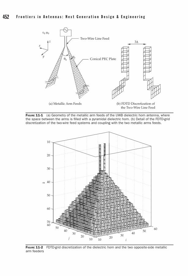
452 F r o n t i e r s i n a n t e n n a s : N e x t G e n e r a t i o n D e s i g n & e n g i n e e r i n g C h a p t e r 1 1 : N u m e r i c a l M e t h o d s i n a n t e n n a M o d e l i n g 453
Figure 11-1 (a) Geometry of the metallic arm feeds of the UWB dielectric horn antenna, where the space between the arms is filled with a pyramidal dielectric horn. (b) Detail of the FDTD-grid discretization of the two-wire feed systems and coupling with the two metallic arms feeds.
ε0 μ0
θhθf
x
y
zTwo-Wire Line Feed
Conical PEC Plate
(a) Metallic Arm Feeds
3Δ
(b) FDTD Discretization of the Two-Wire Line Feed
Figure 11-2 FDTD-grid discretization of the dielectric horn and the two opposite-side metallic arm feeders
1020
3040
5060
1020
3040
5060
10
20
30
40
50
60
70
ij
k
3040
50
2030
4050
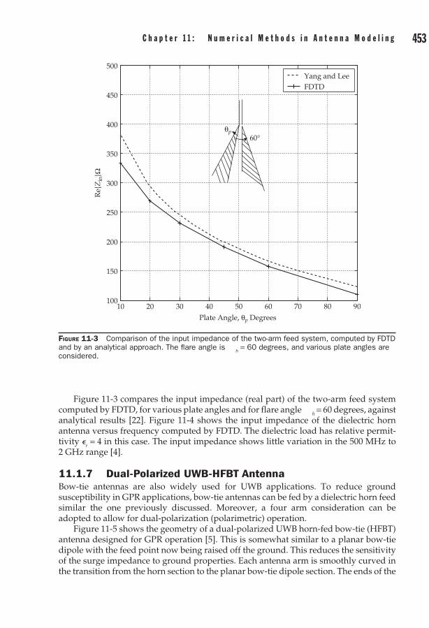
452 F r o n t i e r s i n a n t e n n a s : N e x t G e n e r a t i o n D e s i g n & e n g i n e e r i n g C h a p t e r 1 1 : N u m e r i c a l M e t h o d s i n a n t e n n a M o d e l i n g 453
Figure 11-3 compares the input impedance (real part) of the two-arm feed system computed by FDTD, for various plate angles and for flare angle σh = 60 degrees, against analytical results [22]. Figure 11-4 shows the input impedance of the dielectric horn antenna versus frequency computed by FDTD. The di electric load has relative permit-tivity r = 4 in this case. The input impedance shows little variation in the 500 MHz to 2 GHz range [4].
11.1.7 Dual-Polarized UWB-HFBT AntennaBow-tie antennas are also widely used for UWB applications. To reduce ground susceptibility in GPR applications, bow-tie antennas can be fed by a dielectric horn feed similar the one previously discussed. Moreover, a four arm consideration can be adopted to allow for dual-polarization (polarimetric) operation.
Figure 11-5 shows the geometry of a dual-polarized UWB horn-fed bow-tie (HFBT) antenna designed for GPR operation [5]. This is somewhat similar to a planar bow-tie dipole with the feed point now being raised off the ground. This reduces the sensitivity of the surge impedance to ground properties. Each antenna arm is smoothly curved in the transition from the horn section to the planar bow-tie dipole section. The ends of the
Figure 11-3 Comparison of the input impedance of the two-arm feed system, computed by FDTD and by an analytical approach. The flare angle is σ
h = 60 degrees, and various plate angles are
considered.
10 20 30 40 50 60 70 80 90100
150
200
250
300
350
400
450
500
Plate Angle, θp Degrees
Re
Zin
Ω
Yang and LeeFDTD
θp60°

454 F r o n t i e r s i n a n t e n n a s : N e x t G e n e r a t i o n D e s i g n & e n g i n e e r i n g C h a p t e r 1 1 : N u m e r i c a l M e t h o d s i n a n t e n n a M o d e l i n g 455
Figure 11-4 Input impedance of the horn-fed bow-tie antenna versus frequency computed by FDTD, for flare angle σ
h = 60 degrees and various plate angles (Source:[4], ©IEEE, 2004)
0.5 1 1.5 2−100
−50
0
50
100
150
200
250
300
350
400
Frequency in GHz
Impe
dan
ce Z
in Ω
10°20°30°40°50°60°
Figure 11-5 Illustration of the UWB-HFBT antenna geometry and dimensions
Coaxial CableR-card
PEC launcher
2.52 m0.63 m2.52 m
0.1 m
εr = 1.0
εr = 5.0
dipoles are terminated with tapered resistive cards (R-cards). The objective of the R-cards is to reduce reflections by gradually dissipating the currents propagating toward the end of each antenna arm. This increases the antenna bandwidth. The prototype considered here has a dielectric horn with r = 5. The plate angle of each antenna arm is 11.5 degrees. The horn angle itself is approximately 150 degrees.
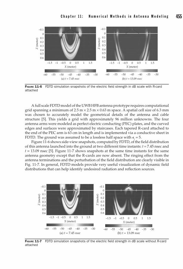
454 F r o n t i e r s i n a n t e n n a s : N e x t G e n e r a t i o n D e s i g n & e n g i n e e r i n g C h a p t e r 1 1 : N u m e r i c a l M e t h o d s i n a n t e n n a M o d e l i n g 455
A full scale FDTD model of the UWB HFB antenna prototype requires computational grid spanning a minimum of 2.5 m × 2.5 m × 0.63 m space. A spatial cell size of 6.3 mm was chosen to accurately model the geometrical details of the antenna and cable structure [5]. This yields a grid with approximately 96 million unknowns. The four antenna arms were modeled as perfect electric conducting (PEC) plates, and the curved edges and surfaces were approximated by staircases. Each tapered R-card attached to the end of the PEC arm is 63 cm in length and is implemented via a conductive sheet in FDTD. The ground was assumed to be a lossless half space with r = 5.
Figure 11-6 shows side-view snapshots, computed by FDTD, of the field distribution of this antenna launched into the ground at two different time instants: t = 7.45 nsec and t = 13.09 nsec [5]. Figure 11-7 shows snapshots at the same time instants for the same antenna geometry except that the R-cards are now absent. The ringing effect from the antenna terminations and the perturbation of the field distribution are clearly visible in Fig. 11-7. In general, FDTD models provide very useful visualization of dynamic field distributions that can help identify undesired radiation and reflection sources.
Figure 11-6 FDTD simulation snapshots of the electric field strength in dB scale with R-card attached
(a) t = 7.45 nsec (b) t = 13.09 nsec
–0.1
00.10.20.3
Z (m
eter
)
X (meter) X (meter)
0.40.50.6
–0.1
00.10.20.3
Z (m
eter
)
0.40.50.6
–1.5 –1 –0.5 0 0.5 1 1.5 –1.5 –1 –0.5 0 0.5 1 1.5
–30–35–40–45–50–55–60 –30–35–40–45–50–55–60
Figure 11-7 FDTD simulation snapshots of the electric field strength in dB scale without R-card attached
(a) t = 7.45 nsec (b) t = 13.09 nsec
–0.10
0.10.20.3
Z (m
eter
)
X (meter) X (meter)
0.40.50.6
–0.10
0.10.20.3
Z (m
eter
)
0.40.50.6
–1.5 –1 –0.5 0 0.5 1 1.5 –1.5 –1 –0.5 0 0.5 1 1.5
–30–35–40–45–50–55–60 –30–35–40–45–50–55–60

456 F r o n t i e r s i n a n t e n n a s : N e x t G e n e r a t i o n D e s i g n & e n g i n e e r i n g C h a p t e r 1 1 : N u m e r i c a l M e t h o d s i n a n t e n n a M o d e l i n g 457
11.1.8 Time-Domain Modeling of MetamaterialsIn recent years, there has been an upsurge in the design and development of new materials under the conceptual umbrella of “metamaterials,” as they show great promise to expand the design space of RF and optical devices and antennas. FDTD and FETD have proved to be quite effective tools for the analysis of metamaterials.
One interesting periodic material arrangement that provides a photonic crys tals (PhCs) with a degenerate band edge (DBE) is shown in Fig. 11-8a. In this arrangement, the unit cell has two misaligned anisotropic dielectric layers, A1 and A2, and one isotropic layer B. The dispersion relation can be tailored in order to produce a degenerate band edge by adjusting the thickness and permittivity of each layer. DBE PhCs can be designed to yield a (approximately) quartic dispersion relation just below the DBE frequency rather than the conventional quadratic dispersion relation present below a regular band edge (RBE). Fabry-Perot resonances (associated with narrowband transmission peaks) can be exploited in finite-size slabs made of such periodic stacks. Finite-size DBE PhCs are able to produce gigantic amplitude increase at Fabry-Perot resonances that have very good transmittance (matching) properties, which can be exploited by antennas operating in the resonance frequency [6].
Figure 11-8b shows the simulated transmission spectrum with the Fabry-Perot resonances below the DBE frequency, for N = 8 and N = 16, where N is the number of units cells. As N increases, the resonances move close to the DBE frequency (while the transmission bands are narrowed). As Fabry-Perot resonances move just below the band edge, a dramatic increase in field inten sity is produced because of slow wave effects (decrease in the group velocity). Hence, larger N leads to greater growth in field intensity. Figure 11-9 shows the FETD computed field distribution squared inside this metamaterial. Note that because the group velocity is smaller below the DBE frequency (from the quartic dispersion relation) than the RBE frequency (from the quadratic dis-persion relation), a much larger increase in the field amplitude is produced at DBE-based Fabry-Perot resonances than at the RBE counterpart for the same N.
Plasmon resonance structures have become the subject of intense study in recent years as potential building blocks of, among other devices, nanoantennas and (subwavelength) optical waveguides at the nanoscale (down to tens on nm). Localized
Figure 11-8 (a) Schematic of a DBE-PhC composed of two anisotropic dielec tric layers (A-layers) and one isotropic dielectric layer (B-layer). The dispersion relation can be tailored in order to produce a degenerate band edge by adjust ing the thickness and permittivity of each layer. (b) Associated transmission spectrum for different number of unit cells N (Source: [6], © Am. Phys. Soc., 2008).
(a) Periodic DBE Crystal Arrangement
0.9 0.92 0.94 0.96 0.98 1 1.020
0.10.20.30.40.50.60.70.80.9
1
Angular Frequency, ω [× c0]
Tran
smit
tanc
e
Semi-infinite8 unit cells16 unit cells
(b) Transmittance Spectrum
…
Eyinc
–Hxinc
x
yz
A1
LA1 LB LA2 Unit Cell
A1B BA2 A2

456 F r o n t i e r s i n a n t e n n a s : N e x t G e n e r a t i o n D e s i g n & e n g i n e e r i n g C h a p t e r 1 1 : N u m e r i c a l M e t h o d s i n a n t e n n a M o d e l i n g 457
surface plasmon resonances due to coherent electron oscillations excited at metal/dielectric interfaces yield highly localized field enhancement and provide guiding and confinement of electromagnetic waves well below the diffraction limit [7]. These structures are usually made of noble metals such as Ag and Au that exhibit dispersive response at optical frequencies, which can be modeled by ADE or PLRC techniques.
Figure 11-10 shows FDTD snapshots of the field intensity along a straight chain and a T-junction of a plasmon waveguide made of Au particles excited at center frequency of 580 THz. The excitation is a dipole located the left end of the waveguide. The particles
Figure 11-9 Steady-state (time-average) field intensity |E|2 inside a PhC with N = 16. The incident wave has unit amplitude. Increase in the field intensity is observed in DBE-PhC versus RBE-PhC (Source: [6], © Am. Phys. Soc., 2008).
0 2 4 6 8 10 12 14 160
20
40
60
80
100
120
Position
|E
|2
DBE PhCRBE PhC
Figure 11-10 (a) Snapshot of the field distribution computed along a linear chain plasmon waveguide at 516 nm. (b) Snapshot of the field distribution computed along a T-junction (see text for details).
(a) Linear Chain Waveguide (b) T-Junction
Ex @ 62.07729 ps
Ex @ 27.5 ps
0 100 200 300 400 500 600 0 100 200 300 400 500 600700 800 900 1000
X [nm] X [nm]
Y [n
m]
0
100
200
300
400
Y [n
m]
0
100
200
300
400
500
600
700
800
458 F r o n t i e r s i n a n t e n n a s : N e x t G e n e r a t i o n D e s i g n & e n g i n e e r i n g C h a p t e r 1 1 : N u m e r i c a l M e t h o d s i n a n t e n n a M o d e l i n g 459
are nanospheres with radius 25 nm and center-to-center spacing of 75 nm. The FDTD grid cell size has 1.5625 nm; 640 × 256 × 256 cells are used for straight chain and 448 × 544 × 256 cells for T-junction simulations. A Drude model is used to model the Au dielectric response in the frequency range considered. The corresponding wavelength is 516 nm, i.e., deep subwavelength guiding is achieved by these waveguides of lateral dimension 50 nm.
11.2 Frequency-Domain FEMGeometrical and material modeling flexibility of the FEM, has made it one of the most versatile design tools for modern antenna engineering. Recent advances in FEM modeling, coupled with fast and robust solution methods and general purpose mesh generation/graphical interface tools, have been instrumental in the proliferation of several commercial FEM packages in the past decade. Today, such commercial software are the antenna engineers’ most efficient tools in tackling modern antenna design chal-lenges. In this section, we outline the basic components of the FEM and sum marize some of the aspects that makes it a popular design tool for antenna engineering (see e.g., [23]–[26], [10] on FEM for antenna analysis).
The partial differential equations (PDEs) that govern “wave phenomena” is of particular interest to the antenna engineer for obvious reasons. Since a full review of Maxwell’s equations is beyond the scope of this chapter, we will simply focus on the time-harmonic wave equation to outline the FEM.
11.2.1 Weak Formulation of Time-Harmonic Wave Equa tionIn order to develop time harmonic FEM formulation, we will start by introducing the so-called “weak formulation” of the wave equation. For completeness, Maxwell equations in frequency domain (an e –iw t time convention is assumed and sup pressed) are
∇ × = ∇ × = − + ∇ = ∇ =E B H D j D Bi i eω ω ρ, , , ,· · 0 (11-43)
where E and H are the electric and magnetic field intensities, and D and B are the electric and magnetic flux densities, respectively. Also, J denotes the electric current density and σe is the electric charge density (related to electric current density via the continuity equation ∇ · J = iw σe). In addition, for linear anisotropic media, the electric and magnetic field intensities and flux densities are related through constitutive parameters, viz. D E= · and B H= µ · .
The wave equation for the electric field intensity is constructed by coupling Maxwell’s curl equations for the electric and magnetic field intensities. Namely, by taking the curl of Maxwell’s first equation (∇ × ∇ × E = iw ∇ × B) and then substituting Maxwell’s second equation (along with the constitutive relation B H= µ · ), we arrive at
∇ × ⋅ ∇ × − =−µ ω ω1 2( ( ) ( ) ( ) ( )r E r r E r J r) · i i (11-44)
where σ = 2π f denotes the angular frequency. In (11-44), Ji(r) represents the impressed excitations within the solution domain v. We remark that the right-hand side of (11-44) vanishes for source-free regions. A similar “dual” equation can also be obtained for the magnetic field intensity H(r).

458 F r o n t i e r s i n a n t e n n a s : N e x t G e n e r a t i o n D e s i g n & e n g i n e e r i n g C h a p t e r 1 1 : N u m e r i c a l M e t h o d s i n a n t e n n a M o d e l i n g 459
Equation (11-44) is a strong, point-wise condition that the electric field in tensity E must satisfy at all locations r within the domain of a given problem.
In general, as seen in Fig. 11-11, the solution domain may contain perfectly conducting and/or lossy surfaces, impedance boundaries, and homogeneous-isotropic/anisotropic materials, as well as inhomogeneous material regions. The versatility of the FEM stems from (11-44) in which material properties (e.g., linear, inhomoge neous, and anisotropic) are explicitly expressed.
Although as simple and as general (11-44) is, it is a mathematically strong statement whose solution cannot be readily obtained for arbitrary antenna ge ometries. However, this strong statement can be relaxed by seeking approximate field solutions that satisfy (11-44) in an average sense. Such an approximate form of (11-44) is mathematically called the “weak form.”
In order to relax the point-wise statement of (11-44), we proceed by defining auxiliary functions that will help us measure the error between the right- and left-hand sides of (11-44). Using a suitable inner product (please see [23], [10], [27]–[30] for a rigorous treatment) defined over the domain of the electric field E and a set of testing functions W = wj, j = 1 , . . . , N, we can rewrite (11-44) as
dv k i dvv
iv
W E E W J⋅ ∇ × ∇ × − =∫ ∫02 ωµ · (11-45)
where, for the sake of simplicity, we consider a linear, isotropic, and piecewise homogeneous domain, and the implicit r dependence is understood.
Our next step is to relax the double differentiation (i.e., double curl opera tion) requirement in (11-45). This is simply done using the vector identity
∇ × = ∇ × − ∇ ×· · ·( ) ( ) ( ),A B A B A B (11-46)
with A = W and B = ∇ × E, and (11-45) can be written as
dv dv k dv ivv
∇ × ∇ × − ∇ × ∇ × − =∫∫ · · · ( ) ( ) ( )W E W E W E02 ωµµ dv i
vvW J· .∫∫ (11-47)
Figure 11-11 Representation of a typical antenna problem involving multiple antennas and material regions
εr1εr2
(ε0, µ0)
µr3, εr3 εr4
V
Rload
Vin
S = ∂V
∼

460 F r o n t i e r s i n a n t e n n a s : N e x t G e n e r a t i o n D e s i g n & e n g i n e e r i n g C h a p t e r 1 1 : N u m e r i c a l M e t h o d s i n a n t e n n a M o d e l i n g 461
Next, Gauss theorem is applied to the first term of (11-47), which results in the weak form of the wave equation
dv k dv dsnvv s
( ) ( ) ˆ ( )∇ × ∇ × − − × ∇ ×∫∫ =W E W E W E· · ·0
2∂∂∫ ∫=v
iv
i dvωµ W J· . (11-48)
In (11-48), n in the outward normal vector on the boundary s = ∂ v. The surface integral can further be simplified using the vector identity
ˆ ( ) ( ˆ) ( ˆ ),n n n· · ·A B A B B A× = × = × (11-49)
resulting in the alternative expression
dv k dv ds nv v s
( ) ( ) ˆ ( )∇ × ∇ × − + × ∇ × =∫ ∫ ∫W E W E W E· · ·02 ii dv i
vωµ W J·∫ . (11-50)
The weak statements (11-48) and (11-50) must now be satisfied for a set of testing functions W. Hence, unlike (11-45), an approximate solution for E can be computed via the FEM.
It is also interesting to note that if we choose our testing function W to be the same as the electric field W = E (Galerkin testing, see [23], [10]), (11-48) becomes an energy conservation statement
dv k dv i dsnv v s
( ) ( ) ˆ ( )∇ × ⋅ ∇ × − ⋅ = ⋅ ×∫ ∫ ∫E E E E E H02 ωµ ++ ⋅∫i dv i
vωµ E J (11-51)
where the left-hand side is the total electric and magnetic energy contained in v and the right-hand side is the total power crossing s and power delivered into the volume by the impressed source.
The FEM seeks solutions to (11-48) and (11-50), which are weaker statements than (11-44), i.e., they are satisfied in an average sense over the whose solution space v. Thus, solutions E to (11-48) may not necessarily satisfy the original wave equation (11-44) exactly, only approximately. The construction of (11-48), starting from (11-44) and imposing (11-45) is called the weighted residuals method. Galerkin’s method, or Galerkin’s testing belongs to this family when the weighting functions is chosen to be the same as the unknown function, as was done in arriving at (11-51). Alternatively, one can arrive at the same weak form statement (also called the variational statement) through the Rayleigh-Ritz procedure, by minimizing the functional associated with the wave equation. Due to space limitations, the reader is referred to [23], [10] for more information on the functional approach in constructing the variational statement.
In the following, we seek solutions to the electric field intensity E in the domain v that satisfy (11-48) exactly, thus (11-44) weakly. Obviously, we can start by assuming a solution E and test (by choosing suitable testing functions W) whether this solution satisfies (11-48). However, since we can have infinitely many choices for assuming a solution E, this approach would rather inefficient. Alternatively, we may introduce a tessellation of the problem domain v via a connected mesh of simple shapes (triangular or quadrilateral finite elements for two-dimensional (2D) problems and tetrahedral or

460 F r o n t i e r s i n a n t e n n a s : N e x t G e n e r a t i o n D e s i g n & e n g i n e e r i n g C h a p t e r 1 1 : N u m e r i c a l M e t h o d s i n a n t e n n a M o d e l i n g 461
hexahedral finite elements for 3D) and express the unknown electric field intensity E as a sum of known functions with unknown coefficients, viz.
E r e r( ) ( ).==∑ ai ii
N
1
(11-52)
The “basis” functions, ei, i = 1 , . . . , N, are defined on the finite elements in terms of the local coordinates (to facilitate concise universal expressions). They should also respect the properties of the unknown electric field E. For instance, the vector-field nature of E should be respected by the choice of ei and conditions, such as ∇ × ei being well-defined must be satisfied.
Tetrahedral, hexahedral, and triangular-prism elements and associated basis functions are the most popular 3D finite elements used in antenna engineering. In the following section, we briefly summarize the usual 2D and 3D finite elements.
11.2.2 Geometry Modeling and Finite-Element RepresentationsAs noted above, the first step in implementing the FEM to analyze a radiating structure is to approximate the antenna geometry and the surrounding solution domain v by a connected mesh of geometrically simple elements (see Fig. 11-12). This mesh forms an approximation to the solution domain, and basis functions are expressed directly on the mesh elements. Some popular choices for 2D elements are depicted in Fig. 11-13, and those for 3D elements are shown in Fig. 11-14. For example, a 2D triangular element is defined by its three vertices r1, r2, r3, as shown in Fig. 11-15. Any point r inside the element has the barycentric coordinates (ζ1, ζ2, ζ3) where ζi is defined with respect to the area of each subtriangle formed by connecting r to the vertices, viz. ζi = Ai /A, where A = A1 + A2 + A3 is the area of the triangle. Similarly, 4 barycentric variables can be constructed for tetrahedral elements.
Figure 11-12 FEM meshes of the Vivaldi antenna using (a) tetrahedral ele ments, (b) triangular-prism elements, and (c) hexahedral elements
(a)
X Y
Z
(b) (c)
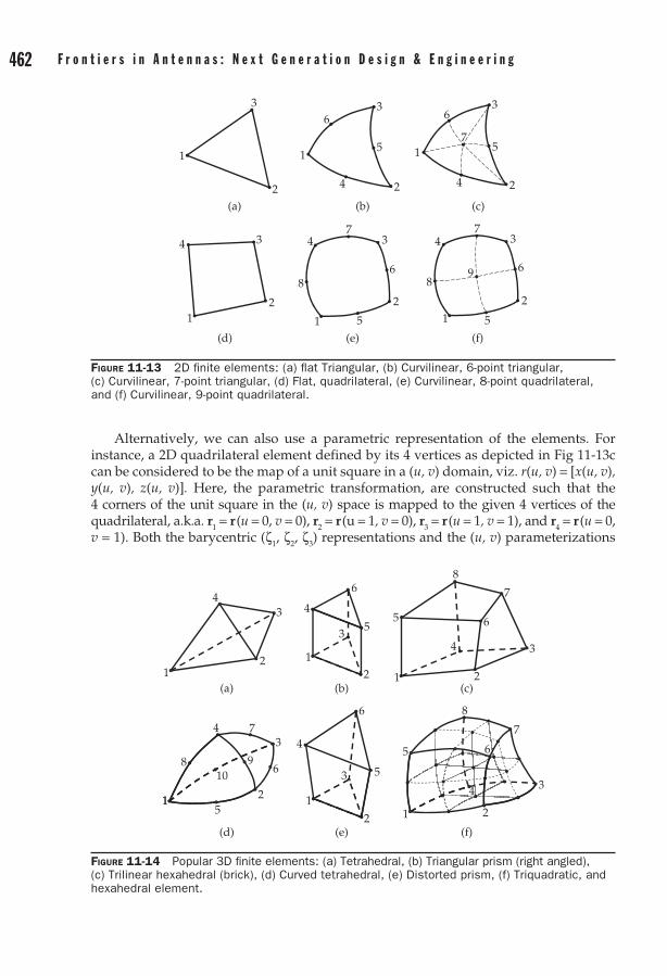
462 F r o n t i e r s i n a n t e n n a s : N e x t G e n e r a t i o n D e s i g n & e n g i n e e r i n g C h a p t e r 1 1 : N u m e r i c a l M e t h o d s i n a n t e n n a M o d e l i n g 463
Alternatively, we can also use a parametric representation of the elements. For instance, a 2D quadrilateral element defined by its 4 vertices as depicted in Fig 11-13c can be considered to be the map of a unit square in a (u, v) domain, viz. r(u, v) = [x(u, v), y(u, v), z(u, v)]. Here, the parametric transformation, are constructed such that the 4 corners of the unit square in the (u, v) space is mapped to the given 4 vertices of the quadrilateral, a.k.a. r1 = r (u = 0, v = 0), r2 = r (u = 1, v = 0), r3 = r (u = 1, v = 1), and r4 = r (u = 0, v = 1). Both the barycentric (ζ1, ζ2, ζ3) representations and the (u, v) parameterizations
Figure 11-13 2D finite elements: (a) flat Triangular, (b) Curvilinear, 6-point triangular, (c) Curvilinear, 7-point triangular, (d) Flat, quadrilateral, (e) Curvi linear, 8-point quadrilateral, and (f) Curvilinear, 9-point quadrilateral.
1
2(a) (b) (c)
(f)(e)(d)
3
1
2
3
4
5
6
1
24
5
6
7
3
1
2
34
5
6
7
89
12
34
1
2
34
5
6
7
8
Figure 11-14 Popular 3D finite elements: (a) Tetrahedral, (b) Triangular prism (right angled), (c) Trilinear hexahedral (brick), (d) Curved tetrahedral, (e) Dis torted prism, (f) Triquadratic, and hexahedral element.
12
3
4
5
6
3
4
5
6
1 2
34
5 6
7
8
34
5 6
7
8
12
34
1 2
34
6
7
8 910
1
2 1 21
5
(a) (b) (c)
(f)(e)(d)

462 F r o n t i e r s i n a n t e n n a s : N e x t G e n e r a t i o n D e s i g n & e n g i n e e r i n g C h a p t e r 1 1 : N u m e r i c a l M e t h o d s i n a n t e n n a M o d e l i n g 463
allow for simple expressions for the elements and the basis functions defined on these elements. This simplicity is particularly useful for implementation ease. Representations of 3D tetrahedral, hexahedral, and triangular-prism elements are summarized in the following subsections. Curvilinear versions of such elements can be found in various journal papers [31]–[33].
11.2.2.1 Tetrahedral ElementsThe position vector r inside the tetrahedral element is given in terms of the 4 barycentric parameters, ζi, defined by connecting the position vector to the 4 vertices defining the element. Each barycentric variable is defined as ζi = Vi /V, where Vi is the volume of the subtetrahedron defined by the position vector r and the face of the tetrahedron across the ith vertex, and V is the volume of the element V = V1 + V2 + V3 + V4 (see Fig. 11-16).
11.2.2.2 Hexahedral ElementsMuch like the 2D quadrilateral elements, 3D hexahedra can be simply defined as a mapping of a unit cube in the parametric (u, v, w) space, viz.
r r( , , ) ( ) ( ) ( )u v w L u L v L wi j k ijkkji
====
∑∑∑1
2
1
2
1
2
(11-53)
Figure 11-15 Parametric representations of 2D finite elements: (a) Barycentric coordinates for a triangular element, (b) (u, v) parametrization of a quadrilat eral.
r1
r2
r3
r(ζ1, ζ2, ζ3)
A1A3
A2
r1
r2
r3r4
r(u0, v0)
u
v
(a) (b)
Figure 11-16 3D tetrahedral element
1
3
2
1
6
5 4
2
3
4
r(ζ1, ζ2, ζ3, ζ4)

464 F r o n t i e r s i n a n t e n n a s : N e x t G e n e r a t i o n D e s i g n & e n g i n e e r i n g C h a p t e r 1 1 : N u m e r i c a l M e t h o d s i n a n t e n n a M o d e l i n g 465
where rijk i = 1, 2; j = 1, 2; and k = 1, 2 are the 8 vertices of the element as shown in Fig. 11-17. Also, L1(τ) = τ and L2(τ) = 1 – τ, are the first-order Lagrange interpolators for τ = u, v, w. We also note that for (11-53) to be valid, the vertices of the element must lie on a topologically rectangular grid.
11.2.2.3 Triangular-Prism ElementsThe distorted triangular-prism element [34] shown in Fig. 11-18 can be repre sented in terms of the parametric height variable t in addition to the barycentric (ζ1, ζ2, ζ3) coordinates of the triangular faces, viz.
r r r r r r( , , , ) ( ) ζ ζ ζ ζ ζ ζ ζ1 2 3 1 1 2 2 3 3 1 41t t= + + − + + 55 2 6 3ζ ζ+ r t (11-54)
Figure 11-17 3D hexahedral element and the illustrations of covariant and contravariant basis vectors
1 4
8 4
2
10
1
2
33
7
5
12
6
6
5
9
7
8
au
av
aw
aw
au
av
11
Figure 11-18 Triangular-prism element and the illustration of its parametric representation
1
7
3
82
1
4
6
5
9
2
3
4
5
6
r(ζ1, ζ2, ζ3, t)

464 F r o n t i e r s i n a n t e n n a s : N e x t G e n e r a t i o n D e s i g n & e n g i n e e r i n g C h a p t e r 1 1 : N u m e r i c a l M e t h o d s i n a n t e n n a M o d e l i n g 465
where ri, i = 1 , . . . , 6 are the 6 vertices of the distorted prism. As a special case of the distorted prism element, the right-angled prism element is particularly useful in for layered media, often encountered in modeling antennas.
The previous definitions provide the mathematical tools to represent the finite elements. Next, we summarize some popular vector basis functions defined on these finite elements to express the electric field unknowns in FEM.
11.2.3 Vector Finite ElementsFor programming simplicity, it is desirable to use low-order polynomial expres sions to construct the basis functions. As such, the following are among the most widely utilized in FEM for antenna modeling [35].
11.2.3.1 Vector Basis Functions on TetrahedraAssociated with each of the 6 edges of the tetrahedral element, we define 6 basis functions expressed in terms of the barycentric coordinates. Assuming a local edge numbering given in Table 11-1, the basis function associated with the kth edge is given as
ek ij i j j il i j= ∇ − ∇ =( ), , , , ,ζ ζ ζ ζ 1 4L (11-55)
where lij = lk is the length of the edge between the vertices i and j forming the kth edge. It can be shown that ∇ · ek = 0 and ∇ × ek = lij 2∇ζi × ∇ζj.
11.2.3.2 Vector Basis Functions on HexahedraOne can define the basis function for hexahedral elements in a slightly different manner, in the parametric (u, v, w) space. To do so, we start by introducing partial derivatives (a.k.a. parametric covariant vectors) aτ = ∂r/ ∂τ where τ = (u, v, w). Next, we define a complementary set of vectors, namely the contravariant vectors as
a a a a a a a a auv w
vw u
wu vV V V
= × = × = ×+ + +
1 1 1, , , (11-56)
Local Edge Number First Node Second Node
1 1 2
2 1 3
3 1 4
4 2 3
5 4 2
6 3 4
Table 11-1 Local Edge Numbering for a Tetrahedral Element

466 F r o n t i e r s i n a n t e n n a s : N e x t G e n e r a t i o n D e s i g n & e n g i n e e r i n g C h a p t e r 1 1 : N u m e r i c a l M e t h o d s i n a n t e n n a M o d e l i n g 467
where V+ = au · (av × aw) is the differential volume used for normalization. Using these contravariant vectors, first-order vector finite-element functions can be written as
e a e a
e a e
1 2
3 4
1
1
= = −
= − =
( )( ) , ( )( )
( )( ) , (
v w v w
v w
u u
u 11 1
15 6
7
− −
= = −
=
v w
u w u w
u
u
v v
)( )
( )( ) , ( )( )
( )
a
e a e a
e (( ) , ( )( )
( )( ) , (
1 1 1
1
8
9 10
− = − −
= = −
w u w
u v
v v
w
a e a
e a e uu v
u v u v
w
w w
)( )
( )( ) , ( )( ) .
a
e a e a11 121 1 1= − = − −
(11-57)
Curls of the above functions can be easily evaluated using the standard formula
∇ × =∂ ⋅
∂−
∂ ⋅∂
+
∂ ⋅e
e a e aa
e ai
i w i vu
i
g v w1 ( ) ( ) ( uu i w
v
i v
w v
u
) ( )
( ) (
∂−
∂ ⋅∂
+∂ ⋅
∂−
∂
e aa
e a ee aai u
wv⋅
∂
)
(11-58)
where g is the determinant of the metric tensor
gu u u v u w
v u v v v w=⋅ ⋅ ⋅⋅ ⋅ ⋅
( ) ( ) ( )( ) ( ) (a a a a a aa a a a a a ))
( ) ( ) ( ).
a a a a a aw u w v w w⋅ ⋅ ⋅ (11-59)
For a rectangular hexahedral element (a.k.a. the brick element), the above expressions can be simplified via au = au = r2 – r1, av = av = r4 – r1, and aw = aw = r5 – r1. In addition, the metric tensor determinant becomes g V= where V is the volume of the rectangular prism. Subsequently, the curls of the brick element basis functions also simplify as
∇ × = −
∇ × = − −
∇ × =
e a a
e a a
e
1
3
5
1
11
Vv w
Vv w
v w
v w
,
( ) ,
11
11
17
9
Vw u
Vw u
Vu
w u
w u
,
( ) ,
a a
e a a
e
−
∇ × = − −
∇ × = aa a
e a a
e
u v
u v
v
Vu v
Vv
−
∇ × = − −
∇ × = −
,
( ) ,
(
11
2
11
11 )) ,
( ) ( ) ,
a a
e a a
e
v w
v w
w
Vv w
V
−
∇ × = − − −
∇ × =
4
6
11 1
1ww u
Vw u
w u
w u
a a
e a a
e
− −
∇ × = − − −
∇ ×
( ) ,
( ) ( ) ,
1
11 18
100
12
11
11 1
= − −
∇ × = − − −
Vu v
Vu v
u v
u v
( ) ,
( ) ( )
a a
e a a ,
(11-60)
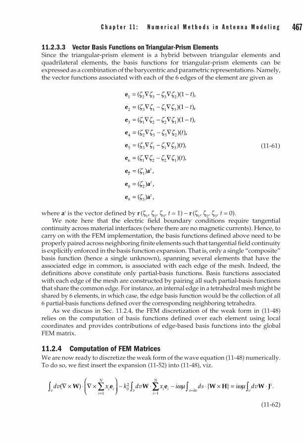
466 F r o n t i e r s i n a n t e n n a s : N e x t G e n e r a t i o n D e s i g n & e n g i n e e r i n g C h a p t e r 1 1 : N u m e r i c a l M e t h o d s i n a n t e n n a M o d e l i n g 467
11.2.3.3 Vector Basis Functions on Triangular-Prism ElementsSince the triangular-prism element is a hybrid between triangular elements and quadrilateral elements, the basis functions for triangular-prism elements can be expressed as a combination of the barycentric and parametric representations. Namely, the vector functions associated with each of the 6 edges of the element are given as
e
e
1 2 3 3 2
2 3 1 1 3
1
1
= ∇ − ∇ −
= ∇ − ∇ −
( )( ),
( )( )
ζ ζ ζ ζ
ζ ζ ζ ζ
t
t ,,
( )( ),
( )( )
e
e
3 1 2 2 1
4 2 3 3 2
1= ∇ − ∇ −
= ∇ − ∇
ζ ζ ζ ζ
ζ ζ ζ ζ
t
t ,,
( )( ),
( )( ),
e
e
e
5 3 1 1 3
6 1 2 2 1
= ∇ − ∇
= ∇ − ∇
ζ ζ ζ ζ
ζ ζ ζ ζ
t
t
77 1
8 2
9 3
=
=
=
( ) ,
( ) ,
( ) ,
ζ
ζ
ζ
a
e a
e a
t
t
t
(11-61)
where at is the vector defined by r (ζ1, ζ2, ζ3, t = 1) – r (ζ1, ζ2, ζ3, t = 0).We note here that the electric field boundary conditions require tangen tial
continuity across material interfaces (where there are no magnetic currents). Hence, to carry on with the FEM implementation, the basis functions defined above need to be properly paired across neighboring finite elements such that tangential field continuity is explicitly enforced in the basis function expansion. That is, only a single “composite” basis function (hence a single unknown), span ning several elements that have the associated edge in common, is associated with each edge of the mesh. Indeed, the definitions above constitute only partial-basis functions. Basis functions associated with each edge of the mesh are constructed by pairing all such partial-basis functions that share the common edge. For instance, an internal edge in a tetrahedral mesh might be shared by 6 elements, in which case, the edge basis function would be the collection of all 6 partial-basis functions defined over the corresponding neighboring tetrahedra.
As we discuss in Sec. 11.2.4, the FEM discretization of the weak form in (11-48) relies on the computation of basis functions defined over each element using local coordinates and provides contributions of edge-based basis functions into the global FEM matrix.
11.2.4 Computation of FEM MatricesWe are now ready to discretize the weak form of the wave equation (11-48) numerically. To do so, we first insert the expansion (11-52) into (11-48), viz.
dv x k dv xv i i
i
N
i ii
N
( )∇ × ⋅ ∇ ×
− ⋅∫ ∑= −
W e W e1
02
1∑∑∫ ∫∫− ⋅ × = ⋅
=∂vi
vs vi ds i dvωµ ωµ .W H W J
(11-62)

468 F r o n t i e r s i n a n t e n n a s : N e x t G e n e r a t i o n D e s i g n & e n g i n e e r i n g C h a p t e r 1 1 : N u m e r i c a l M e t h o d s i n a n t e n n a M o d e l i n g 469
In order to be able to construct a linear system for the N unknowns, we next choose N testing functions wj, j = 1 , . . . , N, giving
x dv k x dvi
i
N
j iv ii
N
j iv= =∑ ∫ ∑∇ × ⋅ ∇ × − ⋅
102
1
( ) ( )w e w e∫∫ ∫
∫
− ⋅ ×
= ⋅ =
=∂i d
i dv j N
s v j
jvi
ωµ
ωµ
s w H
w J K
, , ,1
(11-63)
which can be written in a compact matrix form [Z] x = f . However, note that the surface integral contribution is written in terms of the surface magnetic field, which itself is an unknown. Thus the boundary magnetic field H must be dealt with before we can transform (11-63) into a matrix equation. Several efficient methods of mesh truncation are addressed next.
11.2.4.1 Truncation of the Solution Domain
11.2.4.1.1 Absorbing Boundary Conditions The simplest and one of the most popular methods for mesh truncation for wave equation is to simply impose the far-field behavior of fields as the boundary condition on the surface mesh bounding the FEM domain. As is well-known, fields radiating away from a source can be approximated as locally planar spherical waves in the far zone. That is, the following relation holds for the tangential components of electric and magnetic field intensities:
ˆ ( ) ˆ ˆ ( ).n ik n n× = × ×H r E rscat scat0 (11-64)
The above condition approximately applies for the mesh truncation surface if it is sufficiently away from the sources and/or scattering centers within the FEM domain. However, since the total field within the domain just inside the truncation boundary consists of incident and scattered fields, (11-64) must be modified as
ˆ ( ) ˆ ˆ ( ) ˆ ( ) ˆ ˆn ik n n n ik n× − × × = × − ×H r E r H r0 0inc nn × E rinc ( ). (11-65)
Using (11-65), the unknown H under the surface integral in (11-50) can be written in terms of the electric field intensity E(r) as
ds ds n
ds
s v s v
s v
⋅ × = − ⋅ ×
= −
=∂ =∂
=∂
∫ ∫
∫
ˆ W H W H
W ⋅⋅ × × + × − × × ˆ ( ˆ ) ˆ ˆ ( ˆ ).ik n n n ik n n0 0E H Einc inc
(11-66)
Next, we transfer the first term involving the unknown E to the left-hand side of (11-48) and the terms involving the known incident field to the right-hand side. Doing so, (11-48) becomes
dv k dv ik ds n n
v v( ) ( ) [ ˆ ( ˆ∇ × ⋅ ∇ × − ⋅ + ⋅ × ×∫ ∫W E W E W E0
20 ))]
( ˆ ) [ ˆ
s
vii dv ds n ik ds n
∫
∫= ⋅ − ⋅ × + ⋅ωµ W J W H Winc0 ×× ×∫∫ ( ˆ )].n
ssEinc
(11-67)

468 F r o n t i e r s i n a n t e n n a s : N e x t G e n e r a t i o n D e s i g n & e n g i n e e r i n g C h a p t e r 1 1 : N u m e r i c a l M e t h o d s i n a n t e n n a M o d e l i n g 469
Alternatively, this can be cast in a more symmetric form as
dv k dv ik ds n n
v v( ) ( ) ( ˆ ) ( ˆ∇ × ⋅ ∇ × + ⋅ − × ⋅ ×∫ ∫W E W E W0
20 EE
W J W H W
)
( ˆ ) ( ˆ
s
vii dv ds n ik ds n
∫
∫= ⋅ − ⋅ × − ×ωµ inc0 )) ( ˆ ).⋅ ×∫∫ n
ssEinc
(11-68)
In the above, the right-hand side is recognized the total excitation, consisting of an incident field excitation due to known sources external to the FEM domain as well as impressed currents within the FEM domain.
Discretization of the above equation as in (11-62) results in a sparse FE matrix. As mentioned earlier, as long as the truncation surface is sufficiently away (such that the electromagnetic fields locally behave as outward traveling plane waves), the absorbing boundary condition (ABC) approximation gives sufficiently accurate results. In discretized form, the FE-ABC equations are given as
E EE E
aa
ff
VV SV
VS SSV
S
I
S
=
, (11-69)
where
E dv k dvVVjv i jv i= ∇ × ⋅ ∇ × − ⋅∫ ∫( ) ( )e e e e0
2 (11-70)
for all finite-element edges inside the solution domain v, and
E E dv k dvSV VS T
jv i j iv= = ∇ × ⋅ ∇ × − ⋅∫ ∫[ ] ( ) ( )e e e e0
2 (11-71)
for all basis functions ei in the volume v and testing functions ej associated with the edges on the boundary surface s. More importantly, the surface unknown contributions in (11-69) are given as
E dv k dv ik ds nSSjv i j i= ∇ × ⋅ ∇ × − ⋅ − ×∫ ( ) ( ) ( ˆe e e e e0
20 jjsv in) ( ˆ ).∫∫ ⋅ × e (11-72)
In addition, all excitations inside the FEM volume v contribute to the first part of the right-hand side and are computed using
f i dvI iv
= ⋅∫ωµ W J . (11-73)
Moreover, the surface portion of the excitation vector [ f I f S]T in (11-69) may also contain external incident field contributions in the form
f ds n ik ds n nSjv is
= − ⋅ × − × ⋅ ×∫ ∫e H e E( ˆ ) ( ˆ ) ( ˆinc in0
ccinternal) ,+ f S (11-74)
in which any internal sources on the truncation boundary also contribute to the right-hand side, viz.
f i dvSv
i sinternal = ⋅∫ωµ W J , . (11-75)

470 F r o n t i e r s i n a n t e n n a s : N e x t G e n e r a t i o n D e s i g n & e n g i n e e r i n g C h a p t e r 1 1 : N u m e r i c a l M e t h o d s i n a n t e n n a M o d e l i n g 471
Excitations interior to the solution domain are typically used to model port excitations in antenna design. These include infinitesimal voltage and current sources, as well as waveguide feed ports. We will summarize such excitations in Section 11.2.5.
All integrations involved in (11-70)–(11-75) can be evaluated numerically using a suitable quadrature. However, in most cases closed form expressions using the definitions of the basis functions can also be obtained.
Turning our attention back to mesh truncations schemes, we note that the approxi-mate ABC in (11-65) is sometimes referred to as the zeroth order ABC (or the radiation boundary condition) since it involves only the far-field behavior of the electromagnetic energy. Several higher-order ABCs have also been developed for improved accuracy (see e.g., [36], [37], [15], [23], [10]). Such higher-order ABCs allow one to bring the FEM truncation surface closer to the antenna struc ture, thereby keeping the FEM domain and the resulting FEM matrix equation small, leading to faster and more efficient solu-tions. Another alternative to keep the FEM mesh close to the antenna structure is to use perfectly matched layers, which are discussed below.
11.2.4.1.2 Artificial Absorbers and Perfectly Matched Layers Much like the ABCs, artifi-cial absorbers are simply artificial material layers that are placed on the truncation surface inside the FEM mesh. When the surface integral in (11-50) over the truncations surface s is simply discarded, the boundary sur face ends up behaving like a conduct-ing surface (the surface integral equals zero when Etan = 0). Artificial absorbers are placed over this PEC boundary to eliminate reflections back into the solution domain. As such, multiple layers to artificial lossy materials with equal relative permittivity and permeabilities i = µi (for wave impedance matching) are placed on the inside of the truncation surface. The thicknesses and the material parameters are arranged such that the reflection from the truncation surface is minimized over a broad frequency and incidence angle range. The process of designing such artificial absorbers often re-quires a multidimensional optimization and results in nonphysical material parame-ters for the layers [23], [10]. A particular set of artificial absorbers, perfectly matched layers, is rather popular in FEM modeling (as well as in time-domain FEM and finite-difference implementations).
Perfectly matched layers [15] are artificial, anisotropic lossy material layers that do not reflect waves impinging from a lossless medium. Formal derivation of various PMLs is lengthy and beyond the scope of this introductory chapter and can be found in most prominent finite-element books such as [23], [10]. With the predetermined PML material parameters, the FE equation (using anisotropic material formulation)
dv dv i dvv
ivv
( ) ( )∇ × ⋅ ⋅ ∇ × − ⋅ ⋅ = ⋅− ∫ ∫∫ W E W E W Jµ ω ω1 2 (11-76)
can be solved straightforwardly without the need to deal with the surface fields on s.Several combinations of ABCs and PMLs have also been considered. In particular,
ABC backed PMLs provide better absorption of outgoing energy. Also, averaging two solutions to the same problem, one with with PMC backed PML and the other with the conventional PEC backed PML, can provide much better accuracy.
11.2.4.1.3 Exact Mesh Termination Through Boundary Integral Equations In addition to the mesh truncations summarized above, an exact relation between the tangential

470 F r o n t i e r s i n a n t e n n a s : N e x t G e n e r a t i o n D e s i g n & e n g i n e e r i n g C h a p t e r 1 1 : N u m e r i c a l M e t h o d s i n a n t e n n a M o d e l i n g 471
electric and magnetic fields on the truncations surface can be used. These are given in terms of the Stratton-Chu integral representa tion formulas [38]. Namely, the electric field integral equation (EFIE) is given by
12
ˆ ( ˆ ) ˆ [ ˆ ( ˆ )] ˆ [ ˆ ( ˆ )]n n n n n n n n× × + × × × + × × ×E H EL K == × ×ˆ ( ˆ ),n n Einc (11-77)
and the magnetic field integral equation (MFIE) is given by
12
ˆ ˆ ( ˆ ) ˆ ( ˆ ) ˆ ,n n n n n n× + × × − × × = ×H H E HK L inc (11-78)
where the operators L and K are defined as
L( )X X X= − + ∇ ′∇ ⋅
∫ik ds
ke
Rs
ik R
002
14
0
π (11-79)
and
K( ) ,X X= × ∇∫ dse
Rs
ik R0
4π (11-80)
in which R = |r – r’| is the distance between the source and observation points. Both (11-77) and (11-78) are exact relations between the tangential field components; however, while the ABC relation n × H = ik0
n × (n × E) was used to eliminate n × H in (11-48) before, in this case the unknown n × H appears under integral operators. Thus, a simple elimination is not possible. Nonetheless, we can treat n × H as an unknown as it is and use the EFIE or the MFIE as an additional equation to complement the original FEM system. However, we must note that care must be taken in doing so since both (11-77) and (11-78) are themselves prone to so-called interior resonance problems. To eliminate this problem, a weighted sum of EFIE and MFIE, called the combined field integral equation, is used. The resulting FE-BI system is compactly given as
E EE E B
B Z
EEH
VV SV
VS SSV
S
S
0
0 %
=
JJb
I
S . (11-81)
In the above, the submatrices EVV, ESV, and EVS are identical to those given in (11-70) and (11-71). However, the submatrix ESS in (11-81) is slightly modified in that the surface integral in (11-72) is treated separately as a submatrix B, viz.
E dv k dv
B ik ds
SSj iv j iv
= ∇ × ⋅ ∇ × − ⋅
= −
∫ ∫( ) ( )
(
e e e e02
0ˆ ) ( ˆ ).n niS j× ⋅ ×∫ e e
(11-82)

472 F r o n t i e r s i n a n t e n n a s : N e x t G e n e r a t i o n D e s i g n & e n g i n e e r i n g C h a p t e r 1 1 : N u m e r i c a l M e t h o d s i n a n t e n n a M o d e l i n g 473
In addition, the boundary integral equation submatrices %B and Z are given in terms of the EFIE and MFIE contributions as % % %B B B= + (1 – )EFIE MFIEα α and Z = aZEFIE + (1 – a) ZMFIE, where a is a constant between 0 and 1, typically chosen as 0.5 and
%B ds n n n n njS i iEFIE = × ⋅ × × + × ×∫ ( ˆ ) ˆ ( ˆ ) ˆ ( ˆ )t e e12
K
= − × ⋅ × ×∫%B ds n n n
Z
jS iMFIE
EF
( ˆ ) [ ˆ ( ˆ )]t eL
IIE
MFIE
= × ⋅ × × ×
=
∫ ds n n n n
Z ds n
jS i( ˆ ) ˆ [ ˆ ( ˆ )]
( ˆ
t hL
×× ⋅ × + × ×
∫ t h hjS i in n n) ( ˆ ) ˆ ( ˆ ) .
12
K
(11-83)
Here, we also introduced the testing functions tj defined over the surface ele ments on s. Moreover, for the CFIE implementation, the excitations submatrix b associated with external excitations is also given as
b ds n n n ds njS j= × ⋅ × × + − × ⋅∫α α( ˆ ) ˆ ( ˆ ) ( ) ( ˆ )t E tinc 1 ˆnS
×∫ Hinc (11-84)
Although the previous equations seem complicated, they can be greatly sim plified when the surface basis/testing functions for the tangential electric and magnetic field are chosen to be the same such that ej = hj. Also, tj is chosen as tj = n × hj on the surfaces of volumetric elements that lie on the bound ary S. We also note that several variants of the FE-BI system have also been reported [39]–[42].
In numerically solving real-life problems, one would like to be assured that the obtained FEM solution is accurate. In essence, if a solution is obtained using an FEM mesh with an average edge length of h, it is important to put an upper bound on the error in the FEM solution in terms of the mesh parameter h. That is, we expect that FEM solution accuracy should improve when a denser mesh is used for the same problem. To measure a rate of convergence, the mesh parameter h is used. Another alternative is to improve the modeling abilities of the basis functions using higher-order expansions [43]–[47]. If we denote the FE expansion order with p, we must be assured that by increasing p the FEM error can be improved. Obviously, a denser mesh or a higher-order expansion is most beneficial in the regions where the field behavior changes rapidly due to sharp geometrical changes, such as edges and corners, or due to excitations points, such as feeds and waveguide ports. Thus, often both strategies are combined and mesh density and basis function order are adaptively increased over regions with rapid spatial field variations [48].
11.2.5 Feed ModelingFor an accurate antenna analysis, it is important that the antenna feeds within the FEM domain are accurately representable in the FEM statement. In addition to material modeling capabilities, the FEM also incorporates various feeding mechanisms used in modern antenna designs. Some of the most frequently used feed models are summarized in the following subsections.

472 F r o n t i e r s i n a n t e n n a s : N e x t G e n e r a t i o n D e s i g n & e n g i n e e r i n g C h a p t e r 1 1 : N u m e r i c a l M e t h o d s i n a n t e n n a M o d e l i n g 473
11.2.5.1 Current Probe FeedsCoaxial transmission lines are widely used in printed antennas, such as microstrip patch antennas. Typically, the center conductor of the coaxial feed is attached to the patch and the outer conductor to the ground plane. The short section of the center conductor behaves as a current probe that excites the patch antenna. Such feeds can readily be modeled with FEM when this short section is treated as an impressed current source under the patch. As such, the coaxial transmission line is replaced by a current probe feed and the excitation of this current probe is computed by
f ik Z dvI iVs
= ⋅∫0 0 W J (11-85)
where the impressed current source is due to a current element along the direc-tion of the original coaxial probe as
J r= ˆ ( ).lI sδ (11-86)
The input impedance of the feeding port can be subsequently found by consid-ering the electric field unknown (after solving the FEM system) at the probe feed location using the well-known formula Zin = V/I, where
V dl ll
= − ⋅∫ E ˆ (11-87)
in which l is the length of the probe section.Alternatively, for modeling antennas fed by other types of transmission
lines, such as dipole antennas, a voltage gap model may be more appropriate.
11.2.5.2 Voltage Gap FeedsIf we assume a voltage differential exists across the pth edge of the FEM mesh, such that the electric field across the edge is forced to assume a constant value, we can eliminate the unknown associated with that edge through Es = V/d, where d is the length of the edge. With this assignment, the column in the FEM matrix associated with the voltage gap edge can be explicitly evaluated and thus is eliminated from the system, decreasing the matrix size by 1 for each voltage gap source. Consequently, the pth column becomes an excitation to the reduced system as
bVd
dvk V
ddvj j pv j pv
= ∇ × ⋅ ∇ × + ⋅∫ ∫( ) ( ) .w e w e02
(11-88)
After the solution of the reduced system, the input impedance of the voltage gap excitation port can be found from Zin = V/I, where the current I flowing across the voltage gap feed can be found by
II
idl c
c= ∇ × ⋅∫ωµ
( ) ˆ.E (11-89)
474 F r o n t i e r s i n a n t e n n a s : N e x t G e n e r a t i o n D e s i g n & e n g i n e e r i n g C h a p t e r 1 1 : N u m e r i c a l M e t h o d s i n a n t e n n a M o d e l i n g 475
11.2.5.3 Lumped Circuit ElementsLumped elements can also be easily implemented by assigning lossy/reactive material parameters to the finite elements associated with the circuit components. For example, a lumped load of impedance ZL associated with the kth edge of the mesh contributes to the FEM via
Eik Z l
ZVV
L
=− 0 0
2
(11-90)
As such, modeling of shorting pins is extremely easy in the sense that for each shorting pin edge, simply the associated edge unknown is set to zero, eliminating the associated column from the FEM matrix.
11.2.5.4 Waveguide Port FeedsFor modeling antennas that are fed via waveguides, a modal expansion must be incorporated into the FEM system. This is needed to express the surface H field over the waveguide port in terms of the unknown E field (so that the surface term in (11-48) can be eliminated). For this, a general modal summation expression for the waveguide fields, given as
H h E E e= + = +∑ ∑Hinc inca eaZ
em mm
m
m
mm
m
m
z zγ γ, (11-91)
where
a e dsmm
mS z L
L= ⋅ −−=∫γ h H H[ ]inc (11-92)
is used. Obviously, various orthonormality relationships between waveguide modes can be applied to simplify the above equation [23], [10], [38].
Although we stated the eigenmode expansion using infinitely many modes, the summations in (11-92) are truncated in FEM implementations. If the waveguide port surface inside the waveguide is chosen far enough from the waveguide-antenna junction, only a few terms in (11-92) is sufficient since most higher-order modes are evanescent and will die out before reaching the wave-port surface. Moreover, the wave-port can be chosen sufficiently far from the junction such that considering only the dominant mode would result in accurate FEM solu tions. Since waveguides are typically small in size, the additional burden to model the extra waveguide section in the FEM domain is often very small.
In addition to the feed models summarized above, known incident fields from sources external to the solution domain can also be included as excitations using (11-74) and (11-84) for the FE-ABC and FE-BI implementations, respectively. Moreover, FEM problems involving thin lossy material layers and/or con ductors coated with thin layers can be further simplified by replacing such thin layers by equivalent impedance boundary conditions. Resistive sheets, thin dielectric layers, etc. can be readily approximated via impedance boundary conditions [49]. In addition, even nonlinear circuit elements such as diodes and transistors can be implemented into the FEM framework coupled with circuit simulation approaches.

474 F r o n t i e r s i n a n t e n n a s : N e x t G e n e r a t i o n D e s i g n & e n g i n e e r i n g C h a p t e r 1 1 : N u m e r i c a l M e t h o d s i n a n t e n n a M o d e l i n g 475
11.2.6 Calculation of Radiation Properties of AntennasAs noted in the previous subsection, antenna impedances associated with the small port excitations or waveguide feeds can be readily calculated after the FEM solution. Likewise, the near-zone fields around the antennas are avail able as an immediate result of the FEM solution. However, far-zone antenna parameters, such as the radiations patterns, need to be separately computed following the FEM solution. Fortunately, this can be accomplished by simply employing the Stratton-Chu integral representations given in (11-79) and (11-80) for observation points in the farzone. Thus, for FEM-ABC and FE-BI solutions, the following simple formulas are employed to compute the far-field radiation patterns of the antennas using the tangential field values on the truncation boundary, E f f = L f f(n × H) + K f f (n × E), where
Lff is
n ds I kk n e( ˆ ) ˆ ˆ ( ˆ )× = −
⋅ × ⋅∫H H k r (11-93)
and
K ff is
n dsk n n e( ˆ ) ˆ [ ˆ ( ˆ )]× = × × × ⋅∫K E k r (11-94)
In case of FEM-PML solution, an auxiliary surface inside the FEM volume, sufficiently far away from the PML region as well as the antenna geometry, must be used to compute the tangential field quantities used in (11-93) and (11-94).
11.2.7 An FEM Example: Broadband Vivaldi AntennaIn this subsection, we demonstrate the FEM solution of a typical wideband antenna. The antenna of choice is a popular wideband Vivaldi, as shown in Fig. 11-19 [50]. As seen, the antenna consists of two tapered slots etched on both sides of a conductor backed dielectric substrate. The permittivity of the substrate used here is r = 2.2 and a stripline feed with a wideband open end is integrated into the antenna substrate. This feed is excited by two current probes at the end of the line between the two conductor planes. Alternatively, a coaxial waveguide feed can also be used to excite the stripline.
The Vivaldi antenna has been a popular element for phased arrays. Although the presented FEM is also applicable to antenna array modeling, standard approach often leads to very large FEM systems that are computationally intensive to solve. Several highly efficient methods based on decomposing the original prob lem into many identical subdomains (these subdomains obviously correspond to the individual antenna elements in a large phased array) have been developed. These domain decomposition methods are discussed in [51]–[54].
The first step in modeling the Vivaldi antenna is to represent its geometry on the computer and generate an FEM mesh. A typical mesh using hexahedral elements is shown in Fig. 11-12c. In order to proceed with the problem setup, first, all FEM unknowns associated with the conducting surface in the geometry are eliminated since the total tangential electric field on PEC surfaces is zero. For this particular example, the total number of non-PEC edges in the mesh is 2, 236. Next, all finite elements are assigned a relative permittivity of r = 2.2 and the FEM matrix is calculated using (11-81). The two current probe sources contribute to the right-hand side of (11-81) through (11-85). We note that the FEM matrix and the excitation

476 F r o n t i e r s i n a n t e n n a s : N e x t G e n e r a t i o n D e s i g n & e n g i n e e r i n g C h a p t e r 1 1 : N u m e r i c a l M e t h o d s i n a n t e n n a M o d e l i n g 477
vector must be computed for each frequency in order to generate the input impedance behavior of the antenna over a desired range of frequencies. To accelerate this process, fast frequency sweep methods based on the asymptotic waveform evaluation (AWE) expansion [10], domain decomposition based preconditioners (see Section 11.3), as well as model order reduction techniques [26] are used.
Next, we first consider an FE-BI solution of the Vivaldi antenna problem. Since, as described in Section 11.2.4, the BI treatment is an exact mesh trun cation scheme, only the antenna structure is meshed as shown in Fig. 11-12c. This discretization results in 986 volume unknowns and 1250 surface unknowns. However, we note that due to the moment method nature of the BI portion, the submatrices %B and Z in (11-81) are fully populated, thus, the computational cost of FE-BI can be substantial. For larger size problems, one often resorts to fast integral equation solution methods, such as the fast multipole method or the adaptive integral method [55], [56].
After the matrix is computed, the contributions of the two current probe feeds that excite the stripline feeding the antenna are modeled using (11-85). The input impedance for the feed is computed as a parallel combination of the two current probes, each of which has an impedance according to (11-87).
Alternatively, we can also solve the same problem using FE-ABC, as de scribed in Section 11.2.4. In this case, we need to mesh a substantial amount of space around the antenna so that we can use the ABC approximation of (11-64). For the FE-ABC, the total number of unknowns increase to 48,123. However, since the matrix system is extremely sparse, the computational cost of solving this larger system is still comparable with the FE-BI system.
Figure 11-19 A representative antenna problem: (a) Vivaldi tapered slot an tenna geometry and (b) the stripline feeding the two tapered slots (Geometry is split in half for illustration of feeding detail).
(a)
PEC
Tapered slots
Stripline feed withbroadband open
(b)

476 F r o n t i e r s i n a n t e n n a s : N e x t G e n e r a t i o n D e s i g n & e n g i n e e r i n g C h a p t e r 1 1 : N u m e r i c a l M e t h o d s i n a n t e n n a M o d e l i n g 477
The resulting systems can be solved using a direct solver when the system size is relatively small since the computational complexity of direct solution scales as O(N3), where N is the overall matrix size. However, since most antenna simulations are done in the transmitting mode (with a fixed internal excitation), often only a single solution is sufficient for each frequency. Thus, relatively cheaper iterative solution techniques are often used in practice. Particularly, for larger problems, the computational savings of efficient iterative solvers and preconditioners (such as a simple diagonal preconditioner) make them the preferred choice.
After the matrix solution is obtained one can visualize the actual electromagnetic fields in and around the antenna structure. In Fig. 11-20, we plot the electric field on the surface of the Vivaldi antenna at 5 GHz. The coupling of the incident power from the stripline onto the tapered slot is clearly visible. The FE-ABC solution also provides the field behavior around the antenna, as well as inside. As seen in Fig. 11-21, the antenna radiates through the opening of the tapered slot.
In Fig. 11-22 we plot the input impedance of the Vivaldi antenna obtained by FE-BI and FE-ABC solutions. As seen, both are in good agreement with each other and predict that the antenna is designed to operate approximately between 1–5 GHz. We note, however, that this particular antenna design is intended to be used in a phased array configuration, such as the one shown in Fig. 11-23. In this case, the antenna behavior will be affected due to mutual coupling between adjacent elements. In Section 11.3, we address FEM tech niques that are particularly well suited for antenna array analysis.
Figure 11-20 Grayscale rendering of electric field magnitude inside the Vivaldi antenna at 5 GHz. (a) E
x showing the fields within the slot are mostly x-polarized, (b) E
y showing that the fields within
the stripline are mostly y-polarized.
(a) (b)
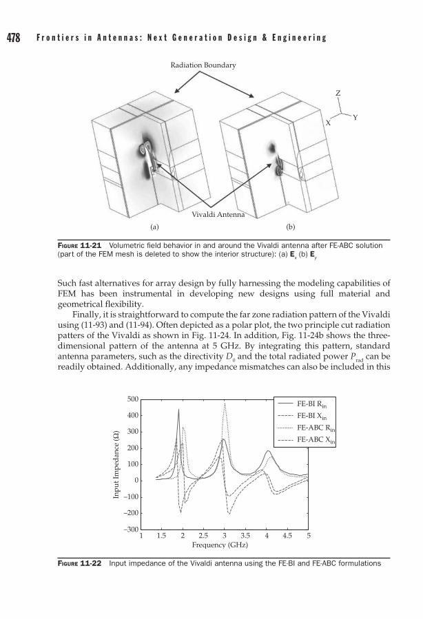
478 F r o n t i e r s i n a n t e n n a s : N e x t G e n e r a t i o n D e s i g n & e n g i n e e r i n g C h a p t e r 1 1 : N u m e r i c a l M e t h o d s i n a n t e n n a M o d e l i n g 479
Such fast alternatives for array design by fully harnessing the modeling capabilities of FEM has been instrumental in developing new designs using full material and geometrical flexibility.
Finally, it is straightforward to compute the far zone radiation pattern of the Vivaldi using (11-93) and (11-94). Often depicted as a polar plot, the two principle cut radiation patters of the Vivaldi as shown in Fig. 11-24. In addition, Fig. 11-24b shows the three-dimensional pattern of the antenna at 5 GHz. By integrating this pattern, standard antenna parameters, such as the directivity D0 and the total radiated power Prad can be readily obtained. Additionally, any impedance mismatches can also be included in this
Figure 11-21 Volumetric field behavior in and around the Vivaldi antenna after FE-ABC solution (part of the FEM mesh is deleted to show the interior structure): (a) E
x (b) E
y
(a) (b)
XY
Z
Vivaldi Antenna
Radiation Boundary
Figure 11-22 Input impedance of the Vivaldi antenna using the FE-BI and FE-ABC formulations
1 1.5 2 2.5 3 3.5 4 4.5 5–300
–200
–100
0
100
200
300
400
500
Frequency (GHz)
Inpu
t Im
ped
ance
(Ω)
FE-BI Rin
FE-BI Xin
FE-ABC Rin
FE-ABC Xin

478 F r o n t i e r s i n a n t e n n a s : N e x t G e n e r a t i o n D e s i g n & e n g i n e e r i n g C h a p t e r 1 1 : N u m e r i c a l M e t h o d s i n a n t e n n a M o d e l i n g 479
calculation to compute the overall antenna gains. In antenna design problems, the FEM systems needs to be solved for each frequency. For broadband antennas, this might be a time-consuming task. Instead, fast frequency sweep algorithms based on the asymptotic waveform evaluation (see [10] and references therein) can significantly speed up the broadband simulations. Moreover, large phased antenna arrays made of many identical antenna elements can be efficiently solved by exploiting the symmetries in the geometry. Several domain decomposition algo rithms have been developed [57], [51], [53] to efficiently tackle large FEM problems with geometrical repetitions. In the next section, we outline the domain decom position method in the FEM context.
Figure 11-23 A 49-element dual polarization Vivaldi array
X Y
Z
Figure 11-24 (a) Far-field patterns of the Vivaldi antenna at 5 GHz on the two principle cuts. (b) 3D rendering of the antenna patterns at 5 GHz.
2 4 6 8 10
30
6090
120
150
180 0
210
240270
300
330
(a) Far-Field Pattern
–10
0
10
20
–20–10
010
20
–20–10
010
20–20
(b) 3D Rendering

480 F r o n t i e r s i n a n t e n n a s : N e x t G e n e r a t i o n D e s i g n & e n g i n e e r i n g C h a p t e r 1 1 : N u m e r i c a l M e t h o d s i n a n t e n n a M o d e l i n g 481
11.3 Conformal Domain Decomposition MethodIn this section, we adopt the engineering notation, and employ j = −1.
11.3.1 NotationWe first introduce some notation and definitions that will be employed through out the manuscript. Boldface letters (e.g., u) are used to denote vectors in R3 while an overhead hat (e.g., u) will signify that the vector has unit magnitude. Finite dimensional matrices will be represented by uppercase italic characters (e.g., A), while lowercase italic characters will be used to represent column vec tors (e.g., x). The imaginary unit will be represented by j.
We will denote the time-harmonic electric and magnetic fields by E and H, respectively [58]. The free-space wavenumber will be denoted by k0 0 0= ω µ ε , where σ = 2π f is the radial frequency of operation and σ0 and µ0 are the permittivity and permeability in free space, respectively. The free-space intrinsic impedance is given byη µ ε0 0 0= / . In a material region, the wavenumber is given by k = ω µε , where σ and µ are the permittivity and permeability of the material. Also, we define σr = σ/σ0 and µr = µ /µ0 as the relative permittivity and permeability of the material.
In deriving the methods we will often consider a domain Ω R3 and its decomposition into Np = 2 subdomains such that Ω = Ω1 Ω2 (see Fig. 11-25). Further, we define the interface between subdomains as Γ := ∂Ω1 ∂Ω2, and the exterior boundaries as ∂Ωi := ∂Ωi ∂Ω. We denote the outward-directed unit normal to ∂Ωi by ni. The subscripts i 1, 2 will denote the restriction of a quantity to Ωi. For example, in Ωi, Ei will denote the electric field while σri and μri will denote the relative permittivity and permeability, respectively.
We will also use the tangential trace operator
γ τ ( ) : ˆ |u n ui i i i= × ∂Ω (11-95)
and tangential components trace operator
πτ ( ) : ˆ ( ˆ )|u n u ni i i i i= × × ∂Ω (11-96)
along with the associated jump and average operators on the interface Γ:
u u uγ τ τγ γ: ( ) ( )= +1 2 (11-97)
u u uπ τ τπ π: ( ) ( )= −1 2 (11-98)
u u uγ τ τγ γ: ( ( ) ( )).= −12 1 2
(11-99)
Figure 11-25 Notation for decomposition of the domain
n1n2
∼∂Ω1
∼∂Ω2∂Ω
Ω1Ω Ω2
Γ

480 F r o n t i e r s i n a n t e n n a s : N e x t G e n e r a t i o n D e s i g n & e n g i n e e r i n g C h a p t e r 1 1 : N u m e r i c a l M e t h o d s i n a n t e n n a M o d e l i n g 481
Volume and surface sesquilinear forms are defined by
( , ) :u v u vΩ Ω= ⋅∫ dv (11-100)
and
⟨ ⟩ = ⋅∂ ∂∫u v u v, : ,Ω Ωds (11-101)
where the overbar denotes conjugation. Note that we sometimes use (u, v)Ω to mean the broken form (u1, v1)Ω1 + (u2, v2)Ω2 and, similarly, ⟨u, v⟩∂Ω = ⟨ ⟩
∂Ωu v1 1,
1 + ⟨ ⟩
∂Ωu v2 2,
2.
We recall the standard Sobolev spaces Hs(Ω) for s ∈ R and Ht(∂Ω) for t ∈ [–1, 1] [59], and set
Hs sH( ) : ( ( ))Ω Ω= 3 (11-102)
Ht tH( ) : ( ( ))∂ = ∂Ω Ω 3 (11-103)
L H2 0( ) : ( )Ω Ω= (11-104)
L H2 0( ) : ( ).Ω Ω= (11-105)
Also, we define [60]
H u L u L( , ) : ( )| ( )curl Ω Ω Ω= ∇ ×∈ ∈2 2 (11-106)
H u L u( , ) : ( )| ( )div Ω Ω Ω= ∇ ⋅∈ ∈2 2L (11-107)
H u H u H− − −∂ = ∂ ∇ × ∂1 2 1 2 1 2/ / /( , ) : ( )| (curlτ τΩ Ω Ω∈ ∈ )), ˆ n u⋅ = 0 (11-108)
H u H u H− − −= ∂ ∇ ⋅ ∂1 2 1 2 1 2/ / /( , ) : ( )| ( )divτ τ∂Ω Ω Ω∈ ∈ ,, ˆ n u⋅ = 0 (11-109)
H u H u0 0( , ) : ( , )| ( ) .curl curl onΩ Ω Γ= =∈ γ τ D (11-110)
Note that H0(curl, Ω) is the space of curl-conforming functions that satisfy es sential boundary conditions on ΓD, the collection of surfaces on which Dirichlet boundary conditions are applied. This is the space in which the electric field resides, with the appropriate Dirichlet conditions imposed on Perfect Electri cally Conducting (PEC) surfaces. That is, we may write Ei ∈ H0(curl, Ωi). Similarly, the subscript 0 will be used with other function spaces to denote that essential Dirichlet boundary conditions are enforced.
Finally, we recall that the function spaces for the traces of curl-conforming functions are given via [60]
H u u H− ∂ =1 2/ ( , ) : ( )| ( , )curl curlτ τπΩ Ω∈ (11-111)
H u u H− ∂ =1 2/ ( , ) : ( )| ( , ),div curlτ τγΩ Ω∈ (11-112)

482 F r o n t i e r s i n a n t e n n a s : N e x t G e n e r a t i o n D e s i g n & e n g i n e e r i n g C h a p t e r 1 1 : N u m e r i c a l M e t h o d s i n a n t e n n a M o d e l i n g 483
and that
H H( , ) ( , )curl divΩ Ω′ = (11-113)
H H− −∂ ′ = ∂1 2 1 2/ /( , ) ( , )curl divτ τΩ Ω (11-114)
where X’ denotes the function space dual to X in the appropriate L2 inner product.
11.3.2 Interior Penalty Based Domain Decomposition MethodIn this section, we introduce a conformal DD method that does not require aux iliary variables to solve for time-harmonic Maxwell equations. The method is closely related to the Interior Penalty (IP) Discontinuous Galerkin (DG) meth ods of [61], [62]. A general derivation of the method leads to many possible formulations, but one that provides an optimal rate of convergence in solution error as well as robust iterative solver convergence is selected for further study.
When compared to the conventional FEM, the proposed method is less ac curate for a given mesh due to energy dissipation on interfaces. As with all computational methods, solution accuracy to a prescribed tolerance can only be guaranteed using adaptive procedures that either produce finer computational meshes (h-refine) or increase the polynomial order of basis functions (p-refine) based on reliable a posteriori error estimators. We note that adaptive mesh refinement is most efficient when the numerical method gives an optimal error convergence rate. The current work therefore addresses two of the three key ingredients for a robust numerical method by providing an efficient, reliable solution procedure and an optimal rate of convergence. The final ingredients, adaptive refinement procedures, are left to future research and the work in [63], in the context of DG methods, may provide a starting point.
11.3.2.1 Boundary Value ProblemWe begin by defining a Boundary Value Problem (BVP) for the decomposed problem of Fig. 11-25. It may be written as
∇ × ∇ × − = −−µ ε ηr rk jk11
1 02
1 1 0 0 1 1E E Jimp in Ω (11-115)
∇ × ∇ × − = −−µ ε ηr rk jk11
2 02
2 2 0 0 2 2E E Jimp in Ω (11-116)
π πτ τ( ) ( )E E1 2= on Γ (11-117)
γ µ γ µτ τr r11
1 21
2− −∇ ×( ) = ∇ ×E E( ) on Γ (11-118)
γ µ µ πτ τr rjk11
1 1 11
1 1− −∇ ×( ) = ∂E E( ) on Ω (11-119)
γ µ µ πτ τr rjk21
2 2 21
2 2− −∇ ×( ) = ∂E E( ) on Ω (11-120)
where Ei ∈ H0 (curl, Ωi) represents the electric field in a subdomain. Note that E1 and E2 are allowed to be discontinuous on Γ. Equations (11-117) and (11-118) enforce the

482 F r o n t i e r s i n a n t e n n a s : N e x t G e n e r a t i o n D e s i g n & e n g i n e e r i n g C h a p t e r 1 1 : N u m e r i c a l M e t h o d s i n a n t e n n a M o d e l i n g 483
necessary continuity of the electric and magnetic fields on the interface between subdomains and render the BVP above equivalent to that of the original problem without decomposition. Equations (11-119) and (11-120) provide a simple first-order absorbing boundary condition (ABC) on ∂ Ω, though other conditions may also be applied to the boundary. The impressed electric current is assumed to be given such that Ji
imp ∈ H(div, Ωi).We ignore other boundary conditions (e.g., PEC, PMC, and impedance conditions)
and sometimes omit discussion of the ABC treatment in what follows as they can be accounted for as in the conventional FEM.
11.3.2.2 Weak FormulationTo derive the weak form we first introduce the following residual quantities and their associated function spaces:
R E E J HΩ1
111
1 02
1 1 0 0 1( ) : (= ∇ × ∇ × − +−µ ε ηr rk jk imp d∈ iiv, )Ω1 (11-121)
R E E J HΩ2
221
2 02
2 2 0 0 2( ) : (= ∇ × ∇ × − +−µ ε ηr rk jk imp d∈ iiv, )Ω2
(11-122)
R E E HΓ Γ( ) /: ( ) ( ) ( , )31 2
1 2= − −π πτ τ τ∈ curl (11-123)
R E E HΓ( ) /: (4
11
1 21
21 2= ∇ ×( ) + ∇ ×( )− − −γ µ γ µτ τr r ∈ divvτ , )Γ (11-124)
R E E H∂
− − −= ∇ ×( ) −Ω1
511
1 1 11
11( ) /: ( )γ µ µ πτ τr rjk ∈ 22
1( )∂Ω (11-125)
R E E H∂
− − −= ∇ ×( ) −Ω2
621
2 2 21
21( ) /: ( )γ µ µ πτ τr rjk ∈ 22
2( ).∂Ω (11-126)
These residuals can be interpreted in terms of physical error currents that sup port a difference between the exact field solution and that obtained through the numerical method. RΩ1
(1) and RΩ2(2) represent scaled volume electric error currents, jk0σ0 JΩ1
err and jk0σ0 JΩ2
err, respectively. Also, surface error currents exist on the interface due to RΓ(3) and
RΓ(4). The former defines a rotated magnetic current, ni × MΓ
err, whereas the latter gives an electric current, JΓ
err.Following the Galerkin procedure we introduce test functions to form proper dual
pairs. These dual pairs can be interpreted via functional space arguments, or we may rely on a more physical interpretation using energy densities. These densities arise from dual pairs and we can then see that the volume electric currents, RΩ1
(i), should be paired with volume electric fields to give rise to the familiar E · J density. Thus, the test functions, wi are chosen from the same functional space as the electric field and we choose (w1, w2) ∈ H0(curl, Ω1) × H0(curl, Ω2). Similarly, we pair the rotated magnetic current of RΓ
(3) with a rotated magnetic field to give a surface energy density of the form H · M. Since the rotated magnetic field lies in the space H–1⁄2(divτ, Γ), we may use test functions of the form γτ(µri
–1∇ × wi). Lastly, the electric current of RΓ(4) is paired with a
surface electric field to give a surface density of the form E · J. The surface electric fields lie in the space H–1⁄2(curlτ, Γ) and we may use test functions πτ (wi).
484 F r o n t i e r s i n a n t e n n a s : N e x t G e n e r a t i o n D e s i g n & e n g i n e e r i n g C h a p t e r 1 1 : N u m e r i c a l M e t h o d s i n a n t e n n a M o d e l i n g 485
On Γ, two possibilities arise for the choice of basis functions, one from either side of the interface. Here, we simply choose an average of the two possibilities as testing functions. Now, we may write a linear combination of the weighted residuals
w R w R
w
11
22
3 11
1
11
22
, ,( ) ( )Ω Ω Ω Ω
( ) + ( )+ ∇ ×( )−c rγ µτ −− ∇ ×( ) + +−γ µ π πτ τ τr c2
12
34 1 2
4w R w w R, ( ) ( ),( ) (Γ Γ Γ
))
( )( ), ( ),
Γ
Ω Ω Ω+ +
∂ ∂ ∂ ∂c c5 1 4 2
6π πτ τw R w R1
12
(5)
ΩΩ
Γ Γ
2
+ − + ∇ ×( ) +−π π γ µ γ µτ τ τ τ( ) ( ), ( )w w R w1 23
11
1p r rr21
24 0− ∇ ×( ) =w R, ( )
Γ Γ
(11-127)
with coefficients c3, c4, c5, c6, p and q to be determined based on accuracy and convenience.
We note that the first four residuals are tested using the appropriate func tions to give proper dual pairings whereas the ABC residuals, R
∂Ω1
(5) and R∂Ω2
(6) , are tested with curl-conforming functions as in the conventional FEM.
The final two terms on the left-hand side of (11-127), inspired by the DG and IP methods (see, e.g., [61], [62], [64], [65]), are included to penalize the discontinuities of the electric and magnetic fields across Γ. We see their importance upon consider-ing the boundary testings
γ µτ r c q1
11 3
3 41 00− ∇ ×( ) + = ∀w R R w H, ( ,( ) ( )
Γ Γ Γ∈ curl ΩΩ
Γ Γ Γ
1
21
2 33 4
2 00
)
, (( ) ( )γ µτ r c q− ∇ ×( ) − = ∀w R R w H∈ cuurl, )Ω2
(11-128)
and
π
π
τ
τ
( ), ( , )
(
( ) ( )w R R w H
w
1 44 3
1 0 10c pΓ Γ ΓΩ+ = ∀ ∈ curl
22 44 3
2 0 20), ( , ).( ) ( )c pR R w HΓ Γ ΓΩ− = ∀ ∈ curl
(11-129)
The coefficients appearing in (11-128) and (11-129) can be chosen to weakly en force transmission conditions on the interface between subdomains and thereby satisfy (11-117) and (11-118). For a planar interface, the theory of non-overlapping DD methods for scalar and vector Helmholtz equations indicates that conver gent iterative methods (for propagative modes) may be obtained by enforcing a complex, mixed TC [66]–[68]. In the present work, evanescent modes are handled through the use of a Krylov subspace iterative solver, as is common in DD methods for wave phenomena [69]. Specifically, we choose c3 and c4 real, and set p = –jc4
%k/ %µr , q = jc3
%µr / %k with %k = (k1 + k2)/2 and %µr = ( %µ
r1 + %µr2)/2. Then, the TCs become the familiar ones of non-overlapping DD. Specifically
γ µ µ π γ µτ τ τr r rjk1
11
11 2
12
− − −∇ ×( ) − = − ∇ ×( )E E E% % ( ) −−
∇ ×( ) −
−
− −
jk
jk
r
r r
% %
% %
µ π
γ µ µ π
τ
τ τ
12
21
21
2
( )
(
E
E E )) ( ).= − ∇ ×( ) −− −γ µ µ πτ τr rjk11
11
1E E% % (11-130)
We denote the method that uses the Robin TC above as the IP-DD method.

484 F r o n t i e r s i n a n t e n n a s : N e x t G e n e r a t i o n D e s i g n & e n g i n e e r i n g C h a p t e r 1 1 : N u m e r i c a l M e t h o d s i n a n t e n n a M o d e l i n g 485
Now, after integrating the first two terms of (11-127) by parts, we obtain
∇ × ∇ ×( ) −
+ ∇ ×
−
−
w E w E
w
, ( , )
( ),
µ ε
π γ µτ τ
r r
r
k102
1 11
Ω Ω
EE w E1 2 21
2
3 11
1 2( ) + ∇ ×( )
+ ∇
∂−
∂
−
Ω Ωπ γ µ
γ µ
τ τ
τ
( ), r
rc ××( ) − ∇ ×( )+ +
−w w E
w w
1 21
2
4 1 22
γ µ
π π
τ π
τ τ
r
c
,
( ) ( )
Γ
,,
,
µ
µµ
γ
π π
r
rrjc
kjc
−
−
∇ ×
− + ∇ ×
1
4 31
E
w E
Γ
Γ
%ww E
w
%γ γ
τ τ
µµ
π γ µ
,
( ),
rr
r
k
c
− ∇ ×
+
1
5 1
Γ
111
1 1 11
1
6 2
1
− −∂
∇ ×( ) −
+
E E
w
jk
c
r
r
µ π
π γ µ
τ
τ τ
( )
( ),
Ω
221
2 2 21
2
0 0
2
− −∂
∇ ×( ) −
= −
E E
w J
jk
jk
rµ π
η
τ ( )
( ,
Ω
imp )) .Ω
(11-131)
Turning to the choice of constant coefficients, we first set c5 = c6 = –1 to enforce the ABCs on ∂Ω as in the usual FEM. Examining (11-131) and assum ing that the media are isotropic and μr is real, we can obtain a (convenient) symmetric formulation if c3 = –c4 = 1/2. Then, the weak formulation is given by
∇ × ∇ ×( ) −
+ ∇ ×
−
−
w E w E
w E
, ( , )
,
µ ε
µ γ
r r
r
k102
1
Ω Ω
ππ π γ
π π
µ
µ
Γ Γ
Γ
+ ∇ ×
+ +
−
%
%
w E
w E
,
,
r
r
j k j
1
2 2µµ
µµ
π
γ γ
τ
rr
rk
jk
− −∇ × ∇ ×
+
1 1
0
w E%
%,
(
Γ
ww E
w J
), ( )
( , ) .
µ ε π
η
τr r
jk
−∂
= −
1
0 0
Ω
Ωimp
(11-132)
We also note that many formulations can be derived by selecting different coeffi-cients in (11-130). However, it is as yet unclear how an effective precon-ditioner can be constructed for the resulting matrix. For example, with q = 0, the symmetric, nonsym-metric, and incomplete interior penalty methods can be obtained by setting c4 = 1
2 , 12 , or
0, respectively. The approximating properties of these methods have been analyzed in [61] and [62]. Note that some choices of coefficients may lead to suboptimal rates of con-vergence in the solution. We demonstrate via numerical experiment in Sections 11.3.4, that an optimal rate of convergence is obtained with the IP-DD method.
11.3.3 Discrete FormulationWhile the IP-DD method is applicable to both conformal and nonconformal meshes, we restrict ourselves here to the conformal case and introduce a partitioning, K, of Ω into a

486 F r o n t i e r s i n a n t e n n a s : N e x t G e n e r a t i o n D e s i g n & e n g i n e e r i n g C h a p t e r 1 1 : N u m e r i c a l M e t h o d s i n a n t e n n a M o d e l i n g 487
conformal mesh of tetrahedra, K. To form the subdomains Ω1 and Ω2, the mesh is partitioned by grouping whole tetrahedra to give submeshes K1 and K2. The surface meshes induced by the partitioning are denoted by Tx, with the subscript x referring to the original domain. For example, the triangulation on Γ is denoted by TΓ and that on ∂Ω is given by T∂Ω. On each of the subdomains, we define discrete trial and test functions, Ei
h ∈ Xih and wi
h ∈ Xih respectively, with Xi
h H0(curl, Ωi). Here, Xih is taken to be the space
of second-order, first kind Nedelec curl-conforming basis func tions [70] over Ki, given in [71]. We also set Eh := (E1
h, E2h), wh := (w1
h, w2h), and Xh := X1
h × X2h. The discrete problem
is then given by: Seek Eh ∈ Xh such that
a jkh h h h h( , ) ( , ) .w E w J w XK K= − ∀0 0η imp ∈ (11-133)
The sesquilinear form in (11-133) is given by
a kr r
r
( , ) : , ( , )
u v u v u vK K K= ∇ × ∇ ×( ) −
+ ∇
−
−
µ ε
µ
102
1 ×× + ∇ ×
+
−u v u u
u
, ,
,
γ π π γ
π
µ
µ
%
%
T Tr
j k
1
2 rrr
rr
j
k
%
%v u vπ γ
µµ
µT
+ ∇ × ∇ ×− −2
1 1,γγ
τ τπ µ ε π
T
T+ −
∂
jk r r01( ), ( ) .u v
Ω
(11-134)
After expanding the field in terms of the basis functions, the discrete system (11-133) can then be cast as a matrix equation for the electric field coefficients E1 and E2:
A CC A
EE
bb
1 12
21 2
1
2
1
2
=
(11-135)
where
AA A
A A D D T Sii i
i i ii ii ii ii
=+ + ( ) + + +
II IB
BI BB B B T B B RR
C CD D T
i
ij jiij ji ij
B
TB B T B
= =− − ( ) − +
( )0 0
0 SS
EEE
bbb
ij
ii
i
ii
i
B
I
B
I
B
=
=
.
(11-136)

486 F r o n t i e r s i n a n t e n n a s : N e x t G e n e r a t i o n D e s i g n & e n g i n e e r i n g C h a p t e r 1 1 : N u m e r i c a l M e t h o d s i n a n t e n n a M o d e l i n g 487
In (11-136), the superscripts x ∈ I, B correspond, respectively, to tetrahedra interior to the subdomain and those adjacent to its boundary, ∂Ωi. The block matrices are given by
A k
D
i i ri i i ri i
ij
i i
xx : , ( , )= ∇ × ∇ ×( ) −−w w w wµ ε102
K K
BB
B
: ( ),
: ( ),
= ∇ ×( )
=
−12
2
1π γ µ
π
τ τ
τ
w w
w
i rj j
ij iTj
TΓ
%%
%
%
%
k
Sj
k
rj
ij ri ir
µπ
γ µµ
γ
τ
τ τ
( )
: ,
w
w
TΓ
B = ∇ ×( )−2
1 µµ
π µ ε πτ τ
rj j
i i ri ri iR jk
−
−
∇ ×( )
=
1
01
w
w w
TΓ
B : ( ), ( )TT∂Ωi
.
(11-137)
We can solve (11-135) via a preconditioned Krylov subspace method. The simplest preconditioner is of block-Jacobi type and can be written as
MA
A=
1
2
00
. (11-138)
The system to be solved is of the form M–1Ax = M–1b and we see that applica tion of the preconditioner requires the inversion of each subdomain matrix, Ai. The subdomain matrices can be factorized in a preprocessing step or solved via another preconditioned Krylov method at each iteration (an “inner loop” iteration). Here, as a compromise between solution speed and memory usage, we use an incomplete factorization of each subdomain matrix to construct the preconditioner.
In addition to (11-138), other block preconditioners (e.g., Gauss-Seidel) may also be used. In serial these preconditioners entail a reasonable amount of additional computational effort; in parallel they may significantly increase com munication costs.
11.3.4 Numerical ResultsIn this section, we study the proposed method via numerical experiment. We restrict ourselves to the symmetric case with µr real and use a preconditioned Conjugate Residual (CR) solver [72] for the solution of (11-135). Note that despite the increased memory requirement, we prefer the CR algorithm to a Conjugate Gradient method because we have found that it provides more stable convergence. The convergence criteria for the CR solver is defined as
ε =−−
−
M Ax b
M b
12
12
( ). (11-139)
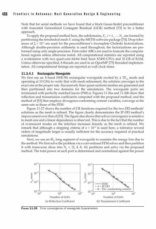
488 F r o n t i e r s i n a n t e n n a s : N e x t G e n e r a t i o n D e s i g n & e n g i n e e r i n g C h a p t e r 1 1 : N u m e r i c a l M e t h o d s i n a n t e n n a M o d e l i n g 489
Note that for serial methods we have found that a block Gauss-Seidel precon ditioner with truncated Generalized Conjugate Residual (GCR) method [73] to be a better approach.
To apply the proposed method here, the subdomains, Ki, i = 1, . . . , Np, are formed by partitioning the tetrahedral mesh K using the METIS software package [74]. Drop toler-ances of ξ = 10–6 are used for the preconditioner’s in complete Choleski factorizations. Although double-precision arithmetic is used throughout, the factorizations are per-formed using only single-precision. First-order ABCs are used to truncate the computa-tional regions unless otherwise noted. All computational statistics are reported using a workstation with two quad-core 64-bit Intel Xeon X5450 CPUs and 32 GB of RAM. Unless otherwise specified, 8 threads are used in an OpenMP [75] threaded implemen-tation. All computational timings are reported as wall clock times.
11.3.4.1 Rectangular WaveguideWe first use an X-band (WR-90) rectangular waveguide excited by a TE10 mode and operating at 10 GHz to verify that with mesh refinement, the solution converges to the exact one at the proper rate. Successively finer quasi-uniform meshes are generated and then partitioned into two domains for the simulations. The waveguide ports are terminated with perfectly matched layers (PMLs). Figures 11-26a and 11-26b show that reflection and transmission coefficients computed with the proposed method, and the method of [53] that employs divergence-conforming cement variables, converge at the same rate as those of the FEM.
Figure 11-27 shows the number of CR iterations required for the two DD methods’ solutions as the mesh is refined. The figure clearly demonstrates the IP-DD method’s improvement over that of [53]. The figure also shows that solver convergence is sensitive to mesh size and a linear dependence is observed. This is due to the fact that the number of evanescent modes on the interface increases linearly as the mesh is refined. We remark that although a stopping criteria of = 10–8 is used here, a tolerance several orders of magnitude larger is usually sufficient for the accuracy required of practical simulations.
Next, we use an 8λ0 long segment of waveguide to examine the energy loss due to the method. We first solve the problem via a conventional FEM solver and then partition it with transverse slices into Np ∈ 2, 4, 8, 16 partitions and solve via the proposed method. The total power at each port is determined and normalized against the power
Figure 11-26 Error convergence of waveguide S-parameters
(a) Reflection Coefficient
Number of DoFs Number of DoFs
(b) Transmission Coefficient
10–5
10–2
10–3
10–4
103 104 105 103 104 10510–2
10–2
10–4
10–4
FEMIP-DDDiv.-conforming cement
S 21
erro
r
S 11
erro
r

488 F r o n t i e r s i n a n t e n n a s : N e x t G e n e r a t i o n D e s i g n & e n g i n e e r i n g C h a p t e r 1 1 : N u m e r i c a l M e t h o d s i n a n t e n n a M o d e l i n g 489
obtained from the FEM solution. The experiment is repeated for several mesh sizes and the results are shown plotted in Fig. 11-28. We first note that the total power decreases linearly as the number of domains is increased. That is, each additional interface introduces a constant amount of loss. We also note that once again, as the mesh is refined, the solution converges toward the exact one at the optimal rate.
We note that in the present method, as with the conventional FEM and all numerical methods, no guarantee in solution accuracy is available unless (h or p) adaptive proce-dures are employed. No simple heuristic on mesh size is sufficient to guarantee a certain level of numerical accuracy. The important point for the method is that arbitrary solution accuracy can be obtained via mesh refinement or by increasing the polynomial order of the basis functions. If the method converges at the optimal rate, as shown above, the adaptive procedure is most efficient. Adaptive refinement for the present method will differ slightly from the conventional FEM in that additional refinement on subdomain
Figure 11-27 Solver convergence for waveguide with respect to mesh size, = 10–8
900
750
600
450
300
150
02 3 4 5 6 7 8 9 10
Elements per Wavelength
Iter
atio
ns
IP-DDDiv.-conforming cement
Figure 11-28 Energy loss in a waveguide with varying number of partitions and mesh size
1
0.98
0.96
0.940 4 8 12 16
Number of Partitions
Nor
mal
ized
Pow
er
4 elem/λ6 elem/λ8 elem/λ10 elem/λ

490 F r o n t i e r s i n a n t e n n a s : N e x t G e n e r a t i o n D e s i g n & e n g i n e e r i n g C h a p t e r 1 1 : N u m e r i c a l M e t h o d s i n a n t e n n a M o d e l i n g 491
interfaces may be desired. This local mesh refinement or polynomial enrichment on the interface would mitigate the energy dissipation since the order of the error is always on the same order of the error of the FEM method used within each subdomain.
11.3.4.2 Coated SphereWe further examine the accuracy of the proposed method using a plane-wave incident upon a dielectric-coated perfectly electrically conducting (PEC) sphere. The radii of the PEC sphere and the outer surface of the coating are r1 = 1λ0 and r2 = 1.2λ0, respectively. The coating has relative permittivity σr = 4 and the domain is truncated by a sphere of radius r3 = 3.2λ0. The bistatic radar cross-section (RCS) is found via a conventional FEM solver and the proposed method with Np ∈ 50, 100, 200 partitions. The error in RCS is determined using
RCS Errorref num
=−∫ | ( , ) ( , )| sinσ θ φ σ θ φ θ θ φ
π2
00d d
22
200
2
π
ππσ θ φ θ θ φ
∫
∫∫ | ( , )| sin,
ref d d (11-140)
where σnum is the numerical solution and σref is a reference solution obtained using the Mie series. Figure 11-29 shows that the solution of the proposed method once again converges at a rate equal to that of the FEM. Note that as the number of subdomains is increased, more error is introduced, as evidenced by the slight upward shift in the curves with increasing Np. This error is due to the loss of energy previously demonstrated in Section 11.3.4. The rates of convergence remain optimal and diminish as the solutions approach one where the error is dominated by the truncation error of the simple first order absorbing boundary condition. The bistatic RCS for mesh size h = λ0/6 is given in Fig. 11-30 and demonstrates good agreement with the Mie Series solution.
We now study the performance of the proposed method by comparing it to a p-type multiplicative Schwartz (pMUS) preconditioned FEM solver [76]. Here, only a single thread is used for a more fair comparison of the methods. It should be noted however,
Figure 11-29 RCS error for coated sphere with varying number of partitions and mesh size
10–1
100
1 2 3 4 5 6 7 8 9 10Elements per Wavelength
FEMNp = 50Np = 100Np = 200
RC
S E
rror

490 F r o n t i e r s i n a n t e n n a s : N e x t G e n e r a t i o n D e s i g n & e n g i n e e r i n g C h a p t e r 1 1 : N u m e r i c a l M e t h o d s i n a n t e n n a M o d e l i n g 491
that one of the IP-DD’s benefits is that it is an efficient parallel algorithm. We begin at an operating frequency of f = 50 MHz and use a coated sphere with r1 = 0.5λ0, r2 = 0.6λ0, r3 = 0.75λ0, and σr = 4. The domain is meshed with h = λ0/5 and solved via pMUS-FEM (that we denote by Np = 1) and the proposed method with Np ∈ 25, 50 partitions. The experiment is repeated for higher frequencies with the same computational domain and a new mesh such that h = λ0/5. A drop tolerance of σ = 10–3 is used for the factorizations of subdomain blocks.
The computational statistics are given in Table 11-2 where we see that for small problem geometries, the pMUS-FEM method is superior in terms of con vergence and solution time. Also, its memory requirements are reasonably low.
As the electrical size of the problem increases, we see that the pMUS precondi tioner is no longer effective and the solver fails to converge to = 10–3 within 1000 iterations. However, the proposed method is still able to obtain a solution.
The time and memory required for pMUS-FEM grow large due to the factor izations of large subblocks in the FEM matrix (that are obtained by splitting the hierarchical DoFs according to polynomial order). The time and memory required by the proposed method remains low due to the ability to control the size of the subblocks required for factorization; increasing Np leads to smaller subblocks for factorizations. Of course, the energy considerations discussed above and the effect on solution time must also be considered in determining the number of partitions to employ.
We now use the largest of the coated spheres to examine the parallel scalability of the method. We use Np = 50 subdomains and solve with 1 to 8 threads. The parallel speedup is measured as the total solution time required with t threads divided by the time required by the serial method. The results are shown in Fig. 11-31 and illustrate that a linear speedup is obtained when up to 4 threads are used. Beyond this, the
Figure 11-30 Bistatic RCS for coated sphere with varying number of partitions, h = λ0/6, σ = 0
0
–5
–10
–15
–20
–25
0
–1
–2
0
–1
–20 5 10 0 5 10
–30
Mie seriesFEMNp = 50Np = 100Np = 200
–35
–400 45 90 135 180
θ (deg.)
Bis
tati
c R
CS
(dB
)

492 F r o n t i e r s i n a n t e n n a s : N e x t G e n e r a t i o n D e s i g n & e n g i n e e r i n g C h a p t e r 1 1 : N u m e r i c a l M e t h o d s i n a n t e n n a M o d e l i n g 493
Table 11-2 Computational Statistics for Coated Sphere Simulations
Np
Frequency (MHz)
Degrees of Freedom
Iterations ( = 10–3)
Preconditioner Time (s)
Solution Time (s)
Peak Memory Usage (MB)
1 50 11,382 6 1 0.3 26
100 77,868 54 20 18 190
150 256,196 40 213 53 699
200 612,726 a 974 — 1792
250 1,067,078 — 2670 — 3553
300 1,875,096 — 9215 — 7692
25 50 15,016 49 0.5 1.4 8
100 90,088 118 19 31 20
150 284,204 161 225 179 74
200 662,938 185 1210 593 213
250 1,136,124 170 3752 1095 434
300 1,978,766 240 11923 3190 870
50 50 17,154 72 0.3 2.3 8
100 95,624 146 11 35 20
150 296,066 135 118 135 52
200 684,042 239 659 677 118
250 1,166,672 188 2110 1082 202
300 2,024,852 352 5833 4040 402
aFailed to converge within 1000 CR iterations
Figure 11-31 Parallel speedup for a coated sphere
6
4
2
6
4
21 2 3 4 5 6 7 8
Number of Processors
Spee
dup
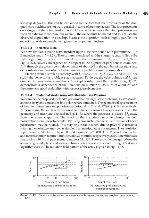
492 F r o n t i e r s i n a n t e n n a s : N e x t G e n e r a t i o n D e s i g n & e n g i n e e r i n g C h a p t e r 1 1 : N u m e r i c a l M e t h o d s i n a n t e n n a M o d e l i n g 493
speedup degrades. This can be explained by the fact that the processors of the dual quad-core machine are not truly parallel in terms of memory access. The four processors on a single die share two banks of 6 MB L2 cache. When more than two processors are used on a die (or more than four overall), the cache must be shared and this causes the observed degradation in speedup. Because the algorithm itself is highly parallel, we expect it to scale extremely well given the proper architecture.
11.3.4.3 Dielectric CubeWe now simulate a plane-wave incident upon a dielectric cube with permittivity σr = 2 and edge length l1 = 1.2λ0. The scatterer is enclosed within a larger vacuum-filled cube with edge length l2 = 2λ0. The model is meshed quasi-uniformly with h = λ0/6. In Fig. 11-32a, solver convergence with respect to the number of partitions is examined. A fit through the data shows a dependence of about Np
18 in the number of iterations and
demonstrates an insensitivity to the number of partitions used in simulation.Starting from a similar geometry with l1 = 0.6λ0, l2 = 1λ0, h = λ0/6, and Np = 4, we
study the behavior as problem size increases. To do so, the cube volume and Np are doubled for successive simulations. h is kept constant and the results of Fig. 11-32b demonstrate a dependence of the iterations on number of DoFs, N, of about N
17 and
therefore very good scalability with respect to problem size.
11.3.4.4 Conformal Vivaldi Array with Meander-Line PolarizerTo examine the proposed method’s performance on large-scale problems, a 7 × 7 Vivaldi antenna array and a meander-line polarizer are simulated. The geomet rical specifications of the antenna elements and polarizer can be found in [51] and [77] (App. C.8), respectively. After meshing, the mesh is transformed so as to be conformal to a spherical surface. The geometry and mesh are depicted in Fig. 11-33 where the polarizer is placed 2
3 0λ away from the antenna aperture. The effect of the meander-lines is to change the field polarization from linear to circular. By using two such polarizers, the direction of linear polarization may be rotated. This may be desirable when, due to physical constraints, rotating the polarizers may be far simpler than manipulating the antenna. The simulation is performed at 5 GHz with Np = 1000 and requires 10,275,060 DoFs. Preconditioner setup and matrix solution require 4 minutes, and 22 minutes, respectively. 226 CR iterations are required ( = 10–2) and peak memory usage is 22.4 GB. The electric field magnitude on the antenna, ground plane and exterior truncation surface are shown in Fig. 11-34 on a logarithmic scale. The radiation field pattern of the array is given in Fig. 11-35.
Figure 11-32 Dielectric cube solver convergence with respect to varying problem parameters, = 10–8
(a) Increasing number of partitions (b) Increasing problem size andnumber of partitions
103
102
100 101 102 103 104 104 105 106 107
Number of Partitions
11
7
8
Number of DoFs
Iter
atio
ns
103
102
Iter
atio
ns
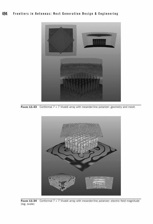
494 F r o n t i e r s i n a n t e n n a s : N e x t G e n e r a t i o n D e s i g n & e n g i n e e r i n g C h a p t e r 1 1 : N u m e r i c a l M e t h o d s i n a n t e n n a M o d e l i n g 495
Figure 11-33 Conformal 7 × 7 Vivaldi array with meander-line polarizer: ge ometry and mesh
Figure 11-34 Conformal 7 × 7 Vivaldi array with meander-line polarizer: electric field magnitude (log. scale)

494 F r o n t i e r s i n a n t e n n a s : N e x t G e n e r a t i o n D e s i g n & e n g i n e e r i n g C h a p t e r 1 1 : N u m e r i c a l M e t h o d s i n a n t e n n a M o d e l i n g 495
11.3.4.5 Dipole Array in an Aircraft RadomeNext, a circular array of 137 quarter-wavelength dipoles operating at f = 5 GHz is simulated in the presence of a conical dielectric aircraft radome with σr = 3. The array and radome are shown in Fig. 11-36a along with a shape-conforming truncation surface 13 0λ away from the radome’s exterior. The radome has length 14.7λ0, outer diameter 7λ0,
Figure 11-35 Radiation pattern of a conformal 7 × 7 Vivaldi array with meander-line polarizer
0
–10
–20
–30
–40–90 –60 –30 0 30 60 90
θ (deg.)
Tota
l Fie
ld (d
B)
φ = 0
φ = 90
Figure 11-36 Aircraft radome with circular dipole array
(a) Geometry, l = 14.7 λ0, d = 7 λ0
(b) Mesh Partition (c) Electric Field Magnitude
d
l

496 F r o n t i e r s i n a n t e n n a s : N e x t G e n e r a t i o n D e s i g n & e n g i n e e r i n g C h a p t e r 1 1 : N u m e r i c a l M e t h o d s i n a n t e n n a M o d e l i n g 497
and thickness 16 0λ , The mesh of 1,993,853 tetrahedra is partitioned into 500 domains
(shown in Fig. 11-36b) and results in 14,370,776 DoFs. Preconditioner setup requires 32 minutes, while 21 minutes are required for 82 CR iterations ( = 10–2). Peak memory usage is 24.5 GB. The magnitude of the electric field on the radome is shown in Fig. 11-36c. Figures 11-37 and 11-38 show, respectively, the radiation field patterns of the dipole array alone and in the presence of the radome. The effect of the radome on the copolarization is apparent in the increased level of the sidelobes, with the first one increasing from –28 to –12 dB relative to the main lobe. Signif icant cross-polarization is also introduced, with the peak value increasing from –55 to –19 dB.
11.3.4.6 Horn Antenna Array Fed by a Rotman LensThe next electrically large simulation is that of a horn antenna array fed by a Rotman lens. The goal of the lens is to provide linear phase to an antenna array such that the radiated power can be guided in a particular direction. The geometry is depicted in Fig. 11-39. The lens has width 12λ0 and length 10.4λ0 at the operating frequency in the upper C to lower X band. The lens is filled with a dielectric of permittivity σr = 2.5 – j0.00475. Sixteen input ports and and 32 output ports are connected to microstrip transmission lines via SMA connectors as shown in the center inset of Fig. 11-39. The output ports are then connected via coaxial cables of equal length to 32 horn antenna elements. The horn elements have a small transition from coaxial cable to the wave
Figure 11-38 Radiation patterns of a circular dipole array with aircraft radome
(a) Co polarization (b) Cross-polarization
–100
0–25
–50
–75–100
60 300
–30–60 –60 –30 0
θ (deg.)φ (deg.)
6030
0–30
–60φ (deg.)
Tota
l Fie
ld (d
B) 0
–25
–50
–75–100To
tal F
ield
(dB
)
30 60
–60–30 0
θ (deg.)
3060
–75 –50 –25 0 –100 –75 –50 –25 0
Figure 11-37 Radiation patterns of a circular dipole array
(a) Copolarization (b) Cross-polarization
–100
0
–25
–50
–75–100
6030
0–30
–60 –60 –30 0
θ (deg.)φ (deg.)
6030
0–30
–60φ (deg.)
Tota
l Fie
ld (d
B) 0
–25
–50
–75–100To
tal F
ield
(dB
)
30 60
–60 –30 0
θ (deg.)
3060
–75 –50 –25 0 –100 –75 –50 –25 0

496 F r o n t i e r s i n a n t e n n a s : N e x t G e n e r a t i o n D e s i g n & e n g i n e e r i n g C h a p t e r 1 1 : N u m e r i c a l M e t h o d s i n a n t e n n a M o d e l i n g 497
guiding structure (upper inset of Fig. 11-39). Each horn element is 6.6λ0 high and 2λ0 × 0.36λ0 at the aperture. The entire geometry is enclosed in an L-shaped box with its boundary never less than 1
3 0λ from the geometry.Simulations are performed for two input port excitations with the first ex citation
toward the center of the lens and the second one off-center. The excitation port determines the amount of phase variation in the output ports: the further the excitation port from center, the larger the phase variation and beamsteering angle.
The mesh consists of 2,847,778 tetrahedra and a decomposition into 1000 domains leads to 18,190,650 DoFs. The preconditioner setup requires 12 min utes and must be performed only once for both port excitations. The center port simulation requires 42 minutes for 281 CR iterations ( = 10–2), whereas the off-center excitation requires 48 minutes for 313 iterations. Both simulations have peak memory usages of 30.7 GB.
The electric field magnitudes, plotted with logarithmic scales, are given in Figs. 11-40a and 11-40b and the radiation patterns in Fig. 11-41. The effect of varying the excited input port is clearly visible upon examination of the wavefronts in Figs. 11-40a and 11-40b. Note that in the case of the “center” port excitation, a small phase difference occurs at the output ports due to the fact that the even number of input ports requires a slightly off-center input. A much larger phase variation is seen for the off-center input. The fields on the apertures of the horn antennas confirm this as do the radiation patterns that show main lobes centered at 3.5 and 39.5 degrees, for center and off-center excitations, respectively.
Figure 11-39 Configuration of the Rotman lens and horn antenna array. Insets (from upper right, clockwise): coax-to-horn antenna transitions, SMA connec tors, and mesh decomposition.

498 F r o n t i e r s i n a n t e n n a s : N e x t G e n e r a t i o n D e s i g n & e n g i n e e r i n g C h a p t e r 1 1 : N u m e r i c a l M e t h o d s i n a n t e n n a M o d e l i n g 499
Figure 11-41 Radiation patterns of a Rotman lens feeding a horn antenna array
(a) Center port excitation (b) Off-center port excitation
0
–10
–20
–30
–40–90 –60 –30 0 30 60 90
θ (deg.)
φ = 0φ = 90
φ = 0φ = 90
–90 –60 –30 0 30 60 90θ (deg.)
Tota
l Fie
ld (d
B)
0
–10
–20
–30
–40
Tota
l Fie
ld (d
B)
11.3.4.7 F-16 ScatteringFinally, we simulate the scattering of a f = 1 GHz plane-wave incident upon a long-range F-16 jet. The problem geometry, with a truncation boundary at least λ0/3 away from the scatterer, is approximately 15 m long, 8 m wide, and 4.5 m high. A hollow dielectric radome with permittivity σ = 3 is placed at the front of the aircraft while a glass canopy with σ = 4.7 – j0.0705 sits atop the PEC body to form the cockpit. Figure 11-42 shows the geometry of the jet along with the surface mesh and the inset illustrates the partitioning of the 2,8444,939 tetrahedra into 500 domains. In this case, simulation of the 19,817,336 DoF problem could not be fit entirely into RAM, and the factorizations were written and read from disk only when necessary. This considerably increases the wall clock time and, because the disk operations are performed serially, seriously impacts parallel efficiency. In light of this, we employ a serial Gauss-Seidel preconditioner with a truncated GCR(5) solver for this simulation, though the matrix vector multiplication is still performed in parallel.
Figure 11-40 (a) Electric field (log. scale) of a Rotman lens feeding a horn antenna array, center port excitation. (b) Electric field (log. scale) of a Rotman lens feeding a horn antenna array, off-center port excitation.
(a) (b)

498 F r o n t i e r s i n a n t e n n a s : N e x t G e n e r a t i o n D e s i g n & e n g i n e e r i n g C h a p t e r 1 1 : N u m e r i c a l M e t h o d s i n a n t e n n a M o d e l i n g 499
Figure 11-42 F-16 geometry and surface mesh. Inset: mesh decomposition
The simulations of both nose-on and oblique incidence required 1 hour and 52 minutes for preconditioner setup and a peak memory of 19.23 GB. The nose-on simulation required 4 hours and 50 minutes for 39 iterations while the oblique simulation used 4 hours and 10 minutes for 36 iterations. The electric fields on the F-16 are depicted in Figs. 11-43a and 11-43b for the nose-on and oblique excitations.
Figure 11-43 (a) Electric field of F-16 scattering problem, normally incident excitation. (b) Electric field of F-16 scattering problem, obliquely incident excitation.
(a) (b)

500 F r o n t i e r s i n a n t e n n a s : N e x t G e n e r a t i o n D e s i g n & e n g i n e e r i n g C h a p t e r 1 1 : N u m e r i c a l M e t h o d s i n a n t e n n a M o d e l i n g 501
ReferencesF. L. Teixeira, “Time-domain finite-difference and finite-element methods for Maxwell equations [1] in complex media,” IEEE Trans. Antennas Propagat., vol. 56, no. 8, pp. 2151–2166, 2008.F. L. Teixeira, and W. C. Chew, “Finite-difference computation of transient electromagnetic fields for [2] cylindrical geometries in complex media,” IEEE Trans. Geosci. Remote Sens., vol. 38, no. 4, pp.1530–1543, 2000.B. Donderici, and F. L. Teixeira, “Conformal perfectly matched layer for the mixed finite element [3] time-domain method,” IEEE Trans. Antennas Propagat., vol. 56, no. 4, pp. 1017–1026, 2008.N. Venkatarayalu, C.-C. Chen, F. L. Teixeira, and R. Lee, “Numerical mod eling of ultra-wideband [4] dielectric horn antennas using FDTD,” IEEE Trans. Antennas Propagat., vol. 52, no. 5, pp. 1318– 1323, 2004.K.-H. Lee, C.-C. Chen, F. L. Teixeira, and R. Lee, “Modeling and charac terization of geometrically [5] complex UWB antennas using FDTD,” IEEE Trans. Antennas Propagat., vol. 52, no. 8, pp. 1983– 1991, 2004.K.-Y. Jung, and F. L. Teixeira, “Photonic crystals with a degenerate band edge: Field enhancement [6] effects and sensitivity analysis,” Phys. Rev. B, vol. 77, no. 12, 2008.K.-Y. Jung, F. L. Teixeira, and R. Reano, “Au SiO2 nanoring plasmon waveguides at optical com-[7] munication band,” J. Lightwave Technol., vol. 25, no. 9, pp. 2757–2765, 2007.A. Taflove, and S. Hagness, “[8] Computational Electrodynamics: The Finite-Difference Time-Domain Method,” Artech House, Norwood, MA, 2005.J.-F. Lee, R. Lee, and A. C. Cangellaris, “Time domain finite element methods,” [9] IEEE Trans. Antennas Propagat., vol. 45, no. 3, pp. 430–442, 1997.J. M. Jin, [10] The Finite Element Method in Electromagnetics, 2nd ed. John Wiley, New York, 2002.S. Wang, and F. L. Teixeira, “Some remarks on the stability of time-domain electromagnetic simula-[11] tions,” IEEE Trans. Antennas Propagat., vol. 52, no. 3, pp. 895–898, 2004.B. Donderici, and F. L. Teixeira, “Mixed finite-element time-domain method for Maxwell equations [12] in doubly-dispersive media,” IEEE Trans. Microwave Theory Tech., vol. 56, no. 1, pp. 113–120, 2008.H. O. Lee, and F. L. Teixeira, “Cylindrical [13] FDTD analysis of LWD tools through anisotropic dipping-layered earth media,” IEEE Trans. Geosci. Remote Sens., vol. 45, no. 2, pp. 383–388, 2007.C. Kung, and R. Lee, “Alternative [14] FDTD updating schemes for anisotropic materials,” IEEE Trans. Antennas Propagat., vol. 57, no. 12, pp. 895–898, 2009.J. P. Berenger, “A perfectly matched layer for the absorption of electromag netic waves,” [15] J. Comput. Phys., vol. 114, no. 2, pp. 185–200, 1994.F. L. Teixeira, and W. C. Chew, “Complex space approach to perfectly matched layers: A review [16] and some new developments,” Int. J. Numer. Model., vol. 13, pp. 441–455, 2000.J. A. Roden, and S. D. Gedney, “Efficient implementation of the uniaxial-based PML media in [17] three-dimensional nonorthogonal coordinates with the use of the FDTD technique,” Microw. Opt. Technol. Lett., vol. 14, no. 2, pp. 71–75, 1997.M. Kuzuoglu, and R. Mittra, “Investigation of nonplanar perfectly matched absorbers for finite-[18] element mesh truncation,” IEEE Trans. Antennas Prop agat., vol. 45, no. 3, Mar. 1997.F. L. Teixeira, and W. C. Chew, “Analytical derivation of a conformal per fectly matched absorber [19] for electromagnetic waves,” Microw. Opt. Tech. Lett., vol. 17, no. 4, pp. 231–236, 1998.F. L. Teixeira, W. C. Chew, M. Straka, M. L. Oristaglio, and T. Wang, “Finite-difference time-domain [20] simulation of ground penetrating radar on dispersive, inhomogeneous, and conductive soils,” IEEE Trans. Geosci. Re mote Sens., vol. 36, no. 6, pp. 1928–1937, June 1998.B. He, and F. L. Teixeira, “On the degrees of freedom of lattice electrody namics,” [21] Phys. Lett. A, vol. 336, pp. 1–7, 2005.F. C. Yang, and K. S. H. Lee, “Impedance of a two-conical-plate transmission line,” [22] Sensor and Simulation Notes, Air Force Research Laboratory, Nov. 1976.J. L. Volakis, A. Chatterjee, and L. Kempel, [23] Finite Element Methods for Electromagnetics. New York: IEEE Press, 1998.J. Jin, and D. J. Riley, [24] Finite Element Analysis of Antennas and Arrays. Wiley-IEEE Press, 2008.P. P. Silvester, and G. Pelosi, [25] Finite elements for wave electromagnetics. New York: IEEE Press, 1994.Y. Zhu, and A. Cangellaris, [26] Multigrid Finite Element Methods for Electromangtic Field Modeling. New Jersey: IEEE Press, 2006.P. Monk, [27] Finite Element Methods for Maxwell’s Equations. Clarendon Press, Oxford, 2003.A. Bossavit, [28] Computational Electromagnetism. Academic Press, San Diego, 1998.J. C. Nedelec, “Mixed finite elements in r3,” [29] Numerische Mathematik, vol. 35, pp. 315–341, 1980.P. G. Ciarlet, [30] The Finite Element method for Elliptic Problems, Volume 4 of Studies in Mathematics and Its Applications, North-Hollan, New York, 1978.

500 F r o n t i e r s i n a n t e n n a s : N e x t G e n e r a t i o n D e s i g n & e n g i n e e r i n g C h a p t e r 1 1 : N u m e r i c a l M e t h o d s i n a n t e n n a M o d e l i n g 501
R. D. Graglia, “The use of parametric elements in the moment method solution of static and dynamic [31] volume integral equations,” IEEE Trans. Antennas and Propagation, vol. 36, no. 5, pp. 636–646, May 1988.M. I. Sancer, R. L. McClary, and K. J. Glover, “Electromagnetic computa tion using parametric [32] geometry,” Electromagnetics, vol. 10, pp. 85–103, 1990.G. E. Antilla, and N. G. Alexopoulos, “Scattering from complex 3d geome tries by a curvilinear [33] hybrid finite element-integral equation approach,” J. Opt. Soc. Am. A., vol. 11, no. 4, pp. 1445– 1457, 1994.T. Ozdemir, and J. L. Volakis, “Triangular prisms for edge-based vector finite elements analysis of [34] conformal antennas,” IEEE Trans. Antennas Propagat., vol. 45, no. 5, pp. 788–797, May 1997.Z. J. Cendes, “Vector finite elements for electromagnetic field computation,” [35] IEEE Trans Magnatics, vol. 27, no. 5, pp. 3958–3966, Sept. 1991.B. Engquist, and A. Majda, “Absorbing boundary conditions for the numer ical simulation of [36] waves,” Math. Comput., vol. 31, pp. 629–651, 1977.A. Bayliss, and E. Turkel, “Radiation boundary conditions for wave-like equations,” [37] Appl. Math., vol. 33, pp. 707–725, 1980.Stratton, J. A., [38] Electromagnetic Theory. Wiley-Interscience, Classic Reis sue, 2007.X. Q. Sheng, J.-M. Jin, J. M. Song, C. C. Lu, and W. C. Chew, “On the formulation of hybrid finite-[39] element and boundary-integral methods for 3d scattering,” IEEE Trans. Antennas Propagat., vol. 46, no. 3, pp. 303–311, Mar. 1998.T. F. Eibert, J. L. Volakis, D. R. Wilton, and D. R. Jackson, “Hybrid febi modeling of 3d doubly [40] periodic structures utilizing triangular prismatic elements and a mpie formulation accelerated by the ewald transformation,” IEEE Trans. Antennas Propagat., vol. 47, no. 5, pp. 843–850, Mar. 1999.M. Vouvakis, S. C. Lee, K. Zhao, and J. F. Lee, “A symmetric fem-ie formula tion with a single-[41] level ie-qr algorithm for solving electromagnetic radiation and scattering problems,” IEEE Trans. Antennas Propagat., vol. 52, pp. 3060–3070, Nov. 2004.M. M. Botha, and J.-M. Jin, “On the variational formulation of hybrid finite element-boundary [42] integral techniques for electromagnetic analysis,” IEEE Trans. Antennas Propag., vol. 52, no. 11, pp. 3037–3047, Nov. 2004.R. D. Graglia, D. R. Wilton, and A. F. Peterson, “Higher order interpolatory vector bases for [43] computational electromagnetics,” IEEE Trans. Antennas Propagat., vol. 45, no. 3, pp. 329–342, March 1997.R. D. Graglia, D. R. Wilton, A. F. Peterson, and I.-L. Gheorma, “Higher order interpolatory vector [44] bases on prism elements,” IEEE Trans. Antennas Propagat., vol. 46, no. 3, pp. 442–450, Mar. 1998.J. P. Webb, “Hierarchical vector basis functions of arbitrary order for tri angular and tetrahedral [45] finite elements,” IEEE Trans. Antennas Propag., vol. 47, no. 8, pp. 1244–1253, Aug. 1999.L. S. Andersen, and J. L. Volakis, “Development and application of a novel class of hierarchical [46] tangential vector finite elements for electromagnetics,” IEEE Trans. Antennas Propagat., vol. 47, no. 1, pp. 112–120, Jan. 1999.E. Jorgensen, J. L. Volakis, P. Meincke, and O. Breinbjerg, “Higher order hierarchical legendre [47] basis functions for electromagnetic modeling,” IEEE Trans. on Antennas and Propagation, pp. 2985– 2995, 2004.D. K. Sun, Z. Cendes, and J.-F. Lee, “Adaptive mesh refinement, h-version, for solving multi-[48] port microwave devices in three dimensions,” IEEE Trans. Magn., vol. 36, no. 4, pp 1596–1599, Jul. 2000.T. B. A. Senior, and J. L. Volakis, [49] Approximate Boundary Conditions in Electromagnetics. IET Press, 1995.Y. Zhang, R. A. van de Geijin, M. C. Taylor, and T.K. Sarkar, “Parallel mom using hihger-order [50] basis functions and plapack in-core and out-of-core solvers for challenging em simulations,” IEEE Antennas Propagation Magazine, vol. 51, no. 5, pp. 42–60, Oct. 2009.S.-C. Lee, M. N. Vouvakis, and J.-F. Lee, “A non-overlapping domain decom position method with [51] non-matching grids for modeling large finite antenna arrays,” J. Comput. Phys., vol. 203, no. 1, pp. 1–21, 2005.M. N. Vouvakis, Z. Cendes, and J.-F. Lee, “A FEM domain decomposition method for photonic [52] and electromagnetic band gap structures,” IEEE Trans. Antennas and Propagation, vol. 54, no. 2, pp. 721–733, Feb. 2006.K. Zhao, V. Rawat, S.-C. Lee, and J.-F. Lee, “A domain decomposition method with nonconformal [53] meshes for finite periodic and semi-periodic structures,” IEEE Trans. Antennas and Propagation, vol. 55, no. 9, pp. 2559–2570, Sept. 2007.Z. Peng, V. Rawat, and J.-F. Lee, “One way domain decomposition method with second order [54] transmission conditions for solving electromagnetic wave problems,” J. Comput. Phys., vol. 229, no. 4, pp. 1181–1197, 2010.

502 F r o n t i e r s i n a n t e n n a s : N e x t G e n e r a t i o n D e s i g n & e n g i n e e r i n g
R. Coifman, V. Rokhlin, and S. Wandzura, “The fast multipole method for the wave equation: [55] A pedestrian prescription,” IEEE Antenna Propagat. Magazine, vol. 35, no. 3, pp. 7–12, June 1993.E. Bleszynski, M. Bleszynski, and T. Jaroszewicz, “Aim: Adaptive inte gral method for solving large-[56] scale electromagnetic scattering and radiation problems,” Radio Sci., vol. 31, no. 5, pp. 1225–1251, Sep./Oct. 1996.R. W. Kindt, K. Sertel, E. Topsakal, and J. L. Volakis, “Array decomposition method for the accu-[57] rate analysis of finite arrays,” IEEE Trans. Antennas and Propagation, vol. 51, no. 6, pp. 1364–1372, June 2003.R. Harrington, [58] Time-Harmonic Electromagnetic Fields. John Wiley & Sons, New York, 2001.R. A. Adams, [59] Sobolev spaces. Academic Press, New York-London, 1975. Pure and Applied Mathematics, vol. 65.P. Monk, [60] Finite Element Methods for Maxwell’s Equations. Numerical Mathematics and Scientific Computation. Oxford University Press, New York, 2003.P. Houston, I. Perugia, A. Schneebeli, and D. Schotzau, “Interior penalty method for the indefinite [61] time-harmonic Maxwell equations,” Numer. Math., vol. 100, no. 3, pp. 485–518, 2005.A. Buffa, P. Houston, and I. Perugia, “Discontinuous Galerkin computation of the Maxwell eigen-[62] values on simplicial meshes,” J. Comput. Appl. Math., vol. 204, no. 2, pp. 317–333, 2007.P. Houston, I. Perugia, and D. Schotzau, “Energy norm a posteriori error estimation for mixed [63] discontinuous Galerkin approximations of the Maxwell operator,” Comput. Methods Appl. Mech. Engrg., vol. 194, no. (2–5), pp. 499–510, 2005.D. N. Arnold, “An interior penalty finite element method with discontinuous elements,” [64] SIAM J. Numer. Anal., vol. 19, no. 4, pp. 742–760, 1982.D. N. Arnold, F. Brezzi, B. Cockburn, and L. D. Marini, “Unified analysis of Discontinuous Galerkin [65] methods for elliptic problems,” SIAM J. Numer. Anal., vol. 39, no. 5, pp. 1749–1779, 2002.B. Despres, [66] Methodes de décomposition de domaine pour les problémes de propagation d’ondes en régime harmonique. PhD thesis, Université Dauphine–Paris IX, 1991.B. Després, P. Joly, and J. E. Roberts, “A domain decomposition method for the harmonic Maxwell [67] equations,” In Iterative methods in linear algebra (Brussels, 1991), pp. 475–484. North-Holland, Amsterdam, 1992.M. N. Vouvakis, [68] A Non-Conformal Domain Decomposition Method for Solving Large Electromagnetic Wave Problems. PhD thesis, Ohio State University, Columbus, Ohio, 2005.K. Zhao, [69] A Domain Decomposition Method for Solving Electrically Large Electromagnetic Problems. PhD thesis, Ohio State University, Colum bus, Ohio, 2007.J.-C. Nédélec, “Mixed finite elements in [70] R3,” Numer. Math., vol. 35, no. 3, pp. 315–341, 1980.D.-K. Sun, J.-F. Lee, and Z. Cendes, “Construction of nearly orthogonal Nedelec bases for rapid [71] convergence with multilevel preconditioned solvers,” SIAM Journal on Scientific Computing, vol. 23, no. 4, pp. 1053–1076, 2001.D. G. Luenberger, “The conjugate residual method for constrained mini mization problems,” [72] SIAM Journal on Numerical Analysis, vol. 7, no. 3, pp. 390–398, 1970.S. C. Eisenstat, H. C. Elman, and M. H. Schultz, “Variational iterative meth ods for nonsymmetric [73] systems of linear equations,” SIAM Journal on Nu merical Analysis, vol. 20, no. 2, pp. 345–357, 1983.G. Karypis, and V. Kumar, “A fast and high quality multilevel scheme for partitioning irregular [74] graphs,” SIAM J. Sci. Comput., vol. 20, no. 1, pp. 359–392 (electronic), 1998.B. Chapman, G. Jost, and R. van der Pas, [75] Using OpenMP: Portable Shared Memory Parallel Programming. MIT Press, Cambridge, Mas sachusetts, 2008.J.-F. Lee, and D.-K. Sun, “[76] p-Type multiplicative Schwarz (pMUS) method with vector finite ele-ments for modeling three-dimensional waveguide dis continuities,” IEEE Trans. Microwave Theory and Techniques, vol. 52, no. 3, pp. 864–870, 2004.B. A. Munk, [77] Finite Antenna Arrays and FSS. John Wiley & Sons, New York, 2003.

AABC (absorbing boundary condition)
computation of antenna radiation properties, 475
computation of FEM matrices, 468–470, 475modeling FEM, 476–478PML (perfectly matched layer), 446
ACES (Applied Computational Electromagnetic Society), 119
ACO (Ant Colony Optimization), 87, 266active beam-shaping antennas, 398–400active reflection coefficient, 136–137adaptive arrays
digital beamforming networks, 82smart antennas, 77–78
adaptive beamforming, smart antennas, 96–102adaptive signal processing, smart antennas,
77–79, 86ADE (auxiliary differential equation), 445, 451affine linear transformations
Iterated Function Systems, 8–10polyfractal arrays, 11–13
Agile Mirror (reflector plasma antenna), 411aircraft radome, with circular dipole array,
495–496airroot command, genetic programming, 259algorithms, smart antenna
adaptive beamforming and nulling, 96–102Cross Entropy Method, 93–96extensions for, 102–104Genetic Algorithms, 89–91Particle Swarm Optimization, 91–93
AM/FM radio plasma antenna, 435–436AMCs (artificial magnetic conductors)
aperiodic, 190–192CEM simulation of, 175–177
deriving with effective media model, 173–175deriving with equivalent circuit model,
171–173Genetic Algorithm, 193historical background, 170–171magnetically loaded. See magnetically loaded
AMCsmultilayered, 193–196negative impedance, 196–197overview of, 169–170reconfigurable, 185–190references, 198–201for RFID, 197–198
Amman aperiodic tiling, 20–22amplifiers
active beam-shaping antenna, 398–400distributed amplifier antenna, 400–402negative impedance AMCs, 196–197
analog beamforming networks, 81–82anisotropic materials
DBE antenna performance improvement, 225–227
DBE antennas using printed coupled loops, 222–225
microstrip MPC antenna design, 228miniaturization using layered, 218–220realizing DBE and MPC modes via printed
circuit emulation of, 220–222reducing wave velocity with, 203–204varactor diode loaded CDL antenna using,
227–228Ansoft human body model
SAR/link budget analysis in, 326–327tuned antennas for human body, 322–324
Ant Colony Optimization (ACO), 87, 266Antenna Arrays a Computation Approach
(Haupt), 119
Index
503

504 F r o n t i e r s i n A n t e n n a s : N e x t G e n e r a t i o n D e s i g n & E n g i n e e r i n g I n d e x 505
aperiodic AMCs, 190–192aperiodic array design
early design methods, 6–7improving bandwidth of antenna arrays, 2optimization for UWB arrays, 25–27using sparse arrays, 2
aperiodic tilingsfull-wave simulation of planar optimized array,
65–68planar arrays, 31–38, 53–59theory of, 18–24volumetric 3D arrays, 38–40, 59–61
apertures, Vivaldi arraysapplications of, 128–129fabricating, 133mismatch efficiency, 159–160, 164
Applied Computational Electromagnetic Society (ACES), 119
array assembly technologies, Vivaldi arrays, 134–135
array factorsarray size, 161fractal array recursive beamforming
algorithms, 14grating lobes in periodic arrays, 2–4multiband fractal arrays, 16–17radiation from bidirectional leaky waves, 351radiation from unidirectional leaky waves, 350RPS array design, 30–31volumetric 3D array design, 39–40, 59–61
array manifolddefinition of, 80direction-of-arrival estimation, 86wideband direction-of-arrival estimation, 105
array representation, 7array shape, Vivaldi antenna arrays, 162–165array size, Vivaldi antenna arrays
and performance, 137truncation effects on finite arrays, 156–160, 164truncation effects on infinite × finite arrays,
152–156artificial absorbers, FEM matrices, 470artificial magnetic conductors. See AMCs
(artificial magnetic conductors)artificial transmission line, 357–358ASP (associated stochastic problem), CE, 93attenuation
of capsule antenna in human body, 324full-space scanning antenna using impedance
matching, 377full-space scanning ferrite waveguide
antenna, 373plasma antenna for AM/FM radio, 436predicting for radio signals with SPLAT!, 115switchable plasma reflector, 430–431
attenuation constant, leaky-wave antennasdefined, 341fixed-beam broadside radiation, 358–359full-space scanning phase-reversal antenna, 370physics of, 348radiation from bidirectional leaky waves, 352radiation from periodic structures, 354, 356
“Automated Design and Optimization of Wire Antennas Using Genetic Algorithms” (Linden), 122
automation, reconfigurable antenna system, 297–300
auxiliary differential equation (ADE), 445, 451
BBA (Bees Algorithm), 87backward beams, leaky-wave antennas, 347Bacterial Foraging Algorithms, 87balanced planar meandered dipoles, 309–312balanced TLs, 206balun
balanced planar meandered dipole, 311–312offset planar meandered dipole, 313–314
bandwidthdense vs. sparse arrays, 6element spacing/depth in Vivaldi arrays,
144–145enhancing using lossy magnetically loaded
AMCs, 180–185enhancing using low-loss magnetic loading
AMCs, 177–180enhancing using reconfigurable AMCs,
185–188linear polyfractal arrays, 41–44metamaterial antenna arrays and, 231–232periodic arrays, 1–2, 4planar arrays based on aperiodic tiling, 54–59planar polyfractal arrays and, 44–47raised-power series (RPS) arrays, 30, 47–53,
62–66Vivaldi array performance, 127volumetric arrays based on 3D aperiodic
tiling, 60wideband direction-of-arrival estimation, 104
Bartlett’s method, 85baseband modulation, 300batteries, antenna performance in human body,
324–326beam-shaping antenna, active, 398–400beam width
element spacing/depth in Vivaldi arrays, 143leaky-wave antennas, 341radiation from 1D bidirectional leaky-waves,
352–353

504 F r o n t i e r s i n A n t e n n a s : N e x t G e n e r a t i o n D e s i g n & E n g i n e e r i n g I n d e x 505
radiation from 1D unidirectional leaky-waves, 350
vs. wavelength for plasma window antenna, 421
beamformingactive beam-shaping antenna, 398–400analog networks, 81–82digital networks, 82–84direction-of-arrival estimation, 83–86fractal, 13–15overview of, 79–80
beams2D metal strip grating PRS antennas, 388–389equalizing width in full-space scanning CRLH
antenna, 366highly-directive wire-medium antennas,
384–387periodic leaky-wave antennas, 354physics of leaky-wave antennas, 346produced by horizontal dipole source, 361–362produced by vertical dipole source, 361radiation from 2D leaky-waves, 360–361radiation from bidirectional leaky waves, 351–353radiation from unidirectional leaky waves, 350
beamsteeringin electronically reconfigurable AMCs, 185–188in ferroic materials, 289–290fixed-frequency, 277photonic/optical technologies developing, 292in traditional baseband modulation, 300
“bed of nails” structure, AMC, 171Bees Algorithm (BA), 87Bernoulli distribution, CEM, 95bidirectional leaky waves, 351–353, 359binary GAs, evaluating chromosome cost, 244biological antenna design methods
Ant Colony Optimization, 266Efficient Global Optimization, 260–264Genetic Algorithm. See GAs (genetic
algorithms)genetic programming, 258–260overview of, 241Particle Swarm Optimization, 264–265references, 266–269
biology. See ingestible capsule antennasbiomedical capsules. See ingestible capsule antennasblending method, mating in GAs, 248Bloch impedance
conformal CRLH antenna, 377–378fixed-beam broadside radiation, 359full-space scanning CRLH antenna, 364–365
BOR (body-of-revolution) Vivaldi arrays, 134boundary integral equations, FEM matrices,
470–472Boundary Value Problem (BVP), IP-DD, 482–483
boundary value problem, plasma window antennas, 415
bow-tie antennasdual-polarized UWB-HFBT antenna, 453–455frequency reconfigurable design, 291–292tunable optical, 285
Brillouin zoneCEM simulation of AMC structures, 176periodic leaky-wave antennas, 355–356
broadside radiationactive beamshaping antennas, 399fixed-beam, 358–360leaky-wave antennas, 346scanning through, 357–358
BST (Barium Strontium Titanate), 288–289Butler matrix, 81–82BVP (Boundary Value Problem), IP-DD, 482–483
CCADFEKO module, 119–120calculations, plasma FSS
Periodic Moment Method, 423–425scattering from partially-conducting cylinder,
425–429cam and gear system, reconfigurable antenna
design, 277–278Cantor arrays, 15capsule imaging systems
antenna design for, 307applications, 305–306
cavity, Vivaldi array elementdefined, 129infinite × finite truncation effects, 155–156overview of, 132size and shape of slotline, 147–148stripline stub length and angle, 148–149
CCMDA (conformal chandelier meandered dipole antenna)
electrical components affecting performance, 324–326
for human body, 323–324ingestible capsule antenna, 315–321
CDL (coupled double-loop) antennaimproving DBE antenna performance, 225–227platform/vehicle integration of metamaterial
antennas, 229–231varactor diode loaded, 227–228
CE (Cross Entropy) procedure, 93–95cell phone use, smart antennas, 78CEM (Cross Entropy Method)
adaptive nulling scenario, 98–102description of, 93–96implementing smart antennas, 103–104overview of, 87

506 F r o n t i e r s i n A n t e n n a s : N e x t G e n e r a t i o n D e s i g n & E n g i n e e r i n g I n d e x 507
CEM (Cross Entropy Method) (cont.)simulation of AMC structures, 175–177Vivaldi array design, 140
Center for LiDAR Information and Knowledge (CLICK), 114
children, in GAsflowchart of, 243mating, 247–249parasitic superdirective array example, 254
ChipRx capsule, 306chromosomes, in GAs
avoiding evaluation of junk, 251cost function evaluations of, 243–246, 250–251flowchart of, 242–243genetic algorithms, 89–90genetic programming of, 258–260mating, 247–249microstrip patch design, 252–253mutation, 249–250parasitic superdirective array, 253–256selection of parents, 246–247understanding, 241–242
circuit equivalent analysis, reconfigurable antennas, 276
circular dipole array, aircraft radome with, 495–496
Circularly Polarized (CP) arrays, 235classification, leaky-wave antenna, 342–345Clausius-Mosotti equations, 178CLICK (Center for LiDAR Information and
Knowledge), 114closed stopband, periodic leaky-wave
antennas, 355CMOS (complementary metal oxide
semiconductor) camera imager, ingestible capsule antennas, 305
Co2Z (bariumcobalt hexaferrite), AMCs, 178coated sphere, conformal domain decomposition
results, 490–493coaxially-fed DRA (dielectric resonator antenna),
294–295coherent direction-of-arrival estimation,
wideband, 105–107collision frequency, plasma antenna thermal
noise, 437combline leaky-wave antenna
fixed-beam broadside radiation, 358–359periodic leaky-wave antennas, 353–356scanning through broadside, 357–358
command-line, NEC2, 122commands, genetic programming, 259compact and low-profile monopole antennas,
212–216complementary metal oxide semiconductor
(CMOS), ingestible capsule antennas, 305
composite right left-handed. See CRLH (composite right left-handed) leaky-wave antennas
conductivity, in tuned antennas for human body, 323–324
conformal chandelier meandered dipole antenna. See CCMDA (conformal chandelier meandered dipole antenna)
conformal CRLH antenna, 377–379conformal DD (domain decomposition)
discrete formulation, 485–487interior penalty based domain decomposition,
482–485notation, 480–482
conformal DD (domain decomposition), numerical results
coated sphere, 490–493conformal Vivaldi array with meander-line
polarizer, 493–495dielectric cube, 493dipole array in aircraft radome, 495–496F-16 scattering, 498–499horn antenna array fed by Rotman lens,
496–498overview of, 487–488rectangular waveguide, 488–490
conformal Vivaldi array with meander-line polarizer, 493–495
Conjugate Residual (CR) solver, 487–490connected arrays, 5connection factors, polyfractal arrays, 11, 28contact reconfiguration topologies, 275–276control, reconfigurable antenna, 297–300convergence
in CEM algorithm, 95–96, 103–104in EGO algorithm, 264in genetic algorithms, 250in smart antennas, 99–101
convolution, UWB antennas in complex media, 445
Conway, John, 22coplanar strips. See CPS (coplanar strip)coplanar waveguide (CPW), reconfigurable
antennas, 276, 291–293correlation-based direction-of-arrival estimation,
85–87cost function, EGO computation for,
260, 264cost function, GAs
antenna placement example, 256–258evaluating chromosome cost, 243–246flowchart of simple, 242–243microstrip patch design example, 252–253minimizing evaluations of, 250–251
costs, dense antenna array, 2, 5

506 F r o n t i e r s i n A n t e n n a s : N e x t G e n e r a t i o n D e s i g n & E n g i n e e r i n g I n d e x 507
coupled double-loop antenna. See CDL (coupled double-loop) antenna
couplers, power-recycling antennas, 392–393Courant limit, explicit updates, 444covariance matrix estimate
direction-of-arrival estimation, 86TOPS, 107–109wideband direction-of-arrival estimation,
105–106CP (Circularly Polarized) arrays, 235CPS (coplanar strip)
optically reconfigurable antennas, 293using NRI-TL to form LWA, 208, 211
CPW (coplanar waveguide), reconfigurable antennas, 276, 291–293
CR (Conjugate Residual) solver, 487–490CRLH (composite right left-handed) leaky-wave
antennasactive beam-shaping antenna, 398–400conformal antenna, 377–379direction-of-arrival estimation system, 402–405distributed amplifier antenna, 400–402ferrite waveguide antenna, 372–374full-space scanning antenna, 362–367planar waveguide antenna, 381–382scanning through broadside, 357–358
CRLH (composite right left-handed) metamaterials
balanced TLs, 206overview of, 205–206
Cross Entropy (CE) procedure, 93–95cross entropy, defined, 93Cross Entropy Method. See CEM (Cross Entropy
Method)cross-polarization behavior, Vivaldi arrays,
138–140crossovers
full-space scanning OPS leaky-wave antenna, 368
GA settings for adaptive nulling scenario, 99GAs and, 89–90mating techniques in GAs, 247–249parasitic superdirective array example, 254
Crunchyard, FEKO partnership with, 119CSA (Current Sheet Antenna), 232–233CST Microwave Studio, 175–177curl indices matrices, PML-FETD algorithm, 450current probe feed model, FEM antennas, 473cylinders, plasma window antennas
boundary value problem, 415far-field radiation pattern, 417–421geometric construction, 414–415partial wave expansion, 415–416setting up matrix problem, 416–417in theoretical analysis, 413
DDACE (Design and Analysis of Computer
Experiments)convergence, 264defined, 260estimating correlation parameters, 262–263selecting next design point, 263stochastic process model, 261–262
Danzer tilingantenna array configurations, 32–35overview of, 21–23planar arrays based on aperiodic, 53–59planar optimized aperiodic tiling array, 65–68prototiles of 3D, 24recursive-perturbation designs for, 35–38
DARPA (Defense Advanced Research Projects Agency), knowledge-aided smart antennas, 111
DBE (degenerate band edge) antennaantenna miniaturization using dispersion,
218–220high-gain/small footprint antennas, 203–204improving performance of, 225–227platforms/vehicles using metamaterial
antennas, 229–231printed circuit emulation of anisotropy, 220–222time-domain modeling of PhCs, 456using printed coupled loops, 222–225
DC current, ionizing plasma tubes with, 434–435DD-FEM (Domain Decomposition-Finite Element
Method), 128degenerate band edge. See DBE (degenerate band
edge) antennaDEMs (digital elevation models), terrain
information, 111dense UWB antenna arrays
costs of developing, 2for mutual coupling effects, 1sparse vs., 5–6
Department of Defense (DoD), Digital Terrain Elevation Data, 112
depth, as Vivaldi array element, 143–145Design and Analysis of Computer Experiments.
See DACE (Design and Analysis of Computer Experiments)
deterministic arrays, 7deterministic fractal geometries, 10–11detuned capsule antennas, return loss for,
322–323DFT (discrete Fourier transform), wideband
arrays, 104diagnostics, biology/medicine electromagnetic
applications, 305dielectric breakdown, in all-metal Vivaldi
arrays, 134

508 F r o n t i e r s i n A n t e n n a s : N e x t G e n e r a t i o n D e s i g n & E n g i n e e r i n g I n d e x 509
dielectric constantbalanced planar meandered dipoles, 311CCMDA design, 316fluidic reconfigurable antennas, 294–295GA generated AMCs, 193plasma antenna theory, 412tuned antenna for human body, 323
dielectric cube, 493dielectric horn antennas, UWB, 451–453dielectric resonator antenna (DRA), 294–295dielectrically-filled rectangular waveguide
applying Brillouin diagram, 356periodic leaky-wave antenna, 344–345radiation emanating from, 348
digital beamforming networks, 82–84digital elevation models (DEMs), terrain
information, 111Digital Ionospheric Sounding System (DISS), 248Digital Terrain Elevation Data (DTED) sets,
111–112dipoles
aperiodic AMCs, 190–192arrays in aircraft radomes, 495–496capacitively end-loaded in CSA array, 232frequency reconfigurable, 299ingestible capsule antennas. See planar
meandered dipole antennasMetamaterial Arrays, 233–236optically reconfigurable, 293optimized RPS arrays, 62–66plasma antenna theory, 412–413
direct modulation (DM), pattern reconfigurable antennas, 300
direction-of-arrival (DoA) estimator, 402–405direction-of-arrival estimation, smart antennas
adaptive beamforming/nulling, 96–97as fundamental component, 86importance of, 78techniques for, 83–86
direction-of-arrival estimation, widebandimprovements to TOPS, 109–111overview of, 104–107TOFS, 109TOPS, 107–109
directional antennas, in sidelobe cancellers, 77–78directivity, modern leaky-wave antennas, 342discrete formulation, in conformal DD, 485–487discrete Fourier transform (DFT), wideband
arrays, 104dispersion
antenna miniaturization, 218–220CEM simulation of AMC structures, 176–177conformal CRLH, 378deriving AMC with effective media parameters,
174–175
direction-of-arrival estimation, 402–403ferrite waveguide antenna, 372–373full-space scanning antenna, 363–366OPS phase-reversal antenna, 368–369
dispersive mediaPML-FDTD algorithm for, 446–450PML-FETD algorithm for, 450–451UWB antenna problems in, 445–446
DISS (Digital Ionospheric Sounding System), 248distributed amplifier CRLH leaky-wave antenna,
400–402diversity in selection of parents, GAs, 246DM (direct modulation), pattern reconfigurable
antennas, 300DoA (direction-of-arrival) estimator, 402–405DoD (Department of Defense), 112DoFs (degrees of freedom), 450, 493Domain Decomposition-Finite Element Method
(DD-FEM), 128double differentiation, time harmonic wave
equation, 459–460double Y transition, Vivaldi arrays, 131DRA (dielectric resonator antenna), 294–295drain lines, distributed amplifier antennas,
401–402DRPD (dynamic radiation pattern diversity),
smart antennas, 400Drude dispersion response, CRLH antenna, 363DTED (Digital Terrain Elevation Data) sets,
111–112du/diplexer antenna, 394–398dual-polarized UWB-HFBT antenna, 453–455dual-polarized Vivaldi arrays
configuration, 132–133far-field radiation patterns, 138–140integration technologies, 134–135
dynamic material-based perturbation reconfiguration mechanism, 277
dynamic radiation pattern diversity (DRPD), smart antennas, 400
EE-plane, 2D MSG PRS antennas, 390–391EAP (electroactive polymers), structurally
reconfigurable antennas, 286Eberhart, Russell, 91EBGs (electromagnetic band-gaps)
high gain antennas utilizing defect modes of, 216–218
metamaterial antennas and, 204overview of, 169–170
edge treatment, truncation effectsfinite array, 162–165infinite × finite Vivaldi array, 155–157

508 F r o n t i e r s i n A n t e n n a s : N e x t G e n e r a t i o n D e s i g n & E n g i n e e r i n g I n d e x 509
EDITFEKO module, 120effective media model, analyzing AMC, 173–175EFIE (electric field integral equation), FEM
matrices, 471–472egg crate configuration, Vivaldi arrays
array integration using PCB cards, 135element spacing and depth, 143finite array truncation effects, 162–164infinite × finite array truncation effects, 153overview of, 132–133polarization characteristics, 139–140
EGO (Efficient Global Optimization)convergence, 264DACE stochastic process model, 261–262estimation of correlation parameters, 262–263GA design optimization vs., 264overview of, 260–261selecting next design point, 263
eigen-decomposition based direction-of-arrival estimation, 85–87
electric field integral equation (EFIE), FEM matrices, 471–472
electrical components, and antenna performance, 324–326
electroactive materials, structurally reconfigurable antennas, 285–288
electroactive polymers (EAP), 286electromagnetic analysis, reconfigurable
antennas, 276–277electromagnetic band-gaps. See EBGs
(electromagnetic band-gaps)electromagnetic boundary value problem, plasma
window antenna, 415electromagnetic optimization
with genetic algorithms, 89–91with population-based stochastic algorithms,
87–89Electromagnetic Software and Systems (EMSS),
118–119electromechanical mechanisms, reconfigurable
antennasoverview of, 277–278packaged RF MEMS and RF NEMS, 278–281physical components, 277in situ fabricated RF MEMS, 281–285structurally reconfigurable systems, 285–288
electronic digestible pill systems, 305–306elements, Vivaldi array
description, 129–132designing infinite arrays. See infinite array
element design for wide bandwidthelement-to-element mutual coupling, 136–137
elitist techniques, GA mutations, 250, 255–256EMSS (Electromagnetic Software and Systems),
118–119
endoscopes, limitations of, 305–306enhanced-efficiency power-recycling antenna,
391–395Enterion capsule, 306equivalent circuit model, AMC, 171–173ESPRIT (Estimation of Signal Parameters via
Rotational Invariance Technique), 86evolutionary signal processing, smart antennas,
86–89expected improvement, EGO algorithm, 263experimental verification, two linear polyfractal
arrays, 68–72explicit “marching-on-time” updates,
443–444exponential flare, Vivaldi arrays, 145–147extrapolating method, mating in GAs, 249
FF-16 scattering, conformal domain
decomposition, 498–499FA (Firefly Algorithm), 87fabricated antennas, in packaged RF MEMS,
279–280fabrication, Vivaldi array
array assembly, 134–135manufacturing, 134overview of, 133
Fabry-Perot Resonator, 440, 456far-field radiation patterns
2D MSG PRS antennas, 388array size and finite array truncation
effects, 161bidirectional leaky waves, 351–353ferrite waveguide antennas, 373–374modeling FEM, 478–479planar dipole/conformal dipole antennas,
320–321plasma window antennas, 413, 417–421unidirectional leaky waves, 350Vivaldi array performance, 137–140
fast Fourier transform (FFT)TOPS direction-of-arrival method, 108wideband array processing, 105
fast wave, leaky-wave antennas, 341–342FDTD (finite-difference time-domain)
analyzing finite × finite Vivaldi arrays, 142basic considerations, 443–444defined, 443dual-polarized UWB-HFBT antenna, 455PML absorbing boundary condition, 446PML-FDTD algorithm for dispersive,
inhomogeneous media, 446–450time-domain modeling of metamaterials,
456–458

510 F r o n t i e r s i n A n t e n n a s : N e x t G e n e r a t i o n D e s i g n & E n g i n e e r i n g I n d e x 511
FDTD (finite-difference time-domain) (cont.)UWB antenna problems in complex media,
445–446UWB dielectric horn antennas, 451–453
FE-BI systemcalculating radiation properties of
antennas, 475computation of FEM matrices, 472, 475modeling FEM, 476–478
feed modeling, FEM antennas, 472–474feedback, of smart antennas, 79FEidberechnung bei Körpern mit beliebiger
Oberfläché (FEKO)analysis tool, 118–120FEKO (FEidberechnung bei Körpern mit
beliebiger Oberfläché) analysis tool, 118–120FEKOLITE, 118–119FEM (finite element method)
coated sphere result, conformal DD, 490–493DD-FEM method, infinite × finite array
analysis, 142–143FEKO, 118rectangular waveguide result, conformal DD,
488–489FEM (finite element method), frequency domain
broadband Vivaldi antenna example, 475–479calculating radiation properties of
antennas, 475computation of FEM matrices, 467–472feed modeling, 472–474geometry modeling/finite element
representations, 461–465overview of, 458vector finite elements, 465–467weak formulation of time harmonic wave
equation, 458–461ferrite waveguide antennas
combined du/diplexer, 394–398full-space scanning, 370–374
ferrod radiator system, 288ferroic materials, reconfiguration of antennas,
288–290FETD (finite-element time-domain)
basic considerations, 443–444defined, 443PML absorbing boundary condition, 446PML-FETD for dispersive, inhomogeneous
media, 450–451time-domain modeling of metamaterials,
456–458UWB antenna problems in complex media,
445–446FETs (field effect transistors), 296–297, 401–402FFT (fast Fourier transform)
TOPS direction-of-arrival method, 108wideband array processing, 105
filters, plasma FSS, 422–423finite arrays, truncation effects
array shape, 162–165array size, 156–162infinite × finite array, 152–157overview of, 156
finite-difference time-domain. See FDTD (finite-difference time-domain)
finite element method. See FEM (finite element method)
finite element representations, frequency domain FEM, 461–465
finite-element time-domain. See FETD (finite-element time-domain)
finite × finite array analysis, 141–143Firefly Algorithm (FA), 87first Brillouin zone, 206fitness, UWB array optimization, 25–26fixed-beam broadside radiation, leaky waves,
358–360Flouqet’s Theorem
far-field radiation patterns, 137–138infinite × infinite array analysis, 142plasma FSS and, 422–423radiation from periodic structures, 353Vivaldi array size, 161, 164
fluidic-based antenna reconfiguration mechanisms, 294–296
fluorescent lampscalculating plasma antenna thermal noise,
436–438new modes of operation, 434–435other plasma antenna prototypes, 435
FML-AMC (ferrite magnetically-loaded AMC), 178–180
folded-slot antenna, with ferroelectric varacator, 288–289
footprint reductionin compact/low-profile monopole antennas,
212–216in miniature/multiband patch antennas, 211using DBE for, 203–204
forward beam, leaky-wave antennas, 347Fourier series coefficients, 18–19Fourier-Weierstrass fractal radiation pattern, 15–17fractal arrays
multiband, 15–18polyfractal. See polyfractal arraysrecursive beamforming, 13–15
fractal beamforming, 13–15fractal-random arrays
overview of, 7polyfractal arrays derived from. See polyfractal
arraysshortcomings of, 27

510 F r o n t i e r s i n A n t e n n a s : N e x t G e n e r a t i o n D e s i g n & E n g i n e e r i n g I n d e x 511
fractal-random trees, 10–11fractal theory
fractal beamforming, 13–15Iterated Function Systems, 8–10multiband fractal arrays, 15–18overview of, 7–8polyfractal iterated function systems, 10–13
fractiles, 20Franklin antenna, 366free-space
angle dependence of, 334–336leaky-wave antenna characteristics, 340–341line of sight operations on wireless link,
330–334frequency domain FEM. See FEM (finite element
method), frequency domainfrequency reconfigurable antennas
defined, 274fluidic-based, 294–296folded-slot, using ferroelectric varactor, 288–289overview of, 275in situ fabricated RF MEMS, 283–284
frequency-scanned leaky-wave antennas, 365frequency selective surface. See FSS (frequency
selective surface)frequency, switchable plasma reflector, 430–431Friis transmission formula, ingestible capsule
antenna, 330–331FSS (frequency selective surface)
bandwidth enhancement in reconfigurable AMCs, 185–187
as EBG alternative, 217–218genetic algorithm generated AMCs, 193multilayered AMCs, 193–196plasma. See plasma FSS (frequency selective
surface)fudgeflake fractal, 20–21full-space scanning
CRLH antenna, 362–367CRLH SIW antennas, 381–382ferrite waveguide antenna, 370–374offset parallel strip leaky-wave antenna,
366–371using impedance matching, 374–378
full-wave simulationof moderately sized optimized RPS array, 62–66of planar optimized aperiodic tiling array,
65–68wideband Vivaldi arrays requiring, 127
Ggain
in active beam-shaping antennas, 399EBG for antennas with high, 216–218
Galerkin testing, 444, 460, 482–483
GAs (genetic algorithms)antenna design examples, 242defined, 87description of, 89–91filtering in FSS with, 421–422generating AMCs, 193optimization in EGO algorithm vs., 264settings for adaptive nulling, 98–100understanding, 241–242V-dipole reconfigurable antenna
example, 298GAs (genetic algorithms), components
antenna placement example, 256–258convergence, 250evaluating chromosome cost, 243–246flowchart of simple, 242–243initialize population, 243low-profile, broadband, shorted monocone
antenna example, 258mating, 247–249microstrip patch design example, 252–253mutation, 249–250optimizing simple parasitic superdirective
array example, 253–256select parents, 246–247successful strategies, 250–252
gastrointestinal tract diseases. See GI (gastrointestinal) tract diseases
gate lines, distributed amplifier antennas, 401–402
Gauss’s Lawplasma antenna theory, 412weak formulation of time harmonic wave
equation, 460GCR (Generalized Conjugate Residual) method,
conformal DD, 487generation, UWB array optimization, 25generator autopolyploidizations, 28, 41generator of fractal structure, 9genes, in GAs
evaluating chromosome cost, 244mating and, 247–249
genetic algorithm optimization processlinear RPS array design, 48–50overview of, 25–27planar arrays based on aperiodic tilings, 54–59
genetic programming, biological antenna design, 258–260
geometric construction, plasma window antennas, 414–415
geometric optics (GO), FEKO, 118geometrical properties, tiling antenna arrays,
32–33geometry modeling, FEM antennas, 461–465,
475–476

512 F r o n t i e r s i n A n t e n n a s : N e x t G e n e r a t i o n D e s i g n & E n g i n e e r i n g I n d e x 513
GI (gastrointestinal) tract diseasesantenna design solutions, 307electronic digestible pill systems, 306ingestible capsule antennas for diagnosing,
305–306GO (geometric optics), FEKO, 118Google Earth, SPLAT! files for, 115–116GP (ground plane) impedance, metamaterial
antenna arrays, 232GPR (ground-penetrating radar) antennas
dual-polarized UWB-HFBT antenna, 453–455UWB dielectric horn antennas, 451–453
grating lobesaperiodic element configuration, 2aperiodic tilings suppressing, 35early aperiodic design methods and, 6–7periodic arrays, 1–4raised-power series (RPS) arrays, 30–31volumetric 3D arrays, 38–39
gridsFDTD vs. FDTD, 444UWB dielectric horn antennas, 451–453
ground-penetrating radar (GPR) antennasdual-polarized UWB-HFBT antenna, 453–455UWB dielectric horn antennas, 451–453
ground plane (GP) impedance, metamaterial antenna arrays, 232
grounded dielectric slab, leaky-wave antennas, 349–350
grow command, genetic programming, 259guided waves, leaky-wave antennas, 341
HH-plane, 2D MSG PRS antennas, 390–391HAM radio community, 313Hankel functions
far-field radiation pattern of plasma window antenna, 417
partial wave expansion of plasma window antenna, 415–416
scattering from partially-conducting cylinder in plasma FSS, 427
Harmony Search (HS), 87Haupt, Randy, 88, 119helical antennas, endoscopic devices, 307Helmholtz wave equation, FETD, 444Hertz, Heinrich, 78hexahedral elements, implementing FEM,
463–466HFBT (horn-fed bow-tie) antenna, dual-polarized,
453–455HFSS, Ansoft, 175–177HFSS human body model, 326–327high gain antennas, EBG defect modes for,
216–218
high-impedance surface (HIS). See AMCs (artificial magnetic conductors)
high mobility multipurpose wheeled vehicle (HMMWV), antenna placement, 230–231
highly-directive wire-medium antennas, 383–387
HIS (high-impedance surface). See AMCs (artificial magnetic conductors)
historical background, AMC building blocks, 170–171
HMMWV (high mobility multipurpose wheeled vehicle), antenna placement, 230–231
Holland, John, 89homogenized effective materials, AMC, 173–175horizontal dipole source
2D MSG PRS antennas, 387–389radiation from 2D leaky-waves, 360–361theory of leaky-wave antennas, 361–362
horn antenna array fed by Rotman lens, 496–498horn-fed bow-tie (HFBT) antenna, dual-polarized,
453–455HS (Harmony Search), 87human body
antenna design in, 322–325simple model of, 326–327
Humvee antenna placement example, 256–258
Hutchinson operators, 9, 11–12hybrid genetic algorithms, for optimization,
251–252hybrid PCB and solid metal Vivaldi arrays,
134–135hybrid quadratic-mixing crossover method,
mating in GAs, 249
II/Q data streams, digital beamforming
networks, 82IDEAS, multisensor microsystem, 305–306IEEE’s Broadcast Technology Society
Newsletter, 117IFS (Iterated Function Systems), fractal
geometries, 8–10impedance matching
full-space scanning antennas, 374–377modeling FEM, 478–479
impedance performanceegg crate configuration at wide bandwidths,
132–133magnetically loaded AMCs and. See
magnetically loaded AMCsof Vivaldi arrays, 136, 152–156
implicit “marching-on-time” updates, 443–444
in-body capsule antenna, 330–336

512 F r o n t i e r s i n A n t e n n a s : N e x t G e n e r a t i o n D e s i g n & E n g i n e e r i n g I n d e x 513
in-body dipole linkangle dependence of, 334–336comparing line of sight operation on wireless
links, 330–334in situ fabricated RF MEMS, 281–285incoherent direction-of-arrival estimation
TOPS, 107–109wideband, 105–106
industrial, scientific and medical (ISM) bands, digestible capsules, 306–307
inertial weight, PSO algorithm, 92, 99infinite array element design for wide bandwidth
opening rate of exponential flare, 145–147slotline cavity size and shape, 147–148spacing and depth, 143–145stripline stub length and angle, 148–149substrate thickness and permittivity, 149–152
infinite arraysanalysis, 141CEM simulation of AMC structures using,
175–177infinite × finite array
analysis, 142defined, 141truncation effects, 152–156
inflate-and-subdivide approach, Danzer prototiles, 24
ingestible capsule antennasCCMDA, 315–321comparing wireless communication links,
330–336effect of electrical components, 324–326link budget analysis, 328–330overview of, 305–308planar meandered dipoles, 308–315references, 337–338SAR analysis, 326–328tuned antenna for human body, 322–324
inhomogeneous mediaPML-FDTD algorithm for, 446–450PML-FETD algorithm for, 450–451UWB antenna problems in, 445–446
input impedanceCCMDA design, 316–317CCMDA for human body, 323UWB dielectric horn antennas, 453
inter-element coupling, metamaterial antenna arrays, 232
interior penalty based domain decomposition. See IP-DD (interior penalty based domain decomposition)
interior resonance problems, FEM matrices, 471–472
Interweaved Spiral Array (ISPA), with 10:1 BW, 234–236
ionized gas. See plasma antennasIP-DD (interior penalty based domain
decomposition) boundary value problem, 482–483coated sphere result, conformal DD, 491discrete formulation in conformal DD vs.,
485–487overview of, 482weak formulation, 483–485
irregular grids, FDTD, 444Irregular Terrain Model (ITM), SPLAT!, 114Irregular Terrain With Obstructions Model
(ITWOM), 117ISM (industrial, scientific and medical) bands,
digestible capsules, 306–307ISPA (Interweaved Spiral Array), with 10:1 BW,
234–236Iterated Function Systems, 8–10Iterated Function Systems (IFS), fractal
geometries, 8–10ITM (Irregular Terrain Model), SPLAT!, 114ITWOM (Irregular Terrain With Obstructions
Model), 117
Jjammer antenna, placement,
256–258
KKASSPER (Knowledge-Aided Sensor Signal
Processing) program, DARPA, 111Kennedy, James, 91.kml files, SPLAT!, 115Knowledge-Aided Sensor Signal Processing
(KASSPER) program, DARPA, 111knowledge-aided smart antennas
FEKO analysis tool, 118–120NEC analysis tool, 121–124overview of, 111SPLAT! analysis tool, 114–118terrain information, 111–114
Kullback-Leibler divergence, 87
LLAS format, LiDAR, 114lasers, in Light Detection and Ranging, 113LAStools, 114lattices, 1–2Lawrence Livermore National Laboratory, for
NEC, 121leakage attenuation constant, leaky-wave
antennas, 341leaky mode, leaky-wave antennas,
345–346

514 F r o n t i e r s i n A n t e n n a s : N e x t G e n e r a t i o n D e s i g n & E n g i n e e r i n g I n d e x 515
leaky-wave antennasbased on NRI concepts, 207–210introduction, 339–340periodic, 344–345principle and characteristics of, 340–342quasi-uniform, 345references, 406–409review summary, 405uniform, 342–344
leaky-wave antennas, novel structures2D MSG PRS antenna, 387–391conformal CRLH antenna, 377–379full-space scanning antennas using impedance
matching, 374–377full-space scanning CRLH antenna, 362–367full-space scanning ferrite waveguide antenna,
370–374full-space scanning phase-reversal antenna,
366–371highly directive wire-medium antenna, 383–387overview of, 339–340planar waveguide antennas, 379–383
leaky-wave antennas, novel systemsactive beam-shaping antenna, 398–400distributed amplifier antenna, 400–402DoAestimator, 402–405enhanced-efficiency power-recycling antenna,
391–395ferrite waveguide combined du/diplexer
antenna, 394–398overview of, 340
leaky-wave antennas, theory ofbroadside radiation, 357–360horizontal dipole source, 361–362physics, 345–350radiation from 1D bidirectional, 351–353radiation from 1D unidirectional, 350radiation from 2D leaky waves, 360–361radiation from periodic structures, 353–356vertical dipole source, 361
leap-frog time discretization, PML-FETD, 451least mean squares (LMS) algorithm, 82–84, 246left-handed (LH) propagation properties, 207–208levels, Digital Terrain Elevation Data, 111–112LH (left-handed) propagation properties, 204–208licensing structure, FEKO, 119LiDAR (Light Detection and Ranging), 113–114Light Detection and Ranging (LiDAR), 113–114Linden, Derek, 122line of sight operation, wireless communication
links, 330–334linear arrays, adaptive nulling with uniform,
97–98linear periodic arrays, 3linear polyfractal arrays, 41–44, 68–72
linear RPS arrays, UWB performance, 47–53linear time-invariant media, UWB antenna
problems, 445–446link budget analysis, 328–330LMS (least mean squares) algorithm, 82–84, 246local minimum solution, GAs, 242localized electromagnetic modes, EBGs
supporting, 217long slot array antennas, 181–185Longley-Rice ITM, 114–117lossy magnetically loaded AMCs, 177, 180–185low-loss magnetically loaded AMCs, 177–180.lrp files, SPLAT!, 116lumped capacitors, miniature/multiband patch
antennas, 211lumped circuit elements, FEM antennas, 474lumped circuit model, printed DBE unit cell
layout, 221–222lumped inductors, drawbacks, 308
MM2A capsule camera, 305–306magnetic field integral equation (MFIE), FEM
matrices, 471–472magnetic photonic crystal antenna. See MPC
(magnetic photonic crystal) antennamagnetically loaded AMCs
bandwidth enhancement using lossy, 180–185bandwidth enhancement using low-loss,
177–180overview of, 177
Mandelbrot, 8manufacturing technologies, Vivaldi arrays, 134Marchand balun, Vivaldi arrays, 131–132mass matrices, PML-FETD algorithm, 450mating pool, GA
generating, 89–90settings for adaptive nulling scenario, 99
matricescomputation of FEM, 467–472example of modeling FEM, 475–477for plasma window antennas, 416–417
matrix free, explicit time-domain method, 444Maxwell’s equations
constructing FETD algorithms for, 444FEKO solving, 118full-space scanning CRLH antenna, 363PML-FDTD algorithm for dispersive,
inhomogeneous media, 446–447PML-FETD algorithm for dispersive,
inhomogeneous media, 450–451time-domain discretization strategy for,
443–444weak formulation of time harmonic wave
equation, 458–461

514 F r o n t i e r s i n A n t e n n a s : N e x t G e n e r a t i o n D e s i g n & E n g i n e e r i n g I n d e x 515
MCMC (MarkovChainMonteCarlo) algorithm, 87McMellen, John, 115meander-line polarizer, conformal Vivaldi array
with, 493–495meandered dipoles
simulation/measurement of balanced planar, 311–312
simulation/measurement of offset planar, 312–315
theory of balanced planar, 309–311measurement
balanced planar meandered dipole, 311–312offset planar meandered dipole, 312–315
Mecha-notch Vivaldi arrays, 134–135medicine, antennas in. See ingestible capsule
antennasMEMS. See RF MEMSMenzel’s microstrip antenna, improvements, 382MER (Multipath Exploitation Radar) program,
DARPA, 111mesh truncation, FEM, 468–472, 476meshes, FEM, 461, 475–476metal strip grating (MSG) PRS antennas, 2D,
387–391metamaterial antennas
high-gain antennas using EBG defect modes, 216–218
miniaturization using dispersion properties of layered anisotropic media, 218–228
NRI. See NRI (negative refractive index) metamaterials
overview of, 203–204platform/vehicle integration of, 228–231references, 236–239time-domain modeling of, 456–458wideband metamaterial arrays, 231–236
Metamaterial Arrays. See MTMAs (Metamaterial Arrays)
Metamaterials (MTM), 231–236Method of Moments. See MoM (Method of
Moments) computational electromagnetic technique
MFIE (magnetic field integral equation), FEM matrices, 471–472
microfluidic-based antenna reconfiguration, 294–296
microstrip1D CLRH structure, 362–363combline leaky-wave antenna, 353–356frequency reconfigurable dipoles, multiple
antenna system, 299frequency reconfigurable fluidic-based patch
antennas, 295MPC antennas, 228NRI-TL unit cell, 208–209
patch example of GA, 252–253reconfigurable antenna design analysis, 276reconfigurable patch antenna, 286–288transmission line structure, uniform leaky-
wave antenna, 343–344transverse strip structure, 344, 356
military applications, Vivaldi arrays, 128–129MIMO (multiple input multiple output) system
of quasi-”universal” smart antenna systems, 400
reconfigurable antenna design in, 299–300using direction-of-arrival estimation, 402–405
miniaturization, antennawith anisotropic materials. See anisotropic
materialsingestible capsules. See ingestible capsule
antennasof patch antennas, 208–212platform/vehicle integration of metamaterial
antennas, 228–231minimum variance distortionless response, 85mode coupling, in metamaterial antennas, 204modules, FEKO, 119–120MoM (Method of Moments) computational
electromagnetic techniqueanalyzing finite × finite Vivaldi arrays, 142FEKO tool using, 118–120full-wave simulation of moderately sized
optimized RPS array, 62full-wave simulation of planar optimized
aperiodic tiling array, 65NEC tool using, 121–124
monocone antenna, 258monopole antennas
compact and low-profile, 212–216structurally reconfigurable, 286–287
Monte Carlo simulation, adaptive nulling scenario, 101–102
MPC (magnetic photonic crystal) antennahigh-gain/small footprint antennas using,
203–204microstrip antenna design, 228miniaturization using dispersion of layered
anisotropic media, 218–220platform/vehicle integration of metamaterial
antennas, 229–231via printed circuit emulation of anisotropy,
220–222MSG (metal strip grating) PRS antennas, 2D,
387–391MTM (Metamaterials), 231–236MTMAs (Metamaterial Arrays)
interweaved spiral array with 10:1 BW, 234–236schematic representation of, 233–234understanding, 231–233

516 F r o n t i e r s i n A n t e n n a s : N e x t G e n e r a t i o n D e s i g n & E n g i n e e r i n g I n d e x 517
multiband array design, 7–8multiband fractal arrays, 15–18multiband patch antennas, 208–212multilayered AMCs, 193–196Multipath Exploitation Radar (MER) program,
DARPA, 111multiple antenna system, reconfigurable antennas
in, 299multiple elitism, mutation in GAs, 250multiple input multiple output. See MIMO
(multiple input multiple output) systemmultiple-objective GAs
evaluating chromosome cost in, 244selection of parents in, 247
MUSIC (Multiple Signal Classification) estimate, 85, 86
mutationimplementing in genetic programming, 260optimization for UWB arrays, 26in parasitic superdirective array, 255–256
mutation, GAsflowchart showing simple, 242–243generating, 89–91overview of, 249–250settings for adaptive nulling scenario, 99understanding, 241–242
mutual couplingin dense arrays, 1–2in dense UWB arrays, 5–6effects on highly sparse aperiodic tiling lattice,
65–68full-wave simulation of moderately sized
optimized RPS arrays, 62–63impedance matching in full-space scanning
antennas, 376in random arrays, 2sparse arrays minimizing effects of, 2Vivaldi array element-to-element, 136–137Vivaldi array far-field radiation patterns and,
138Vivaldi array impedance behavior, 136
mutual-inductance, meandered dipoles, 309–311
NN-point binary crossovers, mating in GA, 248nanoelectromechanical systems (NEMS).
See RF NEMSnarrowband radiators, 62, 68natural disasters, Light Detection and Ranging
used in, 113NEC (Numerical Electromagnetics Code) analysis
tool, 121–124negative impedance AMCs, 196–197negative impedance converters (NICs), AMCs,
196–197
negative refractive index metamaterials. See NRI (negative refractive index) metamaterials
NEMS (nanoelectromechanical systems). See RF NEMS
NGA (National Geospatial Intelligence Agency), 111–113
NICs (negative impedance converters), AMCs, 196–197
non-dominated points, Pareto fronts, 247Non-Dominated Sorting Genetic Algorithm
(NSG), 260nonphysical mode, leaky-wave antennas, 349nonradiative dielectric strip waveguide antennas,
382–383Norika capsule, 305–306notation, conformal domain decomposition,
480–482NRI (negative refractive index) metamaterials
in compact/low-profile monopole antennas, 212–216
in leaky-wave antennas n, 207–211in miniature/multiband patch antennas,
208–213novel propagation properties of, 204–206
NRI-TLsapplications of, 205balanced TLs, 206dispersion relation of, 206early printed layout used to realize, 208–209in miniature and multiband patch antennas,
208–212NSGA-II (Non-Dominated Sorting Genetic
Algorithm), 260nulling
and adaptive beamforming in smart antennas, 96–102
and beamforming, 80Numerical Electromagnetics Code (NEC) analysis
tool, 121–124numerical methods, in antenna modeling
conformal DD. See conformal DD (domain decomposition)
frequency domain FEM. See FEM (finite element method), frequency domain
modeling FSS layers, 421references, 500–502time-domain modeling. See time-domain
modeling
Oobservation point, plasma window antenna,
414–415ODE (ordinary differential equation), UWB
antennas, 445–446

516 F r o n t i e r s i n A n t e n n a s : N e x t G e n e r a t i o n D e s i g n & E n g i n e e r i n g I n d e x 517
offset parallel strip (OPS), phase-reversal antennas, 366–371
offset planar meandered dipolesconformal chandelier antenna designed from,
315–321simulation and measurement of, 312–315
offspring, genetic algorithms reproducing, 89–90omni-directional antennas, 771D leaky-wave antennas
periodic, 344–345radiation from bidirectional, 351–353radiation from unidirectional, 350uniform, 343–344
open-loop leaky-wave antennas, 392–394open stopband
benefits of suppressing, 377–378periodic leaky-wave antennas, 354physics of leaky-wave antennas, 346
opening rate of exponential flare, Vivaldi arrays, 145–147
OPS (offset parallel strip), phase-reversal antennas, 366–371
OPTFEKO module, 119–120Optimetrics, 176optimization
linear polyfractal arrays, 41–44planar polyfractal arrays, 44–47polyfractal arrays, 27–29raised-power series arrays, 30–31UWB arrays, 24–27volumetric arrays based on 3D aperiodic tiling,
60–61ordinary differential equation (ODE), UWB
antenna problems, 445–446
Ppackaged RF MEMS and RF NEMS,
electromechanical reconfigurable devices for, 278–281
parallel speedup, for coated sphere, 491–493parallelization, UWB array optimization, 27parasitic element, reconfigurable antennas, 286parasitic radiator, reconfigurable antennas,
276–277parasitic reconfiguration topologies, 275–276parasitic superdirective array, GA optimization,
253–256parents, in GAs
flowchart of, 242–243mating in, 247–249selection of, 246–247
Pareto frontsgenetically programmed antenna
optimization, 260linear polyfractal arrays, 41–44
planar polyfractal arrays, 45–46selecting parents in multiple-objective GAs, 247UWB array optimization, 25–26
partial differential equations (PDEs), governing wave phenomena, 458
partial wave expansion, plasma window antenna, 415–416
partially reflecting surfaces. See PRS (partially reflecting surfaces) antennas
Particle Swarm Optimization. See PSO (Particle Swarm Optimization)
particles, PSO antennas, 264–265patch antennas
experimental verification of two linear polyfractal arrays, 68
frequency reconfigurable fluidic-based, 295full-wave simulation of planar optimized
aperiodic tiling array, 65–68miniature and multiband, 208–212
pattern multiplicationfractal array recursive beamforming, 14full-wave simulation of planar optimized
aperiodic tiling array, 67verification of two linear polyfractal arrays, 68
PBGs (photonic band-gap structures), EBGs, 170PCB (printed circuit board) cards
hybrid manufacturing technologies, 134integration technology for dual-polarized
arrays, 134–135manufacturing Vivaldi arrays, 134–135
PDEs (partial differential equations), governing wave phenomena, 458
peak-search methods, direction-of-arrival estimation, 84–85
PEC (perfect electric conducting) spherecoated sphere result, conformal DDs, 490–493dual-polarized UWB-HFBT antenna, 455
Penrose aperiodic tiling, 20–23, 32–34perfect magnetic conductor (PMC), AMCs, 172perfectly matched layer. See PML (perfectly
matched layer)performance
DBE antenna improvements, 225–227linear polyfractal array, 71linear RPS array, 51optimized linear polyfractal array, 42, 44optimized planar polyfractal array, 47Vivaldi array, 136–140
periodic arraysadvantages and limitation of, 1as dense arrays for mutual coupling effects, 1–2grating lobes in, 2–4tiling antenna array example, 32–35volumetric 3D array, 38–40
Periodic Boundary Conditions, 233

518 F r o n t i e r s i n A n t e n n a s : N e x t G e n e r a t i o n D e s i g n & E n g i n e e r i n g I n d e x 519
periodic leaky-wave antennasfixed-beam broadside radiation, 358–360full-space scanning in, 375–377overview of, 344–345physics of, 345–350quasi-uniform leaky-wave antennas, 345radiation from, 353–356scanning through broadside, 357–358
Periodic Moment Method, calculating plasma FSS, 423–425
periodic tilings, 18–20permeability, AMCs, 174, 178permittivity
deriving AMC with effective media parameters, 174
highly-directive wire-medium antennas, 384tuned antennas for human body and, 323Vivaldi array substrate, 151–152
perturbational techniques, reconfigurable antennas, 277
pH, monitoring with ingestible capsules, 305phase constant, leaky-wave antennas, 346phase-reconfigurable reflectarray element,
packaged RF MEMS, 280–281phase-reversal antennas, full-space scanning,
366–371phased arrays
smart antenna systems progressing from, 77Vivaldi arrays as. See Vivaldi antenna arrays
PhCs (photonic crystals), time-domain modeling of metamaterials, 456
pheromes, and ACO antenna design, 266photoconducting structures, reconfigurable
antennas, 290, 292–293photolithographic technologies, for Vivaldi
arrays, 134photonic band-gap structures (PBGs),
EBGs, 170physical components, reconfigurable antennas,
272–273physical mode, leaky-wave antennas, 349physical optics (PO), FEKO, 118physics, of leaky-waves, 345–350piecewise linear recursive convolution (PLRC),
445, 451piezoelectric materials, structurally
reconfigurable antennas, 286–288PIN diodes
reconfigurable antenna design, 290–292switching speeds of reconfiguration
mechanisms, 296–297pinwheel aperiodic tiling, 22, 24planar arrays
2D, 31–38based on aperiodic tilings, 53–59
full-wave simulation of optimized aperiodic tiling array, 65–68
multiband fractal arrays, 17–18peak sidelobes in, 44–47, 59planar ring arrays, 6
planar configurations, modern leaky-wave antennas, 342
planar meandered dipole antennasbalanced, 309–312electric far-fields in, 320–321in ingestible capsule bio-telemetry, 308offset, 312–315
planar waveguide antennas, 379–383plasm reflector antennas, 432plasma antenna windowing
electromagnetic boundary value problem, 415far-field radiation patterns, 417–421geometric construction, 414–415overview of, 413partial wave expansion, 415–416setting up matrix problem, 416–417theoretical analysis with numerical results, 413
plasma antennascurrent work to increase ruggedness of,
438–439experimental work, 432–435fundamental theory of, 412–413introduction, 411latest developments on, 439–440other prototypes, 435–436plasma antenna windowing. See plasma
antenna windowingplasma frequency selective surfaces. See plasma
FSS (frequency selective surface)references, 440–441smart plasma antenna prototype, 421–422thermal noise, 436–438
plasma FSS (frequency selective surface)introduction, 421–423method of calculation, 423–425reconfigurable antenna design, 433results, 429–431scattering from partially-conducting cylinder,
425–429theoretical calculations and numerical
results, 423plasma tubes, experimental work in, 434–435plasma waveguides, 432plasma window antenna. See PWA (plasma
window antenna)plasmon resonance structures, time-domain
modeling of metamaterials, 456–458PLRC (piecewise linear recursive convolution),
445, 451PMC (perfect magnetic conductor), AMCs, 172

518 F r o n t i e r s i n A n t e n n a s : N e x t G e n e r a t i o n D e s i g n & E n g i n e e r i n g I n d e x 519
PML (perfectly matched layer)absorbing boundary condition, 446CEM simulation of AMC structures, 176computation of FEM matrices, 470PML-FDTD algorithm, 446–450PML-FETD algorithm, 450–451
pMUS-FEM method, coated sphere, 491PO (physical optics), FEKO, 118point cloud data, Light Detection and Ranging,
113–114polarization
angle dependence of link and, 334–336chandelier antenna, 317–318, 326offset planar meandered dipole, 315plasma antennas and, 439Vivaldi arrays, 138–140
polyfractal arraysconstruction techniques, 11–12designing, 27–29experimental verification of two linear, 68–72minimizing peak sidelobes of linear, 41–44minimizing peak sidelobes of planar, 44–47rapid beamforming techniques, 13–15
polyfractal iterated function systems, 10–13polymeric materials, structurally reconfigurable
antennas, 286polyrod radiator, 288population-based stochastic algorithms
adaptive processing using, 78–79advantages of, 88Cross Entropy Method, 93–96Genetic Algorithm, 89–91iterative procedure for, 88–89Particle Swarm Optimization, 91–93solving electromagnetic optimization, 87–88
populationsadaptive nulling scenario, 99–101in genetic algorithms, 89–90initializing in GA, 243linear RPS array design examples, 48minimizing cost function evaluations
of GA, 251mutation in GAs and, 250UWB array optimization, 25–27
ports, ferrite waveguide combined du/diplexer antenna, 394–395
POSTFEKO module, 119–120power pulsing, generating dense plasmas,
439–440power-recycling antenna, enhanced-efficiency,
391–395Poynting vector
direction-of-arrival estimation system, 404far-field radiation pattern of plasma window
antenna, 417–418physics of leaky-wave antennas, 347–348
.ppm files, SPLAT! 116–117pressure-driven or optically controlled
reconfiguration mechanism, 277printed circuit emulation of anistropy, 220–222printed coupled loops, DBE antennas, 222–225probabilities of selection, roulette wheel method
of GAs, 90prototiles
of 3D Danzer tiling, 24aperiodic tiling theory, 20–24overview of, 18–20
proximity effects, infinite × finite Vivaldi array truncation, 155–157
PRS (partially reflecting surfaces) antennas2D MSG, 387–391as EBG alternative, 217–218highly-directive wire-medium antenna
performance vs., 386–387modeling 1D bidirectional leaky waves, 352
PSO (Particle Swarm Optimization)adaptive nulling scenario, 98–102biological antenna design, 264–265defined, 87description of, 91–93smart antenna extensions, 103
pulsing, generating dense plasmas, 439–440punch card format, NEC2 files, 122–123PWA (plasma window antenna)
electromagnetic boundary value problem, 415
far-field radiation patterns, 417–421geometric construction, 414–415partial wave expansion, 415–416setting up matrix problem, 416–417theoretical analysis of, 413
QQPSK (quadrature phase-shift key)
modulation, 300.qth files, SPLAT!, 116quadilaterals, periodic tiling, 20quadratic-mixing crossover method, mating in
GAs, 249qualitative description, reconfigurable antennas,
273–275quasi planar configurations, leaky-wave
antennas, 342quasi-uniform leaky-wave antennas
applying Brillouin diagram, 356fixed-beam broadside radiation, 358–360overview of, 345physics of, 345–350SIW implementation of, 380–381
quasi-”universal” smart antenna systems, 399–400

520 F r o n t i e r s i n A n t e n n a s : N e x t G e n e r a t i o n D e s i g n & E n g i n e e r i n g I n d e x 521
RR-cards, dual-polarized UWB-HFBT antennas,
454–455radar cross-section (RCS), coated sphere in
conformal DD, 490radar jammers, 77, 98RADAR (radio detection and ranging), LiDAR
vs., 113radiating elements, reconfigurable antennas,
276–277radiation efficiency, leaky-wave antennas, 341radiation patterns
1D bidirectional leaky waves, 351–3531D unidirectional leaky waves, 350aperiodic AMCs, 190–192balanced planar meandered dipoles, 312bandwidth enhancement in lossy magnetically-
loaded AMC, 181capsule antennas in human body, 324–326CCMDA in free space, 317circular dipole arrays, 496computing with FEKO, 118–120computing with SPLAT! 116–118conformal CRLH antennas, 378–379conformal Vivaldi arrays with meander-line
polarizer, 495CRLH antennas, 374–375ferrite waveguide antennas, 373–375full-wave simulation of optimized RPS arrays,
63–64full-wave simulation of planar optimized
aperiodic tiling arrays, 65–68leaky-wave antenna physics, 347–348linear RPS arrays, 50–51modeling FEM, 478–479offset planar meandered dipoles, 313–314optimized planar polyfractal arrays, 45, 48periodic leaky-wave antennas, 353–356phase-reversal antennas, 375planar arrays based on aperiodic tilings, 55–56plasm reflector antennas, 432smart antennas, 78TX antennas, 333verification of two linear polyfractal arrays,
68–71Vivaldi array performance and far-field, 137–140
radiation principle, leaky-wave antennas, 340radiation properties
calculating for antennas, 475tiling antenna arrays, 32–34
radiation reconfigurable antennasbased on slotted cubic metallic cavity, 290–291defined, 274overview of, 274using RF MEMS switches, 278–279
Radin, Charles, 22Radio Frequency Identification (RFID)
AMCs for, 197–198CCMDA for pills within human body, 316
raised-power series arrays. See RPS (raised-power series) arrays
random arrays, 7random fractals, 10random population matrix, PSO antennas, 264ranks
roulette wheel method of genetic algorithms, 90TOPS, 107–108
rat-race coupler, power-recycling system, 392–393Rayleigh-Ritz procedure, 460RCS (radar cross-section), coated sphere in
conformal DD, 490recombination (mating), GAs
flowchart of, 242–243implementing in genetic programming, 260overview of, 247–249parasitic superdirective array example, 254selection of parents, 246–247understanding, 241–242
reconfigurable AMCsbandwidth enhancement using, 185–188beamsteering using electronically, 188–190overview, 185
reconfigurable antennasanalysis, 276–277control, automation and applications, 297–300overview, 271–272performance metrics, 274–275physical components, 272–273plasma frequency selective surface filter, 433plasma vs. metal antennas, 435qualitative description, 273–275reconfiguration mechanisms. See
reconfiguration mechanisms for antennasreferences, 302–303summary review, 301topology, 275–276
reconfiguration mechanisms for antennasdefinition of, 272electromechanical. See electromechanical
mechanisms, reconfigurable antennasferroic materials, 288–290fluidic, 294–296overview of, 277solid state, 290–293switching speeds and other parameters,
296–297rectangular grids, FDTD, 444rectangular periodic arrays, 3rectangular waveguides, conformal DD results,
488–490

520 F r o n t i e r s i n A n t e n n a s : N e x t G e n e r a t i o n D e s i g n & E n g i n e e r i n g I n d e x 521
recursive convolution, UWB antennas in complex media, 445
recursive-perturbation design, 35–38, 53–59reflectarray element
packaged RF MEMS, 280–281in situ fabricated RF MEMS, 284
reflection coefficient distribution, Vivaldi arrayselement-to-element mutual coupling, 136–137finite array truncation effects, 158, 160–163, 165impedance behavior, 136infinite × finite array truncation effects, 152
reflection coefficient phase, AMC, 172reflection coefficients, GA-generated AMCs, 193reflection phase analysis
bandwidth in lossy magnetically-loaded AMC, 180–185
CEM simulation of AMC structures, 175–176equivalent circuit model of AMC, 172historical background of AMC, 171low-loss magnetically loaded AMCs, 178–179
reflectivity, switchable plasma reflector, 431reflector plasma antenna (Agile Mirror), 411resolution, eigen-decomposition based DOA
estimation, 86resonance frequency, antenna miniaturization, 218return loss
analyzing aperiodic AMCs, 190–191bandwidth enhancement in lossy magnetically
loaded AMCs, 181–182detuned capsule antennas, 322–323detuned vs. tuned capsule antennas, 323–324effect of electrical components on antenna
performance, 324–326planar offset meandered and chandelier
antennas, 316RF MEMS
electromechanical reconfiguration for in situ fabricated, 281–285
electromechanical reconfiguration for packaged, 278–281
overview of, 278structurally reconfigurable antenna
systems, 285switching speeds of reconfiguration
mechanisms, 296–297RF NEMS, 278–281, 285RF (radio frequency) signals
EBGs implementing PBGs, 170SPLAT! analyzing propagation over irregular
terrain, 117through plasma tubes. See plasma antenna
windowingRFID (Radio Frequency Identification)
AMCs for, 197–198CCMDA for pills within human body, 316
RH (right-handed) wave propagationNRI-LWA, 207–208NRI metamaterials, 205
RMS (root mean square) errors, test of orthogonality, 110–111
root command, genetic programming, 259root mean square (RMS) errors, test of
orthogonality, 110–111Root-Music method, 86Rotman lens
analog beamformer, 81horn antenna array fed by, 496–498
roulette wheel method, GAsdefined, 90mating in GAs, 249parasitic superdirective arrays, 254selection of parents in GAs, 246
round function, chromosome cost in GA, 244rounddown function, chromosome cost
in GA, 244RPS (raised-power series) arrays
design, 29–31full-wave simulation of moderately sized
optimized, 62–66linear design, 47–53
Rubinstein, Reuven Y., 93ruggedized plasma antennas, 422, 438–439RX antennas, 331–334Rx port, ferrite waveguide combined du/diplexer
antenna, 394–398
SS-parameter, dense arrays, 5SA (Simulated Annealing), 87, 103SAR (Specific Absorption Rate)
antenna performance in bio-telemetric system, 326–327
calculating for biomedical systems, 327–328performing link budget analysis, 329
scattered fieldsF-16 scattering, 498–499from partially-conducting cylinder in plasma
FSS, 425–431solution for plasma windows antenna,
416–417switchable bandstop filter result for,
429–430scattering problems
conformal domain decomposition for. See conformal DD (domain decomposition)
frequency domain FEM for. See FEM (finite element method), frequency domain
time-domain modeling for. See time-domain modeling
schema, GA, 241–242

522 F r o n t i e r s i n A n t e n n a s : N e x t G e n e r a t i o n D e s i g n & E n g i n e e r i n g I n d e x 523
.sdf files, 116search-free methods
direction-of-arrival estimation, 85overview of, 86
selection (survival of the fittest), GAsflowchart, 242importance of cost function, 244–245parents, 246–247understanding, 241
self-optimizing real-time adaptive antenna system, 298
shape-memory materials, structurally reconfigurable antennas, 285
Shumate, Sid, 117Shuttle Radar Topography Mission (SRTM) data,
112–116sidelobe canceller, 77sidelobe levels
aperiodic tilings not suited for wideband due to, 35
Danzer tiling/periodic arrays, 33, 35dense vs. sparse arrays, 5early aperiodic design, 6–7minimizing for linear polyfractal arrays, 41–44minimizing for planar polyfractal arrays, 44–47planar arrays based on aperiodic tilings,
54–59RPS arrays, 30, 47–53, 64Vivaldi array far-field radiation patterns
and, 138volumetric arrays based on 3D aperiodic tiling,
59–61Sierpinski antenna, frequency reconfigurable,
283–284Sierpinski gasket
IFS procedure for generating inverted, 9–10polyfractal based on inverted, 12–13
Sievenpiper AMCdispersion for typical, 174–175FML-AMC vs. conventional, 179–180hybrid structure in lossy magnetically loaded
AMC, 180–185media parameters for, 174overview of, 169–170
Signal Propagation, Loss, and Terrain analysis tool (SPLAT!), 113–118
signal-to-interference-noise (SINR) ratio, smart antennas, 96–102
signal-to-noise ratio, link budget analysis, 330Simulated Annealing (SA), 87, 103single elitism, mutation in GAs, 250single-objective genetic algorithm, UWB arrays,
25–26single-polarized Vivaldi array configuration,
132–133
SINR (signal-to-interference-noise) ratio, smart antennas, 96–102
SIW (substrate integrated waveguide) leaky-wave antennas
CRLH, 381–382Menzel’s microstrip antenna, 382nonradiative dielectric strip waveguide
antennas, 382–383overview of, 380–381quasi-uniform, 380–381
skin depth, plasma antenna thermal noise, 437slotline cavity size and shape, Vivaldi arrays,
147–148slow wave, leaky-wave antennas, 341, 348smart antennas
adaptive beamforming and nulling in, 96–102beamforming and, 79–83CRLH leaky-wave structures and, 399–400Cross Entropy Method, 93–96direction-of-arrival estimation, 83–86evolutionary signal processing, 86–89extensions to algorithms for implementing,
102–104function of, 79genetic algorithms and, 89–91knowledge-aided, FEKO analysis tool, 118–120knowledge aided, general, 111knowledge-aided, NEC analysis tool, 121–124knowledge-aided, SPLAT! analysis tool, 114–118knowledge-aided, terrain information,
111–114overview of, 77–79Particle Swarm Optimization and, 91–93references, 125–126summary conclusion, 124–125wideband direction-of-arrival estimation,
104–111smart plasma antennas
Fabry-Perot Resonator for faster operation of, 440
foundations of. See plasma antenna windowingprototype, 421–422
SmartPill, multisensor microsystem, 305–306Smith Chart, 172smoothing parameters, CEM
for adaptive nulling scenario, 99overview of, 96variance reduction in CE, 103–104
Snoek’s law, 177–178SNR
comparing test of orthogonality methods, 110–111
incoherent wideband estimators favorable for high, 106
TOPS, 107

522 F r o n t i e r s i n A n t e n n a s : N e x t G e n e r a t i o n D e s i g n & E n g i n e e r i n g I n d e x 523
solid state mechanisms, antenna reconfiguration, 290–293
space discretization schemes, PML-FDTD algorithm, 449–450
space filling antennasCCMDA, 315–321for miniaturization, 308, 309–311offset planar meandered dipoles, 315
space harmonics OPS phase-reversal antenna, 369–370periodic leaky-wave antennas, 344, 353–354physics of leaky-wave antennas, 345–346quasi-uniform leaky-wave antennas, 345
space-tapering, early aperiodic design, 6–7space-time adaptive processing (STAP) radar, 111spacing, Vivaldi antenna array element, 143–145sparse arrays, 2, 5–6Specific Absorption Rate. See SAR (Specific
Absorption Rate)speed, reconfiguration mechanisms, 294, 296SPLAT! (Signal Propagation, Loss, and Terrain
analysis tool), 113–118split command, genetic programming, 259square lattice arrays, grating lobes in, 3–4square root choices, leaky-wave antennas,
347–348SRTM (Shuttle Radar Topography Mission) data,
112–116staircasing errors, FDTD, 444standard error of prediction, DACE, 263STAP (space-time adaptive processing) radar, 111steady-state operation
other plasma antenna prototypes, 435plasma tubes, 434–435
steering vectors, 80stochastic algorithms. See population-based
stochastic algorithmsstochastic process model, DACE, 261–262stone inflation process, 21–23stopband
periodic leaky-wave antennas, 354physics of leaky-wave antennas, 346
stopping criterion, EGO algorithm, 264Stratton-Chu integral representation formulas,
FEM matrices, 471–472stripline stub length and angle, Vivaldi arrays,
148–149structurally reconfigurable antenna systems, 278,
285–288subarray technique
applied to RPS arrays, 31linear RPS array design, 48–50verification of two linear polyfractal arrays,
68–69subdivision rules, Danzer prototiles, 24–25
substitutionapplied to Danzer prototile, 23applied to pinwheel prototile, 24
substrate thickness and permittivity, Vivaldi arrays, 149–152
surface-wave antennas, 341surface-wave suppression
aperiodic AMCs, 192testing lossy magnetically-loaded AMCs,
184–185surface waves, exciting plasma columns, 411survival of the fittest. See selection (survival of
the fittest), GAsswallowable capsule system. See ingestible
capsule antennasswarms. See PSO (Particle Swarm Optimization)switchable bandstop filter, plasma FSS, 429–430switchable reflector, plasma FSS, 430–431switching speeds, reconfiguration mechanisms,
296–297SynFoam, housing for plastic tubes, 438–439system gain enhancement factor, 392system-loop efficiency, leaky-wave antennas, 392system, reconfigurable antennas as, 272
Ttags, in AMCs for RFID applications, 197–198taper (flare), Vivaldi, 129–130, 132–133tapered leakage factor function, 341Taylor series approximations, full-space scanning
CRLH antenna, 363TE mode
analyzing GA-generated AMCs, 193deriving AMC with effective media model,
174–175low-loss magnetically loaded AMCs, 178
TE2 leaky wave, and horizontal dipole source, 361–362
TEM (transverse electromagnetic) wavelossy magnetically-loaded AMC, 183reconfigurable antenna design, 276
temperature, monitoring patients with ingestible capsules, 305–306
TEN (transverse equivalent network) model, leaky-wave antennas, 352–353
terrain information, knowledge-aided smart antennas
defined, 111Digital Terrain Elevation Data, 111–112Light Detection and Ranging, 113Shuttle Radar Topography Mission data,
112–113Test of Orthogonality of Frequency Subspaces
(TOFS), 107

524 F r o n t i e r s i n A n t e n n a s : N e x t G e n e r a t i o n D e s i g n & E n g i n e e r i n g I n d e x 525
Test of Orthogonality of Projected Subspaces (TOPS), 106–109
tests of orthogonalityincoherent direction-of-arrival estimation,
106–107TOFS, 109TOPS, 107–109TOPS improvements, 109–111
tetrahedral element, implementing FEM, 462–463, 465
tetrahedrons, 3D Danzer prototiles, 24therapeutics, electromagnetic applications in
biology/medicine, 305thermal noise, plasma antennas, 436–4383D
Danzer prototiles, 24geometry modeling in FEM, 462–465reconstructing environments using LiDAR,
113–114solid metal manufacturing technologies, 134–135volumetric array design, 38–40
thresholding selection of parents, GAs, 246tiles, definition of, 18tilings
aperiodic. See aperiodic tilingsaperiodic tiling theory, 20–24overview of, 18–20volumetric 3D array design, 38–40
time-domain modelingdefined, 443dual-polarized UWB-HFBT antenna, 453–455examples, 451–453FDTD and FETD, 443–444of metamaterials, 456–458PML absorbing boundary condition, 446PML-FDTD algorithm, 446–450PML-FETD algorithm, 450–451UWB antenna problems, 445–446
time harmonic wave equation, weak formulation of, 458–461
time snapshots, ferrite waveguide antennas, 373–374
time-steppingoverview of, 444PML-FDTD algorithm, 449
TIMEFEKO module, 120TL model, MTMA unit cell, 234TM mode
analyzing genetic algorithm generated AMCs, 193
deriving AMC with effective media model, 174–175
line source in grounded dielectric slab and, 349–350
low-loss magnetically loaded AMCs, 178
TM2 leaky wave, and horizontal dipole source, 361–362
TOFS (Test of Orthogonality of Frequency Subspaces), 107
topology, reconfigurable antennas, 275–276TOPS (Test of Orthogonality of Projected
Subspaces), 106–109tournament selection, GAs
overview of, 90of parents, 246, 255–256
transition/balun, Vivaldi array elementcavity, 132defined, 129overview of, 130–131
translational symmetry, periodic tilings, 20transmission line analysis, reconfigurable
antennas, 276transverse electromagnetic (TEM) wave
lossy magnetically-loaded AMC, 183reconfigurable antenna design, 276
transverse equivalent network (TEN) model, leaky-wave antennas, 352–353
transverse resonance methodderiving AMC with effective media
model, 174dispersion diagram using HFSS and, 176–177dispersion for Sievenpiper AMC, 174–175
traveling wave, leaky-wave antennas, 340, 346–347
tree-structured chromosomes, genetic programming, 259
triangular periodic array, grating lobes in, 3–4triangular prism elements, implementing FEM,
464–465, 467truncation effects, finite array
array shape, 162–165array size, 156–162overview of, 156
truncation effects, infinite × finite array, 152–157tunable optical bowtie antenna, 285tuned antenna for human body, ingestible
antennas, 322–324turn command, genetic programming, 2592D
geometry modeling in FEM, 462–463leaky-wave antennas, PRS structures, 387–391leaky-wave antennas, radiation from, 360–361
TX antennas, 331–334Tx port, ferrite waveguide combined du/diplexer
antenna, 394–398
UUCA-ESPRIT (Estimation of Signal Parameters
via Rotational Invariance Technique), 86UCA Root-Music method, 86

524 F r o n t i e r s i n A n t e n n a s : N e x t G e n e r a t i o n D e s i g n & E n g i n e e r i n g I n d e x 525
ultra-wideband antenna arrays. See UWB (ultra-wideband) antenna arrays
unidirectional leaky waves, radiation from, 350uniform crossover, mating in GA, 248uniform leaky-wave antennas
ferrite waveguide antenna, 371–374fixed-beam broadside radiation and, 358–360overview of, 342–344physics of, 345–350quasi-uniform leaky-wave antennas, 345
uniform linear arrays, adaptive nulling, 97–98uniform wave-guiding, of full-space scanning,
370–374unit cell model, NRI metamaterials
leaky-wave antennas based on, 209–210overview of, 205
user-tracking, 402–405UTD (uniform theory of diffraction), FEKO, 118UWB (ultra-wideband) antenna arrays
aperiodic tiling theory, 18–24dense arrays, 5–6dielectric horn antenna, 451–453direction-of-arrival estimation. See also
direction-of-arrival estimation, wideband, 104–107
dual-polarized UWB-HFBT antenna, 453–455early aperiodic design, 6–7experimental verification of two linear
polyfractal arrays, 68–72fractal beamforming, 13–15fractal theory and applications, 8full-wave simulation of moderately sized
optimized RPS array, 62–66full-wave simulation of planar optimized
aperiodic tiling array, 65–68grating lobes in periodic arrays, 2–4imaging systems using Vivaldi arrays, 129infinite arrays for. See infinite array element
design for wide bandwidthintroduction, 1–2Iterated Function Systems, 8–10metamaterial antenna arrays, 231–236multiband fractal arrays, 15–18optimization, 24–27overview of, 7–8PML-FETD for problems with, 450–451polyfractal iterated function systems, 10–13problems in complex media, 445–446references, 72–75time-domain simulations of antenna problems,
443–444UWB (ultra-wideband) antenna arrays, design
exampleslinear and planar polyfractal arrays, 40–47linear RPS arrays, 47–53
overview of, 40planar arrays based on aperiodic tilings, 53–59volumetric array based on 3D aperiodic tiling,
59–61UWB (ultra-wideband) antenna arrays, modern
design techniquesaperiodic tilings, planar 2D arrays based on,
31–38aperiodic tilings, volumetric 3D arrays based
on, 38–40overview of, 27polyfractal arrays, 27–29raised-power series representations, 29–31
VV-dipole reconfigurable antennas, 298varactor-diode tuned AMC, bandwidth
enhancement, 185–188varactor diodes
CDL antenna loaded with, 227–228printed realizations of NRI-TL circuits, 208, 210
variance injection, CEM, 103–104variance reduction, CEM, 103–104variational techniques, reconfigurable
antennas, 277vector current alignment, center-fed meandered
dipole, 309vector finite elements, FEM, 465–467Vee antenna, 285vehicles, antennas on platforms of, 228–231velocity updates, PSO algorithms, 265vertical dipole source
2D MSG PRS antennas, 387–388conical beams, 361radiation from 2D leaky-waves, 360–361
Vivaldi antenna array designapproach to, 141–142finite array truncation effects, 156–165infinite array element design for UWB, 143–152infinite × finite array truncation effects, 152–156infinite × infinite array analysis, 142–143overview of, 140
Vivaldi antenna arraysapplications, 128–129background, 129configurations, 132–133conformal, with meander-line polarizer,
493–495defined, 5element description, 129–132fabrication, 133–135modeling FEM for wideband, 475–479overview of, 127–128performance, 136–140references, 166–168

526 F r o n t i e r s i n A n t e n n a s : N e x t G e n e r a t i o n D e s i g n & E n g i n e e r i n g
voltage gap feed model, FEM antennas, 473–474
volumetric 3D arrays, 38–40, 59–61VSWR
evaluating chromosome cost in GA, 244full-wave simulation in optimized RPS arrays,
63–64MTMA interweaved spiral array with 10:1 BW,
234–236VSWR, Vivaldi arrays
array shape and finite array truncation effects, 163–164
element spacing and depth, 143finite array truncation effects, 156–162infinite × finite truncation effects, 153–156opening rate of exponential flare, 146–147slotline cavity size and shape, 147–148stripline stub length and angle,
149–152
WWalser, Rodger et al., 171wave velocity, and metamaterials,
203–204waveguide port feeds, FEM antennas, 474waveguides
1D uniform leaky-wave antenna, 343beamsteering with electronically reconfigurable
AMCs, 188–190element spacing and depth in Vivaldi arrays,
143–145ferrite-filled slotted rectangular, 289plasma, 432
weak formulationinterior penalty based DD, 483–485of time harmonic wave equation, 458–461
Weierstrass arrays, 15–17weighted residuals method, time harmonic wave
equation, 460weights
adaptive nulling with uniform linear arrays, 97–98
definition of, 80digital beamforming networks, 82–83direction-of-arrival estimation, 83–86
Whitney edge elements, FETD, 444, 450Windom, Loren G., 313window functions, associated Fourier series
coefficients, 18–19wire medium antennas, highly-directive, 383–387wireless links, ingestible capsule antennas
angle dependence of, 334–336efficiency of, 306line of sight operation, 330–334
woodpile EBGs, 216–218Wright, Austin, 115WTMS (wireless medical telemetry services)
frequency band, 307
YYagi antenna, 286Yoon, S.Y., 106–107
Zzeroth order ABC, 470