Frontier Applications of Metamaterials to Magnetic ...
28
Frontier Applications of Metamaterials to Magnetic Confinement Fusion F.A. Volpe Columbia University, New York, NY Presented at ICFDT5 – 5 th International Conf. on Frontiers in Diagnostic Technologies, Frascati, Itay October 4, 2018
Transcript of Frontier Applications of Metamaterials to Magnetic ...

Frontier Applications of Metamaterials to Magnetic Confinement Fusion
F.A. Volpe
Columbia University, New York, NY
Presented at ICFDT5 – 5th International Conf. on Frontiers in Diagnostic Technologies, Frascati, Itay
October 4, 2018

Plasmas and metamaterials have a long history of flirting with each other
• Artificial dielectrics [Kock 1946] applied to plasma diagnostics in 1980-90’s (e.g. [Volpe-Laqua 2003] and refs. therein).
2
• In plasmas 𝜖 < 1 and, at 𝜔 < 𝜔p,
𝜖 < 0, as later realized in metamaterials.
• Similar to metamaterials, optical properties of plasma can be “engineered” by proper choice of 𝑛e, 𝑛i, 𝑇e, 𝑇i, 𝐵 and their gradients.
• Pendry’s 1996 seminal work on metamaterials mentions ‘plasma’ and ‘plasmons’ 42 times.
• Plasmons and magnetoplasmonsreminiscent of plasma waves and Electron Bernstein Waves in plasmas

Outline
• Motivation
• Reverse chromatic aberration
• Metamaterial lens
• Numerical opimization
• Ink-jet manufacturing
• Rapid frequency-controlled steering
3

Example of special needs of plasma diagnostics that can be addressed by metamaterials
• Electron Cyclotron Emission is microwave emission from gyrating electrons in magnetized plasmas
• Important for temperature measurement
• Emission at different frequencies f originates at different locations Challenge for focusing:
focal length should vary dramatically (increase) with f
• This “reverse” chromatic aberration cannot be obtained with convergent lenses of conventional materials.
• It can be obtained with a metamaterial lens.
4

High sensitivity of focus to f might find application in survey, satellite observations, directed energy.
• If object to be detected/irradiated is
– Moving
– Non-monochromatic
• And sensor/receiver is rapidly (electrically) tunable
• Then rapid change of f rapid change of focus
• No moving parts in the optics
5

Control of chromatic aberration at design stage and rapid inexpensive ink-jet manufacturing also have numerous applications
• Reverse chromatic aberration lens can compensate for regular chromatic aberration of other lenses in optical system
• Flat lens of zero chromatic aberration can be designed and manufactured by same methods
• Ink-jet printing can be applied to RF IC circuits, antennas, magnetic sensors, etc.
• It can allow rapid prototyping, manufacturing and customization to specific frequency, polarization, focus etc.
6

What is “reverse” Chromatic Aberration?

What is “reverse” Chromatic Aberration?
8
Sandwiches of inductive and capacitive layers behave like LC transmission lines
𝐶1 = 𝜖0𝜖𝑒𝑓𝑓2𝐷
𝜋ln
1
𝑠𝑖 n𝜋𝑔12𝐷
𝐿 = 𝜇0𝜇𝑒𝑓𝑓𝐷
2𝜋ln
1
𝑠𝑖 𝑛𝜋𝑤2𝐷

2D array of LC filters imparting different Dfbehaves like a Fresnel lens
10

2D array of LC filters imparting different Dfbehaves like a Fresnel lens
11
Designed, built and testing a 7 zone RCA lens for 8-12 GHz.Designed an 83 zone RCA lens for 80-130 GHz.

Reverse Chromatic Aberration is obtained by imposing vast zone-to-zone variation of Df at low f and more uniform response at high f
12

Geometrical dimensions can be analytically optimized to obtain desired Df(f) in each zone
13
𝑇 =2
𝐴 +𝐵𝑍0
+ 𝐶𝑍0 + 𝐷
𝐴 𝐵𝐶 𝐷
=1 0
𝑗𝜔𝐶1 1
cos 𝛽ℎ 𝑗𝑍 sin 𝛽ℎ𝑗
𝑍sin 𝛽ℎ cos 𝛽ℎ
1 01
𝑗𝜔𝐿1
cos 𝛽ℎ 𝑗𝑍 sin 𝛽ℎ𝑗
𝑍sin 𝛽ℎ cos 𝛽ℎ
1 0𝑗𝜔𝐶2 1
×
cos 𝛽ℎ 𝑗𝑍 sin 𝛽ℎ𝑗
𝑍sin 𝛽ℎ cos 𝛽ℎ
1 01
𝑗𝜔𝐿1
cos 𝛽ℎ 𝑗𝑍 sin 𝛽ℎ𝑗
𝑍sin 𝛽ℎ cos 𝛽ℎ
1 0𝑗𝜔𝐶1 1
𝐶1 = 𝜖0𝜖𝑒𝑓𝑓2𝐷
𝜋ln
1
𝑠𝑖 n𝜋𝑔12𝐷
𝐿 = 𝜇0𝜇𝑒𝑓𝑓𝐷
2𝜋ln
1
𝑠𝑖 𝑛𝜋𝑤2𝐷

…or problem can be solved numerically
14
• Single cell of dimensions D, w, g1, g2, etc. is modeled with finite element code (CST).
• Transmittance T and phase-shift Dfat various frequencies f1, f2, etc. are stored.
• Calculation is repeated for various D, w, g1, g2, etc. Database is built.
• For each zone, we pick D, w, g1, g2, etc. yielding best match between calculated T and Df and desired Tand Df
Contours of Df(deg) at f=10GHz
(mm)
(mm)
(mm)

Numerically optimized Df(f) matches desired Df(f) for RCA at f=8-12GHz
15
W.J. Capecchi et al., Optics Express 20, 8761 (2012)
16
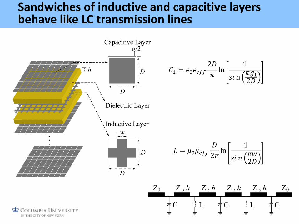
Database was also built for f=80-130 GHz (ECE at DIII-D)

17
Relaxing constraints on absolute phase improves agreement with desired Df(f)
Only relative phase (zone-to-zone) matters
G=“Goal function” (the smaller the better)
K.C. Hammond et al., J Infrared Milli Terahz Waves 34, 437 (2013)

18
Individual fine-tuning of geometrical parameters in each layer further improves the agreement

19
Optimized cells put together and treated as attenuated and delayed dipole-emitters Interference pattern Global lens response

20
Obtained desired RCA for maximum transverse resolution in ECE at at DIII-D.A single lens focuses different f at different locations where that f is EC-emitted.

21
Sidelobes were explained with non-uniform transmissivity across zones grating diffraction maxima

22
Simulations show that varying the lens aperture changes its focal length a diaphragm acting as a zoom!

90 100 110 120 1300.8
1
1.2
1.4
1.6
1.8
2
2.2
Frequency (GHz)
Maj
or
radiu
s, R
maj
(m
)
(a)
Mirror region
Lens region
90 100 110 120 1300.8
1
1.2
1.4
1.6
1.8
2
2.2
Frequency (GHz)
Maj
or
radiu
s, R
maj
(m
)
Mirror region
Lens region
(b)
23
EC-emitting locations are always in focus, with metamaterial lens. They are not in focus with present mirror.
B=-2.0T B=-1.56T
EC-emitting locations
Regions of good focusing
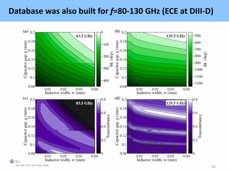
Ink-jet printing is capable of 1-5mm details
24
K. Takano et al., Applied Phys. Expr. 2010Sjctechnology.com
Silver, lines: 3mm, spacing: 15mm Gold, lines: 5mm, spacing: 50mm
Conventional printer CAD Super-fine Printer
Low-power 8-12 GHz lens manufactured using an ink-jet printer and silver-nanoparticle ink
• (show samples)
• Ink = liquid suspension of ~5nm Ag nanoparticles
• Resistivity 3mWcm after 1h sintering at 150-200oC (bulk Ag 1.6mWcm).
• Printed circuit board (PCB) techniques (e.g., laser) also under consideration
• 80-130 GHz might require lithography, laser raster or integrated circuit (IC) nano/microfabrication techniques
• Tests of 8-12 GHz lens starting soon
25

Extension to high power requires modified design and materials • Some motivations:
– Tunable gyrotrons
– Rapid steering of ECCD for NTM stabilization w/o moving mirrors in vessel
– Collective Thomson Scattering
• Simple! Replace:– plastic dielectric
recirculating cooling fluid (freon FC-75)
– Square patches stripes (2 sets, orthogonal)
26

Frequency-controlled Steering
27
• Same num. technique can be used: • Prescribe Df(f) for each cell• Different spatial profiles of Df(f)
• “Super-diffractor”: diffraction grating of metamaterial-enhanced resolving power
• High sensitivity to f important

Conclusions
• Proper array of microfabricated phase-shifters acts as a lens.
• Optimizing its dimensions allows to match a desired dependence of focal length on frequency, including extreme and reverse chromatic aberration.
• Numerical example for 8-12 and 80-130 GHz.
• Lens for 8-12 GHz was manufactured by ink-jet printing (with silver nanoparticle ink) on dielectric substrate.– Inexpensive, fast, suited for low-power, low-frequency.
– Alternatives at high-power and/or high-frequency were discussed.
• Numerical technique can be extended to: – aberration-free lens
– rapid frequency-controlled steering
• With different designs and materials, manufacturing can be extended to high-power heating, current drive & active diagnostics. 28