From ITRS 2.0 to IRDS” · OCTOBER 2017 E3S P.Gargini Paolo Gargini Chairman IRDS, IEUVI Fellow...
62
E3S P.Gargini OCTOBER 2017 Paolo Gargini Chairman IRDS, IEUVI Fellow IEEE, Fellow I - JSAP “Roadmap Evolution: From NTRS to ITRS, From ITRS 2.0 to IRDS” 1
Transcript of From ITRS 2.0 to IRDS” · OCTOBER 2017 E3S P.Gargini Paolo Gargini Chairman IRDS, IEUVI Fellow...
E3S P.GarginiOCTOBER 2017
Paolo Gargini
Chairman IRDS, IEUVI
Fellow IEEE, Fellow I-JSAP
“Roadmap Evolution:
From NTRS to ITRS,
From ITRS 2.0 to IRDS”
1
E3S P.GarginiOCTOBER 2017
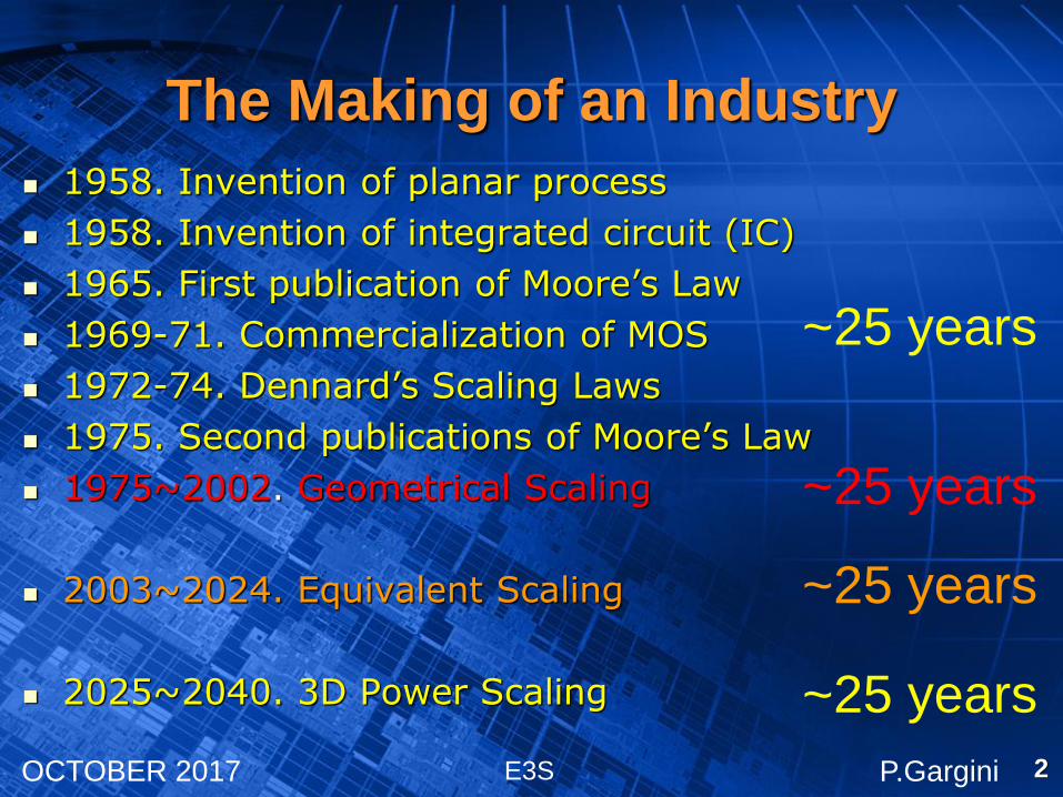
The Making of an Industry
1958. Invention of planar process
1958. Invention of integrated circuit (IC)
1965. First publication of Moore’s Law
1969-71. Commercialization of MOS
1972-74. Dennard’s Scaling Laws
1975. Second publications of Moore’s Law
1975~2002. Geometrical Scaling
2003~2024. Equivalent Scaling
2025~2040. 3D Power Scaling
~25 years
~25 years
~25 years
2
~25 years
E3S P.GarginiOCTOBER 2017
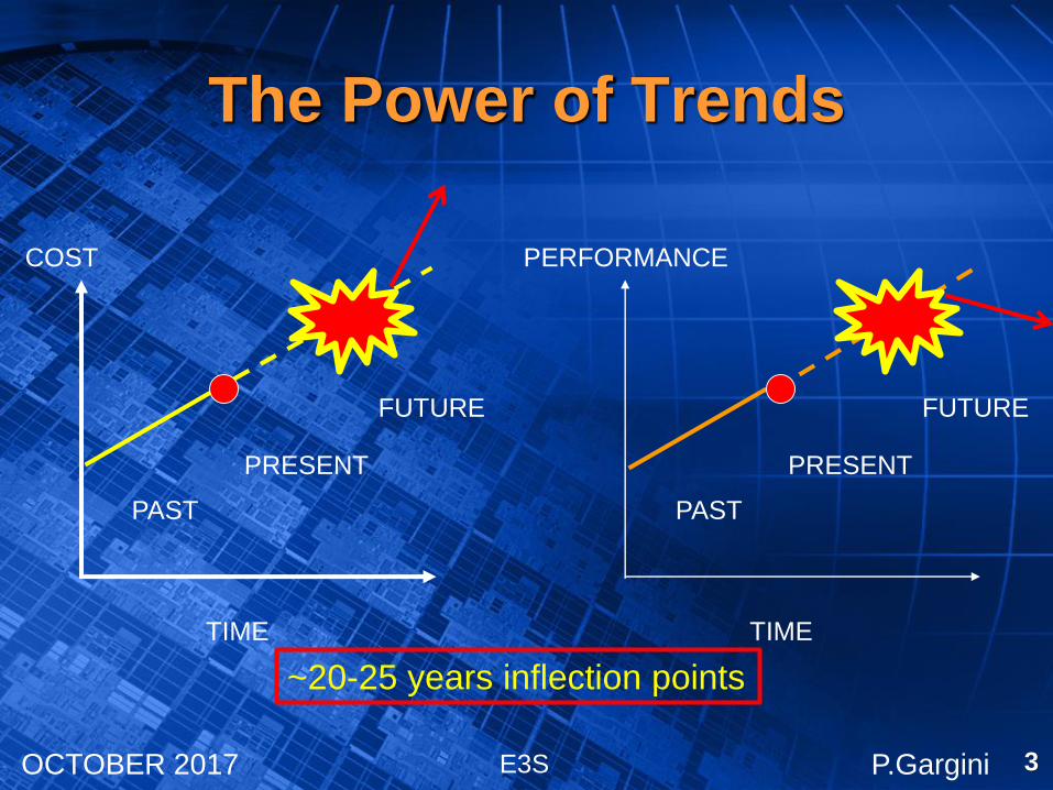
The Power of Trends
TIME
COST
PAST
PRESENT
FUTURE
TIME
PERFORMANCE
PAST
PRESENT
FUTURE
3
~20-25 years inflection points
E3S P.GarginiOCTOBER 2017
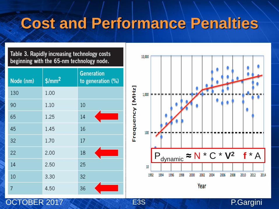
Cost and Performance Penalties
Pdynamic ≈ N * C * V2 * f * A
E3S P.GarginiOCTOBER 2017
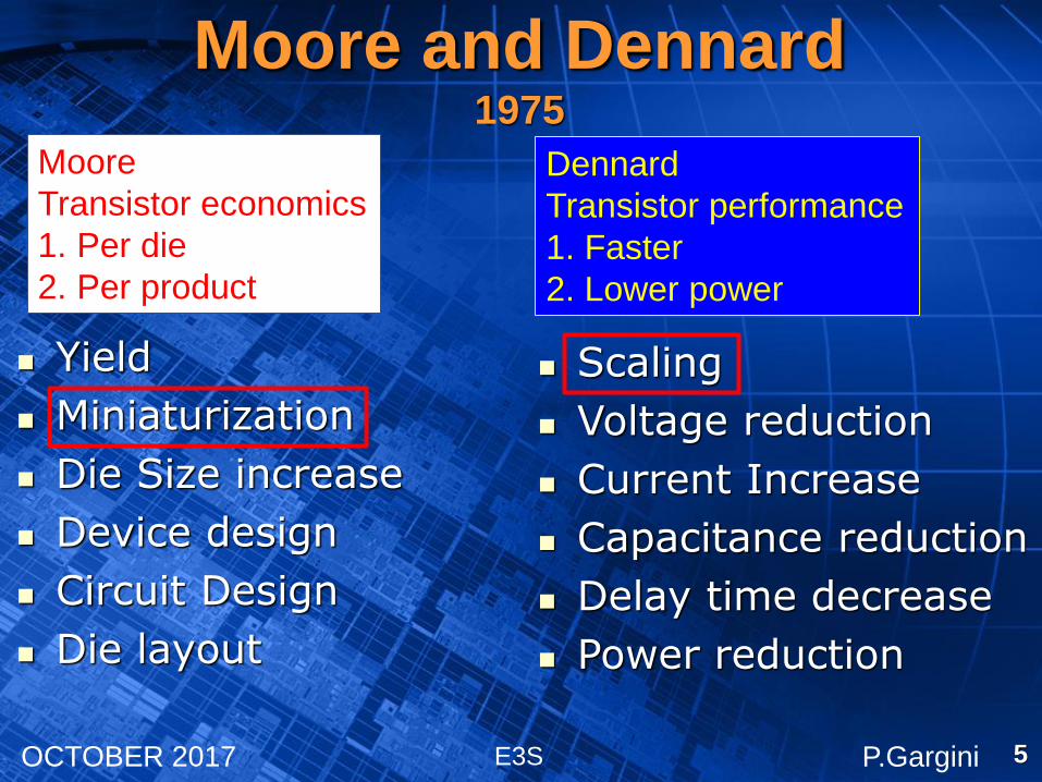
Moore and Dennard1975
Yield
Miniaturization
Die Size increase
Device design
Circuit Design
Die layout
Moore
Transistor economics
1. Per die
2. Per product
Scaling
Voltage reduction
Current Increase
Capacitance reduction
Delay time decrease
Power reduction
Dennard
Transistor performance
1. Faster
2. Lower power
5
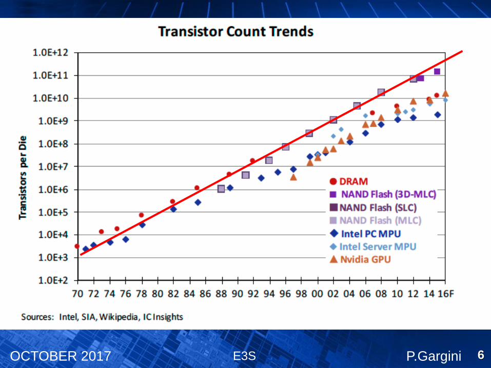
E3S P.GarginiOCTOBER 2017 6
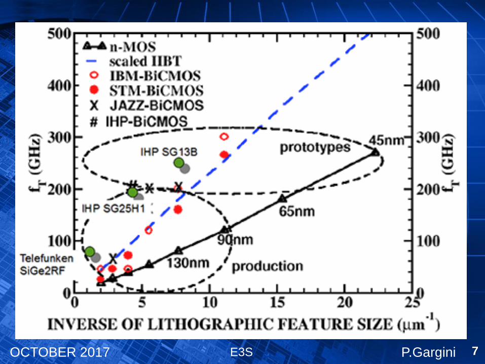
E3S P.GarginiOCTOBER 2017 7
E3S P.GarginiOCTOBER 2017
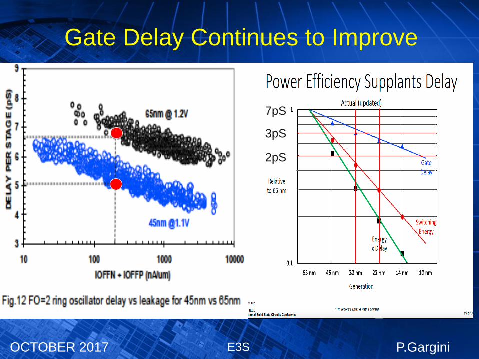
Gate Delay Continues to Improve
7pS
3pS
2pS
E3S P.GarginiOCTOBER 2017
First Age of Scaling(Self-aligned Silicon Gate)
Phase 1
9
~1975-2002
E3S P.GarginiOCTOBER 2017 10
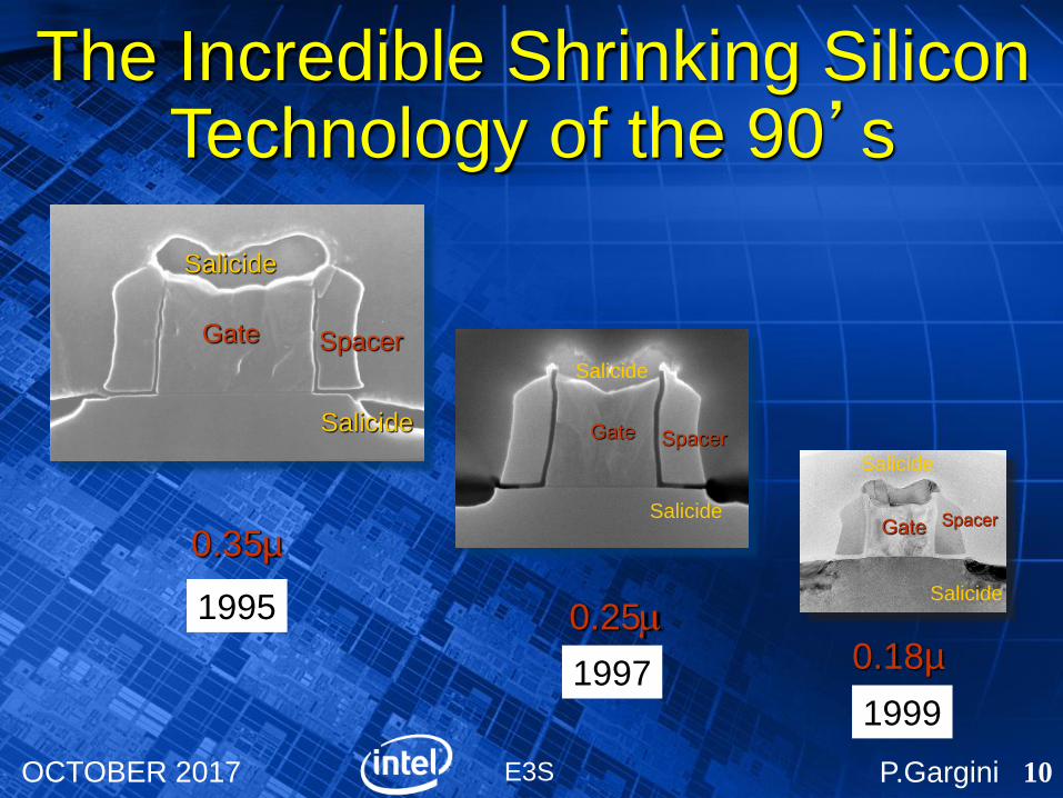
The Incredible Shrinking Silicon Technology of the 90’s
0.35 µ
Gate
Salicide
Spacer
Salicide
1995 m0.25
Salicide
Gate Spacer
Salicide
1997 0.18µ
Gate Spacer
Salicide
Salicide
1999
E3S P.GarginiOCTOBER 2017
NTRS1991,1992,1994 and1997
11
E3S P.GarginiOCTOBER 2017
~20-25 Years Later
1975-1997
12
E3S P.GarginiOCTOBER 2017
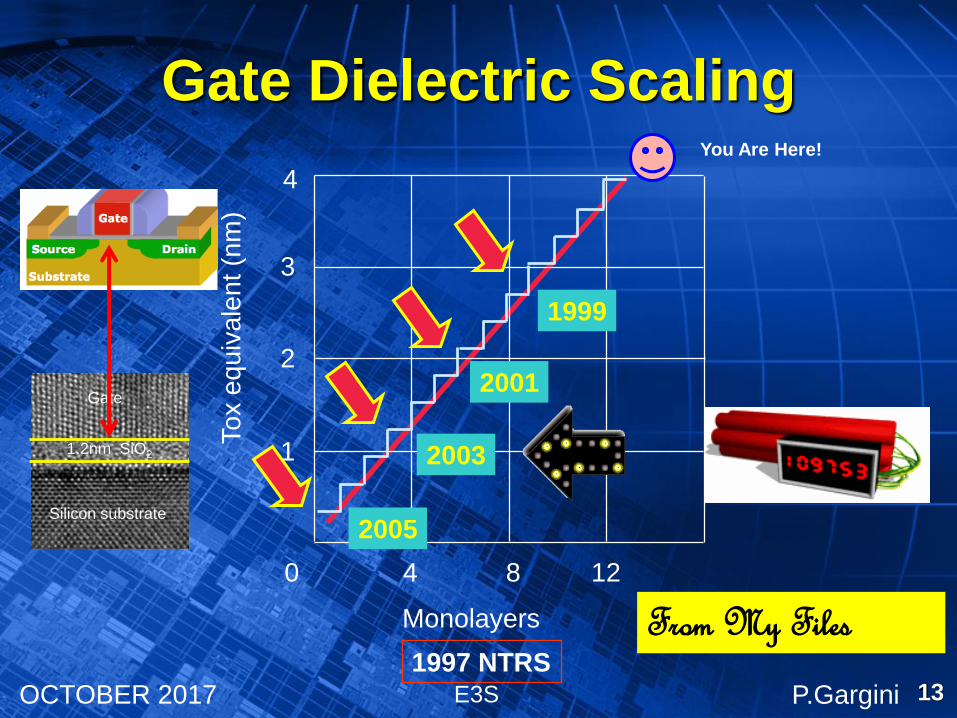
Gate Dielectric Scaling
1
2
3
To
x e
qu
iva
len
t (n
m)
4 8 12
Monolayers
4
0
1999
2001
2003
2005
1997 NTRS
You Are Here!
Silicon substrate
1.2nm SiO2
Gate
From My Files
13

E3S P.GarginiOCTOBER 2017
The Power of Trends
TIME
COST
PAST
PRESENT
FUTURE
TIME
PERFORMANCE
PAST
PRESENT
FUTURE
14

E3S P.GarginiOCTOBER 2017
Audience Reaction to the News
15
E3S P.GarginiOCTOBER 2017
ITRS 1.0
1998
16
E3S P.GarginiOCTOBER 2017
Second Age of Scaling:(Equivalent Scaling)
Phase 2
17
E3S P.GarginiOCTOBER 2017
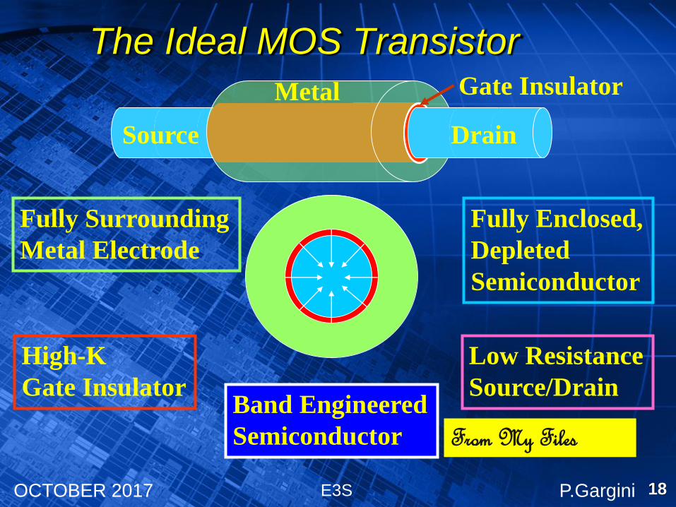
The Ideal MOS Transistor
From My Files
Fully Surrounding
Metal Electrode
High-K
Gate Insulator
Fully Enclosed,
Depleted
Semiconductor
Low Resistance
Source/Drain
DrainSource
Metal Gate Insulator
Band Engineered
Semiconductor
18

E3S P.GarginiOCTOBER 2017 19
E3S P.GarginiOCTOBER 2017
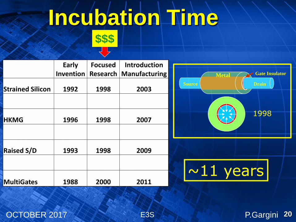
Incubation Time
EarlyInvention
FocusedResearch
IntroductionManufacturing
Strained Silicon 1992 1998 2003
HKMG 1996 1998 2007
Raised S/D 1993 1998 2009
MultiGates 1988 2000 2011~11 years
DrainSource
Metal Gate Insulator
1998
20
$$$
E3S P.GarginiOCTOBER 2017 21
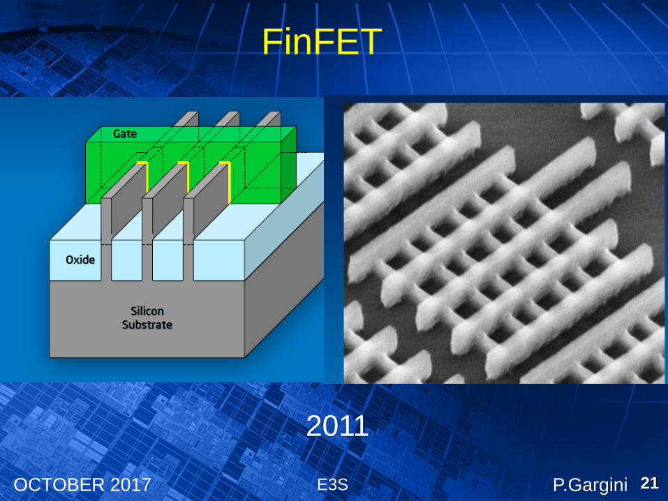
2011
FinFET
E3S P.GarginiOCTOBER 2017
~20-25 Years Later
1997-2025
22
E3S P.GarginiOCTOBER 2017
5
7
10
Te
ch
no
log
y N
od
e (
nm
)
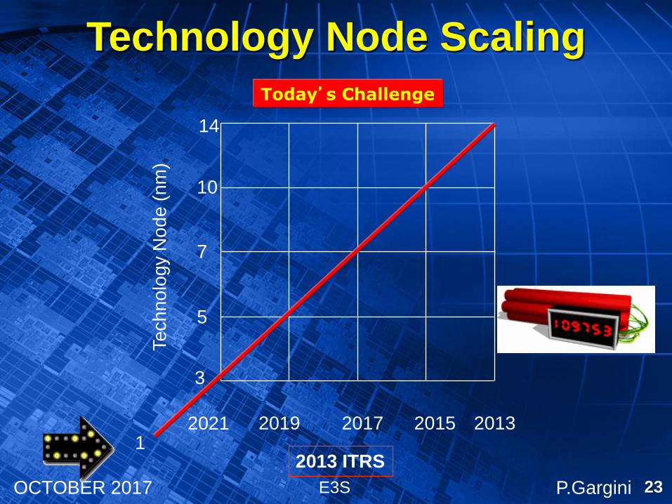
2017 2015 2013
14
2019
2013 ITRS
2021
3
1
Technology Node Scaling
Today’s Challenge
23

E3S P.GarginiOCTOBER 2017
The Power of Trends
TIME
COST
PAST
PRESENT
FUTURE
TIME
PERFORMANCE
PAST
PRESENT
FUTURE
24
~20-25 years inflection points

E3S P.GarginiOCTOBER 2017 25
E3S P.GarginiOCTOBER 2017
3D Manhattan Solution
26
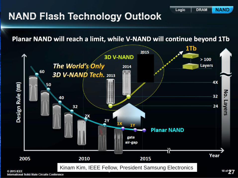
E3S P.GarginiOCTOBER 2017 27Kinam Kim, IEEE Fellow, President Samsung Electronics
27
E3S P.GarginiOCTOBER 2017
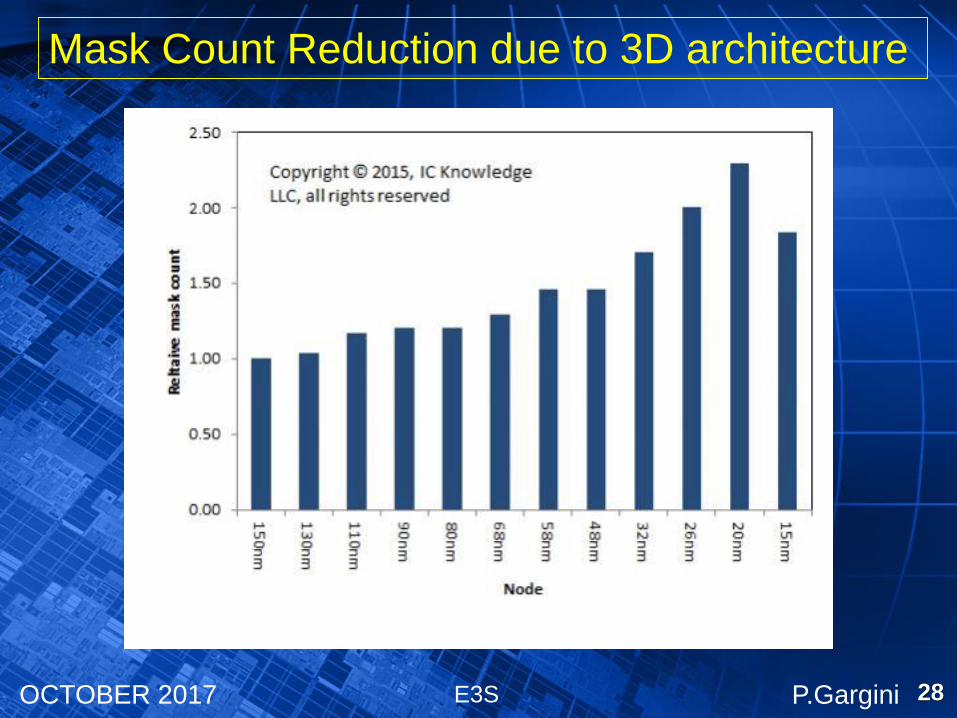
Mask Count Reduction due to 3D architecture
28
E3S P.GarginiOCTOBER 2017
ITRS 2.0
http://www.itrs2.net
29
E3S P.GarginiOCTOBER 2017
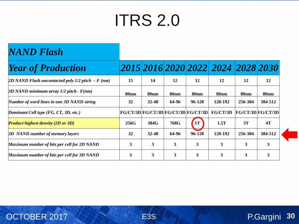
NAND Flash
Year of Production 2015 2016 2020 2022 2024 2028 20302D NAND Flash uncontacted poly 1/2 pitch – F (nm) 15 14 12 12 12 12 12
3D NAND minimum array 1/2 pitch - F(nm) 80nm 80nm 80nm 80nm 80nm 80nm 80nm
Number of word lines in one 3D NAND string 32 32-48 64-96 96-128 128-192 256-384 384-512
Dominant Cell type (FG, CT, 3D, etc.) FG/CT/3D FG/CT/3D FG/CT/3D FG/CT/3D FG/CT/3D FG/CT/3D FG/CT/3D
Product highest density (2D or 3D) 256G 384G 768G 1T 1.5T 3T 4T
3D NAND number of memory layers 32 32-48 64-96 96-128 128-192 256-384 384-512
Maximum number of bits per cell for 2D NAND 3 3 3 3 3 3 3
Maximum number of bits per cell for 3D NAND 3 3 3 3 3 3 3
30
ITRS 2.0
E3S P.GarginiOCTOBER 2017 31
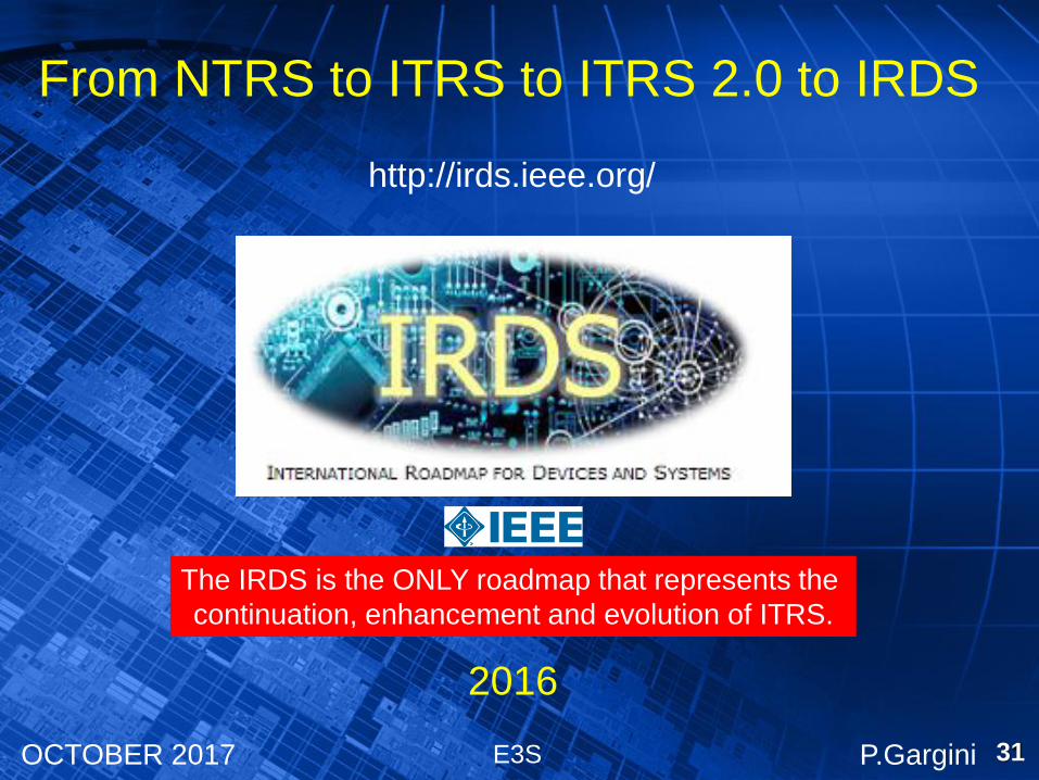
From NTRS to ITRS to ITRS 2.0 to IRDS
The IRDS is the ONLY roadmap that represents the
continuation, enhancement and evolution of ITRS.
http://irds.ieee.org/
2016
E3S P.GarginiOCTOBER 2017
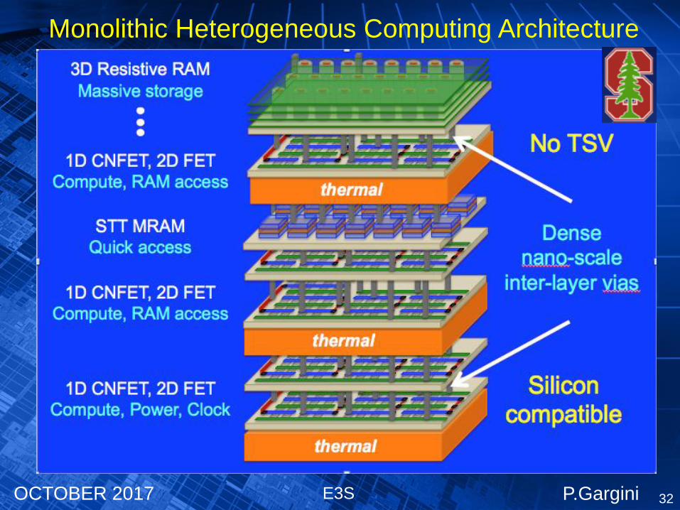
Monolithic Heterogeneous Computing Architecture
32
E3S P.GarginiOCTOBER 2017
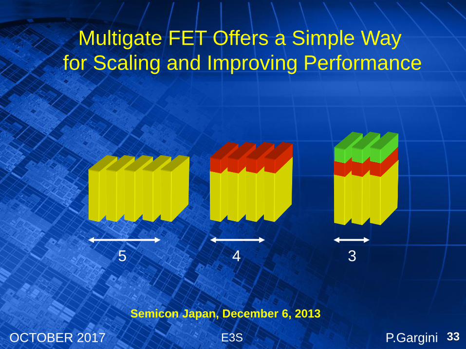
Multigate FET Offers a Simple Way
for Scaling and Improving Performance
5 4 3
Semicon Japan, December 6, 2013
33
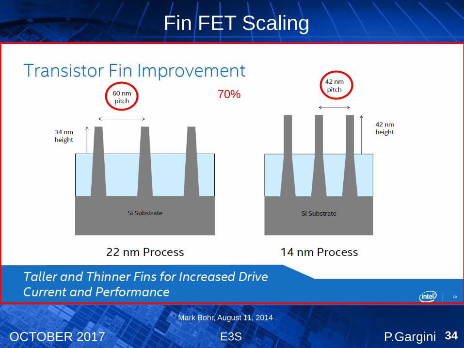
E3S P.GarginiOCTOBER 2017 34
Mark Bohr, August 11, 2014
Fin FET Scaling
70%
E3S P.GarginiOCTOBER 2017
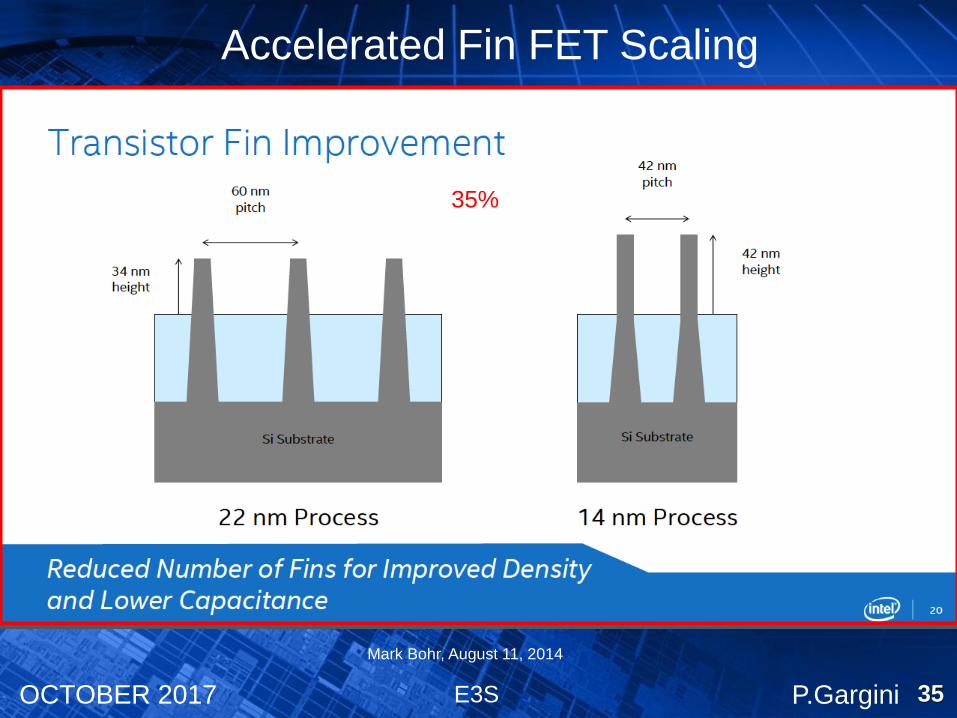
Mark Bohr, August 11, 2014
35
Accelerated Fin FET Scaling
35%
E3S P.GarginiOCTOBER 2017
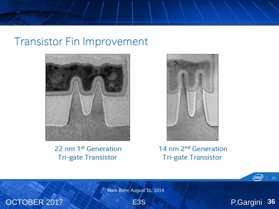
Mark Bohr, August 11, 2014
36
E3S P.GarginiOCTOBER 2017
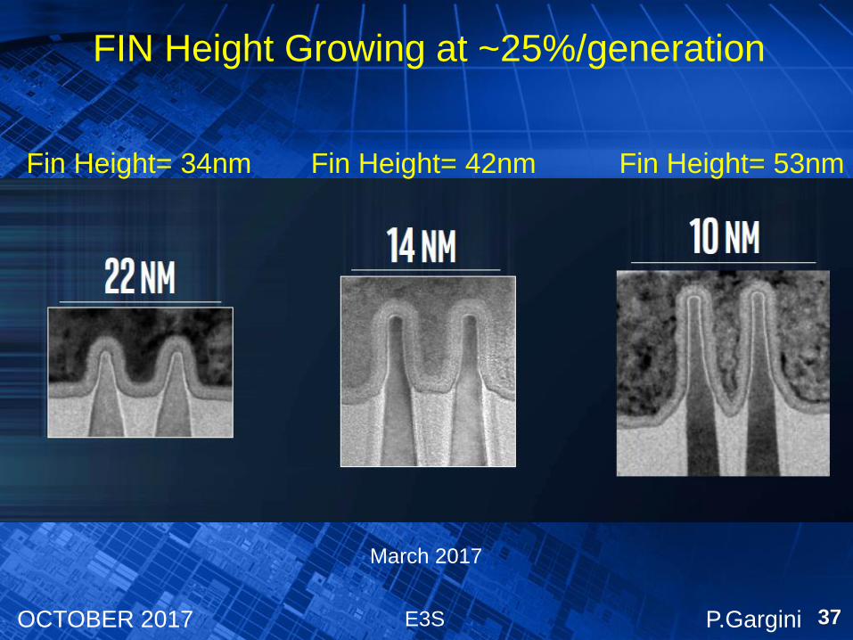
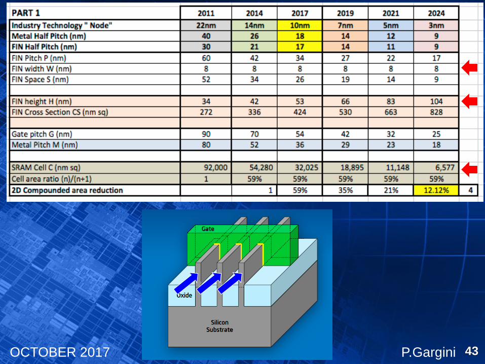
March 2017
Fin Height= 34nm Fin Height= 42nm Fin Height= 53nm
37
FIN Height Growing at ~25%/generation
E3S P.GarginiOCTOBER 2017 38
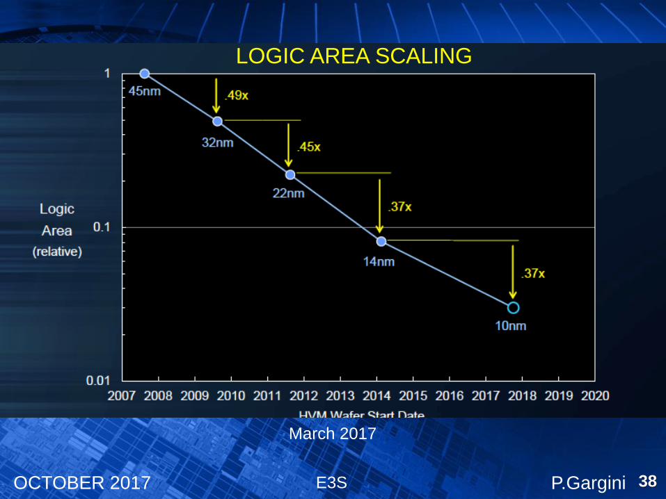
LOGIC AREA SCALING
March 2017
E3S P.GarginiOCTOBER 2017 39
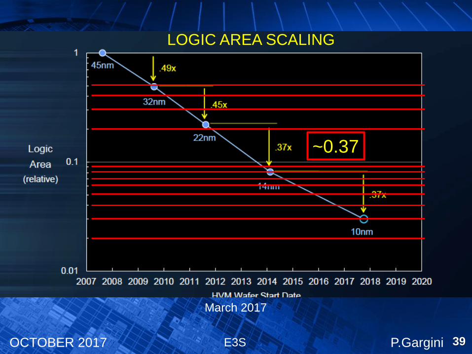
LOGIC AREA SCALING
March 2017
~0.37
E3S P.GarginiOCTOBER 2017 40
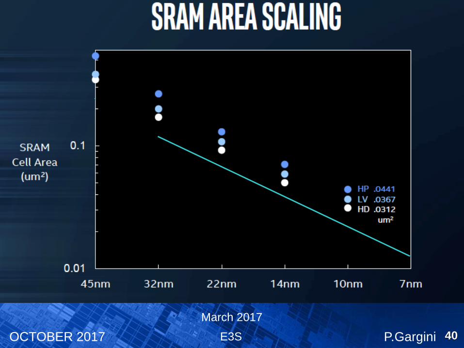
March 2017
E3S P.GarginiOCTOBER 2017
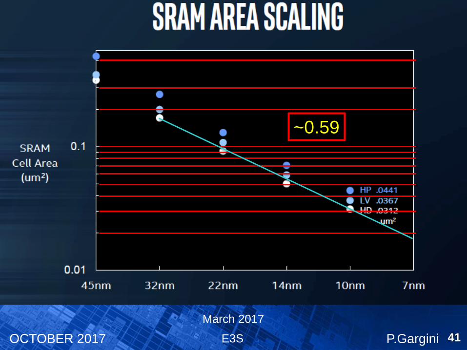
~0.59
41
March 2017
E3S P.GarginiOCTOBER 2017
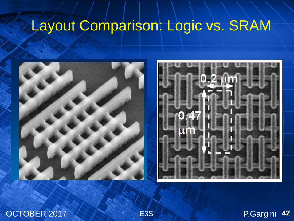
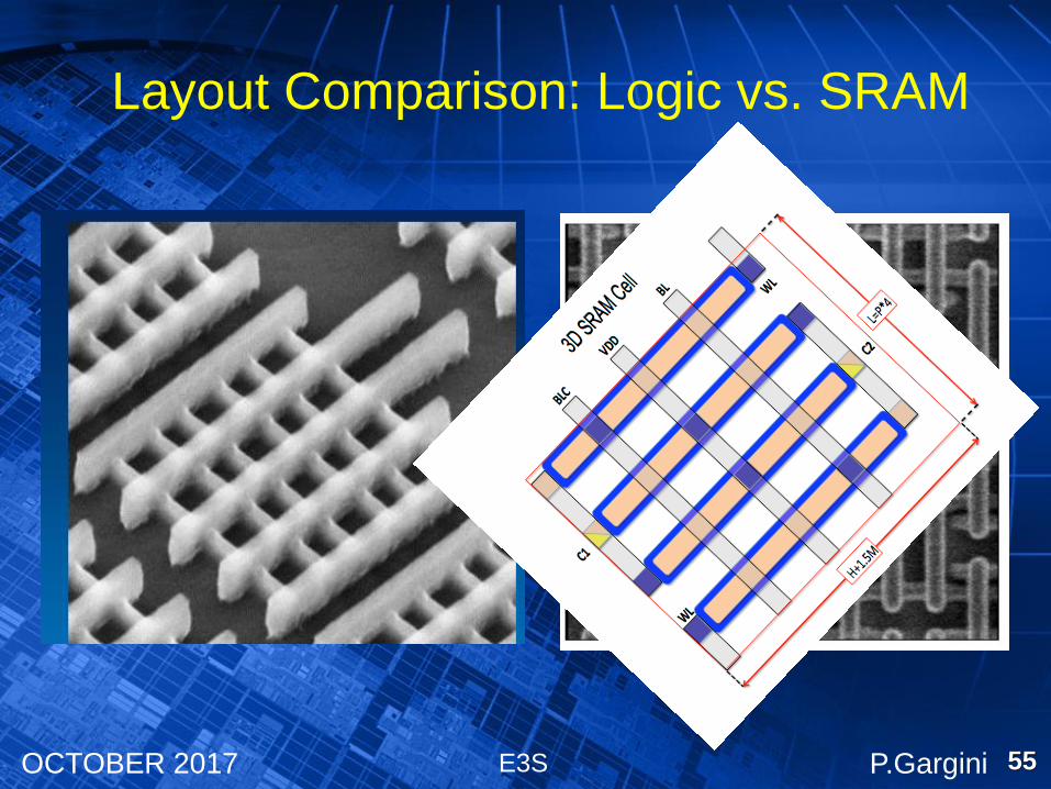
Layout Comparison: Logic vs. SRAM
42
E3S P.GarginiOCTOBER 2017 43
E3S P.GarginiOCTOBER 2017 44
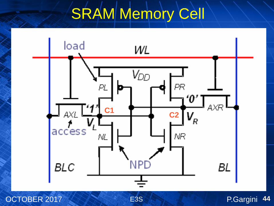
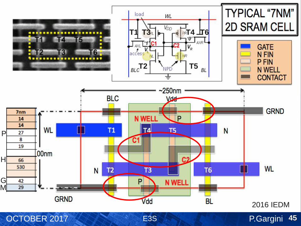
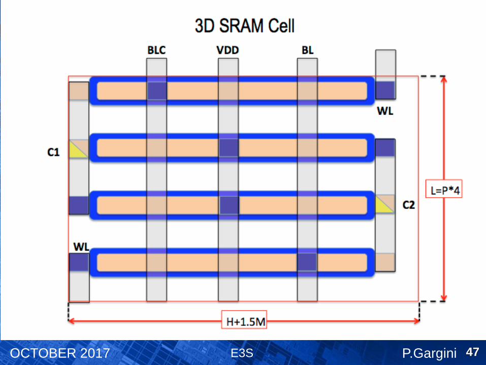
SRAM Memory Cell
C1C2
E3S P.GarginiOCTOBER 2017
P
H
MG
2016 IEDM
45
T1
T2
T6
T5
T3 T4
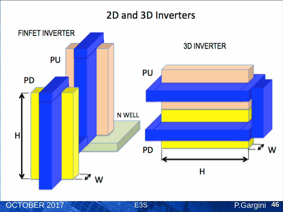
E3S P.GarginiOCTOBER 2017 46
E3S P.GarginiOCTOBER 2017 47
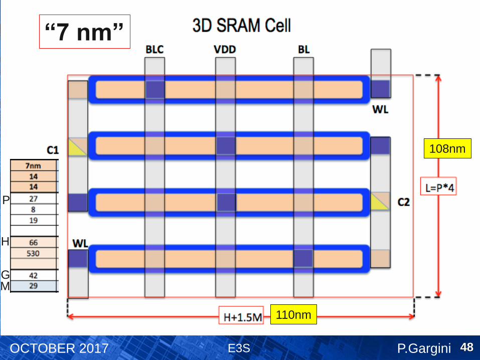
E3S P.GarginiOCTOBER 2017
“7 nm”
108nm
110nm
P
H
MG
48
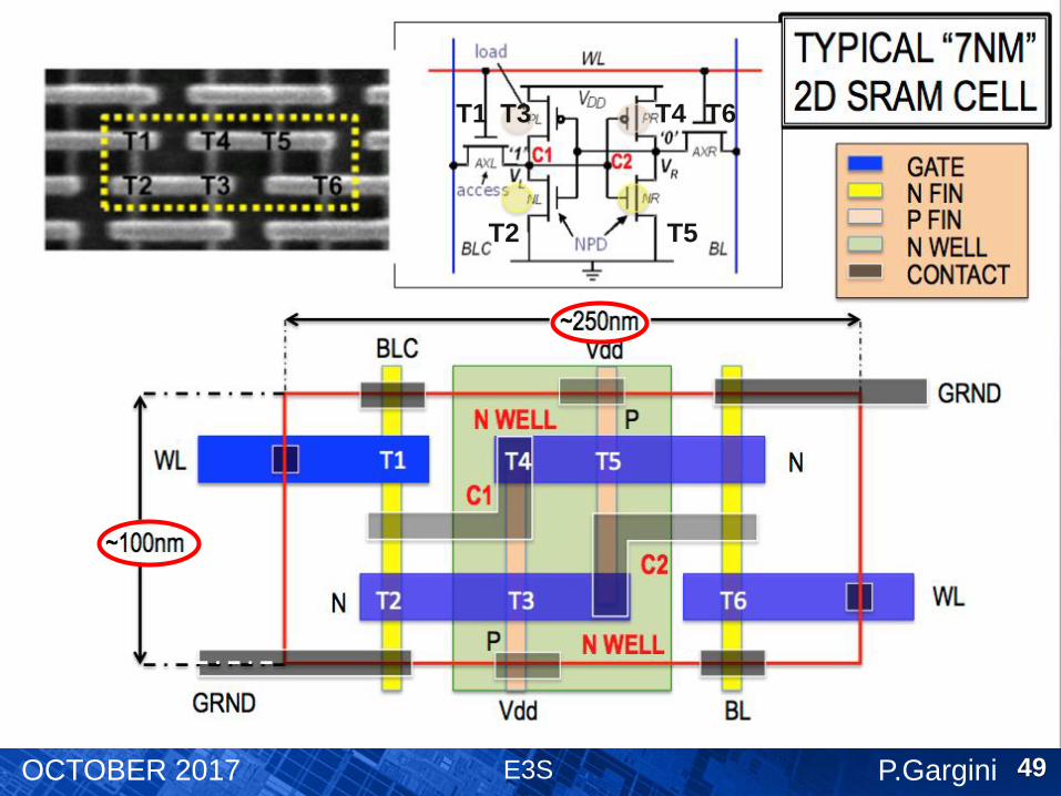
E3S P.GarginiOCTOBER 2017 49
T1
T2
T6
T5
T3 T4
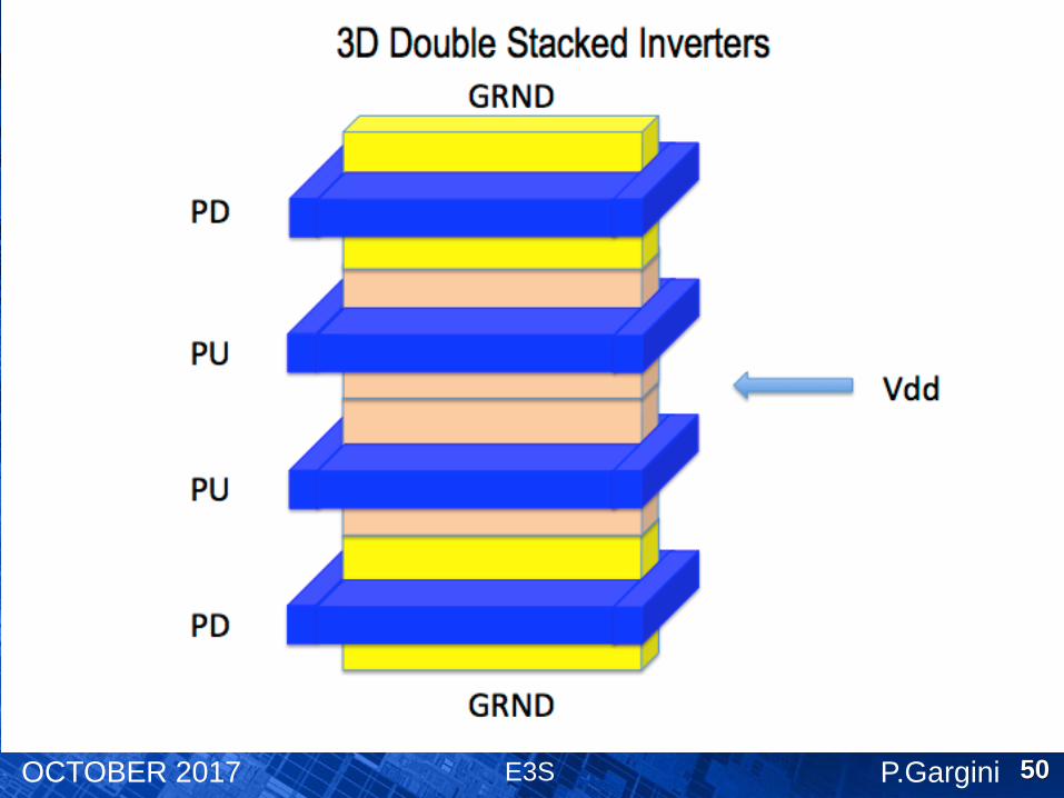
E3S P.GarginiOCTOBER 2017 50
E3S P.GarginiOCTOBER 2017 51

E3S P.GarginiOCTOBER 2017
The Power of Trends
TIME
COST
PAST
PRESENT
FUTURE
TIME
PERFORMANCE
PAST
PRESENT
FUTURE
52
~20-25 years inflection points
E3S P.GarginiOCTOBER 2017
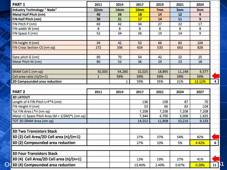
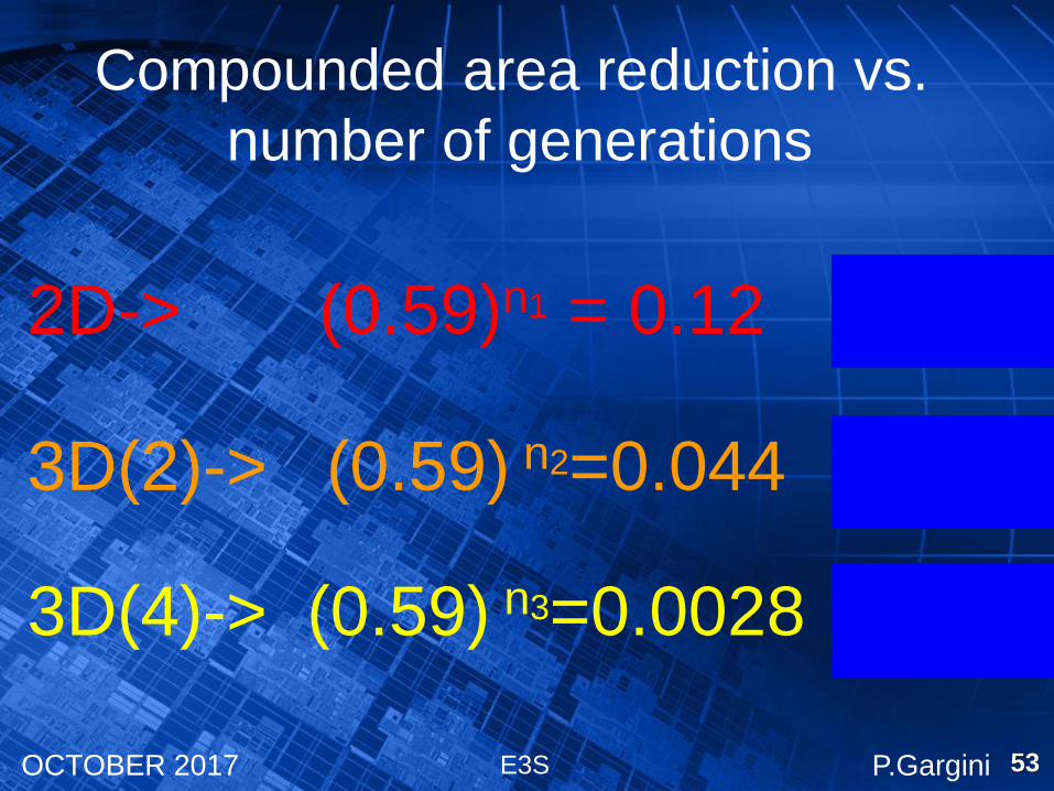
2D-> (0.59)n1 = 0.12 n1=4
3D(2)-> (0.59) n2=0.044
3D(4)-> (0.59) n3=0.0028
Compounded area reduction vs.
number of generations
n2=6
n3=11
53

E3S P.GarginiOCTOBER 2017
2D-> (0.50)n1 = 0.12 N1=3
3D(2)-> (0.50) n2=0.044
3D(4)-> (0.50) n3=0.0028
Compounded area reduction vs.
number of generations
N2=5
N3=9
54
E3S P.GarginiOCTOBER 2017
Layout Comparison: Logic vs. SRAM
55
E3S P.GarginiOCTOBER 2017
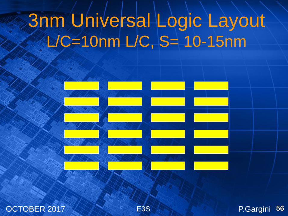
3nm Universal Logic LayoutL/C=10nm L/C, S= 10-15nm
56
E3S P.GarginiOCTOBER 2017
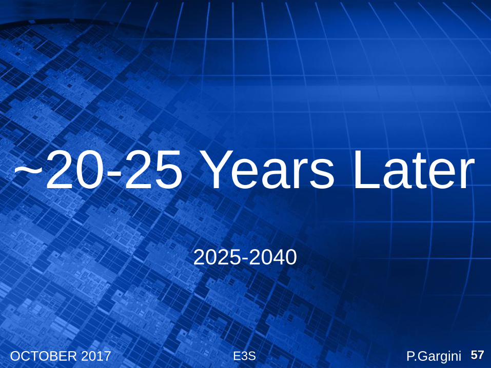
~20-25 Years Later
2025-2040
57
E3S P.GarginiOCTOBER 2017
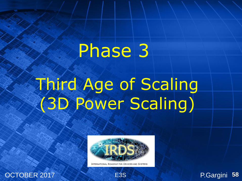
Third Age of Scaling(3D Power Scaling)
Phase 3
58
E3S P.GarginiOCTOBER 2017
3D
59
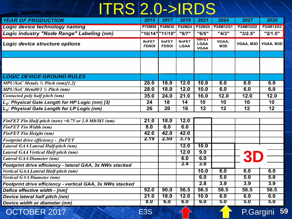
ITRS 2.0->IRDS
E3S P.GarginiOCTOBER 2017
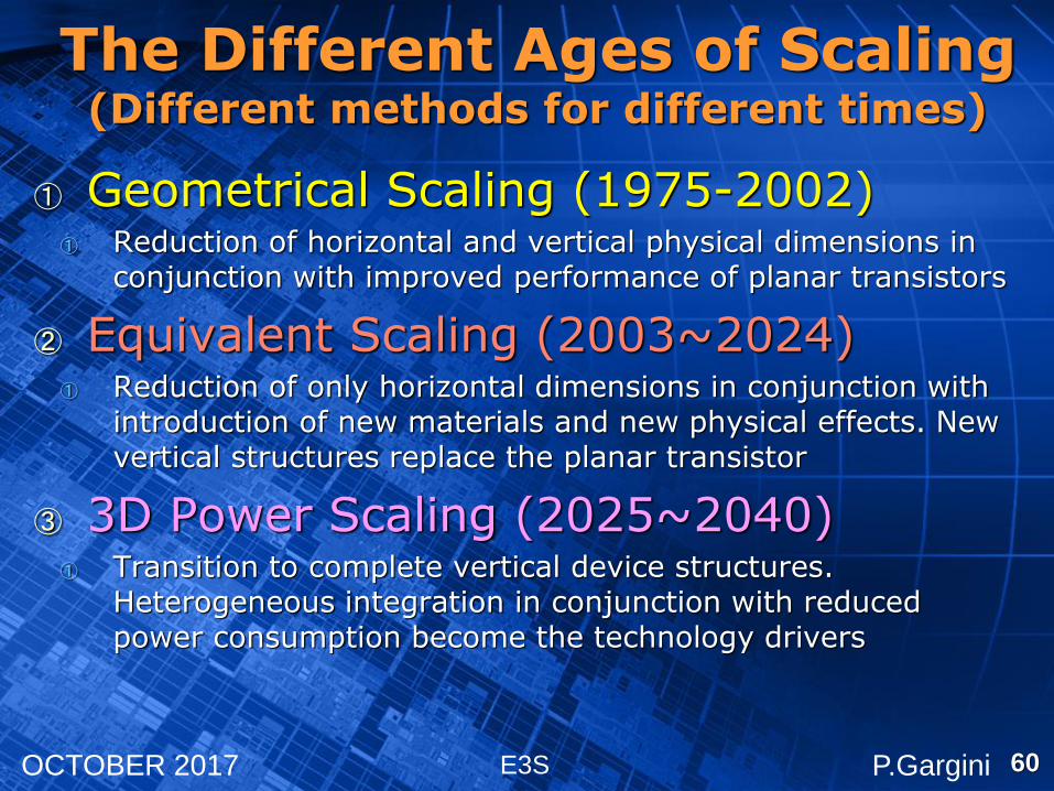
The Different Ages of Scaling(Different methods for different times)
① Geometrical Scaling (1975-2002)① Reduction of horizontal and vertical physical dimensions in
conjunction with improved performance of planar transistors
② Equivalent Scaling (2003~2024)① Reduction of only horizontal dimensions in conjunction with
introduction of new materials and new physical effects. New vertical structures replace the planar transistor
③ 3D Power Scaling (2025~2040)① Transition to complete vertical device structures.
Heterogeneous integration in conjunction with reduced power consumption become the technology drivers
60
E3S P.GarginiOCTOBER 2017
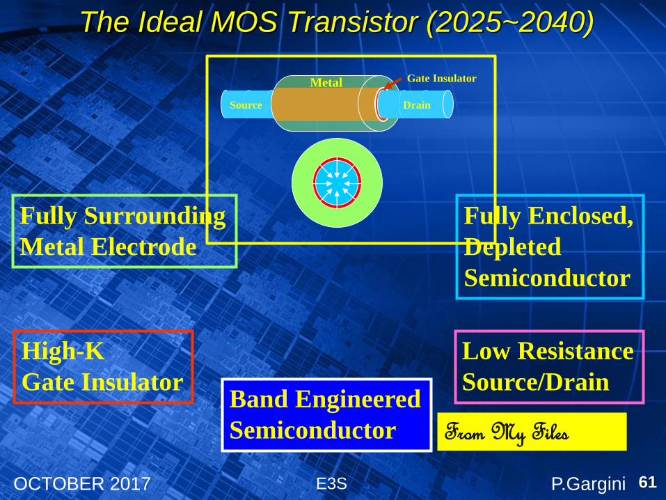
The Ideal MOS Transistor (2025~2040)
From My Files
Fully Surrounding
Metal Electrode
High-K
Gate Insulator
Fully Enclosed,
Depleted
Semiconductor
Low Resistance
Source/DrainBand Engineered
Semiconductor
DrainSource
Metal Gate Insulator
61

E3S P.GarginiOCTOBER 2017
“How Long will the Industry
Delay the Conversion to
3D Monolithic Integration ?”
62
Thank you!