
Frequency-selective surfaces to enhance performance of ...
9
1716 IEEE TRANSACTIONS ON ANTENNAS AND PROPAGATION, VOL. 50, NO. 12, DECEMBER 2002 Frequency-Selective Surfaces to Enhance Performance of Broad-Band Reconfigurable Arrays Yunus E. Erdemli, Member, IEEE, Kubilay Sertel, Roland A. Gilbert, Member, IEEE, Daniel E. Wright, and John L. Volakis, Fellow, IEEE Abstract—In this paper, we present a novel frequency-selective surface (FSS) design aimed at enhancing the performance of broad-band reconfigurable antenna apertures. In particular, reconfigurable printed dipole arrays are examined in the presence of a multilayer FSS. Of particular interest is the design of FSS structures whose reflection coefficient has prespecified phase response over a broad set of frequencies. Previous FSSs primarily considered designs on the basis of the reflection-coefficient am- plitude and were intended for radome applications rather than substrates. Designing FSSs subject to phase requirements will be seen to require some compromise in the magnitude. Broad-band requirements also present us with a need for noncommensurate FSS designs. Index Terms—Broad-band substrate design, hybrid finite-ele- ment boundary-integral method, multilayer frequency-selective surfaces, noncommensurate structures, reconfigurable antenna apertures. I. INTRODUCTION C ONFORMAL antennas are often printed on a planar or curved substrate surface. However, typical substrate configurations are narrowband, and thicker substrates result in low efficiencies due to surface wave coupling. Perforated or bandgap substrates have recently been used to increase the efficiency of printed antennas on thicker substrates [1], [2]. However, these approaches are still applicable only to narrowband or multiband antenna structures. When traditional broad-band antennas such as log-periodics are printed on substrates, their bandwidth characteristics are altered, and one approach to regain the broad-band behavior of the antenna element is to employ frequency-dependent substrates or ground planes (GPs). This can be achieved by using multiple layers of frequency selective surfaces (FSSs) [3] as part of the substrate in a manner similar to that used for designing broad-band microwave filters. Each screen is resonant at a given frequency and is placed a distance away from the antenna’s surface, Manuscript received November 10, 2000; revised May 31, 2001. This work was supported by DARPA/RECAP Program. Y. E. Erdemli, was with the Radiation Laboratory, Electrical Engineering and Computer Science Department, University of Michigan, Ann Arbor, MI 48109-2122 USA. He is now with the Department of Electronics and Computer Education, Kocaeli University, 41050 Ismit, Turkey. K. Sertel is with the Radiation Laboratory, Electrical Engineering and Com- puter Science Department, University of Michigan, Ann Arbor, MI 48109-2122 USA. R. A. Gilbert and D. E. Wright are with BAE Systems, Nashua, NH 03060-0868 USA. J. L. Volakis is with The Ohio State University, Columbus, OH 43210 USA. Digital Object Identifier 10.1109/TAP.2002.807377 Fig. 1. Reconfigurable antenna aperture (RECAP) over a multilayer FSS/FSV structure. Fig. 2. Coherence between antenna radiation and reflections from the substrate provides broad-band operation. where refers to the wavelength at the screen’s resonance frequency. A multilayer FSS or frequency-selective volume (FSV) con- figuration [4]–[6] is needed for optimizing the performance of a broad-band antenna. Such a structure is illustrated in Fig. 1. In this paper, we examine various designs of such volumetric pe- riodic surfaces that can be used to enhance the performance of reconfigurable broad-band antenna arrays (see Fig. 1). Of partic- ular interest is the development of such multilayer FSSs, which reflect with prespecified phase and amplitude of the reflection coefficient over a broad set of frequencies. When the phase is ac- tually maintained near zero degrees, such FSSs serve to emulate magnetic GPs. As such, they can substantially enhance the ra- diation properties of printed antennas placed over the FSS since the reflected field will be in phase with that directly radiated by the antenna itself (see Fig. 2). When the FSS is designed to de- liver nearly constant phase over a broad bandwidth, substantial 0018-926X/02$17.00 © 2002 IEEE
Transcript of Frequency-selective surfaces to enhance performance of ...
1716 IEEE TRANSACTIONS ON ANTENNAS AND PROPAGATION, VOL. 50, NO. 12, DECEMBER 2002
Frequency-Selective Surfaces to EnhancePerformance of Broad-Band Reconfigurable Arrays
Yunus E. Erdemli, Member, IEEE, Kubilay Sertel, Roland A. Gilbert, Member, IEEE, Daniel E. Wright, andJohn L. Volakis, Fellow, IEEE
Abstract—In this paper, we present a novel frequency-selectivesurface (FSS) design aimed at enhancing the performance ofbroad-band reconfigurable antenna apertures. In particular,reconfigurable printed dipole arrays are examined in the presenceof a multilayer FSS. Of particular interest is the design of FSSstructures whose reflection coefficient has prespecified phaseresponse over a broad set of frequencies. Previous FSSs primarilyconsidered designs on the basis of the reflection-coefficient am-plitude and were intended for radome applications rather thansubstrates. Designing FSSs subject to phase requirements will beseen to require some compromise in the magnitude. Broad-bandrequirements also present us with a need for noncommensurateFSS designs.
Index Terms—Broad-band substrate design, hybrid finite-ele-ment boundary-integral method, multilayer frequency-selectivesurfaces, noncommensurate structures, reconfigurable antennaapertures.
I. INTRODUCTION
CONFORMAL antennas are often printed on a planaror curved substrate surface. However, typical substrate
configurations are narrowband, and thicker substrates resultin low efficiencies due to surface wave coupling. Perforatedor bandgap substrates have recently been used to increasethe efficiency of printed antennas on thicker substrates [1],[2]. However, these approaches are still applicable only tonarrowband or multiband antenna structures. When traditionalbroad-band antennas such as log-periodics are printed onsubstrates, their bandwidth characteristics are altered, and oneapproach to regain the broad-band behavior of the antennaelement is to employ frequency-dependent substrates or groundplanes (GPs). This can be achieved by using multiple layers offrequency selective surfaces (FSSs) [3] as part of the substratein a manner similar to that used for designing broad-bandmicrowave filters. Each screen is resonant at a given frequencyand is placed a distance away from the antenna’s surface,
Manuscript received November 10, 2000; revised May 31, 2001. This workwas supported by DARPA/RECAP Program.
Y. E. Erdemli, was with the Radiation Laboratory, Electrical Engineeringand Computer Science Department, University of Michigan, Ann Arbor, MI48109-2122 USA. He is now with the Department of Electronics and ComputerEducation, Kocaeli University, 41050 Ismit, Turkey.
K. Sertel is with the Radiation Laboratory, Electrical Engineering and Com-puter Science Department, University of Michigan, Ann Arbor, MI 48109-2122USA.
R. A. Gilbert and D. E. Wright are with BAE Systems, Nashua, NH03060-0868 USA.
J. L. Volakis is with The Ohio State University, Columbus, OH 43210 USA.Digital Object Identifier 10.1109/TAP.2002.807377
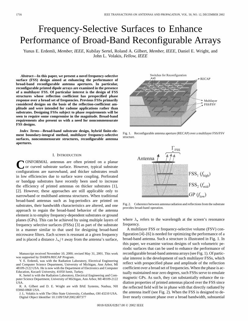
Fig. 1. Reconfigurable antenna aperture (RECAP) over a multilayer FSS/FSVstructure.
Fig. 2. Coherence between antenna radiation and reflections from the substrateprovides broad-band operation.
where refers to the wavelength at the screen’s resonancefrequency.
A multilayer FSS or frequency-selective volume (FSV) con-figuration [4]–[6] is needed for optimizing the performance of abroad-band antenna. Such a structure is illustrated in Fig. 1. Inthis paper, we examine various designs of such volumetric pe-riodic surfaces that can be used to enhance the performance ofreconfigurable broad-band antenna arrays (see Fig. 1). Of partic-ular interest is the development of such multilayer FSSs, whichreflect with prespecified phase and amplitude of the reflectioncoefficient over a broad set of frequencies. When the phase is ac-tually maintained near zero degrees, such FSSs serve to emulatemagnetic GPs. As such, they can substantially enhance the ra-diation properties of printed antennas placed over the FSS sincethe reflected field will be in phase with that directly radiated bythe antenna itself (see Fig. 2). When the FSS is designed to de-liver nearly constant phase over a broad bandwidth, substantial
0018-926X/02$17.00 © 2002 IEEE
ERDEMLI et al.: FREQUENCY-SELECTIVE SURFACES 1717
Fig. 3. Prismatic FE mesh for a commensurate unit cell.
gain enhancement can be achieved over a wide range of frequen-cies. In the past, FSS designs were mostly concerned with am-plitude responses. For FSS GPs, the emphasis is on phase. Oneway to achieve smooth phase responses is to compromise theamplitude response and in this paper, we demonstrate this effect.In addition, using full-wave finite element-boundary integral(FE-BI) simulations, we demonstrate the bandwidth improve-ments achieved for a dipole array on such an FSS. Reconfigu-ration of the dipole is also considered in our study. In this case,the dipole length is altered (using diode or MEMS switches) tooperate at a different band without a need for changing the FSSdesign that serves as a “substrate.” Broad bandwidth require-ments also present us with a need for noncommensurate FSSdesigns. Hence, modeling of multilayer FSSs with different pe-riodicities [7] is another important issue that will be addressedin the paper.
II. FULL-WAVE ANALYSIS
The hybrid FE-BI method [8] is used for the analysis of mul-tilayer FSS structures of interest. An important aspect of thishybrid technique is the ability to simulate and design structuresthat are complex in geometry and incorporate a variety of ma-terials. A multilayer FSS or a FSV in the presence of an an-tenna array is one such structure (Fig. 1). As is often the case,the highly adaptable FE method is used for modeling the mul-tilayer dielectric region of the array, whereas the BI serves as ameans of truncating the finite-element mesh. The BI submatrixtypically consumes most of the CPU requirements. Therefore,a recently introduced scheme referred to as the fast spectral-do-main algorithm (FSDA) is employed to speed up the BI calcu-lations in the context of iterative solvers [9]. As compared tothe adaptive-integral method (AIM), the FSDA often providestwo orders of magnitude faster solutions with memory as well asCPU complexity of . Thus, the adaptability of the FE-BImethod along with the speed-up advantage of the FSDA servesas a very efficient analysis tool while designing antenna arrayswith multilayer FSSs.
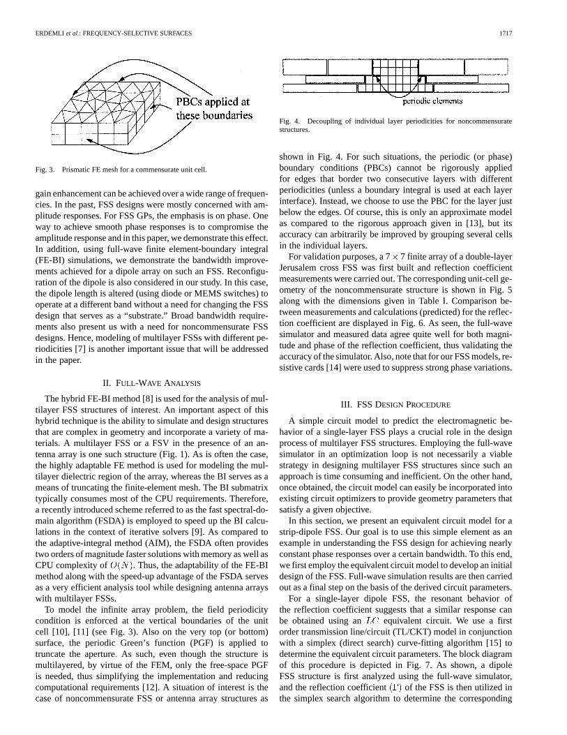
To model the infinite array problem, the field periodicitycondition is enforced at the vertical boundaries of the unitcell [10], [11] (see Fig. 3). Also on the very top (or bottom)surface, the periodic Green’s function (PGF) is applied totruncate the aperture. As such, even though the structure ismultilayered, by virtue of the FEM, only the free-space PGFis needed, thus simplifying the implementation and reducingcomputational requirements [12]. A situation of interest is thecase of noncommensurate FSS or antenna array structures as
Fig. 4. Decoupling of individual layer periodicities for noncommensuratestructures.
shown in Fig. 4. For such situations, the periodic (or phase)boundary conditions (PBCs) cannot be rigorously appliedfor edges that border two consecutive layers with differentperiodicities (unless a boundary integral is used at each layerinterface). Instead, we choose to use the PBC for the layer justbelow the edges. Of course, this is only an approximate modelas compared to the rigorous approach given in [13], but itsaccuracy can arbitrarily be improved by grouping several cellsin the individual layers.
For validation purposes, a 77 finite array of a double-layerJerusalem cross FSS was first built and reflection coefficientmeasurements were carried out. The corresponding unit-cell ge-ometry of the noncommensurate structure is shown in Fig. 5along with the dimensions given in Table I. Comparison be-tween measurements and calculations (predicted) for the reflec-tion coefficient are displayed in Fig. 6. As seen, the full-wavesimulator and measured data agree quite well for both magni-tude and phase of the reflection coefficient, thus validating theaccuracy of the simulator. Also, note that for our FSS models, re-sistive cards [14] were used to suppress strong phase variations.
III. FSS DESIGN PROCEDURE
A simple circuit model to predict the electromagnetic be-havior of a single-layer FSS plays a crucial role in the designprocess of multilayer FSS structures. Employing the full-wavesimulator in an optimization loop is not necessarily a viablestrategy in designing multilayer FSS structures since such anapproach is time consuming and inefficient. On the other hand,once obtained, the circuit model can easily be incorporated intoexisting circuit optimizers to provide geometry parameters thatsatisfy a given objective.
In this section, we present an equivalent circuit model for astrip-dipole FSS. Our goal is to use this simple element as anexample in understanding the FSS design for achieving nearlyconstant phase responses over a certain bandwidth. To this end,we first employ the equivalent circuit model to develop an initialdesign of the FSS. Full-wave simulation results are then carriedout as a final step on the basis of the derived circuit parameters.
For a single-layer dipole FSS, the resonant behavior ofthe reflection coefficient suggests that a similar response canbe obtained using an equivalent circuit. We use a firstorder transmission line/circuit (TL/CKT) model in conjunctionwith a simplex (direct search) curve-fitting algorithm [15] todetermine the equivalent circuit parameters. The block diagramof this procedure is depicted in Fig. 7. As shown, a dipoleFSS structure is first analyzed using the full-wave simulator,and the reflection coefficient of the FSS is then utilized inthe simplex search algorithm to determine the corresponding

1718 IEEE TRANSACTIONS ON ANTENNAS AND PROPAGATION, VOL. 50, NO. 12, DECEMBER 2002
Fig. 5. Configuration and unit-cell geometry of the double-layer Jerusalem cross FSS.
TABLE IDIMENSIONS OF THESTRUCTURE IN Fig. 5
circuit parameters. In the design process, it is essential torelate the circuit parameters and to the geometricalparameters of the structure. For this purpose, various dipolegeometries were simulated by varying their lengths andwidths using the full-wave simulator. As a result of thisstudy, the following design formulae were developed:
(nH) and (nF) (1)
where the dipole dimensionsand are in cm and .Also, and are some constants to be determined duringthe curve-fitting process. They are dependent on the dielectricconstant and thickness of the substrate , element sepa-ration , and incidence angle . For the specificcase of a free-standing dipole FSS having unit cell dimensions
cm and normal incidence
(nsec and
(nsec
As an example, we display the reflection coefficient of a free-standing dipole FSS ( cm, cm) along withits equivalent circuit ( nH, fF) in Fig. 8.As seen, the reflection coefficient corresponding to the circuitmodel agrees sufficiently well with the actual reflection coeffi-cient over a wide frequency band.
Note that the relations given in (1) represent a first-orderTL/CKT model, valid only for a single-layer dipole FSS struc-ture. Coupling between elements on the same FSS layer shouldbe incorporated in the modeling to obtain a broad-band equiva-lent circuit representation, thus allowing periodicity parameters
Fig. 6. Reflection coefficient of the double-layer Jerusalem cross FSS:comparison between predicted and measured data.
Fig. 7. Building the equivalent circuit model for a single-layer dipole FSS.
to be accounted for in the model. In addition, for different inci-dence angles, and must be re-evaluated.
This prototype circuit model can be used to design multi-layer FSS structures. The FSS behavior can be approximatedusing stacks of equivalent circuits cascaded by insertingTLs between them. As an example, we consider the optimumdesign of a three-layer lossless dipole FSS configuration withthe pass-band response in the frequency range of 1.5–3.5 GHz.The lengths and widths of dipoles are varied as well as the sep-aration between the layers during the optimization process. Thecomparative results for the TL/CKT model and the full-wavesimulation are displayed in Fig. 9. As seen, the optimization

ERDEMLI et al.: FREQUENCY-SELECTIVE SURFACES 1719
Fig. 8. Reflection coefficient of a free-standing dipole FSS: the full-wave simulation (solid) versus the circuit model (dashed).
Fig. 9. Reflection coefficient of the three-layer dipole FSS structure: the circuit model (solid) versus the full-wave simulation (dashed).
Fig. 10. Three-stage TL/CKT design to achieve the criteria given in (2).
based on the first order model agrees very well with thefull-wave simulation in the frequency band of 0.5–2.5 GHz.However, the agreement deteriorates beyond 2.5 GHz since thefirst-order model design neglects higher-order mode couplingamong the layers.
Of particular importance in assessing the results in Fig. 9is that the phase of the reflection coefficient is highly oscil-latory. Hence, with a lossless FSS structure, it is not possible
to obtain a reflection coefficient having a nearly flat response.For a broad-band GP, sharp variations in the phase must beeliminated so that the reflected field from the FSS will havea nearly constant phase response. As such, this reflected fieldwill add in congruence with the direct antenna-radiated field(Fig. 2). By analogy with circuit theory, the phase responsecan be smoothened out by introducing some loss in the FSSstructure. Resistive cards (-cards) can be placed on the FSSlayers for this purpose to smoothen out the phase response inthe pass-band at the expense of efficiency. The effect of-cardscan be included in the circuit model by adding a resistor in serieswith the branch of the equivalent circuit. As can be under-stood, there is a tradeoff between a flat-phase response and theamplitude of the reflection coefficient. Introducing-cards inthe structure allows for a smooth phase response, but decreasesthe reflection-coefficient amplitude.
Next, we consider such a multilayer FSS design incorporating-cards to simulate a broad-band flat-phase GP.

1720 IEEE TRANSACTIONS ON ANTENNAS AND PROPAGATION, VOL. 50, NO. 12, DECEMBER 2002
Fig. 11. Reflection coefficient of the three-stage TL/CKT design in Fig. 10 with and without loss.
Fig. 12. Configuration and unit-cell geometry of the three-layer cross-dipole FSS.
A three-layer FSS structure has been designed to simulate abroad-band flat-phase GP for a practical reconfigurable array. Inthis case, the FSS is designed to reflect a wave that is in phasewith the direct field radiated by the antenna toward the horizon(see Fig. 2). For practical purposes, the FSS design objectivesfor the reflection coefficient are as follows:
Magnitude:
Phase: (2)
These are based on achieving a maximum of 4-dB loss(direct reflected; see Fig. 2) in reference to an ideal reflectorwith . First, according to the aforementioned criteria,a three-stage circuit modeling of the structure was devised asdepicted in Fig. 10. To smoothen out the phase response, weintroduced some loss by adding a resistorin series with each branch of the circuit. Note that thisstructure is terminated by a short circuit, i.e., . InFig. 11, the reflection coefficient of this three-stage TL/CKTdesign is shown for the cases with and without loss, i.e.,
and , respectively. As seen, thedesign objectives in (2) are achieved quite well in almost a 3:1bandwidth by using the lossy TL/CKT design.
Next, based on the equivalent circuit model for a single-layerdipole FSS, the actual FSS structure was formed as shown inFig. 12 with the dimensions given in Table II. As seen, thisnoncommensurate structure consists of closely-packed crossdipoles as FSS elements to achieve a broad-band and polar-ization-free response. The dimensions of strip dipoles forminga cross dipole on each FSS layer were determined by the
TABLE IIDIMENSIONS OF THESTRUCTURE IN Fig. 12
equivalent model formulae (1). The structure is backed by a GP,representing the short circuit termination. In addition, the FSSelements are interleaved by-cards to obtain the flat-phaseresponse. In fact, these-cards represent the resistors presentin the TL/CKT design (see Fig. 10). The-card parameters(resistivity and dimensions) were optimized to meet the designcriteria (2). No design formula was used to relate the resistorvalues in the circuit model to the-card parameters. However,the ratios of resistor values remained the same as those of thecorresponding resistivity values, i.e., and
. In Fig. 13, the full-wave simulation resultsfor the designed three-layer FSS structure are displayed for anormally incident plane wave. We observe that the design cri-teria for the reflection coefficient are indeed attained, whereasthe resistive loading flattens the phase at the expense of someefficiency. Also, note that the circuit model response given inFig. 11 agrees well with the actual response in Fig. 13. Thoughbeing a first-order model, the developed TL/CKT process hasbeen very useful in understanding and designing of multilayerFSS structures.

ERDEMLI et al.: FREQUENCY-SELECTIVE SURFACES 1721
Fig. 13. Reflection coefficient of the three-layer FSS structure in Fig. 12 with and without resistive loading.
Fig. 14. FSS elements investigated as candidates for broad-band reflection.
IV. FSS ELEMENT DESIGN
To achieve broad-band operation for reconfigurable arrays,the emphasis must be on the phase control of the substrate re-flection coefficient. Earlier, we demonstrated that a three-layerdipole FSS can achieve a fairly flat phase response from about0.8 to 2.3 GHz. Of interest in this section is to minimize the FSSthickness (possibly using a single FSS layer) and to further en-sure that the phase response is maintained atphase .The choice of FSS elements plays a crucial role since these ele-ments must also be broad-band to minimize the thickness of theFSS. Toward achieving this goal, various shapes of printed FSSelements were investigated using the full-wave simulator (someare shown in Fig. 14). We examined relations between elementparameters and FSS response and considered coupling effects.It was found that bandwidth is enhanced when the FSS elementsare brought close to each other within the same FSS layer. In ad-dition, as expected, loaded elements yield broader bandwidths.Also, one could compromise between the individual FSS band-width and number of FSS layers included in the design. Thedisplayed FAN1 element in Fig. 14 was found quite attractive interms of magnitude bandwidth and phase response. This FANelement can be thought of as a loaded loop. By tuning the lengthsof the loads and the inner radius of the loop, we can control theresonance behavior of the FSS.
Once the FSS element is chosen, the desired response canthen be synthesized by increasing the number of FSS layers andvarying their separation. In particular, two layers of the FANelement FSS (see Fig. 14) provide broad-band reflection withunity amplitude over three octaves as seen in Fig. 15. Also, its
1The common word “FAN” is used to denote the new FSS shape.
Fig. 15. Reflection coefficient of the two-layer FAN element FSS.
phase response is not as oscillatory as that of the dipole. Becauseof this behavior, the FAN element is a preferred choice for athin, broad-band FSS. Previously, it was also demonstrated thatoptimizing the resistive loading provides improved FSS phaseperformance. Relatively flat-phase can be achieved byreducing the reflected power (a loss of 3 dB or so) for an ac-ceptable operation. In light of these observations, we designeda single-layer, resistive FAN element FSS to achieve the de-sign criteria for the reflection coefficient. The configuration andunit-cell geometry of this novel FSS along with its response areshown in Fig. 16. As seen, a relatively flat-phase response is ob-tained over the whole band using only one layer of the resistiveFAN element FSS. Next, we consider the reconfigurable printedantenna performance where the FSS is used as the GP.
V. RECONFIGURABLEARRAY PERFORMANCE
Here we consider the performance of a reconfigurable dipolearray placed over the designed FAN element FSS. The dipolelength is altered using switches to operate at a different bandwithout a need for changing the FSS design, which serves asa broad-band substrate. Reconfiguration of dipoles is depictedin Fig. 17 and the frequency band of interest is 0.8–3.2 GHz.When the switch is on, the dipole length becomes at1.2 GHz (low-band operation). When the switch is set at theoff-state (open), the dipole length reduces to at 2.0 GHz,thus forming the high-band configuration. In this case, besidesthe excited dipole, the remaining unconnected sections of thedipole are kept in the analysis and act as parasitic elements.

1722 IEEE TRANSACTIONS ON ANTENNAS AND PROPAGATION, VOL. 50, NO. 12, DECEMBER 2002
Fig. 16. Reflection coefficient of the resistive FAN element FSS.
Fig. 17. Unit-cell geometry of the reconfigurable dipole array.
Note that the analysis results shown in this section were obtainedby means of the full-wave simulator, whose accuracy for non-commensurate structures were validated previously (see Fig. 6).
We first demonstrate the improved bandwidth achieved forthe dipole array in the presence of the FAN element FSS. InFig. 18, we display the broadside scanning input impedancecharacteristics of the dipole array with and without the FSS forthe low-band configuration. As seen, the bandwidth improve-ment with inclusion of the FSS is quite impressive when com-pared to free-standing dipoles as well as dipoles backed witha metallic GP only. This enhancement is due to the relativelyflat-phase behavior of the FAN element FSS. Since the phase ismaintained near 0, the FSS serves to emulate a magnetic GP.As such, it can substantially enhance the radiation properties ofthe dipole array since the reflected field is in phase with that di-rectly radiated by the antenna itself. In Fig. 19, we show the Eplane radiation patterns at different frequencies. Note that thesepatterns were obtained by integrating the aperture currents
Fig. 18. Broadside scanning input impedance(Z = R + jX ) of thelow-band dipole array for three cases: the free-standing array, the array backedby GP, and the array over the FAN-FSS and GP.
over the unit cell. We observe that the FSS-GP provides signifi-cant improvement in radiation performance as compared to thepurely metallic GP. Also, more than a 4-dB gain enhancementwas achieved over the band by means of the FSS-GP as com-pared to the free-standing array configuration (despite the lossyFSS). At this point, one may ask whether the same performancecould be achieved using a multilayered lossy dielectric above aGP instead. The multilayered lossy configuration will howeverlead to higher losses and to a much thicker ground plane.
For the high-band configuration, the switches (see Fig. 17)are now opened and the dipole length is shortened. Besides thefed-dipole, we now have parasitic strips present in the arrayplane, but these only cause a very slight shift in the frequencyresponse. In Fig. 20, the input impedance characteristics of the

ERDEMLI et al.: FREQUENCY-SELECTIVE SURFACES 1723
Fig. 19. E plane radiation patterns of the low-band dipole array at broadside(0� refers to broadside).
Fig. 20. Input impedance(Z = R + jX ) of the reconfigurable dipolearray over the resistively loaded FAN element FSS.
Fig. 21. E plane radiation patterns of the reconfigurable dipole array atbroadside.
dipole array are displayed for the high-band configuration aswell as the low-band. As seen, the reconfigurable dipole arrayover the resistively loaded FAN element FSS performs quitewell over the entire 800 to 3200 MHz band. Note, however, thatthe location and dimensions of the FSS are kept the same (seeFig. 16) for both low and high band operations. In addition, inFig. 21, the E plane radiation patterns for broadside scanning atdifferent frequencies are displayed for the reconfigurable array,showing the broad-band radiation performance.
VI. CONCLUSION
In this paper, we presented FSS designs aimed at enhancingthe performance of reconfigurable broad-band arrays when usedas a ground plane (substrates) for such arrays. As an analysisand design tool, we used a fast full-wave simulator employingthe hybrid FE-BI method in conjunction with the FSDA. The
full-wave simulator is capable of dealing with noncommensu-rate periodicities, and the accuracy of the simulator was vali-dated with the measured data for a double-layer Jerusalem crossFSS test-bed.
We demonstrated that if the reflection coefficient phase forthe FSS is maintained near 0, the FSS serves to emulate a mag-netic GP. As such, it can substantially enhance the radiationproperties of the dipole array since the reflected field adds inphase with that directly radiated by the array itself. To achievethis goal, we designed a novel FSS consisting of resistivelyloaded “FAN” elements. This FSS test-bed was shown to pro-vide a relatively flat-phase reflection for at least one octave atthe expense of some efficiency loss due to the resistive loading.The designed FSS was then used as a substrate to enhance thedipole array performance. It was demonstrated that the FSS al-lowed the operation of the reconfigurable array over a 3:1 band-width. The broadside impedance of the dipole was maintainednearly 330 over this band.
REFERENCES
[1] R. Coccioli, F.-R. Yang, K.-P. Ma, and T. Itoh, “Aperture-coupled patchantenna on UC-PBG substrate,”IEEE Trans. Microwave Theory Tech.,vol. 47, pp. 2123–2130, Nov. 1999.
[2] J. D. Shumpert, W. J. Chappell, and L. P. B. Katehi, “Parallel-platemode reduction in conductor-backed slots using electromagnetic bandgap substrates,”IEEE Trans. Microwave Theory Tech., vol. 47, pp.2099–2104, Nov. 1999.
[3] R. Mittra, C. H. Chan, and T. Cwik, “Techniques for analyzing frequencyselective surfaces—A review,”Proc. IEEE, vol. 76, pp. 1593–1615, Dec.1988.
[4] B. A. Munk, Frequency Selective Surfaces. New York, NY: Wiley,2000.
[5] S. Tibuleac, R. Magnusson, T. A. Maldonado, P. P. Young, and T. R.Holzheimer, “Dielectric frequency-selective structures incorporatingwaveguide gratings,”IEEE Trans. Antennas Propagat., vol. 48, pp.553–561, Apr. 2000.
[6] H. Contopanagos, L. Zhang, and N. G. Alexopoulos, “Thin fre-quency-selective lattices integrated in novel compact MIC, MMIC, andPCA architectures,”IEEE Trans. Microwave Theory Tech., vol. 46, pp.1936–1948, Nov. 1998.
[7] H. Aroudaki, V. Hansen, H.-P. Gemund, and E. Kreysa, “Analysis oflow-pass filters consisting of multiple stacked FSSs of different period-icities with applications in the submillimeter astronomy,”IEEE Trans.Antennas Propagat., vol. 43, pp. 1486–1491, Dec. 1995.
[8] J. L. Volakis, T. Ozdemir, and J. Gong, “Hybrid finite-element method-ologies for antennas and scattering,”IEEE Trans. Antennas Propagat.,vol. 45, pp. 493–507, Mar. 1997.
[9] T. F. Eibert and J. L. Volakis, “Fast spectral domain algorithm for rapidsolution of integral equations,”Electron. Lett., vol. 34, no. 13, pp.1297–1299, June 1998.
[10] E. W. Lucas and T. W. Fontana, “A 3-D hybrid finite element/boundaryelement method for the unified radiation and scattering analysis of gen-eral infinite periodic arrays,”IEEE Trans. Antennas Propagat., vol. 43,pp. 145–153, Feb. 1995.
[11] D. T. McGrath and V. P. Pyati, “Periodic structure analysis using a hy-brid finite element method,”Radio Sci., vol. 31, no. 5, pp. 1173–1179,Sept./Oct. 1996.
[12] T. F. Eibert, J. L. Volakis, D. R. Wilton, and D. R. Jackson, “HybridFE/BI modeling of 3D doubly periodic structures utilizing triangularprismatic elements and a MPIE formulation accelerated by the Ewaldtransformation,”IEEE Trans. Antennas Propagat., vol. 47, pp. 843–850,May 1999.
[13] A. K. Bhattacharyya, “Analysis of multilayer infinite periodic arraystructures with different periodicities and axes orientations,”IEEETrans. Antennas Propagat., vol. 48, pp. 357–369, Mar. 2000.
[14] T. B. A. Senior and J. L. Volakis, “Sheet simulation of a thin dielectriclayer,” Radio Sci., vol. 22, no. 7, pp. 1261–1272, Dec. 1987.

1724 IEEE TRANSACTIONS ON ANTENNAS AND PROPAGATION, VOL. 50, NO. 12, DECEMBER 2002
[15] J. A. Nelder and R. Mead, “A simplex method for function minimiza-tion,” Computer J., vol. 7, pp. 308–313, 1965.
Yunus E. Erdemli (S’96–M’02) was born on March 12, 1970 in Tatvan, Turkey.He received the B.S. degree in electrical engineering from Middle East Tech-nical University, Ankara, Turkey, in 1992 and the M.S. and Ph.D. degrees fromthe University of Michigan, Ann Arbor, both in electrical engineering, in 1996and 2002, respectively.
In 1992, he joined Turkish Military Electronics, Inc., Ankara, Turkey, as anRF Design Engineer. In 1993, he was awarded an Abroad Ph.D. Fellowship byThe Higher Educational Council of Turkey. As part of this grant, he started hisgraduate studies at the University of Michigan in 1994, and he was sponsoredby Kocaeli University, Izmit, Turkey, until 2000. During 1994–2002, he was agraduate Research Assistant at the University of Michigan Radiation Labora-tory, Ann Arbor, where he also served as a Postdoctoral Research Associate.Currently, he is an Assistant Professor in the Department of Electronics andComputer Education, Kocaeli University, Ismit, Turkey. His research interestsinclude numerical analysis and design of conformal/reconfigurable arrays andfrequency selective surfaces/volumes for broad-band applications, and modelorder reduction algorithms for electromagnetics.
Kubilay Sertel was born on June 27, 1973, in Tekirdag, Turkey. He receivedthe B.S. degree from the Middle East Technical University, Ankara, Turkey, theM.S. degree from Bilkent University, Ankara, Turkey, and the Ph.D. degree fromthe University of Michigan, Ann Arbor, all in electrical engineering, in 1995,1997, and 2003, respectively.
He is currently a Research Associate with the ElectroScience Laboratory, TheOhio State University, Columbus. Prior to this position, he worked as a grad-uate Research Assistant, University of Michigan, Ann Arbor, and at BilkentUniversity, Ankara, Turkey. His research areas include electromagnetic theory,computational electromagnetics, integral equation and hybrid methods, fast andefficient methods for large-scale electromagnetics problems, and parallel imple-mentations of fast algorithms.
Roland A. Gilbert (S’74–M’86) received the M.S.E.E. and Ph.D. degrees fromthe University of Illinois, Urbana, and the B.S.E.E. degree from the Universityof Maine, Orono.
He has been with BAE Systems, Nashua, NH, since 1985 where he is cur-rently an Engineering Fellow. His research is in the development of broad-band,structurally integrated multifunction optically reconfigurable antenna arrays.This research interest has also included antenna scattering and the developmentof CEM tools for conformal, quasi-periodic scattering structures. His currentwork is in the development of highly efficient, electrically small radiators andthe development of methodologies to determine coupling between antenna ar-rays in the presence of large complex scatterers. Before joining BAE Systems,he was with the U.S. Army Corps of Engineers, Champaign, Il.
Dr. Gilbert is a Member of Antennas and Propagation Society of the IEEE.
Daniel E. Wright received the B.S.E.E. degree in communications and theM.S.E.E. degree in electromagnetics from Michigan Technological University,Houghton, in 1988 and 1990, respectively.
He has been with BAE Systems, Nashua, NH, since 1999, where he is cur-rently a Principal Electrical Engineer in the Advanced Technology Division.From 1992 to 1997, he was with Lockheed Martin, Nashua, NH, working onlow-observables signature technology and antenna/array design, analysis, test,and fielding. At Lockheed Martin, he also served as a Principal Investigatorfor developmental engineering activities focused on microwave systems andantenna/array technology development. His current interests are in wideband,reconfigurable, and low-observable apertures for platform integration, numer-ical modeling techniques, and component fabrication and testing. He has alsoworked on multifunction EW arrays and CNI apertures and EW and CNI aper-ture suites.
John L. Volakis (S’77–M’82–SM’89–F96) was born on May 13, 1956,in Chios, Greece. He received the B.E. degree (summa cum laude) fromYoungstown State University, Youngstown, OH, in 1978, and the M.Sc. andPh.D. degrees from The Ohio State University (OSU), Columbus, in 1979 and1982, respectively.
From 1982 to 1984, he was with Rockwell International, Aircraft Division,and from 1978 to 1982, he was a Graduate Research Associate at the OSU Elec-troScience Laboratory. He has been a Professor in the Department of ElectricalEngineering and Computer Science, University of Michigan, Ann Arbor, since1984. He also served as the Director of the Radiation Laboratory from 1998 to2000. Since January 2003, he has been the Roy and Lois Chope Chair Professorof Engineering at The Ohio State University and also serves as the Directorof the ElectroScience Laboratory. His primary research deals with the devel-opment and application of computational and design techniques to scattering,antennas, and bioelectromagnetics. He has published 175 articles in major ref-ereed journal articles, more than 190 conference papers, 17 book chapters, andcoauthored two books:Approximate Boundary Conditions in Electromagnetics(IEEE Press: Piscataway, NJ, 1995) andFinite Element Method for Electromag-netics(IEEE Press: Piscataway, NJ, 1998). He was an Associate Editor ofRadioSciencefrom 1994 to 1997. He is now an Associate Editor for theJ. Electro-magnetic Waves and Applications
Dr. Volakis received the University of Michigan College of Engineering Re-search Excellence Award in 1998, and in 2001, he received the Departmentof Electrical Engineering and Computer Science Service Excellence Award.He served as an Associate Editor of IEEE TRANSACTIONS ONANTENNAS AND
PROPAGATIONfrom 1988 to 1992. He chaired the 1993 IEEE Antennas and Prop-agation Society Symposium and Radio Science Meeting, and was a member ofthe AdCom for the IEEE Antennas and Propagation Society from 1995 to 1998.and theIEEE Antennas and Propagation Society Magazine. He is a member ofSigma Xi, Tau Beta Pi, Phi Kappa Phi, and Commission B of URSI. He is alsolisted in several “Who’s Who” directories, includingWho’s Who in America.

![$[SR] lpi Selective Detectors for Gas Chromatography › downloads › dl › file › id › ...Selective GC detectors enhance chromatographic performance by measuring trace levels](https://static.fdocuments.in/doc/165x107/5ed94bcecc25b47ad3690813/sr-lpi-selective-detectors-for-gas-a-downloads-a-dl-a-file-a-id-a-.jpg)


![[1967] Sewall Wright - Surfaces of Selective Value](https://static.fdocuments.in/doc/165x107/577c805c1a28abe054a8574c/1967-sewall-wright-surfaces-of-selective-value.jpg)


