Freebird Semiconductor - FBS-GAM02-P-C50 · 2019-01-31 · FBS-GAM02-P-C50 ©2019 Freebird...
45
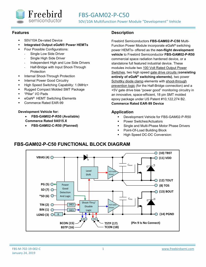
FBS-M-702-19-002-C 1 www.freebirdsemi.com January 24, 2019 FBS-GAM02-P-C50 50V/10A Multifunction Power Module “Development” Vehicle Features 50V/10A De-rated Device Integrated Output eGaN® Power HEMTs Four Possible Configurations: - Single Low Side Driver - Single High Side Driver - Independent High and Low Side Drivers - Half-Bridge with Input Shoot-Through Protection Internal Shoot-Through Protection Internal Power Good Circuitry High Speed Switching Capability: 1.0MHz+ Rugged Compact Molded SMT Package “Pillar” I/O Pads eGaN ® HEMT Switching Elements Commerce Rated EAR-99 Development Vehicle for: • FBS-GAM02-P-R50 (Available) Commerce Rated 9A515.X • FBS-GAM02-C-R50 (Planned) Description Freebird Semiconductors FBS-GAM02-P-C50 Multi- Function Power Module incorporate eGaN ® switching power HEMTs- offered as the non-flight development vehicle to Freebird Semiconductor FBS-GAM02-P-R50 commercial space radiation hardened device, or a standalone full featured industrial device. These modules include two 100 Volt Rated Output Power Switches, two high speed gate drive circuits (consisting entirely of eGaN ® switching elements), two power Schottky diode clamp elements with shoot-through prevention logic (for the Half-Bridge connection) and a +5V gate drive bias “power good” monitoring circuitry in an innovative, space-efficient, 18 pin SMT molded epoxy package under US Patent #10,122,274 B2. Commerce Rated EAR-99 Device Application Development Vehicle for FBS-GAM02-P-R50 Power Switches/Actuators Single and Multi-Phase Motor Phase Drivers Point-Of-Load Building Block High Speed DC-DC Conversion: FBS-GAM02-P-C50 FUNCTIONAL BLOCK DIAGRAM Level Shift (13) BOUT (14) PGND Shoot-Thru/ Disable Logic VBIAS (4) Power Good Detection And Logic PG (5) *SD (6) TIN (2) 1KΩ BIN (1) 1KΩ H/S Gate Driver H/S Gate Driver SD (7) R LGND (3) (Pin 9 Is No Connect) (11) VDD (12) TOUT (8) TOS (10) TBST BSTP (16) BCON (15) TSTP (17) TCON (18) Cboot Cbyp
Transcript of Freebird Semiconductor - FBS-GAM02-P-C50 · 2019-01-31 · FBS-GAM02-P-C50 ©2019 Freebird...
FBS-M-702-19-002-C 1 www.freebirdsemi.com January 24, 2019
FBS-GAM02-P-C50 50V/10A Multifunction Power Module “Development” Vehicle
Features
50V/10A De-rated Device Integrated Output eGaN® Power HEMTs Four Possible Configurations:
- Single Low Side Driver - Single High Side Driver - Independent High and Low Side Drivers - Half-Bridge with Input Shoot-Through
Protection Internal Shoot-Through Protection Internal Power Good Circuitry High Speed Switching Capability: 1.0MHz+ Rugged Compact Molded SMT Package “Pillar” I/O Pads eGaN® HEMT Switching Elements Commerce Rated EAR-99 Development Vehicle for:
• FBS-GAM02-P-R50 (Available) Commerce Rated 9A515.X • FBS-GAM02-C-R50 (Planned)
Description Freebird Semiconductors FBS-GAM02-P-C50 Multi-Function Power Module incorporate eGaN® switching power HEMTs- offered as the non-flight development vehicle to Freebird Semiconductor FBS-GAM02-P-R50 commercial space radiation hardened device, or a standalone full featured industrial device. These modules include two 100 Volt Rated Output Power Switches, two high speed gate drive circuits (consisting entirely of eGaN® switching elements), two power Schottky diode clamp elements with shoot-through prevention logic (for the Half-Bridge connection) and a +5V gate drive bias “power good” monitoring circuitry in an innovative, space-efficient, 18 pin SMT molded epoxy package under US Patent #10,122,274 B2. Commerce Rated EAR-99 Device
Application Development Vehicle for FBS-GAM02-P-R50 Power Switches/Actuators Single and Multi-Phase Motor Phase Drivers Point-Of-Load Building Block High Speed DC-DC Conversion:
FBS-GAM02-P-C50 FUNCTIONAL BLOCK DIAGRAM
Level Shift
(13) BOUT
(14) PGND
Shoot-Thru/ Disable Logic
VBIAS (4)
Power Good
Detection And Logic
PG (5)
*SD (6)
TIN (2) 1KΩ
BIN (1) 1KΩ
H/S Gate Driver
H/S Gate Driver
SD (7)
R LGND (3)
(Pin 9 Is No Connect)
(11) VDD
(12) TOUT (8) TOS
(10) TBST
BSTP (16) BCON (15) TSTP (17)
TCON (18)
Cboot
Cbyp

FBS-GAM02-P-C50
©2019 Freebird Semiconductor Corporation Page 2 of 45 www.freebirdsemi.com
FBS-GAM02-P-C50 CONFIGURATION AND PIN ASSIGNMENTS
FBS-GAM02-P-C50 CONFIGURATION AND PIN ASSIGNMENT TABLE
Pin # Pin Name Input/Output Pin Function 1 BIN I Low-Side Switch Logic Input 2 TIN I High-Side Switch Logic Input 3 LGND -- Logic Ground, 0V (Low Current) 4 VBIAS I +5V Gate Driver Power Supply Bias Input Voltage 5 PG O Power Good Logic Output (Open Drain) 6 *SD I Low True Shutdown Input 7 SD I High True Shutdown Input 8 TOS I High-Side Output (Switching Node) Sense 9 N/C -- No Internal Connection
10 TBST I High-Side Bootstrap Potential 11 VDD I Positive Power Input Supply Voltage (High Current) 12 TOUT O High-Side Output, High Side Switch (High Current) 13 BOUT O Low-Side Output, Low Side Switch (High Current) 14 PGND -- Power Supply Return, 0V (High Current) 15 BCON I Low-Side Switch Shoot Through Control Input 16 BSTP O Low-Side Switch Shoot Through Protection Output 17 TSTP O High-Side Switch Shoot Through Protection Output 18 TCON I High-Side Switch Shoot Through Control Input
18 Pin Molded SMT Package w/Pillar Pins
1
2
3
4
5
6 7 8 9 10 11
12
13
14 15 16 17 18
TOP (X-Ray) VIEW BOTTOM (Pad) VIEW
1
2
6 7 8 9 10 11
12
13
14
5
4
3
18 17 16 15

FBS-GAM02-P-C50
©2019 Freebird Semiconductor Corporation Page 3 of 45 www.freebirdsemi.com
Absolute Maximum Ratings -40oC≤ TC ≤ 85oC unless otherwise noted.
Symbol Parameter-Conditions Value Units
VDS Power Switch Drain to Source Voltage: (Note 1) 50% Voltage De-Rating 50
V No Voltage De-Rating 100
V(BEMF) Half-Bridge-Connected BEMF Voltage at BOUT/TOUT Terminals: Motor Driver Coast Mode, Three Phase Voltage/Phase-to-Phase (Note 20) 20 Vpk
ID Continuous Drain Current 10 A VBIAS Continuous Gate Driver Bias Supply Voltage -0.3 to 6.0 V BIN,TIN BIN or TIN Input Voltage -0.3 to 5.5 V TSTG Storage Junction Temperature Range -55 to +140 oC TJ Operating Junction Temperature Range -45 to +110 oC Tc Case Operating Temperature Range -40 to +85 oC Tsol Package Mounting Surface Temperature 230 oC
ESD ESD class level (HBM) 1A
Thermal Characteristics
Symbol Parameter-Conditions Value Units RθJC Thermal Resistance Junction to Case, Either eGaN® Power Switch (Note 3) 8.5 oC/W RθJC Thermal Resistance Junction to Case, Either Clamp Schottky Diode (Note 3) 20

FBS-GAM02-P-C50
©2019 Freebird Semiconductor Corporation Page 4 of 45 www.freebirdsemi.com
Low- and High-Side Power Switch Static Electrical Characteristics TC =25oC unless otherwise noted.
PARAMETER SYMBOL TEST CONDITIONS MIN TYP MAX UNITS
Drain - Source Leakage Current IDSS
VDS = 25V; BIN = TIN = 0.8Vdc (Note 1)
Tc= 25oC - 10 125
uA
Tc= 85oC - 125 450
VDS = 50V; BIN = TIN = 0.8Vdc (Note 1)
Tc= 25oC - 25 170 Tc= 85oC - 170 705
VDS = 100V; BIN = TIN =0.8Vdc (Note 1)
Tc= 25oC - 95 Tc= 85oC - 550
Half-Bridge-Connected Back-EMF (BEMF) Leakage Current: Motor Driver Coast-Mode
IBEMF BEMF = 15Vpk BIN = TIN = 0.8Vdc (Notes 10, 12, 20)
Tc= 25oC 60 mApk
Drain - Source ON-State Resistance RDS(ΟΝ) ID = 10A (Note 2) Tc= 25oC 7 10
mΩ Tc= 85oC - 10 15 Tc= -40oC 5.5 8
Source-Drain Clamping Voltage VSD ID = -10A (Note 2) Tc= 25oC 0.90 0.97
V Tc= 85oC 0.83 0.90 Tc= -40oC 0.97 1.15
BIN, TIN Logic Input Static Electrical Characteristics -40oC≤ TC ≤ +85oC unless otherwise noted.
PARAMETER SYMBOL TEST CONDITIONS MIN TYP MAX UNITS
Low Logic Level Input Voltage VIL VBIAS = 5.0Vdc (Note 4) 0.8 V High Logic Level Input Voltage VIH VBIAS = 5.0Vdc (Note 5) 2.9 V
Low Logic Level Input Current IIL VBIAS = 5.0V, VIL = 0.4V Tc= 25oC -5 +/-1 5
uA Tc= 85oC -50 +/-
10 50
High Logic Level Input Current IIH VBIAS = 5.0V, VIH = 3.0V Tc= 25oC -5 +/-1 5
uA Tc= 85oC -50 +/-
10 50
High Logic Level Shoot-Through-State Logic Input Current IIHST
VBIAS < UVLO- or VBIAS > OVLO+ BIN = TIN = 3.0Vdc
Tc = 25oC 3 mA
PG Logic Output Static Electrical Characteristics -40oC≤ TC ≤ 85oC unless otherwise noted.
PARAMETER SYMBOL TEST CONDITIONS MIN TYP MAX UNITS
Low Logic Level Output Voltage VOL VBIAS = 5.0Vdc (Notes 6,7) 0.2 V High Logic Level Output Voltage VOH VBIAS = 5.0Vdc (Note 6,7) 3.5 V Low Logic Level Output Current IOL VBIAS = 5.0V (Note 8) 5 mA High Logic Level Output Leakage Current IOH VBIAS = 5.0V, PG = 5.5V (Note 8) 100 uA
VDD-to-PGND Static Electrical Characteristics -40oC≤ TC ≤ 85oC unless otherwise noted.
PARAMETER SYMBOL TEST CONDITIONS MIN TYP MAX UNITS VDD-to-PGND Operating Voltage Range
VDD-PGND (Note 3) 10 50 V
VBIAS Static Electrical Characteristics -40oC≤ TC ≤ +85oC unless otherwise noted.
PARAMETER SYMBOL TEST CONDITIONS MIN TYP MAX UNITS VBIAS Recommended Operating Voltage Range VBIAS VBIAS = 5.0Vdc (Note 9) 4.75 5.05 5.5 V
VBIAS Operating Current IBIAS VBIAS = 5.5Vdc 16 20 mA
FBS-GAM02-P-C50
©2019 Freebird Semiconductor Corporation Page 5 of 45 www.freebirdsemi.com
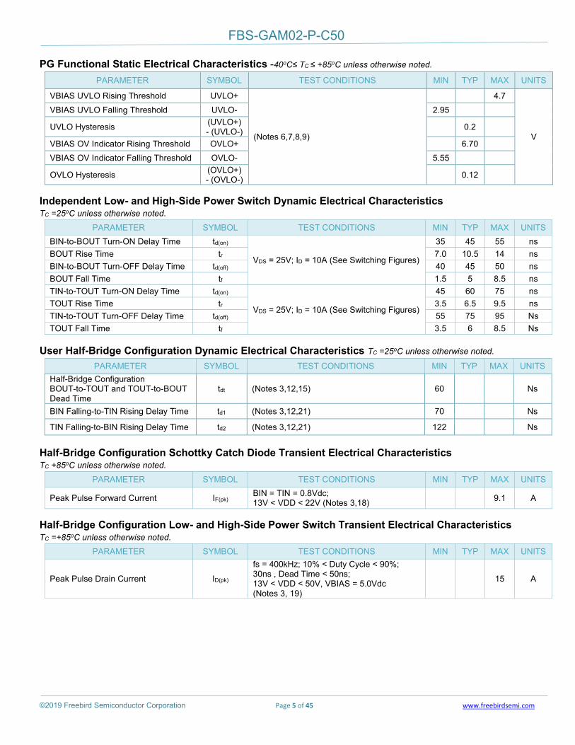
PG Functional Static Electrical Characteristics -40oC≤ TC ≤ +85oC unless otherwise noted.
PARAMETER SYMBOL TEST CONDITIONS MIN TYP MAX UNITS
VBIAS UVLO Rising Threshold UVLO+
(Notes 6,7,8,9)
4.7
V
VBIAS UVLO Falling Threshold UVLO- 2.95
UVLO Hysteresis (UVLO+) - (UVLO-) 0.2
VBIAS OV Indicator Rising Threshold OVLO+ 6.70 VBIAS OV Indicator Falling Threshold OVLO- 5.55
OVLO Hysteresis (OVLO+) - (OVLO-) 0.12
Independent Low- and High-Side Power Switch Dynamic Electrical Characteristics TC =25oC unless otherwise noted.
PARAMETER SYMBOL TEST CONDITIONS MIN TYP MAX UNITS BIN-to-BOUT Turn-ON Delay Time td(on)
VDS = 25V; ID = 10A (See Switching Figures)
35 45 55 ns BOUT Rise Time tr 7.0 10.5 14 ns BIN-to-BOUT Turn-OFF Delay Time td(off) 40 45 50 ns BOUT Fall Time tf 1.5 5 8.5 ns TIN-to-TOUT Turn-ON Delay Time td(on)
VDS = 25V; ID = 10A (See Switching Figures)
45 60 75 ns TOUT Rise Time tr 3.5 6.5 9.5 ns TIN-to-TOUT Turn-OFF Delay Time td(off) 55 75 95 Ns TOUT Fall Time tf 3.5 6 8.5 Ns
User Half-Bridge Configuration Dynamic Electrical Characteristics TC =25oC unless otherwise noted.
PARAMETER SYMBOL TEST CONDITIONS MIN TYP MAX UNITS Half-Bridge Configuration BOUT-to-TOUT and TOUT-to-BOUT Dead Time
tdt (Notes 3,12,15) 60 Ns
BIN Falling-to-TIN Rising Delay Time td1 (Notes 3,12,21) 70 Ns
TIN Falling-to-BIN Rising Delay Time td2 (Notes 3,12,21) 122 Ns Half-Bridge Configuration Schottky Catch Diode Transient Electrical Characteristics TC +85oC unless otherwise noted.
PARAMETER SYMBOL TEST CONDITIONS MIN TYP MAX UNITS
Peak Pulse Forward Current IF(pk) BIN = TIN = 0.8Vdc; 13V < VDD < 22V (Notes 3,18) 9.1 A
Half-Bridge Configuration Low- and High-Side Power Switch Transient Electrical Characteristics TC =+85oC unless otherwise noted.
PARAMETER SYMBOL TEST CONDITIONS MIN TYP MAX UNITS
Peak Pulse Drain Current ID(pk)
fs = 400kHz; 10% < Duty Cycle < 90%; 30ns , Dead Time < 50ns; 13V < VDD < 50V, VBIAS = 5.0Vdc (Notes 3, 19)
15 A

FBS-GAM02-P-C50
©2019 Freebird Semiconductor Corporation Page 6 of 45 www.freebirdsemi.com
Module Dynamic Electrical Characteristics TC =25oC unless otherwise noted. PARAMETER SYMBOL TEST CONDITIONS MIN TYP MAX UNITS
Power Switch Output Capacitance Coss BOUT-PGND or VDD-TOUT = 5Vdc 1150
pF BOUT-PGND or VDD-TOUT = 50Vdc 500
Dynamic Gate/Driver Losses (Per Driver; Low- or High-Side) PGD VBIAS = 5.0Vdc 21 mW/MHz
Internal Bootstrap Capacitance Cboot 47 nF
External Bootstrap Capacitance Cboot(ext) TBST (Pin 10) to TOS (Pin 8) 1.0 uF
LGND-PGND Resistance RG 1.0 Ω High-side Power Switch Start Up Pre-Charge Time: Half Bridge Configuration
tprg (Notes 3,10,11,12)
5 Us
High-side Power Switch Maximum Duty Cycle td/c 95 %
Minimum Switching Frequency: Low-side Power Switch
fs (Notes 3,10,11,12,13,14,15,16)
0 Hz
Minimum Switching Frequency: High-side Power Switch 200 kHz
Maximum Switching Frequency: Half-Bridge Configuration 1.0 TBD MHz
Shoot-Through Protection Activation Delay Time tst (Notes 3,14) 5 Ns
SPECIFICATION NOTES: 1.) VBIAS = +5Vdc, PGND = LGND = 0V, VDS = VDD-to-TOUT or VDS = BOUT-to-PGND as specified.
2.) Measured using 4-Wire (Kelvin) sensing techniques. 3.) Guaranteed by design. Not tested in production. 4.) When either logic input (BIN or TIN) is at the low input voltage level the associated output (BOUT or TOUT) is
guaranteed to be OFF (high impedance). 5.) When either logic input (BIN or TIN) is at the high input voltage level the associated output (BOUT or TOUT) is
guaranteed to be ON (low impedance).
6.) Parameter measured with a 4.7kΩ pull-up resistor between PG and VBIAS. 7.) PG is at a low level when VBIAS is below the UVLO- (falling) threshold level or the OVLO+ (rising) threshold
level. PG is at a high level when VBIAS is above the UVLO+ (rising) threshold level or the OVLO- (falling) threshold level.
8.) PG is an open drain output referenced to LGND. 9.) VBIAS levels below the UVLO- and above the OVLO+ thresholds result in the internal low-side and high-side
gate drivers being disabled: The logic inputs to the drivers are internally set to a logic low state to prevent damage to the eGaN® power switches.
10.) The high-side power switch gate driver utilizes a bootstrap capacitor to provide the proper bias for this circuit. As such, this capacitor MUST be periodically re-charged from the VBIAS supply. As a stand-alone high-side switch with a ground-connected/ground-sensed load, this recharging takes place each time the switch is turned OFF and the TOUT node returns to ground potential (0Vdc). However, when connected in conjunction with the low-side power switch in the half-bridge configuration, this connection to ground does not exist until the low-side power switch is turned ON, thus creating a low impedance connection from TOUT through the low-side power switch (BOUT-PGND). The time tprg is the minimum time required to ensure that the bootstrap capacitor is properly charged when power is initially applied to the FBS-GAM02-P-C50 Module.
11.) The minimum frequency of operation is determined by the internal bootstrap capacitance and the bias current required by the high-side power switch gate driver circuit. In order to keep the high-side power switch gate driver bootstrap capacitor properly charged it is recommended that the maximum duty cycle (ton * fs) of the high-side power switch is limited to the value shown. Accordingly, the high-side power switch is unsuitable for DC applications with the use of an external DC power supply connected between the TBST(+) and TOS(-) pins.

FBS-GAM02-P-C50
©2019 Freebird Semiconductor Corporation Page 7 of 45 www.freebirdsemi.com
SPECIFICATION NOTES (Cont.):
12.) For half-bridge applications, a “dead” time delay MUST be added between the time when the BOUT output transitions ON-TO-OFF and the TOUT output transitions OFF-to-ON, and also when the TOUT output transitions ON-to-OFF and the BOUT output transitions OFF-to-ON, to avoid both power switches being actuated simultaneously. Simultaneous actuation of the high-side and low-side power switches causes very large, uncontrolled and destructive currents to flow through the ON-state switches from VDD to PGND. In order to calculate the desired output dead times (tDEAD), the delay time from BIN transitioning from logic 1-to-0 to TIN transitioning from logic 0-to-1 is:
td1 = (tLSd(OFF) + tLSf) + tDEAD – (tHSd(ON) + tHSr),
where the LS nomenclature refers to the low-side driver off-delay and fall times and the HS nomenclature refers to the high-side driver on-delay time and rise time.
The delay time from TIN transitioning from logic 1-to-0 to BIN transitioning from logic 0-to-1 is:
td2 = (tHSd(OFF) + tHSf) + tDEAD – (tLSd(ON) + tLSr),
where the HS nomenclature refers to the high-side driver off-delay and fall times and the LS nomenclature refers to the low-side driver on-delay time and rise time.
13.) The maximum dead time prevents the Schottky clamp diodes in the power switch outputs from being overstressed and damaged by excessive power dissipation. The maximum dead time is limited by the switching frequency and by the power dissipation of the Schottky diodes: Pd = Vf * Io * 2 * td/T. Please refer to Figures 27, 28 and 30.
14.) The input shoot-through protection is activated if both the BIN and TIN logic inputs are set to the logic high (“1”) condition simultaneously. In the case where the BIN and TIN inputs are set to logic high, both the low- and high-side power switches are set to their high impedance (OFF) state.
15.) VDD = 50V, ID = +/-10A and fs = 1.0MHz. Half-bridge configuration. 16.) The maximum switching frequency is limited by power dissipation in the half-bridge configuration, and not by
throughput delay times. Faster switching frequencies are possible at reduced Vdd and Io operating levels and at reduced ambient operating temperatures. See Figures 23 through 26.
17.) See Figure 22. 18.) Half-bridge configuration. Current from pin 12 to pin 11 (high-side Schottky) or pin 14 to pin 13 (low-side
Schottky), not drawn simultaneously. Pulse duration = 500us. Repetition rate = 5 seconds. 19.) Half-bridge configuration. Current from pin 11 to pin 12 or pin 12 to pin 11 (High-side Power Switch), or pin 13
to pin 14 or pin 14 to pin 13 (low-side Power Switch), not drawn simultaneously. Pulse duration = 500us. Repetition rate = 5 seconds.
BIN
TIN
td1 td2

FBS-GAM02-P-C50
©2019 Freebird Semiconductor Corporation Page 8 of 45 www.freebirdsemi.com
SPECIFICATION NOTES (Cont.):
20.) When connected in the half-bridge configuration and with a motor load in the coast mode (BIN = TIN = low logic level), the motor back-EMF (BEMF) caused by rotation (generator effect) will cause a “leakage” current to flow into the switching node of the GAM02 module (BOUT/TOUT common connection). This leakage current is due to the high-side driver biasing circuitry. Due to the power ratings of the internal components, the peak value of the BEMF should be limited to that value shown in the Absolute Maximum Ratings. Additionally, when operating in the coast mode, in order to guarantee proper operation of the half-bridge circuit, the high-side driver bootstrap capacitor MUST BE recharged periodically in order to assure that the high-side gate driver is biased properly, and that the high-side power switch responds correctly to the TIN logic input. If the high-side bootstrap capacitor is not periodically recharged, then potentially destructive currents may flow in the GAM02 module.
21.) Setting the BIN-to-TIN and TIN-to-BIN delay times, td1 and td2, to the values shown in the table guarantees shoot-through free operation of the GAM02 module when connected in the half-bridge configuration.
FBS-GAM02-P-C50
©2019 Freebird Semiconductor Corporation Page 9 of 45 www.freebirdsemi.com
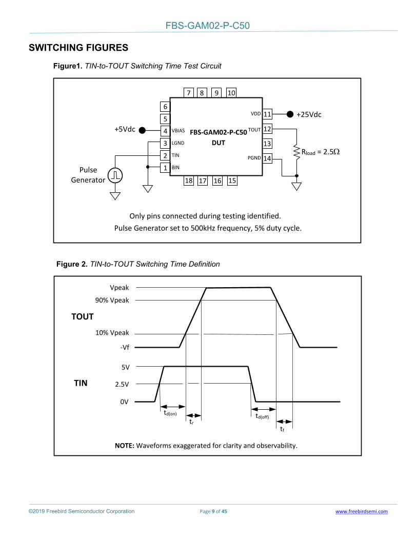
SWITCHING FIGURES
Figure1. TIN-to-TOUT Switching Time Test Circuit
Figure 2. TIN-to-TOUT Switching Time Definition
+25Vdc 11
12
18 17 16 15
14
13
7 8 9 10
3
4
5
6
1
2
+5Vdc FBS-GAM02-P-C50 DUT
Rload = 2.5Ω
Pulse Generator
BIN
TIN
LGND
VBIAS
VDD
TOUT
PGND
Only pins connected during testing identified. Pulse Generator set to 500kHz frequency, 5% duty cycle.
TOUT
TIN
10% Vpeak
5V
0V
2.5V
td(on)
-Vf
90% Vpeak
Vpeak
tr
NOTE: Waveforms exaggerated for clarity and observability.
td(off)
tf

FBS-GAM02-P-C50
©2019 Freebird Semiconductor Corporation Page 10 of 45 www.freebirdsemi.com
SWITCHING FIGURES (Continued.) Figure 3. BIN-to-BOUT Switching Time Test Circuit
Figure 4. BIN-to-BOUT Switching Time Definition
+25Vdc
11
12
18 17 16 15
14
13
7 8 9 10
3
4
5
6
1
2
+5Vdc FBS-GAM02-P-C50 DUT
Rload = 2.5Ω
Pulse Generator
BIN
TIN
LGND
VBIAS
VDD
BOUT
PGND
Only pins connected during testing identified. Pulse Generator set to 500kHz frequency, 5% duty cycle.
BOUT
BIN
10% Vpeak
5V
0V
2.5V
td(on)
Von
90% Vpeak
Vpeak
tr
NOTE: Waveforms exaggerated for clarity and observability.
td(off)
tf

FBS-GAM02-P-C50
©2019 Freebird Semiconductor Corporation Page 11 of 45 www.freebirdsemi.com
SWITCHING FIGURES (Continued.)
Figure 5. VBIAS-to-PG Relationship
VBIAS
PG
UVLO+
VOH
VOL
UVLO-
OVLO- OVLO+
NOTE: Waveforms exaggerated for clarity and observability.
0V

FBS-GAM02-P-C50
©2019 Freebird Semiconductor Corporation Page 12 of 45 www.freebirdsemi.com
TYPICAL APPLICATION INFORMATION
The following figures detail the suggested applications for the FBS-GAM02-P-C50 Module. For all
applications, please refer to the Implementation section, following, for proper power supply bypassing and
layout recommendations and criteria. In any of the following applications, if an inductive load is driven then
an appropriately-rated Schottky rectifier/diode should be connected across the load to prevent destructive
flyback/”kickback” voltages from destroying the FBS-GAM02-P-C50.
In all the following figures only the pins that are considered or that require connection are identified.
Figure 6. Single High-Side Power Switch Configuration
Figure 7. Single Low-Side Power Switch Configuration
VDD 11
12
18 17 16 15
14
13
7 8 9 10
3
4
5
6
1
2
+5Vdc FBS-GAM02-P-C50
Rload
BIN
TIN
LGND
VBIAS
VDD
TOUT
PGND PWM In
VDD
11
12
18 17 16 15
14
13
7 8 9 10
3
4
5
6
1
2
+5Vdc FBS-GAM02-P-C50
Rload
BIN
TIN
LGND
VBIAS
VDD
BOUT
PGND PWM In

FBS-GAM02-P-C50
©2019 Freebird Semiconductor Corporation Page 13 of 45 www.freebirdsemi.com
Figure 8. Independent High- and Low-Side Power Switches
Figure 9. Independent Switch Configuration: Two-Transistor Forward Converter Output Stage
VDD
11
12
18 17 16 15
14
13
7 8 9 10
3
4
5
6
1
2
+5Vdc FBS-GAM02-P-C50
Rload1
BIN
TIN
LGND
VBIAS
VDD
BOUT
PGND PWM1 In Rload2
TOUT
PWM2 In
VDD
11
12
18 17 16 15
14
13
7 8 9 10
3
4
5
6
1
2
+5Vdc FBS-GAM02-P-C50 Rload
BIN
TIN
LGND
VBIAS
VDD
BOUT
PGND PWM In
TOUT
L
T
C
D1
D2 D3
D4
N:1
VOUT
T
ton
PWM
VOUT = (VDD • ton)/(N • T)

FBS-GAM02-P-C50
©2019 Freebird Semiconductor Corporation Page 14 of 45 www.freebirdsemi.com
Figure 10. Half-Bridge Configuration: POL Converter Output Stage
VDD
11
12
18 17 16 15
14
13
7 8 9 10
3
4
5
6
1
2
+5Vdc FBS-GAM02-P-C50
Rload BIN
TIN
LGND
VBIAS
VDD
BOUT
PGND PWM1 In
TOUT L
C
VOUT
T
ton
PWM1
VOUT = ~ VDD • (ton/T)
PWM2 In
td td
PWM2
BCO
N
BSTP
TSTP
TCO
N

FBS-GAM02-P-C50
©2019 Freebird Semiconductor Corporation Page 15 of 45 www.freebirdsemi.com
Figure 11. Half-Bridge Configuration: Single Phase Motor Drive Stage
VDD
+5Vd
c
PWM
1 In
M
OTO
R
T
t on
PWM
1 Spee
d Co
ntro
l
PWM
2 In
t d
t d 11 12
18
17
16
15
14 13
7
8
9
10
3 4 5 6 1 2
BIN
TIN
LGN
D
VBIA
S
VDD
BOU
T
PGN
D
TOU
T
PWM
2
Forw
ard
Reve
rse
11 12
18
17
16
15
14 13
7
8
9
10
3 4 5 6 1 2
FBS-
GAM
02-P
-C50
BIN
TIN
LGN
D
VBIA
S
VDD
BOU
T
PGN
D
TOU
T
VDD
+5Vd
c
Dire
ctio
n Co
ntro
l
FBS-
GAM
02-P
-C50
BCON
BSTP
TSTP
TCON
BCON
BSTP
TSTP
TCON

FBS-GAM02-P-C50
©2019 Freebird Semiconductor Corporation Page 16 of 45 www.freebirdsemi.com
Figure 12. Half-Bridge Configuration: Single Phase Motor Driver Equivalent Circuit
VDD
Motor State Truth Table
PWM1 In +
Motor Spins Forward When Polarized + to -.
PWM2 In
MOTOR -
Forward
Reverse
“H” Bridge
Motor Spins Reverse When Polarized - to +.
0 = Switch OFF, 1 = Switch ON, X = Don’t Care, Min D = Minimum Duty Cycle, Max D = Maximum Duty Cycle.
PWM1 PWM2 Forward Reverse Motor Result (Direction/Speed) X X 0 0 OFF/Coast Mode
Min D Max D 1 0 Forward/Max Speed Max D Min D 1 0 Forward/Min Speed Min D Max D 0 1 Reverse/Min Speed Max D Min D 0 1 Reverse/Max Speed
Speed Direction
FBS-GAM02-P-C50
©2019 Freebird Semiconductor Corporation Page 17 of 45 www.freebirdsemi.com
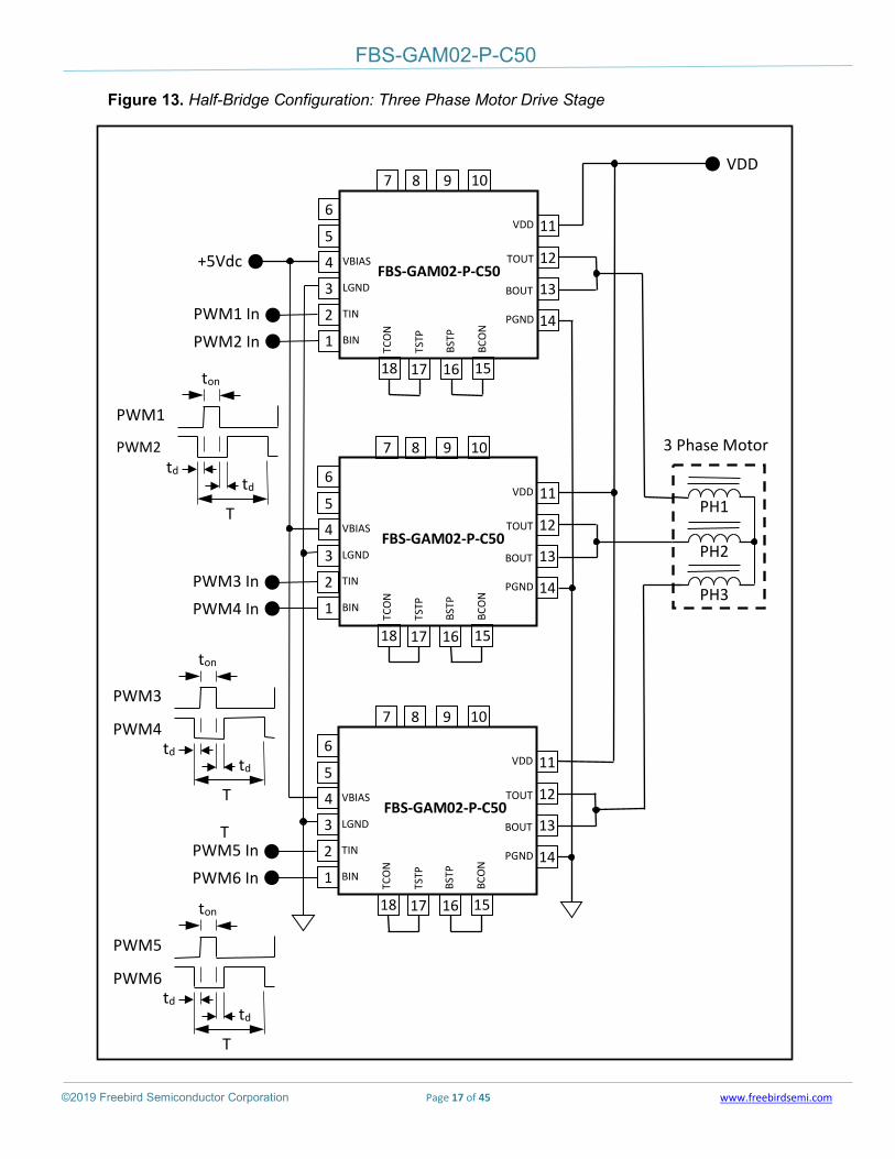
Figure 13. Half-Bridge Configuration: Three Phase Motor Drive Stage
VDD
11
12
18 17 16 15
14
13
7 8 9 10
3
4
5
6
1
2
+5Vdc FBS-GAM02-P-C50
BIN
TIN
LGND
VBIAS
VDD
BOUT
PGND PWM1 In
TOUT
PWM2 In BCO
N
BSTP
TSTP
TCO
N
3 Phase Motor
11
12
18 17 16 15
14
13
7 8 9 10
3
4
5
6
1
2
PH1
FBS-GAM02-P-C50
BIN
TIN
LGND
VBIAS
VDD
BOUT
PGND PWM3 In
TOUT
PWM4 In BCO
N
BSTP
TSTP
TCO
N
11
12
18 17 16 15
14
13
7 8 9 10
3
4
5
6
1
2
FBS-GAM02-P-C50
BIN
TIN
LGND
VBIAS
VDD
BOUT
PGND PWM5 In
TOUT
PWM6 In BCO
N
BSTP
TSTP
TCO
N
PH2
PH3
T
PWM5
td td
PWM6
ton
T
T
PWM1
td td
PWM2
ton
T
PWM3
td td
PWM4
ton

FBS-GAM02-P-C50
©2019 Freebird Semiconductor Corporation Page 18 of 45 www.freebirdsemi.com
INTERFACING THE FBS-GAM02 TO LEGACY RAD-HARD PWM CONTROLLERS
The BIN and TIN logic inputs for the FBS-GAM02-P-C50 have a maximum desired input voltage level limit of
5Vdc due to the requirements of the eGaN HEMT technology utilized in the Module. This may seem to preclude the
use of the GAM02 with legacy rad-hard PWM controllers such as the 182X family -- whose PWM outputs are 12Vdc,
minimum -- due to this logic input voltage limitation. But this is not the case as there are several ways to interface
the GAM02 to these controllers:
a.) Zener diode voltage clamp with dead-time generation circuit.
A Zener diode may be used to clamp the BIN and TIN logic inputs of the FBS-GAM02-P-C50 in order
to interface the module to a high output voltage level PWM controller, as shown in Figure 14. The output
of the UC1823A is a totem-pole configuration, and the output switches between 0V and 12V as logic 0
and logic 1, respectively. The transition times between logic states for a 1000pF load are typically 20ns,
but much faster with lighter loads.
Figure 14. Zener Diode Logic Input Voltage Clamp Circuit and Dead Time Delay Circuit
The nominal voltage of the Zener diode, D4, should be 2.7V if U1 through U3 are 3.0 or 3.3V CMOS
logic, and 4.3V if U1 though U3 are 5.0V CMOS logic. Depending upon the Zener diode chosen, the
junction capacitance can be quite high – in the range of 250 to 500pF. This is far greater than the typical
input capacitance of the GAM02, which is 7pF, and thus must be compensated for. Select capacitor CC,
the speed-up capacitor, to achieve the fastest rise time at the input of U1. Select R1 to limit the
+12Vdc
UC1823A-SP TIN
VC
PGND
OUT
CC
R1
BIN
R2
D1
D2
D3
D4
U1 U2
U3
RD1 CD1
CD2 RD2

FBS-GAM02-P-C50
©2019 Freebird Semiconductor Corporation Page 19 of 45 www.freebirdsemi.com
minimum current through Zener D4 to be the nominal Zener current. Select R2 to limit the peak Zener
current to less than the Zener peak current rating. Schottky diodes D1 through D3 are types RB751S40 or
equivalent. Logic gates U1 and U2 are high-speed buffers, preferably with Schmitt-trigger inputs and
logic gate U3 is a high-speed inverter, again preferably with Schmitt-trigger input. These three logic
gates, along with resistors RD1 and RD2 and capacitors CD1 and CD2 form the dead-time circuit required
for the GAM02 when it is connected in the half-bridge configuration, such as for the power output stage
of a POL DC-DC converter. In the circuit, resistor RD1 and capacitor CD1 implement the time delay td1 and
RD2 and CD2 implement the time delay td2 (see Notes 12 and 21). Set RD1 and RD2 to 1KΩ and then
select CD1 and CD2 to obtain time delays tD1 and tD2 as shown in the “Half-Bridge Configuration Dynamic
Electrical Characteristics” parametric table on page 5. All component values and performance criteria
should be verified with simulation modeling.
b.) Zener diode voltage clamp with ASIC/FPGA Two-Phase PWM Generator.
The same Zener diode clamping circuit as shown in Figure 14 may be used to clamp the output of the
UC1823A to a lower voltage level in order to present it to an ASIC/FPGA in order to generate the
requisite two-phase clock signals for the BIN and TIN logic inputs of the FBS-GAM02-P-C50. A typical
circuit for this circuit implementation is shown in Figure 15:
Figure 15. Zener Diode Logic Input Voltage Clamp Circuit With ASIC/FPGA Two-Phase Clock
(With Dead Time) Generator
In the circuit of Figure 15 all the high-speed and high accuracy analog functions associated with the PWM
controller are performed off-chip from the FPGA/ASIC. The programmable logic of the FPGA/ASIC and the
associated firmware code is responsible for generating the two-phase clock with dead times required by the
BIN and TIN inputs of the FBS-GAM02-P-C50
+12Vdc
UC1823A-SP
TIN VC
PGND
OUT
CC
R1
BIN
R2
D1
D4
FPGA/ ASIC
GPI
GPO1
GPO2

FBS-GAM02-P-C50
©2019 Freebird Semiconductor Corporation Page 20 of 45 www.freebirdsemi.com
Adaptive Dead Time Control For the FBS-GAM02-P-C50
In circuits shown in both Figure 14 and 15 the dead times required by the FBS-GAM02-P-C50 to avoid cross-
conduction/shoot-through are generated in a “brute force” manner either with analog components (Figure 14) or
with programmable logic and firmware in an FPGA/ASIC (Figure 15). There is another way to obtain the optimum
dead times for the FBS-GAM02-P-C50 device – adaptive dead time control, as shown in Figure 16.
Figure 16. Adaptive Dead Time Control for Cross-Conduction/Shoot-Through Avoidance
Adaptive dead time control utilizes the state of the switching node (SN) of the GAM02 in order to allow the
BIN or TIN signals (in this case the BIN signal is the simple logical inverse of the TIN signal) to be applied to the BIN or
TIN logic inputs of the FBS-GAM02P-C50 in order to avoid dynamic cross-conduction/shoot-though in the low- and
high-side output power HEMTs. If the switching node of the FBS-GAM02-P-C50 is “low” (i.e. at PGND) then the low-
side switch is turned ON, or in the process of turning OFF, and the high-side switch must not be turned ON (i.e. a
logic 1 applied to the TIN input). Similarly, if the switching node is “high” (i.e. at VDD), then the-high side switch is
turned ON, or in the process of turning OFF, and the low-side switch must not be turned ON (i.e. a logic 1 applied to
the BIN input). However, if the BIN input is logic 0 and the switching node is “high” (i.e. the high-side catch Schottky
conducting load current) then the TIN input may be set to logic 1 to turn on the high-side driver. This same situation
applies to the high-side driver: If the TIN input is logic 0 and the switching node is “low” (i.e. the low-side catch
Schottky is conducting load current) then the BIN input may be set to logic 1 to turn on the low-side driver. The
circuit shown in Figure 16 relies on a similar voltage clamping scheme for the switching node as was utilized in
Figures 14 and 15, with the exception that the power supply VDD, and subsequent range of the switching node, could
TIN
BIN U3
U3
CC
R1
R3
D1
D2 R2
From GAM02 Half-Bridge
Switching Node
PWM Signal: From FPGA/ASIC
or PWM Controller

FBS-GAM02-P-C50
©2019 Freebird Semiconductor Corporation Page 21 of 45 www.freebirdsemi.com
be much higher than 12V – in fact up to 50V for the FBS-GAM02-P-C50. So greater care must be exercised in the
selection of the clamping components to avoid excessive power dissipation in them, and the associated decrease in
circuit efficiency. It is strongly recommended to simulate the circuit once the components have been selected to
ensure that the proper clamping level is achieved and that the power dissipation of the clamp circuit is kept to a
reasonable level so as not to affect overall circuit operating efficiency.
The key objective in the application of the adaptive dead time control circuit is to minimize the time delay
associated with the voltage clamping circuit. Ideally, the desired time delay of the clamping circuit is zero in order to
achieve the lowest (optimum) dead times. However, some delay is expected because the Zener diode clamp has
finite capacitance and the biasing/current limiting delay resistors contribute an R1-Czener inherent delay. There are
certainly other methods to level-shift and monitor the switching node so as to ascertain its voltage level/state. Again,
the key is to determine that state as quickly as possible so that switching decisions may be made at the BIN and TIN
inputs of the FBS-GAM02-P-C50 as quickly as possible.

FBS-GAM02-P-C50
©2019 Freebird Semiconductor Corporation Page 22 of 45 www.freebirdsemi.com
PIN DETAILS
BIN (Pin 1) The BIN pin is the logic input for low-side power driver. When the BIN input pin is logic low (“0”), the low-
side output (BOUT-PGND) pins (pins 13 and 14) are in the OFF (high-impedance) state. When the BIN input pin is
logic high (“1”), the BOUT-PGND pins are in the ON (low impedance) state.
TIN (Pin 2) The TIN pin is the logic input for high-side power driver. When the TIN input pin is logic low (“0”), the High-
side output (VDD-TOUT) pins (pins 11 and 12) are in the OFF (high impedance) state. When the TIN input pin is logic
high (“1”), the VDD-TOUT pins are in the ON (low impedance) state.
LGND (Logic Ground) (Pin 3) For proper operation of the FBS-GAM02-P-C50, the LGND pin (Pin 3) MUST be connected directly to the
system logic ground return in the application circuit.
VBIAS (Pin 4) The VBIAS pin is the raw input DC power input for the FBS-GAM02-P-C50 module. It is recommended that a
1.0 microfarad ceramic capacitor and a 0.1microfarad ceramic capacitor, each 25V rating, be connected between
VBIAS (pin 4) and system power ground plane (the common tie point of PGND1 and the ground plane) to obtain the
specified switching performance.
PG (Power Good) (Pin 5) The PG pin is an open drain logic-compatible output. For proper operation the PG pin must be pulled-up to
VBIAS, external to the module, with a 4.7kΩ resistor.
The FBS-GAM02-P-C50 incorporates a Power Good (PG) sensing circuit that disables both the low- and high-
side internal gate drivers when the +5V gate drive bias potential (VBIAS) falls below an under-voltage threshold,
typically 4.45V, or rises above a potentially-damaging VBIAS over-voltage threshold level – refer to Figure 5 for the
proper operational nomenclature and functionality versus the state of the VBIAS power supply. During the time
when the VBIAS potential is outside of the pre-set threshold(s), the PG output (Pin 5) pin is logic low (“0”).
Alternatively, when the VBIAS potential is within the pre-set thresholds the PG pin is logic high (“1”). The logic
condition of the PG pin may be sensed by a rad hard FPGA or Microcontroller/DSP in-order to determine when the
power switches in the FBS-GAM02-P-C50 may be driven with a pulse-width modulated (PWM) input signal(s) at the
BIN and TIN logic inputs. If either the under-voltage and over-voltage indication features are not required or desired,
then these functions may be disabled separately by connecting the *SD (Pin 6) pin to VBIAS (pin 4) for the UVLO or
the SD pin (Pin 7) to LGND (pin 3) for the OV indicator, as shown in Figure 17.
FBS-GAM02-P-C50
©2019 Freebird Semiconductor Corporation Page 23 of 45 www.freebirdsemi.com
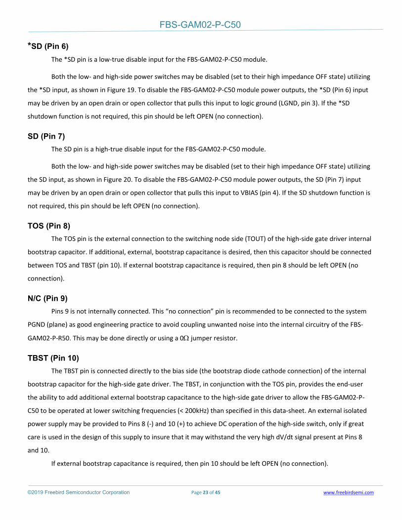
*SD (Pin 6) The *SD pin is a low-true disable input for the FBS-GAM02-P-C50 module.
Both the low- and high-side power switches may be disabled (set to their high impedance OFF state) utilizing
the *SD input, as shown in Figure 19. To disable the FBS-GAM02-P-C50 module power outputs, the *SD (Pin 6) input
may be driven by an open drain or open collector that pulls this input to logic ground (LGND, pin 3). If the *SD
shutdown function is not required, this pin should be left OPEN (no connection).
SD (Pin 7) The SD pin is a high-true disable input for the FBS-GAM02-P-C50 module.
Both the low- and high-side power switches may be disabled (set to their high impedance OFF state) utilizing
the SD input, as shown in Figure 20. To disable the FBS-GAM02-P-C50 module power outputs, the SD (Pin 7) input
may be driven by an open drain or open collector that pulls this input to VBIAS (pin 4). If the SD shutdown function is
not required, this pin should be left OPEN (no connection).
TOS (Pin 8) The TOS pin is the external connection to the switching node side (TOUT) of the high-side gate driver internal
bootstrap capacitor. If additional, external, bootstrap capacitance is desired, then this capacitor should be connected
between TOS and TBST (pin 10). If external bootstrap capacitance is required, then pin 8 should be left OPEN (no
connection).
N/C (Pin 9) Pins 9 is not internally connected. This “no connection” pin is recommended to be connected to the system
PGND (plane) as good engineering practice to avoid coupling unwanted noise into the internal circuitry of the FBS-
GAM02-P-R50. This may be done directly or using a 0Ω jumper resistor.
TBST (Pin 10) The TBST pin is connected directly to the bias side (the bootstrap diode cathode connection) of the internal
bootstrap capacitor for the high-side gate driver. The TBST, in conjunction with the TOS pin, provides the end-user
the ability to add additional external bootstrap capacitance to the high-side gate driver to allow the FBS-GAM02-P-
C50 to be operated at lower switching frequencies (< 200kHz) than specified in this data-sheet. An external isolated
power supply may be provided to Pins 8 (-) and 10 (+) to achieve DC operation of the high-side switch, only if great
care is used in the design of this supply to insure that it may withstand the very high dV/dt signal present at Pins 8
and 10.
If external bootstrap capacitance is required, then pin 10 should be left OPEN (no connection).

FBS-GAM02-P-C50
©2019 Freebird Semiconductor Corporation Page 24 of 45 www.freebirdsemi.com
VDD (Pin 11) The VDD pin (pin 11) is the high current reference (open drain) pin for the internal power eGaN HEMT
associated with high-side power driver. This pin should be connected directly to the system power (VDD) bus via a
low impedance connection, preferably through a low impedance power plane. This pin should be properly bypassed
to the system power ground (PGND) using the guidelines found in the “Recommended VDD-to-PGND Power Supply
Bypassing” section, following.
TOUT (Pin 12) The TOUT pin (pin 12) is the high-current output pin for the high-side driver in the FBS-GAM02-P-C50
module. This pin should be connected directly, via a low impedance connection, to the external load in high-side
switch applications or to the BOUT pin (pin 11), and the load, in half-bridge configurations. The internal high-side
gate driver circuitry is referenced to the TOUT pin, which is internally connected to the TOS pin (pin 8).
This is a VERY high dV/dt and dI/dt pin and regardless of the switch configuration the connection to the
external load should be as short as possible to minimize radiated EMI.
BOUT (Pin 13) The BOUT pin (pin 13) is the high current output (open drain) pin for the internal power eGaN HEMT
associated with the low-side power driver. This pin should be connected directly, via a low impedance connection, to
the external load in low-side switch applications or to the TOUT pin (pin 12), and the load, in half-bridge
configurations.
This is a VERY high dV/dt and dI/dt pin and the connection to the external load should be as short as possible
to minimize radiated EMI.
PGND (Pin 14) The PGND pin (pin 14) is the ground return (source) connection for the internal power circuitry eGaN HEMT
and high-speed gate driver circuitry associated with low-side power driver and for the power good and interface logic
for the high-side driver. This pin should be connected directly to the system power return/ground plane to minimize
common source inductance, and the voltage transients associated with this inductance. If load current sensing is
required in the half-bridge configuration, this should be accomplished via a current sense transformer in series with
the drain of the low-side power HEMT (pin 13).
BCON (Pin 15) The BCON pin is the logic input for the input shoot-through protection for low-side power driver. The state of
this pin follows the state of the TIN logic input pin. If input shoot-through protection is desired in the half-bridge

FBS-GAM02-P-C50
©2019 Freebird Semiconductor Corporation Page 25 of 45 www.freebirdsemi.com
configuration where both power drivers (low and high) must not be turned on simultaneously if the BIN and TIN logic
inputs are simultaneously at logic “1”, then BCON (pin 15) should be externally connected to BSTP (pin 16). If no
shoot-through protection is desired, then pin 15 should be left OPEN (no connection).
BSTP (Pin 16) The BSTP pin is the open drain output for the input shoot-through protection for low-side power driver. The
state of this pin is the logical inverse of the BIN logic input pin. If input shoot-through protection is desired in the
half-bridge configuration where both power drivers (low and high) must not be turned on simultaneously if the BIN
and TIN logic inputs are simultaneously at logic “1”, then BSTP (pin 16) should be externally connected to BCON (pin
15). If no shoot-through protection is desired, then pin 16 should be left OPEN (no connection).
TSTP (Pin 17) The TSTP pin is the open drain output for the input shoot-through protection for high-side power driver. The
state of this pin is the logical inverse of the TIN logic input pin. If input shoot-through protection is desired in the half-
bridge configuration where both power drivers (low and high) must not be turned on simultaneously if the BIN and
TIN logic inputs are simultaneously at logic “1”, then TSTP (pin 17) should be externally connected to TCON (pin 18).
If no shoot-through protection is desired, then pin 17 should be left OPEN (no connection).
TCON (Pin 18) The TCON pin is the logic input for the input shoot-through protection for high-side power driver. The state
of this pin follows the state of the BIN logic input pin. If input shoot-through protection is desired in the half-bridge
configuration where both power drivers (low and high) must not be turned on simultaneously if the BIN and TIN logic
inputs are simultaneously at logic “1”, then TCON (pin 18) should be externally connected to TSTP (pin 17). If no
shoot-through protection is desired, then pin 18 should be left OPEN (no connection).

FBS-GAM02-P-C50
©2019 Freebird Semiconductor Corporation Page 26 of 45 www.freebirdsemi.com
Figure 17. PG Protection Functions Disabled
Figure 18. Shoot-Through Protection Function Enabled
11
12
18 17 16 15
14
13
7 8 9 10
3
4
5
6
1
2
+5Vdc FBS-GAM02-P-C50
BIN
TIN
LGND
VBIAS
VDD
BOUT
PGND PWM1 In
TOUT
PWM2 In
*SD SD
11
12
18 17 16 15
14
13
7 8 9 10
3
4
5
6
1
2
+5Vdc FBS-GAM02-P-C50
BIN
TIN
LGND
VBIAS
VDD
BOUT
PGND PWM1 In
TOUT
PWM2 In
FBS-GAM02-P-C50
©2019 Freebird Semiconductor Corporation Page 27 of 45 www.freebirdsemi.com
Figure 19. *SD Input Function Enabled
Figure 20. SD Input Function Enabled
11
12
18 17 16 15
14
13
7 8 9 10
3
4
5
6
1
2 Q
FBS-GAM02-P-C50
BIN
TIN
LGND
VBIAS
VDD
BOUT
PGND PWM1 In
TOUT
PWM2 In
*SD
R SD
+5Vdc
11
12
18 17 16 15
14
13
7 8 9 10
3
4
5
6
1
2
Q
FBS-GAM02-P-C50
BIN
TIN
LGND
VBIAS
VDD
BOUT
PGND PWM1 In
TOUT
PWM2 In
SD R *SD
+5Vdc

FBS-GAM02-P-C50
©2019 Freebird Semiconductor Corporation Page 28 of 45 www.freebirdsemi.com
HIGH-SIDE BOOTSTRAP CAPACITOR PERIODIC RECHARGE
The high-side power switch gate driver utilizes a bootstrap capacitor to provide the proper bias for this
circuit during switching operation. As such, this capacitor MUST be periodically re-charged from the VBIAS power
supply. As a stand-alone high-side switch with a ground-connected/ground-sensed load, this recharging takes
place each time the switch is turned OFF and the TOUT node returns to ground potential (0Vdc). However, when
connected in conjunction with the low-side power switch in the Half-Bridge configuration (See Figure 10, for
example), this connection to ground does not exist until the low-side power switch is turned ON, thus creating a
low impedance connection from TOUT through the low-side power switch (BOUT-PGND). If the high-side gate
driver is not provided with periodic recharge during operation, damage may occur to the Module.
The time tprg is the minimum time required for the low-side driver to be turned ON in order to ensure that
the bootstrap capacitor is properly charged when power is initially applied to the FBS-GAM02-P-C50 Module.
If DC operation is desired for the Module when connected as two single, independent, power drivers (see
Figures 6, 7 or 8, for examples) then an isolated +4.75 to +5.5Vdc power supply capable of operation with high
rates-of-change of voltage from primary-to-secondary should be connected to the TBST (pin 10) and TOS (pin 9)
pins on the Module to provide DC power to the high-side gate driver.
DC OPERATION AND POWER-UP SEQUENCING
The recommended power sequencing for the FBS-GAM02-P-C50 is the VBIAS power supply is
applied first and within the recommended operating voltage range prior to the application of VDD to the
circuit.
The FBS-GAM02-P-C50 is designed as a switching eGAN HEMT multifunction driver that is
inherently capable of DC (steady-state) operation. As such, there are precautions that must be observed
during the application and operation of this Module. One of these precautions is power-up sequencing. The
power MUST be sequenced to the circuit with VBIAS being applied first and within its recommended
operating voltage range before VDD is applied to the circuit. This will prevent the gate driver output (OUT)
from assuming a non-deterministic state with regards to the logic input (IN) and unintentionally providing
an internal drive signal to the internal eGaN HEMT power switches. Under NO circumstances should an
FBS-GAM02-P-C50 Module be used in a half-bridge configuration with VDD applied first, prior to VBIAS, to
the Module.

FBS-GAM02-P-C50
©2019 Freebird Semiconductor Corporation Page 29 of 45 www.freebirdsemi.com
RECOMMENDED VDD-to-PGND POWER SUPPLY BYPASSING
The power supply pins and return pin of the FBS-GAM02-P-C50 require proper high frequency bypassing to
one-another in order to prevent harmful switching noise-related spikes from degrading or damaging the internal
circuitry in the FBS-GAM02-P-C50 module. The more critical bypassing situation is related to the VDD supply to PGND
(Pin 14), which bears the high rate-of-change voltages and currents associated with the internal eGaN® power
switches interacting with a load. It is recommended that a minimum of two (2) 4.7 microfarad ceramic capacitors,
one (1) 1.0 microfarad ceramic capacitor and one (1) 0.1 microfarad ceramic capacitor, all with 100V ratings, be
connected from VDD to PGND. All four of these capacitors should be low ESR types, if possible. It is strongly
recommended that these capacitors inscribe the smallest possible loop area between VDD and PGND so as to
minimize the inductance related to this loop area. Figure 21 illustrates three instances of recommended and
acceptable VDD-PGND bypassing, as implemented in PCB copper etch. Regardless, different end-use
implementations will require different VDD bypass capacitor placements, and it is strongly recommended that the
chosen bypassing scheme be evaluated in hardware for its effectiveness.
It is also recommended that a 1.0 microfarad ceramic capacitor and a 0.1microfarad ceramic capacitor, each
25V rating, be connected between VBIAS (pin 4) and PGND (pin 3).

FBS-GAM02-P-C50
©2019 Freebird Semiconductor Corporation Page 30 of 45 www.freebirdsemi.com
Figure 21. Recommended VDD-to-PGND Power Supply Bypassing (Not to Scale)
1.0u
F
0.1u
F
4.7u
F
4.7u
F
Pin 11 I/O Pad:
VDD
Pin 12 I/O Pad:
TOUT
Pin 13 I/O Pad:
BOUT
Pin 14 I/O Pad:
PGND
Pin 11 I/O Pad:
VDD
Acceptable 1 (PCB Top View)
Acceptable 2 (PCB Bottom View)
Use Abundant Vias to Connect Bottom Etch to Top Etch
4.7u
F
1.0u
F
0.1u
F
4.7u
F
Pin 12 I/O Pad:
TOUT
Pin 13 I/O Pad:
BOUT
Pin 14 I/O Pad:
PGND
Pin 11 I/O Pad:
VDD
Pin 14 I/O Pad:
PGND
1.0u
F
0.1u
F
4.7u
F
4.7u
F
Acceptable 3 (PCB Top View)
Use Abundant Vias to Connect Top Etch to Inner Layer Etch
Top Layer PCB Etch
Inner Layer 1 PCB Etch
Isolated, high-frequency PGND
current return path to PGND I/O pad (Pin
14) on the Module [beneath the etch
show at left]

FBS-GAM02-P-C50
©2019 Freebird Semiconductor Corporation Page 31 of 45 www.freebirdsemi.com
SUGGESTED FBS-GAM02-P-C50 SCHEMATIC SYMBOL
The suggested schematic symbol for the FBS-GAM02-P-C50 is shown in Figure 22. This symbol groups the I/O
pins of the FBS-GAM02-P-C50 into groups of similar functionality.
Figure 22. Suggested FBS-GAM02-P-C50 Schematic Symbol

FBS-GAM02-P-C50
©2019 Freebird Semiconductor Corporation Page 32 of 45 www.freebirdsemi.com
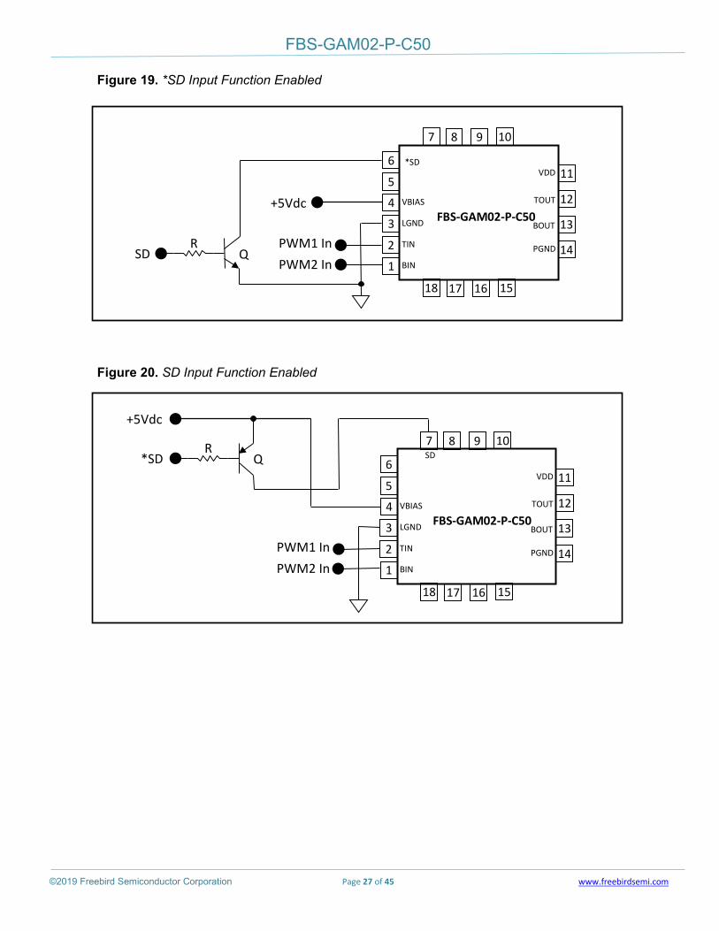
Figure 23. Maximum Switching Frequency Versus Supply Voltage (Vdd) Versus Module Case Temperature (Tc), Io = 10A, Half-Bridge Configuration.
0
10
20
30
40
50
60
200 300 400 500 600 700 800 900 1000
Switching Frequency (kHz)
Vdd
(Vdc
)
110C
85C
70C
Io = 10Adc
FBS-GAM02-P-C50
©2019 Freebird Semiconductor Corporation Page 33 of 45 www.freebirdsemi.com
Figure 24. Maximum Switching Frequency Versus Supply Voltage (Vdd) Versus Module Case Temperature (Tc), Io = 10A, Half-Bridge Configuration.
0
10
20
30
40
50
60
1.0 1.2 1.4 1.6 1.8 2.0
Switching Frequency (MHz)
Vdd
(Vdc
) 110C
85C
70C
50C
35C
Io = 10Adc
FBS-GAM02-P-C50
©2019 Freebird Semiconductor Corporation Page 34 of 45 www.freebirdsemi.com
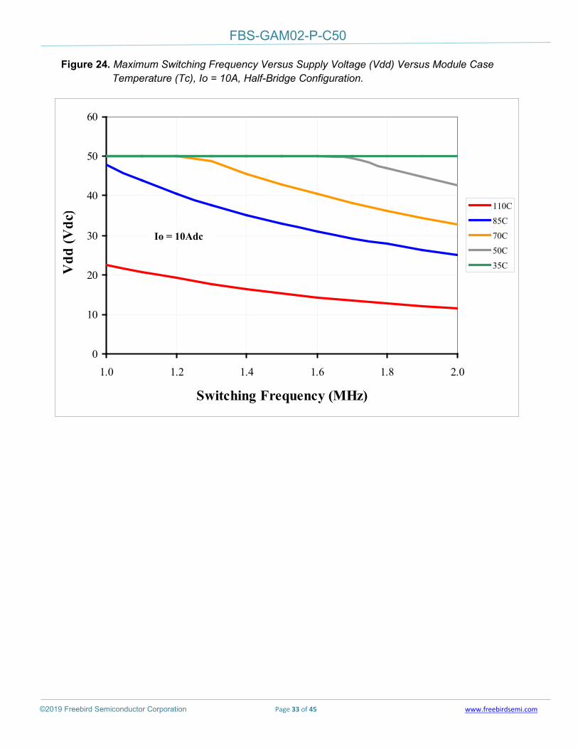
Figure 25. Maximum Output Current (Io) Versus Switching Frequency (fsw) Versus Module Case Temperature (Tc), Vdd = 50V, Half-Bridge Configuration.
0
2
4
6
8
10
12
200 300 400 500 600 700 800 900 1000
Switching Frequency (kHz)
Io (A
dc) 110C
85C
70C
Vdd = 50dc

FBS-GAM02-P-C50
©2019 Freebird Semiconductor Corporation Page 35 of 45 www.freebirdsemi.com
Figure 26. Maximum Output Current (Io) Versus Switching Frequency (fsw) Versus Module Case Temperature (Tc), Vdd = 25V, Half-Bridge Configuration.
0
2
4
6
8
10
12
1.0 1.2 1.4 1.6 1.8 2.0
Switching Frequency (MHz)
Io (A
dc)
110C
85C
Vdd = 25dc
FBS-GAM02-P-C50
©2019 Freebird Semiconductor Corporation Page 36 of 45 www.freebirdsemi.com
Figure 27. Maximum Dead Time (tdt) Versus Switching Frequency (fsw) Versus Module Case Temperature (Tc), Vdd = 25V, Half-Bridge Configuration (Refer to Fig. 23).
FBS-GAM02-P-C50
©2019 Freebird Semiconductor Corporation Page 37 of 45 www.freebirdsemi.com
Figure 28. Maximum Dead Time (tdt) Versus Switching Frequency (fsw) Versus Module Case Temperature (Tc), Io = 10A, Half-Bridge Configuration (Refer to Fig. 21).

FBS-GAM02-P-C50
©2019 Freebird Semiconductor Corporation Page 38 of 45 www.freebirdsemi.com
Radiation Characteristics
The FBS-GAM02-P-C50 (Commerce Rated EAR-99 Device) is an Industrial Level Non-Radiation Hardness Assured Multi-Functional Development Module. The module also provides a forward form-fit function development vehicle for our available, FBS-GAM02-P-R50 Epoxy Over-Molded, Radiation Rated, Commercial Space Series alternatively as an electrically similar development vehicle for future Hermetic Radiation Hardened Ceramic FBS-GAM02-C-R50.
(FBS-M-702-19-001-x Datasheet @ http://www.freebirdsemi.com/universal-gams/ ) FBS-GAM02-P-R50 for form-fit-functional information
Radiation Hardened Assured (RHA) Version Brief Detail:
• Freebird Semiconductor FBS-GAM02-P-R50 (Commerce Rated 9A515.x Device) incorporates internally utilized eGaN® HEMT technology designed, fabricated and tested per Mil-Std-750 Method 1019 for total ionizing dose validation with an in-situ Gamma Bias for (i) VGS = 5.1V, (ii) VDS=VGS=0V and (iii) VDS=80% BVDSS.
• Under the above prescribed conditions Freebird Semiconductor can guarantee full parametric data limits as outlined within the FBS-GAM02-P-R50 datasheet with pre/post radiation effects guarantee under a best practice commercial screened reliability level.
When incorporating Freebird Semiconductors radiation validated HEMT materials the FBS-GAM02-P-R50 series are then “guaranteed by designed” to survive High Dose Rate TID to levels of no less than 100 kRad (Si) with Single Event Immunity to:
Heavy Ion: Au, Silicon ~LET rating= 83.7, 2482 MeV, Range = 130um
FBS-GAM02-P-C50
©2019 Freebird Semiconductor Corporation Page 39 of 45 www.freebirdsemi.com
THERMAL CHARACTERISTICS
Figure 29.Typical Low- or High-Side Power eGAN® HEMT Normalized Junction-to-Case Thermal Impedance
Figure 30. Typical Low- or High-Side Catch Schottky Normalized Junction-to-Case Thermal Impedance
FBS-GAM02-P-C50
©2019 Freebird Semiconductor Corporation Page 40 of 45 www.freebirdsemi.com
PACKAGE OUTLINE AND DIMENSIONS AND PART MARKING
Figure 31. FBS-GAM02-P-C50 Package Outline, Dimensions and Part Marking
YYWW 7FWA3 FBS-GAM02-P-C50
XXXX
Part Marking (See Inset)
Part Marking
Inset
Date Code CAGE Code
Serial Number

FBS-GAM02-P-C50
©2019 Freebird Semiconductor Corporation Page 41 of 45 www.freebirdsemi.com
RECOMMENDED PCB SOLDER PAD CONFIGURATION
The novel I/O “pillar” pads fabricated onto the low-side surface of the FBS-GAM02-P-C50 module are
designed to provide optimal electrical, thermal and mechanical properties for the end-use system designer. To
achieve the full benefit of these properties, it is important that the FBS-GAM02-P-C50 module be soldered to the PCB
motherboard using SN63 (or equivalent) solder. Care should be taken during processing to insure there is minimal
solder voiding in the contacts to the VDD (pin 11), TOUT (pin 12), BOUT (pin 13) and PGND (Pin 14) pads on the
module. The recommended pad dimensions and locations are shown in Figure 32. All dimensions are shown in
inches.
Figure 32. Recommended PCB Solder Pad Configuration (Top View)
FBS-GAM02-P-C50
©2019 Freebird Semiconductor Corporation Page 42 of 45 www.freebirdsemi.com
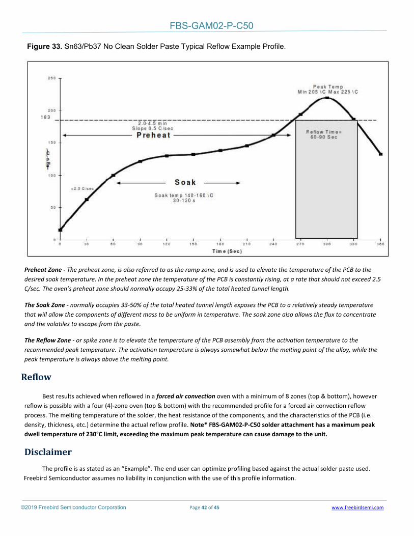
Figure 33. Sn63/Pb37 No Clean Solder Paste Typical Reflow Example Profile.
Preheat Zone - The preheat zone, is also referred to as the ramp zone, and is used to elevate the temperature of the PCB to the desired soak temperature. In the preheat zone the temperature of the PCB is constantly rising, at a rate that should not exceed 2.5 C/sec. The oven’s preheat zone should normally occupy 25-33% of the total heated tunnel length.
The Soak Zone - normally occupies 33-50% of the total heated tunnel length exposes the PCB to a relatively steady temperature that will allow the components of different mass to be uniform in temperature. The soak zone also allows the flux to concentrate and the volatiles to escape from the paste.
The Reflow Zone - or spike zone is to elevate the temperature of the PCB assembly from the activation temperature to the recommended peak temperature. The activation temperature is always somewhat below the melting point of the alloy, while the peak temperature is always above the melting point.
Reflow
Best results achieved when reflowed in a forced air convection oven with a minimum of 8 zones (top & bottom), however reflow is possible with a four (4)-zone oven (top & bottom) with the recommended profile for a forced air convection reflow process. The melting temperature of the solder, the heat resistance of the components, and the characteristics of the PCB (i.e. density, thickness, etc.) determine the actual reflow profile. Note* FBS-GAM02-P-C50 solder attachment has a maximum peak dwell temperature of 230°C limit, exceeding the maximum peak temperature can cause damage to the unit.
Disclaimer The profile is as stated as an “Example”. The end user can optimize profiling based against the actual solder paste used.
Freebird Semiconductor assumes no liability in conjunction with the use of this profile information.
FBS-GAM02-P-C50
©2019 Freebird Semiconductor Corporation Page 43 of 45 www.freebirdsemi.com
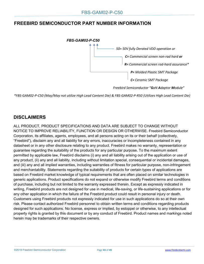
FREEBIRD SEMICONDUCTOR PART NUMBER INFORMATION
FBS-GAM02-P-C50
50= 50V fully Derated VDD operation or
C= Commercial screen non-rad hard or
R= Commercial screen rad-hard assurance*
P= Molded Plastic SMT Package
C= Ceramic SMT Package
Freebird Semiconductor “GaN Adaptor Module”
*FBS-GAM02-P-C50 (May/May not utilize High Lead Content Die) & FBS-GAM02-P-R50 (Utilizes High Lead Content Die)
DISCLAIMERS
ALL PRODUCT, PRODUCT SPECIFICATIONS AND DATA ARE SUBJECT TO CHANGE WITHOUT NOTICE TO IMPROVE RELIABILITY, FUNCTION OR DESIGN OR OTHERWISE. Freebird Semiconductor Corporation, its affiliates, agents, employees, and all persons acting on its or their behalf (collectively, “Freebird”), disclaim any and all liability for any errors, inaccuracies or incompleteness contained in any datasheet or in any other disclosure relating to any product. Freebird makes no warranty, representation or guarantee regarding the suitability of the products for any particular purpose. To the maximum extent permitted by applicable law, Freebird disclaims (i) any and all liability arising out of the application or use of any product, (ii) any and all liability, including without limitation special, consequential or incidental damages, and (iii) any and all implied warranties, including warranties of fitness for particular purpose, non-infringement and merchantability. Statements regarding the suitability of products for certain types of applications are based on Freebird market knowledge of typical requirements that are often placed on similar technologies in generic applications. Product specifications do not expand or otherwise modify Freebird terms and conditions of purchase, including but not limited to the warranty expressed therein. Except as expressly indicated in writing, Freebird products are not designed for use in medical, life-saving, or life-sustaining applications or for any other application in which the failure of the Freebird product could result in personal injury or death. Customers using Freebird products not expressly indicated for use in such applications do so at their own risk. Please contact authorized Freebird personnel to obtain written terms and conditions regarding products designed for such applications. No license, express or implied, by estoppel or otherwise, to any intellectual property rights is granted by this document or by any conduct of Freebird. Product names and markings noted herein may be trademarks of their respective owners.

FBS-GAM02-P-C50
©2019 Freebird Semiconductor Corporation Page 44 of 45 www.freebirdsemi.com
Export Administration Regulations (EAR)
The products described in this datasheet could be subjected to the Export Administration Regulations (EAR). They may require an approved export license prior to export from the United States. An export includes release of product or disclosure of technology to a foreign national inside or outside the United States.
International Traffic in Arms Regulations (ITAR)
The products described in this datasheet could be subjected to the International in Arms Regulations (ITAR). They require an approved export license prior to export from the United States. An export includes release of product or disclosure of technology to a foreign national inside or outside the United States.
Patents
Freebird Semiconductor holds numerous U.S and international patents. US 10,122,274 B2 15/374,756, 15/374,774, PCT/US2016/065952, PCT/US2016/065946. Any that apply to the product(s) listed in this document are identified by markings on the product(s) or on internal components of the product(s) in accordance with U.S Patent laws eGaN© is a registered trademark of Efficient Power Conversion Corporation, Inc.
Data and specification subject to change without notice.

FBS-GAM02-P-C50
©2019 Freebird Semiconductor Corporation Page 45 of 45 www.freebirdsemi.com
REVISION
Datasheet Revision Product Status REV P Proposal/development REV Q Characterization and Qualification -x (x is letter indicating revision) Production Released (FBS-M-702-19-002-x)
Change History:
1. Modified document number on data sheets has been changed from FBS-S Identifier to FBS-M AS9100D implementation (Rev B) 2. Modified all operational & case temperature limits from 110oC down to 85oC for developmental unit (Rev B) 3. Modified dead time detail Bout to Tout/ Tout to Bout external requirement information (Rev B) 4. Modified VBias minimum voltage to 4.75V from original 4.5V (For FBS-GAM02-P-C50 ONLY) (Rev B) 5. OVLO language revised to indicate “OVLO activation is indicative of potential catastrophic voltage applied to unit” (Rev B) 6. Reformatted Dynamic Electrical Data for Better User Clarity along with added high temperature detail (Rev C) 7. Added New INTERFACING THE FBS-GAM02 TO LEGACY RAD-HARD PWM CONTROLLERS Application Section (Rev C) 8. Added New Adaptive Dead Time Control Applications Section For the FBS-GAM02-P-C50 (Rev C)
Contact Freebird Semiconductor Corporation for further information and to order: Email : [email protected]
Phone: +1 941 740 1909 Website: www.Freebirdsemi.com Address: 17 Parkridge Road, Unit E
Haverhill, MA 01835
Freebird Semiconductor Corporation has been assessed and registered by Intertek as conforming to the requirements of AS9100D and ISO 9001:2015 quality management system which is applicable to the design and manufacture of high reliability semiconductors devices and circuits. The assessment was performed in accordance with the requirements of AS9104/1:2012-01. Intertek is accredited under the Aerospace Management Program and IAQG ICOP scheme.